EP3138050B1 - Aus mott-isolatoren hergestelltes, einkomponentiges künstliches neuron, netz aus künstlichen neuronen und verfahren zur herstellung der besagten künstlichen neuronen - Google Patents
Aus mott-isolatoren hergestelltes, einkomponentiges künstliches neuron, netz aus künstlichen neuronen und verfahren zur herstellung der besagten künstlichen neuronen Download PDFInfo
- Publication number
- EP3138050B1 EP3138050B1 EP15718863.2A EP15718863A EP3138050B1 EP 3138050 B1 EP3138050 B1 EP 3138050B1 EP 15718863 A EP15718863 A EP 15718863A EP 3138050 B1 EP3138050 B1 EP 3138050B1
- Authority
- EP
- European Patent Office
- Prior art keywords
- artificial neuron
- artificial
- mott
- neuron
- layer
- Prior art date
- Legal status (The legal status is an assumption and is not a legal conclusion. Google has not performed a legal analysis and makes no representation as to the accuracy of the status listed.)
- Active
Links
Images


Classifications
-
- G—PHYSICS
- G06—COMPUTING OR CALCULATING; COUNTING
- G06N—COMPUTING ARRANGEMENTS BASED ON SPECIFIC COMPUTATIONAL MODELS
- G06N3/00—Computing arrangements based on biological models
- G06N3/02—Neural networks
- G06N3/06—Physical realisation, i.e. hardware implementation of neural networks, neurons or parts of neurons
- G06N3/063—Physical realisation, i.e. hardware implementation of neural networks, neurons or parts of neurons using electronic means
-
- G—PHYSICS
- G06—COMPUTING OR CALCULATING; COUNTING
- G06N—COMPUTING ARRANGEMENTS BASED ON SPECIFIC COMPUTATIONAL MODELS
- G06N3/00—Computing arrangements based on biological models
- G06N3/02—Neural networks
- G06N3/04—Architecture, e.g. interconnection topology
- G06N3/049—Temporal neural networks, e.g. delay elements, oscillating neurons or pulsed inputs
-
- G—PHYSICS
- G06—COMPUTING OR CALCULATING; COUNTING
- G06N—COMPUTING ARRANGEMENTS BASED ON SPECIFIC COMPUTATIONAL MODELS
- G06N3/00—Computing arrangements based on biological models
- G06N3/02—Neural networks
- G06N3/06—Physical realisation, i.e. hardware implementation of neural networks, neurons or parts of neurons
- G06N3/063—Physical realisation, i.e. hardware implementation of neural networks, neurons or parts of neurons using electronic means
- G06N3/065—Analogue means
-
- G—PHYSICS
- G11—INFORMATION STORAGE
- G11C—STATIC STORES
- G11C11/00—Digital stores characterised by the use of particular electric or magnetic storage elements; Storage elements therefor
- G11C11/54—Digital stores characterised by the use of particular electric or magnetic storage elements; Storage elements therefor using elements simulating biological cells, e.g. neuron
-
- G—PHYSICS
- G11—INFORMATION STORAGE
- G11C—STATIC STORES
- G11C13/00—Digital stores characterised by the use of storage elements not covered by groups G11C11/00, G11C23/00, or G11C25/00
- G11C13/0002—Digital stores characterised by the use of storage elements not covered by groups G11C11/00, G11C23/00, or G11C25/00 using resistive RAM [RRAM] elements
-
- H—ELECTRICITY
- H10—SEMICONDUCTOR DEVICES; ELECTRIC SOLID-STATE DEVICES NOT OTHERWISE PROVIDED FOR
- H10N—ELECTRIC SOLID-STATE DEVICES NOT OTHERWISE PROVIDED FOR
- H10N70/00—Solid-state devices having no potential barriers, and specially adapted for rectifying, amplifying, oscillating or switching
- H10N70/011—Manufacture or treatment of multistable switching devices
-
- H—ELECTRICITY
- H10—SEMICONDUCTOR DEVICES; ELECTRIC SOLID-STATE DEVICES NOT OTHERWISE PROVIDED FOR
- H10N—ELECTRIC SOLID-STATE DEVICES NOT OTHERWISE PROVIDED FOR
- H10N70/00—Solid-state devices having no potential barriers, and specially adapted for rectifying, amplifying, oscillating or switching
- H10N70/801—Constructional details of multistable switching devices
- H10N70/841—Electrodes
-
- H—ELECTRICITY
- H10—SEMICONDUCTOR DEVICES; ELECTRIC SOLID-STATE DEVICES NOT OTHERWISE PROVIDED FOR
- H10N—ELECTRIC SOLID-STATE DEVICES NOT OTHERWISE PROVIDED FOR
- H10N70/00—Solid-state devices having no potential barriers, and specially adapted for rectifying, amplifying, oscillating or switching
- H10N70/801—Constructional details of multistable switching devices
- H10N70/881—Switching materials
Definitions
- the field of the invention is that of neuromorphic electronic circuits, and more particularly that of artificial neurons.
- the invention relates to a new design of an artificial neuron.
- the invention has applications notably, but not exclusively, in the field of artificial intelligence, and more particularly, in the field of associative memories, of image and sound recognition methods, or even in the field of methods.
- learning or self-learning implemented by artificial neural networks allow the extraction of knowledge organized from real or simulated data according to the following principle: data considered to be similar are grouped together in the same group while data considered to be different are divided into groups distinct.
- a promising path therefore consists in developing an electronic architecture of the neuromorphic type, made up of artificial neurons and synapses imitating the architecture of the human brain.
- the human brain is made up of a network of 10 11 neurons linked together by 10 15 synapses.
- the data is stored in the memory of the human brain thanks to the different levels of conductance of the synapses, commonly known as synaptic weights. Therefore, the realization of an artificial brain goes through the realization of artificial neural networks that mimic the interconnection of neurons via synapses.
- Artificial neural networks are essentially composed of neurons interconnected with each other by synapses.
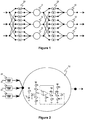
- the figure 1 for example presents a neuromorphic architecture, called a multilayer perceptron, composed of six neurons (referenced 10) and eighteen synapses (referenced 20).
- Synaptic weight is represented by the letter w.
- these neural networks are "virtual”, that is to say implemented by computer programs (called “Software Neural Networks” in English) using computers with conventional architecture, which decreases their efficiency. , especially in terms of energy consumption.
- FIG. 2 An exemplary embodiment of a multi-component artificial neuron 10 according to the state of the art is illustrated in figure 2 .
- This neuron 10 requires the implantation, on a printed circuit, of a large number of electronic components such as transistors (for example in CMOS technology), amplifiers and capacitors, components arranged according to a relatively complex architecture.
- the implantation of different components is a relatively complex operation, many components having to be placed on an increasingly small surface, due to the requirements of miniaturization.
- the assembly still occupies a certain area, which is difficult to reduce.
- such complexity is highly detrimental to the overall performance of the electronic circuit, in terms of integration and energy efficiency.
- an artificial neuron must perform several functions.
- an artificial impulse neuron ( “spiking neuron” ) must react to the application of trains of electrical impulses. Indeed, it is in this form of impulses ( “spikes”) that information circulates in the most promising artificial neural networks.
- an artificial neuron should ideally reproduce a behavior similar to that described by the standard model LIF (for “Leaky, Integrate and Fire”), that is to say a behavior implementing the following three functions: integration, flight and shooting.
- LIF for “Leaky, Integrate and Fire”
- the LIF model postulates that there is a single threshold for v ( t ), independent of the shape of the input signal, beyond which the artificial neuron LIF triggers the “shot” function.
- the input electrical signal S (t) is a sequence of square electrical pulses of the same amplitude
- N Fire represents the number of electrical pulses necessary to trigger the “fire” function
- t is the duration of application of each electrical pulse
- t off the time elapsing between two successive electrical pulses (see figure 9 )
- MD PICKETT ET AL "A scalable neuristor built with Mott memristors", NATURE MATERIALS, vol. 12, no. 2, December 16, 2012 (2012-12-16), pages 114-117 relates to an electronic circuit designated under the term of “neurositor” whose behavior is similar to that of a neuron of the “Hodgkin-Huxley” type.
- This neuristor circuit includes memristive components as well as other classical elementary electronic components.
- the object of the invention in at least one embodiment, is in particular to overcome these various drawbacks of the state of the art.
- an objective is to provide an artificial neuron of a new design, which is simple to produce.
- the objective of at least one embodiment of the invention is also to provide an artificial neuron which offers a high potential for integration into electronic circuits.
- the invention provides an artificial neuron according to independent claim 1.
- the term “electric dipole” is understood to mean an electronic component having two terminals.
- the single-component artificial neuron consists of a single electrical dipole, itself made of an insulating material of Mott between two electric electrodes.
- this dipole is subjected to a succession of electrical pulses (representative of information coming from the synapses), it performs the three elementary functions of an artificial neuron as described in the reference model LIF, namely the integration with flight and shooting.
- the one-component artificial neuron according to the invention requires little energy and has a high potential for integration into electronic circuits.
- the artificial neuron comprises an input and an output.
- the artificial neuron is such that a first end of the electric dipole comprises a first electric electrode which constitutes said input and that a second end of the electric dipole comprises a second electric electrode which constitutes said output of the artificial neuron.
- the structure of the artificial neuron can be broken down according to several particular embodiments.
- the structure of the artificial neuron can be assimilated to a three-dimensional structure.
- the structure of the artificial neuron can be likened to a two-dimensional structure.
- the structure of the artificial neuron can be assimilated to a one-dimensional structure.
- each artificial neuron of the network is a single-component artificial neuron according to the invention.
- the single-component artificial neuron obtained according to the invention is therefore very simple to manufacture. It should be noted that the step of depositing the electrical electrodes can be carried out either before or after the Mott insulator has been deposited.
- said step of obtaining a material comprises a step of cutting a block of crystal belonging to the family of Mott insulators and said step of depositing a layer of conductive material is carried out as a function of said cut crystal block.
- said step of obtaining a material comprises a step of depositing, on a substrate plate, a thin layer based on a material belonging to the Mott family of insulators, said step of deposition of a layer of conductive material at the first and second ends being performed as a function of said deposited thin layer.
- said step of obtaining a material comprises a step of depositing, on a substrate plate, a nanotube or a nanowire based on a material belonging to the family of insulators of Mott, said step of depositing a layer of conductive material at the first and second ends being performed as a function of said deposited nanotube or nanowire.
- the invention proposes a one-component artificial neuron of a novel design conforming to the reference model LIF ( “Leaky Integrate and Fire” ).
- the figure 3 presents an example of the structure of a one-component artificial neuron 30 according to a first particular embodiment of the invention (three-dimensional structure).
- the single-component artificial neuron 30 represented in this figure consists of a single electric dipole comprising a piece of crystal material 31 belonging to the family of Mott insulators, for example the compound of formula GaTa 4 Se 8 , connected by two electrodes 32 and 33.
- the two electrodes 32, 33 are each made of an electrically conductive material.
- the one-component artificial neuron 30 thus obtained according to the invention is of the integrated type with leakage and pulling, that is to say it fulfills the three functions of the artificial neuron in accordance with the reference model LIF.
- the insulating material of Mott 31 is a cut crystal block 20 ⁇ m thick, 300 ⁇ m long and 200 ⁇ m wide.
- Each electrical electrode is typically in the form of a thin layer 0.1 ⁇ m thick, 300 ⁇ m long and 200 ⁇ m wide. It should be noted that these dimensions are given purely for illustration and may of course be different.
- the neuron 30 according to the invention is assimilated to a three-dimensional (3D) artificial neuron.
- the dimensions of the Mott insulating crystal piece 31, the electric electrodes 32, 33 and their arrangement with respect to said crystal piece, as well as the choice of materials can be optimized so that the mono artificial neuron component 30 thus obtained can benefit from the best performance (quality of the response of the electric dipole compared to that expected in the LIF model of the artificial neuron, structural integration, etc.).
- the first step is to cut a piece of GaTa 4 Se 8 crystal constituting the functional material of the mono-component artificial neuron 30. Then, on the two opposite faces of the piece of crystal 31, the deposit is made. a conductive material constituting the input electrodes 32 (denoted “INPUT” in the figure) and output 33 (denoted "OUTPUT” in the figure) of the artificial neuron.
- This deposition can typically be carried out either by applying a conductive lacquer directly to the faces of the crystal or by using a deposition technique such as for example evaporation by the Joule effect or magnetron sputtering (PVD for “Physical Vapor Deposition”).
- PVD Magnetron sputtering
- the figures 4A and 4B present two examples of the structure of a one-component artificial neuron 30 according to a second particular embodiment of the invention (two-dimensional structure).
- the one-component artificial neuron 40A shown in figure 4A consists of a single electric dipole comprising a layer of material 41A belonging to the family of Mott insulators, for example the compound of formula GaV 4 S 8 , connected by two electrically conductive electrodes 42A and 43A.
- the electric dipole is supported by an insulating substrate 44A. It is therefore the electric dipole 40A as a simple elementary electronic component which behaves like an artificial neuron, the insulating substrate 44A only playing the role of support for the device of the invention.
- the one-component artificial neuron 40A thus obtained according to the invention is of the integrated type with leakage and pulling, that is to say it fulfills the three functions of the artificial neuron in accordance with the reference model LIF.
- the first electrode 42A is in the form of an L is disposed in part on a first end of the Mott insulation layer 41A, the other part extending over the substrate. insulator 44A.
- This electrode forms the input of the one-component artificial neuron 40A (denoted “INPUT” in the figure).
- the second electrode 43A is in the shape of an L and is disposed partly on the second end of the Mott insulating layer 41A, the other part extending over the insulating substrate 44A. This electrode forms the output of the one-component artificial neuron 40A (denoted “OUTPUT” in the figure).
- the set of electrodes 42A, 43A is placed on the Mott insulating layer 41A, in other words once the Mott insulating layer 41A has been deposited on the substrate 44A.
- This is of course an example of a particular structure. It is clear that many other single-component artificial neuron structures can be envisaged, without departing from the scope of the invention. For example, provision can be made for a neuron structure according to which the electrodes are arranged under the Mott insulation layer 41A (as is the case in the particular embodiment illustrated in figure 6 ). Provision can also be made, for example, for the Mott insulation layer to be sandwiched between the electrodes, as shown in FIG. figure 4B . Likewise, the shape and dimensions of the electrodes can also vary depending on the desired neuromorphic architecture.
- the one-component artificial neuron 40B shown in the figure 4B consists of a single electric dipole comprising a layer of material 41B, of formula GaV 4 S 8 , sandwiched between the electrodes 42A and 43A. The whole is arranged on a substrate plate 44B.
- the layer of Mott insulating material is a thin layer 0.1 ⁇ m thick, 20 ⁇ m long and 1 ⁇ m wide.
- Each electrode has a thickness of 0.1 ⁇ m.
- thin layer is understood to mean a layer of material whose thickness is generally less than 10 ⁇ m, as opposed to “thick layers” whose thickness is generally greater than 10 ⁇ m.
- the thin layer of Mott insulating material has a two-dimensional (2D) structure.
- the neuron 40A or 40B according to the invention can therefore be likened to a two-dimensional (2D) artificial neuron.
- the dimensions of the Mott insulation layer, the metal electrodes and their arrangement with respect to said layer, as well as the choice of materials can be optimized so that the one-component artificial neuron thus obtained can benefit from the best performances (quality of the response of the electric dipole compared to that expected in the LIF model of the artificial neuron, structural integration, etc.).
- a layer of GaV 4 S 8 constituting the functional material of the one-component artificial neuron 40A is deposited on a substrate wafer (an oxidized silicon wafer for example).
- This deposition can typically be carried out by means of a deposition technique such as for example: evaporation by the Joule effect, magnetron sputtering (PVD), deposition by laser pulses (PLD for “Pulse Laser Deposition” ), deposition by atomic layer (ALD for "Atomic Layer Deposition” ), deposition by chemical solutions (CSD for "Chemical solution deposition” ), deposition by screen printing, deposition by spinning / dipping (" Spin / Dip coating” in English).
- PVD magnetron sputtering
- PLAD magnetron sputtering
- ALD Atomic Layer Deposition
- CSD chemical solution deposition
- the first step is to deposit, on a substrate wafer (an oxidized silicon wafer for example), a layer of metallic material constituting the output electrode 43B according to a technique evaporation by Joule effect or magnetron sputtering for example. Then, one proceeds to the deposition on said layer of metallic material 43B of a layer of GaV 4 S 8 constituting the functional material 41B of the one-component artificial neuron 40B by means of one of the deposition techniques described above in relation to the figure 4A . Finally, another layer of metallic material constituting the input electrode 42B of the neuron is deposited.
- the figures 5A and 5B present two examples of the structure of a single-component artificial neuron according to a third particular embodiment of the invention (one-dimensional structure).
- the one-component artificial neuron 50A shown in figure 5A consists of a single electrical dipole comprising a nanowire of Mott insulator 51A of formula (V 1-x Cr x ) 2 O 3 , connected by two electrodes 52A and 53A.
- the electric dipole is supported by an insulating substrate 54A. It is therefore the electric dipole 50A as a simple elementary electronic component which behaves like an artificial neuron, the insulating substrate 54A only playing the role of support for the device of the invention.
- the one-component artificial neuron 50A thus obtained according to the invention is of the integrates type with leakage and pull, that is to say it fulfills the three functions of the artificial neuron in accordance with the reference model LIF.
- the first electrode 52A is disposed in part under a first end of the Mott insulating nanowire 51A, the other part extending over the insulating substrate 54A.
- This electrode forms the input of the one-component artificial neuron 50A (denoted “INPUT” in the figure).
- the second electrode 53A is disposed in part under the second end of the Mott insulation nanowire 51A, the other part extending over the insulating substrate 54A.
- This electrode forms the output of the one-component artificial neuron 50A (denoted “OUTPUT” in the figure).
- the set of electrodes 52A, 53A is placed under the Mott insulating nanowire 51A, in other words before the Mott insulating nanowire 51A has been deposited on the substrate 54A.
- This is of course an example of a particular structure. It is clear that many other single-component artificial neuron structures can be envisaged, without departing from the scope of the invention.
- the first step is to deposit, on a substrate wafer (a silicon wafer for example), a layer of metallic material constituting the two input and output electrodes of the neuron.
- This deposition can typically be carried out by means of one of the following techniques, for example: Joule effect evaporation, magnetron sputtering (PVD), laser pulse deposition (PLD), atomic layer deposition (ALD), deposition by chemical solutions ( CSD), deposition by screen printing, deposition by spinning / dipping ( "Spin / Dip coating” ).
- PVD magnetron sputtering
- PLD laser pulse deposition
- ALD atomic layer deposition
- CSD deposition by chemical solutions
- deposition by screen printing deposition by spinning / dipping ( "Spin / Dip coating” ).
- VLS Vapor-Liquid-Solid
- figure 5B differs from that of the figure 5A in that the artificial neuron 50B consists, not of a nanowire of Mott insulation, but of a nanotube of Mott insulation 51B.
- the rest of the structure of this artificial neuron 50B is identical to the artificial neuron 50A.
- An input conductive electrode 52B is arranged under the nanotube 51B at one of its ends and an output conductive electrode 53B is arranged under the nanotube 51B at the other of its ends, the everything being disposed on an insulating substrate 54B.
- the artificial neuron 50C shown in the figure 5C consists of an electric dipole comprising a nanowire of Mott insulator 51C of formula V 2-x Cr x O 3 , connected by two electrodes 52C and 53C.
- the electric dipole is supported by an insulating substrate 54C of general L-shape, having two substantially parallel surfaces 56 and 57 on which are respectively arranged the layers of material forming the input 52C and output 53C electrodes of the device. artificial neuron.
- the two surfaces 56 and 57 are connected by a third surface 58 on which the nanowire 51C is arranged so that the end sections thereof are connected to the input 52C and output 53C electrodes of the neuron.
- the first step is to deposit, on the L-shaped substrate, at the level of the surface 57, a layer of metallic material constituting the output electrode 53C of the neuron, for example by evaporation by the Joule effect.
- the nanowire 51C is arranged so that one of its ends is in contact with the output electrode 53C and so that part of the circumferential surface of the nanowire extends along the surface 58 towards the surface 56, the nanowire having been previously synthesized by means of a Vapor-Liquid-Solid (VLS) or template method for example.
- VLS Vapor-Liquid-Solid
- another layer of metallic material is deposited at the level of the free end of the nanowire and of the surface 56 to constitute the input electrode 52C of the neuron, for example by evaporation by the Joule effect.
- the Mott insulation nanowire or nanotube is considered to have a one-dimensional (1D) structure.
- the neuron 50A, 50B or 50C according to the invention can therefore be likened to a one-dimensional artificial neuron (1D).
- the input and output electrodes can be made from one of the following materials: a single element such as Platinum (Pt), Gold (Au), Silver (Ag), Molybdenum (Mo), Graphite (C), Aluminum (Al), Copper (Cu), doped silicon (Si)) or an alloy such as brass, steel, bronze for example or a compound of transition metals such as TiN, TaN, RuO 2 , SrRuO 3 , CuS 2 .
- a single element such as Platinum (Pt), Gold (Au), Silver (Ag), Molybdenum (Mo), Graphite (C), Aluminum (Al), Copper (Cu), doped silicon (Si)
- an alloy such as brass, steel, bronze for example or a compound of transition metals such as TiN, TaN, RuO 2 , SrRuO 3 , CuS 2 .
- each electrode of the one-component artificial neuron as described above is configured to be connected to one or more artificial synapses (not shown in the figure), such as for example the artificial synapses w according to the neuromorphic architecture shown in the figure figure 1 (where each artificial neuron is configured to be connected to a set of three input synapses and three output synapses).
- one or more artificial synapses such as for example the artificial synapses w according to the neuromorphic architecture shown in the figure figure 1 (where each artificial neuron is configured to be connected to a set of three input synapses and three output synapses).
- the neural network according to the invention comprises a plurality of artificial neurons interconnected with one another by artificial synapses.
- a network of artificial neurons some of which are mono-component artificial neurons according to the invention and others are neurons of the state of the art.
- each artificial neuron of the network is a single-component artificial neuron as defined according to the invention.
- the figure 6 presents a network of three mono-component artificial neurons 60 1 , 60 2 , 60 3 , according to a particular embodiment of the invention.
- the single-component artificial neuron 60 1 is formed of an electric dipole comprising a thin layer 61 1 of GaV 4 S 8 material , the ends of which are brought into contact with a set of metal electrodes playing the role of input / output of the neuron: the first end of said GaV 4 S 8 layer is contacted with input electrode 62 1 and the second end of said GaV 4 S 8 layer is contacted with output electrode 63 1 .
- the single-component artificial neuron 60 2 is formed of an electric dipole comprising a thin layer 61 2 of GaV 4 S 8 material , the ends of which are brought into contact with a set of metal electrodes playing the role of input / output of the neuron: the first end of said GaV 4 S 8 layer is contacted with input electrode 62 2 and the second end of said GaV 4 S 8 layer is contacted with output electrode 63 2 .
- the single-component artificial neuron 60 3 is formed of an electric dipole comprising a thin layer 61 3 of GaV 4 S 8 material , the ends of which are brought into contact with a set of metal electrodes playing the role of input / output of the neuron: the first end of said GaV 4 S 8 layer is contacted with input electrode 62 3 and the second end of said GaV 4 S 8 layer is contacted with output electrode 63 3 .
- Each one-component artificial neuron was obtained by means of the manufacturing process described above in relation to the figure 3 on a plate of insulating substrate 64 with the difference that the input / output electrodes are here of straight elongated shape and that they are placed below the thin layers of GaV 4 S 8 .
- these one-component artificial neurons can be connected to artificial synapses (not shown in the figure) at the input (INPUT) and the output (OUTPUT) of each neuron so as to integrate a neural network.
- artificial such as the example of neuromorphic architecture shown in the figure 1 where each neuron is connected to a set of three input synapses and three output synapses).
- artificial neural networks with, on the one hand, a number of artificial neurons greater than three and, on the other hand, comprising artificial neurons either based on a piece of Mott's insulating crystal, or based on Thin layer of Mott insulation, either nanowire or nanotube based Mott insulation.
- the figures 7A, 7B, 7C present, in the form of chronograms, the evolution of electrical signals illustrating the operating principle of an artificial neuron of the integrated type with leak and pull (LIF).
- An artificial neuron of type LIF receives a series of impulses S (t) weighted by the synaptic weight w ( Figure 7A ).
- the artificial neuron then integrates ( “Integrate” ) a function of this input signal over time; the quantity corresponding to the result of this integration by the artificial neuron relaxes over time ( "Leaky” ) thus giving the signal v ( t ) ( Figure 7B ).
- This signal v ( t ) is the equivalent of the presynaptic membrane potential for a biological neuron.
- the artificial neuron triggers an output signal ( “Fire” ) when the signal v ( t ) reaches a given threshold.
- This output signal S out (t) ( Figure 7C ) is an impulse whose shape is not explicitly defined in the LIF model.
- the artificial neuron according to the LIF model therefore fulfills the following three functions: integration with leakage and firing.
- the experimental part described below shows that the Mott isolators exhibit the properties required to behave like an artificial neuron according to the LIF model.
- the figure 8 represents an experimental set-up used for the application of electrical pulses and the demonstration of the integrated behavior with leakage and pull (LIF) of the single-component artificial neuron in accordance with the invention.
- LIF leakage and pull
- It comprises an electrical pulse generator 83 mounted in series with an experimental device consisting of a conductance denoted " w " 84 playing the role of a artificial synapse itself mounted in series with a piece of crystal of functional material 80 arranged between two metal electrodes 81 and 82.
- the objective was to test the response of the functional material 80 to the application of different series of electrical pulses emitted by the generator 83.
- the functional material 80 is here a piece of GaTa 4 Se 8 crystal which has been synthesized beforehand. , then cleaved. It is about one of the compounds belonging to the family of insulators of Mott AM 4 Q 8 , with A which comprises at least one of the following elements: Ga, Ge, Zn, M which comprises at least one of the following elements: V, Nb, Ta, Mo and Q which comprises at least one of the following elements: S, Se, Te.
- the functional material 80 typically has the following dimensions: 300 ⁇ m long, 200 ⁇ m wide and 20 ⁇ m thick.
- the two metal electrodes 81 and 82 are formed, for example, by means of a carbon lacquer.
- the voltage across conductance “ w ” 84 (denoted V w ) and the voltage across functional material 80 (denoted V) are measured using an oscilloscope.
- the functional material 80 receives electrical signals only from the single pulse generator 83.
- this functional material is connected to several different pulse sources, in order to mimic the large number of synaptic connections that can exist in an artificial neural network.
- the figure 9 schematically illustrates the main characteristics of the series of electrical pulses sent by the generator: the duration t ON of the electrical pulses, the duration t OFF elapsing between two successive pulses, the total voltage V of each pulse and the number N of pulses emitted in the series.
- the figure 10 shows the response of the functional material 80 when the circuit of the figure 8 is subjected to a single electrical pulse of long duration (greater than 100 ⁇ s) and of an amplitude of approximately 60 V.
- This response is here characterized by the voltage V obtained at the terminals of the functional material 80, the current I passing through it and its electrical resistance R.
- the threshold value of the electric field varies in power law with the band gap energy of the Mott insulating compounds and can therefore be determined according to this law. It is therefore possible by the choice of the Mott insulator used to optimize the value of this threshold field according to the desired characteristics.
- the figure 11 presents two experimental curves obtained for the functional material of the experimental set-up of the figure 8 , making it possible to illustrate that the resistance of the functional material returns to its initial state after the pulse and therefore that the resistive transition is volatile.
- the first graph shows the evolution of the total voltage V applied to the functional material 80 and the second graph shows the evolution of its resistance over time.
- the integration phenomenon is also confirmed by a series of experiments carried out by keeping the duration t OFF between two successive pulses constant and by varying the duration t ON of the electrical pulses.
- the figure 12B shows the response of the functional material 80 (output signal l ), when the circuit of the figure 8 is subjected to a series of four electrical pulses with a duration t ON of 20 ⁇ s, separated from each other with a duration t OFF of 30 ⁇ s, and an amplitude of approximately 60 V ( total input signal V ) . So the figure 12B presents the same experiment as that described on the figure 12A , but with an increased duration t ON of the electrical pulses applied to the functional material (we go from a duration t ON from 15 to 20 ⁇ s).
- the figure 12C presents the same experiment as that described on the figure 12A , but with a longer duration t OFF between two successive pulses (170 ⁇ s against 30 ⁇ s previously).
- the result is very clear: the number of electrical pulses necessary for the functional material 80 to trigger an output signal (" spike” ) increased from six to eight pulses.
- spike the number of electrical pulses necessary for the functional material 80 to trigger an output signal
- This proves that the signal integrated by the functional material relaxes over time, which results in a form of leaky .
- the functional material is capable of implementing, not only the functions of integration ( “Integrate” ) and of firing ( “Fire ”), but also the function of leak (“Leaky”) of the standard model. LIF.
- the figure 13 presents the experimental dependence of the number of pulses necessary to fire ( N Fire ) with the duration t on ( figure 13A ) and the duration t off ( figure 13B ) obtained during experiments similar to those described on the figures 12A-C .
Landscapes
- Engineering & Computer Science (AREA)
- Physics & Mathematics (AREA)
- Theoretical Computer Science (AREA)
- Health & Medical Sciences (AREA)
- Life Sciences & Earth Sciences (AREA)
- Biomedical Technology (AREA)
- Biophysics (AREA)
- Molecular Biology (AREA)
- General Health & Medical Sciences (AREA)
- Mathematical Physics (AREA)
- Computational Linguistics (AREA)
- Data Mining & Analysis (AREA)
- Artificial Intelligence (AREA)
- Computing Systems (AREA)
- General Engineering & Computer Science (AREA)
- Evolutionary Computation (AREA)
- Software Systems (AREA)
- General Physics & Mathematics (AREA)
- Neurology (AREA)
- Computer Hardware Design (AREA)
- Manufacturing & Machinery (AREA)
- Semiconductor Memories (AREA)
- Peptides Or Proteins (AREA)
- Non-Volatile Memory (AREA)
Claims (11)
- Künstliches Neuron (30), das die Funktionen Integration, Leck und Feuern umsetzt, dadurch gekennzeichnet, dass das künstliche Neuron ein künstliches Neuron des Referenzmodells "Leaky, Integrate and Fire" ist, und dass es aus einem einzigen elektrischen Einkomponenten-Dipol gebildet ist, aufweisend ein Material (31), das zur Familie der Mott-Isolatoren gehört, verbunden mit zwei elektrischen Elektroden (32, 33).
- Künstliches Neuron gemäß Anspruch 1, wobei das Mott-Isolatormaterial aufweist:- eine Verbindung der Formel AM4Q8, mit A, das mindestens eines der folgenden Elemente aufweist: Ga, Ge, Zn; M, das mindestens eines der folgenden Elemente aufweist: V, Nb, Ta, Mo; und Q, das mindestens eines der folgenden Elemente aufweist: S, Se, Te; oder- eine anorganische Verbindung der Formel (V1-xMx)2O3, wobei 0 ≤ x ≤ 1, wobei M mindestens eines der folgenden Elemente aufweist: Ti, Cr, Fe, Al oder Ga; oder- eine anorganische Verbindung der Formel NiS2-xSex, wobei 0 ≤ x ≤ 1; oder- eine Verbindung der Formel VO2; oder- eine organische Mott-Isolatorverbindung.
- Künstliches Neuron gemäß irgendeinem der Ansprüche 1 und 2, wobei die zwei elektrischen Elektroden (32, 33) jeweils aus einem elektrisch leitfähigen Material gebildet sind, aufweisend:- eines der folgenden Elemente: Platin (Pt), Gold (Au), Molybdän (Mo), Graphit (C), Aluminium (Al), Kupfer (Cu), dotiertes Silicium (Si); oder- eine der folgenden Legierungen: Messing (Cu-Zn), Stahl (Fe-C), Bronze (Cu-Sn); oder- eine der folgenden Übergangsmetallverbindungen: TiN, TaN, RuO2, SrRuO3, CuS2).
- Künstliches Neuron gemäß irgendeinem der Ansprüche 1 bis 3, wobei das Mott-Isolatormaterial:- in Form einer Dünnschicht oder- in Form eines Kristallblocks oder- in Form einer Nanoröhre oder- in Form eines Nanodrahtesvorliegt.
- Neuronales Netzwerk, aufweisend eine Mehrzahl von künstlichen Neuronen, dadurch gekennzeichnet, dass mindestens ein künstliches Neuron gemäß irgendeinem der Ansprüche 1 bis 4 ist.
- Neuromorphe elektronische Schaltung, aufweisend eine Mehrzahl von künstlichen Neuronen, dadurch gekennzeichnet, dass mindestens ein künstliches Neuron gemäß irgendeinem der Ansprüche 1 bis 4 ist.
- Verfahren zum Herstellen eines künstlichen Neurons, das die Funktionen Integration, Leck und Feuern umsetzt, dadurch gekennzeichnet, dass es die folgenden Schritte aufweist:- Erhalten eines Materials, das zur Familie der Mott-Isolatoren gehört,- Erhalten eines künstlichen Neurons des Referenzmodells "Leaky, Integrate and Fire", gebildet aus einem einzigen elektrischen Einkomponenten-Dipol, durch Aufbringen einer Schicht eines leitfähigen Materials:* an einem ersten Ende des Mott-Isolatormaterials, um eine erste elektrische Elektrode zu bilden,* an einem zweiten Ende des Mott-Isolatormaterials, um eine zweite elektrische Elektrode zu bilden.
- Verfahren zum Herstellen gemäß Anspruch 7, wobei der Schritt des Erhaltens eines Materials durch Schneiden eines Mott-Isolator-Kristallblocks durchgeführt wird, und wobei der Schritt des Aufbringens einer Schicht eines leitfähigen Materials in Abhängigkeit von dem geschnittenen Kristallblock durchgeführt wird.
- Verfahren zum Herstellen gemäß Anspruch 7, wobei der Schritt des Erhaltens eines Materials durch Aufbringen einer Dünnschicht eines Mott-Isolatormaterials auf eine Substratplatte durchgeführt wird,
und wobei der Schritt des Aufbringens einer Schicht eines leitfähigen Materials in Abhängigkeit von der aufgebrachten Dünnschicht durchgeführt wird. - Verfahren zum Herstellen gemäß Anspruch 7, wobei der Schritt des Erhaltens eines Materials durch Aufbringen einer Nanoröhre auf Basis eines Mott-Isolatormaterials auf eine Substratplatte durchgeführt wird, und wobei der Schritt des Aufbringens einer Schicht eines leitfähigen Materials in Abhängigkeit von der aufgebrachten Nanoröhre durchgeführt wird.
- Verfahren zum Herstellen gemäß Anspruch 7, wobei der Schritt des Erhaltens eines Materials durch Aufbringen eines Nanodrahtes auf Basis eines Mott-Isolatormaterials auf eine Substratplatte durchgeführt wird,
und wobei der Schritt des Aufbringens einer Schicht eines leitfähigen Materials in Abhängigkeit von dem aufgebrachten Nanodraht durchgeführt wird.
Applications Claiming Priority (2)
| Application Number | Priority Date | Filing Date | Title |
|---|---|---|---|
| FR1453834A FR3020487B1 (fr) | 2014-04-28 | 2014-04-28 | Neurone artificiel mono-composant a base d'isolants de mott, reseau de neurones artificiels et procede de fabrication correspondants |
| PCT/EP2015/058873 WO2015165809A2 (fr) | 2014-04-28 | 2015-04-24 | Neurone artificiel mono-composant à base d'isolants de mott, réseau de neurones artificiels et procédé de fabrication correspondants |
Publications (2)
| Publication Number | Publication Date |
|---|---|
| EP3138050A2 EP3138050A2 (de) | 2017-03-08 |
| EP3138050B1 true EP3138050B1 (de) | 2021-05-05 |
Family
ID=51352586
Family Applications (1)
| Application Number | Title | Priority Date | Filing Date |
|---|---|---|---|
| EP15718863.2A Active EP3138050B1 (de) | 2014-04-28 | 2015-04-24 | Aus mott-isolatoren hergestelltes, einkomponentiges künstliches neuron, netz aus künstlichen neuronen und verfahren zur herstellung der besagten künstlichen neuronen |
Country Status (5)
| Country | Link |
|---|---|
| US (1) | US10867237B2 (de) |
| EP (1) | EP3138050B1 (de) |
| CN (1) | CN106462799B (de) |
| FR (1) | FR3020487B1 (de) |
| WO (1) | WO2015165809A2 (de) |
Families Citing this family (8)
| Publication number | Priority date | Publication date | Assignee | Title |
|---|---|---|---|---|
| US11741352B2 (en) | 2016-08-22 | 2023-08-29 | International Business Machines Corporation | Area and power efficient implementation of resistive processing units using complementary metal oxide semiconductor technology |
| RU2627125C1 (ru) * | 2016-10-24 | 2017-08-03 | федеральное государственное автономное образовательное учреждение высшего образования "Московский физико-технический институт (государственный университет)" | Наноразмерный искусственный нейрон "интегрировать-и-сработать" |
| TWI625681B (zh) * | 2017-05-11 | 2018-06-01 | 國立交通大學 | 神經網路處理系統 |
| CN107563505A (zh) * | 2017-09-24 | 2018-01-09 | 胡明建 | 一种外控植入反馈人工神经元的设计方法 |
| US12069870B2 (en) * | 2018-06-11 | 2024-08-20 | Cyberswarm, Inc. | Synapse array |
| CN109754070B (zh) * | 2018-12-28 | 2022-10-21 | 东莞钜威软件科技有限公司 | 基于神经网络的绝缘阻值计算方法及电子设备 |
| CN110411850B (zh) * | 2019-07-22 | 2020-10-09 | 北京科技大学 | 一种高温合金涡轮叶片服役条件的评估方法 |
| TWI773596B (zh) * | 2021-11-24 | 2022-08-01 | 國立清華大學 | 無鉛金屬鹵化物憶阻器及其用途 |
Family Cites Families (6)
| Publication number | Priority date | Publication date | Assignee | Title |
|---|---|---|---|---|
| WO2000041245A1 (en) | 1998-12-30 | 2000-07-13 | Alexander Mikhailovich Ilyanok | Quantum-size electronic devices and methods of operating thereof |
| US7303971B2 (en) * | 2005-07-18 | 2007-12-04 | Sharp Laboratories Of America, Inc. | MSM binary switch memory device |
| CN101364594B (zh) | 2007-08-09 | 2010-06-02 | 中国科学院半导体研究所 | 硅基单电子神经元量子电路 |
| FR2989212B1 (fr) * | 2012-04-10 | 2014-05-02 | Centre Nat Rech Scient | Utilisation d'isolants de mott centrosymetriques dans une memoire de stockage de donnees a commutation resistive |
| US8669785B2 (en) | 2012-07-31 | 2014-03-11 | Hewlett-Packard Development Company, L.P. | Logic circuits using neuristors |
| US9165246B2 (en) | 2013-01-29 | 2015-10-20 | Hewlett-Packard Development Company, L.P. | Neuristor-based reservoir computing devices |
-
2014
- 2014-04-28 FR FR1453834A patent/FR3020487B1/fr active Active
-
2015
- 2015-04-24 WO PCT/EP2015/058873 patent/WO2015165809A2/fr not_active Ceased
- 2015-04-24 CN CN201580023093.2A patent/CN106462799B/zh active Active
- 2015-04-24 EP EP15718863.2A patent/EP3138050B1/de active Active
- 2015-04-24 US US15/307,269 patent/US10867237B2/en active Active
Also Published As
| Publication number | Publication date |
|---|---|
| CN106462799A (zh) | 2017-02-22 |
| US10867237B2 (en) | 2020-12-15 |
| FR3020487B1 (fr) | 2017-10-06 |
| WO2015165809A2 (fr) | 2015-11-05 |
| FR3020487A1 (fr) | 2015-10-30 |
| CN106462799B (zh) | 2019-12-31 |
| US20170124449A1 (en) | 2017-05-04 |
| EP3138050A2 (de) | 2017-03-08 |
| WO2015165809A3 (fr) | 2015-12-30 |
Similar Documents
| Publication | Publication Date | Title |
|---|---|---|
| EP3138050B1 (de) | Aus mott-isolatoren hergestelltes, einkomponentiges künstliches neuron, netz aus künstlichen neuronen und verfahren zur herstellung der besagten künstlichen neuronen | |
| Lee et al. | Simple artificial neuron using an ovonic threshold switch featuring spike-frequency adaptation and chaotic activity | |
| US10740672B2 (en) | Capacitative artificial neural networks | |
| Park et al. | Electronic system with memristive synapses for pattern recognition | |
| FR2977350A1 (fr) | Reseau de neurones artificiels a base de dispositifs memristifs complementaires | |
| WO2014135801A1 (fr) | Organe à neurone artificiel et memristor | |
| CN107122828B (zh) | 电路结构及其驱动方法、神经网络 | |
| FR2996029A1 (fr) | Systeme neuromorphique exploitant les caracteristiques intrinseque de cellules de memoire | |
| EP3718054A1 (de) | Neuromimetisches netzwerk und entsprechendes herstellungsverfahren | |
| EP4292017A1 (de) | Neuromorphe schaltung und zugehöriges trainingsverfahren | |
| FR3126252A1 (fr) | Circuit neuromorphique à base de cellules RRAM 2T2R | |
| WO2020021101A1 (fr) | Chaîne synaptique comprenant des résonateurs spintroniques basés sur l'effet de diode de spin et réseau de neurones comprenant une telle chaîne synaptique | |
| FR2946788A1 (fr) | Dispositif a resistance ajustable. | |
| EP4276833B1 (de) | Speicherzelle, elektronische schaltung mit solchen zellen, programmierverfahren und multiplizier- und akkumulationsverfahren dafür | |
| EP2122704B1 (de) | Verwendung von lacunarspinellen mit tetraedrischen aggregaten eines übergangselements des am4x8-typs in einem mehrmals beschreibbaren nichtflüchtigen speicher für elektronische daten und entsprechendes material | |
| Oh et al. | Highly Reliable Bi2O2Se Dendritic Neuron Enabling Spatial-Temporal Signal Processing for Real-World Image Classification | |
| EP3537443A1 (de) | Analoges programmierungsverfahren einer speicherzelle mit phasenumwandlung mithilfe von identischen elektrischen impulsen | |
| EP3053107A1 (de) | Neuromimetische schaltung und verfahren zur herstellung | |
| EP0938732B1 (de) | Analoge elektrische zelle, insbesondere zur implantierung in einen integrierten schaltkreis und integrierter schaltkreis damit | |
| EP3549070A1 (de) | Modulationsvorrichtung und verfahren, künstliche synapse mit dieser modulationsvorrichtung, kurzzeitiges plastizitätsverfahren in einem künstlichen neuronalen netz mit dieser künstlichen synapse | |
| Yakopcic et al. | Fabrication and testing of memristive devices | |
| Kipelkin et al. | Synchronization of memristive neuronal oscillators | |
| EP4100885B1 (de) | Klassifizierungsvorrichtung, klassifizierungssystem und zugehöriges klassifizierungsverfahren | |
| EP3827378A1 (de) | Synaptische kette mit spintronik-resonatoren auf basis des inversen spin-hall-effekts und neuronales netz mit solch einer synaptischen kette | |
| WO2024028371A1 (fr) | Circuit neuromorphique réalisant physiquement un réseau de neurones et procédé de réalisation et d'inférence associés |
Legal Events
| Date | Code | Title | Description |
|---|---|---|---|
| STAA | Information on the status of an ep patent application or granted ep patent |
Free format text: STATUS: THE INTERNATIONAL PUBLICATION HAS BEEN MADE |
|
| PUAI | Public reference made under article 153(3) epc to a published international application that has entered the european phase |
Free format text: ORIGINAL CODE: 0009012 |
|
| STAA | Information on the status of an ep patent application or granted ep patent |
Free format text: STATUS: REQUEST FOR EXAMINATION WAS MADE |
|
| 17P | Request for examination filed |
Effective date: 20161012 |
|
| AK | Designated contracting states |
Kind code of ref document: A2 Designated state(s): AL AT BE BG CH CY CZ DE DK EE ES FI FR GB GR HR HU IE IS IT LI LT LU LV MC MK MT NL NO PL PT RO RS SE SI SK SM TR |
|
| AX | Request for extension of the european patent |
Extension state: BA ME |
|
| RIN1 | Information on inventor provided before grant (corrected) |
Inventor name: STOLIAR, PABLO Inventor name: ROZENBERG, MARCELO Inventor name: BESLAND, MARIE-PAULE Inventor name: CARIO, LAURENT Inventor name: JANOD, ETIENNE Inventor name: CORRAZE, BENOIT Inventor name: TRANCHANT, JULIEN |
|
| DAV | Request for validation of the european patent (deleted) | ||
| DAX | Request for extension of the european patent (deleted) | ||
| RAP1 | Party data changed (applicant data changed or rights of an application transferred) |
Owner name: CENTRE NATIONAL DE LA RECHERCHE SCIENTIFIQUE (C.N.R.S.) Owner name: UNIVERSITE DE NANTES Owner name: UNIVERSITE PARIS-SACLAY |
|
| STAA | Information on the status of an ep patent application or granted ep patent |
Free format text: STATUS: EXAMINATION IS IN PROGRESS |
|
| 17Q | First examination report despatched |
Effective date: 20200707 |
|
| GRAP | Despatch of communication of intention to grant a patent |
Free format text: ORIGINAL CODE: EPIDOSNIGR1 |
|
| STAA | Information on the status of an ep patent application or granted ep patent |
Free format text: STATUS: GRANT OF PATENT IS INTENDED |
|
| RIC1 | Information provided on ipc code assigned before grant |
Ipc: G11C 13/00 20060101ALI20201124BHEP Ipc: G06N 3/063 20060101AFI20201124BHEP Ipc: G06N 3/04 20060101ALI20201124BHEP Ipc: G11C 11/54 20060101ALI20201124BHEP |
|
| INTG | Intention to grant announced |
Effective date: 20201210 |
|
| GRAS | Grant fee paid |
Free format text: ORIGINAL CODE: EPIDOSNIGR3 |
|
| GRAA | (expected) grant |
Free format text: ORIGINAL CODE: 0009210 |
|
| STAA | Information on the status of an ep patent application or granted ep patent |
Free format text: STATUS: THE PATENT HAS BEEN GRANTED |
|
| AK | Designated contracting states |
Kind code of ref document: B1 Designated state(s): AL AT BE BG CH CY CZ DE DK EE ES FI FR GB GR HR HU IE IS IT LI LT LU LV MC MK MT NL NO PL PT RO RS SE SI SK SM TR |
|
| REG | Reference to a national code |
Ref country code: GB Ref legal event code: FG4D Free format text: NOT ENGLISH |
|
| REG | Reference to a national code |
Ref country code: CH Ref legal event code: EP |
|
| REG | Reference to a national code |
Ref country code: AT Ref legal event code: REF Ref document number: 1390737 Country of ref document: AT Kind code of ref document: T Effective date: 20210515 |
|
| REG | Reference to a national code |
Ref country code: IE Ref legal event code: FG4D Free format text: LANGUAGE OF EP DOCUMENT: FRENCH |
|
| REG | Reference to a national code |
Ref country code: DE Ref legal event code: R096 Ref document number: 602015068943 Country of ref document: DE |
|
| REG | Reference to a national code |
Ref country code: LT Ref legal event code: MG9D |
|
| REG | Reference to a national code |
Ref country code: AT Ref legal event code: MK05 Ref document number: 1390737 Country of ref document: AT Kind code of ref document: T Effective date: 20210505 |
|
| PG25 | Lapsed in a contracting state [announced via postgrant information from national office to epo] |
Ref country code: FI Free format text: LAPSE BECAUSE OF FAILURE TO SUBMIT A TRANSLATION OF THE DESCRIPTION OR TO PAY THE FEE WITHIN THE PRESCRIBED TIME-LIMIT Effective date: 20210505 Ref country code: LT Free format text: LAPSE BECAUSE OF FAILURE TO SUBMIT A TRANSLATION OF THE DESCRIPTION OR TO PAY THE FEE WITHIN THE PRESCRIBED TIME-LIMIT Effective date: 20210505 Ref country code: HR Free format text: LAPSE BECAUSE OF FAILURE TO SUBMIT A TRANSLATION OF THE DESCRIPTION OR TO PAY THE FEE WITHIN THE PRESCRIBED TIME-LIMIT Effective date: 20210505 Ref country code: BG Free format text: LAPSE BECAUSE OF FAILURE TO SUBMIT A TRANSLATION OF THE DESCRIPTION OR TO PAY THE FEE WITHIN THE PRESCRIBED TIME-LIMIT Effective date: 20210805 Ref country code: AT Free format text: LAPSE BECAUSE OF FAILURE TO SUBMIT A TRANSLATION OF THE DESCRIPTION OR TO PAY THE FEE WITHIN THE PRESCRIBED TIME-LIMIT Effective date: 20210505 |
|
| PG25 | Lapsed in a contracting state [announced via postgrant information from national office to epo] |
Ref country code: GR Free format text: LAPSE BECAUSE OF FAILURE TO SUBMIT A TRANSLATION OF THE DESCRIPTION OR TO PAY THE FEE WITHIN THE PRESCRIBED TIME-LIMIT Effective date: 20210806 Ref country code: LV Free format text: LAPSE BECAUSE OF FAILURE TO SUBMIT A TRANSLATION OF THE DESCRIPTION OR TO PAY THE FEE WITHIN THE PRESCRIBED TIME-LIMIT Effective date: 20210505 Ref country code: IS Free format text: LAPSE BECAUSE OF FAILURE TO SUBMIT A TRANSLATION OF THE DESCRIPTION OR TO PAY THE FEE WITHIN THE PRESCRIBED TIME-LIMIT Effective date: 20210905 Ref country code: SE Free format text: LAPSE BECAUSE OF FAILURE TO SUBMIT A TRANSLATION OF THE DESCRIPTION OR TO PAY THE FEE WITHIN THE PRESCRIBED TIME-LIMIT Effective date: 20210505 Ref country code: RS Free format text: LAPSE BECAUSE OF FAILURE TO SUBMIT A TRANSLATION OF THE DESCRIPTION OR TO PAY THE FEE WITHIN THE PRESCRIBED TIME-LIMIT Effective date: 20210505 Ref country code: ES Free format text: LAPSE BECAUSE OF FAILURE TO SUBMIT A TRANSLATION OF THE DESCRIPTION OR TO PAY THE FEE WITHIN THE PRESCRIBED TIME-LIMIT Effective date: 20210505 Ref country code: NO Free format text: LAPSE BECAUSE OF FAILURE TO SUBMIT A TRANSLATION OF THE DESCRIPTION OR TO PAY THE FEE WITHIN THE PRESCRIBED TIME-LIMIT Effective date: 20210805 Ref country code: PL Free format text: LAPSE BECAUSE OF FAILURE TO SUBMIT A TRANSLATION OF THE DESCRIPTION OR TO PAY THE FEE WITHIN THE PRESCRIBED TIME-LIMIT Effective date: 20210505 Ref country code: PT Free format text: LAPSE BECAUSE OF FAILURE TO SUBMIT A TRANSLATION OF THE DESCRIPTION OR TO PAY THE FEE WITHIN THE PRESCRIBED TIME-LIMIT Effective date: 20210906 |
|
| RAP4 | Party data changed (patent owner data changed or rights of a patent transferred) |
Owner name: UNIVERSITE PARIS-SACLAY Owner name: UNIVERSITE DE NANTES Owner name: CENTRE NATIONAL DE LA RECHERCHE SCIENTIFIQUE (C.N.R.S.) |
|
| REG | Reference to a national code |
Ref country code: NL Ref legal event code: MP Effective date: 20210505 |
|
| PG25 | Lapsed in a contracting state [announced via postgrant information from national office to epo] |
Ref country code: NL Free format text: LAPSE BECAUSE OF FAILURE TO SUBMIT A TRANSLATION OF THE DESCRIPTION OR TO PAY THE FEE WITHIN THE PRESCRIBED TIME-LIMIT Effective date: 20210505 |
|
| PG25 | Lapsed in a contracting state [announced via postgrant information from national office to epo] |
Ref country code: CZ Free format text: LAPSE BECAUSE OF FAILURE TO SUBMIT A TRANSLATION OF THE DESCRIPTION OR TO PAY THE FEE WITHIN THE PRESCRIBED TIME-LIMIT Effective date: 20210505 Ref country code: EE Free format text: LAPSE BECAUSE OF FAILURE TO SUBMIT A TRANSLATION OF THE DESCRIPTION OR TO PAY THE FEE WITHIN THE PRESCRIBED TIME-LIMIT Effective date: 20210505 Ref country code: DK Free format text: LAPSE BECAUSE OF FAILURE TO SUBMIT A TRANSLATION OF THE DESCRIPTION OR TO PAY THE FEE WITHIN THE PRESCRIBED TIME-LIMIT Effective date: 20210505 Ref country code: SK Free format text: LAPSE BECAUSE OF FAILURE TO SUBMIT A TRANSLATION OF THE DESCRIPTION OR TO PAY THE FEE WITHIN THE PRESCRIBED TIME-LIMIT Effective date: 20210505 Ref country code: SM Free format text: LAPSE BECAUSE OF FAILURE TO SUBMIT A TRANSLATION OF THE DESCRIPTION OR TO PAY THE FEE WITHIN THE PRESCRIBED TIME-LIMIT Effective date: 20210505 Ref country code: RO Free format text: LAPSE BECAUSE OF FAILURE TO SUBMIT A TRANSLATION OF THE DESCRIPTION OR TO PAY THE FEE WITHIN THE PRESCRIBED TIME-LIMIT Effective date: 20210505 |
|
| REG | Reference to a national code |
Ref country code: DE Ref legal event code: R097 Ref document number: 602015068943 Country of ref document: DE |
|
| PLBE | No opposition filed within time limit |
Free format text: ORIGINAL CODE: 0009261 |
|
| STAA | Information on the status of an ep patent application or granted ep patent |
Free format text: STATUS: NO OPPOSITION FILED WITHIN TIME LIMIT |
|
| 26N | No opposition filed |
Effective date: 20220208 |
|
| PG25 | Lapsed in a contracting state [announced via postgrant information from national office to epo] |
Ref country code: IS Free format text: LAPSE BECAUSE OF FAILURE TO SUBMIT A TRANSLATION OF THE DESCRIPTION OR TO PAY THE FEE WITHIN THE PRESCRIBED TIME-LIMIT Effective date: 20210905 Ref country code: AL Free format text: LAPSE BECAUSE OF FAILURE TO SUBMIT A TRANSLATION OF THE DESCRIPTION OR TO PAY THE FEE WITHIN THE PRESCRIBED TIME-LIMIT Effective date: 20210505 |
|
| REG | Reference to a national code |
Ref country code: DE Ref legal event code: R081 Ref document number: 602015068943 Country of ref document: DE Owner name: UNIVERSITE PARIS-SACLAY, FR Free format text: FORMER OWNERS: CENTRE NATIONAL DE LA RECHERCHE SCIENTIFIQUE (C.N.R.S.), PARIS, FR; UNIVERSITE DE NANTES, NANTES, FR; UNIVERSITE PARIS-SACLAY, SAINT-AUBIN, FR Ref country code: DE Ref legal event code: R081 Ref document number: 602015068943 Country of ref document: DE Owner name: UNIVERSITE DE NANTES, FR Free format text: FORMER OWNERS: CENTRE NATIONAL DE LA RECHERCHE SCIENTIFIQUE (C.N.R.S.), PARIS, FR; UNIVERSITE DE NANTES, NANTES, FR; UNIVERSITE PARIS-SACLAY, SAINT-AUBIN, FR Ref country code: DE Ref legal event code: R081 Ref document number: 602015068943 Country of ref document: DE Owner name: CENTRE NATIONAL DE LA RECHERCHE SCIENTIFIQUE (, FR Free format text: FORMER OWNERS: CENTRE NATIONAL DE LA RECHERCHE SCIENTIFIQUE (C.N.R.S.), PARIS, FR; UNIVERSITE DE NANTES, NANTES, FR; UNIVERSITE PARIS-SACLAY, SAINT-AUBIN, FR Ref country code: DE Ref legal event code: R081 Ref document number: 602015068943 Country of ref document: DE Owner name: NANTES UNIVERSITE, FR Free format text: FORMER OWNERS: CENTRE NATIONAL DE LA RECHERCHE SCIENTIFIQUE (C.N.R.S.), PARIS, FR; UNIVERSITE DE NANTES, NANTES, FR; UNIVERSITE PARIS-SACLAY, SAINT-AUBIN, FR |
|
| REG | Reference to a national code |
Ref country code: CH Ref legal event code: PL |
|
| PG25 | Lapsed in a contracting state [announced via postgrant information from national office to epo] |
Ref country code: MC Free format text: LAPSE BECAUSE OF FAILURE TO SUBMIT A TRANSLATION OF THE DESCRIPTION OR TO PAY THE FEE WITHIN THE PRESCRIBED TIME-LIMIT Effective date: 20210505 Ref country code: LU Free format text: LAPSE BECAUSE OF NON-PAYMENT OF DUE FEES Effective date: 20220424 Ref country code: LI Free format text: LAPSE BECAUSE OF NON-PAYMENT OF DUE FEES Effective date: 20220430 Ref country code: CH Free format text: LAPSE BECAUSE OF NON-PAYMENT OF DUE FEES Effective date: 20220430 |
|
| PG25 | Lapsed in a contracting state [announced via postgrant information from national office to epo] |
Ref country code: IE Free format text: LAPSE BECAUSE OF NON-PAYMENT OF DUE FEES Effective date: 20220424 |
|
| PG25 | Lapsed in a contracting state [announced via postgrant information from national office to epo] |
Ref country code: IT Free format text: LAPSE BECAUSE OF NON-PAYMENT OF DUE FEES Effective date: 20220424 |
|
| P01 | Opt-out of the competence of the unified patent court (upc) registered |
Effective date: 20230529 |
|
| PG25 | Lapsed in a contracting state [announced via postgrant information from national office to epo] |
Ref country code: IT Free format text: LAPSE BECAUSE OF NON-PAYMENT OF DUE FEES Effective date: 20220424 |
|
| PGRI | Patent reinstated in contracting state [announced from national office to epo] |
Ref country code: IT Effective date: 20220831 |
|
| REG | Reference to a national code |
Ref country code: BE Ref legal event code: PD Owner name: NANTES UNIVERSITE; FR Free format text: DETAILS ASSIGNMENT: CHANGE OF OWNER(S), MERGE; FORMER OWNER NAME: UNIVERSITE DE NANTES Effective date: 20230919 |
|
| REG | Reference to a national code |
Ref country code: GB Ref legal event code: 732E Free format text: REGISTERED BETWEEN 20231026 AND 20231101 |
|
| PG25 | Lapsed in a contracting state [announced via postgrant information from national office to epo] |
Ref country code: HU Free format text: LAPSE BECAUSE OF FAILURE TO SUBMIT A TRANSLATION OF THE DESCRIPTION OR TO PAY THE FEE WITHIN THE PRESCRIBED TIME-LIMIT; INVALID AB INITIO Effective date: 20150424 |
|
| PG25 | Lapsed in a contracting state [announced via postgrant information from national office to epo] |
Ref country code: MK Free format text: LAPSE BECAUSE OF FAILURE TO SUBMIT A TRANSLATION OF THE DESCRIPTION OR TO PAY THE FEE WITHIN THE PRESCRIBED TIME-LIMIT Effective date: 20210505 Ref country code: CY Free format text: LAPSE BECAUSE OF FAILURE TO SUBMIT A TRANSLATION OF THE DESCRIPTION OR TO PAY THE FEE WITHIN THE PRESCRIBED TIME-LIMIT Effective date: 20210505 |
|
| PG25 | Lapsed in a contracting state [announced via postgrant information from national office to epo] |
Ref country code: TR Free format text: LAPSE BECAUSE OF FAILURE TO SUBMIT A TRANSLATION OF THE DESCRIPTION OR TO PAY THE FEE WITHIN THE PRESCRIBED TIME-LIMIT Effective date: 20210505 |
|
| PG25 | Lapsed in a contracting state [announced via postgrant information from national office to epo] |
Ref country code: MT Free format text: LAPSE BECAUSE OF FAILURE TO SUBMIT A TRANSLATION OF THE DESCRIPTION OR TO PAY THE FEE WITHIN THE PRESCRIBED TIME-LIMIT Effective date: 20210505 |
|
| PGFP | Annual fee paid to national office [announced via postgrant information from national office to epo] |
Ref country code: DE Payment date: 20250411 Year of fee payment: 11 |
|
| PGFP | Annual fee paid to national office [announced via postgrant information from national office to epo] |
Ref country code: GB Payment date: 20250417 Year of fee payment: 11 |
|
| PGFP | Annual fee paid to national office [announced via postgrant information from national office to epo] |
Ref country code: IT Payment date: 20250409 Year of fee payment: 11 Ref country code: BE Payment date: 20250423 Year of fee payment: 11 |
|
| REG | Reference to a national code |
Ref country code: DE Ref legal event code: R082 Ref document number: 602015068943 Country of ref document: DE Representative=s name: LAVOIX MUNICH ZWEIGNIEDERLASSUNG DER CABINET L, DE Ref country code: DE Ref legal event code: R081 Ref document number: 602015068943 Country of ref document: DE Owner name: CENTRE NATIONAL DE LA RECHERCHE SCIENTIFIQUE (, FR Free format text: FORMER OWNERS: CENTRE NATIONAL DE LA RECHERCHE SCIENTIFIQUE (C.N.R.S.), PARIS, FR; UNIVERSITE DE NANTES, NANTES, FR; UNIVERSITE PARIS-SACLAY, GIF-SUR-YVETTE, FR Ref country code: DE Ref legal event code: R081 Ref document number: 602015068943 Country of ref document: DE Owner name: NANTES UNIVERSITE, FR Free format text: FORMER OWNERS: CENTRE NATIONAL DE LA RECHERCHE SCIENTIFIQUE (C.N.R.S.), PARIS, FR; UNIVERSITE DE NANTES, NANTES, FR; UNIVERSITE PARIS-SACLAY, GIF-SUR-YVETTE, FR Ref country code: DE Ref legal event code: R081 Ref document number: 602015068943 Country of ref document: DE Owner name: UNIVERSITE PARIS-SACLAY, FR Free format text: FORMER OWNERS: CENTRE NATIONAL DE LA RECHERCHE SCIENTIFIQUE (C.N.R.S.), PARIS, FR; UNIVERSITE DE NANTES, NANTES, FR; UNIVERSITE PARIS-SACLAY, GIF-SUR-YVETTE, FR Ref country code: DE Ref legal event code: R082 Ref document number: 602015068943 Country of ref document: DE |
|
| PGFP | Annual fee paid to national office [announced via postgrant information from national office to epo] |
Ref country code: FR Payment date: 20250429 Year of fee payment: 11 |
|
| REG | Reference to a national code |
Ref country code: DE Ref legal event code: R082 Ref document number: 602015068943 Country of ref document: DE Representative=s name: LAVOIX MUNICH ZWEIGNIEDERLASSUNG DER CABINET L, DE |