EP3137942B1 - Fabrication of low defectivity electrochromic devices - Google Patents
Fabrication of low defectivity electrochromic devices Download PDFInfo
- Publication number
- EP3137942B1 EP3137942B1 EP15785891.1A EP15785891A EP3137942B1 EP 3137942 B1 EP3137942 B1 EP 3137942B1 EP 15785891 A EP15785891 A EP 15785891A EP 3137942 B1 EP3137942 B1 EP 3137942B1
- Authority
- EP
- European Patent Office
- Prior art keywords
- layer
- electrochromic
- oxide
- anodically coloring
- metal
- Prior art date
- Legal status (The legal status is an assumption and is not a legal conclusion. Google has not performed a legal analysis and makes no representation as to the accuracy of the status listed.)
- Active
Links
- 238000004519 manufacturing process Methods 0.000 title claims description 18
- 238000000151 deposition Methods 0.000 claims description 197
- 238000000034 method Methods 0.000 claims description 148
- 230000008021 deposition Effects 0.000 claims description 147
- 239000000463 material Substances 0.000 claims description 139
- 239000000758 substrate Substances 0.000 claims description 139
- PXHVJJICTQNCMI-UHFFFAOYSA-N Nickel Chemical compound [Ni] PXHVJJICTQNCMI-UHFFFAOYSA-N 0.000 claims description 66
- 239000000654 additive Substances 0.000 claims description 65
- 238000004040 coloring Methods 0.000 claims description 64
- 230000000996 additive effect Effects 0.000 claims description 36
- 229910052759 nickel Inorganic materials 0.000 claims description 34
- 229910052751 metal Inorganic materials 0.000 claims description 31
- 239000002184 metal Substances 0.000 claims description 31
- XEEYBQQBJWHFJM-UHFFFAOYSA-N Iron Chemical compound [Fe] XEEYBQQBJWHFJM-UHFFFAOYSA-N 0.000 claims description 24
- 229910052741 iridium Inorganic materials 0.000 claims description 24
- 239000010948 rhodium Substances 0.000 claims description 22
- 239000011651 chromium Substances 0.000 claims description 19
- 229910052703 rhodium Inorganic materials 0.000 claims description 19
- 239000011572 manganese Substances 0.000 claims description 17
- BASFCYQUMIYNBI-UHFFFAOYSA-N platinum Chemical compound [Pt] BASFCYQUMIYNBI-UHFFFAOYSA-N 0.000 claims description 17
- 229910052804 chromium Inorganic materials 0.000 claims description 16
- KDLHZDBZIXYQEI-UHFFFAOYSA-N Palladium Chemical compound [Pd] KDLHZDBZIXYQEI-UHFFFAOYSA-N 0.000 claims description 15
- GKOZUEZYRPOHIO-UHFFFAOYSA-N iridium atom Chemical compound [Ir] GKOZUEZYRPOHIO-UHFFFAOYSA-N 0.000 claims description 15
- 229910052732 germanium Inorganic materials 0.000 claims description 14
- 229910052748 manganese Inorganic materials 0.000 claims description 14
- MHOVAHRLVXNVSD-UHFFFAOYSA-N rhodium atom Chemical compound [Rh] MHOVAHRLVXNVSD-UHFFFAOYSA-N 0.000 claims description 13
- 229910052742 iron Inorganic materials 0.000 claims description 12
- LEONUFNNVUYDNQ-UHFFFAOYSA-N vanadium atom Chemical compound [V] LEONUFNNVUYDNQ-UHFFFAOYSA-N 0.000 claims description 12
- KJTLSVCANCCWHF-UHFFFAOYSA-N Ruthenium Chemical compound [Ru] KJTLSVCANCCWHF-UHFFFAOYSA-N 0.000 claims description 11
- 229910017052 cobalt Inorganic materials 0.000 claims description 11
- 239000010941 cobalt Substances 0.000 claims description 11
- GUTLYIVDDKVIGB-UHFFFAOYSA-N cobalt atom Chemical compound [Co] GUTLYIVDDKVIGB-UHFFFAOYSA-N 0.000 claims description 11
- 229910052707 ruthenium Inorganic materials 0.000 claims description 11
- VYZAMTAEIAYCRO-UHFFFAOYSA-N Chromium Chemical compound [Cr] VYZAMTAEIAYCRO-UHFFFAOYSA-N 0.000 claims description 10
- 239000011159 matrix material Substances 0.000 claims description 10
- GNPVGFCGXDBREM-UHFFFAOYSA-N germanium atom Chemical compound [Ge] GNPVGFCGXDBREM-UHFFFAOYSA-N 0.000 claims description 9
- PWHULOQIROXLJO-UHFFFAOYSA-N Manganese Chemical compound [Mn] PWHULOQIROXLJO-UHFFFAOYSA-N 0.000 claims description 8
- BQCADISMDOOEFD-UHFFFAOYSA-N Silver Chemical compound [Ag] BQCADISMDOOEFD-UHFFFAOYSA-N 0.000 claims description 7
- 229910052709 silver Inorganic materials 0.000 claims description 7
- 239000004332 silver Substances 0.000 claims description 7
- 229910052688 Gadolinium Inorganic materials 0.000 claims description 6
- GYHNNYVSQQEPJS-UHFFFAOYSA-N Gallium Chemical compound [Ga] GYHNNYVSQQEPJS-UHFFFAOYSA-N 0.000 claims description 6
- UIWYJDYFSGRHKR-UHFFFAOYSA-N gadolinium atom Chemical compound [Gd] UIWYJDYFSGRHKR-UHFFFAOYSA-N 0.000 claims description 6
- 229910052733 gallium Inorganic materials 0.000 claims description 6
- 229910052697 platinum Inorganic materials 0.000 claims description 6
- ZSLUVFAKFWKJRC-IGMARMGPSA-N 232Th Chemical compound [232Th] ZSLUVFAKFWKJRC-IGMARMGPSA-N 0.000 claims description 5
- ZOXJGFHDIHLPTG-UHFFFAOYSA-N Boron Chemical compound [B] ZOXJGFHDIHLPTG-UHFFFAOYSA-N 0.000 claims description 5
- 229910052693 Europium Inorganic materials 0.000 claims description 5
- 229910052773 Promethium Inorganic materials 0.000 claims description 5
- 229910052771 Terbium Inorganic materials 0.000 claims description 5
- 229910052776 Thorium Inorganic materials 0.000 claims description 5
- 229910052785 arsenic Inorganic materials 0.000 claims description 5
- RQNWIZPPADIBDY-UHFFFAOYSA-N arsenic atom Chemical compound [As] RQNWIZPPADIBDY-UHFFFAOYSA-N 0.000 claims description 5
- 229910052796 boron Inorganic materials 0.000 claims description 5
- 229910052793 cadmium Inorganic materials 0.000 claims description 5
- BDOSMKKIYDKNTQ-UHFFFAOYSA-N cadmium atom Chemical compound [Cd] BDOSMKKIYDKNTQ-UHFFFAOYSA-N 0.000 claims description 5
- OGPBJKLSAFTDLK-UHFFFAOYSA-N europium atom Chemical compound [Eu] OGPBJKLSAFTDLK-UHFFFAOYSA-N 0.000 claims description 5
- QSHDDOUJBYECFT-UHFFFAOYSA-N mercury Chemical compound [Hg] QSHDDOUJBYECFT-UHFFFAOYSA-N 0.000 claims description 5
- 229910052753 mercury Inorganic materials 0.000 claims description 5
- 229910052762 osmium Inorganic materials 0.000 claims description 5
- SYQBFIAQOQZEGI-UHFFFAOYSA-N osmium atom Chemical compound [Os] SYQBFIAQOQZEGI-UHFFFAOYSA-N 0.000 claims description 5
- 229910052763 palladium Inorganic materials 0.000 claims description 5
- 229910052699 polonium Inorganic materials 0.000 claims description 5
- HZEBHPIOVYHPMT-UHFFFAOYSA-N polonium atom Chemical compound [Po] HZEBHPIOVYHPMT-UHFFFAOYSA-N 0.000 claims description 5
- VQMWBBYLQSCNPO-UHFFFAOYSA-N promethium atom Chemical compound [Pm] VQMWBBYLQSCNPO-UHFFFAOYSA-N 0.000 claims description 5
- 229910052705 radium Inorganic materials 0.000 claims description 5
- HCWPIIXVSYCSAN-UHFFFAOYSA-N radium atom Chemical compound [Ra] HCWPIIXVSYCSAN-UHFFFAOYSA-N 0.000 claims description 5
- 229910052713 technetium Inorganic materials 0.000 claims description 5
- GKLVYJBZJHMRIY-UHFFFAOYSA-N technetium atom Chemical compound [Tc] GKLVYJBZJHMRIY-UHFFFAOYSA-N 0.000 claims description 5
- GZCRRIHWUXGPOV-UHFFFAOYSA-N terbium atom Chemical compound [Tb] GZCRRIHWUXGPOV-UHFFFAOYSA-N 0.000 claims description 5
- 229910052716 thallium Inorganic materials 0.000 claims description 5
- BKVIYDNLLOSFOA-UHFFFAOYSA-N thallium Chemical compound [Tl] BKVIYDNLLOSFOA-UHFFFAOYSA-N 0.000 claims description 5
- 229910052736 halogen Inorganic materials 0.000 claims description 4
- 150000002367 halogens Chemical class 0.000 claims description 4
- 239000010410 layer Substances 0.000 description 597
- 150000002500 ions Chemical class 0.000 description 109
- 230000008569 process Effects 0.000 description 103
- 229910052744 lithium Inorganic materials 0.000 description 87
- WHXSMMKQMYFTQS-UHFFFAOYSA-N Lithium Chemical compound [Li] WHXSMMKQMYFTQS-UHFFFAOYSA-N 0.000 description 84
- 230000007547 defect Effects 0.000 description 70
- 229910052760 oxygen Inorganic materials 0.000 description 53
- 239000011521 glass Substances 0.000 description 42
- QVGXLLKOCUKJST-UHFFFAOYSA-N atomic oxygen Chemical compound [O] QVGXLLKOCUKJST-UHFFFAOYSA-N 0.000 description 40
- 239000001301 oxygen Substances 0.000 description 39
- 238000006138 lithiation reaction Methods 0.000 description 38
- 229910001930 tungsten oxide Inorganic materials 0.000 description 33
- QGLKJKCYBOYXKC-UHFFFAOYSA-N nonaoxidotritungsten Chemical compound O=[W]1(=O)O[W](=O)(=O)O[W](=O)(=O)O1 QGLKJKCYBOYXKC-UHFFFAOYSA-N 0.000 description 32
- 229910052721 tungsten Inorganic materials 0.000 description 31
- 238000004544 sputter deposition Methods 0.000 description 30
- 239000002245 particle Substances 0.000 description 28
- 230000003287 optical effect Effects 0.000 description 23
- WFKWXMTUELFFGS-UHFFFAOYSA-N tungsten Chemical compound [W] WFKWXMTUELFFGS-UHFFFAOYSA-N 0.000 description 22
- 239000010937 tungsten Substances 0.000 description 22
- 239000005328 architectural glass Substances 0.000 description 21
- 239000000203 mixture Substances 0.000 description 21
- XKRFYHLGVUSROY-UHFFFAOYSA-N Argon Chemical compound [Ar] XKRFYHLGVUSROY-UHFFFAOYSA-N 0.000 description 18
- 229910001416 lithium ion Inorganic materials 0.000 description 18
- 230000000694 effects Effects 0.000 description 17
- 239000007789 gas Substances 0.000 description 17
- 230000007704 transition Effects 0.000 description 17
- HBBGRARXTFLTSG-UHFFFAOYSA-N Lithium ion Chemical compound [Li+] HBBGRARXTFLTSG-UHFFFAOYSA-N 0.000 description 16
- USPVIMZDBBWXGM-UHFFFAOYSA-N nickel;oxotungsten Chemical compound [Ni].[W]=O USPVIMZDBBWXGM-UHFFFAOYSA-N 0.000 description 16
- 230000008859 change Effects 0.000 description 15
- 238000009792 diffusion process Methods 0.000 description 15
- 239000007772 electrode material Substances 0.000 description 15
- 238000002955 isolation Methods 0.000 description 15
- 238000000576 coating method Methods 0.000 description 14
- AMWRITDGCCNYAT-UHFFFAOYSA-L hydroxy(oxo)manganese;manganese Chemical compound [Mn].O[Mn]=O.O[Mn]=O AMWRITDGCCNYAT-UHFFFAOYSA-L 0.000 description 14
- 230000004888 barrier function Effects 0.000 description 13
- 239000007787 solid Substances 0.000 description 13
- 239000002159 nanocrystal Substances 0.000 description 12
- 229910044991 metal oxide Inorganic materials 0.000 description 10
- 150000004706 metal oxides Chemical class 0.000 description 10
- -1 poly(4-methyl-1-pentene) Polymers 0.000 description 10
- 238000005546 reactive sputtering Methods 0.000 description 10
- UPEMFLOMQVFMCZ-UHFFFAOYSA-N [O--].[O--].[O--].[Pm+3].[Pm+3] Chemical compound [O--].[O--].[O--].[Pm+3].[Pm+3] UPEMFLOMQVFMCZ-UHFFFAOYSA-N 0.000 description 9
- 229910052786 argon Inorganic materials 0.000 description 9
- 229910000413 arsenic oxide Inorganic materials 0.000 description 9
- 229960002594 arsenic trioxide Drugs 0.000 description 9
- 239000011248 coating agent Substances 0.000 description 9
- 229910001195 gallium oxide Inorganic materials 0.000 description 9
- AMGQUBHHOARCQH-UHFFFAOYSA-N indium;oxotin Chemical compound [In].[Sn]=O AMGQUBHHOARCQH-UHFFFAOYSA-N 0.000 description 9
- WKMKTIVRRLOHAJ-UHFFFAOYSA-N oxygen(2-);thallium(1+) Chemical compound [O-2].[Tl+].[Tl+] WKMKTIVRRLOHAJ-UHFFFAOYSA-N 0.000 description 9
- 229910003445 palladium oxide Inorganic materials 0.000 description 9
- 229910000491 polonium oxide Inorganic materials 0.000 description 9
- 229910003438 thallium oxide Inorganic materials 0.000 description 9
- XOLBLPGZBRYERU-UHFFFAOYSA-N tin dioxide Chemical compound O=[Sn]=O XOLBLPGZBRYERU-UHFFFAOYSA-N 0.000 description 9
- 229910052720 vanadium Inorganic materials 0.000 description 9
- UQSXHKLRYXJYBZ-UHFFFAOYSA-N Iron oxide Chemical compound [Fe]=O UQSXHKLRYXJYBZ-UHFFFAOYSA-N 0.000 description 8
- PLEZGBHMSVTPPQ-UHFFFAOYSA-N [O-2].[Ra+2] Chemical compound [O-2].[Ra+2] PLEZGBHMSVTPPQ-UHFFFAOYSA-N 0.000 description 8
- BQCIEVLLVKCHDJ-UHFFFAOYSA-N [Po]=O Chemical compound [Po]=O BQCIEVLLVKCHDJ-UHFFFAOYSA-N 0.000 description 8
- YAIQCYZCSGLAAN-UHFFFAOYSA-N [Si+4].[O-2].[Al+3] Chemical compound [Si+4].[O-2].[Al+3] YAIQCYZCSGLAAN-UHFFFAOYSA-N 0.000 description 8
- 238000004140 cleaning Methods 0.000 description 8
- 238000012545 processing Methods 0.000 description 8
- 229910052782 aluminium Inorganic materials 0.000 description 7
- XAGFODPZIPBFFR-UHFFFAOYSA-N aluminium Chemical compound [Al] XAGFODPZIPBFFR-UHFFFAOYSA-N 0.000 description 7
- AJNVQOSZGJRYEI-UHFFFAOYSA-N digallium;oxygen(2-) Chemical compound [O-2].[O-2].[O-2].[Ga+3].[Ga+3] AJNVQOSZGJRYEI-UHFFFAOYSA-N 0.000 description 7
- 230000009977 dual effect Effects 0.000 description 7
- 239000011261 inert gas Substances 0.000 description 7
- 150000002739 metals Chemical class 0.000 description 7
- 229910000480 nickel oxide Inorganic materials 0.000 description 7
- GNRSAWUEBMWBQH-UHFFFAOYSA-N oxonickel Chemical compound [Ni]=O GNRSAWUEBMWBQH-UHFFFAOYSA-N 0.000 description 7
- 230000002441 reversible effect Effects 0.000 description 7
- 230000008901 benefit Effects 0.000 description 6
- 239000004020 conductor Substances 0.000 description 6
- HTXDPTMKBJXEOW-UHFFFAOYSA-N dioxoiridium Chemical compound O=[Ir]=O HTXDPTMKBJXEOW-UHFFFAOYSA-N 0.000 description 6
- PJXISJQVUVHSOJ-UHFFFAOYSA-N indium(iii) oxide Chemical compound [O-2].[O-2].[O-2].[In+3].[In+3] PJXISJQVUVHSOJ-UHFFFAOYSA-N 0.000 description 6
- 239000010416 ion conductor Substances 0.000 description 6
- 229910000457 iridium oxide Inorganic materials 0.000 description 6
- 229910052718 tin Inorganic materials 0.000 description 6
- 238000002834 transmittance Methods 0.000 description 6
- WGLPBDUCMAPZCE-UHFFFAOYSA-N Trioxochromium Chemical compound O=[Cr](=O)=O WGLPBDUCMAPZCE-UHFFFAOYSA-N 0.000 description 5
- 230000015572 biosynthetic process Effects 0.000 description 5
- 229910052799 carbon Inorganic materials 0.000 description 5
- 229910000423 chromium oxide Inorganic materials 0.000 description 5
- 230000003750 conditioning effect Effects 0.000 description 5
- SJLOMQIUPFZJAN-UHFFFAOYSA-N oxorhodium Chemical compound [Rh]=O SJLOMQIUPFZJAN-UHFFFAOYSA-N 0.000 description 5
- 238000005240 physical vapour deposition Methods 0.000 description 5
- 229910003450 rhodium oxide Inorganic materials 0.000 description 5
- 229910052710 silicon Inorganic materials 0.000 description 5
- 239000010703 silicon Substances 0.000 description 5
- 229910001415 sodium ion Inorganic materials 0.000 description 5
- BHPQYMZQTOCNFJ-UHFFFAOYSA-N Calcium cation Chemical compound [Ca+2] BHPQYMZQTOCNFJ-UHFFFAOYSA-N 0.000 description 4
- DGAQECJNVWCQMB-PUAWFVPOSA-M Ilexoside XXIX Chemical compound C[C@@H]1CC[C@@]2(CC[C@@]3(C(=CC[C@H]4[C@]3(CC[C@@H]5[C@@]4(CC[C@@H](C5(C)C)OS(=O)(=O)[O-])C)C)[C@@H]2[C@]1(C)O)C)C(=O)O[C@H]6[C@@H]([C@H]([C@@H]([C@H](O6)CO)O)O)O.[Na+] DGAQECJNVWCQMB-PUAWFVPOSA-M 0.000 description 4
- JLVVSXFLKOJNIY-UHFFFAOYSA-N Magnesium ion Chemical compound [Mg+2] JLVVSXFLKOJNIY-UHFFFAOYSA-N 0.000 description 4
- 229920002367 Polyisobutene Polymers 0.000 description 4
- XLOMVQKBTHCTTD-UHFFFAOYSA-N Zinc monoxide Chemical compound [Zn]=O XLOMVQKBTHCTTD-UHFFFAOYSA-N 0.000 description 4
- 230000005540 biological transmission Effects 0.000 description 4
- 229910000428 cobalt oxide Inorganic materials 0.000 description 4
- IVMYJDGYRUAWML-UHFFFAOYSA-N cobalt(ii) oxide Chemical compound [Co]=O IVMYJDGYRUAWML-UHFFFAOYSA-N 0.000 description 4
- 230000001351 cycling effect Effects 0.000 description 4
- 229910052738 indium Inorganic materials 0.000 description 4
- WPBNNNQJVZRUHP-UHFFFAOYSA-L manganese(2+);methyl n-[[2-(methoxycarbonylcarbamothioylamino)phenyl]carbamothioyl]carbamate;n-[2-(sulfidocarbothioylamino)ethyl]carbamodithioate Chemical compound [Mn+2].[S-]C(=S)NCCNC([S-])=S.COC(=O)NC(=S)NC1=CC=CC=C1NC(=S)NC(=O)OC WPBNNNQJVZRUHP-UHFFFAOYSA-L 0.000 description 4
- 230000007246 mechanism Effects 0.000 description 4
- 230000007935 neutral effect Effects 0.000 description 4
- 230000037361 pathway Effects 0.000 description 4
- 229920003023 plastic Polymers 0.000 description 4
- 239000004033 plastic Substances 0.000 description 4
- 229910001925 ruthenium oxide Inorganic materials 0.000 description 4
- WOCIAKWEIIZHES-UHFFFAOYSA-N ruthenium(iv) oxide Chemical compound O=[Ru]=O WOCIAKWEIIZHES-UHFFFAOYSA-N 0.000 description 4
- LIVNPJMFVYWSIS-UHFFFAOYSA-N silicon monoxide Chemical class [Si-]#[O+] LIVNPJMFVYWSIS-UHFFFAOYSA-N 0.000 description 4
- 229910052814 silicon oxide Inorganic materials 0.000 description 4
- 229910052708 sodium Inorganic materials 0.000 description 4
- 239000011734 sodium Substances 0.000 description 4
- 229910001887 tin oxide Inorganic materials 0.000 description 4
- 238000001429 visible spectrum Methods 0.000 description 4
- 238000002441 X-ray diffraction Methods 0.000 description 3
- 238000002835 absorbance Methods 0.000 description 3
- 230000003667 anti-reflective effect Effects 0.000 description 3
- 125000004429 atom Chemical group 0.000 description 3
- 239000000919 ceramic Substances 0.000 description 3
- 238000005229 chemical vapour deposition Methods 0.000 description 3
- 238000004891 communication Methods 0.000 description 3
- 239000002131 composite material Substances 0.000 description 3
- 150000001875 compounds Chemical class 0.000 description 3
- 239000000356 contaminant Substances 0.000 description 3
- 230000032798 delamination Effects 0.000 description 3
- 238000012217 deletion Methods 0.000 description 3
- 230000037430 deletion Effects 0.000 description 3
- 239000002019 doping agent Substances 0.000 description 3
- 238000011066 ex-situ storage Methods 0.000 description 3
- 239000005329 float glass Substances 0.000 description 3
- 230000001976 improved effect Effects 0.000 description 3
- 238000011065 in-situ storage Methods 0.000 description 3
- 229910003437 indium oxide Inorganic materials 0.000 description 3
- 230000010354 integration Effects 0.000 description 3
- 238000009830 intercalation Methods 0.000 description 3
- 230000002687 intercalation Effects 0.000 description 3
- 230000000670 limiting effect Effects 0.000 description 3
- 239000007788 liquid Substances 0.000 description 3
- URLJKFSTXLNXLG-UHFFFAOYSA-N niobium(5+);oxygen(2-) Chemical compound [O-2].[O-2].[O-2].[O-2].[O-2].[Nb+5].[Nb+5] URLJKFSTXLNXLG-UHFFFAOYSA-N 0.000 description 3
- 150000004767 nitrides Chemical class 0.000 description 3
- 230000001590 oxidative effect Effects 0.000 description 3
- HBEQXAKJSGXAIQ-UHFFFAOYSA-N oxopalladium Chemical compound [Pd]=O HBEQXAKJSGXAIQ-UHFFFAOYSA-N 0.000 description 3
- 230000036961 partial effect Effects 0.000 description 3
- 239000005361 soda-lime glass Substances 0.000 description 3
- 125000006850 spacer group Chemical group 0.000 description 3
- 238000001228 spectrum Methods 0.000 description 3
- QHGNHLZPVBIIPX-UHFFFAOYSA-N tin(ii) oxide Chemical class [Sn]=O QHGNHLZPVBIIPX-UHFFFAOYSA-N 0.000 description 3
- 229910052719 titanium Inorganic materials 0.000 description 3
- 239000010936 titanium Substances 0.000 description 3
- VYPSYNLAJGMNEJ-UHFFFAOYSA-N Silicium dioxide Chemical compound O=[Si]=O VYPSYNLAJGMNEJ-UHFFFAOYSA-N 0.000 description 2
- RTAQQCXQSZGOHL-UHFFFAOYSA-N Titanium Chemical compound [Ti] RTAQQCXQSZGOHL-UHFFFAOYSA-N 0.000 description 2
- BHWNRONCWYFBFL-UHFFFAOYSA-N [Ge]=O.[Ni] Chemical compound [Ge]=O.[Ni] BHWNRONCWYFBFL-UHFFFAOYSA-N 0.000 description 2
- QLEJXAMHPYMIFG-UHFFFAOYSA-N [O-2].[Al+3].[Si+4].[Li+].[O-2].[O-2].[O-2] Chemical compound [O-2].[Al+3].[Si+4].[Li+].[O-2].[O-2].[O-2] QLEJXAMHPYMIFG-UHFFFAOYSA-N 0.000 description 2
- XHCLAFWTIXFWPH-UHFFFAOYSA-N [O-2].[O-2].[O-2].[O-2].[O-2].[V+5].[V+5] Chemical compound [O-2].[O-2].[O-2].[O-2].[O-2].[V+5].[V+5] XHCLAFWTIXFWPH-UHFFFAOYSA-N 0.000 description 2
- 238000005299 abrasion Methods 0.000 description 2
- 238000013459 approach Methods 0.000 description 2
- 238000000231 atomic layer deposition Methods 0.000 description 2
- 229910001422 barium ion Inorganic materials 0.000 description 2
- XDFCIPNJCBUZJN-UHFFFAOYSA-N barium(2+) Chemical compound [Ba+2] XDFCIPNJCBUZJN-UHFFFAOYSA-N 0.000 description 2
- 229910001424 calcium ion Inorganic materials 0.000 description 2
- 239000002800 charge carrier Substances 0.000 description 2
- 239000000460 chlorine Substances 0.000 description 2
- 239000003086 colorant Substances 0.000 description 2
- 230000002950 deficient Effects 0.000 description 2
- 238000013461 design Methods 0.000 description 2
- 229910052805 deuterium Inorganic materials 0.000 description 2
- 230000007613 environmental effect Effects 0.000 description 2
- 238000005530 etching Methods 0.000 description 2
- 238000001704 evaporation Methods 0.000 description 2
- 230000008020 evaporation Effects 0.000 description 2
- 238000010438 heat treatment Methods 0.000 description 2
- 229910052739 hydrogen Inorganic materials 0.000 description 2
- 239000001257 hydrogen Substances 0.000 description 2
- 230000001965 increasing effect Effects 0.000 description 2
- 229910010272 inorganic material Inorganic materials 0.000 description 2
- 239000011147 inorganic material Substances 0.000 description 2
- 238000003780 insertion Methods 0.000 description 2
- 230000037431 insertion Effects 0.000 description 2
- 230000037427 ion transport Effects 0.000 description 2
- 238000011068 loading method Methods 0.000 description 2
- 229910001425 magnesium ion Inorganic materials 0.000 description 2
- 238000007726 management method Methods 0.000 description 2
- 229910000484 niobium oxide Inorganic materials 0.000 description 2
- 239000011368 organic material Substances 0.000 description 2
- VVRQVWSVLMGPRN-UHFFFAOYSA-N oxotungsten Chemical group [W]=O VVRQVWSVLMGPRN-UHFFFAOYSA-N 0.000 description 2
- BPUBBGLMJRNUCC-UHFFFAOYSA-N oxygen(2-);tantalum(5+) Chemical class [O-2].[O-2].[O-2].[O-2].[O-2].[Ta+5].[Ta+5] BPUBBGLMJRNUCC-UHFFFAOYSA-N 0.000 description 2
- 238000000059 patterning Methods 0.000 description 2
- 239000012071 phase Substances 0.000 description 2
- 229920002285 poly(styrene-co-acrylonitrile) Polymers 0.000 description 2
- 229920002037 poly(vinyl butyral) polymer Polymers 0.000 description 2
- 229910001414 potassium ion Inorganic materials 0.000 description 2
- 230000005855 radiation Effects 0.000 description 2
- 230000009467 reduction Effects 0.000 description 2
- 230000002829 reductive effect Effects 0.000 description 2
- 238000005001 rutherford backscattering spectroscopy Methods 0.000 description 2
- 239000000565 sealant Substances 0.000 description 2
- 229910001427 strontium ion Inorganic materials 0.000 description 2
- PWYYWQHXAPXYMF-UHFFFAOYSA-N strontium(2+) Chemical compound [Sr+2] PWYYWQHXAPXYMF-UHFFFAOYSA-N 0.000 description 2
- 230000008093 supporting effect Effects 0.000 description 2
- 230000002459 sustained effect Effects 0.000 description 2
- 229910052715 tantalum Inorganic materials 0.000 description 2
- 229910001936 tantalum oxide Inorganic materials 0.000 description 2
- 238000013519 translation Methods 0.000 description 2
- ZNOKGRXACCSDPY-UHFFFAOYSA-N tungsten trioxide Chemical compound O=[W](=O)=O ZNOKGRXACCSDPY-UHFFFAOYSA-N 0.000 description 2
- 229910001935 vanadium oxide Inorganic materials 0.000 description 2
- 239000011787 zinc oxide Substances 0.000 description 2
- NNWNNQTUZYVQRK-UHFFFAOYSA-N 5-bromo-1h-pyrrolo[2,3-c]pyridine-2-carboxylic acid Chemical compound BrC1=NC=C2NC(C(=O)O)=CC2=C1 NNWNNQTUZYVQRK-UHFFFAOYSA-N 0.000 description 1
- ZCYVEMRRCGMTRW-UHFFFAOYSA-N 7553-56-2 Chemical compound [I] ZCYVEMRRCGMTRW-UHFFFAOYSA-N 0.000 description 1
- WKBOTKDWSSQWDR-UHFFFAOYSA-N Bromine atom Chemical compound [Br] WKBOTKDWSSQWDR-UHFFFAOYSA-N 0.000 description 1
- 229920002574 CR-39 Polymers 0.000 description 1
- ZAMOUSCENKQFHK-UHFFFAOYSA-N Chlorine atom Chemical compound [Cl] ZAMOUSCENKQFHK-UHFFFAOYSA-N 0.000 description 1
- QPLDLSVMHZLSFG-UHFFFAOYSA-N Copper oxide Chemical compound [Cu]=O QPLDLSVMHZLSFG-UHFFFAOYSA-N 0.000 description 1
- MYMOFIZGZYHOMD-UHFFFAOYSA-N Dioxygen Chemical compound O=O MYMOFIZGZYHOMD-UHFFFAOYSA-N 0.000 description 1
- PXGOKWXKJXAPGV-UHFFFAOYSA-N Fluorine Chemical compound FF PXGOKWXKJXAPGV-UHFFFAOYSA-N 0.000 description 1
- 229910007786 Li2WO4 Inorganic materials 0.000 description 1
- ZOKXTWBITQBERF-UHFFFAOYSA-N Molybdenum Chemical compound [Mo] ZOKXTWBITQBERF-UHFFFAOYSA-N 0.000 description 1
- 229910000990 Ni alloy Inorganic materials 0.000 description 1
- BPQQTUXANYXVAA-UHFFFAOYSA-N Orthosilicate Chemical compound [O-][Si]([O-])([O-])[O-] BPQQTUXANYXVAA-UHFFFAOYSA-N 0.000 description 1
- 239000004952 Polyamide Substances 0.000 description 1
- 239000004793 Polystyrene Substances 0.000 description 1
- ZLMJMSJWJFRBEC-UHFFFAOYSA-N Potassium Chemical compound [K] ZLMJMSJWJFRBEC-UHFFFAOYSA-N 0.000 description 1
- ATJFFYVFTNAWJD-UHFFFAOYSA-N Tin Chemical compound [Sn] ATJFFYVFTNAWJD-UHFFFAOYSA-N 0.000 description 1
- GWEVSGVZZGPLCZ-UHFFFAOYSA-N Titan oxide Chemical compound O=[Ti]=O GWEVSGVZZGPLCZ-UHFFFAOYSA-N 0.000 description 1
- 229910001080 W alloy Inorganic materials 0.000 description 1
- MHJLDVLQZXIYIV-UHFFFAOYSA-N [Ag].[Ir]=O Chemical compound [Ag].[Ir]=O MHJLDVLQZXIYIV-UHFFFAOYSA-N 0.000 description 1
- XKBMZXXVUXDNLM-UHFFFAOYSA-N [Ag]=O.[Ru] Chemical compound [Ag]=O.[Ru] XKBMZXXVUXDNLM-UHFFFAOYSA-N 0.000 description 1
- ISYPUFUXZJSVGH-UHFFFAOYSA-N [As].[Ir] Chemical compound [As].[Ir] ISYPUFUXZJSVGH-UHFFFAOYSA-N 0.000 description 1
- BPOQPJPAGXRPSZ-UHFFFAOYSA-N [As].[Rh] Chemical compound [As].[Rh] BPOQPJPAGXRPSZ-UHFFFAOYSA-N 0.000 description 1
- SGLIFBDIKQEYBN-UHFFFAOYSA-N [As].[Ru] Chemical compound [As].[Ru] SGLIFBDIKQEYBN-UHFFFAOYSA-N 0.000 description 1
- CDTDABGGSNNSMM-UHFFFAOYSA-N [B]=O.[Co] Chemical compound [B]=O.[Co] CDTDABGGSNNSMM-UHFFFAOYSA-N 0.000 description 1
- SEVQDLUIJXUJHJ-UHFFFAOYSA-N [B]=O.[Fe] Chemical compound [B]=O.[Fe] SEVQDLUIJXUJHJ-UHFFFAOYSA-N 0.000 description 1
- HTGWZHALPCLCLM-UHFFFAOYSA-N [B]=O.[Ir] Chemical compound [B]=O.[Ir] HTGWZHALPCLCLM-UHFFFAOYSA-N 0.000 description 1
- QZUKEVXKJUMHLF-UHFFFAOYSA-N [B]=O.[Mn] Chemical compound [B]=O.[Mn] QZUKEVXKJUMHLF-UHFFFAOYSA-N 0.000 description 1
- LAGBRFHOHCLECG-UHFFFAOYSA-N [B]=O.[Ni] Chemical compound [B]=O.[Ni] LAGBRFHOHCLECG-UHFFFAOYSA-N 0.000 description 1
- FGEYAOIBZYJZHP-UHFFFAOYSA-N [B]=O.[Rh] Chemical compound [B]=O.[Rh] FGEYAOIBZYJZHP-UHFFFAOYSA-N 0.000 description 1
- KHJOEHPMLOOZNO-UHFFFAOYSA-N [B]=O.[Ru] Chemical compound [B]=O.[Ru] KHJOEHPMLOOZNO-UHFFFAOYSA-N 0.000 description 1
- VOIMDWHLBPDADM-UHFFFAOYSA-N [B]=O.[V] Chemical compound [B]=O.[V] VOIMDWHLBPDADM-UHFFFAOYSA-N 0.000 description 1
- QNWWKHTVAOCWNW-UHFFFAOYSA-N [Co+2].[O-2].[Th+4].[O-2].[O-2] Chemical compound [Co+2].[O-2].[Th+4].[O-2].[O-2] QNWWKHTVAOCWNW-UHFFFAOYSA-N 0.000 description 1
- YZVWOQQVMBUXQU-UHFFFAOYSA-N [Cr].[B]=O Chemical compound [Cr].[B]=O YZVWOQQVMBUXQU-UHFFFAOYSA-N 0.000 description 1
- GTLYFOZINKEXAN-UHFFFAOYSA-N [Cr].[Pt]=O Chemical compound [Cr].[Pt]=O GTLYFOZINKEXAN-UHFFFAOYSA-N 0.000 description 1
- GHVAYUNHQLSCML-UHFFFAOYSA-N [Fe].[Tc]=O Chemical compound [Fe].[Tc]=O GHVAYUNHQLSCML-UHFFFAOYSA-N 0.000 description 1
- YJXRRTYLLOXHSU-UHFFFAOYSA-N [Ge]=O.[Fe] Chemical compound [Ge]=O.[Fe] YJXRRTYLLOXHSU-UHFFFAOYSA-N 0.000 description 1
- IHOIUMMXZBDAMX-UHFFFAOYSA-N [Ge]=O.[Ir] Chemical compound [Ge]=O.[Ir] IHOIUMMXZBDAMX-UHFFFAOYSA-N 0.000 description 1
- XEVSJLNKMHOZDL-UHFFFAOYSA-N [Ge]=O.[Mn] Chemical compound [Ge]=O.[Mn] XEVSJLNKMHOZDL-UHFFFAOYSA-N 0.000 description 1
- NNPGQAFQEGIWBG-UHFFFAOYSA-N [Ge]=O.[Rh] Chemical compound [Ge]=O.[Rh] NNPGQAFQEGIWBG-UHFFFAOYSA-N 0.000 description 1
- BKKNBUDLVCSMJH-UHFFFAOYSA-N [Ge]=O.[Ru] Chemical compound [Ge]=O.[Ru] BKKNBUDLVCSMJH-UHFFFAOYSA-N 0.000 description 1
- DWQLFCCQMDJSCT-UHFFFAOYSA-N [Ge]=O.[V] Chemical compound [Ge]=O.[V] DWQLFCCQMDJSCT-UHFFFAOYSA-N 0.000 description 1
- WZNGGXVGVJYXLF-UHFFFAOYSA-N [Hg]=O.[Co] Chemical compound [Hg]=O.[Co] WZNGGXVGVJYXLF-UHFFFAOYSA-N 0.000 description 1
- WDHKLLKBOGALOC-UHFFFAOYSA-N [Hg]=O.[Mn] Chemical compound [Hg]=O.[Mn] WDHKLLKBOGALOC-UHFFFAOYSA-N 0.000 description 1
- WKPFYMKDVAHLAF-UHFFFAOYSA-N [Hg]=O.[Ni] Chemical compound [Hg]=O.[Ni] WKPFYMKDVAHLAF-UHFFFAOYSA-N 0.000 description 1
- PCDLNJNUQABUQA-UHFFFAOYSA-N [Hg]=O.[Rh] Chemical compound [Hg]=O.[Rh] PCDLNJNUQABUQA-UHFFFAOYSA-N 0.000 description 1
- ZINZJUCRMYOAPS-UHFFFAOYSA-N [Hg]=O.[Ru] Chemical compound [Hg]=O.[Ru] ZINZJUCRMYOAPS-UHFFFAOYSA-N 0.000 description 1
- IYWCDDVEPFLAOT-UHFFFAOYSA-N [Hg]=O.[V] Chemical compound [Hg]=O.[V] IYWCDDVEPFLAOT-UHFFFAOYSA-N 0.000 description 1
- MYEOLYQDMQYGOY-UHFFFAOYSA-N [Ir+3].[O-2].[Th+4] Chemical compound [Ir+3].[O-2].[Th+4] MYEOLYQDMQYGOY-UHFFFAOYSA-N 0.000 description 1
- DRZAICRXIUVMDQ-UHFFFAOYSA-N [Ir].O=[Hg] Chemical compound [Ir].O=[Hg] DRZAICRXIUVMDQ-UHFFFAOYSA-N 0.000 description 1
- JFBZPFYRPYOZCQ-UHFFFAOYSA-N [Li].[Al] Chemical compound [Li].[Al] JFBZPFYRPYOZCQ-UHFFFAOYSA-N 0.000 description 1
- YJSAVIWBELEHDD-UHFFFAOYSA-N [Li].[Si]=O Chemical compound [Li].[Si]=O YJSAVIWBELEHDD-UHFFFAOYSA-N 0.000 description 1
- LFZYLAXEYRJERI-UHFFFAOYSA-N [Li].[Zr] Chemical compound [Li].[Zr] LFZYLAXEYRJERI-UHFFFAOYSA-N 0.000 description 1
- SPMAUOTVZWZFSF-UHFFFAOYSA-N [Mn+2].[O-2].[Gd+3] Chemical compound [Mn+2].[O-2].[Gd+3] SPMAUOTVZWZFSF-UHFFFAOYSA-N 0.000 description 1
- LFYMLMKKOJHYFY-UHFFFAOYSA-N [O-2].[Al+3].[Ni+2] Chemical compound [O-2].[Al+3].[Ni+2] LFYMLMKKOJHYFY-UHFFFAOYSA-N 0.000 description 1
- OGVQLZMQDQGMSE-UHFFFAOYSA-N [O-2].[Cd+2].[Co+2].[O-2] Chemical compound [O-2].[Cd+2].[Co+2].[O-2] OGVQLZMQDQGMSE-UHFFFAOYSA-N 0.000 description 1
- UXQWYQZXMLUISA-UHFFFAOYSA-N [O-2].[Cd+2].[Ir+3] Chemical compound [O-2].[Cd+2].[Ir+3] UXQWYQZXMLUISA-UHFFFAOYSA-N 0.000 description 1
- ABTGGFZVEQHSBX-UHFFFAOYSA-N [O-2].[Cd+2].[Rh+3] Chemical compound [O-2].[Cd+2].[Rh+3] ABTGGFZVEQHSBX-UHFFFAOYSA-N 0.000 description 1
- WHHZBWFGDPVMMN-UHFFFAOYSA-N [O-2].[Cd+2].[Ru+3] Chemical compound [O-2].[Cd+2].[Ru+3] WHHZBWFGDPVMMN-UHFFFAOYSA-N 0.000 description 1
- AHLMKUYNDZZZPC-UHFFFAOYSA-N [O-2].[Eu+3].[Co+2] Chemical compound [O-2].[Eu+3].[Co+2] AHLMKUYNDZZZPC-UHFFFAOYSA-N 0.000 description 1
- AOVVSLZVGVVRMV-UHFFFAOYSA-N [O-2].[Eu+3].[Cr+3].[O-2].[O-2] Chemical compound [O-2].[Eu+3].[Cr+3].[O-2].[O-2] AOVVSLZVGVVRMV-UHFFFAOYSA-N 0.000 description 1
- ALESNXXHWMONBQ-UHFFFAOYSA-N [O-2].[Eu+3].[Fe+2] Chemical compound [O-2].[Eu+3].[Fe+2] ALESNXXHWMONBQ-UHFFFAOYSA-N 0.000 description 1
- IDRCPIYTDXSQPM-UHFFFAOYSA-N [O-2].[Eu+3].[Ir+3].[O-2].[O-2] Chemical compound [O-2].[Eu+3].[Ir+3].[O-2].[O-2] IDRCPIYTDXSQPM-UHFFFAOYSA-N 0.000 description 1
- CBCUMTSHZLCDOQ-UHFFFAOYSA-N [O-2].[Eu+3].[Rh+3].[O-2].[O-2] Chemical compound [O-2].[Eu+3].[Rh+3].[O-2].[O-2] CBCUMTSHZLCDOQ-UHFFFAOYSA-N 0.000 description 1
- MCOCNCCJWLUFCB-UHFFFAOYSA-N [O-2].[Eu+3].[Ru+3].[O-2].[O-2] Chemical compound [O-2].[Eu+3].[Ru+3].[O-2].[O-2] MCOCNCCJWLUFCB-UHFFFAOYSA-N 0.000 description 1
- NEKNPTMOEUCRLW-UHFFFAOYSA-N [O-2].[Fe+2].[Gd+3] Chemical compound [O-2].[Fe+2].[Gd+3] NEKNPTMOEUCRLW-UHFFFAOYSA-N 0.000 description 1
- FTHDXKGVTSPAGA-UHFFFAOYSA-N [O-2].[Gd+3].[Cr+3].[O-2].[O-2] Chemical compound [O-2].[Gd+3].[Cr+3].[O-2].[O-2] FTHDXKGVTSPAGA-UHFFFAOYSA-N 0.000 description 1
- BXLHCDGSTZEQNA-UHFFFAOYSA-N [O-2].[Gd+3].[Ir+3].[O-2].[O-2] Chemical compound [O-2].[Gd+3].[Ir+3].[O-2].[O-2] BXLHCDGSTZEQNA-UHFFFAOYSA-N 0.000 description 1
- ZYRLAVCVIIKMQB-UHFFFAOYSA-N [O-2].[Gd+3].[Rh+3].[O-2].[O-2] Chemical compound [O-2].[Gd+3].[Rh+3].[O-2].[O-2] ZYRLAVCVIIKMQB-UHFFFAOYSA-N 0.000 description 1
- ISGNISJLRRKVPI-UHFFFAOYSA-N [O-2].[Gd+3].[Ru+3].[O-2].[O-2] Chemical compound [O-2].[Gd+3].[Ru+3].[O-2].[O-2] ISGNISJLRRKVPI-UHFFFAOYSA-N 0.000 description 1
- LGLJQYYHIONFHY-UHFFFAOYSA-N [O-2].[Gd+3].[V+5].[O-2].[O-2].[O-2] Chemical compound [O-2].[Gd+3].[V+5].[O-2].[O-2].[O-2] LGLJQYYHIONFHY-UHFFFAOYSA-N 0.000 description 1
- JSGQEJBYGZWXQA-UHFFFAOYSA-N [O-2].[Mn+2].[Eu+3] Chemical compound [O-2].[Mn+2].[Eu+3] JSGQEJBYGZWXQA-UHFFFAOYSA-N 0.000 description 1
- GUYKVKYLKAVPFG-UHFFFAOYSA-N [O-2].[Tb+3].[Co+2] Chemical compound [O-2].[Tb+3].[Co+2] GUYKVKYLKAVPFG-UHFFFAOYSA-N 0.000 description 1
- WOWGJYUNRQKPSS-UHFFFAOYSA-N [O-2].[Tb+3].[Cr+3].[O-2].[O-2] Chemical compound [O-2].[Tb+3].[Cr+3].[O-2].[O-2] WOWGJYUNRQKPSS-UHFFFAOYSA-N 0.000 description 1
- CJNCCHADBNPBFE-UHFFFAOYSA-N [O-2].[Tb+3].[Fe+2] Chemical compound [O-2].[Tb+3].[Fe+2] CJNCCHADBNPBFE-UHFFFAOYSA-N 0.000 description 1
- JYQHXDOTEUOKBT-UHFFFAOYSA-N [O-2].[Tb+3].[Ir+3].[O-2].[O-2] Chemical compound [O-2].[Tb+3].[Ir+3].[O-2].[O-2] JYQHXDOTEUOKBT-UHFFFAOYSA-N 0.000 description 1
- ZAECJVOOQUYPLV-UHFFFAOYSA-N [O-2].[Tb+3].[Ni+2] Chemical compound [O-2].[Tb+3].[Ni+2] ZAECJVOOQUYPLV-UHFFFAOYSA-N 0.000 description 1
- YIPHTLLEYLGUEO-UHFFFAOYSA-N [O-2].[Tb+3].[Rh+3].[O-2].[O-2] Chemical compound [O-2].[Tb+3].[Rh+3].[O-2].[O-2] YIPHTLLEYLGUEO-UHFFFAOYSA-N 0.000 description 1
- BDNAUDSXMZXNIU-UHFFFAOYSA-N [O-2].[Tb+3].[Ru+3].[O-2].[O-2] Chemical compound [O-2].[Tb+3].[Ru+3].[O-2].[O-2] BDNAUDSXMZXNIU-UHFFFAOYSA-N 0.000 description 1
- YSCBYPGPAJWSBT-UHFFFAOYSA-N [O-2].[Th+4].[Cr+3] Chemical compound [O-2].[Th+4].[Cr+3] YSCBYPGPAJWSBT-UHFFFAOYSA-N 0.000 description 1
- IRVSESNGBPMSQR-UHFFFAOYSA-N [O-2].[Th+4].[Mn+2].[O-2].[O-2] Chemical compound [O-2].[Th+4].[Mn+2].[O-2].[O-2] IRVSESNGBPMSQR-UHFFFAOYSA-N 0.000 description 1
- PHUPPXRCKYKVDY-UHFFFAOYSA-N [O-2].[Th+4].[Ni+2].[O-2].[O-2] Chemical compound [O-2].[Th+4].[Ni+2].[O-2].[O-2] PHUPPXRCKYKVDY-UHFFFAOYSA-N 0.000 description 1
- CBPUYFFRQSBDQF-UHFFFAOYSA-N [O-2].[Th+4].[Rh+3] Chemical compound [O-2].[Th+4].[Rh+3] CBPUYFFRQSBDQF-UHFFFAOYSA-N 0.000 description 1
- MXUMMVRWBJQVPZ-UHFFFAOYSA-N [O-2].[Th+4].[Ru+3] Chemical compound [O-2].[Th+4].[Ru+3] MXUMMVRWBJQVPZ-UHFFFAOYSA-N 0.000 description 1
- RJTHNCSODHHWST-UHFFFAOYSA-N [O-2].[V+5].[Cd+2] Chemical compound [O-2].[V+5].[Cd+2] RJTHNCSODHHWST-UHFFFAOYSA-N 0.000 description 1
- YFYBYVCZMVCIIQ-UHFFFAOYSA-N [O-2].[V+5].[Eu+3].[O-2].[O-2].[O-2] Chemical compound [O-2].[V+5].[Eu+3].[O-2].[O-2].[O-2] YFYBYVCZMVCIIQ-UHFFFAOYSA-N 0.000 description 1
- FLAMVRNMRAHFGQ-UHFFFAOYSA-N [O-2].[V+5].[Ni+2] Chemical compound [O-2].[V+5].[Ni+2] FLAMVRNMRAHFGQ-UHFFFAOYSA-N 0.000 description 1
- GTHRLBNYLDDWBB-UHFFFAOYSA-N [Os].[Rh]=O Chemical compound [Os].[Rh]=O GTHRLBNYLDDWBB-UHFFFAOYSA-N 0.000 description 1
- VOMDLNHNECKQSM-UHFFFAOYSA-N [Os].[Ru]=O Chemical compound [Os].[Ru]=O VOMDLNHNECKQSM-UHFFFAOYSA-N 0.000 description 1
- LJHWQSRKULZUNZ-UHFFFAOYSA-N [Os]=O.[Co] Chemical compound [Os]=O.[Co] LJHWQSRKULZUNZ-UHFFFAOYSA-N 0.000 description 1
- NELMOOUJDGLQAH-UHFFFAOYSA-N [Os]=O.[Cr] Chemical compound [Os]=O.[Cr] NELMOOUJDGLQAH-UHFFFAOYSA-N 0.000 description 1
- MESUMMNJVLTFGI-UHFFFAOYSA-N [Os]=O.[Fe] Chemical compound [Os]=O.[Fe] MESUMMNJVLTFGI-UHFFFAOYSA-N 0.000 description 1
- FKUKBSGEJQWLKF-UHFFFAOYSA-N [Os]=O.[Mn] Chemical compound [Os]=O.[Mn] FKUKBSGEJQWLKF-UHFFFAOYSA-N 0.000 description 1
- UHSHYFZFWYRMHL-UHFFFAOYSA-N [Os]=O.[Ni] Chemical compound [Os]=O.[Ni] UHSHYFZFWYRMHL-UHFFFAOYSA-N 0.000 description 1
- JLXPFUMWKCTNQP-UHFFFAOYSA-N [Pb].[Ni]=O Chemical compound [Pb].[Ni]=O JLXPFUMWKCTNQP-UHFFFAOYSA-N 0.000 description 1
- DPCUXSZWXGAUTG-UHFFFAOYSA-N [Pb]=O.[Rh] Chemical compound [Pb]=O.[Rh] DPCUXSZWXGAUTG-UHFFFAOYSA-N 0.000 description 1
- LVPZCFZGMKGEKV-UHFFFAOYSA-N [Ru]=O.[Pt] Chemical compound [Ru]=O.[Pt] LVPZCFZGMKGEKV-UHFFFAOYSA-N 0.000 description 1
- TVXMTYVKLVZAEM-UHFFFAOYSA-N [Tb+3].[O-2].[V+5].[O-2].[O-2].[O-2] Chemical compound [Tb+3].[O-2].[V+5].[O-2].[O-2].[O-2] TVXMTYVKLVZAEM-UHFFFAOYSA-N 0.000 description 1
- NEXKJQTWFVXTOQ-UHFFFAOYSA-N [Tc]=O.[Co] Chemical compound [Tc]=O.[Co] NEXKJQTWFVXTOQ-UHFFFAOYSA-N 0.000 description 1
- VSESJUOWELIEFO-UHFFFAOYSA-N [Tc]=O.[Cr] Chemical compound [Tc]=O.[Cr] VSESJUOWELIEFO-UHFFFAOYSA-N 0.000 description 1
- DQXBUYDNNBIUJV-UHFFFAOYSA-N [Tc]=O.[Ir] Chemical compound [Tc]=O.[Ir] DQXBUYDNNBIUJV-UHFFFAOYSA-N 0.000 description 1
- XNLCMOXUJSVZGR-UHFFFAOYSA-N [Tc]=O.[Mn] Chemical compound [Tc]=O.[Mn] XNLCMOXUJSVZGR-UHFFFAOYSA-N 0.000 description 1
- KKJOIMSPEMBHFT-UHFFFAOYSA-N [Tc]=O.[Ni] Chemical compound [Tc]=O.[Ni] KKJOIMSPEMBHFT-UHFFFAOYSA-N 0.000 description 1
- YISXFGBSHJUYQW-UHFFFAOYSA-N [Tc]=O.[Rh] Chemical compound [Tc]=O.[Rh] YISXFGBSHJUYQW-UHFFFAOYSA-N 0.000 description 1
- JYUVPUJKRZXSOP-UHFFFAOYSA-N [Tc]=O.[Ru] Chemical compound [Tc]=O.[Ru] JYUVPUJKRZXSOP-UHFFFAOYSA-N 0.000 description 1
- KWPLZBFHPDPJNF-UHFFFAOYSA-N [Th+4].[O-2].[V+5] Chemical compound [Th+4].[O-2].[V+5] KWPLZBFHPDPJNF-UHFFFAOYSA-N 0.000 description 1
- WLMKEIPQEQYXIC-UHFFFAOYSA-N [V].[As] Chemical compound [V].[As] WLMKEIPQEQYXIC-UHFFFAOYSA-N 0.000 description 1
- BPAABJIBIBFRST-UHFFFAOYSA-N [V].[V].[V].[Ga] Chemical compound [V].[V].[V].[Ga] BPAABJIBIBFRST-UHFFFAOYSA-N 0.000 description 1
- 238000002679 ablation Methods 0.000 description 1
- 238000010521 absorption reaction Methods 0.000 description 1
- 238000009825 accumulation Methods 0.000 description 1
- NIXOWILDQLNWCW-UHFFFAOYSA-N acrylic acid group Chemical group C(C=C)(=O)O NIXOWILDQLNWCW-UHFFFAOYSA-N 0.000 description 1
- 238000005054 agglomeration Methods 0.000 description 1
- 230000002776 aggregation Effects 0.000 description 1
- 229910045601 alloy Inorganic materials 0.000 description 1
- 239000000956 alloy Substances 0.000 description 1
- CSDREXVUYHZDNP-UHFFFAOYSA-N alumanylidynesilicon Chemical compound [Al].[Si] CSDREXVUYHZDNP-UHFFFAOYSA-N 0.000 description 1
- PGTAKMRAYVRICI-UHFFFAOYSA-N aluminum lithium borate Chemical compound B([O-])([O-])[O-].[Al+3].[Li+] PGTAKMRAYVRICI-UHFFFAOYSA-N 0.000 description 1
- 238000000137 annealing Methods 0.000 description 1
- OTJXRUHUGBSPCL-UHFFFAOYSA-N arsanylidynechromium Chemical compound [As]#[Cr] OTJXRUHUGBSPCL-UHFFFAOYSA-N 0.000 description 1
- NMLUQMQPJQWTFK-UHFFFAOYSA-N arsanylidynecobalt Chemical compound [As]#[Co] NMLUQMQPJQWTFK-UHFFFAOYSA-N 0.000 description 1
- VETKVGYBAMGARK-UHFFFAOYSA-N arsanylidyneiron Chemical compound [As]#[Fe] VETKVGYBAMGARK-UHFFFAOYSA-N 0.000 description 1
- NYOGMBUMDPBEJK-UHFFFAOYSA-N arsanylidynemanganese Chemical compound [As]#[Mn] NYOGMBUMDPBEJK-UHFFFAOYSA-N 0.000 description 1
- UIFOTCALDQIDTI-UHFFFAOYSA-N arsanylidynenickel Chemical compound [As]#[Ni] UIFOTCALDQIDTI-UHFFFAOYSA-N 0.000 description 1
- 229910052789 astatine Inorganic materials 0.000 description 1
- RYXHOMYVWAEKHL-UHFFFAOYSA-N astatine atom Chemical compound [At] RYXHOMYVWAEKHL-UHFFFAOYSA-N 0.000 description 1
- 230000009286 beneficial effect Effects 0.000 description 1
- 150000001642 boronic acid derivatives Chemical class 0.000 description 1
- GDTBXPJZTBHREO-UHFFFAOYSA-N bromine Substances BrBr GDTBXPJZTBHREO-UHFFFAOYSA-N 0.000 description 1
- 229910052794 bromium Inorganic materials 0.000 description 1
- 239000004566 building material Substances 0.000 description 1
- ZGSUNDDYDLCLAZ-UHFFFAOYSA-N cadmium(2+) chromium(3+) oxygen(2-) Chemical compound [Cd+2].[O-2].[Cr+3] ZGSUNDDYDLCLAZ-UHFFFAOYSA-N 0.000 description 1
- BAXLMRUQFAMMQC-UHFFFAOYSA-N cadmium(2+) iron(2+) oxygen(2-) Chemical compound [Cd+2].[O-2].[Fe+2].[O-2] BAXLMRUQFAMMQC-UHFFFAOYSA-N 0.000 description 1
- WDJRQPGRNRMGEP-UHFFFAOYSA-N cadmium(2+) manganese(2+) oxygen(2-) Chemical compound [Cd+2].[O-2].[O-2].[Mn+2] WDJRQPGRNRMGEP-UHFFFAOYSA-N 0.000 description 1
- XCOJWGYINOFANG-UHFFFAOYSA-N cadmium(2+) nickel(2+) oxygen(2-) Chemical compound [Ni+2].[O-2].[Cd+2].[O-2] XCOJWGYINOFANG-UHFFFAOYSA-N 0.000 description 1
- 230000015556 catabolic process Effects 0.000 description 1
- 229910010293 ceramic material Inorganic materials 0.000 description 1
- 239000003153 chemical reaction reagent Substances 0.000 description 1
- 229910052801 chlorine Inorganic materials 0.000 description 1
- NXAHEPNDOUOACA-UHFFFAOYSA-N chromium gallium Chemical compound [Cr].[Ga] NXAHEPNDOUOACA-UHFFFAOYSA-N 0.000 description 1
- KCMBGVYJSCKPHC-UHFFFAOYSA-N chromium palladium Chemical compound [Cr].[Pd] KCMBGVYJSCKPHC-UHFFFAOYSA-N 0.000 description 1
- RMXVIUUFSZPCLN-UHFFFAOYSA-N chromium polonium Chemical compound [Cr].[Po] RMXVIUUFSZPCLN-UHFFFAOYSA-N 0.000 description 1
- OLFCLHDBKGQITG-UHFFFAOYSA-N chromium(3+) nickel(2+) oxygen(2-) Chemical compound [Ni+2].[O-2].[Cr+3] OLFCLHDBKGQITG-UHFFFAOYSA-N 0.000 description 1
- KQTUZDSUSXMNTR-UHFFFAOYSA-N chromium;oxogermanium Chemical compound [Cr].[Ge]=O KQTUZDSUSXMNTR-UHFFFAOYSA-N 0.000 description 1
- VFERBHBQJOLEAK-UHFFFAOYSA-N chromium;oxomercury Chemical compound [Cr].[Hg]=O VFERBHBQJOLEAK-UHFFFAOYSA-N 0.000 description 1
- RXVJZZQRDFYRNA-UHFFFAOYSA-N chromium;oxosilver Chemical compound [Cr].[Ag]=O RXVJZZQRDFYRNA-UHFFFAOYSA-N 0.000 description 1
- QWYVKZJDGBMHFE-UHFFFAOYSA-N cobalt gallium Chemical compound [Co].[Ga] QWYVKZJDGBMHFE-UHFFFAOYSA-N 0.000 description 1
- OQCGPOBCYAOYSD-UHFFFAOYSA-N cobalt palladium Chemical compound [Co].[Co].[Co].[Pd].[Pd] OQCGPOBCYAOYSD-UHFFFAOYSA-N 0.000 description 1
- ZXIMJENGZNNPHH-UHFFFAOYSA-N cobalt(2+) gadolinium(3+) oxygen(2-) Chemical compound [O-2].[Gd+3].[Co+2] ZXIMJENGZNNPHH-UHFFFAOYSA-N 0.000 description 1
- KAGOZRSGIYZEKW-UHFFFAOYSA-N cobalt(3+);oxygen(2-) Chemical compound [O-2].[O-2].[O-2].[Co+3].[Co+3] KAGOZRSGIYZEKW-UHFFFAOYSA-N 0.000 description 1
- HTRFQILIXVZWGB-UHFFFAOYSA-N cobalt;oxogermanium Chemical compound [Co].[Ge]=O HTRFQILIXVZWGB-UHFFFAOYSA-N 0.000 description 1
- QYTIMUTVWNZQTI-UHFFFAOYSA-N cobalt;oxolead Chemical compound [Co].[Pb]=O QYTIMUTVWNZQTI-UHFFFAOYSA-N 0.000 description 1
- LLXDPMPZFLIEQD-UHFFFAOYSA-N cobalt;oxoplatinum Chemical compound [Co].[Pt]=O LLXDPMPZFLIEQD-UHFFFAOYSA-N 0.000 description 1
- KVRXQOCZXUAPSN-UHFFFAOYSA-N cobalt;oxosilver Chemical compound [Co].[Ag]=O KVRXQOCZXUAPSN-UHFFFAOYSA-N 0.000 description 1
- 238000004590 computer program Methods 0.000 description 1
- 239000002537 cosmetic Substances 0.000 description 1
- 238000005336 cracking Methods 0.000 description 1
- 239000013078 crystal Substances 0.000 description 1
- 238000005520 cutting process Methods 0.000 description 1
- 238000006731 degradation reaction Methods 0.000 description 1
- 230000001419 dependent effect Effects 0.000 description 1
- 239000002274 desiccant Substances 0.000 description 1
- JAONJTDQXUSBGG-UHFFFAOYSA-N dialuminum;dizinc;oxygen(2-) Chemical compound [O-2].[O-2].[O-2].[O-2].[O-2].[Al+3].[Al+3].[Zn+2].[Zn+2] JAONJTDQXUSBGG-UHFFFAOYSA-N 0.000 description 1
- QDOXWKRWXJOMAK-UHFFFAOYSA-N dichromium trioxide Chemical compound O=[Cr]O[Cr]=O QDOXWKRWXJOMAK-UHFFFAOYSA-N 0.000 description 1
- 230000003292 diminished effect Effects 0.000 description 1
- 238000009826 distribution Methods 0.000 description 1
- GNTDGMZSJNCJKK-UHFFFAOYSA-N divanadium pentaoxide Chemical compound O=[V](=O)O[V](=O)=O GNTDGMZSJNCJKK-UHFFFAOYSA-N 0.000 description 1
- 229920001971 elastomer Polymers 0.000 description 1
- 239000000806 elastomer Substances 0.000 description 1
- 230000005611 electricity Effects 0.000 description 1
- 239000003792 electrolyte Substances 0.000 description 1
- 238000005265 energy consumption Methods 0.000 description 1
- 238000011067 equilibration Methods 0.000 description 1
- KTJLQIKLXXDWCA-UHFFFAOYSA-N europium(3+) nickel(2+) oxygen(2-) Chemical compound [Ni+2].[O-2].[Eu+3] KTJLQIKLXXDWCA-UHFFFAOYSA-N 0.000 description 1
- 229910052731 fluorine Inorganic materials 0.000 description 1
- 239000011737 fluorine Substances 0.000 description 1
- 239000011888 foil Substances 0.000 description 1
- HZLLPQBYQASDPK-UHFFFAOYSA-N gadolinium(3+) nickel(2+) oxygen(2-) Chemical compound [O-2].[Gd+3].[Ni+2] HZLLPQBYQASDPK-UHFFFAOYSA-N 0.000 description 1
- 239000000499 gel Substances 0.000 description 1
- YBMRDBCBODYGJE-UHFFFAOYSA-N germanium oxide Inorganic materials O=[Ge]=O YBMRDBCBODYGJE-UHFFFAOYSA-N 0.000 description 1
- PCHJSUWPFVWCPO-UHFFFAOYSA-N gold Chemical compound [Au] PCHJSUWPFVWCPO-UHFFFAOYSA-N 0.000 description 1
- 229910052737 gold Inorganic materials 0.000 description 1
- 239000010931 gold Substances 0.000 description 1
- 230000005484 gravity Effects 0.000 description 1
- 238000013007 heat curing Methods 0.000 description 1
- 230000006872 improvement Effects 0.000 description 1
- 230000001939 inductive effect Effects 0.000 description 1
- 238000002347 injection Methods 0.000 description 1
- 239000007924 injection Substances 0.000 description 1
- 229910052740 iodine Inorganic materials 0.000 description 1
- 239000011630 iodine Substances 0.000 description 1
- AUOBPHBQIJRGMQ-UHFFFAOYSA-N iridium oxoosmium Chemical compound [Ir].[Os]=O AUOBPHBQIJRGMQ-UHFFFAOYSA-N 0.000 description 1
- IWSBKLCKLQAURY-UHFFFAOYSA-N iridium palladium Chemical compound [Pd][Ir] IWSBKLCKLQAURY-UHFFFAOYSA-N 0.000 description 1
- LUXYLEKXHLMESQ-UHFFFAOYSA-N iridium(3+);oxygen(2-) Chemical compound [O-2].[O-2].[O-2].[Ir+3].[Ir+3] LUXYLEKXHLMESQ-UHFFFAOYSA-N 0.000 description 1
- SOTJNPQEFGUWJE-UHFFFAOYSA-N iridium;oxolead Chemical compound [Ir].[Pb]=O SOTJNPQEFGUWJE-UHFFFAOYSA-N 0.000 description 1
- DYXZHJQUDGKPDJ-UHFFFAOYSA-N iridium;oxoplatinum Chemical compound [Ir].[Pt]=O DYXZHJQUDGKPDJ-UHFFFAOYSA-N 0.000 description 1
- APXUEHXXEVSZLW-UHFFFAOYSA-N iron oxomercury Chemical compound [Hg]=O.[Fe] APXUEHXXEVSZLW-UHFFFAOYSA-N 0.000 description 1
- SORXVYYPMXPIFD-UHFFFAOYSA-N iron palladium Chemical compound [Fe].[Pd] SORXVYYPMXPIFD-UHFFFAOYSA-N 0.000 description 1
- ZSLLUUXIBTWZGM-UHFFFAOYSA-N iron(2+) oxygen(2-) thorium(4+) Chemical compound [O-2].[Th+4].[Fe+2].[O-2].[O-2] ZSLLUUXIBTWZGM-UHFFFAOYSA-N 0.000 description 1
- AYPFWJGLQGUQMT-UHFFFAOYSA-N iron;oxolead Chemical compound [Fe].[Pb]=O AYPFWJGLQGUQMT-UHFFFAOYSA-N 0.000 description 1
- UPHBTPNTXPNUMG-UHFFFAOYSA-N iron;oxoplatinum Chemical compound [Fe].[Pt]=O UPHBTPNTXPNUMG-UHFFFAOYSA-N 0.000 description 1
- XRUZAHLMEKMYRG-UHFFFAOYSA-N iron;oxosilver Chemical compound [Fe].[Ag]=O XRUZAHLMEKMYRG-UHFFFAOYSA-N 0.000 description 1
- 238000003698 laser cutting Methods 0.000 description 1
- MOUPNEIJQCETIW-UHFFFAOYSA-N lead chromate Chemical compound [Pb+2].[O-][Cr]([O-])(=O)=O MOUPNEIJQCETIW-UHFFFAOYSA-N 0.000 description 1
- 229910000464 lead oxide Inorganic materials 0.000 description 1
- PAZHGORSDKKUPI-UHFFFAOYSA-N lithium metasilicate Chemical compound [Li+].[Li+].[O-][Si]([O-])=O PAZHGORSDKKUPI-UHFFFAOYSA-N 0.000 description 1
- GQYHUHYESMUTHG-UHFFFAOYSA-N lithium niobate Chemical compound [Li+].[O-][Nb](=O)=O GQYHUHYESMUTHG-UHFFFAOYSA-N 0.000 description 1
- IDBFBDSKYCUNPW-UHFFFAOYSA-N lithium nitride Chemical compound [Li]N([Li])[Li] IDBFBDSKYCUNPW-UHFFFAOYSA-N 0.000 description 1
- 229910001947 lithium oxide Inorganic materials 0.000 description 1
- 229910052912 lithium silicate Inorganic materials 0.000 description 1
- RTEWUHBUTWUUSU-UHFFFAOYSA-N lithium;nickel;oxotungsten Chemical compound [Li].[Ni].[W]=O RTEWUHBUTWUUSU-UHFFFAOYSA-N 0.000 description 1
- 238000001459 lithography Methods 0.000 description 1
- 230000007774 longterm Effects 0.000 description 1
- BXNFVPMHMPQBRO-UHFFFAOYSA-N magnesium nickel(2+) oxygen(2-) Chemical compound [O--].[O--].[Mg++].[Ni++] BXNFVPMHMPQBRO-UHFFFAOYSA-N 0.000 description 1
- UYBPRWPBGBATJV-UHFFFAOYSA-N manganese oxolead Chemical compound [Pb]=O.[Mn] UYBPRWPBGBATJV-UHFFFAOYSA-N 0.000 description 1
- VPWBJUAMKRPXRE-UHFFFAOYSA-N manganese oxoplatinum Chemical compound [Mn].[Pt]=O VPWBJUAMKRPXRE-UHFFFAOYSA-N 0.000 description 1
- NFYRMCRBECEAML-UHFFFAOYSA-N manganese palladium Chemical compound [Mn].[Pd] NFYRMCRBECEAML-UHFFFAOYSA-N 0.000 description 1
- BLYYANNQIHKJMU-UHFFFAOYSA-N manganese(2+) nickel(2+) oxygen(2-) Chemical compound [O--].[O--].[Mn++].[Ni++] BLYYANNQIHKJMU-UHFFFAOYSA-N 0.000 description 1
- VVFORXMRRYOAPR-UHFFFAOYSA-N manganese(2+) oxygen(2-) terbium(3+) Chemical compound [O-2].[Mn+2].[Tb+3] VVFORXMRRYOAPR-UHFFFAOYSA-N 0.000 description 1
- MMIGAXTWRKZSOT-UHFFFAOYSA-N manganese;oxosilver Chemical compound [Mn].[Ag]=O MMIGAXTWRKZSOT-UHFFFAOYSA-N 0.000 description 1
- 230000001404 mediated effect Effects 0.000 description 1
- 239000007769 metal material Substances 0.000 description 1
- 238000012986 modification Methods 0.000 description 1
- 230000004048 modification Effects 0.000 description 1
- 229910052750 molybdenum Inorganic materials 0.000 description 1
- 239000011733 molybdenum Substances 0.000 description 1
- 229910000476 molybdenum oxide Inorganic materials 0.000 description 1
- 238000012544 monitoring process Methods 0.000 description 1
- BSIDXUHWUKTRQL-UHFFFAOYSA-N nickel palladium Chemical compound [Ni].[Pd] BSIDXUHWUKTRQL-UHFFFAOYSA-N 0.000 description 1
- GFNNUPBGJQIMMA-UHFFFAOYSA-N nickel radium Chemical compound [Ni].[Ra] GFNNUPBGJQIMMA-UHFFFAOYSA-N 0.000 description 1
- GNMQOUGYKPVJRR-UHFFFAOYSA-N nickel(3+);oxygen(2-) Chemical compound [O-2].[O-2].[O-2].[Ni+3].[Ni+3] GNMQOUGYKPVJRR-UHFFFAOYSA-N 0.000 description 1
- SJFYULBPXZDOIR-UHFFFAOYSA-N nickel;oxoplatinum Chemical compound [Ni].[Pt]=O SJFYULBPXZDOIR-UHFFFAOYSA-N 0.000 description 1
- OFKLXPIYUOJPPI-UHFFFAOYSA-N nickel;oxosilver Chemical compound [Ni].[Ag]=O OFKLXPIYUOJPPI-UHFFFAOYSA-N 0.000 description 1
- 239000005416 organic matter Substances 0.000 description 1
- 230000003647 oxidation Effects 0.000 description 1
- 238000007254 oxidation reaction Methods 0.000 description 1
- YEXPOXQUZXUXJW-UHFFFAOYSA-N oxolead Chemical compound [Pb]=O YEXPOXQUZXUXJW-UHFFFAOYSA-N 0.000 description 1
- XTPKTNNUHXBQNB-UHFFFAOYSA-N oxolead;ruthenium Chemical compound [Ru].[Pb]=O XTPKTNNUHXBQNB-UHFFFAOYSA-N 0.000 description 1
- PQQKPALAQIIWST-UHFFFAOYSA-N oxomolybdenum Chemical compound [Mo]=O PQQKPALAQIIWST-UHFFFAOYSA-N 0.000 description 1
- VCYDZYHNNYVZFU-UHFFFAOYSA-N oxoosmium vanadium Chemical compound [V].[Os]=O VCYDZYHNNYVZFU-UHFFFAOYSA-N 0.000 description 1
- ZSELKIITACIDFW-UHFFFAOYSA-N oxoplatinum vanadium Chemical compound [V].[Pt]=O ZSELKIITACIDFW-UHFFFAOYSA-N 0.000 description 1
- UXVUXLQXLAHKAB-UHFFFAOYSA-N oxoplatinum;rhodium Chemical compound [Rh].[Pt]=O UXVUXLQXLAHKAB-UHFFFAOYSA-N 0.000 description 1
- UKVIAPGLNCVIAI-UHFFFAOYSA-N oxorhodium silver Chemical compound [Ag].[Rh]=O UKVIAPGLNCVIAI-UHFFFAOYSA-N 0.000 description 1
- NFYKGYMXMBPPJM-UHFFFAOYSA-N oxovanadium technetium Chemical compound [Tc][V]=O NFYKGYMXMBPPJM-UHFFFAOYSA-N 0.000 description 1
- JXNSZKZGVNVIFY-UHFFFAOYSA-N oxovanadium;silver Chemical compound [Ag].[V]=O JXNSZKZGVNVIFY-UHFFFAOYSA-N 0.000 description 1
- 125000004430 oxygen atom Chemical group O* 0.000 description 1
- 239000013618 particulate matter Substances 0.000 description 1
- 238000000623 plasma-assisted chemical vapour deposition Methods 0.000 description 1
- 229920002647 polyamide Polymers 0.000 description 1
- 229920000515 polycarbonate Polymers 0.000 description 1
- 239000004417 polycarbonate Substances 0.000 description 1
- 229920000728 polyester Polymers 0.000 description 1
- 229920000306 polymethylpentene Polymers 0.000 description 1
- 239000011116 polymethylpentene Substances 0.000 description 1
- 229920001296 polysiloxane Polymers 0.000 description 1
- 229920002223 polystyrene Polymers 0.000 description 1
- 229910052700 potassium Inorganic materials 0.000 description 1
- 239000011591 potassium Substances 0.000 description 1
- 239000002243 precursor Substances 0.000 description 1
- 238000003825 pressing Methods 0.000 description 1
- 238000011112 process operation Methods 0.000 description 1
- 230000001737 promoting effect Effects 0.000 description 1
- 230000001681 protective effect Effects 0.000 description 1
- 238000010926 purge Methods 0.000 description 1
- 230000009257 reactivity Effects 0.000 description 1
- 238000002310 reflectometry Methods 0.000 description 1
- 230000027756 respiratory electron transport chain Effects 0.000 description 1
- 230000004044 response Effects 0.000 description 1
- 238000012216 screening Methods 0.000 description 1
- 238000005201 scrubbing Methods 0.000 description 1
- 238000007086 side reaction Methods 0.000 description 1
- 150000004760 silicates Chemical class 0.000 description 1
- 239000000377 silicon dioxide Substances 0.000 description 1
- 239000002356 single layer Substances 0.000 description 1
- 238000005245 sintering Methods 0.000 description 1
- HUAUNKAZQWMVFY-UHFFFAOYSA-M sodium;oxocalcium;hydroxide Chemical compound [OH-].[Na+].[Ca]=O HUAUNKAZQWMVFY-UHFFFAOYSA-M 0.000 description 1
- 238000005476 soldering Methods 0.000 description 1
- 238000003980 solgel method Methods 0.000 description 1
- 239000007790 solid phase Substances 0.000 description 1
- 241000894007 species Species 0.000 description 1
- 239000010935 stainless steel Substances 0.000 description 1
- 229910001220 stainless steel Inorganic materials 0.000 description 1
- 238000007655 standard test method Methods 0.000 description 1
- 239000000126 substance Substances 0.000 description 1
- 230000003746 surface roughness Effects 0.000 description 1
- 230000002195 synergetic effect Effects 0.000 description 1
- GUVRBAGPIYLISA-UHFFFAOYSA-N tantalum atom Chemical compound [Ta] GUVRBAGPIYLISA-UHFFFAOYSA-N 0.000 description 1
- 238000007669 thermal treatment Methods 0.000 description 1
- 238000004448 titration Methods 0.000 description 1
- 238000012546 transfer Methods 0.000 description 1
- 229910052723 transition metal Inorganic materials 0.000 description 1
- 150000003624 transition metals Chemical class 0.000 description 1
- 238000004627 transmission electron microscopy Methods 0.000 description 1
- 230000007723 transport mechanism Effects 0.000 description 1
- RIUWBIIVUYSTCN-UHFFFAOYSA-N trilithium borate Chemical compound [Li+].[Li+].[Li+].[O-]B([O-])[O-] RIUWBIIVUYSTCN-UHFFFAOYSA-N 0.000 description 1
- 238000010977 unit operation Methods 0.000 description 1
- 229910000999 vanadium-gallium Inorganic materials 0.000 description 1
- 238000005406 washing Methods 0.000 description 1
- 239000002699 waste material Substances 0.000 description 1
- 229910052724 xenon Inorganic materials 0.000 description 1
- FHNFHKCVQCLJFQ-UHFFFAOYSA-N xenon atom Chemical compound [Xe] FHNFHKCVQCLJFQ-UHFFFAOYSA-N 0.000 description 1
Images


Classifications
-
- G—PHYSICS
- G02—OPTICS
- G02F—OPTICAL DEVICES OR ARRANGEMENTS FOR THE CONTROL OF LIGHT BY MODIFICATION OF THE OPTICAL PROPERTIES OF THE MEDIA OF THE ELEMENTS INVOLVED THEREIN; NON-LINEAR OPTICS; FREQUENCY-CHANGING OF LIGHT; OPTICAL LOGIC ELEMENTS; OPTICAL ANALOGUE/DIGITAL CONVERTERS
- G02F1/00—Devices or arrangements for the control of the intensity, colour, phase, polarisation or direction of light arriving from an independent light source, e.g. switching, gating or modulating; Non-linear optics
- G02F1/01—Devices or arrangements for the control of the intensity, colour, phase, polarisation or direction of light arriving from an independent light source, e.g. switching, gating or modulating; Non-linear optics for the control of the intensity, phase, polarisation or colour
- G02F1/15—Devices or arrangements for the control of the intensity, colour, phase, polarisation or direction of light arriving from an independent light source, e.g. switching, gating or modulating; Non-linear optics for the control of the intensity, phase, polarisation or colour based on an electrochromic effect
- G02F1/1514—Devices or arrangements for the control of the intensity, colour, phase, polarisation or direction of light arriving from an independent light source, e.g. switching, gating or modulating; Non-linear optics for the control of the intensity, phase, polarisation or colour based on an electrochromic effect characterised by the electrochromic material, e.g. by the electrodeposited material
- G02F1/1523—Devices or arrangements for the control of the intensity, colour, phase, polarisation or direction of light arriving from an independent light source, e.g. switching, gating or modulating; Non-linear optics for the control of the intensity, phase, polarisation or colour based on an electrochromic effect characterised by the electrochromic material, e.g. by the electrodeposited material comprising inorganic material
- G02F1/1524—Transition metal compounds
-
- C—CHEMISTRY; METALLURGY
- C23—COATING METALLIC MATERIAL; COATING MATERIAL WITH METALLIC MATERIAL; CHEMICAL SURFACE TREATMENT; DIFFUSION TREATMENT OF METALLIC MATERIAL; COATING BY VACUUM EVAPORATION, BY SPUTTERING, BY ION IMPLANTATION OR BY CHEMICAL VAPOUR DEPOSITION, IN GENERAL; INHIBITING CORROSION OF METALLIC MATERIAL OR INCRUSTATION IN GENERAL
- C23C—COATING METALLIC MATERIAL; COATING MATERIAL WITH METALLIC MATERIAL; SURFACE TREATMENT OF METALLIC MATERIAL BY DIFFUSION INTO THE SURFACE, BY CHEMICAL CONVERSION OR SUBSTITUTION; COATING BY VACUUM EVAPORATION, BY SPUTTERING, BY ION IMPLANTATION OR BY CHEMICAL VAPOUR DEPOSITION, IN GENERAL
- C23C14/00—Coating by vacuum evaporation, by sputtering or by ion implantation of the coating forming material
- C23C14/22—Coating by vacuum evaporation, by sputtering or by ion implantation of the coating forming material characterised by the process of coating
- C23C14/56—Apparatus specially adapted for continuous coating; Arrangements for maintaining the vacuum, e.g. vacuum locks
- C23C14/568—Transferring the substrates through a series of coating stations
-
- C—CHEMISTRY; METALLURGY
- C23—COATING METALLIC MATERIAL; COATING MATERIAL WITH METALLIC MATERIAL; CHEMICAL SURFACE TREATMENT; DIFFUSION TREATMENT OF METALLIC MATERIAL; COATING BY VACUUM EVAPORATION, BY SPUTTERING, BY ION IMPLANTATION OR BY CHEMICAL VAPOUR DEPOSITION, IN GENERAL; INHIBITING CORROSION OF METALLIC MATERIAL OR INCRUSTATION IN GENERAL
- C23C—COATING METALLIC MATERIAL; COATING MATERIAL WITH METALLIC MATERIAL; SURFACE TREATMENT OF METALLIC MATERIAL BY DIFFUSION INTO THE SURFACE, BY CHEMICAL CONVERSION OR SUBSTITUTION; COATING BY VACUUM EVAPORATION, BY SPUTTERING, BY ION IMPLANTATION OR BY CHEMICAL VAPOUR DEPOSITION, IN GENERAL
- C23C14/00—Coating by vacuum evaporation, by sputtering or by ion implantation of the coating forming material
- C23C14/06—Coating by vacuum evaporation, by sputtering or by ion implantation of the coating forming material characterised by the coating material
- C23C14/08—Oxides
-
- C—CHEMISTRY; METALLURGY
- C23—COATING METALLIC MATERIAL; COATING MATERIAL WITH METALLIC MATERIAL; CHEMICAL SURFACE TREATMENT; DIFFUSION TREATMENT OF METALLIC MATERIAL; COATING BY VACUUM EVAPORATION, BY SPUTTERING, BY ION IMPLANTATION OR BY CHEMICAL VAPOUR DEPOSITION, IN GENERAL; INHIBITING CORROSION OF METALLIC MATERIAL OR INCRUSTATION IN GENERAL
- C23C—COATING METALLIC MATERIAL; COATING MATERIAL WITH METALLIC MATERIAL; SURFACE TREATMENT OF METALLIC MATERIAL BY DIFFUSION INTO THE SURFACE, BY CHEMICAL CONVERSION OR SUBSTITUTION; COATING BY VACUUM EVAPORATION, BY SPUTTERING, BY ION IMPLANTATION OR BY CHEMICAL VAPOUR DEPOSITION, IN GENERAL
- C23C14/00—Coating by vacuum evaporation, by sputtering or by ion implantation of the coating forming material
- C23C14/06—Coating by vacuum evaporation, by sputtering or by ion implantation of the coating forming material characterised by the coating material
- C23C14/14—Metallic material, boron or silicon
- C23C14/18—Metallic material, boron or silicon on other inorganic substrates
- C23C14/185—Metallic material, boron or silicon on other inorganic substrates by cathodic sputtering
-
- G—PHYSICS
- G02—OPTICS
- G02F—OPTICAL DEVICES OR ARRANGEMENTS FOR THE CONTROL OF LIGHT BY MODIFICATION OF THE OPTICAL PROPERTIES OF THE MEDIA OF THE ELEMENTS INVOLVED THEREIN; NON-LINEAR OPTICS; FREQUENCY-CHANGING OF LIGHT; OPTICAL LOGIC ELEMENTS; OPTICAL ANALOGUE/DIGITAL CONVERTERS
- G02F2202/00—Materials and properties
- G02F2202/06—Materials and properties dopant
Definitions
- Electrochromism is a phenomenon in which a material exhibits a reversible electrochemically-mediated change in an optical property when placed in a different electronic state, typically by being subjected to a voltage change.
- the optical property is typically one or more of color, transmittance, absorbance, and reflectance.
- One well known electrochromic material for example, is tungsten oxide (WO 3 ).
- Tungsten oxide is a cathodic electrochromic material in which a coloration transition, transparent to blue, occurs by electrochemical reduction.
- Electrochromic materials may be incorporated into, for example, windows and mirrors.
- the color, transmittance, absorbance, and/or reflectance of such windows and mirrors may be changed by inducing a change in the electrochromic material.
- One well known application of electrochromic materials is the rear view mirror in some cars. In these electrochromic rear view mirrors, the reflectivity of the mirror changes at night so that the headlights of other vehicles are not distracting to the driver.
- a counter electrode material includes a novel composition of materials.
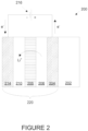
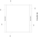
- the electrochromic device includes a substrate 102, a conductive layer (CL) 104, an electrochromic layer (EC) 106 (sometimes also referred to as a cathodically coloring layer), an ion conducting layer (IC) 108, a counter electrode layer (CE) 110 (sometimes also referred to as an anodically coloring layer), and a conductive layer (CL) 114.
- Elements 104, 106, 108, 110, and 114 are collectively referred to as an electrochromic stack 120.
- a voltage source 116 operable to apply an electric potential across the electrochromic stack 120 effects the transition of the electrochromic device from, e.g., a bleached state to a colored state.
- the order of layers is reversed with respect to the substrate. That is, the layers are in the following order: substrate, conductive layer, counter electrode layer, ion conducting layer, electrochromic material layer, conductive layer.
- a transition between a bleached state and colored state is non-limiting and suggests only one example, among many, of an electrochromic transition that may be implemented. Unless otherwise specified herein, whenever reference is made to a bleached-colored transition, the corresponding device or process encompasses other optical state transitions such nonreflective-reflective, transparent-opaque, etc. Further the term “bleached” refers to an optically neutral state, e.g., uncolored, transparent or translucent. Still further, unless specified otherwise herein, the "color" of an electrochromic transition is not limited to any particular wavelength or range of wavelengths. As understood by those of skill in the art, the choice of appropriate electrochromic and counter electrode materials governs the relevant optical transition.
- the electrochromic device reversibly cycles between a bleached state and a colored state.
- a potential is applied to the electrochromic stack 120 such that available ions in the stack that can cause the electrochromic material 106 to be in the colored state reside primarily in the counter electrode 110.
- the potential on the electrochromic stack is reversed, the ions are transported across the ion conducting layer 108 to the electrochromic material 106 and cause the material to enter the colored state.
- all of the materials making up electrochromic stack 120 are inorganic, solid (i.e., in the solid state), or both inorganic and solid. Because organic materials tend to degrade over time, inorganic materials offer the advantage of a reliable electrochromic stack that can function for extended periods of time. Materials in the solid state also offer the advantage of not having containment and leakage issues, as materials in the liquid state often do.
- Each of the layers in the electrochromic device is discussed in detail, below. It should be understood that any one or more of the layers in the stack may contain some amount of organic material, but in many implementations one or more of the layers contains little or no organic matter. The same can be said for liquids that may be present in one or more layers in small amounts. It should also be understood that solid state material may be deposited or otherwise formed by processes employing liquid components such as certain processes employing sol-gels or chemical vapor deposition.
- voltage source 116 is typically a low voltage electrical source and may be configured to operate in conjunction with radiant and other environmental sensors. Voltage source 116 may also be configured to interface with an energy management system, such as a computer system that controls the electrochromic device according to factors such as the time of year, time of day, and measured environmental conditions. Such an energy management system, in conjunction with large area electrochromic devices (i.e., an electrochromic window), can dramatically lower the energy consumption of a building.
- an energy management system in conjunction with large area electrochromic devices (i.e., an electrochromic window) can dramatically lower the energy consumption of a building.
- any material having suitable optical, electrical, thermal, and mechanical properties may be used as substrate 102.
- substrates include, for example, glass, plastic, and mirror materials.
- Suitable plastic substrates include, for example acrylic, polystyrene, polycarbonate, allyl diglycol carbonate, SAN (styrene acrylonitrile copolymer), poly(4-methyl-1-pentene), polyester, polyamide, etc.
- a plastic substrate is used, it is preferably barrier protected and abrasion protected using a hard coat of, for example, a diamond-like protection coating, a silica/silicone anti-abrasion coating, or the like, such as is well known in the plastic glazing art.
- Suitable glasses include either clear or tinted soda lime glass, including soda lime float glass.
- the glass may be tempered or untempered.
- the optical transmittance (i.e., the ratio of transmitted radiation or spectrum to incident radiation or spectrum) of substrate 102 is about 40 to 95%, e.g., about 90-92%.
- the substrate may be of any thickness, as long as it has suitable mechanical properties to support the electrochromic stack 120. While the substrate 102 may be of any size, in some embodiments, it is about 0.01 mm to 10 mm thick, preferably about 3 mm to 9 mm thick.
- the substrate is architectural glass.
- Architectural glass is glass that is used as a building material.
- Architectural glass is typically used in commercial buildings, but may also be used in residential buildings, and typically, though not necessarily, separates an indoor environment from an outdoor environment.
- architectural glass is at least 20 inches by 20 inches, and can be much larger, e.g., as large as about 72 inches by 120 inches.
- Architectural glass is typically at least about 2 mm thick.
- Architectural glass that is less than about 3.2 mm thick cannot be tempered.
- the substrate may still be tempered even after the electrochromic stack has been fabricated on the substrate.
- the substrate is a soda lime glass from a tin float line.
- the percent transmission over the visible spectrum of an architectural glass substrate is generally greater than 80% for neutral substrates, but it could be lower for colored substrates.
- the percent transmission of the substrate over the visible spectrum is at least about 90% (e.g., about 90-92%).
- the visible spectrum is the spectrum that a typical human eye will respond to, generally about 380 nm (purple) to about 780 nm (red).
- the glass has a surface roughness of between about 10 and 30 nm.
- conductive layer 104 On top of substrate 102 is conductive layer 104.
- one or both of the conductive layers 104 and 114 is inorganic and/or solid.
- Conductive layers 104 and 114 may be made from a number of different materials, including conductive oxides, thin metallic coatings, conductive metal nitrides, and composite conductors.
- conductive layers 104 and 114 are transparent at least in the range of wavelengths where electrochromism is exhibited by the electrochromic layer.
- Transparent conductive oxides include metal oxides and metal oxides doped with one or more metals.
- metal oxides and doped metal oxides examples include indium oxide, indium tin oxide, doped indium oxide, tin oxide, doped tin oxide, zinc oxide, aluminum zinc oxide, doped zinc oxide, ruthenium oxide, doped ruthenium oxide and the like. Since oxides are often used for these layers, they are sometimes referred to as "transparent conductive oxide” (TCO) layers. Thin metallic coatings that are substantially transparent may also be used. Examples of metals used for such thin metallic coatings include transition metals including gold, platinum, silver, aluminum, nickel alloy, and the like. Thin metallic coatings based on silver, well known in the glazing industry, are also used.
- conductive nitrides examples include titanium nitrides, tantalum nitrides, titanium oxynitrides, and tantalum oxynitrides.
- the conductive layers 104 and 114 may also be composite conductors. Such composite conductors may be fabricated by placing highly conductive ceramic and metal wires or conductive layer patterns on one of the faces of the substrate and then over-coating with transparent conductive materials such as doped tin oxides or indium tin oxide. Ideally, such wires should be thin enough as to be invisible to the naked eye (e.g., about 100 ⁇ m or thinner).
- commercially available substrates such as glass substrates contain a transparent conductive layer coating.
- Such products may be used for both substrate 102 and conductive layer 104.
- Examples of such glasses include conductive layer coated glasses sold under the trademark TEC Glass TM by Pilkington, of Toledo, Ohio and SUNGATE TM 300 and SUNGATE TM 500 by PPG Industries of Pittsburgh, Pennsylvania.
- TEC Glass TM is a glass coated with a fluorinated tin oxide conductive layer.
- the same conductive layer is used for both conductive layers (i.e., conductive layers 104 and 114 ).
- different conductive materials are used for each conductive layer 104 and 114.
- TEC Glass TM is used for substrate 102 (float glass) and conductive layer 104 (fluorinated tin oxide) and indium tin oxide is used for conductive layer 114.
- TEC Glass TM there is a sodium diffusion barrier between the glass substrate 102 and TEC conductive layer 104.
- the composition of a conductive layer should be chosen or tailored based on the composition of an adjacent layer (e.g., electrochromic layer 106 or counter electrode layer 110 ) in contact with the conductive layer.
- an adjacent layer e.g., electrochromic layer 106 or counter electrode layer 110
- conductivity is a function of the number of oxygen vacancies in the conductive layer material, and the number of oxygen vacancies in the metal oxide is impacted by the composition of the adjacent layer.
- Selection criteria for a conductive layer may also include the material's electrochemical stability and ability to avoid oxidation or more commonly reduction by a mobile ion species.
- the function of the conductive layers is to spread an electric potential provided by voltage source 116 over surfaces of the electrochromic stack 120 to interior regions of the stack, with very little ohmic potential drop.
- the electric potential is transferred to the conductive layers though electrical connections to the conductive layers.
- bus bars one in contact with conductive layer 104 and one in contact with conductive layer 114, provide the electric connection between the voltage source 116 and the conductive layers 104 and 114.
- the conductive layers 104 and 114 may also be connected to the voltage source 116 with other conventional means.
- the thickness of conductive layers 104 and 114 is between about 5 nm and about 10,000 nm. In some embodiments, the thickness of conductive layers 104 and 114 are between about 10 nm and about 1,000 nm. In other embodiments, the thickness of conductive layers 104 and 114 are between about 10 nm and about 500 nm. In some embodiments where TEC Glass TM is used for substrate 102 and conductive layer 104, the conductive layer is about 400 nm thick. In some embodiments where indium tin oxide is used for conductive layer 114, the conductive layer is about 100 nm to 400 nm thick (280 nm in one embodiment).
- the conductive layers 104 and 114 are as thin as possible to increase transparency and to reduce cost.
- conductive layers are substantially crystalline.
- conductive layers are crystalline with a high fraction of large equiaxed grains
- the thickness of the each conductive layer 104 and 114 is also substantially uniform. Smooth layers (i.e., low roughness, Ra) of the conductive layer 104 are desirable so that other layers of the electrochromic stack 120 are more compliant.
- a substantially uniform conductive layer varies by no more than about ⁇ 10% in each of the aforementioned thickness ranges. In another embodiment, a substantially uniform conductive layer varies by no more than about ⁇ 5% in each of the aforementioned thickness ranges. In another embodiment, a substantially uniform conductive layer varies by no more than about ⁇ 2% in each of the aforementioned thickness ranges.
- the sheet resistance (R s ) of the conductive layers is also important because of the relatively large area spanned by the layers.
- the sheet resistance of conductive layers 104 and 114 is about 5 to 30 Ohms per square. In some embodiments, the sheet resistance of conductive layers 104 and 114 is about 15 Ohms per square. In general, it is desirable that the sheet resistance of each of the two conductive layers be about the same. In one embodiment, the two layers each have a sheet resistance of about 10-15 Ohms per square.
- electrochromic layer 106 Overlaying conductive layer 104 is electrochromic layer 106.
- electrochromic layer 106 is inorganic and/or solid, in typical embodiments inorganic and solid.
- the electrochromic layer may contain any one or more of a number of different electrochromic materials, including metal oxides.
- Such metal oxides include tungsten oxide (WO 3 ), molybdenum oxide (MoOs), niobium oxide (Nb 2 O 5 ), titanium oxide (TiO 2 ), copper oxide (CuO), iridium oxide (Ir 2 O 3 ), chromium oxide (Cr 2 O 3 ), manganese oxide (Mn 2 O 3 ), vanadium oxide (V 2 O 5 ), nickel oxide (Ni 2 O 3 ), cobalt oxide (Co 2 O 3 ) and the like.
- the metal oxide is doped with one or more dopants such as lithium, sodium, potassium, molybdenum, vanadium, titanium, and/or other suitable metals or compounds containing metals. Mixed oxides (e.g., W-Mo oxide, W-V oxide) are also used in certain embodiments.
- An electrochromic layer 106 comprising a metal oxide is capable of receiving ions transferred from counter electrode layer 110.
- tungsten oxide or doped tungsten oxide is used for electrochromic layer 106.
- the electrochromic layer is made substantially of WO x , where " x " refers to an atomic ratio of oxygen to tungsten in the electrochromic layer, and x is between about 2.7 and 3.5. It has been suggested that only sub-stoichiometric tungsten oxide exhibits electrochromism; i.e., stoichiometric tungsten oxide, WO 3 , does not exhibit electrochromism. In a more specific embodiment, WO x , where x is less than 3.0 and at least about 2.7 is used for the electrochromic layer.
- the electrochromic layer is WO x , where x is between about 2.7 and about 2.9.
- Techniques such as Rutherford Backscattering Spectroscopy (RBS) can identify the total number of oxygen atoms which include those bonded to tungsten and those not bonded to tungsten.
- tungsten oxide layers where x is 3 or greater exhibit electrochromism, presumably due to unbound excess oxygen along with sub-stoichiometric tungsten oxide.
- the tungsten oxide layer has stoichiometric or greater oxygen, where x is 3.0 to about 3.5.
- the tungsten oxide is crystalline, nanocrystalline, or amorphous. In some embodiments, the tungsten oxide is substantially nanocrystalline, with grain sizes, on average, from about 5 nm to 50 nm (or from about 5 nm to 20 nm), as characterized by transmission electron microscopy (TEM).
- the tungsten oxide morphology may also be characterized as nanocrystalline using x-ray diffraction (XRD); XRD.
- XRD x-ray diffraction
- nanocrystalline electrochromic tungsten oxide may be characterized by the following XRD features: a crystal size of about 10 to 100 nm (e.g., about 55nm.
- nanocrystalline tungsten oxide may exhibit limited long range order, e.g., on the order of several (about 5 to 20) tungsten oxide unit cells.
- the thickness of the electrochromic layer 106 depends on the electrochromic material selected for the electrochromic layer. In some embodiments, the electrochromic layer 106 is about 50 nm to 2,000 nm, or about 200 nm to 700 nm. In some embodiments, the electrochromic layer is about 300 nm to about 500 nm.
- the thickness of the electrochromic layer 106 is also substantially uniform. In one embodiment, a substantially uniform electrochromic layer varies only about ⁇ 10% in each of the aforementioned thickness ranges. In another embodiment, a substantially uniform electrochromic layer varies only about ⁇ 5% in each of the aforementioned thickness ranges. In another embodiment, a substantially uniform electrochromic layer varies only about ⁇ 3% in each of the aforementioned thickness ranges.
- the colorization (or change in any optical property - e.g., absorbance, reflectance, and transmittance) of the electrochromic material is caused by reversible ion insertion into the material (e.g., intercalation) and a corresponding injection of a charge balancing electron.
- a charge balancing electron typically some fraction of the ion responsible for the optical transition is irreversibly bound up in the electrochromic material.
- suitable ions include lithium ions (Li + ) and hydrogen ions (H + ) (i.e., protons). In some cases, however, other ions will be suitable.
- lithium ions are used to produce the electrochromic phenomena. Intercalation of lithium ions into tungsten oxide (WO 3-y (0 ⁇ y ⁇ ⁇ 0.3)) causes the tungsten oxide to change from transparent (bleached state) to blue (colored state).
- ion conducting layer 108 overlays electrochromic layer 106.
- counter electrode layer 110 is inorganic and/or solid.
- the counter electrode layer may comprise one or more of a number of different materials that are capable of serving as reservoirs of ions when the electrochromic device is in the bleached state.
- the counter electrode layer transfers some or all of the ions it holds to the electrochromic layer, changing the electrochromic layer to the colored state. Concurrently, the counter electrode layer colors with the loss of ions.
- suitable materials for the counter electrode layer include a base anodically coloring electrochromic material and one or more additive materials.
- the base anodically coloring material may be, for example, cobalt oxide, chromium oxide, iron oxide, iridium oxide, manganese oxide, nickel oxide, rhodium oxide, ruthenium oxide, vanadium oxide, and any combination thereof.
- the base anodically coloring electrochromic material includes a material selected from the group consisting of chromium oxide, manganese oxide, iron oxide, cobalt oxide, nickel oxide, rhodium oxide, and iridium oxide.
- the base anodically coloring electrochromic material is selected from the group consisting of chromium oxide, manganese oxide, nickel oxide, rhodium oxide, and iridium oxide. In another example, the base anodically coloring electrochromic material includes nickel oxide and/or iridium oxide.
- the additive is selected from the group consisting of silver (Ag), arsenic (As), boron (B), cadmium (Cd), europium (Eu), gallium (Ga), gadolinium (Gd), germanium (Ge), mercury (Hg), osmium (Os), lead (Pb), palladium (Pd), promethium (Pm), polonium (Po), platinum (Pt), radium (Ra), terbium (Tb), technetium (Tc), thorium (Th), thallium (Tl), and combinations thereof.
- the additive is selected from the group consisting of Ga, Gd, Ge, and combinations thereof.
- the additive may include at least one of Ga, Gd, and Ge.
- the additive may include Ge.
- germanium/germanium oxide show a high optical band gap.
- the concentration of the additive metal material may be less than about 50% atomic, less than about 25% atomic, less than about 10% atomic, less than about 5% atomic, less than about 2% atomic, or less than about 1% atomic.
- the additional material should be added at an amount/concentration sufficient to maintain the anodic coloring properties of the electrode.
- the proper balance between the base anodically coloring electrochromic material and the additive depends on the particular materials being used, though one of ordinary skill in the art is readily capable of determining appropriate concentrations to maintain the overall anodically coloring property of the counter electrode.
- a halogen i.e., one or more of fluorine (F), chlorine (Cl), bromine (Br), iodine (I), and astatine (As)
- F fluorine
- Cl chlorine
- Br bromine
- I iodine
- As astatine
- the counter electrode layer may include nickel oxide in combination with an additive in certain cases.
- Example materials for the counter electrode layer in this case may include nickel silver oxide, nickel arsenic oxide, nickel boron oxide, nickel cadmium oxide, nickel europium oxide, nickel gadolinium oxide, nickel gallium oxide, nickel germanium oxide, nickel mercury oxide, nickel osmium oxide, nickel lead oxide, nickel palladium oxide, nickel promethium oxide, nickel polonium oxide, nickel platinum oxide, nickel radium oxide, nickel terbium oxide, nickel technetium oxide, nickel thorium oxide, nickel thallium oxide, and combinations thereof.
- the counter electrode layer may include cobalt oxide in combination with an additive.
- Example materials for the counter electrode layer in this case may include cobalt silver oxide, cobalt arsenic oxide, cobalt boron oxide, cobalt cadmium oxide, cobalt europium oxide, cobalt gadolinium oxide, cobalt gallium oxide, cobalt germanium oxide, cobalt mercury oxide, cobalt osmium oxide, cobalt lead oxide, cobalt palladium oxide, cobalt promethium oxide, cobalt polonium oxide, cobalt platinum oxide, cobalt radium oxide, cobalt terbium oxide, cobalt technetium oxide, cobalt thorium oxide, cobalt thallium oxide, and combinations thereof.
- example materials for the counter electrode layer may include chromium silver oxide, chromium arsenic oxide, chromium boron oxide, chromium cadmium oxide, chromium europium oxide, chromium gadolinium oxide, chromium gallium oxide, chromium germanium oxide, chromium mercury oxide, chromium osmium oxide, chromium lead oxide, chromium palladium oxide, chromium promethium oxide, chromium polonium oxide, chromium platinum oxide, chromium radium oxide, chromium terbium oxide, chromium technetium oxide, chromium thorium oxide, chromium thallium oxide, and combinations thereof.
- example materials for the counter electrode layer may include iron silver oxide, iron arsenic oxide, iron boron oxide, iron cadmium oxide, iron europium oxide, iron gadolinium oxide, iron gallium oxide, iron germanium oxide, iron mercury oxide, iron osmium oxide, iron lead oxide, iron palladium oxide, iron promethium oxide, iron polonium oxide, iron platinum oxide, iron radium oxide, iron terbium oxide, iron technetium oxide, iron thorium oxide, iron thallium oxide, and combinations thereof.
- example materials for the counter electrode layer may include iridium silver oxide, iridium arsenic oxide, iridium boron oxide, iridium cadmium oxide, iridium europium oxide, iridium gadolinium oxide, iridium gallium oxide, iridium germanium oxide, iridium mercury oxide, iridium osmium oxide, iridium lead oxide, iridium palladium oxide, iridium promethium oxide, iridium polonium oxide, iridium platinum oxide, iridium radium oxide, iridium terbium oxide, iridium technetium oxide, iridium thorium oxide, iridium thallium oxide, and combinations thereof.
- example materials for the counter electrode layer may include manganese silver oxide, manganese arsenic oxide, manganese boron oxide, manganese cadmium oxide, manganese europium oxide, manganese gadolinium oxide, manganese gallium oxide, manganese germanium oxide, manganese mercury oxide, manganese osmium oxide, manganese lead oxide, manganese palladium oxide, manganese promethium oxide, manganese polonium oxide, manganese platinum oxide, manganese radium oxide, manganese terbium oxide, manganese technetium oxide, manganese thorium oxide, manganese thallium oxide, and combinations thereof.
- example materials for the counter electrode layer may include rhodium silver oxide, rhodium arsenic oxide, rhodium boron oxide, rhodium cadmium oxide, rhodium europium oxide, rhodium gadolinium oxide, rhodium gallium oxide, rhodium germanium oxide, rhodium mercury oxide, rhodium osmium oxide, rhodium lead oxide, rhodium palladium oxide, rhodium promethium oxide, rhodium polonium oxide, rhodium platinum oxide, rhodium radium oxide, rhodium terbium oxide, rhodium technetium oxide, rhodium thorium oxide, rhodium thallium oxide, and combinations thereof.
- example materials for the counter electrode layer may include ruthenium silver oxide, ruthenium arsenic oxide, ruthenium boron oxide, ruthenium cadmium oxide, ruthenium europium oxide, ruthenium gadolinium oxide, ruthenium gallium oxide, ruthenium germanium oxide, ruthenium mercury oxide, ruthenium osmium oxide, ruthenium lead oxide, ruthenium palladium oxide, ruthenium promethium oxide, ruthenium polonium oxide, ruthenium platinum oxide, ruthenium radium oxide, ruthenium terbium oxide, ruthenium technetium oxide, ruthenium thorium oxide, ruthenium thallium oxide, and combinations thereof.
- example materials for the counter electrode layer may include vanadium silver oxide, vanadium arsenic oxide, vanadium boron oxide, vanadium cadmium oxide, vanadium europium oxide, vanadium gadolinium oxide, vanadium gallium oxide, vanadium germanium oxide, vanadium mercury oxide, vanadium osmium oxide, vanadium lead oxide, vanadium palladium oxide, vanadium promethium oxide, vanadium polonium oxide, vanadium platinum oxide, vanadium radium oxide, vanadium terbium oxide, vanadium technetium oxide, vanadium thorium oxide, vanadium thallium oxide, and combinations thereof.
- the counter electrode layer may include one or more, in some cases two or more, of the materials listed in the previous paragraphs.
- nickel germanium oxide may be combined with iridium gallium oxide, etc.
- counter electrode examples include, but are not limited to, nickel oxide, nickel tungsten oxide, nickel vanadium oxide, nickel chromium oxide, nickel aluminum oxide, nickel manganese oxide, nickel magnesium oxide, chromium oxide, iron oxide, cobalt oxide, rhodium oxide, iridium oxide, manganese oxide.
- the materials e.g., metal and oxygen
- counter electrode layer 110 contains the ions used to produce the electrochromic phenomenon in the electrochromic material when the electrochromic material is in the bleached state, the counter electrode preferably has high transmittance and a neutral color when it holds significant quantities of these ions.
- nickel-tungsten oxide is used in the counter electrode layer along with an additive listed above.
- the amount of nickel present in the nickel-tungsten oxide can be up to about 90% by weight of the nickel-tungsten oxide.
- the mass ratio of nickel to tungsten in the nickel-tungsten oxide is between about 4:6 and 6:4 (e.g., about 1:1).
- the NiWO is between about 15% (atomic) Ni and about 60% Ni; between about 10% W and about 40% W; between about 30% O and about 75% O; and includes one or more additives as described herein.
- the NiWO is between about 30% (atomic) Ni and about 45% Ni; between about 10% W and about 25% W; between about 35% O and about 50% O; and includes one or more additives as described herein.
- the counter electrode layer When charge is removed from a counter electrode 110 (i.e., ions are transported from the counter electrode 110 to the electrochromic layer 106 ), the counter electrode layer will turn from a transparent state to a tinted state. For instance, a nickel tungsten oxide counter electrode 110 will switch from a transparent state to a brown state. Other counter electrode materials may exhibit different colors in their tinted states and/or may be relatively more transparent in their clear states compared to a nickel tungsten oxide counter electrode.
- the counter electrode morphology may be crystalline, nanocrystalline, or amorphous.
- the counter electrode material is amorphous or substantially amorphous.
- Substantially amorphous nickel-tungsten oxide counter electrodes have been found to perform better, under some conditions, in comparison to their crystalline counterparts.
- the amorphous state of the nickel-tungsten oxide may be obtained though the use of certain processing conditions, described below. While not wishing to be bound to any theory or mechanism, it is believed that amorphous nickel-tungsten oxide is produced by relatively higher energy atoms in the sputtering process.
- Higher energy atoms are obtained, for example, in a sputtering process with higher target powers, lower chamber pressures (i.e., higher vacuum), and smaller source to substrate distances. Under the described process conditions, higher density films, with better stability under UV/heat exposure are produced.
- the counter electrode morphology may include microcrystalline, nanocrystalline and/or amorphous phases.
- the counter electrode may be, e.g., a material with an amorphous matrix having nanocrystals distributed throughout.
- the nanocrystals constitute about 50% or less of the counter electrode material, about 40% or less of the counter electrode material, about 30% or less of the counter electrode material, about 20% or less of the counter electrode material or about 10% or less of the counter electrode material (by weight or by volume depending on the embodiment).
- the nanocrystals have a maximum diameter of less than about 50 nm, in some cases less than about 25 nm, less than about 10 nm, or less than about 5 nm.
- the nanocrystals have a mean diameter of about 50 nm or less, or about 10 nm or less, or about 5 nm or less (e.g., about 1-10 nm). In certain embodiments, it is desirable to have a nanocrystal size distribution where at least about 50% of the nanocrystals have a diameter within 1 standard deviation of the mean nanocrystal diameter, for example where at least about 75% of the nanocrystals have a diameter within 1 standard deviation of the mean nanocrystal diameter or where at least about 90% of the nanocrystals have a diameter within 1 standard deviation of the mean nanocrystal diameter.
- the additive may form a host matrix in which domains of the base anodically coloring material may be found.
- the host matrix is substantially amorphous.
- the only crystalline structures in the counter electrode are formed from the base anodically coloring electrochromic material, in, e.g., oxide form.
- the additives may contribute to forming an amorphous host matrix that is not substantially crystalline, but which incorporates domains (e.g., nanocrystals in some cases) of the base anodically coloring electrochromic material.
- the additive and the anodically coloring base material together form a chemical compound with covalent and/or ionic bonding.
- the compound may be crystalline, amorphous, or any combination thereof.
- the anodically coloring base material forms a host matrix in which domains of the additive exist as discrete phases or pockets.
- the thickness of the counter electrode is about 50 nm about 650 nm. In some embodiments, the thickness of the counter electrode is about 100 nm to about 400 nm, preferably in the range of about 200 nm to 300 nm.
- the thickness of the counter electrode layer 110 is also substantially uniform. In one embodiment, a substantially uniform counter electrode layer varies only about ⁇ 10% in each of the aforementioned thickness ranges. In another embodiment, a substantially uniform counter electrode layer varies only about ⁇ 5% in each of the aforementioned thickness ranges. In another embodiment, a substantially uniform counter electrode layer varies only about ⁇ 3% in each of the aforementioned thickness ranges.
- the amount of ions held in the counter electrode layer during the bleached state (and correspondingly in the electrochromic layer during the colored state) and available to drive the electrochromic transition depends on the composition of the layers as well as the thickness of the layers and the fabrication method. Both the electrochromic layer and the counter electrode layer are capable of supporting available charge (in the form of lithium ions and electrons) in the neighborhood of several tens of millicoulombs per square centimeter of layer surface area.
- the charge capacity of an electrochromic film is the amount of charge that can be loaded and unloaded reversibly per unit area and unit thickness of the film by applying an external voltage or potential.
- the WO 3 layer has a charge capacity of between about 30 and about 150 mC/cm 2 /micron.
- the WO 3 layer has a charge capacity of between about 50 and about 100 mC/cm 2 /micron.
- a NiWO layer including an additive listed above has a charge capacity of between about 75 and about 200 mC/cm 2 /micron.
- the NiWO layer (with an additive listed above) has a charge capacity of between about 100 and about 150 mC/cm 2 /micron.
- Ion conducting layer 108 serves as a medium through which ions are transported (in the manner of an electrolyte) when the electrochromic device transforms between the bleached state and the colored state.
- ion conducting layer 108 is highly conductive to the relevant ions for the electrochromic and the counter electrode layers, but has sufficiently low electron conductivity that negligible electron transfer takes place during normal operation.
- a thin ion conducting layer with high ionic conductivity permits fast ion conduction and hence fast switching for high performance electrochromic devices.
- the ion conducting layer 108 is inorganic and/or solid.
- the ion conductor layer When fabricated from a material and in a manner that produces relatively few defects, the ion conductor layer can be made very thin to produce a high performance device.
- the ion conductor material has an ionic conductivity of between about 10 8 Siemens/cm or ohm -1 cm -1 and about 10 9 Siemens/cm or ohm -1 cm -1 and an electronic resistance of about 10 11 ohms-cm.
- Suitable ion conducting layers include silicates, silicon oxides, tungsten oxides, tantalum oxides, niobium oxides, and borates.
- the silicon oxides include silicon-aluminum-oxide. These materials may be doped with different dopants, including lithium. Lithium doped silicon oxides include lithium silicon-aluminum-oxide.
- the ion conducting layer comprises a silicate-based structure.
- suitable ion conductors particularly adapted for lithium ion transport include, but are not limited to, lithium silicate, lithium aluminum silicate, lithium aluminum borate, lithium aluminum fluoride, lithium borate, lithium nitride, lithium zirconium silicate, lithium niobate, lithium borosilicate, lithium phosphosilicate, and other such lithium-based ceramic materials, silicas, or silicon oxides, including lithium silicon-oxide.
- Any material, however, may be used for the ion conducting layer 108 provided it can be fabricated with low defectivity and it allows for the passage of ions between the counter electrode layer 110 to the electrochromic layer 106 while substantially preventing the passage of electrons.
- the ion conducting layer is crystalline, nanocrystalline, or amorphous. Typically, the ion conducting layer is amorphous. In another embodiment, the ion conducting layer is nanocrystalline. In yet another embodiment, the ion conducting layer is crystalline.
- a silicon-aluminum-oxide (SiAlO) is used for the ion conducting layer 108.
- a silicon/aluminum target used to fabricate the ion conductor layer via sputtering contains between about 6 and about 20 atomic percent aluminum. This defines the ratio of silicon to aluminum in the ion conducting layer.
- the silicon-aluminum-oxide ion conducting layer 108 is amorphous.
- the thickness of the ion conducting layer 108 may vary depending on the material. In some embodiments, the ion conducting layer 108 is about 5 nm to 100 nm thick, preferably about 10 nm to 60 nm thick. In some embodiments, the ion conducting layer is about 15 nm to 40 nm thick or about 25 nm to 30 nm thick.
- the thickness of the ion conducting layer is also substantially uniform. In one embodiment, a substantially uniform ion conducting layer varies by not more than about ⁇ 10% in each of the aforementioned thickness ranges. In another embodiment, a substantially uniform ion conducting layer varies by not more than about ⁇ 5% in each of the aforementioned thickness ranges. In another embodiment, a substantially uniform ion conducting layer varies by not more than about ⁇ 3% in each of the aforementioned thickness ranges.
- Ions transported across the ion conducting layer between the electrochromic layer and the counter electrode layer serve to effect a color change in the electrochromic layer (i.e., change the electrochromic device from the bleached state to the colored state).
- ions include lithium ions (Li + ) and hydrogen ions (H + ) (i.e., protons).
- other ions may be employed in certain embodiments. These include deuterium ions (D + ), sodium ions (Na + ), potassium ions (K + ), calcium ions (Ca ++ ), barium ions (Ba ++ ), strontium ions (Sr ++ ), and magnesium ions (Mg ++ ).
- the ion conducting layer 108 should have very few defects. Among other problems, defects in the ion conducting layer may result in short circuits between the electrochromic layer and the counter electrode layer (described in more detail below in relation to Figure 4 ). A short circuit occurs when electrical communication is established between oppositely charged conductive layers, e.g. a conductive particle makes contact with each of two conductive and electrically charged layers (as opposed to a "pin hole" which is a defect which does not create a short circuit between oppositely charged conductive layers).
- the ion conducting layer is preferably as thin as possible, without any shorts between the electrochromic layer and the counter electrode layer.
- low defectivity in the ion conducting layer 108 allows for a thinner ion conducting layer 108. Ion transport between the electrochromic layer and the counter electrode layer with electrochemical cycling is faster when using a thin ion conducting layer.
- the defectivity criteria specified herein may apply to any specific layer (ion conducting layer or otherwise) in the stack or to the stack as a whole or to any portion thereof. Defectivity criteria will be further discussed below.
- the electrochromic device 100 may include one or more additional layers (not shown) such as one or more passive layers. Passive layers used to improve certain optical properties may be included in electrochromic device 100. Passive layers for providing moisture or scratch resistance may also be included in the electrochromic device 100. For example, the conductive layers may be treated with anti-reflective or protective oxide or nitride layers. Other passive layers may serve to hermetically seal the electrochromic device 100.
- FIG. 2 is a schematic cross-section of an electrochromic device in a bleached state (or transitioning to a bleached state).
- the electrochromic device 200 includes a tungsten oxide electrochromic layer (EC) 206 and a counter electrode layer (CE) 210 as described herein.
- the tungsten oxide electrochromic layer 206 has a nanocrystalline, or substantially nanocrystalline, morphology.
- the counter electrode layer 210 has an amorphous, or substantially amorphous, morphology.
- the weight percent ratio of tungsten to nickel in the counter electrode is about 0.40 - 0.60
- the electrochromic device 200 also includes substrate 202, conductive layer (CL) 204, ion conducting layer (IC) 208, and conductive layer (CL) 214.
- the substrate 202 and conductive layer 204 together comprise a TEC-Glass TM .
- the electrochromic devices described herein, such as those of Figure 2 often find beneficial application in architectural glass.
- the substrate 202 is of the dimensions such that it may be classified as architectural glass.
- the conductive layer 214 is indium tin oxide (ITO).
- the ion conducting layer 208 is a silicon-aluminum-oxide.
- the voltage source 216 is configured to apply a potential to electrochromic stack 220 through suitable connections (e.g., bus bars) to conductive layers 204 and 214. In some embodiments, the voltage source is configured to apply a potential of about 2 volts in order to drive a transition of the device from one optical state to another.
- the polarity of the potential as shown in Figure 2 is such that the ions (lithium ions in this example) primarily reside in the counter electrode layer 210.
- the ratio of the electrochromic layer thickness to the counter electrode layer thickness may be about 1.7:1 to 2.3:1 (e.g., about 2:1).
- the electrochromic tungsten oxide layer is about 200 nm to 700 nm thick.
- the electrochromic tungsten oxide layer is about 400 nm to 500 nm thick.
- the counter electrode layer is about 100 nm to 350 nm thick. In further embodiments, the counter electrode layer is about 200 nm to 250 nm thick.
- the counter electrode layer is about 240 nm thick.
- the silicon-aluminum-oxide ion conducting layer 208 is about 10 nm to 100 nm thick. In further embodiments, the silicon-aluminum-oxide ion conducting layer is about 20 nm to 50 nm thick.
- electrochromic materials may contain blind charge.
- the blind charge in an electrochromic material is the charge (e.g., negative charge in the case of tungsten oxide electrochromic material) that exists in the material as fabricated, absent compensation by oppositely charged ions or other charge carriers.
- the magnitude of the blind charge depends upon the excess oxygen concentration during sputtering of the tungsten oxide.
- blind charge must be compensated before the ions employed to transform the electrochromic material can effectively change an optical property of the electrochromic material. Without prior compensation of the blind charge, ions supplied to an electrochromic material will irreversibly incorporate in the material and have no effect on the optical state of the material.
- an electrochromic device is typically provided with ions, such as lithium ions or protons, in an amount sufficient both to compensate the blind charge and to provide a supply of ions for reversibly switching the electrochromic material between two optical states.
- ions such as lithium ions or protons
- charge is lost during the first electrochemical cycle in compensating blind charge.
- lithium is present in the electrochromic stack 220 in an amount sufficient to compensate the blind charge in the electrochromic layer 206 and then an additional amount of about 1.5 to 2.5 times the amount used to compensate the blind charge (by mass) in the stack (initially in the counter electrode layer 210 for example). That is, there is about 1.5 to 2.5 times the amount of lithium needed to compensate the blind charge that is provided for reversible cycling between the electrochromic layer 206 and the counter electrode layer 210 in the electrochromic stack 220. In some embodiments, there are enough lithium in the electrochromic stack 220 to compensate the blind charge in the electrochromic layer 206 and then about two times this amount (by mass) in the counter electrode layer 210 or elsewhere in the stack.
- FIG 3 is a schematic cross-section of electrochromic device 200 shown in Figure 2 but in a colored state (or transitioning to a colored state).
- the polarity of voltage source 216 is reversed, so that the electrochromic layer is made more negative to accept additional lithium ions, and thereby transition to the colored state.
- lithium ions are transported across the ion conducting layer 208 to the tungsten oxide electrochromic layer 206.
- the tungsten oxide electrochromic layer 206 is shown in the colored state.
- the counter electrode 210 is also shown in the colored state. As explained, the counter electrode material becomes progressively more opaque as it gives up (deintercalates) lithium ions.
- there is a synergistic effect where the transition to colored states for both layers 206 and 210 are additive toward reducing the amount of light transmitted through the stack and substrate.
- electrochromic devices of the types described above are very reliable, often substantially more so than counterpart devices of the prior art. Reliability may be characterized by various metrics. Some of these are described in ASTM E2141 - 06 (Standard Test Methods for Assessing the Durability of Absorptive Electrochromic Coatings on Sealed Insulating Glass Units). In some specific cases, the devices are able to cycle between two distinct optical states (e.g., between bleached and colored) over 50,000 times while maintaining a ratio of the bleached T vis to colored T vis (also know as PTR or photopic transmission ratio) of> 4. The longevity of these electrochromic devices makes them suitable for use in applications where the electrochromic devices are expected to be in place for tens of years.
- ASTM E2141 - 06 Standard Test Methods for Assessing the Durability of Absorptive Electrochromic Coatings on Sealed Insulating Glass Units.
- the devices are able to cycle between two distinct optical states (e.g., between bleached and colored) over
- the electrochromic devices in embodiments of the invention are able to cycle between bleached and unbleached states without losing transmissivity in the bleached state and without degradation of the color or other property in the unbleached state.
- the high reliability of an electrochromic device in accordance with embodiments herein described is due in part to a design in which the thickness of the electrochromic layer and/or the thickness of the counter electrode layer in a stack do not substantially change during electrochemical cycling of the electrochromic device from their as deposited, post lithiation thickness (e.g., by no more than about 4%).
- defects refers to a defective point or region of an electrochromic device. Defects may be caused by electrical shorts or by pinholes. Further, defects may be characterized as visible or non-visible. In general, a defect in an electrochromic device does not change optical state (e.g., color) in response to an applied potential that is sufficient to cause non-defective regions of the electrochromic device to color or otherwise change optical state. Often a defect will be manifest as visually discernable anomalies in the electrochromic window or other device. Such defects are referred to herein as "visible" defects.
- a short is a localized electronically conductive pathway spanning the ion conducting layer (e.g., an electronically conductive pathway between the two TCO layers).
- a pinhole is a region where one or more layers of the electrochromic device are missing or damaged so that electrochromism is not exhibited. Pinholes are not electrical shorts.
- Three types of defects are of primary concern: (1) visible pinholes, (2) visible shorts, and (3) non-visible shorts. Typically, though not necessarily, a visible short will have defect dimension of at least about 3 micrometers resulting in a region, e.g.
- a visible pinhole will have a defect dimension of at least about 100 micrometers.
- an electrical short is created by a conductive particle lodging in the ion conducting layer, thereby causing an electronic path between the counter electrode layer and the electrochromic layer or the TCO associated with either one of them.
- a defect is caused by a particle on the substrate (on which the electrochromic stack is fabricated) and such particle causes layer delamination (sometimes called "pop-off') or the layers not to adhere to the substrate. Both types of defects are illustrated below in Figures 4 and 5A - 5C . A delamination or pop-off defect can lead to a short if it occurs before a TCO or associated EC or CE is deposited.
- An electrical short can cause leakage current across the ion conducting layer and result in a potential drop in the vicinity of the short. If the potential drop is of sufficient magnitude it will prevent the electrochromic device from undergoing an electrochromic transition in the vicinity of the short. In the case of a visible short the defect will appear as a light central region (when the device is in the colored state) with a diffuse boundary such that the device gradually darkens with distance from the center of the short. If there are a significant number of electrical shorts (visible or non-visible) concentrated in an area of an electrochromic device, they may collectively impact a broad region of the device whereby the device cannot switch in such region.
- leakage current may result from sources other than short-type defects.
- Such other sources include broad-based leakage across the ion conducting layer and edge defects such as roll off defects as described elsewhere herein and scribe line defects. The emphasis here is on leakage caused only by points of electrical shorting across the ion conducting layer in the interior regions of the electrochromic device.
- FIG 4 is a schematic cross-section of an electrochromic device 400 with a particle in the ion conducting layer causing a localized defect in the device.
- Electrochromic device 400 includes the same components as depicted in Figure 2 for electrochromic device 200. In the ion conducting layer 208 of electrochromic device 400, however, there is a conductive particle 402 or other artifact causing a defect. Conductive particle 402 results in a short between electrochromic layer 206 and counter electrode layer 210.
- This short does not allow the flow of ions between electrochromic layer 206 and counter electrode layer 210, instead allowing electrons to pass locally between the layers, resulting in a transparent region 404 in the electrochromic layer 206 and a transparent region 406 in the counter electrode layer 210 when the remainder of layers 210 and 206 are in the colored state. That is, if electrochromic device 400 is in the colored state, conductive particle 402 renders regions 404 and 406 of the electrochromic device unable to enter into the colored state. Sometimes the defect regions are referred to as "constellations" because they appear as a series of bright spots (or stars) against a dark background (the remainder of the device being in the colored state). Humans will naturally direct their attention to the constellations and often find them distracting or unattractive.
- FIG. 5A is a schematic cross-section of an electrochromic device 500 with a particle 502 or other debris on conductive layer 204 prior to depositing the remainder of the electrochromic stack.
- Electrochromic device 500 includes the same components as electrochromic device 200.
- Particle 502 causes the layers in the electrochromic stack 220 to bulge in the region of particle 502, due to conformal layers 206-210 being deposited sequentially over particle 502 as depicted (in this example, layer 214 has not yet been deposited). While not wishing to be bound by a particular theory, it is believed that layering over such particles, given the relatively thin nature of the layers, can cause stress in the area where the bulges are formed.
- each layer around the perimeter of the bulged region, there can be defects in the layer, e.g. in the lattice arrangement or on a more macroscopic level, cracks or voids.
- defects e.g. in the lattice arrangement or on a more macroscopic level, cracks or voids.
- One consequence of these defects would be, for example, an electrical short between electrochromic layer 206 and counter electrode layer 210 or loss of ion conductivity in layer 208.
- FIG. 5B another consequence of defects caused by particle 502 is called a "pop-off.”
- a portion above the conductive layer 204 in the region of particle 502 breaks loose, carrying with it portions of electrochromic layer 206, ion conducting layer 208, and counter electrode layer 210.
- the "pop-off" is piece 504, which includes particle 502, a portion of electrochromic layer 206, as well as ion conducting layer 208 and counter electrode layer 210.
- the result is an exposed area of conductive layer 204.
- FIG. 5C after pop-off and once conductive layer 214 is deposited, an electrical short is formed where conductive layer 214 comes in contact with conductive layer 204. This electrical short would leave a transparent region in electrochromic device 500 when it is in the colored state, similar in appearance to the defect created by the short described above in relation to Figure 4 .
- Pop-off defects due to particles or debris on substrate 202 or 204 (as described above), on ion conducting layer 208, and on counterelectrode layer 210 may also occur, causing pinhole defects when the electrochromic device is in the colored state. Also, if particle 502 is large enough and does not cause a pop-off, it might be visible when electrochromic device 500 is in the bleached state.
- the electrochromic devices in embodiments of the invention are also scalable to substrates smaller or larger than architectural glass.
- An electrochromic stack can be deposited onto substrates that are a wide range of sizes, up to about 12 inches by 12 inches, or even 80 inches by 120 inches.
- the capability of manufacturing electrochromic devices of 20 by 20 inches allows the manufacture of electrochromic architectural glass for many applications.
- the number of visible pinhole defects is no greater than about 0.04 per square centimeter. In another embodiment, the number of visible pinhole defects is no greater than about 0.02 per square centimeter, and in more specific embodiments, the number of such defects is no greater than about 0.01 per square centimeter.
- the visible short-type defects are individually treated after fabrication to leave short-related pinholes as the only visible defects. In one embodiment, the number of visible short-related pinhole defects is no greater than about 0.005 per square centimeter. In another embodiment, the number of visible short-related pinhole defects is no greater than about 0.003 per square centimeter, and in more specific embodiments, the number of such defects is no greater than about 0.001 per square centimeter.
- the total number of visible defects, pinholes and short-related pinholes created from isolating visible short-related defects is less than about 0.1 defects per square centimeter, in another embodiment less than about 0.08 defects per square centimeter, in another embodiment less than about 0.045 defects per square centimeter (less than about 450 defects per square meter of window).
- the number of non-visible electrical short defects results in leakage currents of less than about 5 ⁇ A/cm 2 at ⁇ 2V bias. These values apply across the entire face of the electrochromic device (i.e., there is no region of the device (anywhere on the device) having a defect density greater than the recited value).
- the electrochromic device has no visible defects greater than about 1.6 mm in diameter (the largest transverse dimension of the defect). In another embodiment, the device has no visible defects greater than about 0.5 mm in diameter, in another embodiment the device has no visible defects greater than about 100 ⁇ m in diameter.
- electrochromic glass is integrated into an insulating glass unit (IGU).
- IGU insulating glass unit
- An insulating glass unit consists of multiple glass panes assembled into a unit, generally with the intention of maximizing the thermal insulating properties of a gas contained in the space formed by the unit while at the same time providing clear vision through the unit.
- Insulating glass units incorporating electrochromic glass would be similar to insulating glass units currently known in the art, except for electrical leads for connecting the electrochromic glass to voltage source. Due to the higher temperatures (due to absorption of radiant energy by an electrochromic glass) that electrochromic insulating glass units may experience, more robust sealants than those used in conventional insulating glass units may be necessary. For example, stainless steel spacer bars, high temperature polyisobutylene (PIB), new secondary sealants, foil coated PIB tape for spacer bar seams, and the like.
- PIB high temperature polyisobutylene
- one aspect of the invention is a method of fabricating an electrochromic stack, as defined in appended claim 1.
- the method includes sequentially depositing on a substrate (i) an electrochromic layer, (ii) an ion conducting layer, and (iii) a counter electrode layer to form a stack in which the ion conducting layer separates the electrochromic layer and the counter electrode layer.
- the sequential deposition employs a single integrated deposition system having a controlled ambient environment in which the pressure, temperature, and/or gas composition are controlled independently of an external environment outside of the integrated deposition system, and the substrate does not leave the integrated deposition system at any time during the sequential deposition of the electrochromic layer, the ion conducting layer, and the counter electrode layer.
- the gas composition may be characterized by the partial pressures of the various components in the controlled ambient environment.
- the controlled ambient environment also may be characterized in terms of the number of particles or particle densities.
- the controlled ambient environment contains fewer than 350 particles (of size 0.1 micrometers or larger) per m 3 .
- the controlled ambient environment meets the requirements of a class 100 clean room (US FED STD 209E).
- the controlled ambient environment meets the requirements of a class 10 clean room (US FED STD 209E).
- the substrate may enter and/or leave the controlled ambient environment in a clean room meeting class 100 or even class 10 requirements.
- this method of fabrication is integrated into a multistep process for making an electrochromic window using architectural glass as the substrate.
- this method of fabrication is integrated into a multistep process for making an electrochromic window using architectural glass as the substrate.
- the following description contemplates the method and its various embodiments in the context of a multistep process for fabricating an electrochromic window, but methods of the invention are not so limited.
- Electrochromic mirrors and other devices may be fabricated using some or all of the operations and approaches described herein.
- Figure 6A is a cross-sectional representation of an electrochromic window device, 600, in accord with a multistep process such as that described in relation to Figure 7A.
- Figure 7A depicts a process flow describing a method, 700, of fabricating an electrochromic window which incorporates electrochromic device 600.
- Figure 6B is a top view of device 600 showing the location of trenches cut into the device. Thus, Figures 6A-B and 7A will be described together.
- One aspect of the description is an electrochromic window including device 600 and another aspect of the description is a method, 700, of fabricating an electrochromic window which includes device 600. Included in the following description are descriptions of Figures 7B - 7E .
- Figures 7B - 7D depict specific methods of fabricating an electrochromic stack which is part of device 600.
- Figure 7E depicts a process flow for a conditioning process used in fabricating, e.g., device 600.
- Figure 6A shows a specific example of an electrochromic device, 600, which is fabricated starting with a substrate made of glass 605 which optionally has a diffusion barrier 610 coating and a first transparent conducting oxide (TCO) coating 615 on the diffusion barrier.
- Method 700 employs a substrate that is, for example, float glass with sodium diffusion barrier and antireflective layers followed by a transparent conductive layer, for example a transparent conductive oxide 615.
- substrates suitable for devices of the invention include glasses sold under the trademarks TEC Glass ® by Pilkington of Toledo, Ohio, and SUNGATE ® 300 and SUNGATE ® 500 by PPG Industries, of Pittsburgh, Pennsylvania.
- the first TCO layer 615 is the first of two conductive layers used to form the electrodes of electrochromic device 600 fabricated on the substrate.
- Method 700 begins with a cleaning process, 705, where the substrate is cleaned to prepare it for subsequent processing.
- a cleaning process 705
- One critical defect is a particle or other contaminant that creates a conductive pathway across the IC layer and thus shorts the device locally causing visually discernable anomalies in the electrochromic window.
- Lisec TM a trade name for a glass washing apparatus and process available from (LISEC Maschinenbau Gmbh of 9.
- Cleaning the substrate may include mechanical scrubbing as well as ultrasonic conditioning to remove unwanted particulates.
- particulates may lead to cosmetic flaws as well as local shorting within the device.
- a first laser scribe process, 710 is performed in order to remove a line of the first TCO layer on the substrate.
- the resulting trench ablates through both the TCO and the diffusion barrier (although in some cases the diffusion barrier is not substantially penetrated).
- Figure 6A depicts this first laser scribe trench, 620.
- a trench is scribed in the substrate across the entire length of one side of the substrate in order to isolate an area of the TCO, near one edge of the substrate, which will ultimately make contact with a first bus bar, 640, used to provide current to a second TCO layer, 630, which is deposited on top of electrochromic (EC) stack 625 (which includes the electrochromic, ion conducting and counter electrode layers as described above).
- EC electrochromic
- FIG. 6B shows schematically (not to scale) the location of trench 620.
- the non-isolated (main) portion of the first TCO layer, on the diffusion barrier ultimately makes contact with a second bus bar, 645.
- Isolation trench 620 may be needed because, in certain embodiments, the method of attaching the first bus bar to the device includes pressing it through the device stack layers after they are laid down (both on the isolated portion of the first TCO layer and the main portion of the first TCO layer).
- the method of attaching the first bus bar to the device includes pressing it through the device stack layers after they are laid down (both on the isolated portion of the first TCO layer and the main portion of the first TCO layer).
- the TCO area isolated by the first laser scribe is typically an area along one edge of the substrate that will ultimately, along with the bus bars, be hidden when incorporated into the integrated glass unit (IGU) and/or window pane, frame or curtain wall.
- the laser or lasers used for the first laser scribe are typically, but not necessarily, pulse-type lasers, for example diode-pumped solid state lasers.
- the laser scribes can be performed using a suitable laser from IPG Photonics (of Oxford Massachusetts), or from Ekspla (of Vilnius Lithuania).
- the laser trench is dug along a side of the substrate from end to end to isolate a portion of the first TCO layer; the depth and width dimensions of trench 620 made via first laser scribe 710 should be sufficient to isolate the first TCO layer from the bulk TCO once the device is subsequently deposited .
- the depth and width of the trench should be sufficient to prevent any remaining particulates to short across the trench.
- the trench is between about 300 nm and 500 nm deep and between about 20 ⁇ m and 50 ⁇ m wide.
- the trench is between about 350 nm and 450 nm deep and between about 30 ⁇ m and 45 ⁇ m wide.
- the trench is about 400 nm deep and about 40 ⁇ m wide.
- the substrate is cleaned again (operation 715 ), typically but not necessarily, using cleaning methods described above. This second cleaning process is performed to remove any debris caused by the first laser scribe. Once cleaning operation 715 is complete, the substrate is ready for deposition of EC stack 625. This is depicted in process flow 700 as process 720.
- the method includes sequentially depositing on a substrate (i) an EC layer, (ii) an IC layer, and (iii) a CE layer to form a stack in which the IC layer separates the EC layer and the CE layer using a single integrated deposition system having a controlled ambient environment in which the pressure and/or gas composition are controlled independently of an external environment outside of the integrated deposition system, and the substrate does not leave the integrated deposition system at any time during the sequential deposition of the EC layer, the IC layer, and the CE layer.
- each of the sequentially deposited layers is physical vapor deposited.
- the layers of the electrochromic device may be deposited by various techniques including physical vapor deposition, chemical vapor deposition, plasma enhanced chemical vapor deposition, and atomic layer deposition, to name a few.
- physical vapor deposition as used herein includes the full range of art understood PVD techniques including sputtering, evaporation, ablation, and the like.
- Figure 7B depicts one embodiment of process 720. First the EC layer is deposited on the substrate, process 722, then the IC layer is deposited, process 724, then the CE layer, process 726. The reverse order of deposition is also an embodiment of the invention, that is, where the CE layer is deposited first, then the IC layer and then the EC layer.
- each of the electrochromic layer, the ion conducting layer, and the counter electrode layer is a solid phase layer. In another embodiment, each of the electrochromic layer, the ion conducting layer, and the counter electrode layer includes only inorganic material.
- any one or more of these layers may be composed of one or more sub-layers, which may have distinct compositions, sizes, morphologies, charge densities, optical properties, etc.
- any one or more of the device layers may have a graded composition or a graded morphology in which the composition or morphology, respectively, changes over at least a portion of the thickness of the layer.
- the concentration of a dopant or charge carrier varies within a given layer, at least as the layer is fabricated.
- the morphology of a layer varies from crystalline to amorphous.
- Such graded composition or morphology may be chosen to impact the functional properties of the device.
- additional layers may be added to the stack.
- a heat spreader layer is interposed between one or both TCO layers and the EC stack.
- a cathodically coloring electrochromic layer and/or an anodically coloring counter electrode layer may be deposited as two distinct sub-layers optionally having different compositions. Certain processing steps (e.g., lithiation) may occur between depositing the sub-layers.
- counter electrode material is deposited in two sub-layers having different compositions. The first sub-layer (closer to the cathodically coloring electrochromic layer) may be anodically coloring, while the second sub-layer (farther away from the cathodically coloring electrochromic layer) may or may not be anodically coloring, or may be more weakly anodically coloring than the first sub-layer.
- the partially fabricated device may be subject to a lithiation operation.
- the second sub-layer may reduce the risk of forming defects.
- the second sub-layer acts as a defect-mitigating layer, and may be more electronically insulating than the first sub-layer.
- the electrochromic devices of the invention utilize ion movement between the electrochromic layer and the counter electrode layer via an ion conducting layer.
- these ions or neutral precursors thereof are introduced to the stack as one or more layers (as described below in more detail in relation to Figures 7C and 7D ) that eventually intercalate into the stack.
- these ions are introduced into the stack concurrently with one or more of the electrochromic layer, the ion conducting layer, and the counter electrode layer.
- lithium is, e.g., sputtered along with the material used to make the one or more of the stack layers or sputtered as part of a material that includes lithium (e.g., by a method employing lithium nickel tungsten oxide, optionally provided with other additives as listed herein).
- the IC layer is deposited via sputtering a lithium silicon aluminum oxide target.
- the Li is cosputtered along with silicon aluminum in order to achieve the desired film.
- depositing the electrochromic layer comprises depositing WO x , e.g. where x is less than 3.0 and at least about 2.7.
- the WO x has a substantially nanocrystalline morphology.
- the electrochromic layer is deposited to a thickness of between about 200 nm and 700 nm.
- depositing the electrochromic layer includes sputtering tungsten from a tungsten containing target. In one such embodiment, a metallic tungsten (or tungsten alloy) target is used.
- the sputter gas is an inert gas (e.g., argon or xenon) with some oxygen containing gas (e.g., molecular or atomic oxygen) present.
- the gas composition contains between about 30% and about 100% oxygen, in another embodiment between about 50% and about 80% oxygen, in yet another embodiment between about 65% and about 75% oxygen.
- the tungsten containing target contains between about 80% and 100% (by weight) tungsten, in another embodiment between about 95% and 100% tungsten, and in yet another embodiment between about 99% and 100% tungsten.
- the gas composition is about 70% oxygen/30% argon and the target is metallic tungsten of a purity of between about 99% and 100%.
- a tungsten oxide W(O) ceramic target is sputtered with, e.g., argon.
- the pressure in the deposition station or chamber in one embodiment, is between about 1 and about 75 mTorr, in another embodiment between about 5 and about 50 mTorr, in another embodiment between about 10 and about 20 mTorr.
- the substrate temperature for process 722 is between about 100°C and about 500°C, in another embodiment between about 100°C and about 300°C, and in another embodiment between about 150°C and about 250°C.
- the substrate temperature may be measured in situ by, e.g., a thermocouple such as an infra-red thermo-couple (IR t/c).
- a thermocouple such as an infra-red thermo-couple (IR t/c).
- the power density used to sputter the EC target is between about 2 Watts/cm 2 and about 50 Watts/cm 2 (determined based on the power applied divided by the surface area of the target); in another embodiment between about 10 Watts/cm 2 and about 20 Watts/cm 2 ; and in yet another embodiment between about 15 Watts/cm 2 and about 20 Watts/cm 2 .
- the power delivered to effect sputtering is provided via direct current (DC). In other embodiments, pulsed DC/AC reactive sputtering is used.
- the frequency is between about 20 kHz and about 400 kHz, in another embodiment between about 20 kHz and about 50 kHz, in yet another embodiment between about 40 kHz and about 50 kHz, in another embodiment about 40 kHz.
- the above conditions may be used in any combination with one another to effect deposition of a high quality tungsten oxide electrochromic layer.
- the distance between the target and the substrate may also be important.
- the distance between the target (cathode or source) to the substrate surface is between about 35 mm and about 150 mm; in another embodiment between about 45 mm and about 130 mm; and in another embodiment between about 70 mm and about 100 mm.
- deposition of the EC layer is described in terms of sputtering from a target, other deposition techniques are employed in some embodiments. For example, chemical vapor deposition, atomic layer deposition, and the like may be employed. Each of these techniques, along with PVD, has its own form of material source as is known to those of skill in the art.
- depositing the ion conducting layer includes depositing a material selected from the group consisting of a tungsten oxide, a tantalum oxide, a niobium oxide, and a silicon aluminum oxide.
- depositing the ion conducting layer includes sputtering a target including between about 2% and 20% by weight of aluminum (remainder silicon) in an oxygen containing environment to produce a layer of silicon aluminum oxide.
- the target is between about 5% and about 10% aluminum in silicon, in another embodiment, between about 7% and about 9% aluminum in silicon.
- the gas composition contains between about 15% and about 70% oxygen, in another embodiment between about 20% and about 50% oxygen, in yet another embodiment between about 25% and about 45% oxygen, in another embodiment about 35% oxygen.
- depositing the ion conducting layer includes depositing the ion conducting layer to a thickness of between about 10 and 100 nm. In yet another embodiment, depositing the ion conducting layer includes depositing the ion conducting layer to a thickness of between about 20 and 50 nm.
- the power density used to sputter the IC target is between about 1 Watts/cm 2 and about 20 Watts/cm 2 (determined based on the power applied divided by the surface area of the target); in another embodiment between about 5 Watts/cm 2 and about 7 Watts/cm 2 ; and in yet another embodiment between about 6 Watts/cm 2 and about 6.5 Watts/cm 2 .
- the power delivered to effect sputtering is provided via direct current (DC). In other embodiments, pulsed DC/AC reactive sputtering is used.
- the frequency is between about 20 kHz and about 400 kHz, in another embodiment between about 20 kHz and about 50 kHz, in yet another embodiment between about 40 kHz and about 50 kHz, in another embodiment about 40 kHz.
- the pressure in the deposition station or chamber in one embodiment, is between about 5 mTorr and about 40 mTorr, in another embodiment between about 10 mTorr and about 30 mTorr, in another embodiment about 20 mTorr.
- the substrate temperature ranges for operation 724 are between about 20°C and about 200°C, in some embodiments between about 20°C and about 150°C, and it yet still other embodiments between about 25°C and about 100°C.
- the above conditions may be used in any combination with one another to effect deposition of a high quality ion conducting layer.
- depositing the counter electrode layer includes depositing a layer of nickel tungsten oxide (NiWO) that includes one or more additives as described above, preferably amorphous NiWO.
- depositing the counter electrode layer includes sputtering a target including about 30 % (by weight) to about 70 % of tungsten in nickel in an oxygen containing environment to produce a layer of nickel tungsten oxide.
- the target is between about 40% and about 60% tungsten in nickel, in another embodiment between about 45% and about 55% tungsten in nickel, and in yet another embodiment about 51% tungsten in nickel.
- the gas composition contains between about 30% and about 100% oxygen, in another embodiment between about 80% and about 100% oxygen, in yet another embodiment between about 95% and about 100% oxygen, in another embodiment about 100% oxygen.
- the additive(s) may be introduced via the sputter target in some cases. In these or other cases, the additive(s) may be introduced via another method, for example through evaporation, which may or may not occur concurrently with sputtering.
- the power density used to sputter the CE target is between about 2 Watts/cm 2 and about 50 Watts/cm 2 (determined based on the power applied divided by the surface area of the target); in another embodiment between about 5 Watts/cm 2 and about 20 Watts/cm 2 ; and in yet another embodiment between about 8 Watts/cm 2 and about 10 Watts/cm 2 , in another embodiment about 8 Watts/cm 2 .
- the power delivered to effect sputtering is provided via direct current (DC). In other embodiments, pulsed DC/AC reactive sputtering is used.
- the frequency is between about 20 kHz and about 400 kHz, in another embodiment between about 20 kHz and about 50 kHz, in yet another embodiment between about 40 kHz and about 50 kHz, in another embodiment about 40 kHz.
- the pressure in the deposition station or chamber in one embodiment, is between about 1 and about 50 mTorr, in another embodiment between about 20 and about 40 mTorr, in another embodiment between about 25 and about 35 mTorr, in another embodiment about 30 mTorr.
- a nickel tungsten oxide NiWO ceramic target (which may or may not include one or more additives as described above) is sputtered with, e.g., argon and oxygen.
- the NiWO is between about 15% (atomic) Ni and about 60% Ni; between about 10% W and about 40% W; and between about 30% O and about 75% O.
- the NiWO is between about 30% (atomic) Ni and about 45% Ni; between about 10% W and about 25% W; and between about 35% O and about 50% O.
- the NiWO is about 42% (atomic) Ni, about 14% W, and about 44% O.
- the NiWO target may also include one or more of the additives listed above.
- depositing the counter electrode layer includes depositing the counter electrode layer to a thickness of between about 150 and 350 nm; in yet another embodiment between about 200 and about 250 nm thick.
- the above conditions may be used in any combination with one another to effect deposition of a high quality NiWO layer that includes one or more additives.
- the above conditions may also be used in any combination with one another to effect deposition of a counter electrode layer having a different composition, for example one that includes a base anodically coloring electrochromic material and one or more additives as described above.
- the base anodically coloring material is nickel oxide and the additive includes tungsten
- the base anodically coloring material is nickel oxide and the additive includes tungsten
- other materials may also be used. Details herein regarding nickel in the counter electrode may also apply to other metals used in a base anodically coloring material. Details herein regarding tungsten in the counter electrode may also apply to other additives, alone or in combination, as listed herein.
- operation 726 of Figure. 7B includes depositing a counter electrode layer including at least one base anodically coloring electrochromic material containing an oxide of at least one metal selected from the group consisting of chromium, manganese, iron, cobalt, nickel, rhodium, ruthenium, vanadium, and iridium, or selected from the group consisting of chromium, manganese, iron, cobalt, nickel, rhodium, and iridium, or selected from the group consisting of nickel and iridium.
- the sputter target may include one or more metals (or oxides thereof) selected from the group consisting of chromium, manganese, iron, cobalt, nickel, rhodium, ruthenium, vanadium, and iridium, or from the group consisting of chromium, manganese, iron, cobalt, nickel, rhodium, and iridium, or from the group consisting of nickel and iridium.
- Depositing the counter electrode layer includes depositing one or more additives/additional materials as part of the layer.
- the additive material is selected from the group consisting of silver (Ag), arsenic (As), boron (B), cadmium (Cd), europium (Eu), gallium (Ga), gadolinium (Gd), germanium (Ge), mercury (Hg), osmium (Os), lead (Pb), palladium (Pd), promethium (Pm), polonium (Po), platinum (Pt), radium (Ra), terbium (Tb), technetium (Tc), thorium (Th), and thallium (Tl), or from any of the sub-groups identified herein.
- the additional material is selected from the group consisting of germanium, gadolinium, and gallium, or it is germanium.
- the additional material may be provided through sputtering, for example with a sputter target including one or more of the additional materials, or an oxide of one or more of the additional materials.
- the sputtering process for forming the CE layer may utilize one or more sputter targets. Where one sputter target is used, it may include both the anodically coloring electrochromic material and the additive (either or both provided in oxide form on the target).
- the sputter target may include a grid or other overlapping shape where different portions of the grid include the different relevant materials. In other cases, the sputter target may be an alloy of the relevant materials. Where two sputter targets are used, each sputter target may include one of the relevant materials (e.g., the anodically coloring electrochromic material or the additive, either or both in oxide form).
- the sputter targets may overlap in some cases.
- the counter electrode layer is an oxide material. Oxygen may be provided as a part of the sputter target. In other cases, the sputter targets are substantially pure metals, and sputtering is done in the presence of oxygen to form the oxide.
- the distance between the CE target (cathode or source) to the substrate surface is between about 35 mm and about 150 mm; in another embodiment between about 45 mm and about 130 mm; and in another embodiment between about 70 mm and about 100 mm.
- the electrochromic layer includes tungsten oxide and the counter electrode includes nickel tungsten oxide (with one or more additives as described herein), and the ratio of thicknesses of the electrochromic layer to the counter electrode layer is between about 1.7:1 and 2.3:1, or between about 1.9:1 and 2.1:1 (with about 2:1 being a specific example). Such thickness ratios may also be used where the counter electrode is made of a different material.
- process operation 720 after the CE layer is deposited, the EC stack is complete.
- process operation 720 which refers to "depositing stack” means in this context, the EC stack plus the second TCO layer (sometimes referred to as the "ITO" when indium tin oxide is used to make the second TCO).
- the second TCO layer sometimes referred to as the "ITO” when indium tin oxide is used to make the second TCO.
- stack in this description refers to the EC-IC-CE layers; that is, the "EC stack.”
- a TCO layer is deposited on the stack. Referring to Figure 6A , this would correspond to second TCO layer 630 on EC stack 625.
- Process flow 720 is finished once process 728 is complete.
- a capping layer is deposited on the EC stack.
- the capping layer is SiAlO, similar to the IC layer.
- the capping layer is deposited by sputtering, similar to the conditions under which the IC layer is deposited.
- the thickness of a capping layer is typically about 30 nm to 100 nm.
- depositing the layer of transparent conductive oxide is performed under conditions whereby the transparent conductive oxide has a sheet resistance of between about 10 and 30 ohms/square.
- the first and second TCO layers are of matched sheet resistance for optimum efficiency of the electrochromic device.
- the first TCO layer's morphology should be smooth for better conformal layers in the deposited stack.
- a substantially uniform TCO layer varies only about ⁇ 10% in each of the aforementioned thickness ranges.
- a substantially uniform TCO layer varies only about ⁇ 5% in each of the aforementioned thickness ranges.
- a substantially uniform TCO layer varies only about ⁇ 2% in each of the aforementioned thickness ranges.
- the second TCO layer 630 is deposited using some or all of the following conditions.
- the recited conditions may be employed to form a thin, low-defect layer of indium tin oxide by sputtering a target containing indium oxide in tin oxide, e.g. with an argon sputter gas with or without oxygen.
- the thickness of the TCO layer is between about 5 nm and about 10,000 nm, in another embodiment between about 10 nm and about 1,000 nm. In yet another embodiment this thickness is between about 10 nm and about 500 nm.
- the substrate temperature for operation 728 is between about 20 and about 300°C, in another embodiment between about 20 and about 250°C, and in another embodiment between about 80 and about 225°C.
- depositing the TCO layer includes sputtering a target including between about 80% (by weight) to about 99% of In 2 O 3 and between about 1% and about 20% SnO 2 using an inert gas, optionally with oxygen.
- the target is between about 85% (by weight) to about 97% of In 2 O 3 and between about 3% and about 15% SnO 2 .
- the target is about 90% of In 2 O 3 and about 10% SnO 2 .
- the gas composition contains between about 0.1% and about 3% oxygen, in another embodiment between about 0.5% and about 2% oxygen, in yet another embodiment between about 1% and about 1.5% oxygen, in another embodiment about 1.2% oxygen.
- the power density used to sputter the TCO target is between about 0.5 Watts/cm 2 and about 10 Watts/cm 2 (determined based on the power applied divided by the surface area of the target); in another embodiment between about 0.5 Watts/cm 2 and about 2 Watts/cm 2 ; and in yet another embodiment between about 0.5 Watts/cm 2 and about 1 Watts/cm 2 , in another embodiment about 0.7 Watts/cm 2 .
- the power delivered to effect sputtering is provided via direct current (DC).
- DC direct current
- pulsed DC/AC reactive sputtering is used.
- the frequency is between about 20 kHz and about 400 kHz, in another embodiment between about 50 kHz and about 100 kHz, in yet another embodiment between about 60 kHz and about 90 kHz, in another embodiment about 80 kHz.
- the pressure in the deposition station or chamber in one embodiment, is between about 1 and about 10 mTorr, in another embodiment between about 2 and about 5 mTorr, in another embodiment between about 3 and about 4 mTorr, in another embodiment about 3.5 mTorr.
- the indium tin oxide layer is between about 20% (atomic) In and about 40% In; between about 2.5% Sn and about 12.5% Sn; and between about 50% O and about 70% O; in another embodiment, between about 25% In and about 35% In; between about 5.5% Sn and about 8.5% Sn; and between about 55% O and about 65% O; and in another embodiment, about 30% In, about 8% Sn; and about 62% O.
- the above conditions may be used in any combination with one another to effect deposition of a high quality indium tin oxide layer.
- the EC stack is fabricated in an integrated deposition system where the substrate does not leave the integrated deposition system at any time during fabrication of the stack.
- the second TCO layer is also formed using the integrated deposition system where the substrate does not leave the integrated deposition system during deposition of the EC stack and the TCO layer.
- all of the layers are deposited in the integrated deposition system where the substrate does not leave the integrated deposition system during deposition; that is, in one embodiment the substrate is a glass sheet and a stack including the EC layer, the IC layer and the CE layer, sandwiched between a first and a second TCO layer, is fabricated on the glass where the glass does not leave the integrated deposition system during deposition.
- the substrate is glass with a diffusion barrier deposited prior to entry in the integrated deposition system.
- the substrate is glass and the diffusion barrier, a stack including the EC layer, the IC layer and the CE layer, sandwiched between a first and a second TCO layer, are all deposited on the glass where the glass does not leave the integrated deposition system during deposition.
- lithium may be provided with the EC, CE and/or IC layers as they are formed on the substrate. This may involve, for example, cosputtering of lithium together with the other materials of a given layer (e.g., tungsten and oxygen). In certain embodiments described below the lithium is delivered via a separate process and allowed to diffuse or otherwise incorporate into the EC, CE and/or IC layers.
- a given layer e.g., tungsten and oxygen
- the electrochromic stack includes a counter electrode layer in direct physical contact with an electrochromic layer, without an ion conducting layer in between.
- the electrochromic and/or counter electrode layer may include an oxygen-rich portion in contact with the other of these layers.
- the oxygen-rich portion includes the electrochromic material or counter electrode material, with a higher concentration of oxygen than in the remaining portion of the electrochromic layer and/or counter electrode layer. Electrochromic devices fabricated according to such a design are further discussed and described in U.S. Patent No. 8,300,298, filed April 30, 2010 .
- intercalation of lithium ions is responsible for switching the optical state of an electrochromic device stack.
- the needed lithium may be introduced to the stack by various means.
- lithium may be provided to one or more of these layers concurrently with the deposition of the material of the layer (e.g., concurrent deposition of lithium and tungsten oxide during formation of the EC layer).
- the process of Figure 7B may be punctuated with one or more operations for delivering lithium to the EC layer, the IC layer, and/or the CE layer.
- lithium may also be introduced via one or more separate lithiation steps in which elemental lithium is delivered without substantial deposition of other material.
- Such lithiation step(s) may take place after deposition of the EC layer, the IC layer, and/or the CE layer.
- one or more lithiation steps may take intermediate between steps performed to deposit a single layer.
- a counter electrode layer may be deposited by first depositing a limited amount of counter electrode material, followed by directly depositing lithium, and then concluded by depositing additional counter electrode material.
- Such approaches may have certain advantages such as better separating the lithium from the ITO (or other material of a conductive layer) which improves adhesion and prevents undesirable side reactions.
- FIG 7C One example of a stack formation process employing a separate lithiation operation is presented in Figure 7C . In certain cases, the lithiation operation(s) takes place during while the deposition of a given layer is temporarily halted to allow lithium to be introduced before deposition of the layer is completed.
- FIG. 7C depicts a process flow, 720a, for depositing the stack onto a substrate in a manner analogous to process 720 of Figure 7A .
- Process flow 720a includes depositing an EC layer, operation 722, depositing an IC layer, operation 724, and depositing a CE layer, operation 726, as described in relation to Figure 7B .
- process flow 720a differs from 720 by the addition of lithiation operations 723 and 727.
- the lithium is physical vapor deposited using an integrated deposition system where the substrate does not leave the integrated deposition system at any time during the sequential deposition of the electrochromic layer, the ion conducting layer, the counter electrode layer, and the lithium.
- lithium is deposited using a high voltage lithium cathode since there are not many secondary electron emissions during lithium sputtering.
- the power delivered to effect sputtering is provided via direct current (DC).
- DC direct current
- pulsed DC/AC reactive sputtering is used.
- the frequency is between about 20 kHz and about 400 kHz, in another embodiment between about 100 kHz and about 300 kHz, in yet another embodiment between about 200 kHz and about 250 kHz, in another embodiment about 220 kHz.
- a lithium target is used.
- the target is between about 80% (by weight) and 100% Li, in another embodiment between about 90% and about 99% Li, in another embodiment about 99% Li.
- lithiation is performed in an inert environment (e.g., argon alone).
- the power density used to sputter the lithium target is between about 1 Watts/cm 2 and about 10 Watts/cm 2 (determined based on the deposition surface area of the substrate); in another embodiment between about 2 Watts/cm 2 and about 4 Watts/cm 2 ; in yet another embodiment between about 2.5 Watts/cm 2 and about 3 Watts/cm 2 ; in another embodiment about 2.7 Watts/cm 2 .
- the lithium sputtering is done at a pressure of between about 1 and about 20 mTorr, in another embodiment between about 5 and about 15 mTorr, in another embodiment about 10 mTorr.
- the above conditions may be used in any combination with one another to effect deposition of a high quality lithiation process.
- lithium is deposited on both the EC layer and the CE layer as depicted in dual lithiation process 720a.
- the EC layer is deposited as described above, operation 722, lithium is sputtered on the EC layer; see operation 723.
- the IC layer is deposited, operation 724, followed by the CE layer, operation 726.
- lithium is deposited on the CE layer; see operation 727.
- the total amount of lithium added to the stack is proportioned between the EC layer and the CE layer in a ratio of about 1:3 to 2:3; that is, the EC layer is sputtered with 1/3 of the total lithium and the CE layer with about 2/3 of the total lithium added to the stack.
- the lithium added to the stack is proportioned between the EC layer and the CE layer in a ratio of about 1:2.
- both the EC layer and the CE layer are lithiated.
- performance and yield are improved.
- the relatively large volume change due to insertion of lithium ions into a depleted layer (as fabricate) during initial equilibration (from a single lithiation on one side of the IC layer) is avoided.
- These volume changes which are reported to be as large as 6% in electrochromically active tungsten oxide initially devoid of lithium, can produce cracking and delamination of the stack layers. Therefore, improvements can be realized by fabricating the stack with a dual lithiation process as described herein, which results in less than 6% volume change in the electrochromic layer. In certain embodiments, the volume change is at most about 4%.
- the EC layer is treated with sufficient lithium to satisfy the requirements of the EC material irreversibly bound lithium (to, e.g., compensate "blind charge”).
- the lithium needed for reversible cycling is added to the CE layer (which also may have a blind charge).
- the lithium needed to compensate the blind charge can be titrated by monitoring optical density of the EC layer as lithium is added since the EC layer will not substantially change color until sufficient lithium has been added to fully compensate the blind charge.
- the lithiation is performed at a rate sufficient to prevent formation of a substantial thickness of free lithium on the EC layer surface.
- lithium targets are spaced sufficiently to give time for lithium to diffuse into the EC layer.
- the substrate (and hence the EC layer) is heated to between about 100°C and about 150°C to enhance diffusion of lithium into the EC layer. Heating may be done separately or in combination with target spacing and substrate translation past the target(s).
- the substrate is moved back and forth in front of a sputtered lithium target in order to slow the delivery of lithium to the substrate and prevent accumulation of free metallic lithium on the stack surface.
- the lithiation processes are performed with isolation protocols in place.
- isolation protocols are performed with isolation valves within the integrated deposition system. For example, once a substrate is moved into a lithiation station, isolation valves shut to cut off the substrate from other stations and for example, flush with argon or evacuate to prepare for the lithiation.
- the isolation is achieved by manipulating the controlled ambient environment, e.g., by creating a flow dynamic in the controlled ambient environment via differential pressures in a lithiation station of the integrated deposition system such that the lithium deposition is sufficiently isolated from other processes in the integrated deposition system.
- a combination of the aforementioned conditions are used.
- valves can partially close (or the lithiation station can be configured so that the substrate entry and/or exit ports are minimized) and one or more flow dynamics are used to further isolate the lithiation process from adjoining processes.
- the (second) TCO layer is deposited (operation 728 ) as described above.
- Figure 7D depicts another process flow, 720b, for depositing the stack onto a substrate.
- Process flow 720b includes depositing an EC layer (operation 722 ) depositing an IC layer (operation 724 ) and depositing a CE layer (operation 726 ) as described in relation to Figure 7B .
- process flow 720b differs from 720 because there is an intervening lithiation operation 727.
- all the required lithium is added by delivering lithium to the CE layer and allowing the lithium to intercalate into the EC layer via diffusion through the IC layer during and/or after stack fabrication. As mentioned, this may not avoid larger volume changes associated with loading all the required lithium for the device on one side of the IC layer, as the dual lithiation process 720a does, but it has the advantage of having one less lithium delivery step.
- lithiation may occur through a particular method involving sustained self-sputtering. Such methods are further described in P.C.T. Patent Application No. PCT/US14/35358, filed April 24, 2014 , and titled "SUSTAINED SELF-SPUTTERING OF LITHIUM FOR LITHIUM PHYSICAL VAPOR DEPOSITION".
- the device is subjected to a multistep thermo-chemical conditioning (MTC) process (see block 730 ).
- MTC thermo-chemical conditioning
- the MTC process is performed only after all layers of the electrochromic stack have been formed.
- Some embodiments of the MTC process 730 are depicted in more detail in Figure 7E .
- the MTC process can be conducted entirely ex situ, i.e., outside of the integrated deposition system used to deposit the stack, or at least partially in situ, i.e., inside the deposition system without e.g. breaking vacuum or otherwise moving the substrate outside the controlled ambient environment used to fabricate the stack.
- the initial portions of the MTC process are performed in situ, and later portions of the process are performed ex situ.
- portions of the MTC are performed prior to deposition of certain layers, for example, prior to deposition of the second TCO layer.
- the device is first thermally treated under non-reactive conditions (e.g., under an inert gas). See block 732.
- non-reactive conditions e.g., under an inert gas
- the device is heated at a temperature of between about 200°C and about 350°C for between about 5 minutes and about 30 minutes.
- operation 732 is conducted at low pressure or vacuum.
- inert gas heating moves any excess lithium from the EC layer to the CE layer, thus charging the CE layer with lithium (as indicated in some cases by the CE layer's transparency increasing during this process).
- the device is subjected to a thermal treatment under reactive conditions. See block 734.
- the anneal is conducted at higher pressures than the non-reactive thermal processing step ( 732 ).
- the device is heated at a temperature of between about 200°C and about 350°C for between about 3 minutes and about 20 minutes. While not wishing to be bound to theory, it is believed that the oxidative anneal process improves the conductivity of the NiWO-based counter electrode (including one or more additives as decribed above) by forming a matrix of Li 2 WO 4 (which is a very good lithium ion conductor) that encapsulates individual NiWO grains. NiWO embedded in a highly ionically conductive matrix facilitates rapid optical transitions.
- an oxidizing atmosphere e.g., oxygen and inert gas at about 10-50 mTorr.
- the anneal is conducted at higher pressures than the non-reactive thermal processing step ( 732 ).
- the device is heated in air ( ex situ ) .
- the device is heated at between about 150°C and about 500°C for between about 1 minutes and about 60 minutes, in another embodiment at between about 200°C and about 400°C for between about 5 minutes and about 30 minutes, process 736.
- the MTC process may include two, three, or more separate and distinct operations. The three operations described here are provided solely for purposes of exemplifying the process. Further, the process conditions presented here are appropriate for architectural glass, but may have to be scaled for other applications, recognizing that the time to heat a device is dependent upon the size of the device. After the MTC process is complete, the device is ready for further processing.
- additional layers may be needed for improved optical performance (e.g. anti-reflectives), durability (due to physical handling), hermeticity, and the like. Addition of one or more of these layers is meant to be included in additional embodiments to those described above.
- a second laser scribe (block 740 ) is performed.
- Laser scribe 740 is performed across the length of the substrate near the outer edge of the stack, on the two sides of the substrate perpendicular to the first laser scribe.
- Figure 6B shows the location of the trenches, 626, formed by laser scribe 740. This scribe is also performed all the way through the first TCO (and diffusion barrier if present) to the substrate in order to further isolate the isolated portion of the first TCO layer (where the first bus bar will be connected) and to isolate the stack coating at the edges (e.g. near a mask) to minimize short circuits due to deposition roll off of the stack layers.
- the trench is between about 25 ⁇ m and 75 ⁇ m deep and between about 100 ⁇ m and 300 ⁇ m wide. In another embodiment, the trench is between about 35 ⁇ m and 55 ⁇ m deep and between about 150 ⁇ m and 250 ⁇ m wide. In another embodiment, the trench is about 50 ⁇ m deep and about 150 ⁇ m wide.
- a third laser scribe, 745 is performed along the perimeter of the stack near the edge of the substrate opposite the first laser scribe and parallel to the first laser scribe.
- This third laser scribe is only deep enough to isolate the second TCO layer and the EC stack, but not cut through the first TCO layer.
- laser scribe 745 forms a trench, 635, which isolates the uniform conformal portions EC stack and second TCO from the outermost edge portions which can suffer from roll off (e.g. as depicted in Figure 6A , the portion of layers 625 and 630 near area 650 isolated by cutting trench 635 ) and thus cause shorts between the first and second TCO layers in region 650 near where the second bus bar will be attached.
- Trench 635 also isolates roll off regions of the second TCO from the second bus bar. Trench 635 is also depicted in Figure 6B .
- laser scribes 2 and 3 could be done in a single process whereby the laser cutting depth is varied during a continuous path around the three sides of the substrate as described. First at a depth sufficient to cut past the first TCO (and optionally the diffusion barrier) along a first side perpendicular to the first laser scribe, then at a depth sufficient only to cut through to the bottom of the EC stack along the side opposite and parallel to the first laser scribe, and then again at the first depth along the third side, perpendicular to the first laser scribe.
- bus bar 1 is often pressed through the second TCO and EC stack to make contact with the second TCO layer, for example via ultrasonic soldering. This connection method necessitates the laser scribe processes used to isolate the region of the first TCO where bus bar 1 makes contact.
- bus bar 1 or replacing a more conventional bus bar
- other means of connecting bus bar 1 (or replacing a more conventional bus bar) with the second TCO layer are possible, e.g., screen and lithography patterning methods.
- electrical communication is established with the device's transparent conducting layers via silk screening (or using another patterning method) a conductive ink followed by heat curing or sintering the ink.
- silk screening or using another patterning method
- isolation of a portion of the first TCO layer is avoided.
- an electrochromic device is formed on a glass substrate where the first bus bar is in electrical communication with second TCO layer 630 and the second bus bar is in electrical contact with first TCO layer 615 . In this way, the first and second TCO layers serve as electrodes for the EC stack.
- the IGU is formed by placing a gasket or seal (e.g. made of PVB (polyvinyl butyral), PIB or other suitable elastomer) around the perimeter of the substrate.
- a gasket or seal e.g. made of PVB (polyvinyl butyral), PIB or other suitable elastomer
- a desiccant is included in the IGU frame or spacer bar during assembly to absorb any moisture.
- the seal surrounds the bus bars and electrical leads to the bus bars extend through the seal.
- a second sheet of glass is placed on the seal and the volume produced by the substrate, the second sheet of glass and the seal is filled with inert gas, typically argon.
- process 700 is complete.
- the completed IGU can be installed in, for example, a pane, frame or curtain wall and connected to a source of electricity and a controller to operate the electrochromic window.
- Edge deletion is part of a manufacturing process for integrating the electrochromic device into, e.g. a window, where the roll off (as described in relation to Figure 6A ) is removed prior to integration of the device into the window. Where unmasked glass is used, removal of the coating that would otherwise extend to underneath the IGU frame (undesirable for long term reliability) is removed prior to integration into the IGU.
- This edge deletion process is meant to be included in the methods above as an alternative embodiment to those listed above.
- an integrated deposition system may be employed to fabricate electrochromic devices on, for example, architectural glass.
- the electrochromic devices are used to make IGUs which in turn are used to make electrochromic windows.
- the term "integrated deposition system” means an apparatus for fabricating electrochromic devices on optically transparent and translucent substrates.
- the apparatus has multiple stations, each devoted to a particular unit operation such as depositing a particular component (or portion of a component) of an electrochromic device, as well as cleaning, etching, and temperature control of such device or portion thereof.
- the multiple stations are fully integrated such that a substrate on which an electrochromic device is being fabricated can pass from one station to the next without being exposed to an external environment.
- Integrated deposition systems of the invention operate with a controlled ambient environment inside the system where the process stations are located.
- a fully integrated system allows for better control of interfacial quality between the layers deposited.
- Interfacial quality refers to, among other factors, the quality of the adhesion between layers and the lack of contaminants in the interfacial region.
- the term "controlled ambient environment" means a sealed environment separate from an external environment such as an open atmospheric environment or a clean room. In a controlled ambient environment at least one of pressure and gas composition is controlled independently of the conditions in the external environment. Generally, though not necessarily, a controlled ambient environment has a pressure below atmospheric pressure; e.g., at least a partial vacuum. The conditions in a controlled ambient environment may remain constant during a processing operation or may vary over time.
- a layer of an electrochromic device may be deposited under vacuum in a controlled ambient environment and at the conclusion of the deposition operation, the environment may be backfilled with purge or reagent gas and the pressure increased to, e.g., atmospheric pressure for processing at another station, and then a vacuum reestablished for the next operation and so forth.
- the system includes a plurality of deposition stations aligned in series and interconnected and operable to pass a substrate from one station to the next without exposing the substrate to an external environment.
- the plurality ⁇ of deposition stations comprise (i) a first deposition station containing a target for depositing an electrochromic layer; (ii) a second deposition station containing a target for depositing an ion conducting layer; and (iii) a third deposition station containing a target for depositing a counter electrode layer.
- the system also includes a controller containing program instructions for passing the substrate through the plurality of stations in a manner that sequentially deposits on the substrate (i) an electrochromic layer, (ii) an ion conducting layer, and (iii) a counter electrode layer to form a stack in which the ion conducting layer separates the electrochromic layer and the counter electrode layer.
- the plurality of deposition stations are operable to pass a substrate from one station to the next without breaking vacuum.
- the plurality of deposition stations are configured to deposit the electrochromic layer, the ion conducting layer, and the counter electrode layer on an architectural glass substrate.
- the integrated deposition system includes a substrate holder and transport mechanism operable to hold the architectural glass substrate in a vertical orientation while in the plurality of deposition stations.
- the integrated deposition system includes one or more load locks for passing the substrate between an external environment and the integrated deposition system.
- the plurality of deposition stations include at least two stations for depositing a layer selected from the group consisting of the electrochromic layer, the ion conducting layer, and the counter electrode layer. Further details regarding the deposition system and a mechanism for supporting the substrate during deposition are discussed in P.C.T. Patent Application No. PCT/US14/41569, filed June 9, 2014 , and titled "GLASS PALLET FOR SPUTTERING SYSTEMS".
- the integrated deposition system includes one or more lithium deposition stations, each including a lithium containing target. In one embodiment, the integrated deposition system contains two or more lithium deposition stations. In one embodiment, the integrated deposition system has one or more isolation valves for isolating individual process stations from each other during operation. In one embodiment, the one or more lithium deposition stations have isolation valves.
- isolation valves means devices to isolate depositions or other processes being carried out in one station from processes at other stations in the integrated deposition system. In one example, isolation valves are physical (solid) isolation valves within the integrated deposition system that engage while the lithium is deposited.
- isolation valves may be gas knifes or shields, e.g., a partial pressure of argon or other inert gas is passed over areas between the lithium deposition station and other stations to block ion flow to the other stations.
- isolation valves may be evacuated regions between the lithium deposition station and other process stations, so that lithium ions or ions from other stations entering the evacuated region are removed to, e.g., a waste stream rather than contaminating adjoining processes.
- isolation valves are not limited to lithium deposition stations.
- FIG. 8A depicts in schematic fashion an integrated deposition system 800 in accordance with certain embodiments.
- system 800 includes an entry load lock, 802 , for introducing the substrate to the system, and an exit load lock, 804 , for removal of the substrate from the system.
- the load locks allow substrates to be introduced and removed from the system without disturbing the controlled ambient environment of the system.
- Integrated deposition system 800 has a module, 806 , with a plurality of deposition stations; an EC layer deposition station, an IC layer deposition station and a CE layer deposition station.
- integrated deposition systems of the invention need not have load locks, e.g. module 806 could alone serve as the integrated deposition system.
- the substrate may be loaded into module 806 , the controlled ambient environment established and then the substrate processed through various stations within the system.
- Individual stations within an integrated deposition systems can contain heaters, coolers, various sputter targets and means to move them, RF and/or DC power sources and power delivery mechanisms, etching tools e.g. plasma etch, gas sources, vacuum sources, glow discharge sources, process parameter monitors and sensors, robotics, power supplies, and the like.
- Figure 8B depicts a segment (or simplified version) of integrated deposition system 800 in a perspective view and with more detail including a cutaway view of the interior.
- system 800 is modular, where entry load lock 802 and exit load lock 804 are connected to deposition module 806 .
- entry port, 810 for loading, for example, architectural glass substrate 825 (load lock 804 has a corresponding exit port).
- Substrate 825 is supported by a pallet, 820 , which travels along a track, 815 .
- pallet 820 is supported by track 815 via hanging but pallet 820 could also be supported atop a track located near the bottom of apparatus 800 or a track, e.g. mid-way between top and bottom of apparatus 800 .
- Pallet 820 can translate (as indicated by the double headed arrow) forward and/or backward through system 800 .
- the substrate may be moved forward and backward in front of a lithium target, 830 , making multiple passes in order to achieve a desired lithiation.
- Pallet 820 and substrate 825 are in a substantially vertical orientation.
- a substantially vertical orientation is not limiting, but it may help to prevent defects because particulate matter that may be generated, e.g., from agglomeration of atoms from sputtering, will tend to succumb to gravity and therefore not deposit on substrate 825 .
- a vertical orientation of the substrate as it traverses the stations of the integrated deposition system enables coating of thinner glass substrates since there is less concern over sag that occurs with thicker hot glass.
- Target 830 in this case a cylindrical target, is oriented substantially parallel to and in front of the substrate surface where deposition is to take place (for convenience, other sputter means are not depicted here).
- Substrate 825 can translate past target 830 during deposition and/or target 830 can move in front of substrate 825 .
- the movement path of target 830 is not limited to translation along the path of substrate 825 .
- Target 830 may rotate along an axis through its length, translate along the path of the substrate (forward and/or backward), translate along a path perpendicular to the path of the substrate, move in a circular path in a plane parallel to substrate 825 , etc.
- Target 830 need not be cylindrical, it can be planar or any shape necessary for deposition of the desired layer with the desired properties. Also, there may be more than one target in each deposition station and/or targets may move from station to station depending on the desired process.
- Integrated deposition system 800 also has various vacuum pumps, gas inlets, pressure sensors and the like that establish and maintain a controlled ambient environment within the system. These components are not shown, but rather would be appreciated by one of ordinary skill in the art.
- System 800 is controlled, e.g., via a computer system or other controller, represented in Figure 8B by an LCD and keyboard, 835 .
- a computer system or other controller represented in Figure 8B by an LCD and keyboard, 835 .
- One of ordinary skill in the art would appreciate that embodiments of the present invention may employ various processes involving data stored in or transferred through one or more computer systems. Embodiments of the present invention also relate to the apparatus, such computers and microcontrollers, for performing these operations. These apparatus and processes may be employed to deposit electrochromic materials of methods of the invention and apparatus designed to implement them.
- the control apparatus of this invention may be specially constructed for the required purposes, or it may be a general-purpose computer selectively activated or reconfigured by a computer program and/or data structure stored in the computer.
- the processes presented herein are not inherently related to any particular computer or other apparatus.
- various general-purpose machines may be used with programs written in accordance with the teachings herein, or it may be more convenient to construct a more specialized apparatus to perform and/or control the required method and processes.
- FIG. 8C depicts integrated deposition system 800a , which is like system 800 , but in this example each of the stations is modular, specifically, an EC layer station 806a , an IC layer station 806b and a CE layer station 806c .
- Modular form is not necessary, but it is convenient, because depending on the need, an integrated deposition system can be assembled according to custom needs and emerging process advancements.
- Figure 8D depicts an integrated deposition system, 800b , with two lithium deposition stations, 807a and 807b .
- System 800b is, e.g., equipped to carry out methods of the invention as described above, such as the dual lithiation method described in conjunction with Figure 7C .
- System 800b could also be used to carry out a single lithiation method, e.g. that described in conjunction with Figure 7D , for example by only utilizing lithium station 807b during processing of the substrate.
- a single lithiation method e.g. that described in conjunction with Figure 7D
- system 800c is redundant and system 800c, as depicted in Figure 8E can be used.
- System 800c has only one lithium deposition station, 807 .
- Systems 800b and 800c also have a TCO layer station, 808 , for depositing the TCO layer on the EC stack.
- a TCO layer station 808
- additional stations can be added to the integrated deposition system, e.g., stations for cleaning processes, laser scribes, capping layers, MTC, etc.
Description
- This application claims benefit to
U.S. Provisional Patent Application No. 61/988,111 entitled: FABRICATION OF LOW DEFECTIVITY ELECTROCHROMIC DEVICES, filed May 2, 2014 - Electrochromism is a phenomenon in which a material exhibits a reversible electrochemically-mediated change in an optical property when placed in a different electronic state, typically by being subjected to a voltage change. The optical property is typically one or more of color, transmittance, absorbance, and reflectance. One well known electrochromic material, for example, is tungsten oxide (WO3). Tungsten oxide is a cathodic electrochromic material in which a coloration transition, transparent to blue, occurs by electrochemical reduction.
- Electrochromic materials may be incorporated into, for example, windows and mirrors. The color, transmittance, absorbance, and/or reflectance of such windows and mirrors may be changed by inducing a change in the electrochromic material. One well known application of electrochromic materials, for example, is the rear view mirror in some cars. In these electrochromic rear view mirrors, the reflectivity of the mirror changes at night so that the headlights of other vehicles are not distracting to the driver.
- While electrochromism was discovered in the 1960's, electrochromic devices still unfortunately suffer various problems and have not begun to realize their full commercial potential.
- The embodiments herein, as defined in the appended claims, relate to electrochromic stacks, as well as methods and apparatus for making such stacks. In the embodiments, a counter electrode material includes a novel composition of materials.
- These and other features and advantages of the invention will be described in further detail below, with reference to the associated drawings.
- The following detailed description can be more fully understood when considered in conjunction with the drawings in which:
-
Figure 1 is a schematic cross-section of an electrochromic device in accordance with embodiments of the invention. -
Figure 2 is a schematic cross-section of an electrochromic device in a bleached state in accordance with specific embodiments of the invention. -
Figure 3 is a schematic cross-section of an electrochromic device in a colored state in accordance with specific embodiments of the invention. -
Figure 4 is a schematic cross-section of an electrochromic device with a particle in the ion conducting layer causing a localized defect in the device. -
Figure 5A is a schematic cross-section of an electrochromic device with a particle on the conductive layer prior to depositing the remainder of the electrochromic stack. -
Figure 5B is a schematic cross-section of the electrochromic device ofFigure 5A , where a "pop off' defect is formed during electrochromic stack formation. -
Figure 5C is a schematic cross-section of the electrochromic device ofFigure 5B , showing an electrical short that is formed from the pop off defect once the second conductive is deposited. -
Figure 6A depicts a cross-sectional representation of an electrochromic window device in accord with the multistep process description provided in relation toFigure 7A . -
Figure 6B depicts a top view of an electrochromic device showing location of trenches cut into the device. -
Figure 7A depicts a process flow describing a method of fabricating an electrochromic window. -
Figures 7B - 7D depict methods of fabricating an electrochromic stack which is part of an electrochromic device of the invention. -
Figure 7E depicts a process flow for a conditioning process used to fabricate an electrochromic device of the invention. -
Figure 8A , depicts an integrated deposition system of the invention. -
Figure 8B depicts an integrated deposition system in a perspective view. -
Figure 8C depicts a modular integrated deposition system. -
Figure 8D depicts an integrated deposition system with two lithium deposition stations. -
Figure 8E depicts an integrated deposition system with one lithium deposition station. - A schematic cross-section of an
electrochromic device 100 in accordance with some embodiments is shown inFigure 1 . The electrochromic device includes asubstrate 102, a conductive layer (CL) 104, an electrochromic layer (EC) 106 (sometimes also referred to as a cathodically coloring layer), an ion conducting layer (IC) 108, a counter electrode layer (CE) 110 (sometimes also referred to as an anodically coloring layer), and a conductive layer (CL) 114.Elements electrochromic stack 120. Avoltage source 116 operable to apply an electric potential across theelectrochromic stack 120 effects the transition of the electrochromic device from, e.g., a bleached state to a colored state. In other embodiments, the order of layers is reversed with respect to the substrate. That is, the layers are in the following order: substrate, conductive layer, counter electrode layer, ion conducting layer, electrochromic material layer, conductive layer. - It should be understood that the reference to a transition between a bleached state and colored state is non-limiting and suggests only one example, among many, of an electrochromic transition that may be implemented. Unless otherwise specified herein, whenever reference is made to a bleached-colored transition, the corresponding device or process encompasses other optical state transitions such nonreflective-reflective, transparent-opaque, etc. Further the term "bleached" refers to an optically neutral state, e.g., uncolored, transparent or translucent. Still further, unless specified otherwise herein, the "color" of an electrochromic transition is not limited to any particular wavelength or range of wavelengths. As understood by those of skill in the art, the choice of appropriate electrochromic and counter electrode materials governs the relevant optical transition.
- In certain embodiments, the electrochromic device reversibly cycles between a bleached state and a colored state. In the bleached state, a potential is applied to the
electrochromic stack 120 such that available ions in the stack that can cause the electrochromic material 106 to be in the colored state reside primarily in the counter electrode 110. When the potential on the electrochromic stack is reversed, the ions are transported across the ion conductinglayer 108 to the electrochromic material 106 and cause the material to enter the colored state. A more detailed description of the transition from bleached to colored state, and from colored to bleached state, is included below in the description ofFigures 2 and3 , but first the individual layers ofstack 120 will be described in more detail in relation toFigure 1 . - In certain embodiments, all of the materials making up
electrochromic stack 120 are inorganic, solid (i.e., in the solid state), or both inorganic and solid. Because organic materials tend to degrade over time, inorganic materials offer the advantage of a reliable electrochromic stack that can function for extended periods of time. Materials in the solid state also offer the advantage of not having containment and leakage issues, as materials in the liquid state often do. Each of the layers in the electrochromic device is discussed in detail, below. It should be understood that any one or more of the layers in the stack may contain some amount of organic material, but in many implementations one or more of the layers contains little or no organic matter. The same can be said for liquids that may be present in one or more layers in small amounts. It should also be understood that solid state material may be deposited or otherwise formed by processes employing liquid components such as certain processes employing sol-gels or chemical vapor deposition. - Referring again to
Figure 1 ,voltage source 116 is typically a low voltage electrical source and may be configured to operate in conjunction with radiant and other environmental sensors.Voltage source 116 may also be configured to interface with an energy management system, such as a computer system that controls the electrochromic device according to factors such as the time of year, time of day, and measured environmental conditions. Such an energy management system, in conjunction with large area electrochromic devices (i.e., an electrochromic window), can dramatically lower the energy consumption of a building. - Any material having suitable optical, electrical, thermal, and mechanical properties may be used as
substrate 102. Such substrates include, for example, glass, plastic, and mirror materials. Suitable plastic substrates include, for example acrylic, polystyrene, polycarbonate, allyl diglycol carbonate, SAN (styrene acrylonitrile copolymer), poly(4-methyl-1-pentene), polyester, polyamide, etc. If a plastic substrate is used, it is preferably barrier protected and abrasion protected using a hard coat of, for example, a diamond-like protection coating, a silica/silicone anti-abrasion coating, or the like, such as is well known in the plastic glazing art. Suitable glasses include either clear or tinted soda lime glass, including soda lime float glass. The glass may be tempered or untempered. In some embodiments ofelectrochromic device 100 with glass, e.g. soda lime glass, used assubstrate 102, there is a sodium diffusion barrier layer (not shown) betweensubstrate 102 andconductive layer 104 to prevent the diffusion of sodium ions from the glass intoconductive layer 104. - In some embodiments, the optical transmittance (i.e., the ratio of transmitted radiation or spectrum to incident radiation or spectrum) of
substrate 102 is about 40 to 95%, e.g., about 90-92%. The substrate may be of any thickness, as long as it has suitable mechanical properties to support theelectrochromic stack 120. While thesubstrate 102 may be of any size, in some embodiments, it is about 0.01 mm to 10 mm thick, preferably about 3 mm to 9 mm thick. - In some embodiments of the invention, the substrate is architectural glass. Architectural glass is glass that is used as a building material. Architectural glass is typically used in commercial buildings, but may also be used in residential buildings, and typically, though not necessarily, separates an indoor environment from an outdoor environment. In certain embodiments, architectural glass is at least 20 inches by 20 inches, and can be much larger, e.g., as large as about 72 inches by 120 inches. Architectural glass is typically at least about 2 mm thick. Architectural glass that is less than about 3.2 mm thick cannot be tempered. In some embodiments of the invention with architectural glass as the substrate, the substrate may still be tempered even after the electrochromic stack has been fabricated on the substrate. In some embodiments with architectural glass as the substrate, the substrate is a soda lime glass from a tin float line. The percent transmission over the visible spectrum of an architectural glass substrate (i.e., the integrated transmission across the visible spectrum) is generally greater than 80% for neutral substrates, but it could be lower for colored substrates. Preferably, the percent transmission of the substrate over the visible spectrum is at least about 90% (e.g., about 90-92%). The visible spectrum is the spectrum that a typical human eye will respond to, generally about 380 nm (purple) to about 780 nm (red). In some cases, the glass has a surface roughness of between about 10 and 30 nm.
- On top of
substrate 102 isconductive layer 104. In certain embodiments, one or both of theconductive layers Conductive layers conductive layers conductive layers - In some embodiments, commercially available substrates such as glass substrates contain a transparent conductive layer coating. Such products may be used for both
substrate 102 andconductive layer 104. Examples of such glasses include conductive layer coated glasses sold under the trademark TEC Glass™ by Pilkington, of Toledo, Ohio and SUNGATE™ 300 andSUNGATE ™ 500 by PPG Industries of Pittsburgh, Pennsylvania. TEC Glass™ is a glass coated with a fluorinated tin oxide conductive layer. - In some embodiments of the invention, the same conductive layer is used for both conductive layers (i.e.,
conductive layers 104 and 114). In some embodiments, different conductive materials are used for eachconductive layer conductive layer 114. As noted above, in some embodiments employing TEC Glass™ there is a sodium diffusion barrier between theglass substrate 102 and TECconductive layer 104. - In some implementations, the composition of a conductive layer, as provided for fabrication, should be chosen or tailored based on the composition of an adjacent layer (e.g., electrochromic layer 106 or counter electrode layer 110) in contact with the conductive layer. For metal oxide conductive layers, for example, conductivity is a function of the number of oxygen vacancies in the conductive layer material, and the number of oxygen vacancies in the metal oxide is impacted by the composition of the adjacent layer. Selection criteria for a conductive layer may also include the material's electrochemical stability and ability to avoid oxidation or more commonly reduction by a mobile ion species.
- The function of the conductive layers is to spread an electric potential provided by
voltage source 116 over surfaces of theelectrochromic stack 120 to interior regions of the stack, with very little ohmic potential drop. The electric potential is transferred to the conductive layers though electrical connections to the conductive layers. In some embodiments, bus bars, one in contact withconductive layer 104 and one in contact withconductive layer 114, provide the electric connection between thevoltage source 116 and theconductive layers conductive layers voltage source 116 with other conventional means. - In some embodiments, the thickness of
conductive layers conductive layers conductive layers substrate 102 andconductive layer 104, the conductive layer is about 400 nm thick. In some embodiments where indium tin oxide is used forconductive layer 114, the conductive layer is about 100 nm to 400 nm thick (280 nm in one embodiment). More generally, thicker layers of the conductive material may be employed so long as they provide the necessary electrical properties (e.g., conductivity) and optical properties (e.g., transmittance). Generally, theconductive layers - The thickness of the each
conductive layer conductive layer 104 are desirable so that other layers of theelectrochromic stack 120 are more compliant. In one embodiment, a substantially uniform conductive layer varies by no more than about ±10% in each of the aforementioned thickness ranges. In another embodiment, a substantially uniform conductive layer varies by no more than about ±5% in each of the aforementioned thickness ranges. In another embodiment, a substantially uniform conductive layer varies by no more than about ±2% in each of the aforementioned thickness ranges. - The sheet resistance (Rs) of the conductive layers is also important because of the relatively large area spanned by the layers. In some embodiments, the sheet resistance of
conductive layers conductive layers - Overlaying
conductive layer 104 is electrochromic layer 106. In embodiments of the invention, electrochromic layer 106 is inorganic and/or solid, in typical embodiments inorganic and solid. The electrochromic layer may contain any one or more of a number of different electrochromic materials, including metal oxides. Such metal oxides include tungsten oxide (WO3), molybdenum oxide (MoOs), niobium oxide (Nb2O5), titanium oxide (TiO2), copper oxide (CuO), iridium oxide (Ir2O3), chromium oxide (Cr2O3), manganese oxide (Mn2O3), vanadium oxide (V2O5), nickel oxide (Ni2O3), cobalt oxide (Co2O3) and the like. In some embodiments, the metal oxide is doped with one or more dopants such as lithium, sodium, potassium, molybdenum, vanadium, titanium, and/or other suitable metals or compounds containing metals. Mixed oxides (e.g., W-Mo oxide, W-V oxide) are also used in certain embodiments. An electrochromic layer 106 comprising a metal oxide is capable of receiving ions transferred from counter electrode layer 110. - In some embodiments, tungsten oxide or doped tungsten oxide is used for electrochromic layer 106. In one embodiment of the invention, the electrochromic layer is made substantially of WO x , where "x" refers to an atomic ratio of oxygen to tungsten in the electrochromic layer, and x is between about 2.7 and 3.5. It has been suggested that only sub-stoichiometric tungsten oxide exhibits electrochromism; i.e., stoichiometric tungsten oxide, WO3, does not exhibit electrochromism. In a more specific embodiment, WO x , where x is less than 3.0 and at least about 2.7 is used for the electrochromic layer. In another embodiment, the electrochromic layer is WOx, where x is between about 2.7 and about 2.9. Techniques such as Rutherford Backscattering Spectroscopy (RBS) can identify the total number of oxygen atoms which include those bonded to tungsten and those not bonded to tungsten. In some instances, tungsten oxide layers where x is 3 or greater exhibit electrochromism, presumably due to unbound excess oxygen along with sub-stoichiometric tungsten oxide. In another embodiment, the tungsten oxide layer has stoichiometric or greater oxygen, where x is 3.0 to about 3.5.
- In certain embodiments, the tungsten oxide is crystalline, nanocrystalline, or amorphous. In some embodiments, the tungsten oxide is substantially nanocrystalline, with grain sizes, on average, from about 5 nm to 50 nm (or from about 5 nm to 20 nm), as characterized by transmission electron microscopy (TEM). The tungsten oxide morphology may also be characterized as nanocrystalline using x-ray diffraction (XRD); XRD. For example, nanocrystalline electrochromic tungsten oxide may be characterized by the following XRD features: a crystal size of about 10 to 100 nm (e.g., about 55nm. Further, nanocrystalline tungsten oxide may exhibit limited long range order, e.g., on the order of several (about 5 to 20) tungsten oxide unit cells.
- The thickness of the electrochromic layer 106 depends on the electrochromic material selected for the electrochromic layer. In some embodiments, the electrochromic layer 106 is about 50 nm to 2,000 nm, or about 200 nm to 700 nm. In some embodiments, the electrochromic layer is about 300 nm to about 500 nm. The thickness of the electrochromic layer 106 is also substantially uniform. In one embodiment, a substantially uniform electrochromic layer varies only about ±10% in each of the aforementioned thickness ranges. In another embodiment, a substantially uniform electrochromic layer varies only about ±5% in each of the aforementioned thickness ranges. In another embodiment, a substantially uniform electrochromic layer varies only about ±3% in each of the aforementioned thickness ranges.
- Generally, in electrochromic materials, the colorization (or change in any optical property - e.g., absorbance, reflectance, and transmittance) of the electrochromic material is caused by reversible ion insertion into the material (e.g., intercalation) and a corresponding injection of a charge balancing electron. Typically some fraction of the ion responsible for the optical transition is irreversibly bound up in the electrochromic material. As explained below some or all of the irreversibly bound ions are used to compensate "blind charge" in the material. In most electrochromic materials, suitable ions include lithium ions (Li+) and hydrogen ions (H+) (i.e., protons). In some cases, however, other ions will be suitable. These include, for example, deuterium ions (D+), sodium ions (Na+), potassium ions (K+), calcium ions (Ca++), barium ions (Ba++), strontium ions (Sr++), and magnesium ions (Mg++). In various embodiments described herein, lithium ions are used to produce the electrochromic phenomena. Intercalation of lithium ions into tungsten oxide (WO3-y (0 < y ≤ ~0.3)) causes the tungsten oxide to change from transparent (bleached state) to blue (colored state).
- Referring again to
Figure 1 , inelectrochromic stack 120,ion conducting layer 108 overlays electrochromic layer 106. On top ofion conducting layer 108 is counter electrode layer 110. In some embodiments, counter electrode layer 110 is inorganic and/or solid. The counter electrode layer may comprise one or more of a number of different materials that are capable of serving as reservoirs of ions when the electrochromic device is in the bleached state. During an electrochromic transition initiated by, e.g., application of an appropriate electric potential, the counter electrode layer transfers some or all of the ions it holds to the electrochromic layer, changing the electrochromic layer to the colored state. Concurrently, the counter electrode layer colors with the loss of ions. - In the embodiments, suitable materials for the counter electrode layer include a base anodically coloring electrochromic material and one or more additive materials. The base anodically coloring material may be, for example, cobalt oxide, chromium oxide, iron oxide, iridium oxide, manganese oxide, nickel oxide, rhodium oxide, ruthenium oxide, vanadium oxide, and any combination thereof. In certain embodiments, the base anodically coloring electrochromic material includes a material selected from the group consisting of chromium oxide, manganese oxide, iron oxide, cobalt oxide, nickel oxide, rhodium oxide, and iridium oxide. In one example, the base anodically coloring electrochromic material is selected from the group consisting of chromium oxide, manganese oxide, nickel oxide, rhodium oxide, and iridium oxide. In another example, the base anodically coloring electrochromic material includes nickel oxide and/or iridium oxide.
- The additive is selected from the group consisting of silver (Ag), arsenic (As), boron (B), cadmium (Cd), europium (Eu), gallium (Ga), gadolinium (Gd), germanium (Ge), mercury (Hg), osmium (Os), lead (Pb), palladium (Pd), promethium (Pm), polonium (Po), platinum (Pt), radium (Ra), terbium (Tb), technetium (Tc), thorium (Th), thallium (Tl), and combinations thereof. In some embodiments, the additive is selected from the group consisting of Ga, Gd, Ge, and combinations thereof. The additive may include at least one of Ga, Gd, and Ge. In some implementations, the additive may include Ge. One reason that germanium may be especially useful is that germanium/germanium oxide show a high optical band gap.
- In certain embodiments, the concentration of the additive metal material may be less than about 50% atomic, less than about 25% atomic, less than about 10% atomic, less than about 5% atomic, less than about 2% atomic, or less than about 1% atomic. The additional material should be added at an amount/concentration sufficient to maintain the anodic coloring properties of the electrode. The proper balance between the base anodically coloring electrochromic material and the additive depends on the particular materials being used, though one of ordinary skill in the art is readily capable of determining appropriate concentrations to maintain the overall anodically coloring property of the counter electrode. In certain embodiments, a halogen (i.e., one or more of fluorine (F), chlorine (Cl), bromine (Br), iodine (I), and astatine (As)) may also be added to the counter electrode, for example to promote improved color qualities.
- The counter electrode layer may include nickel oxide in combination with an additive in certain cases. Example materials for the counter electrode layer in this case may include nickel silver oxide, nickel arsenic oxide, nickel boron oxide, nickel cadmium oxide, nickel europium oxide, nickel gadolinium oxide, nickel gallium oxide, nickel germanium oxide, nickel mercury oxide, nickel osmium oxide, nickel lead oxide, nickel palladium oxide, nickel promethium oxide, nickel polonium oxide, nickel platinum oxide, nickel radium oxide, nickel terbium oxide, nickel technetium oxide, nickel thorium oxide, nickel thallium oxide, and combinations thereof.
- In these or other cases, the counter electrode layer may include cobalt oxide in combination with an additive. Example materials for the counter electrode layer in this case may include cobalt silver oxide, cobalt arsenic oxide, cobalt boron oxide, cobalt cadmium oxide, cobalt europium oxide, cobalt gadolinium oxide, cobalt gallium oxide, cobalt germanium oxide, cobalt mercury oxide, cobalt osmium oxide, cobalt lead oxide, cobalt palladium oxide, cobalt promethium oxide, cobalt polonium oxide, cobalt platinum oxide, cobalt radium oxide, cobalt terbium oxide, cobalt technetium oxide, cobalt thorium oxide, cobalt thallium oxide, and combinations thereof.
- Where the counter electrode layer includes chromium oxide, example materials for the counter electrode layer may include chromium silver oxide, chromium arsenic oxide, chromium boron oxide, chromium cadmium oxide, chromium europium oxide, chromium gadolinium oxide, chromium gallium oxide, chromium germanium oxide, chromium mercury oxide, chromium osmium oxide, chromium lead oxide, chromium palladium oxide, chromium promethium oxide, chromium polonium oxide, chromium platinum oxide, chromium radium oxide, chromium terbium oxide, chromium technetium oxide, chromium thorium oxide, chromium thallium oxide, and combinations thereof.
- Where the counter electrode layer includes iron oxide in combination with an additive, example materials for the counter electrode layer may include iron silver oxide, iron arsenic oxide, iron boron oxide, iron cadmium oxide, iron europium oxide, iron gadolinium oxide, iron gallium oxide, iron germanium oxide, iron mercury oxide, iron osmium oxide, iron lead oxide, iron palladium oxide, iron promethium oxide, iron polonium oxide, iron platinum oxide, iron radium oxide, iron terbium oxide, iron technetium oxide, iron thorium oxide, iron thallium oxide, and combinations thereof.
- Where the counter electrode layer includes iridium oxide in combination with an additive, example materials for the counter electrode layer may include iridium silver oxide, iridium arsenic oxide, iridium boron oxide, iridium cadmium oxide, iridium europium oxide, iridium gadolinium oxide, iridium gallium oxide, iridium germanium oxide, iridium mercury oxide, iridium osmium oxide, iridium lead oxide, iridium palladium oxide, iridium promethium oxide, iridium polonium oxide, iridium platinum oxide, iridium radium oxide, iridium terbium oxide, iridium technetium oxide, iridium thorium oxide, iridium thallium oxide, and combinations thereof.
- Where the counter electrode layer includes manganese oxide in combination with an additive, example materials for the counter electrode layer may include manganese silver oxide, manganese arsenic oxide, manganese boron oxide, manganese cadmium oxide, manganese europium oxide, manganese gadolinium oxide, manganese gallium oxide, manganese germanium oxide, manganese mercury oxide, manganese osmium oxide, manganese lead oxide, manganese palladium oxide, manganese promethium oxide, manganese polonium oxide, manganese platinum oxide, manganese radium oxide, manganese terbium oxide, manganese technetium oxide, manganese thorium oxide, manganese thallium oxide, and combinations thereof.
- Where the counter electrode layer includes rhodium oxide in combination with an additive, example materials for the counter electrode layer may include rhodium silver oxide, rhodium arsenic oxide, rhodium boron oxide, rhodium cadmium oxide, rhodium europium oxide, rhodium gadolinium oxide, rhodium gallium oxide, rhodium germanium oxide, rhodium mercury oxide, rhodium osmium oxide, rhodium lead oxide, rhodium palladium oxide, rhodium promethium oxide, rhodium polonium oxide, rhodium platinum oxide, rhodium radium oxide, rhodium terbium oxide, rhodium technetium oxide, rhodium thorium oxide, rhodium thallium oxide, and combinations thereof.
- Where the counter electrode layer includes ruthenium oxide in combination with an additive, example materials for the counter electrode layer may include ruthenium silver oxide, ruthenium arsenic oxide, ruthenium boron oxide, ruthenium cadmium oxide, ruthenium europium oxide, ruthenium gadolinium oxide, ruthenium gallium oxide, ruthenium germanium oxide, ruthenium mercury oxide, ruthenium osmium oxide, ruthenium lead oxide, ruthenium palladium oxide, ruthenium promethium oxide, ruthenium polonium oxide, ruthenium platinum oxide, ruthenium radium oxide, ruthenium terbium oxide, ruthenium technetium oxide, ruthenium thorium oxide, ruthenium thallium oxide, and combinations thereof.
- Where the counter electrode layer includes vanadium oxide in combination with an additive, example materials for the counter electrode layer may include vanadium silver oxide, vanadium arsenic oxide, vanadium boron oxide, vanadium cadmium oxide, vanadium europium oxide, vanadium gadolinium oxide, vanadium gallium oxide, vanadium germanium oxide, vanadium mercury oxide, vanadium osmium oxide, vanadium lead oxide, vanadium palladium oxide, vanadium promethium oxide, vanadium polonium oxide, vanadium platinum oxide, vanadium radium oxide, vanadium terbium oxide, vanadium technetium oxide, vanadium thorium oxide, vanadium thallium oxide, and combinations thereof.
- The counter electrode layer may include one or more, in some cases two or more, of the materials listed in the previous paragraphs. For example, nickel germanium oxide may be combined with iridium gallium oxide, etc.
- Some particular example materials for the counter electrode include, but are not limited to, nickel oxide, nickel tungsten oxide, nickel vanadium oxide, nickel chromium oxide, nickel aluminum oxide, nickel manganese oxide, nickel magnesium oxide, chromium oxide, iron oxide, cobalt oxide, rhodium oxide, iridium oxide, manganese oxide. The materials (e.g., metal and oxygen) may be provided at different stoichiometric ratios as appropriate for a given application. Because counter electrode layer 110 contains the ions used to produce the electrochromic phenomenon in the electrochromic material when the electrochromic material is in the bleached state, the counter electrode preferably has high transmittance and a neutral color when it holds significant quantities of these ions. In some embodiments, nickel-tungsten oxide (NiWO) is used in the counter electrode layer along with an additive listed above. In certain embodiments, the amount of nickel present in the nickel-tungsten oxide can be up to about 90% by weight of the nickel-tungsten oxide. In a specific embodiment, the mass ratio of nickel to tungsten in the nickel-tungsten oxide is between about 4:6 and 6:4 (e.g., about 1:1). In one embodiment, the NiWO is between about 15% (atomic) Ni and about 60% Ni; between about 10% W and about 40% W; between about 30% O and about 75% O; and includes one or more additives as described herein. In another embodiment, the NiWO is between about 30% (atomic) Ni and about 45% Ni; between about 10% W and about 25% W; between about 35% O and about 50% O; and includes one or more additives as described herein.
- When charge is removed from a counter electrode 110 (i.e., ions are transported from the counter electrode 110 to the electrochromic layer 106), the counter electrode layer will turn from a transparent state to a tinted state. For instance, a nickel tungsten oxide counter electrode 110 will switch from a transparent state to a brown state. Other counter electrode materials may exhibit different colors in their tinted states and/or may be relatively more transparent in their clear states compared to a nickel tungsten oxide counter electrode.
- The counter electrode morphology may be crystalline, nanocrystalline, or amorphous. In some embodiments, where the counter electrode layer is nickel-tungsten oxide along with an additive listed above, the counter electrode material is amorphous or substantially amorphous. Substantially amorphous nickel-tungsten oxide counter electrodes have been found to perform better, under some conditions, in comparison to their crystalline counterparts. The amorphous state of the nickel-tungsten oxide may be obtained though the use of certain processing conditions, described below. While not wishing to be bound to any theory or mechanism, it is believed that amorphous nickel-tungsten oxide is produced by relatively higher energy atoms in the sputtering process. Higher energy atoms are obtained, for example, in a sputtering process with higher target powers, lower chamber pressures (i.e., higher vacuum), and smaller source to substrate distances. Under the described process conditions, higher density films, with better stability under UV/heat exposure are produced.
- In some embodiments, the counter electrode morphology may include microcrystalline, nanocrystalline and/or amorphous phases. For example, the counter electrode may be, e.g., a material with an amorphous matrix having nanocrystals distributed throughout. In certain embodiments, the nanocrystals constitute about 50% or less of the counter electrode material, about 40% or less of the counter electrode material, about 30% or less of the counter electrode material, about 20% or less of the counter electrode material or about 10% or less of the counter electrode material (by weight or by volume depending on the embodiment). In certain embodiments, the nanocrystals have a maximum diameter of less than about 50 nm, in some cases less than about 25 nm, less than about 10 nm, or less than about 5 nm. In some cases, the nanocrystals have a mean diameter of about 50 nm or less, or about 10 nm or less, or about 5 nm or less (e.g., about 1-10 nm). In certain embodiments, it is desirable to have a nanocrystal size distribution where at least about 50% of the nanocrystals have a diameter within 1 standard deviation of the mean nanocrystal diameter, for example where at least about 75% of the nanocrystals have a diameter within 1 standard deviation of the mean nanocrystal diameter or where at least about 90% of the nanocrystals have a diameter within 1 standard deviation of the mean nanocrystal diameter. It has been found that counter electrodes with an amorphous matrix tend to operate more efficiently compared to counter electrodes that are relatively more crystalline. In certain embodiments, the additive may form a host matrix in which domains of the base anodically coloring material may be found. In various cases, the host matrix is substantially amorphous. In certain embodiments, the only crystalline structures in the counter electrode are formed from the base anodically coloring electrochromic material, in, e.g., oxide form. As mentioned, the additives may contribute to forming an amorphous host matrix that is not substantially crystalline, but which incorporates domains (e.g., nanocrystals in some cases) of the base anodically coloring electrochromic material. In other embodiments, the additive and the anodically coloring base material together form a chemical compound with covalent and/or ionic bonding. The compound may be crystalline, amorphous, or any combination thereof. In other embodiments, the anodically coloring base material forms a host matrix in which domains of the additive exist as discrete phases or pockets.
- In some embodiments, the thickness of the counter electrode is about 50 nm about 650 nm. In some embodiments, the thickness of the counter electrode is about 100 nm to about 400 nm, preferably in the range of about 200 nm to 300 nm. The thickness of the counter electrode layer 110 is also substantially uniform. In one embodiment, a substantially uniform counter electrode layer varies only about ±10% in each of the aforementioned thickness ranges. In another embodiment, a substantially uniform counter electrode layer varies only about ±5% in each of the aforementioned thickness ranges. In another embodiment, a substantially uniform counter electrode layer varies only about ±3% in each of the aforementioned thickness ranges.
- The amount of ions held in the counter electrode layer during the bleached state (and correspondingly in the electrochromic layer during the colored state) and available to drive the electrochromic transition depends on the composition of the layers as well as the thickness of the layers and the fabrication method. Both the electrochromic layer and the counter electrode layer are capable of supporting available charge (in the form of lithium ions and electrons) in the neighborhood of several tens of millicoulombs per square centimeter of layer surface area. The charge capacity of an electrochromic film is the amount of charge that can be loaded and unloaded reversibly per unit area and unit thickness of the film by applying an external voltage or potential. In one embodiment, the WO3 layer has a charge capacity of between about 30 and about 150 mC/cm2/micron. In another embodiment, the WO3 layer has a charge capacity of between about 50 and about 100 mC/cm2/micron. In one embodiment, a NiWO layer including an additive listed above has a charge capacity of between about 75 and about 200 mC/cm2/micron. In another embodiment, the NiWO layer (with an additive listed above) has a charge capacity of between about 100 and about 150 mC/cm2/micron.
- In between electrochromic layer 106 and counter electrode layer 110, there is an
ion conducting layer 108.Ion conducting layer 108 serves as a medium through which ions are transported (in the manner of an electrolyte) when the electrochromic device transforms between the bleached state and the colored state. Preferably,ion conducting layer 108 is highly conductive to the relevant ions for the electrochromic and the counter electrode layers, but has sufficiently low electron conductivity that negligible electron transfer takes place during normal operation. A thin ion conducting layer with high ionic conductivity permits fast ion conduction and hence fast switching for high performance electrochromic devices. In certain embodiments, theion conducting layer 108 is inorganic and/or solid. When fabricated from a material and in a manner that produces relatively few defects, the ion conductor layer can be made very thin to produce a high performance device. In various implementations, the ion conductor material has an ionic conductivity of between about 108 Siemens/cm or ohm-1cm-1 and about 109 Siemens/cm or ohm-1cm-1 and an electronic resistance of about 1011 ohms-cm. - Examples of suitable ion conducting layers include silicates, silicon oxides, tungsten oxides, tantalum oxides, niobium oxides, and borates. The silicon oxides include silicon-aluminum-oxide. These materials may be doped with different dopants, including lithium. Lithium doped silicon oxides include lithium silicon-aluminum-oxide. In some embodiments, the ion conducting layer comprises a silicate-based structure. In other embodiments, suitable ion conductors particularly adapted for lithium ion transport include, but are not limited to, lithium silicate, lithium aluminum silicate, lithium aluminum borate, lithium aluminum fluoride, lithium borate, lithium nitride, lithium zirconium silicate, lithium niobate, lithium borosilicate, lithium phosphosilicate, and other such lithium-based ceramic materials, silicas, or silicon oxides, including lithium silicon-oxide. Any material, however, may be used for the
ion conducting layer 108 provided it can be fabricated with low defectivity and it allows for the passage of ions between the counter electrode layer 110 to the electrochromic layer 106 while substantially preventing the passage of electrons. - In certain embodiments, the ion conducting layer is crystalline, nanocrystalline, or amorphous. Typically, the ion conducting layer is amorphous. In another embodiment, the ion conducting layer is nanocrystalline. In yet another embodiment, the ion conducting layer is crystalline.
- In some embodiments, a silicon-aluminum-oxide (SiAlO) is used for the
ion conducting layer 108. In a specific embodiment, a silicon/aluminum target used to fabricate the ion conductor layer via sputtering contains between about 6 and about 20 atomic percent aluminum. This defines the ratio of silicon to aluminum in the ion conducting layer. In some embodiments, the silicon-aluminum-oxideion conducting layer 108 is amorphous. - The thickness of the
ion conducting layer 108 may vary depending on the material. In some embodiments, theion conducting layer 108 is about 5 nm to 100 nm thick, preferably about 10 nm to 60 nm thick. In some embodiments, the ion conducting layer is about 15 nm to 40 nm thick or about 25 nm to 30 nm thick. The thickness of the ion conducting layer is also substantially uniform. In one embodiment, a substantially uniform ion conducting layer varies by not more than about ±10% in each of the aforementioned thickness ranges. In another embodiment, a substantially uniform ion conducting layer varies by not more than about ±5% in each of the aforementioned thickness ranges. In another embodiment, a substantially uniform ion conducting layer varies by not more than about ±3% in each of the aforementioned thickness ranges. - Ions transported across the ion conducting layer between the electrochromic layer and the counter electrode layer serve to effect a color change in the electrochromic layer (i.e., change the electrochromic device from the bleached state to the colored state). Depending on the choice of materials for the electrochromic device stack, such ions include lithium ions (Li+) and hydrogen ions (H+) (i.e., protons). As mentioned above, other ions may be employed in certain embodiments. These include deuterium ions (D+), sodium ions (Na+), potassium ions (K+), calcium ions (Ca++), barium ions (Ba++), strontium ions (Sr++), and magnesium ions (Mg++).
- As noted, the
ion conducting layer 108 should have very few defects. Among other problems, defects in the ion conducting layer may result in short circuits between the electrochromic layer and the counter electrode layer (described in more detail below in relation toFigure 4 ). A short circuit occurs when electrical communication is established between oppositely charged conductive layers, e.g. a conductive particle makes contact with each of two conductive and electrically charged layers (as opposed to a "pin hole" which is a defect which does not create a short circuit between oppositely charged conductive layers). When a short circuit occurs, electrons rather than ions migrate between the electrochromic layer and the counter electrode, typically resulting in bright spots (i.e., spots where the window does not switch but instead, maintains the open circuit coloration which is often much lighter than the colored state) at the location of the short when the electrochromic device is otherwise in the colored state. The ion conducting layer is preferably as thin as possible, without any shorts between the electrochromic layer and the counter electrode layer. As indicated, low defectivity in the ion conducting layer 108 (or elsewhere in the electrochromic device) allows for a thinnerion conducting layer 108. Ion transport between the electrochromic layer and the counter electrode layer with electrochemical cycling is faster when using a thin ion conducting layer. To generalize, the defectivity criteria specified herein may apply to any specific layer (ion conducting layer or otherwise) in the stack or to the stack as a whole or to any portion thereof. Defectivity criteria will be further discussed below. - The
electrochromic device 100 may include one or more additional layers (not shown) such as one or more passive layers. Passive layers used to improve certain optical properties may be included inelectrochromic device 100. Passive layers for providing moisture or scratch resistance may also be included in theelectrochromic device 100. For example, the conductive layers may be treated with anti-reflective or protective oxide or nitride layers. Other passive layers may serve to hermetically seal theelectrochromic device 100. -
Figure 2 is a schematic cross-section of an electrochromic device in a bleached state (or transitioning to a bleached state). In accordance with specific embodiments, theelectrochromic device 200 includes a tungsten oxide electrochromic layer (EC) 206 and a counter electrode layer (CE) 210 as described herein. In some cases, the tungstenoxide electrochromic layer 206 has a nanocrystalline, or substantially nanocrystalline, morphology. In some embodiments, thecounter electrode layer 210 has an amorphous, or substantially amorphous, morphology. In some embodiments, the weight percent ratio of tungsten to nickel in the counter electrode is about 0.40 - 0.60 - The
electrochromic device 200 also includessubstrate 202, conductive layer (CL) 204, ion conducting layer (IC) 208, and conductive layer (CL) 214. In some embodiments, thesubstrate 202 andconductive layer 204 together comprise a TEC-Glass™. As indicated, the electrochromic devices described herein, such as those ofFigure 2 , often find beneficial application in architectural glass. Thus, in some embodiments, thesubstrate 202 is of the dimensions such that it may be classified as architectural glass. In some embodiments, theconductive layer 214 is indium tin oxide (ITO). In some embodiments, theion conducting layer 208 is a silicon-aluminum-oxide. - The
voltage source 216 is configured to apply a potential toelectrochromic stack 220 through suitable connections (e.g., bus bars) toconductive layers Figure 2 is such that the ions (lithium ions in this example) primarily reside in thecounter electrode layer 210. - In embodiments employing an electrochromic layer of tungsten oxide and a counter electrode layer (e.g., of nickel tungsten oxide with an additive as described above, or another counter electrode material), the ratio of the electrochromic layer thickness to the counter electrode layer thickness may be about 1.7:1 to 2.3:1 (e.g., about 2:1). In some embodiments, the electrochromic tungsten oxide layer is about 200 nm to 700 nm thick. In further embodiments, the electrochromic tungsten oxide layer is about 400 nm to 500 nm thick. In some embodiments, the counter electrode layer is about 100 nm to 350 nm thick. In further embodiments, the counter electrode layer is about 200 nm to 250 nm thick. In yet further embodiments, the counter electrode layer is about 240 nm thick. Also, in some embodiments, the silicon-aluminum-oxide
ion conducting layer 208 is about 10 nm to 100 nm thick. In further embodiments, the silicon-aluminum-oxide ion conducting layer is about 20 nm to 50 nm thick. - As indicated above, electrochromic materials may contain blind charge. The blind charge in an electrochromic material is the charge (e.g., negative charge in the case of tungsten oxide electrochromic material) that exists in the material as fabricated, absent compensation by oppositely charged ions or other charge carriers. With tungsten oxide, for example, the magnitude of the blind charge depends upon the excess oxygen concentration during sputtering of the tungsten oxide. Functionally, blind charge must be compensated before the ions employed to transform the electrochromic material can effectively change an optical property of the electrochromic material. Without prior compensation of the blind charge, ions supplied to an electrochromic material will irreversibly incorporate in the material and have no effect on the optical state of the material. Thus, an electrochromic device is typically provided with ions, such as lithium ions or protons, in an amount sufficient both to compensate the blind charge and to provide a supply of ions for reversibly switching the electrochromic material between two optical states. In many known electrochromic devices, charge is lost during the first electrochemical cycle in compensating blind charge.
- In some embodiments, lithium is present in the
electrochromic stack 220 in an amount sufficient to compensate the blind charge in theelectrochromic layer 206 and then an additional amount of about 1.5 to 2.5 times the amount used to compensate the blind charge (by mass) in the stack (initially in thecounter electrode layer 210 for example). That is, there is about 1.5 to 2.5 times the amount of lithium needed to compensate the blind charge that is provided for reversible cycling between theelectrochromic layer 206 and thecounter electrode layer 210 in theelectrochromic stack 220. In some embodiments, there are enough lithium in theelectrochromic stack 220 to compensate the blind charge in theelectrochromic layer 206 and then about two times this amount (by mass) in thecounter electrode layer 210 or elsewhere in the stack. -
Figure 3 is a schematic cross-section ofelectrochromic device 200 shown inFigure 2 but in a colored state (or transitioning to a colored state). InFigure 3 , the polarity ofvoltage source 216 is reversed, so that the electrochromic layer is made more negative to accept additional lithium ions, and thereby transition to the colored state. As shown, lithium ions are transported across theion conducting layer 208 to the tungstenoxide electrochromic layer 206. The tungstenoxide electrochromic layer 206 is shown in the colored state. Thecounter electrode 210 is also shown in the colored state. As explained, the counter electrode material becomes progressively more opaque as it gives up (deintercalates) lithium ions. In this example, there is a synergistic effect where the transition to colored states for bothlayers - In certain embodiments, electrochromic devices of the types described above are very reliable, often substantially more so than counterpart devices of the prior art. Reliability may be characterized by various metrics. Some of these are described in ASTM E2141 - 06 (Standard Test Methods for Assessing the Durability of Absorptive Electrochromic Coatings on Sealed Insulating Glass Units). In some specific cases, the devices are able to cycle between two distinct optical states (e.g., between bleached and colored) over 50,000 times while maintaining a ratio of the bleached Tvis to colored Tvis (also know as PTR or photopic transmission ratio) of> 4. The longevity of these electrochromic devices makes them suitable for use in applications where the electrochromic devices are expected to be in place for tens of years. Furthermore, the electrochromic devices in embodiments of the invention are able to cycle between bleached and unbleached states without losing transmissivity in the bleached state and without degradation of the color or other property in the unbleached state. In some cases, the high reliability of an electrochromic device in accordance with embodiments herein described is due in part to a design in which the thickness of the electrochromic layer and/or the thickness of the counter electrode layer in a stack do not substantially change during electrochemical cycling of the electrochromic device from their as deposited, post lithiation thickness (e.g., by no more than about 4%).
- As indicated above, many electrochromic devices as described herein have a reduced number of defects; i.e., considerably fewer than are present in comparable prior devices. As used herein, the term "defect" refers to a defective point or region of an electrochromic device. Defects may be caused by electrical shorts or by pinholes. Further, defects may be characterized as visible or non-visible. In general, a defect in an electrochromic device does not change optical state (e.g., color) in response to an applied potential that is sufficient to cause non-defective regions of the electrochromic device to color or otherwise change optical state. Often a defect will be manifest as visually discernable anomalies in the electrochromic window or other device. Such defects are referred to herein as "visible" defects. Other defects are so small that they are not visually noticeable to the observer in normal use (e.g., such defects do not produce a noticeable light point when the device is in the colored state during daytime). A short is a localized electronically conductive pathway spanning the ion conducting layer (e.g., an electronically conductive pathway between the two TCO layers). A pinhole is a region where one or more layers of the electrochromic device are missing or damaged so that electrochromism is not exhibited. Pinholes are not electrical shorts. Three types of defects are of primary concern: (1) visible pinholes, (2) visible shorts, and (3) non-visible shorts. Typically, though not necessarily, a visible short will have defect dimension of at least about 3 micrometers resulting in a region, e.g. of about 1 cm in diameter, where the electrochromic effect is perceptibly diminished - these regions can be reduced significantly by isolating the defect causing the visible short so that to the naked eye the visible short will resemble only a visible pinhole. A visible pinhole will have a defect dimension of at least about 100 micrometers.
- In some cases, an electrical short is created by a conductive particle lodging in the ion conducting layer, thereby causing an electronic path between the counter electrode layer and the electrochromic layer or the TCO associated with either one of them. In some other cases, a defect is caused by a particle on the substrate (on which the electrochromic stack is fabricated) and such particle causes layer delamination (sometimes called "pop-off') or the layers not to adhere to the substrate. Both types of defects are illustrated below in
Figures 4 and5A - 5C . A delamination or pop-off defect can lead to a short if it occurs before a TCO or associated EC or CE is deposited. In such cases, the subsequently deposited TCO or EC/CE layer will directly contact an underlying TCO or CE/EC layer providing direct electronic conductive pathway. A few examples of defect sources are presented in the table below. The table below is intended to provide examples of mechanisms that lead to the different types of visible and non-visible defects. Additional factors exist which may influence how the EC window responds to a defect within the stack.Particle Location Worst Case Failure Effect On float Pops off leaving pinhole Pinhole On TEC Pops off allowing ITO-TEC short Visible short Voltage drop On EC Leakage across IC Visible short Voltage drop On IC Pops off leaving pinhole Pinhole On CE Pops off leaving pinhole Pinhole - An electrical short, even a non-visible one, can cause leakage current across the ion conducting layer and result in a potential drop in the vicinity of the short. If the potential drop is of sufficient magnitude it will prevent the electrochromic device from undergoing an electrochromic transition in the vicinity of the short. In the case of a visible short the defect will appear as a light central region (when the device is in the colored state) with a diffuse boundary such that the device gradually darkens with distance from the center of the short. If there are a significant number of electrical shorts (visible or non-visible) concentrated in an area of an electrochromic device, they may collectively impact a broad region of the device whereby the device cannot switch in such region. This is because the potential difference between the EC and CE layers in such regions cannot attain a threshold level required to drive ions across the ion conductive layer. In certain implementations described herein, the shorts (both visible and non-visible) are sufficiently well controlled that the leakage current does not have this effect anywhere on the device. It should be understood that leakage current may result from sources other than short-type defects. Such other sources include broad-based leakage across the ion conducting layer and edge defects such as roll off defects as described elsewhere herein and scribe line defects. The emphasis here is on leakage caused only by points of electrical shorting across the ion conducting layer in the interior regions of the electrochromic device.
-
Figure 4 is a schematic cross-section of anelectrochromic device 400 with a particle in the ion conducting layer causing a localized defect in the device.Electrochromic device 400 includes the same components as depicted inFigure 2 forelectrochromic device 200. In theion conducting layer 208 ofelectrochromic device 400, however, there is aconductive particle 402 or other artifact causing a defect.Conductive particle 402 results in a short betweenelectrochromic layer 206 andcounter electrode layer 210. This short does not allow the flow of ions betweenelectrochromic layer 206 andcounter electrode layer 210, instead allowing electrons to pass locally between the layers, resulting in atransparent region 404 in theelectrochromic layer 206 and atransparent region 406 in thecounter electrode layer 210 when the remainder oflayers electrochromic device 400 is in the colored state,conductive particle 402 rendersregions -
Figure 5A is a schematic cross-section of anelectrochromic device 500 with aparticle 502 or other debris onconductive layer 204 prior to depositing the remainder of the electrochromic stack.Electrochromic device 500 includes the same components aselectrochromic device 200.Particle 502 causes the layers in theelectrochromic stack 220 to bulge in the region ofparticle 502, due to conformal layers 206-210 being deposited sequentially overparticle 502 as depicted (in this example,layer 214 has not yet been deposited). While not wishing to be bound by a particular theory, it is believed that layering over such particles, given the relatively thin nature of the layers, can cause stress in the area where the bulges are formed. More particularly, in each layer, around the perimeter of the bulged region, there can be defects in the layer, e.g. in the lattice arrangement or on a more macroscopic level, cracks or voids. One consequence of these defects would be, for example, an electrical short betweenelectrochromic layer 206 andcounter electrode layer 210 or loss of ion conductivity inlayer 208. These defects are not depicted inFigure 5A , however. - Referring to
Figure 5B , another consequence of defects caused byparticle 502 is called a "pop-off." In this example, prior to deposition ofconductive layer 214, a portion above theconductive layer 204 in the region ofparticle 502 breaks loose, carrying with it portions ofelectrochromic layer 206,ion conducting layer 208, andcounter electrode layer 210. The "pop-off" ispiece 504, which includesparticle 502, a portion ofelectrochromic layer 206, as well asion conducting layer 208 andcounter electrode layer 210. The result is an exposed area ofconductive layer 204. Referring toFigure 5C , after pop-off and onceconductive layer 214 is deposited, an electrical short is formed whereconductive layer 214 comes in contact withconductive layer 204. This electrical short would leave a transparent region inelectrochromic device 500 when it is in the colored state, similar in appearance to the defect created by the short described above in relation toFigure 4 . - Pop-off defects due to particles or debris on
substrate 202 or 204 (as described above), onion conducting layer 208, and oncounterelectrode layer 210 may also occur, causing pinhole defects when the electrochromic device is in the colored state. Also, ifparticle 502 is large enough and does not cause a pop-off, it might be visible whenelectrochromic device 500 is in the bleached state. - The electrochromic devices in embodiments of the invention are also scalable to substrates smaller or larger than architectural glass. An electrochromic stack can be deposited onto substrates that are a wide range of sizes, up to about 12 inches by 12 inches, or even 80 inches by 120 inches. The capability of manufacturing electrochromic devices of 20 by 20 inches allows the manufacture of electrochromic architectural glass for many applications.
- Even very small defects, ones that do not create noticeable points of light or constellations, can cause serious performance problems. For example, small shorts, particularly multiple instances of them in a relatively small area, can cause a relatively large leakage current. As a result, there may be a large local potential drop which prevents the electrochromic device from switching in the vicinity of the leakage current. Hence small defects can limit the scalability of electrochromic devices and sometimes preclude deployment on architectural glass.
- In one embodiment, the number of visible pinhole defects is no greater than about 0.04 per square centimeter. In another embodiment, the number of visible pinhole defects is no greater than about 0.02 per square centimeter, and in more specific embodiments, the number of such defects is no greater than about 0.01 per square centimeter. Typically, the visible short-type defects are individually treated after fabrication to leave short-related pinholes as the only visible defects. In one embodiment, the number of visible short-related pinhole defects is no greater than about 0.005 per square centimeter. In another embodiment, the number of visible short-related pinhole defects is no greater than about 0.003 per square centimeter, and in more specific embodiments, the number of such defects is no greater than about 0.001 per square centimeter. In one embodiment, the total number of visible defects, pinholes and short-related pinholes created from isolating visible short-related defects, is less than about 0.1 defects per square centimeter, in another embodiment less than about 0.08 defects per square centimeter, in another embodiment less than about 0.045 defects per square centimeter (less than about 450 defects per square meter of window).
- In some embodiments, the number of non-visible electrical short defects results in leakage currents of less than about 5 µA/cm2 at ± 2V bias. These values apply across the entire face of the electrochromic device (i.e., there is no region of the device (anywhere on the device) having a defect density greater than the recited value).
- In some embodiments, the electrochromic device has no visible defects greater than about 1.6 mm in diameter (the largest transverse dimension of the defect). In another embodiment, the device has no visible defects greater than about 0.5 mm in diameter, in another embodiment the device has no visible defects greater than about 100 µm in diameter.
- In some embodiments, electrochromic glass is integrated into an insulating glass unit (IGU). An insulating glass unit consists of multiple glass panes assembled into a unit, generally with the intention of maximizing the thermal insulating properties of a gas contained in the space formed by the unit while at the same time providing clear vision through the unit. Insulating glass units incorporating electrochromic glass would be similar to insulating glass units currently known in the art, except for electrical leads for connecting the electrochromic glass to voltage source. Due to the higher temperatures (due to absorption of radiant energy by an electrochromic glass) that electrochromic insulating glass units may experience, more robust sealants than those used in conventional insulating glass units may be necessary. For example, stainless steel spacer bars, high temperature polyisobutylene (PIB), new secondary sealants, foil coated PIB tape for spacer bar seams, and the like.
- As mentioned in the summary above, one aspect of the invention is a method of fabricating an electrochromic stack, as defined in appended
claim 1. In a broad sense, the method includes sequentially depositing on a substrate (i) an electrochromic layer, (ii) an ion conducting layer, and (iii) a counter electrode layer to form a stack in which the ion conducting layer separates the electrochromic layer and the counter electrode layer. The sequential deposition employs a single integrated deposition system having a controlled ambient environment in which the pressure, temperature, and/or gas composition are controlled independently of an external environment outside of the integrated deposition system, and the substrate does not leave the integrated deposition system at any time during the sequential deposition of the electrochromic layer, the ion conducting layer, and the counter electrode layer. (Examples of integrated deposition systems which maintain controlled ambient environments are described in more detail below in relation toFigures 8A - 8E .) The gas composition may be characterized by the partial pressures of the various components in the controlled ambient environment. The controlled ambient environment also may be characterized in terms of the number of particles or particle densities. In certain embodiments, the controlled ambient environment contains fewer than 350 particles (of size 0.1 micrometers or larger) per m3. In certain embodiments, the controlled ambient environment meets the requirements of aclass 100 clean room (US FED STD 209E). In certain embodiments, the controlled ambient environment meets the requirements of aclass 10 clean room (US FED STD 209E). The substrate may enter and/or leave the controlled ambient environment in a cleanroom meeting class 100 or evenclass 10 requirements. - Typically, but not necessarily, this method of fabrication is integrated into a multistep process for making an electrochromic window using architectural glass as the substrate. For convenience, the following description contemplates the method and its various embodiments in the context of a multistep process for fabricating an electrochromic window, but methods of the invention are not so limited. Electrochromic mirrors and other devices may be fabricated using some or all of the operations and approaches described herein.
-
Figure 6A is a cross-sectional representation of an electrochromic window device, 600, in accord with a multistep process such as that described in relation toFigure 7A. Figure 7A depicts a process flow describing a method, 700, of fabricating an electrochromic window which incorporateselectrochromic device 600.Figure 6B is a top view ofdevice 600 showing the location of trenches cut into the device. Thus,Figures 6A-B and7A will be described together. One aspect of the description is an electrochromicwindow including device 600 and another aspect of the description is a method, 700, of fabricating an electrochromic window which includesdevice 600. Included in the following description are descriptions ofFigures 7B - 7E .Figures 7B - 7D depict specific methods of fabricating an electrochromic stack which is part ofdevice 600.Figure 7E depicts a process flow for a conditioning process used in fabricating, e.g.,device 600. -
Figure 6A shows a specific example of an electrochromic device, 600, which is fabricated starting with a substrate made ofglass 605 which optionally has adiffusion barrier 610 coating and a first transparent conducting oxide (TCO) coating 615 on the diffusion barrier.Method 700 employs a substrate that is, for example, float glass with sodium diffusion barrier and antireflective layers followed by a transparent conductive layer, for example a transparentconductive oxide 615. As mentioned above, substrates suitable for devices of the invention include glasses sold under the trademarks TEC Glass® by Pilkington of Toledo, Ohio, and SUNGATE® 300 andSUNGATE ® 500 by PPG Industries, of Pittsburgh, Pennsylvania. Thefirst TCO layer 615 is the first of two conductive layers used to form the electrodes ofelectrochromic device 600 fabricated on the substrate. -
Method 700 begins with a cleaning process, 705, where the substrate is cleaned to prepare it for subsequent processing. As mentioned above, it is important to remove contaminants from the substrate because they can cause defects in the device fabricated on the substrate. One critical defect is a particle or other contaminant that creates a conductive pathway across the IC layer and thus shorts the device locally causing visually discernable anomalies in the electrochromic window. One example of a cleaning process and apparatus suitable for the fabrication methods of the invention is Lisec™ (a trade name for a glass washing apparatus and process available from (LISEC Maschinenbau Gmbh of Seitenstetten, Austria). - Cleaning the substrate may include mechanical scrubbing as well as ultrasonic conditioning to remove unwanted particulates. As mentioned, particulates may lead to cosmetic flaws as well as local shorting within the device.
- Once the substrate is cleaned, a first laser scribe process, 710, is performed in order to remove a line of the first TCO layer on the substrate. In one embodiment, the resulting trench ablates through both the TCO and the diffusion barrier (although in some cases the diffusion barrier is not substantially penetrated).
Figure 6A depicts this first laser scribe trench, 620. A trench is scribed in the substrate across the entire length of one side of the substrate in order to isolate an area of the TCO, near one edge of the substrate, which will ultimately make contact with a first bus bar, 640, used to provide current to a second TCO layer, 630, which is deposited on top of electrochromic (EC) stack 625 (which includes the electrochromic, ion conducting and counter electrode layers as described above).Figure 6B shows schematically (not to scale) the location oftrench 620. In the depicted embodiment, the non-isolated (main) portion of the first TCO layer, on the diffusion barrier, ultimately makes contact with a second bus bar, 645.Isolation trench 620 may be needed because, in certain embodiments, the method of attaching the first bus bar to the device includes pressing it through the device stack layers after they are laid down (both on the isolated portion of the first TCO layer and the main portion of the first TCO layer). Those of skill in the art will recognize that other arrangements are possible for providing current to the electrodes, in this case TCO layers, in the electrochromic device. The TCO area isolated by the first laser scribe is typically an area along one edge of the substrate that will ultimately, along with the bus bars, be hidden when incorporated into the integrated glass unit (IGU) and/or window pane, frame or curtain wall. The laser or lasers used for the first laser scribe are typically, but not necessarily, pulse-type lasers, for example diode-pumped solid state lasers. For example, the laser scribes can be performed using a suitable laser from IPG Photonics (of Oxford Massachusetts), or from Ekspla (of Vilnius Lithuania). - The laser trench is dug along a side of the substrate from end to end to isolate a portion of the first TCO layer; the depth and width dimensions of
trench 620 made viafirst laser scribe 710 should be sufficient to isolate the first TCO layer from the bulk TCO once the device is subsequently deposited . The depth and width of the trench should be sufficient to prevent any remaining particulates to short across the trench. In one embodiment, the trench is between about 300 nm and 500 nm deep and between about 20 µm and 50 µm wide. In another embodiment, the trench is between about 350 nm and 450 nm deep and between about 30 µm and 45 µm wide. In another embodiment, the trench is about 400 nm deep and about 40 µm wide. - After the
first laser scribe 710, the substrate is cleaned again (operation 715), typically but not necessarily, using cleaning methods described above. This second cleaning process is performed to remove any debris caused by the first laser scribe. Once cleaningoperation 715 is complete, the substrate is ready for deposition ofEC stack 625. This is depicted inprocess flow 700 asprocess 720. As mentioned above, the method includes sequentially depositing on a substrate (i) an EC layer, (ii) an IC layer, and (iii) a CE layer to form a stack in which the IC layer separates the EC layer and the CE layer using a single integrated deposition system having a controlled ambient environment in which the pressure and/or gas composition are controlled independently of an external environment outside of the integrated deposition system, and the substrate does not leave the integrated deposition system at any time during the sequential deposition of the EC layer, the IC layer, and the CE layer. In one embodiment, each of the sequentially deposited layers is physical vapor deposited. In general the layers of the electrochromic device may be deposited by various techniques including physical vapor deposition, chemical vapor deposition, plasma enhanced chemical vapor deposition, and atomic layer deposition, to name a few. The term physical vapor deposition as used herein includes the full range of art understood PVD techniques including sputtering, evaporation, ablation, and the like.Figure 7B depicts one embodiment ofprocess 720. First the EC layer is deposited on the substrate,process 722, then the IC layer is deposited,process 724, then the CE layer,process 726. The reverse order of deposition is also an embodiment of the invention, that is, where the CE layer is deposited first, then the IC layer and then the EC layer. In one embodiment, each of the electrochromic layer, the ion conducting layer, and the counter electrode layer is a solid phase layer. In another embodiment, each of the electrochromic layer, the ion conducting layer, and the counter electrode layer includes only inorganic material. - It should be understood that while certain embodiments are described in terms of a counter electrode layer, an ion conductor layer, and an electrochromic layer, any one or more of these layers may be composed of one or more sub-layers, which may have distinct compositions, sizes, morphologies, charge densities, optical properties, etc. Further any one or more of the device layers may have a graded composition or a graded morphology in which the composition or morphology, respectively, changes over at least a portion of the thickness of the layer. In one example, the concentration of a dopant or charge carrier varies within a given layer, at least as the layer is fabricated. In another example, the morphology of a layer varies from crystalline to amorphous. Such graded composition or morphology may be chosen to impact the functional properties of the device. In some cases, additional layers may be added to the stack. In one example a heat spreader layer is interposed between one or both TCO layers and the EC stack.
- In another example, a cathodically coloring electrochromic layer and/or an anodically coloring counter electrode layer may be deposited as two distinct sub-layers optionally having different compositions. Certain processing steps (e.g., lithiation) may occur between depositing the sub-layers. In a particular embodiment, counter electrode material is deposited in two sub-layers having different compositions. The first sub-layer (closer to the cathodically coloring electrochromic layer) may be anodically coloring, while the second sub-layer (farther away from the cathodically coloring electrochromic layer) may or may not be anodically coloring, or may be more weakly anodically coloring than the first sub-layer. Between deposition of the first and second sub-layers, the partially fabricated device may be subject to a lithiation operation. The second sub-layer may reduce the risk of forming defects. In some cases the second sub-layer acts as a defect-mitigating layer, and may be more electronically insulating than the first sub-layer. A further discussion of defect-mitigating layers and their properties is provided in
US Patent Application No. 13/763,505, filed February 8, 2013 - Also, as described above, the electrochromic devices of the invention utilize ion movement between the electrochromic layer and the counter electrode layer via an ion conducting layer. In some embodiments these ions (or neutral precursors thereof) are introduced to the stack as one or more layers (as described below in more detail in relation to
Figures 7C and7D ) that eventually intercalate into the stack. In some embodiments these ions are introduced into the stack concurrently with one or more of the electrochromic layer, the ion conducting layer, and the counter electrode layer. In one embodiment, where lithium ions are used, lithium is, e.g., sputtered along with the material used to make the one or more of the stack layers or sputtered as part of a material that includes lithium (e.g., by a method employing lithium nickel tungsten oxide, optionally provided with other additives as listed herein). In one embodiment, the IC layer is deposited via sputtering a lithium silicon aluminum oxide target. In another embodiment, the Li is cosputtered along with silicon aluminum in order to achieve the desired film. - Referring again to process 722 in
Figure 7B , in one embodiment, depositing the electrochromic layer comprises depositing WO x , e.g. where x is less than 3.0 and at least about 2.7. In this embodiment, the WO x has a substantially nanocrystalline morphology. In some embodiments, the electrochromic layer is deposited to a thickness of between about 200 nm and 700 nm. In one embodiment, depositing the electrochromic layer includes sputtering tungsten from a tungsten containing target. In one such embodiment, a metallic tungsten (or tungsten alloy) target is used. In another embodiment (which may also employ a metallic tungsten target) the sputter gas is an inert gas (e.g., argon or xenon) with some oxygen containing gas (e.g., molecular or atomic oxygen) present. This is part of the controlled ambient environment that may be present in a deposition chamber or a station within a larger chamber. In one embodiment, the gas composition contains between about 30% and about 100% oxygen, in another embodiment between about 50% and about 80% oxygen, in yet another embodiment between about 65% and about 75% oxygen. In one embodiment, the tungsten containing target contains between about 80% and 100% (by weight) tungsten, in another embodiment between about 95% and 100% tungsten, and in yet another embodiment between about 99% and 100% tungsten. In one embodiment, the gas composition is about 70% oxygen/30% argon and the target is metallic tungsten of a purity of between about 99% and 100%. In another embodiment a tungsten oxide W(O) ceramic target is sputtered with, e.g., argon. The pressure in the deposition station or chamber, in one embodiment, is between about 1 and about 75 mTorr, in another embodiment between about 5 and about 50 mTorr, in another embodiment between about 10 and about 20 mTorr. In one embodiment, the substrate temperature forprocess 722 is between about 100°C and about 500°C, in another embodiment between about 100°C and about 300°C, and in another embodiment between about 150°C and about 250°C. The substrate temperature may be measured in situ by, e.g., a thermocouple such as an infra-red thermo-couple (IR t/c). In one embodiment, the power density used to sputter the EC target is between about 2 Watts/cm2 and about 50 Watts/cm2 (determined based on the power applied divided by the surface area of the target); in another embodiment between about 10 Watts/cm2 and about 20 Watts/cm2; and in yet another embodiment between about 15 Watts/cm2 and about 20 Watts/cm2. In some embodiments, the power delivered to effect sputtering is provided via direct current (DC). In other embodiments, pulsed DC/AC reactive sputtering is used. In one embodiment, where pulsed DC/AC reactive sputtering is used, the frequency is between about 20 kHz and about 400 kHz, in another embodiment between about 20 kHz and about 50 kHz, in yet another embodiment between about 40 kHz and about 50 kHz, in another embodiment about 40 kHz. The above conditions may be used in any combination with one another to effect deposition of a high quality tungsten oxide electrochromic layer. - In one embodiment, in order to normalize the rate of deposition of tungsten, multiple targets are used so as to obviate the need for inappropriately high power (or other inappropriate adjustment to desired process conditions) to increase deposition rate. The distance between the target and the substrate may also be important. In one embodiment, the distance between the target (cathode or source) to the substrate surface is between about 35 mm and about 150 mm; in another embodiment between about 45 mm and about 130 mm; and in another embodiment between about 70 mm and about 100 mm.
- It should be understood that while deposition of the EC layer is described in terms of sputtering from a target, other deposition techniques are employed in some embodiments. For example, chemical vapor deposition, atomic layer deposition, and the like may be employed. Each of these techniques, along with PVD, has its own form of material source as is known to those of skill in the art.
- Referring again to
Figure 7B ,operation 724, once the EC layer is deposited, the IC layer is deposited. In one embodiment, depositing the ion conducting layer includes depositing a material selected from the group consisting of a tungsten oxide, a tantalum oxide, a niobium oxide, and a silicon aluminum oxide. In another embodiment, depositing the ion conducting layer includes sputtering a target including between about 2% and 20% by weight of aluminum (remainder silicon) in an oxygen containing environment to produce a layer of silicon aluminum oxide. In a more specific embodiment, the target is between about 5% and about 10% aluminum in silicon, in another embodiment, between about 7% and about 9% aluminum in silicon. In one embodiment, the gas composition contains between about 15% and about 70% oxygen, in another embodiment between about 20% and about 50% oxygen, in yet another embodiment between about 25% and about 45% oxygen, in another embodiment about 35% oxygen. In another embodiment, depositing the ion conducting layer includes depositing the ion conducting layer to a thickness of between about 10 and 100 nm. In yet another embodiment, depositing the ion conducting layer includes depositing the ion conducting layer to a thickness of between about 20 and 50 nm. In one embodiment, the power density used to sputter the IC target is between about 1 Watts/cm2 and about 20 Watts/cm2 (determined based on the power applied divided by the surface area of the target); in another embodiment between about 5 Watts/cm2 and about 7 Watts/cm2; and in yet another embodiment between about 6 Watts/cm2 and about 6.5 Watts/cm2. In some embodiments, the power delivered to effect sputtering is provided via direct current (DC). In other embodiments, pulsed DC/AC reactive sputtering is used. In one embodiment, where pulsed DC/AC reactive sputtering is used, the frequency is between about 20 kHz and about 400 kHz, in another embodiment between about 20 kHz and about 50 kHz, in yet another embodiment between about 40 kHz and about 50 kHz, in another embodiment about 40 kHz. The pressure in the deposition station or chamber, in one embodiment, is between about 5 mTorr and about 40 mTorr, in another embodiment between about 10 mTorr and about 30 mTorr, in another embodiment about 20 mTorr. In one embodiment, the substrate temperature ranges foroperation 724 are between about 20°C and about 200°C, in some embodiments between about 20°C and about 150°C, and it yet still other embodiments between about 25°C and about 100°C. The above conditions may be used in any combination with one another to effect deposition of a high quality ion conducting layer. - Referring again to
Figure 7B ,operation 726, after the IC layer is deposited, the CE layer is deposited. In one embodiment, depositing the counter electrode layer includes depositing a layer of nickel tungsten oxide (NiWO) that includes one or more additives as described above, preferably amorphous NiWO. In a specific embodiment, depositing the counter electrode layer includes sputtering a target including about 30 % (by weight) to about 70 % of tungsten in nickel in an oxygen containing environment to produce a layer of nickel tungsten oxide. In another embodiment the target is between about 40% and about 60% tungsten in nickel, in another embodiment between about 45% and about 55% tungsten in nickel, and in yet another embodiment about 51% tungsten in nickel. In one embodiment, the gas composition contains between about 30% and about 100% oxygen, in another embodiment between about 80% and about 100% oxygen, in yet another embodiment between about 95% and about 100% oxygen, in another embodiment about 100% oxygen. The additive(s) may be introduced via the sputter target in some cases. In these or other cases, the additive(s) may be introduced via another method, for example through evaporation, which may or may not occur concurrently with sputtering. - In one embodiment, the power density used to sputter the CE target is between about 2 Watts/cm2 and about 50 Watts/cm2 (determined based on the power applied divided by the surface area of the target); in another embodiment between about 5 Watts/cm2 and about 20 Watts/cm2; and in yet another embodiment between about 8 Watts/cm2 and about 10 Watts/cm2, in another embodiment about 8 Watts/cm2. In some embodiments, the power delivered to effect sputtering is provided via direct current (DC). In other embodiments, pulsed DC/AC reactive sputtering is used. In one embodiment, where pulsed DC/AC reactive sputtering is used, the frequency is between about 20 kHz and about 400 kHz, in another embodiment between about 20 kHz and about 50 kHz, in yet another embodiment between about 40 kHz and about 50 kHz, in another embodiment about 40 kHz. The pressure in the deposition station or chamber, in one embodiment, is between about 1 and about 50 mTorr, in another embodiment between about 20 and about 40 mTorr, in another embodiment between about 25 and about 35 mTorr, in another embodiment about 30 mTorr.
- In some cases, a nickel tungsten oxide NiWO ceramic target (which may or may not include one or more additives as described above) is sputtered with, e.g., argon and oxygen. In one embodiment, the NiWO is between about 15% (atomic) Ni and about 60% Ni; between about 10% W and about 40% W; and between about 30% O and about 75% O. In another embodiment, the NiWO is between about 30% (atomic) Ni and about 45% Ni; between about 10% W and about 25% W; and between about 35% O and about 50% O. In one embodiment, the NiWO is about 42% (atomic) Ni, about 14% W, and about 44% O. As noted, the NiWO target may also include one or more of the additives listed above. In another embodiment, depositing the counter electrode layer includes depositing the counter electrode layer to a thickness of between about 150 and 350 nm; in yet another embodiment between about 200 and about 250 nm thick. The above conditions may be used in any combination with one another to effect deposition of a high quality NiWO layer that includes one or more additives. The above conditions may also be used in any combination with one another to effect deposition of a counter electrode layer having a different composition, for example one that includes a base anodically coloring electrochromic material and one or more additives as described above. Although much of the description focuses on embodiments where the base anodically coloring material is nickel oxide and the additive includes tungsten, other materials may also be used. Details herein regarding nickel in the counter electrode may also apply to other metals used in a base anodically coloring material. Details herein regarding tungsten in the counter electrode may also apply to other additives, alone or in combination, as listed herein.
- In another embodiment,
operation 726 ofFigure. 7B includes depositing a counter electrode layer including at least one base anodically coloring electrochromic material containing an oxide of at least one metal selected from the group consisting of chromium, manganese, iron, cobalt, nickel, rhodium, ruthenium, vanadium, and iridium, or selected from the group consisting of chromium, manganese, iron, cobalt, nickel, rhodium, and iridium, or selected from the group consisting of nickel and iridium. Where the CE layer is deposited through sputtering, the sputter target may include one or more metals (or oxides thereof) selected from the group consisting of chromium, manganese, iron, cobalt, nickel, rhodium, ruthenium, vanadium, and iridium, or from the group consisting of chromium, manganese, iron, cobalt, nickel, rhodium, and iridium, or from the group consisting of nickel and iridium. Depositing the counter electrode layer includes depositing one or more additives/additional materials as part of the layer. The additive material is selected from the group consisting of silver (Ag), arsenic (As), boron (B), cadmium (Cd), europium (Eu), gallium (Ga), gadolinium (Gd), germanium (Ge), mercury (Hg), osmium (Os), lead (Pb), palladium (Pd), promethium (Pm), polonium (Po), platinum (Pt), radium (Ra), terbium (Tb), technetium (Tc), thorium (Th), and thallium (Tl), or from any of the sub-groups identified herein. For instance, in certain cases the additional material is selected from the group consisting of germanium, gadolinium, and gallium, or it is germanium. The additional material may be provided through sputtering, for example with a sputter target including one or more of the additional materials, or an oxide of one or more of the additional materials. - The sputtering process for forming the CE layer may utilize one or more sputter targets. Where one sputter target is used, it may include both the anodically coloring electrochromic material and the additive (either or both provided in oxide form on the target). The sputter target may include a grid or other overlapping shape where different portions of the grid include the different relevant materials. In other cases, the sputter target may be an alloy of the relevant materials. Where two sputter targets are used, each sputter target may include one of the relevant materials (e.g., the anodically coloring electrochromic material or the additive, either or both in oxide form). The sputter targets may overlap in some cases. As noted, the counter electrode layer is an oxide material. Oxygen may be provided as a part of the sputter target. In other cases, the sputter targets are substantially pure metals, and sputtering is done in the presence of oxygen to form the oxide.
- In one embodiment, in order to normalize the rate of deposition of the CE layer, multiple targets are used so as to obviate the need for inappropriately high power (or other inappropriate adjustment to desired process conditions) to increase deposition rate. In one embodiment, the distance between the CE target (cathode or source) to the substrate surface is between about 35 mm and about 150 mm; in another embodiment between about 45 mm and about 130 mm; and in another embodiment between about 70 mm and about 100 mm.
- It should be understood that while the order of deposition operations is depicted in
Figure 7B (and implied inFigure 6A ) to be first EC layer, second IC layer, and finally CE layer, the order can be reversed in various embodiments. In other words, when as described herein "sequential" deposition of the stack layers is recited, it is intended to cover the following "reverse" sequence, first CE layer, second IC layer, and third EC layer, as well the "forward" sequence described above. Both the forward and reverse sequences can function as reliable high-quality electrochromic devices. Further, it should be understood that conditions recited for depositing the various EC, IC, and CE materials recited here, are not limited to depositing such materials. Other materials may, in some cases, be deposited under the same or similar conditions. Further, non-sputtering deposition conditions may be employed in some embodiments to create the same or similar deposited materials as those described in the context ofFigures 6A-6B andFigures 7A-7E . - Since the amount of charge each of the EC and the CE layers can safely hold varies, depending on the material used, the relative thickness of each of the layers may be controlled to match capacity as appropriate. In one embodiment, the electrochromic layer includes tungsten oxide and the counter electrode includes nickel tungsten oxide (with one or more additives as described herein), and the ratio of thicknesses of the electrochromic layer to the counter electrode layer is between about 1.7:1 and 2.3:1, or between about 1.9:1 and 2.1:1 (with about 2:1 being a specific example). Such thickness ratios may also be used where the counter electrode is made of a different material.
- Referring again to
Figure 7B ,operation 720, after the CE layer is deposited, the EC stack is complete. It should be noted that inFigure 7A ,process operation 720 which refers to "depositing stack" means in this context, the EC stack plus the second TCO layer (sometimes referred to as the "ITO" when indium tin oxide is used to make the second TCO). Generally "stack" in this description refers to the EC-IC-CE layers; that is, the "EC stack." Referring again toFigure 7B , in one embodiment, represented byprocess 728, a TCO layer is deposited on the stack. Referring toFigure 6A , this would correspond tosecond TCO layer 630 onEC stack 625.Process flow 720 is finished onceprocess 728 is complete. Typically, but not necessarily, a capping layer is deposited on the EC stack. In some embodiments, the capping layer is SiAlO, similar to the IC layer. In some embodiments, the capping layer is deposited by sputtering, similar to the conditions under which the IC layer is deposited. The thickness of a capping layer is typically about 30 nm to 100 nm. In one embodiment, depositing the layer of transparent conductive oxide is performed under conditions whereby the transparent conductive oxide has a sheet resistance of between about 10 and 30 ohms/square. In one embodiment as discussed above, the first and second TCO layers are of matched sheet resistance for optimum efficiency of the electrochromic device. Ideally the first TCO layer's morphology should be smooth for better conformal layers in the deposited stack. In one embodiment, a substantially uniform TCO layer varies only about ±10% in each of the aforementioned thickness ranges. In another embodiment, a substantially uniform TCO layer varies only about ±5% in each of the aforementioned thickness ranges. In another embodiment, a substantially uniform TCO layer varies only about ±2% in each of the aforementioned thickness ranges. - In certain specific embodiments, the
second TCO layer 630 is deposited using some or all of the following conditions. The recited conditions may be employed to form a thin, low-defect layer of indium tin oxide by sputtering a target containing indium oxide in tin oxide, e.g. with an argon sputter gas with or without oxygen. In one embodiment, the thickness of the TCO layer is between about 5 nm and about 10,000 nm, in another embodiment between about 10 nm and about 1,000 nm. In yet another embodiment this thickness is between about 10 nm and about 500 nm. In one embodiment, the substrate temperature foroperation 728 is between about 20 and about 300°C, in another embodiment between about 20 and about 250°C, and in another embodiment between about 80 and about 225°C. In one embodiment, depositing the TCO layer includes sputtering a target including between about 80% (by weight) to about 99% of In2O3 and between about 1% and about 20% SnO2 using an inert gas, optionally with oxygen. In a more specific embodiment, the target is between about 85% (by weight) to about 97% of In2O3 and between about 3% and about 15% SnO2. In another embodiment, the target is about 90% of In2O3 and about 10% SnO2. In one embodiment, the gas composition contains between about 0.1% and about 3% oxygen, in another embodiment between about 0.5% and about 2% oxygen, in yet another embodiment between about 1% and about 1.5% oxygen, in another embodiment about 1.2% oxygen. In one embodiment, the power density used to sputter the TCO target is between about 0.5 Watts/cm2 and about 10 Watts/cm2 (determined based on the power applied divided by the surface area of the target); in another embodiment between about 0.5 Watts/cm2 and about 2 Watts/cm2; and in yet another embodiment between about 0.5 Watts/cm2 and about 1 Watts/cm2, in another embodiment about 0.7 Watts/cm2. In some embodiments, the power delivered to effect sputtering is provided via direct current (DC). In other embodiments, pulsed DC/AC reactive sputtering is used. In one embodiment, where pulsed DC/AC reactive sputtering is used, the frequency is between about 20 kHz and about 400 kHz, in another embodiment between about 50 kHz and about 100 kHz, in yet another embodiment between about 60 kHz and about 90 kHz, in another embodiment about 80 kHz. The pressure in the deposition station or chamber, in one embodiment, is between about 1 and about 10 mTorr, in another embodiment between about 2 and about 5 mTorr, in another embodiment between about 3 and about 4 mTorr, in another embodiment about 3.5 mTorr. In one embodiment, the indium tin oxide layer is between about 20% (atomic) In and about 40% In; between about 2.5% Sn and about 12.5% Sn; and between about 50% O and about 70% O; in another embodiment, between about 25% In and about 35% In; between about 5.5% Sn and about 8.5% Sn; and between about 55% O and about 65% O; and in another embodiment, about 30% In, about 8% Sn; and about 62% O. The above conditions may be used in any combination with one another to effect deposition of a high quality indium tin oxide layer. - As mentioned, the EC stack is fabricated in an integrated deposition system where the substrate does not leave the integrated deposition system at any time during fabrication of the stack. In one embodiment, the second TCO layer is also formed using the integrated deposition system where the substrate does not leave the integrated deposition system during deposition of the EC stack and the TCO layer. In one embodiment, all of the layers are deposited in the integrated deposition system where the substrate does not leave the integrated deposition system during deposition; that is, in one embodiment the substrate is a glass sheet and a stack including the EC layer, the IC layer and the CE layer, sandwiched between a first and a second TCO layer, is fabricated on the glass where the glass does not leave the integrated deposition system during deposition. In another implementation of this embodiment, the substrate is glass with a diffusion barrier deposited prior to entry in the integrated deposition system. In another implementation the substrate is glass and the diffusion barrier, a stack including the EC layer, the IC layer and the CE layer, sandwiched between a first and a second TCO layer, are all deposited on the glass where the glass does not leave the integrated deposition system during deposition.
- While not wishing to be bound by theory, it is believed that prior art electrochromic devices suffered from high defectivity for various reasons, one of which is the integration of unacceptably high numbers of particles into the IC layer during fabrication. Care was not taken to ensure that each of the EC layer, IC layer, and CE layer were deposited in a single integrated deposition apparatus under a controlled ambient environment. In one process, the IC layer is deposited by a sol gel process, which is necessarily performed apart from other vacuum integrated processes. In such process, even if the EC layer and/or the CE layer are deposited in a controlled ambient environment, thereby promoting high quality layers, the substrate would have to be removed from the controlled ambient environment to deposit the IC layer. This would normally involve passing the substrate through a load lock (from vacuum or other controlled ambient environment to an external environment) prior to formation of the IC layer. Passage through a load lock typically introduces numerous particles onto the substrate. Introducing such particles immediately before the IC layer is deposited greatly increases the likelihood that defects will form in the critical IC layer. Such defects lead to bright spots or constellations as discussed above.
- As mentioned above, lithium may be provided with the EC, CE and/or IC layers as they are formed on the substrate. This may involve, for example, cosputtering of lithium together with the other materials of a given layer (e.g., tungsten and oxygen). In certain embodiments described below the lithium is delivered via a separate process and allowed to diffuse or otherwise incorporate into the EC, CE and/or IC layers.
- In some embodiments, the electrochromic stack includes a counter electrode layer in direct physical contact with an electrochromic layer, without an ion conducting layer in between. The electrochromic and/or counter electrode layer may include an oxygen-rich portion in contact with the other of these layers. The oxygen-rich portion includes the electrochromic material or counter electrode material, with a higher concentration of oxygen than in the remaining portion of the electrochromic layer and/or counter electrode layer. Electrochromic devices fabricated according to such a design are further discussed and described in
U.S. Patent No. 8,300,298, filed April 30, 2010 . - In some embodiments, as mentioned above, intercalation of lithium ions is responsible for switching the optical state of an electrochromic device stack. It should be understood that the needed lithium may be introduced to the stack by various means. For example, lithium may be provided to one or more of these layers concurrently with the deposition of the material of the layer (e.g., concurrent deposition of lithium and tungsten oxide during formation of the EC layer). In some cases, however, the process of
Figure 7B may be punctuated with one or more operations for delivering lithium to the EC layer, the IC layer, and/or the CE layer. For example, lithium may also be introduced via one or more separate lithiation steps in which elemental lithium is delivered without substantial deposition of other material. Such lithiation step(s) may take place after deposition of the EC layer, the IC layer, and/or the CE layer. Alternatively (or in addition), one or more lithiation steps may take intermediate between steps performed to deposit a single layer. For example, a counter electrode layer may be deposited by first depositing a limited amount of counter electrode material, followed by directly depositing lithium, and then concluded by depositing additional counter electrode material. Such approaches may have certain advantages such as better separating the lithium from the ITO (or other material of a conductive layer) which improves adhesion and prevents undesirable side reactions. One example of a stack formation process employing a separate lithiation operation is presented inFigure 7C . In certain cases, the lithiation operation(s) takes place during while the deposition of a given layer is temporarily halted to allow lithium to be introduced before deposition of the layer is completed. -
Figure 7C depicts a process flow, 720a, for depositing the stack onto a substrate in a manner analogous to process 720 ofFigure 7A .Process flow 720a includes depositing an EC layer,operation 722, depositing an IC layer,operation 724, and depositing a CE layer,operation 726, as described in relation toFigure 7B . However,process flow 720a differs from 720 by the addition oflithiation operations - In certain embodiments, lithium is deposited using a high voltage lithium cathode since there are not many secondary electron emissions during lithium sputtering. In some embodiments, the power delivered to effect sputtering is provided via direct current (DC). In other embodiments, pulsed DC/AC reactive sputtering is used. In one embodiment, where pulsed DC/AC reactive sputtering is used, the frequency is between about 20 kHz and about 400 kHz, in another embodiment between about 100 kHz and about 300 kHz, in yet another embodiment between about 200 kHz and about 250 kHz, in another embodiment about 220 kHz. A lithium target is used. In one embodiment the target is between about 80% (by weight) and 100% Li, in another embodiment between about 90% and about 99% Li, in another embodiment about 99% Li. Typically, due to the extreme reactivity of elemental lithium, lithiation is performed in an inert environment (e.g., argon alone). The power density used to sputter the lithium target is between about 1 Watts/cm2 and about 10 Watts/cm2 (determined based on the deposition surface area of the substrate); in another embodiment between about 2 Watts/cm2 and about 4 Watts/cm2; in yet another embodiment between about 2.5 Watts/cm2 and about 3 Watts/cm2; in another embodiment about 2.7 Watts/cm2. In one embodiment the lithium sputtering is done at a pressure of between about 1 and about 20 mTorr, in another embodiment between about 5 and about 15 mTorr, in another embodiment about 10 mTorr. The above conditions may be used in any combination with one another to effect deposition of a high quality lithiation process.
- In one embodiment, lithium is deposited on both the EC layer and the CE layer as depicted in
dual lithiation process 720a. After the EC layer is deposited as described above,operation 722, lithium is sputtered on the EC layer; seeoperation 723. Thereafter, the IC layer is deposited,operation 724, followed by the CE layer,operation 726. Then lithium is deposited on the CE layer; seeoperation 727. In one embodiment where, e.g., the EC layer is tungsten oxide and about twice as thick as a CE layer, the total amount of lithium added to the stack is proportioned between the EC layer and the CE layer in a ratio of about 1:3 to 2:3; that is, the EC layer is sputtered with 1/3 of the total lithium and the CE layer with about 2/3 of the total lithium added to the stack. In a specific embodiment, the lithium added to the stack is proportioned between the EC layer and the CE layer in a ratio of about 1:2. - In the depicted dual lithiation method, both the EC layer and the CE layer are lithiated. Without wishing to be bound by theory, it is believed that by delivering lithium to both the EC layer and the CE layer, performance and yield are improved. The relatively large volume change due to insertion of lithium ions into a depleted layer (as fabricate) during initial equilibration (from a single lithiation on one side of the IC layer) is avoided. These volume changes, which are reported to be as large as 6% in electrochromically active tungsten oxide initially devoid of lithium, can produce cracking and delamination of the stack layers. Therefore, improvements can be realized by fabricating the stack with a dual lithiation process as described herein, which results in less than 6% volume change in the electrochromic layer. In certain embodiments, the volume change is at most about 4%.
- In one embodiment of the dual lithiation method, as explained above, the EC layer is treated with sufficient lithium to satisfy the requirements of the EC material irreversibly bound lithium (to, e.g., compensate "blind charge"). The lithium needed for reversible cycling is added to the CE layer (which also may have a blind charge). In certain embodiments, the lithium needed to compensate the blind charge can be titrated by monitoring optical density of the EC layer as lithium is added since the EC layer will not substantially change color until sufficient lithium has been added to fully compensate the blind charge.
- One of ordinary skill in the art would appreciate that because metallic lithium is pyrophoric, i.e. highly reactive with moisture and oxygen, that lithiation methods described herein where lithium might be exposed to oxygen or moisture are performed either under vacuum, inert atmosphere or both. The controlled ambient environment of apparatus and methods of the invention provides flexibility in lithium depositions, particularly where there are multiple lithiation steps. For example, where lithiation is performed in a titration process and/or among multiple steps in a stack layering, the lithium can be protected from exposure to oxygen or moisture.
- In certain embodiments, the lithiation is performed at a rate sufficient to prevent formation of a substantial thickness of free lithium on the EC layer surface. In one embodiment, during lithiation of the EC layer, lithium targets are spaced sufficiently to give time for lithium to diffuse into the EC layer. Optionally, the substrate (and hence the EC layer) is heated to between about 100°C and about 150°C to enhance diffusion of lithium into the EC layer. Heating may be done separately or in combination with target spacing and substrate translation past the target(s). In some cases, the substrate is moved back and forth in front of a sputtered lithium target in order to slow the delivery of lithium to the substrate and prevent accumulation of free metallic lithium on the stack surface.
- In some cases, the lithiation processes are performed with isolation protocols in place. In one example, isolation protocols are performed with isolation valves within the integrated deposition system. For example, once a substrate is moved into a lithiation station, isolation valves shut to cut off the substrate from other stations and for example, flush with argon or evacuate to prepare for the lithiation. In another embodiment, the isolation is achieved by manipulating the controlled ambient environment, e.g., by creating a flow dynamic in the controlled ambient environment via differential pressures in a lithiation station of the integrated deposition system such that the lithium deposition is sufficiently isolated from other processes in the integrated deposition system. In another embodiment, a combination of the aforementioned conditions are used. For example valves can partially close (or the lithiation station can be configured so that the substrate entry and/or exit ports are minimized) and one or more flow dynamics are used to further isolate the lithiation process from adjoining processes. Referring again to
Figure 7C , after the dual lithiation process as described in operations 722 - 727, the (second) TCO layer is deposited (operation 728) as described above. -
Figure 7D depicts another process flow, 720b, for depositing the stack onto a substrate. The process is analogous to process flow 700 ofFigure 7A .Process flow 720b includes depositing an EC layer (operation 722) depositing an IC layer (operation 724) and depositing a CE layer (operation 726) as described in relation toFigure 7B . However,process flow 720b differs from 720 because there is an interveninglithiation operation 727. In this embodiment of the process of stack deposition, all the required lithium is added by delivering lithium to the CE layer and allowing the lithium to intercalate into the EC layer via diffusion through the IC layer during and/or after stack fabrication. As mentioned, this may not avoid larger volume changes associated with loading all the required lithium for the device on one side of the IC layer, as thedual lithiation process 720a does, but it has the advantage of having one less lithium delivery step. - In certain embodiments, lithiation may occur through a particular method involving sustained self-sputtering. Such methods are further described in P.C.T.
Patent Application No. PCT/US14/35358, filed April 24, 2014 , and titled "SUSTAINED SELF-SPUTTERING OF LITHIUM FOR LITHIUM PHYSICAL VAPOR DEPOSITION". - Referring again to
Figure 7A , once the stack is deposited, the device is subjected to a multistep thermo-chemical conditioning (MTC) process (see block 730). Typically, the MTC process is performed only after all layers of the electrochromic stack have been formed. Some embodiments of theMTC process 730 are depicted in more detail inFigure 7E . Note that the MTC process can be conducted entirely ex situ, i.e., outside of the integrated deposition system used to deposit the stack, or at least partially in situ, i.e., inside the deposition system without e.g. breaking vacuum or otherwise moving the substrate outside the controlled ambient environment used to fabricate the stack. In certain embodiments, the initial portions of the MTC process are performed in situ, and later portions of the process are performed ex situ. In certain embodiments, portions of the MTC are performed prior to deposition of certain layers, for example, prior to deposition of the second TCO layer. - Referring to
Figure 7E , and in accordance with certain embodiments, the device is first thermally treated under non-reactive conditions (e.g., under an inert gas). Seeblock 732. In a specific embodiment, the device is heated at a temperature of between about 200°C and about 350°C for between about 5 minutes and about 30 minutes. In certain embodiments,operation 732 is conducted at low pressure or vacuum. Without wishing to be bound by theory, it is believed that inert gas heating moves any excess lithium from the EC layer to the CE layer, thus charging the CE layer with lithium (as indicated in some cases by the CE layer's transparency increasing during this process). Next, the device is subjected to a thermal treatment under reactive conditions. Seeblock 734. In some embodiments, this involves annealing the device in an oxidizing atmosphere (e.g., oxygen and inert gas at about 10-50 mTorr). In specific embodiments, the anneal is conducted at higher pressures than the non-reactive thermal processing step (732). In a specific embodiment, the device is heated at a temperature of between about 200°C and about 350°C for between about 3 minutes and about 20 minutes. While not wishing to be bound to theory, it is believed that the oxidative anneal process improves the conductivity of the NiWO-based counter electrode (including one or more additives as decribed above) by forming a matrix of Li2WO4 (which is a very good lithium ion conductor) that encapsulates individual NiWO grains. NiWO embedded in a highly ionically conductive matrix facilitates rapid optical transitions. - Optionally, after the oxidative anneal, the device is heated in air (ex situ). In one embodiment, the device is heated at between about 150°C and about 500°C for between about 1 minutes and about 60 minutes, in another embodiment at between about 200°C and about 400°C for between about 5 minutes and about 30 minutes,
process 736. It should be understood that the MTC process may include two, three, or more separate and distinct operations. The three operations described here are provided solely for purposes of exemplifying the process. Further, the process conditions presented here are appropriate for architectural glass, but may have to be scaled for other applications, recognizing that the time to heat a device is dependent upon the size of the device. After the MTC process is complete, the device is ready for further processing. - As mentioned above, additional layers may be needed for improved optical performance (e.g. anti-reflectives), durability (due to physical handling), hermeticity, and the like. Addition of one or more of these layers is meant to be included in additional embodiments to those described above.
- Again referring to
Figure 7A , a second laser scribe (block 740) is performed.Laser scribe 740 is performed across the length of the substrate near the outer edge of the stack, on the two sides of the substrate perpendicular to the first laser scribe.Figure 6B shows the location of the trenches, 626, formed bylaser scribe 740. This scribe is also performed all the way through the first TCO (and diffusion barrier if present) to the substrate in order to further isolate the isolated portion of the first TCO layer (where the first bus bar will be connected) and to isolate the stack coating at the edges (e.g. near a mask) to minimize short circuits due to deposition roll off of the stack layers. In one embodiment, the trench is between about 25 µm and 75 µm deep and between about 100 µm and 300 µm wide. In another embodiment, the trench is between about 35 µm and 55 µm deep and between about 150 µm and 250 µm wide. In another embodiment, the trench is about 50 µm deep and about 150 µm wide. - Next, a third laser scribe, 745, is performed along the perimeter of the stack near the edge of the substrate opposite the first laser scribe and parallel to the first laser scribe. This third laser scribe is only deep enough to isolate the second TCO layer and the EC stack, but not cut through the first TCO layer. Referring to
Figure 6A ,laser scribe 745 forms a trench, 635, which isolates the uniform conformal portions EC stack and second TCO from the outermost edge portions which can suffer from roll off (e.g. as depicted inFigure 6A , the portion oflayers area 650 isolated by cutting trench 635) and thus cause shorts between the first and second TCO layers inregion 650 near where the second bus bar will be attached. Trench 635 also isolates roll off regions of the second TCO from the second bus bar.Trench 635 is also depicted inFigure 6B . One of ordinary skill in the art would appreciate that laser scribes 2 and 3, although scribed at different depths, could be done in a single process whereby the laser cutting depth is varied during a continuous path around the three sides of the substrate as described. First at a depth sufficient to cut past the first TCO (and optionally the diffusion barrier) along a first side perpendicular to the first laser scribe, then at a depth sufficient only to cut through to the bottom of the EC stack along the side opposite and parallel to the first laser scribe, and then again at the first depth along the third side, perpendicular to the first laser scribe. - Referring again to process 700, in
Figure 7A , after the third laser scribe, the bus bars are attached,process 750. Referring toFigure 6A ,bus bar bus bar Bus bar 1 is often pressed through the second TCO and EC stack to make contact with the second TCO layer, for example via ultrasonic soldering. This connection method necessitates the laser scribe processes used to isolate the region of the first TCO wherebus bar 1 makes contact. Those of ordinary skill in the art will appreciate that other means of connecting bus bar 1 (or replacing a more conventional bus bar) with the second TCO layer are possible, e.g., screen and lithography patterning methods. In one embodiment, electrical communication is established with the device's transparent conducting layers via silk screening (or using another patterning method) a conductive ink followed by heat curing or sintering the ink. When such methods are used, isolation of a portion of the first TCO layer is avoided. By usingprocess flow 700, an electrochromic device is formed on a glass substrate where the first bus bar is in electrical communication withsecond TCO layer 630 and the second bus bar is in electrical contact withfirst TCO layer 615. In this way, the first and second TCO layers serve as electrodes for the EC stack. - Referring again to
Figure 7A , after the bus bars are connected, the device is integrated into an IGU,process 755. The IGU is formed by placing a gasket or seal (e.g. made of PVB (polyvinyl butyral), PIB or other suitable elastomer) around the perimeter of the substrate. Typically, but not necessarily, a desiccant is included in the IGU frame or spacer bar during assembly to absorb any moisture. In one embodiment, the seal surrounds the bus bars and electrical leads to the bus bars extend through the seal. After the seal is in place, a second sheet of glass is placed on the seal and the volume produced by the substrate, the second sheet of glass and the seal is filled with inert gas, typically argon. Once the IGU is complete,process 700 is complete. The completed IGU can be installed in, for example, a pane, frame or curtain wall and connected to a source of electricity and a controller to operate the electrochromic window. - In addition to the process steps described in relation to the methods above, an edge deletion step or steps may be added to the process flow. Edge deletion is part of a manufacturing process for integrating the electrochromic device into, e.g. a window, where the roll off (as described in relation to
Figure 6A ) is removed prior to integration of the device into the window. Where unmasked glass is used, removal of the coating that would otherwise extend to underneath the IGU frame (undesirable for long term reliability) is removed prior to integration into the IGU. This edge deletion process is meant to be included in the methods above as an alternative embodiment to those listed above. - As explained above, an integrated deposition system may be employed to fabricate electrochromic devices on, for example, architectural glass. As described above, the electrochromic devices are used to make IGUs which in turn are used to make electrochromic windows. The term "integrated deposition system" means an apparatus for fabricating electrochromic devices on optically transparent and translucent substrates. The apparatus has multiple stations, each devoted to a particular unit operation such as depositing a particular component (or portion of a component) of an electrochromic device, as well as cleaning, etching, and temperature control of such device or portion thereof. The multiple stations are fully integrated such that a substrate on which an electrochromic device is being fabricated can pass from one station to the next without being exposed to an external environment. Integrated deposition systems of the invention operate with a controlled ambient environment inside the system where the process stations are located. A fully integrated system allows for better control of interfacial quality between the layers deposited. Interfacial quality refers to, among other factors, the quality of the adhesion between layers and the lack of contaminants in the interfacial region. The term "controlled ambient environment" means a sealed environment separate from an external environment such as an open atmospheric environment or a clean room. In a controlled ambient environment at least one of pressure and gas composition is controlled independently of the conditions in the external environment. Generally, though not necessarily, a controlled ambient environment has a pressure below atmospheric pressure; e.g., at least a partial vacuum. The conditions in a controlled ambient environment may remain constant during a processing operation or may vary over time. For example, a layer of an electrochromic device may be deposited under vacuum in a controlled ambient environment and at the conclusion of the deposition operation, the environment may be backfilled with purge or reagent gas and the pressure increased to, e.g., atmospheric pressure for processing at another station, and then a vacuum reestablished for the next operation and so forth.
- In one embodiment, the system includes a plurality of deposition stations aligned in series and interconnected and operable to pass a substrate from one station to the next without exposing the substrate to an external environment. The plurality \of deposition stations comprise (i) a first deposition station containing a target for depositing an electrochromic layer; (ii) a second deposition station containing a target for depositing an ion conducting layer; and (iii) a third deposition station containing a target for depositing a counter electrode layer. The system also includes a controller containing program instructions for passing the substrate through the plurality of stations in a manner that sequentially deposits on the substrate (i) an electrochromic layer, (ii) an ion conducting layer, and (iii) a counter electrode layer to form a stack in which the ion conducting layer separates the electrochromic layer and the counter electrode layer. In one embodiment, the plurality of deposition stations are operable to pass a substrate from one station to the next without breaking vacuum. In another embodiment, the plurality of deposition stations are configured to deposit the electrochromic layer, the ion conducting layer, and the counter electrode layer on an architectural glass substrate. In another embodiment, the integrated deposition system includes a substrate holder and transport mechanism operable to hold the architectural glass substrate in a vertical orientation while in the plurality of deposition stations. In yet another embodiment, the integrated deposition system includes one or more load locks for passing the substrate between an external environment and the integrated deposition system. In another embodiment, the plurality of deposition stations include at least two stations for depositing a layer selected from the group consisting of the electrochromic layer, the ion conducting layer, and the counter electrode layer. Further details regarding the deposition system and a mechanism for supporting the substrate during deposition are discussed in P.C.T. Patent Application No.
PCT/US14/41569, filed June 9, 2014 , and titled "GLASS PALLET FOR SPUTTERING SYSTEMS". - In some embodiments, the integrated deposition system includes one or more lithium deposition stations, each including a lithium containing target. In one embodiment, the integrated deposition system contains two or more lithium deposition stations. In one embodiment, the integrated deposition system has one or more isolation valves for isolating individual process stations from each other during operation. In one embodiment, the one or more lithium deposition stations have isolation valves. In this document, the term "isolation valves" means devices to isolate depositions or other processes being carried out in one station from processes at other stations in the integrated deposition system. In one example, isolation valves are physical (solid) isolation valves within the integrated deposition system that engage while the lithium is deposited. Actual physical solid valves may engage to totally or partially isolate (or shield) the lithium deposition from other processes or stations in the integrated deposition system. In another embodiment, the isolation valves may be gas knifes or shields, e.g., a partial pressure of argon or other inert gas is passed over areas between the lithium deposition station and other stations to block ion flow to the other stations. In another example, isolation valves may be evacuated regions between the lithium deposition station and other process stations, so that lithium ions or ions from other stations entering the evacuated region are removed to, e.g., a waste stream rather than contaminating adjoining processes. This is achieved, e.g., via a flow dynamic in the controlled ambient environment via differential pressures in a lithiation station of the integrated deposition system such that the lithium deposition is sufficiently isolated from other processes in the integrated deposition system. Again, isolation valves are not limited to lithium deposition stations.
-
Figure 8A , depicts in schematic fashion anintegrated deposition system 800 in accordance with certain embodiments. In this example,system 800 includes an entry load lock, 802, for introducing the substrate to the system, and an exit load lock, 804, for removal of the substrate from the system. The load locks allow substrates to be introduced and removed from the system without disturbing the controlled ambient environment of the system.Integrated deposition system 800 has a module, 806, with a plurality of deposition stations; an EC layer deposition station, an IC layer deposition station and a CE layer deposition station. In the broadest sense, integrated deposition systems of the invention need not have load locks,e.g. module 806 could alone serve as the integrated deposition system. For example, the substrate may be loaded intomodule 806, the controlled ambient environment established and then the substrate processed through various stations within the system. Individual stations within an integrated deposition systems can contain heaters, coolers, various sputter targets and means to move them, RF and/or DC power sources and power delivery mechanisms, etching tools e.g. plasma etch, gas sources, vacuum sources, glow discharge sources, process parameter monitors and sensors, robotics, power supplies, and the like. -
Figure 8B depicts a segment (or simplified version) ofintegrated deposition system 800 in a perspective view and with more detail including a cutaway view of the interior. In this example,system 800 is modular, whereentry load lock 802 andexit load lock 804 are connected todeposition module 806. There is an entry port, 810, for loading, for example, architectural glass substrate 825 (load lock 804 has a corresponding exit port).Substrate 825 is supported by a pallet, 820, which travels along a track, 815. In this example,pallet 820 is supported bytrack 815 via hanging butpallet 820 could also be supported atop a track located near the bottom ofapparatus 800 or a track, e.g. mid-way between top and bottom ofapparatus 800.Pallet 820 can translate (as indicated by the double headed arrow) forward and/or backward throughsystem 800. For example during lithium deposition, the substrate may be moved forward and backward in front of a lithium target, 830, making multiple passes in order to achieve a desired lithiation.Pallet 820 andsubstrate 825 are in a substantially vertical orientation. A substantially vertical orientation is not limiting, but it may help to prevent defects because particulate matter that may be generated, e.g., from agglomeration of atoms from sputtering, will tend to succumb to gravity and therefore not deposit onsubstrate 825. Also, because architectural glass substrates tend to be large, a vertical orientation of the substrate as it traverses the stations of the integrated deposition system enables coating of thinner glass substrates since there is less concern over sag that occurs with thicker hot glass. -
Target 830, in this case a cylindrical target, is oriented substantially parallel to and in front of the substrate surface where deposition is to take place (for convenience, other sputter means are not depicted here).Substrate 825 can translatepast target 830 during deposition and/or target 830 can move in front ofsubstrate 825. The movement path oftarget 830 is not limited to translation along the path ofsubstrate 825.Target 830 may rotate along an axis through its length, translate along the path of the substrate (forward and/or backward), translate along a path perpendicular to the path of the substrate, move in a circular path in a plane parallel tosubstrate 825, etc.Target 830 need not be cylindrical, it can be planar or any shape necessary for deposition of the desired layer with the desired properties. Also, there may be more than one target in each deposition station and/or targets may move from station to station depending on the desired process. -
Integrated deposition system 800 also has various vacuum pumps, gas inlets, pressure sensors and the like that establish and maintain a controlled ambient environment within the system. These components are not shown, but rather would be appreciated by one of ordinary skill in the art.System 800 is controlled, e.g., via a computer system or other controller, represented inFigure 8B by an LCD and keyboard, 835. One of ordinary skill in the art would appreciate that embodiments of the present invention may employ various processes involving data stored in or transferred through one or more computer systems. Embodiments of the present invention also relate to the apparatus, such computers and microcontrollers, for performing these operations. These apparatus and processes may be employed to deposit electrochromic materials of methods of the invention and apparatus designed to implement them. The control apparatus of this invention may be specially constructed for the required purposes, or it may be a general-purpose computer selectively activated or reconfigured by a computer program and/or data structure stored in the computer. The processes presented herein are not inherently related to any particular computer or other apparatus. In particular, various general-purpose machines may be used with programs written in accordance with the teachings herein, or it may be more convenient to construct a more specialized apparatus to perform and/or control the required method and processes. - As mentioned, the various stations of an integrated deposition system of the invention may be modular, but once connected, form a continuous system where a controlled ambient environment is established and maintained in order to process substrates at the various stations within the system.
Figure 8C depicts integrateddeposition system 800a, which is likesystem 800, but in this example each of the stations is modular, specifically, anEC layer station 806a, anIC layer station 806b and aCE layer station 806c. Modular form is not necessary, but it is convenient, because depending on the need, an integrated deposition system can be assembled according to custom needs and emerging process advancements. For example,Figure 8D depicts an integrated deposition system, 800b, with two lithium deposition stations, 807a and 807b.System 800b is, e.g., equipped to carry out methods of the invention as described above, such as the dual lithiation method described in conjunction withFigure 7C .System 800b could also be used to carry out a single lithiation method, e.g. that described in conjunction withFigure 7D , for example by only utilizinglithium station 807b during processing of the substrate. But with modular format, e.g. if single lithiation is the desired process, then one of the lithiation stations is redundant andsystem 800c, as depicted inFigure 8E can be used.System 800c has only one lithium deposition station, 807. -
Systems - Although the foregoing invention has been described in some detail to facilitate understanding, the described embodiments are to be considered illustrative and not limiting. It will be apparent to one of ordinary skill in the art that certain changes and modifications can be practiced within the scope of the appended claims.
Claims (15)
- A method of fabricating an electrochromic stack, the method comprising:forming a cathodically coloring layer comprising a cathodically coloring electrochromic material; andforming an anodically coloring layer comprising an anodically coloring electrochromic material and one or more additives,wherein the anodically coloring electrochromic material comprises an oxide of at least one metal selected from the group consisting of chromium (Cr), manganese (Mn), iron (Fe), cobalt (Co), nickel (Ni), rhodium (Rh), ruthenium (Ru), vanadium (V), and iridium (Ir), andwherein the one or more additives comprises a material selected from the group consisting of silver (Ag), arsenic (As), boron (B), cadmium (Cd), europium (Eu), gallium (Ga), gadolinium (Gd), germanium (Ge), mercury (Hg), osmium (Os), lead (Pb), palladium (Pd), promethium (Pm), polonium (Po), platinum (Pt), radium (Ra), terbium (Tb), technetium (Tc), thorium (Th), thallium (Tl), and combinations thereof.
- The method of claim 1, wherein the metal in the anodically coloring electrochromic material is selected from the group consisting of Cr, Mn, Fe, Co, Ni, Rh, Ir, and combinations thereof,optionally wherein the metal in the anodically coloring electrochromic material is selected from the group consisting of Cr, Mn, Ni, Rh, Ir, and combinations thereof,further optionallywherein the metal in the anodically coloring electrochromic material is selected from the group consisting of Ni, Ir, and combinations thereof, orwherein the metal in the anodically coloring electrochromic material is Ni.
- The method of any preceding claim, wherein the one or more additives comprises a material selected from the group consisting of Ga, Gd, Ge, and combinations thereof, optionallywherein the one or more additives comprises Ge orwherein the one or more additives comprises Ga orwherein the one or more additives comprises Gd.
- The method of any preceding claim, wherein the metal of the anodically coloring electrochromic material is present in the anodically coloring layer at an atomic ratio equal to or greater than an atomic ratio of the metal of the one or more additives.
- The method of any preceding claim, wherein the anodically coloring layer further comprises a halogen.
- An electrochromic stack, comprising:a cathodically coloring layer comprising a cathodically coloring material; andan anodically coloring layer comprising an anodically coloring electrochromic material and one or more additives,wherein the anodically coloring electrochromic material comprises an oxide of at least one metal selected from the group consisting of chromium (Cr), manganese (Mn), iron (Fe), cobalt (Co), nickel (Ni), rhodium (Rh), ruthenium (Ru), vanadium (V), and iridium (Ir), andwherein the one or more additives comprises a material selected from the group consisting of silver (Ag), arsenic (As), boron (B), cadmium (Cd), europium (Eu), gallium (Ga), gadolinium (Gd), germanium (Ge), mercury (Hg), osmium (Os), lead (Pb), palladium (Pd), promethium (Pm), polonium (Po), platinum (Pt), radium (Ra), terbium (Tb), technetium (Tc), thorium (Th), thallium (Tl), and combinations thereof.
- The electrochromic stack of claim 6, wherein the metal in the anodically coloring electrochromic material is selected from the group consisting of Cr, Mn, Fe, Co, Ni, Rh, Ir, and combinations thereof, optionally wherein the metal in the anodically coloring electrochromic material is selected from the group consisting of Cr, Mn, Ni, Rh, Ir, and combinations thereof, further optionallywherein the metal in the anodically coloring electrochromic material is selected from the group consisting of Ni, Ir, and combinations thereof, orwherein the metal in the anodically coloring electrochromic material is Ni.
- The electrochromic stack of claim 6 or 7, wherein the one or more additives comprises a material selected from the group consisting of Ga, Gd, Ge, and combinations thereof, optionallywherein the one or more additives comprises Ge orwherein the one or more additives comprises Ga orwherein the one or more additives comprises Gd.
- The electrochromic stack of any of claims 6-8, wherein the metal of the anodically coloring electrochromic material is present in the anodically coloring layer at an atomic ratio equal to or greater than an atomic ratio of the metal of the one or more additives.
- The electrochromic stack of any of claims 6-9, wherein the anodically coloring layer further comprises a halogen.
- The electrochromic stack of any of claims 6-10, wherein the anodically coloring layer is substantially amorphous, or
wherein the anodically coloring layer comprises an amorphous matrix of a first material having domains of a second material scattered throughout the amorphous matrix. - An integrated deposition system adapted to fabricate the electrochromic stack of any of claims 6-11 by the method of any of claims 1-5, the integrated deposition system comprising:a plurality of deposition stations aligned in series and interconnected and operable to pass a substrate from one station to the next without exposing the substrate to an external environment, wherein the plurality of deposition stations comprise(i) a first deposition station containing one or more material sources for depositing a cathodically coloring layer comprising a cathodically coloring material;(ii) a second deposition station containing one or more material sources for depositing an anodically coloring layer comprising an anodically coloring electrochromic material and one or more additives,wherein the one or more material sources for depositing the anodically coloring layer comprise at least a first metal and an additive of the one or more additives, the first metal selected from the group consisting of chromium (Cr), manganese (Mn), iron (Fe), cobalt (Co), nickel (Ni), rhodium (Rh), and iridium (Ir), ruthenium (Ru), and vanadium (V), and the additive selected from the group consisting of silver (Ag), arsenic (As), boron (B), cadmium (Cd), europium (Eu), gallium (Ga), gadolinium (Gd), germanium (Ge), mercury (Hg), osmium (Os), lead (Pb), palladium (Pd), promethium (Pm), polonium (Po), platinum (Pt), radium (Ra), terbium (Tb), technetium (Tc), thorium (Th), and thallium (Tl); anda controller containing program instructions for passing the substrate through the plurality of deposition stations in a manner that deposits on the substrate (i) the cathodically coloring layer, and (ii) the anodically coloring layer to form a stack comprising at least the cathodically coloring layer and the anodically coloring layer.
- The integrated deposition system of claim 12, wherein at least one of the one or more material sources for depositing the anodically coloring layer further comprise a halogen.
- The integrated deposition system of claim 12, wherein the first metal is selected from the group consisting of Cr, Mn, Fe, Co, Ni, Rh, Ir, and combinations thereof,optionally wherein first metal is selected from the group consisting of Cr, Mn, Ni, Rh, Ir, and combinations thereof,further optionally wherein the first metal is selected from the group consisting of Ni, Ir, and combinations thereof or wherein the first metal comprises Ni.
- The integrated deposition system of any of claims 12-14, wherein the additive comprises a material selected from the group consisting of Ga, Gd, Ge and combinations thereof, optionally:wherein the additive comprises Ge orwherein the additive comprises Ga orwherein the additive comprises Gd.
Applications Claiming Priority (2)
| Application Number | Priority Date | Filing Date | Title |
|---|---|---|---|
| US201461988111P | 2014-05-02 | 2014-05-02 | |
| PCT/US2015/028067 WO2015168166A1 (en) | 2014-05-02 | 2015-04-28 | Fabrication of low defectivity electrochromic devices |
Publications (3)
| Publication Number | Publication Date |
|---|---|
| EP3137942A1 EP3137942A1 (en) | 2017-03-08 |
| EP3137942A4 EP3137942A4 (en) | 2018-01-03 |
| EP3137942B1 true EP3137942B1 (en) | 2023-06-28 |
Family
ID=54359257
Family Applications (1)
| Application Number | Title | Priority Date | Filing Date |
|---|---|---|---|
| EP15785891.1A Active EP3137942B1 (en) | 2014-05-02 | 2015-04-28 | Fabrication of low defectivity electrochromic devices |
Country Status (3)
| Country | Link |
|---|---|
| EP (1) | EP3137942B1 (en) |
| CN (2) | CN113359362A (en) |
| WO (1) | WO2015168166A1 (en) |
Families Citing this family (18)
| Publication number | Priority date | Publication date | Assignee | Title |
|---|---|---|---|---|
| US8582193B2 (en) | 2010-04-30 | 2013-11-12 | View, Inc. | Electrochromic devices |
| US11187954B2 (en) | 2009-03-31 | 2021-11-30 | View, Inc. | Electrochromic cathode materials |
| US10156762B2 (en) | 2009-03-31 | 2018-12-18 | View, Inc. | Counter electrode for electrochromic devices |
| US10852613B2 (en) | 2009-03-31 | 2020-12-01 | View, Inc. | Counter electrode material for electrochromic devices |
| WO2017165834A1 (en) * | 2016-03-25 | 2017-09-28 | View, Inc. | Counter electrode material for electrochromic devices |
| US10261381B2 (en) | 2009-03-31 | 2019-04-16 | View, Inc. | Fabrication of low defectivity electrochromic devices |
| US9261751B2 (en) | 2010-04-30 | 2016-02-16 | View, Inc. | Electrochromic devices |
| US8432603B2 (en) | 2009-03-31 | 2013-04-30 | View, Inc. | Electrochromic devices |
| WO2016085764A1 (en) | 2014-11-26 | 2016-06-02 | View, Inc. | Counter electrode for electrochromic devices |
| US10591795B2 (en) | 2009-03-31 | 2020-03-17 | View, Inc. | Counter electrode for electrochromic devices |
| US9759975B2 (en) | 2010-04-30 | 2017-09-12 | View, Inc. | Electrochromic devices |
| US11891327B2 (en) | 2014-05-02 | 2024-02-06 | View, Inc. | Fabrication of low defectivity electrochromic devices |
| CN106796378B (en) | 2014-09-05 | 2020-11-20 | 唯景公司 | Counter electrode for electrochromic devices |
| CN109343734B (en) * | 2018-09-14 | 2022-04-12 | 京东方科技集团股份有限公司 | Touch pad, handwriting input method and display panel |
| CN110764330B (en) * | 2019-09-16 | 2022-10-21 | 中国建筑材料科学研究总院有限公司 | Flexible filament electrochromic fiber and preparation method and application thereof |
| CN112748620A (en) * | 2019-10-30 | 2021-05-04 | 传奇视界有限公司 | Electrically controlled color-changing glass |
| CN114901596B (en) * | 2020-08-26 | 2024-01-30 | 安比莱特 | VO with charge balance material for electrochromic device X Vanadium oxide of formula |
| CN116557147B (en) * | 2023-07-10 | 2023-09-12 | 中国人民解放军空军工程大学 | Plasma detonation device, rotary detonation engine and detonation method |
Citations (6)
| Publication number | Priority date | Publication date | Assignee | Title |
|---|---|---|---|---|
| US3971624A (en) * | 1974-06-12 | 1976-07-27 | Bbc Brown Boveri & Company Limited | Controllable electrochromic indicator device with ionic conducting intermediate layer and non-polarizable electrodes |
| US5130841A (en) * | 1988-04-11 | 1992-07-14 | Ford Motor Company | Method of making an electrochromic material and new electrochromic material |
| US5831760A (en) * | 1995-03-03 | 1998-11-03 | Canon Kabushiki Kaisha | Electrochromic device |
| WO2009000547A2 (en) * | 2007-06-27 | 2008-12-31 | Ntera Limited | Electrochromic device with improved viologen adsorption and inks for making same |
| US20090323158A1 (en) * | 2008-06-30 | 2009-12-31 | Zhongchun Wang | Electrochromic Devices Based on Lithium Insertion |
| CN102414610A (en) * | 2009-05-01 | 2012-04-11 | 株式会社理光 | Electrochromic display apparatus |
Family Cites Families (20)
| Publication number | Priority date | Publication date | Assignee | Title |
|---|---|---|---|---|
| DE3211637A1 (en) * | 1982-03-30 | 1983-10-06 | Bosch Gmbh Robert | COUNTERELECTRODE FOR AN ELECTROCHROME DISPLAY DEVICE |
| US5124832A (en) * | 1989-09-29 | 1992-06-23 | Ppg Industries, Inc. | Laminated and sealed electrochromic window |
| FR2746934B1 (en) * | 1996-03-27 | 1998-05-07 | Saint Gobain Vitrage | ELECTROCHEMICAL DEVICE |
| IL119719A0 (en) * | 1996-11-29 | 1997-02-18 | Yeda Res & Dev | Inorganic fullerene-like structures of metal chalcogenides |
| DE19914093A1 (en) * | 1999-03-27 | 2000-10-19 | Dornier Gmbh | Electrochromic element |
| US6266177B1 (en) * | 1999-11-18 | 2001-07-24 | Donnelly Corporation | Electrochromic devices |
| US6620342B1 (en) * | 2000-10-23 | 2003-09-16 | Atofina Chemicals, Inc. | Narrow composition distribution polyvinylidene fluoride RECLT films, processes, articles of manufacture and compositions |
| EP1443090A1 (en) * | 2003-01-31 | 2004-08-04 | Ntera Limited | Electrochromic particles |
| CN101377599B (en) * | 2007-08-28 | 2010-09-29 | 逢甲大学 | Electrochromism reflecting device |
| CN101419374B (en) * | 2008-11-21 | 2010-08-11 | 宁波市金榜汽车电子有限公司 | Reflection layer material for electrochromic lens and device thereof |
| CN101833932B (en) * | 2009-03-13 | 2016-10-05 | 北京京东方光电科技有限公司 | Display that viewing area is controlled and manufacture thereof and control method |
| US8764950B2 (en) * | 2010-04-30 | 2014-07-01 | View, Inc. | Electrochromic devices |
| US9261751B2 (en) * | 2010-04-30 | 2016-02-16 | View, Inc. | Electrochromic devices |
| US8582193B2 (en) * | 2010-04-30 | 2013-11-12 | View, Inc. | Electrochromic devices |
| CN101930142B (en) * | 2009-06-22 | 2012-08-08 | 财团法人工业技术研究院 | Photoelectrochromic element and manufacturing method thereof |
| FR2963936B1 (en) * | 2010-08-17 | 2012-08-31 | Essilor Int | METHOD FOR MANUFACTURING AN ELECTROCHROME ARTICLE |
| US8821967B2 (en) * | 2010-10-04 | 2014-09-02 | National Cheng Kung University | Method for manufacturing an oxide thin film |
| CN102478739A (en) * | 2010-11-25 | 2012-05-30 | 介面光电股份有限公司 | Stereoscopic image display device and electrochromic module thereof |
| KR101933370B1 (en) * | 2011-07-21 | 2018-12-31 | 엘리언스 포 서스터너블 에너지, 엘엘씨 | Electrochromic nickel oxide simultaneously doped with lithium and a metal dopant |
| CN103135306A (en) * | 2011-11-25 | 2013-06-05 | 亚树科技股份有限公司 | Electrochromism assembly provided with composite electrochromism materials |
-
2015
- 2015-04-28 WO PCT/US2015/028067 patent/WO2015168166A1/en active Application Filing
- 2015-04-28 EP EP15785891.1A patent/EP3137942B1/en active Active
- 2015-04-28 CN CN202110652522.XA patent/CN113359362A/en not_active Withdrawn
- 2015-04-28 CN CN201580029451.0A patent/CN106462021B/en active Active
Patent Citations (6)
| Publication number | Priority date | Publication date | Assignee | Title |
|---|---|---|---|---|
| US3971624A (en) * | 1974-06-12 | 1976-07-27 | Bbc Brown Boveri & Company Limited | Controllable electrochromic indicator device with ionic conducting intermediate layer and non-polarizable electrodes |
| US5130841A (en) * | 1988-04-11 | 1992-07-14 | Ford Motor Company | Method of making an electrochromic material and new electrochromic material |
| US5831760A (en) * | 1995-03-03 | 1998-11-03 | Canon Kabushiki Kaisha | Electrochromic device |
| WO2009000547A2 (en) * | 2007-06-27 | 2008-12-31 | Ntera Limited | Electrochromic device with improved viologen adsorption and inks for making same |
| US20090323158A1 (en) * | 2008-06-30 | 2009-12-31 | Zhongchun Wang | Electrochromic Devices Based on Lithium Insertion |
| CN102414610A (en) * | 2009-05-01 | 2012-04-11 | 株式会社理光 | Electrochromic display apparatus |
Also Published As
| Publication number | Publication date |
|---|---|
| CN106462021A (en) | 2017-02-22 |
| EP3137942A4 (en) | 2018-01-03 |
| CN113359362A (en) | 2021-09-07 |
| WO2015168166A1 (en) | 2015-11-05 |
| CN106462021B (en) | 2021-06-25 |
| EP3137942A1 (en) | 2017-03-08 |
Similar Documents
| Publication | Publication Date | Title |
|---|---|---|
| US10254615B2 (en) | Fabrication of low defectivity electrochromic devices | |
| US11440838B2 (en) | Fabrication of low defectivity electrochromic devices | |
| EP3137942B1 (en) | Fabrication of low defectivity electrochromic devices | |
| US11635665B2 (en) | Counter electrode material for electrochromic devices | |
| US11891327B2 (en) | Fabrication of low defectivity electrochromic devices | |
| US20230205032A1 (en) | Counter electrode material for electrochromic devices | |
| WO2017165834A1 (en) | Counter electrode material for electrochromic devices |
Legal Events
| Date | Code | Title | Description |
|---|---|---|---|
| STAA | Information on the status of an ep patent application or granted ep patent |
Free format text: STATUS: THE INTERNATIONAL PUBLICATION HAS BEEN MADE |
|
| PUAI | Public reference made under article 153(3) epc to a published international application that has entered the european phase |
Free format text: ORIGINAL CODE: 0009012 |
|
| STAA | Information on the status of an ep patent application or granted ep patent |
Free format text: STATUS: REQUEST FOR EXAMINATION WAS MADE |
|
| 17P | Request for examination filed |
Effective date: 20161114 |
|
| AK | Designated contracting states |
Kind code of ref document: A1 Designated state(s): AL AT BE BG CH CY CZ DE DK EE ES FI FR GB GR HR HU IE IS IT LI LT LU LV MC MK MT NL NO PL PT RO RS SE SI SK SM TR |
|
| AX | Request for extension of the european patent |
Extension state: BA ME |
|
| DAV | Request for validation of the european patent (deleted) | ||
| DAX | Request for extension of the european patent (deleted) | ||
| RIN1 | Information on inventor provided before grant (corrected) |
Inventor name: ROZBICKI, ROBERT T. Inventor name: GILLASPIE, DANE Inventor name: KAILASAM, SRIDHAR K. Inventor name: PRADHAN, ANSHU A. |
|
| A4 | Supplementary search report drawn up and despatched |
Effective date: 20171201 |
|
| RIC1 | Information provided on ipc code assigned before grant |
Ipc: G02F 1/15 20060101AFI20171128BHEP Ipc: C03C 17/34 20060101ALI20171128BHEP Ipc: C23C 14/56 20060101ALI20171128BHEP |
|
| REG | Reference to a national code |
Ref country code: HK Ref legal event code: DE Ref document number: 1234161 Country of ref document: HK |
|
| STAA | Information on the status of an ep patent application or granted ep patent |
Free format text: STATUS: EXAMINATION IS IN PROGRESS |
|
| 17Q | First examination report despatched |
Effective date: 20191010 |
|
| STAA | Information on the status of an ep patent application or granted ep patent |
Free format text: STATUS: EXAMINATION IS IN PROGRESS |
|
| GRAP | Despatch of communication of intention to grant a patent |
Free format text: ORIGINAL CODE: EPIDOSNIGR1 |
|
| STAA | Information on the status of an ep patent application or granted ep patent |
Free format text: STATUS: GRANT OF PATENT IS INTENDED |
|
| INTG | Intention to grant announced |
Effective date: 20220704 |
|
| GRAJ | Information related to disapproval of communication of intention to grant by the applicant or resumption of examination proceedings by the epo deleted |
Free format text: ORIGINAL CODE: EPIDOSDIGR1 |
|
| STAA | Information on the status of an ep patent application or granted ep patent |
Free format text: STATUS: EXAMINATION IS IN PROGRESS |
|
| INTC | Intention to grant announced (deleted) | ||
| GRAP | Despatch of communication of intention to grant a patent |
Free format text: ORIGINAL CODE: EPIDOSNIGR1 |
|
| STAA | Information on the status of an ep patent application or granted ep patent |
Free format text: STATUS: GRANT OF PATENT IS INTENDED |
|
| INTG | Intention to grant announced |
Effective date: 20230123 |
|
| GRAS | Grant fee paid |
Free format text: ORIGINAL CODE: EPIDOSNIGR3 |
|
| GRAA | (expected) grant |
Free format text: ORIGINAL CODE: 0009210 |
|
| STAA | Information on the status of an ep patent application or granted ep patent |
Free format text: STATUS: THE PATENT HAS BEEN GRANTED |
|
| AK | Designated contracting states |
Kind code of ref document: B1 Designated state(s): AL AT BE BG CH CY CZ DE DK EE ES FI FR GB GR HR HU IE IS IT LI LT LU LV MC MK MT NL NO PL PT RO RS SE SI SK SM TR |
|
| P01 | Opt-out of the competence of the unified patent court (upc) registered |
Effective date: 20230519 |
|
| REG | Reference to a national code |
Ref country code: CH Ref legal event code: EP |
|
| REG | Reference to a national code |
Ref country code: AT Ref legal event code: REF Ref document number: 1583226 Country of ref document: AT Kind code of ref document: T Effective date: 20230715 |
|
| REG | Reference to a national code |
Ref country code: IE Ref legal event code: FG4D |
|
| REG | Reference to a national code |
Ref country code: DE Ref legal event code: R096 Ref document number: 602015084349 Country of ref document: DE |
|
| PGFP | Annual fee paid to national office [announced via postgrant information from national office to epo] |
Ref country code: FR Payment date: 20230629 Year of fee payment: 10 |
|
| REG | Reference to a national code |
Ref country code: LT Ref legal event code: MG9D |
|
| PG25 | Lapsed in a contracting state [announced via postgrant information from national office to epo] |
Ref country code: SE Free format text: LAPSE BECAUSE OF FAILURE TO SUBMIT A TRANSLATION OF THE DESCRIPTION OR TO PAY THE FEE WITHIN THE PRESCRIBED TIME-LIMIT Effective date: 20230628 Ref country code: NO Free format text: LAPSE BECAUSE OF FAILURE TO SUBMIT A TRANSLATION OF THE DESCRIPTION OR TO PAY THE FEE WITHIN THE PRESCRIBED TIME-LIMIT Effective date: 20230928 |
|
| REG | Reference to a national code |
Ref country code: NL Ref legal event code: MP Effective date: 20230628 |
|
| REG | Reference to a national code |
Ref country code: AT Ref legal event code: MK05 Ref document number: 1583226 Country of ref document: AT Kind code of ref document: T Effective date: 20230628 |
|
| REG | Reference to a national code |
Ref country code: HK Ref legal event code: WD Ref document number: 1234161 Country of ref document: HK |
|
| PG25 | Lapsed in a contracting state [announced via postgrant information from national office to epo] |
Ref country code: RS Free format text: LAPSE BECAUSE OF FAILURE TO SUBMIT A TRANSLATION OF THE DESCRIPTION OR TO PAY THE FEE WITHIN THE PRESCRIBED TIME-LIMIT Effective date: 20230628 Ref country code: NL Free format text: LAPSE BECAUSE OF FAILURE TO SUBMIT A TRANSLATION OF THE DESCRIPTION OR TO PAY THE FEE WITHIN THE PRESCRIBED TIME-LIMIT Effective date: 20230628 Ref country code: LV Free format text: LAPSE BECAUSE OF FAILURE TO SUBMIT A TRANSLATION OF THE DESCRIPTION OR TO PAY THE FEE WITHIN THE PRESCRIBED TIME-LIMIT Effective date: 20230628 Ref country code: LT Free format text: LAPSE BECAUSE OF FAILURE TO SUBMIT A TRANSLATION OF THE DESCRIPTION OR TO PAY THE FEE WITHIN THE PRESCRIBED TIME-LIMIT Effective date: 20230628 Ref country code: HR Free format text: LAPSE BECAUSE OF FAILURE TO SUBMIT A TRANSLATION OF THE DESCRIPTION OR TO PAY THE FEE WITHIN THE PRESCRIBED TIME-LIMIT Effective date: 20230628 Ref country code: GR Free format text: LAPSE BECAUSE OF FAILURE TO SUBMIT A TRANSLATION OF THE DESCRIPTION OR TO PAY THE FEE WITHIN THE PRESCRIBED TIME-LIMIT Effective date: 20230929 |
|
| PG25 | Lapsed in a contracting state [announced via postgrant information from national office to epo] |
Ref country code: FI Free format text: LAPSE BECAUSE OF FAILURE TO SUBMIT A TRANSLATION OF THE DESCRIPTION OR TO PAY THE FEE WITHIN THE PRESCRIBED TIME-LIMIT Effective date: 20230628 |
|
| PG25 | Lapsed in a contracting state [announced via postgrant information from national office to epo] |
Ref country code: SK Free format text: LAPSE BECAUSE OF FAILURE TO SUBMIT A TRANSLATION OF THE DESCRIPTION OR TO PAY THE FEE WITHIN THE PRESCRIBED TIME-LIMIT Effective date: 20230628 |
|
| PG25 | Lapsed in a contracting state [announced via postgrant information from national office to epo] |
Ref country code: ES Free format text: LAPSE BECAUSE OF FAILURE TO SUBMIT A TRANSLATION OF THE DESCRIPTION OR TO PAY THE FEE WITHIN THE PRESCRIBED TIME-LIMIT Effective date: 20230628 |
|
| PG25 | Lapsed in a contracting state [announced via postgrant information from national office to epo] |
Ref country code: IS Free format text: LAPSE BECAUSE OF FAILURE TO SUBMIT A TRANSLATION OF THE DESCRIPTION OR TO PAY THE FEE WITHIN THE PRESCRIBED TIME-LIMIT Effective date: 20231028 |
|
| PG25 | Lapsed in a contracting state [announced via postgrant information from national office to epo] |
Ref country code: SM Free format text: LAPSE BECAUSE OF FAILURE TO SUBMIT A TRANSLATION OF THE DESCRIPTION OR TO PAY THE FEE WITHIN THE PRESCRIBED TIME-LIMIT Effective date: 20230628 Ref country code: SK Free format text: LAPSE BECAUSE OF FAILURE TO SUBMIT A TRANSLATION OF THE DESCRIPTION OR TO PAY THE FEE WITHIN THE PRESCRIBED TIME-LIMIT Effective date: 20230628 Ref country code: RO Free format text: LAPSE BECAUSE OF FAILURE TO SUBMIT A TRANSLATION OF THE DESCRIPTION OR TO PAY THE FEE WITHIN THE PRESCRIBED TIME-LIMIT Effective date: 20230628 Ref country code: PT Free format text: LAPSE BECAUSE OF FAILURE TO SUBMIT A TRANSLATION OF THE DESCRIPTION OR TO PAY THE FEE WITHIN THE PRESCRIBED TIME-LIMIT Effective date: 20231030 Ref country code: IS Free format text: LAPSE BECAUSE OF FAILURE TO SUBMIT A TRANSLATION OF THE DESCRIPTION OR TO PAY THE FEE WITHIN THE PRESCRIBED TIME-LIMIT Effective date: 20231028 Ref country code: ES Free format text: LAPSE BECAUSE OF FAILURE TO SUBMIT A TRANSLATION OF THE DESCRIPTION OR TO PAY THE FEE WITHIN THE PRESCRIBED TIME-LIMIT Effective date: 20230628 Ref country code: EE Free format text: LAPSE BECAUSE OF FAILURE TO SUBMIT A TRANSLATION OF THE DESCRIPTION OR TO PAY THE FEE WITHIN THE PRESCRIBED TIME-LIMIT Effective date: 20230628 Ref country code: CZ Free format text: LAPSE BECAUSE OF FAILURE TO SUBMIT A TRANSLATION OF THE DESCRIPTION OR TO PAY THE FEE WITHIN THE PRESCRIBED TIME-LIMIT Effective date: 20230628 Ref country code: AT Free format text: LAPSE BECAUSE OF FAILURE TO SUBMIT A TRANSLATION OF THE DESCRIPTION OR TO PAY THE FEE WITHIN THE PRESCRIBED TIME-LIMIT Effective date: 20230628 |
|
| PG25 | Lapsed in a contracting state [announced via postgrant information from national office to epo] |
Ref country code: PL Free format text: LAPSE BECAUSE OF FAILURE TO SUBMIT A TRANSLATION OF THE DESCRIPTION OR TO PAY THE FEE WITHIN THE PRESCRIBED TIME-LIMIT Effective date: 20230628 |