EP3137912B1 - Verfahren zum vorschub einer sondenspitze einer rastermikroskopvorrichtung gegenüber einer sondenoberfläche, und vorrichtung dafür - Google Patents
Verfahren zum vorschub einer sondenspitze einer rastermikroskopvorrichtung gegenüber einer sondenoberfläche, und vorrichtung dafür Download PDFInfo
- Publication number
- EP3137912B1 EP3137912B1 EP15724785.9A EP15724785A EP3137912B1 EP 3137912 B1 EP3137912 B1 EP 3137912B1 EP 15724785 A EP15724785 A EP 15724785A EP 3137912 B1 EP3137912 B1 EP 3137912B1
- Authority
- EP
- European Patent Office
- Prior art keywords
- probe
- sample surface
- probe tip
- sensor signal
- scanning
- Prior art date
- Legal status (The legal status is an assumption and is not a legal conclusion. Google has not performed a legal analysis and makes no representation as to the accuracy of the status listed.)
- Active
Links
Images


Classifications
-
- G—PHYSICS
- G01—MEASURING; TESTING
- G01Q—SCANNING-PROBE TECHNIQUES OR APPARATUS; APPLICATIONS OF SCANNING-PROBE TECHNIQUES, e.g. SCANNING PROBE MICROSCOPY [SPM]
- G01Q10/00—Scanning or positioning arrangements, i.e. arrangements for actively controlling the movement or position of the probe
- G01Q10/04—Fine scanning or positioning
- G01Q10/06—Circuits or algorithms therefor
-
- B—PERFORMING OPERATIONS; TRANSPORTING
- B82—NANOTECHNOLOGY
- B82Y—SPECIFIC USES OR APPLICATIONS OF NANOSTRUCTURES; MEASUREMENT OR ANALYSIS OF NANOSTRUCTURES; MANUFACTURE OR TREATMENT OF NANOSTRUCTURES
- B82Y35/00—Methods or apparatus for measurement or analysis of nanostructures
Definitions
- the present invention is directed at a method of advancing a probe tip of a probe of a scanning microscopy device towards a sample surface, the device comprising the probe for scanning the sample surface for mapping nanostructures on the sample surface, wherein the probe tip of the probe is mounted on a cantilever arranged for bringing the probe tip in contact with the sample surface, the method comprising controlling, by a controller, an actuator system of the device for moving the probe to the sample surface, and receiving, by the controller, a sensor signal indicative of at least one operational parameter of the probe for providing feedback to perform said controlling.
- the invention is further directed at a scanning microscopy device for mapping nanostructures on a sample surface of a sample; the device being arranged for performing a method as defined above.
- Scanning microscopy such as scanning probe microscopy (SPM), e.g. atomic force microscopy (AFM), is known as an accurate and promising high resolution surface microscopy technique.
- SPM scanning probe microscopy
- AFM atomic force microscopy
- This technology is for example applied in the semiconductor industry for mapping semiconductor topologies, particle and defect inspection and review and metrology. Other uses of this technology are found in biomedical industry, nanotechnology, and scientific applications.
- AFM may be used for critical dimension metrology (CD-metrology), particle and defect scanning, stress- and roughness measurements.
- AFM microscopy allows visualization of surfaces at very high accuracy, enabling visualization of surface elements at sub-nanometer resolution.
- Scanning probe microscopy is usually performed by tracing of a sample surface in a scanning motion using a probe tip touching or tapping (i.e. repeatedly touching) the surface, while accurately measuring disposition of the probe tip in a direction transverse to the sample surface (z-direction) using for example a high precision optical sensing system, e.g. using beam deflection or an interferometer.
- Scanning is performed by vibrating the tip in the z-direction, while performing the scanning motion across the sample surface to be mapped. To map the sample surface, every fraction of a section of the sample surface with sub-nanometer dimensions is touched or tapped by the probe tip at least once, providing a highly accurate surface map.
- the probe tip of the probe Before scanning of the substrate surface may commence, the probe tip of the probe has to approach the sample surface sufficiently close to be able to perform the above tapping sequence.
- This may for example be achieved by an actuator system comprising a stepper motor.
- a stepper motor may typically have a dynamic range in the order of one or a few millimeters, and a sub-micron stepped increment resolution.
- the actuator system may move the probe accurately enough to approach the probe tip within operational distance for performing the scanning.
- the approach must be controlled such that the probe tip does not overshoot and crash into the surface, as this may break the probe and damage the surface.
- the challenge in controlling the approach method may be compared with controlling a mission to fly to the moon in 60 seconds and stop 38 meter from its surface without overshooting and crashing.
- Conventional methods often rely on repeated increments that are subsequently followed by operation of the scanner to sense whether the surface is near.
- This walk-and-talk method is comparable to moving blindfolded towards an obstacle by subsequently taking a pace followed by feeling with a hand whether the obstacle is nearby.
- this is a rather slow approach method that is not desired in, for example, an industrial environment wherein the throughput of surfaces to be mapped is relatively high.
- the scanning microscopy device comprises the probe for scanning the sample surface for mapping nanostructures on the sample surface, wherein the probe tip of the probe is mounted on a cantilever arranged for bringing the probe tip in contact with the sample surface.
- the method comprising: controlling, by a controller, an actuator system of the device for moving the probe to the sample surface; receiving, by the controller, a sensor signal indicative of at least one operational parameter of the probe for providing feedback to perform said controlling; wherein the method further comprises: maintaining, during said controlling, an electric field between the sample surface and the probe tip; and evaluating the sensor signal indicative of the at least one operational parameter for determining an influence on said probe by said electric field, for determining proximity of the sample surface relative to the probe tip.
- an electric field is applied between the sample surface and the probe tip while the probe is approaching the sample surface.
- the electric field may be applied using electrodes, or the sample surface may be charged directly (e.g. in case it is electrically conductive, or by applying surface charge carriers).
- an electrostatic force is applied to the probe tip that will result in a static deflection thereof.
- the electrostatic force is dependent on the proximity of the probe tip near the surface. At large distance, the electric field may be too small to cause any significant deflection of the probe tip. However, as the probe tip is moving closer to the surface, the electrostatic force will increase and therefore the static deflection of the probe increases.
- the deflection of the probe tip can be measured with high accuracy by the scanning microscopy device. Therefore, by constantly monitoring probe deflection while the probe approaches the sample surface, the proximity of the probe tip near the sample surface may be accurately determined by evaluating the deflection.
- other operational parameters may be measured from which an indication of the proximity of the sample surface relative to the probe tip may be determined.
- the deflection of the probe tip may be determined using an optical sensor system, however it may also be possible to accurately determine strain on the probe using a strain gauge.
- a controller which controls the actuator system of the device for moving the probe towards the sample surface, receives a sensor signal which is indicative of at least one operational parameter of the probe (e.g. probe deflection).
- This sensor signal is used as input to the feedback system for performing the controlling.
- the deflection of the probe may be evaluated for example against a calculated value of the expected deflection to establish the exact location of the probe relative to the sample surface.
- the probe can be moved relatively fast to the sample surface and be stopped in time to prevent crashing of the probe tip into the surface.
- An electric field may be obtained, in accordance with an embodiment of the present invention, by applying and maintaining a bias voltage difference Vo between the sample surface and the probe tip.
- a bias voltage difference Vo may be achieved in different manners, for example by electrically charging the probe, or probe tip, or by electrically charging the sample surface, or both such that a voltage difference is obtained between a sample surface and a probe tip.
- the electrostatic force experienced by the probe tip may be calculated accurately. From this, the influence of the electric field on the operational parameter of the probe that can be obtained from the sensor signal can be calculated as well.
- the deflection of the probe tip can be calculated using knowledge of for example the bending stiffness of the probe as well as the geometries of the probe design.
- the step of evaluating may in accordance with the embodiments of the invention comprises a comparison of the deflection w of the probe tip as obtained from the sensor signal with the calculated deflection w c in order to establish from the comparison the distance between the probe tip and the sample surface.
- the calculated deflection w c may be obtained from solving or estimating the differential equation:
- C is a constant which takes into account one or more properties of the probe.
- the constant C could include the bending stiffness (EI) of the cantilever as well as the width b of the cantilever where the cantilever has a specific design (e.g. a regular shaped leaf spring which has a relatively large width as compared to its thickness or height dimension).
- EI bending stiffness
- x is the coordinate along the length dimension of the beam.
- the differential equations needs to be solved for w, the deflection of the beam, which is a function of x.
- the constant C EI / b ⁇ 0 .
- ⁇ 0 is the permittivity of air.
- the step of evaluating of the sensor signal further comprises comparing the sensor signal with a reference value and controlling said actuator system dependent on said comparison.
- the method further comprises adjusting of an electric field strength of the electric field dependent on said step of evaluating while the probe tip advances the substrate surface.
- the sensor signal may be compared with a reference value indicating a specific probe tip deflection or matching a certain magnitude of a resultant force applied on the probe or probe tip.
- the actuator system may be controlled such that the current applied force on the probe (or probe tip) will not exceed this preset force value, or such that it will stop advancing the probe upon reaching that point, or such that the current applied force is kept at the preset force value.
- the electric field strength of the electric field may be adjusted while the controller keeps the applied force constant by controlling the actuator system, resulting in the probe tip approaching the sample surface.
- the electric field strength in accordance with this embodiment may for example be decreased, such that the same preset force value will be experienced by the probe at a point closer to the substrate surface.
- Adjusting the electric field strength may, in those embodiments wherein a bias voltage is applied between the sample surface and the probe tip, be obtained by adjusting this bias voltage Vo. Instead of following a stepwise process, adjustment can be performed continuously to advance the probe while keeping the applied force on the probe as good as possible at the preset level.
- the step of controlling further comprises controlling, by the controller during said moving of the probe, the actuator system for applying an oscillator motion to the probe tip such as to oscillate the probe tip in a direction transverse to the sample surface; and wherein the sensor signal is at least indicative of a parameter of said oscillator motion.
- the method may in this embodiment for example be based on measuring dynamic deflection.
- the present dynamic deflection based method of controlling the approach allows for a reliable and accurate determination of the proximity of the probe tip near the sample surface.
- the controller may obtain the real time amplitude signal of the amplitude of the probe tip, the processing of the signals is easier thereby providing a further improvement of the design.
- the step of evaluating may, in accordance with an embodiment comprise the determining of the parameter of the oscillator motion from the sensor signal and comparing the determined parameter with a reference value (e.g. a value that would be expected without the presence of an electric field) for determining a deviation from the reference value.
- a reference value e.g. a value that would be expected without the presence of an electric field
- the amplitude of the probe tip due to the oscillating motion may be compared with a reference amplitude that the probe tip would be expected to have in case no electric fields were present between the sample surface and the probe tip.
- the deviation from this reference value will be an indication of the strength of the electrostatic force experienced by the probe tip, and thereby of the proximity of the sample surface.
- the sensor signal may include any one of quality factor, damping, phase lag, phase, curvature measurement, interference, piezoresistivity, wavelength change of a ring resonator or waveguide integrated in the cantilever, or capacitive changes.
- the bias voltage may be reduced such as to diminish the deviation, and the steps of controlling the actuator system and receiving and evaluating the sensor signal may be repeated. This repetition may proceed until the bias voltage may be reduced to zero (or to any other desired value), from where a regular 'walk-end-talk' method (e.g. as described in the introductory part of this document) is applied for the final approach to the sample surface.
- a regular 'walk-end-talk' method e.g. as described in the introductory part of this document
- the method may commence by scanning the sample surface for mapping the nanostructures, by applying any desired technique from there.
- the present invention allows for a fast approach of the probe tip to the sample surface while reducing the risk of the probe tip crashing into the surface damaging both.
- the processing time of performing scanning probe microscopy using a scanning probe microscope on a sample surface is considerably reduced. This further provides opportunities for applying scanning probe microscopy in industrial processes, which require a high throughput of samples to be examined.
- steps of the method may in accordance with some embodiments be performed simultaneously in a continuous manner. Alternatively, one or more steps may be performed sequentially, without departing from the inventive concept.
- a method of operating a scanning microscopy device for scanning of the sample surface for mapping of the nanostructures thereon comprising a method of advancing a probe tip of a probe towards a sample surface in accordance with any of the previous claims.
- a scanning microscopy device for mapping nanostructures on a sample surface of a sample, comprising at least one probe for scanning the sample surface, and an actuator system for moving the probe to and from the sample for approaching the sample surface, wherein the probe comprises a probe tip mounted on a cantilever arranged for bringing the probe tip in contact with the sampling surface for enabling the scanning of the sample surface, the device further comprising a controller for controlling the actuator system of the device for moving the probe to the sample surface, said controller comprising input means communicatively connected to a sensor for receiving a sensor signal indicative of at least one operational parameter of the probe for providing feedback to perform said controlling and one or more electrodes for establishing and maintaining an electric field between the sample surface and the probe tip wherein the controller is further arranged for evaluating the sensor signal indicative of the at least one operational parameter for determining an influence on said probe by said electric field, for determining proximity of the sample surface relative to the probe tip.
- a computer program product wherein said computer program product, when running on a scanning microscopy device comprising at least one probe for scanning the sample surface, and an actuator system for moving the probe to and from the sample for approaching the sample surface, wherein the probe comprises a probe tip mounted on a cantilever arranged for bringing the probe tip in contact with the sample surface for enabling the scanning of the sample surface, is capable of operating the scanning microscopy device for advancing the probe tip towards the sample surface in accordance with a method as defined hereinabove in accordance with the first or second aspect.
- the scanning probe microscopy device and/or method of the present invention may for example be an atomic force microscopy (AFM) device or method.
- AFM atomic force microscopy
- BEEM ballistic electron emission microscopy
- CFM chemical force microscopy
- C-AFM conductive atomic force microscopy
- ECSTM electrochemical scanning tunneling microscope
- EFM electrostatic force microscopy
- FluidFM fluidic force microscope
- FMM force modulation microscopy
- FOSPM feature-oriented scanning probe microscopy
- KPFM kelvin probe force microscopy
- MFM magnetic force microscopy
- MRFM magnetic resonance force microscopy
- NSOM near-field scanning optical microscopy (or SNOM, scanning near-field optical microscopy)
- PFM Piezoresponse Force Microscopy
- PSTM photon scanning tunneling microscopy
- Figure 1 schematically illustrates a method of the invention which is based on static deflection of the probe tip 3 under influence of the electric field 14.
- a sample 8 having a sample surface 9 is schematically illustrated.
- the sample surface 9 is electrically charged by applying a voltage Vo schematically illustrated with reference numeral 10.
- a probe 1 comprising a cantilever 4 and a probe tip 3 and suspending from an actuator or actuator system with structure 5 is approached towards the sample surface 9.
- the structure 5 may include an oscillator stage or an oscillator actuator that allows for oscillating the probe tip 3 during scanning of the scanning probe microscope for mapping nano-structures on the sample surface 9.
- the oscillator stage is not illustrated in figure 1 , and is not used during approach of the probe tip 3 to the sample surface 9 in the embodiment of figure 1 which is based on static deflection of the probe tip 3.
- the probe 1 is approaching the sample surface 9 as is schematically illustrated by the dashed arrow 13.
- the probe 1' with suspension structure 5', cantilever 4' and probe tip 3' illustrates the same probe 1 at a later moment during the approach.
- the probe 1 In the initial position of the probe 1, the probe 1 is sufficiently remote from the sample surface 9 such as to experience only negligible influence of the electric field, for simplicity illustrated as the probe 1 having no deflection and experiencing no electrostatic force.
- the probe tip 3' experiences an electrostatic force F E schematically illustrated by arrow 15 pointing to the sample surface 9 indicating an attractive force.
- the electrostatic force 15 results from the presence of electric field 14 induced by applying a bias voltage Vo 10 between the sample surface 9 and the probe tip 3'.
- the amount of deflection of probe tip 3' at the given position can be calculated accurately. Since also the deflection of the probe tip 3' can be measured by the scanning probe microscope (the microscope is designed for retrieving this data accurately), the exact distance between the probe tip 3' and the sample surface 9 can be determined by the controller.
- the controller itself is not illustrated in figure 1 but will be described for example as element 60 in figure 4 .
- the calculated value for the deflection of the probe tip and various bias voltages is illustrated.
- the deflection of the probe is set out on logarithmic vertical axis 23.
- the probe sample distance is set out on horizontal logarithmic axis 20 of the graph.
- the probe deflection is illustrated for four different bias voltage levels between the probe and the sample surface.
- the line 25 indicates the probe tip deflection and the bias voltage of 3V.
- Lines 26, 27 and 28 respectively indicate said deflection of the probe tip for bias voltage levels of 4V, 5V, and 10V respectively.
- FIG. 3 illustrates a number of subsequent steps 30-1, 30-2, 30-3, ..., 30-x, ..., and 30-n of the approach method.
- the method starts at step 30-1.
- figure 3 illustrates the probe 1 comprising the cantilever 4 and the probe tip 3.
- the cantilever 4 and the probe tip 3 are illustrated in two positions, suggesting the ultimate positions of the oscillator motion of the probe.
- the amplitude ao 35, 35', 35", 35"'
- Figure 3 further illustrates the sample 8 having a sample surface 9, the voltage (38, 38') applied between the probe and the sample surface, as well as the distance do (37, 37', 37") between the probe tip and the sample surface.
- the probe 1 is at a remote distance of the sample surface 9 and no bias voltage is applied yet. Without presence of any bias voltage, by applying an oscillator motion through an oscillator stage on the probe 1, the probe tip 3 describes an amplitude ao 35. The distance between the probe tip (and its closest position to the sample surface 9) and the sample surface is indicated by distance do 37.
- a voltage Vo 38 is applied between the sample surface 9 and the probe 1.
- the voltage Vo 38 may be a DC voltage or an AC voltage (the subscript '0' is used here to indicate that Vo is the magnitude of the DC or AC voltage at the start of the method).
- the presence of the bias voltage creates an electric field which influences the oscillator motion of the probe 1 applied by the oscillator stage.
- the amplitude ao' indicated by reference numeral 35' will be smaller than the original amplitude ao that was experienced when no electric field was present.
- the reduced amplitude a 0 ' can be accurately determined from the sensor signal by the scanning microscope.
- the distance of the probe tip 3 towards the sample surface 9 is still at do 37.
- the amplitude a 1 35" will be further reduced as indicated in figure 3 .
- the new distance between the probe tip 3 and the sample surface 9 is d 1 37'.
- the bias voltage is still at voltage level Vo 38.
- the bias voltage will be stepwise reduced in each step such as to reset the amplitude for example to its original level ao' but at its new distance d to the sample surface.
- the steps of reducing the bias voltage and subsequently moving the probe closer to the sample surface 9 and thereafter evaluating the new situation and further reducing the sample surface will be conducted consecutively until the bias voltage V n 38' in step 30-n will be 0 Volt.
- the probe tip 1 is now at close distance to the sample surface 9 and the final approach to the sample surface may commence, for example using a regular conventional 'walk-end-talk' method.
- the latter can be achieved in a continuous manner, without using subsequent steps of reducing the bias voltage and evaluating the new situation.
- the above steps 30-1 and 30-2 are performed as described, and thereafter the approach method slightly deviates as follows. Thereafter, the control loop is closed on the approach actuator using the cantilever signal ao' as feedback signal and keeping it constant. So the controller continuously adjusts the approach actuator and/or the Z-stage to keep the cantilever deflection constant.
- Vo when Vo is kept constant, also the distance to the surface 37 is kept constant.
- Vo is lowered continuously and smoothly, causing the controller to follow by approaching the surface to keep the defection signal ao constant.
- the tip approached the surface up to the point where a cantilever deflection ao' is maintained, and the scanning may be started immediately.
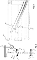
- Figure 4 illustrates a device in accordance with the present invention.
- a frame 45 comprises a lowering rail 47 across which a stepper motor 48 may lower the probe 1 towards the sample surface 9 of a sample 8.
- the probe 1 consists of the actuator stage implemented in its suspension structure 5, the cantilever 4 and a probe tip 3.
- the Z dimension is illustrated schematically with double arrow 50.
- Frame 45 further comprises a laser unit 55 that provides a laser beam 65 which impinges on the top 56 of the probe tip 3.
- a mirror or specular reflective surface is present on the probe tip 3, which reflects the reflector beam 65' towards an optical sensor system 58 that allows to determine the exact position at which the reflected beam 65' impinges on the sensor 58.
- the sensor signal is provided to a control unit 60 which also controls operation of the stepper motor 48.
- a voltage can be applied to the sample surface 9 of sample 8 by charging the carrier surface 53 which comprises electrodes underneath the sample 8.
- the scanning probe microscope comprises a power supply 67.
- the scanning probe microscope illustrated in figure 4 may apply any of the methods of the present invention either based on static deflection or on dynamic deflection, whichever embodiment of the present invention is considered most beneficial to the design of the system.
- Figure 5 illustrates a 3D graph of the electrostatic force as a function of the voltage applied and the distance to the surface, including a path taken in accordance with the controlled approach method of the present invention.
- the graph 75 is a three dimensional graph illustrating the distance r to the surface on axis 78, the applied voltage U on axis 79, and on axis 77 an approximation of the resulting force F including the electrostatic force and Van der Waals force exerted on the probe.
- a controlled approach method in accordance with an embodiment the present invention is schematically indicated by path 80.
- the controlled approach takes path 80 trough the r-U-F landscape in such a manner that the electrostatic force F is kept constant.
- the distance r to the surface is known. Adjusting the voltage effectively achieves adjustment of the electric field strength, and thereby enables to reduce the electrostatic force.
- the deflection can be kept static during the approach. This can be done stepwise or as a continuous process. The approach is complete upon reaching point 82 on path 80.
- inventive method has been described in terms of a number of method steps and optional method steps.
- the steps of the method may in accordance with some embodiments be performed simultaneously in a continuous manner. Alternatively, one or more steps may be performed sequentially, without departing from the inventive concept.
Landscapes
- Physics & Mathematics (AREA)
- Health & Medical Sciences (AREA)
- General Health & Medical Sciences (AREA)
- General Physics & Mathematics (AREA)
- Nuclear Medicine, Radiotherapy & Molecular Imaging (AREA)
- Radiology & Medical Imaging (AREA)
- Length Measuring Devices With Unspecified Measuring Means (AREA)
Claims (14)
- Verfahren zum Vorschieben einer Sondenspitze (3) einer Sonde (1) einer Rastermikroskopievorrichtung zu einer Probenoberfläche (9), wobei die Vorrichtung die Sonde (1) zum Abtasten der Probenoberfläche zum Abbilden von Nanostrukturen auf der Probenoberfläche (9) umfasst, wobei die Sondenspitze der Sonde an einem Ausleger (4) angebracht ist, der so angeordnet ist, dass er die Sondenspitze in Kontakt mit der Probenoberfläche bringt, wobei das Verfahren umfasst:Steuern eines Aktuatorsystems (5) der Vorrichtung zum Bewegen der Sonde zur Probenoberfläche durch eine Steuerung (60);Empfangen eines Sensorsignals durch die Steuerung (60), das wenigstens einen Betriebsparameter der Sonde angibt, um eine Rückmeldung zur Durchführung des Steuerns bereitzustellen;
wobei das Verfahren ferner umfasst:Aufrechterhalten eines elektrischen Feldes zwischen der Probenoberfläche (9) und der Sondenspitze (3) während des Steuerns, um eine elektrostatische Kraft auf die Sondenspitze auszuüben, die von der Nähe der Sondenspitze zur Oberfläche abhängt; undAuswerten des Sensorsignals, das den wenigstens einen Betriebsparameter angibt, um einen Einfluss des elektrischen Feldes auf die Sonde (1) zu bestimmen, um die Nähe der Probenoberfläche in Bezug auf die Sondenspitze (3) zu bestimmen; undwobei der Auswertungsschritt ferner das Vergleichen des Sensorsignals mit einem Referenzwert und das Steuern des Aktuatorsystems (5) in Abhängigkeit von dem Vergleich umfasst, wobei er ferner einen Schritt des Einstellens einer elektrischen Feldstärke des elektrischen Feldes in Abhängigkeit von dem Schritt des Auswertens umfasst, während die Sondenspitze (3) die Substratoberfläche (9) vorschiebt. - Verfahren nach Anspruch 1, wobei der Schritt des Aufrechterhaltens eines elektrischen Feldes das Aufrechterhalten einer Vorspannungsdifferenz V0 zwischen der Probenoberfläche (9) und der Sondenspitze (3) umfasst.
- Verfahren nach Anspruch 1 oder 2, wobei das Sensorsignal wenigstens eines aus einer Gruppe umfasst, die umfasst: ein Sondenspitzen-Auslenkungssignal, das eine Auslenkung w der Sondenspitze (3) aus einer Referenzposition ao angibt; Gütefaktor, Dämpfung, Phasenverzögerung, Phase, Krümmungsmessung, Interferenz, Piezowiderstand, Wellenlängenänderung eines in den Ausleger (4) integrierten Ringresonators oder Wellenleiters, kapazitive Änderungen.
- Verfahren nach einem der Ansprüche 2 und 3, wobei das Sensorsignal das Sondenspitzen-Auslenkungssignal umfasst, und wobei der Auswertungsschritt das Vergleichen der Auslenkung w der Sondenspitze (3) mit einer berechneten Auslenkung wc umfasst.
- Verfahren nach Anspruch 4, wobei die berechnete Auslenkung wc. durch Lösen und/oder Abschätzen einer Differentialgleichung erhalten wird:

- Verfahren nach einem der vorhergehenden Ansprüche, wobei der Schritt des Steuerns ferner umfasst:Steuern des Aktuatorsystems durch die Steuerung (60) während des Bewegens der Sonde, um eine Oszillatorbewegung auf die Sondenspitze auszuüben, so dass die Sondenspitze (3) in einer Richtung quer zur Probenoberfläche (9) oszilliert; undwobei das Sensorsignal wenigstens einen Parameter der Oszillatorbewegung angibt.
- Verfahren nach Anspruch 6, wobei das Sensorsignal wenigstens eines aus einer Gruppe umfasst, die umfasst: ein Sondenamplitudensignal, Gütefaktor, Dämpfung, Phasenverzögerung, Phase, Krümmungsmessung, Interferenz, Piezowiderstand, Wellenlängenänderung eines in den Ausleger (4) integrierten Ringresonators oder Wellenleiters, kapazitive Änderungen.
- Verfahren nach Anspruch 6 oder 7, wobei der Auswertungsschritt das Bestimmen des Parameters der oszillierenden Bewegung aus dem Sensorsignal und das Vergleichen des bestimmten Parameters mit einem Referenzwert zum Bestimmen einer Abweichung vom Referenzwert umfasst.
- Verfahren nach Anspruch 8, wobei das Verfahren das Reduzieren nach dem Bestimmen der Abweichung der Vorspannung (10) umfasst, so dass die Abweichung verringert wird, und dass die Schritte des Steuerns des Aktuatorsystems und des Empfangens und des Auswertens des Sensorsignals wiederholt werden.
- Verfahren nach Anspruch 9, wobei die Schritte des Reduzierens der Vorspannung (10), des Steuerns des Aktuatorsystems und des Empfangens und Auswertens des Sensorsignals wiederholt werden, bis die Vorspannung (10) auf Null reduziert ist.
- Verfahren zum Betreiben einer Rastermikroskopievorrichtung zum Abtasten der Probenoberfläche zum Abbilden der darauf befindlichen Nanostrukturen, wobei das Verfahren ein Verfahren zum Vorschieben einer Sondenspitze einer Sonde zu einer Probenoberfläche nach einem der vorhergehenden Ansprüche umfasst.
- Rastermikroskopievorrichtung zum Abbilden von Nanostrukturen auf einer Probenoberfläche (9) einer Probe (8), die wenigstens eine Sonde (1) zum Abtasten der Probenoberfläche (9) und ein Aktuatorsystem (5) zum Bewegen der Sonde zu und von der Probe (8), um sich der Probenoberfläche (9) anzunähern, umfasst, wobei die Sonde eine Sondenspitze (3) umfasst, die an einem Ausleger (4) angebracht ist, der so angeordnet ist, dass er die Sondenspitze in Kontakt mit der Probenoberfläche (9) bringt, um das Abtasten der Probenoberfläche zu ermöglichen, wobei die Vorrichtung ferner umfasst:eine Steuerung (60) zum Steuern des Aktuatorsystems (5) der Vorrichtung zum Bewegen der Sonde (1) zur Probenoberfläche (9), wobei die Steuerung (60) Eingabemittel umfasst, die kommunikativ mit einem Sensor (58) verbunden sind, um ein Sensorsignal zu empfangen, das wenigstens einen Betriebsparameter der Sonde angibt, um eine Rückmeldung zur Durchführung der Steuerung bereitzustellen; undeine oder mehrere Elektroden zum Aufbau und zum Aufrechterhalten eines elektrischen Feldes zwischen der Probenoberfläche (9) und der Sondenspitze (3), um eine elektrostatische Kraft auf die Sondenspitze auszuüben, die von der Nähe der Sondenspitze (3) zur Probenoberfläche (9) abhängig ist;wobei die Steuerung (60) ferner dazu eingerichtet ist, das Sensorsignal auszuwerten, das den wenigstens einen Betriebsparameter angibt, um einen Einfluss des elektrischen Feldes auf die Sonde (1) zu bestimmen, um die Nähe der Probenoberfläche (9) in Bezug auf die Sondenspitze (3) zu bestimmen;die Steuerung (60) zur Durchführung des Auswertens durch Vergleichen des Sensorsignals mit einem Referenzwert und zum Steuern des Aktuatorsystems (5) in Abhängigkeit von diesem Vergleich angeordnet ist; undwobei die Steuerung ferner zum Einstellen einer elektrischen Feldstärke des elektrischen Feldes in Abhängigkeit von dem Auswertungsschritt, während die Sondenspitze (3) die Substratoberfläche (9) vorschiebt, angeordnet ist.
- Rastermikroskopievorrichtung nach Anspruch 12, wobei das Aktuatorsystem ferner einen Oszillatortisch umfasst, und wobei die Steuerung (60) zum Steuern während das Bewegen der Sonde (1) in Richtung der Probenoberfläche (9) des Oszillatortisches des Aktuatorsystems (5), um eine Oszillatorbewegung auf die Sondenspitze auszuüben, so dass die Sondenspitze (3) in einer Richtung quer zur Probenoberfläche oszilliert, angeordnet ist und wobei der Sensor zum Bereitstellen eines Sensorsignals, das wenigstens einen Parameter der Oszillatorbewegung der Sonde angibt, angeordnet ist; und
wobei die Steuerung (60) zum Bestimmen des Parameters der oszillierenden Bewegung aus dem Sensorsignal und Vergleichen des bestimmten Parameters mit einem Referenzwert angeordnet ist, um eine Abweichung von dem Referenzwert zu bestimmen, und wobei die Steuerung (60) zum Reduzieren nach dem Bestimmen der Abweichung der Vorspannung (10) angeordnet ist, um die Abweichung zu verringern, und die Schritte des Steuerns des Aktuatorsystems (5) und des Empfangens und Auswertens des Sensorsignals zu wiederholen. - Computerprogrammprodukt, wobei das Computerprogrammprodukt, wenn es auf einer Rastermikroskopievorrichtung läuft, die wenigstens eine Sonde (1) zum Abtasten der Probenoberfläche (9) und ein Aktuatorsystem (5) zum Bewegen der Sonde (1) zu und von der Probe zum Annähern an die Probenoberfläche (9) umfasst, wobei die Sonde eine Sondenspitze (3) umfasst, die an einem Ausleger (4) angebracht ist, der so angeordnet ist, dass er die Sondenspitze (4) in Kontakt mit der Probenoberfläche (9) bringt, um das Abtasten der Probenoberfläche (9) zu ermöglichen, in der Lage ist, die Rastermikroskopievorrichtung zu betreiben, um die Sondenspitze (3) in Richtung der Probenoberfläche (9) gemäß einem Verfahren vorzuschieben, wie es in einem oder mehreren der Ansprüche 1 bis 11 definiert ist.
Applications Claiming Priority (2)
| Application Number | Priority Date | Filing Date | Title |
|---|---|---|---|
| EP14166220.5A EP2940480A1 (de) | 2014-04-28 | 2014-04-28 | Verfahren zum Vorschub einer Sondenspitze einer Rastermikroskopvorrichtung gegenüber einer Sondenoberfläche, und Vorrichtung dafür |
| PCT/NL2015/050281 WO2015167326A1 (en) | 2014-04-28 | 2015-04-28 | Method of advancing a probe tip of a scanning microscopy device towards a sample surface, and device therefore |
Publications (2)
| Publication Number | Publication Date |
|---|---|
| EP3137912A1 EP3137912A1 (de) | 2017-03-08 |
| EP3137912B1 true EP3137912B1 (de) | 2022-09-28 |
Family
ID=50555090
Family Applications (2)
| Application Number | Title | Priority Date | Filing Date |
|---|---|---|---|
| EP14166220.5A Withdrawn EP2940480A1 (de) | 2014-04-28 | 2014-04-28 | Verfahren zum Vorschub einer Sondenspitze einer Rastermikroskopvorrichtung gegenüber einer Sondenoberfläche, und Vorrichtung dafür |
| EP15724785.9A Active EP3137912B1 (de) | 2014-04-28 | 2015-04-28 | Verfahren zum vorschub einer sondenspitze einer rastermikroskopvorrichtung gegenüber einer sondenoberfläche, und vorrichtung dafür |
Family Applications Before (1)
| Application Number | Title | Priority Date | Filing Date |
|---|---|---|---|
| EP14166220.5A Withdrawn EP2940480A1 (de) | 2014-04-28 | 2014-04-28 | Verfahren zum Vorschub einer Sondenspitze einer Rastermikroskopvorrichtung gegenüber einer Sondenoberfläche, und Vorrichtung dafür |
Country Status (4)
| Country | Link |
|---|---|
| US (1) | US9766266B2 (de) |
| EP (2) | EP2940480A1 (de) |
| TW (1) | TWI666450B (de) |
| WO (1) | WO2015167326A1 (de) |
Families Citing this family (5)
| Publication number | Priority date | Publication date | Assignee | Title |
|---|---|---|---|---|
| US9891246B2 (en) * | 2015-08-06 | 2018-02-13 | Fardad Michael Serry | Harmonic feedback atomic force microscopy |
| EP3349018A1 (de) * | 2017-01-13 | 2018-07-18 | Nederlandse Organisatie voor toegepast- natuurwetenschappelijk onderzoek TNO | Atomkraftmikroskopievorrichtung, -verfahren und lithographiesystem |
| AT520313B1 (de) * | 2017-09-13 | 2019-03-15 | Anton Paar Gmbh | Handhabungsvorrichtung zum Handhaben einer Messsonde |
| GB201917596D0 (en) | 2019-12-02 | 2020-01-15 | Infinitesima Ltd | Scanning probe system |
| US12529724B2 (en) * | 2023-05-19 | 2026-01-20 | Fei Company | Capacitance-based detection of probe contact |
Family Cites Families (5)
| Publication number | Priority date | Publication date | Assignee | Title |
|---|---|---|---|---|
| US5874726A (en) * | 1995-10-10 | 1999-02-23 | Iowa State University Research Foundation | Probe-type near-field confocal having feedback for adjusting probe distance |
| US7473887B2 (en) * | 2002-07-04 | 2009-01-06 | University Of Bristol Of Senate House | Resonant scanning probe microscope |
| JP2006220599A (ja) * | 2005-02-14 | 2006-08-24 | Jeol Ltd | 走査形プローブ顕微鏡 |
| US7665349B2 (en) * | 2005-04-12 | 2010-02-23 | Veeco Instruments Inc. | Method and apparatus for rapid automatic engagement of a probe |
| JP4688643B2 (ja) * | 2005-11-10 | 2011-05-25 | エスアイアイ・ナノテクノロジー株式会社 | 加振型カンチレバーホルダ及び走査型プローブ顕微鏡 |
-
2014
- 2014-04-28 EP EP14166220.5A patent/EP2940480A1/de not_active Withdrawn
-
2015
- 2015-04-27 TW TW104113398A patent/TWI666450B/zh active
- 2015-04-28 US US15/306,742 patent/US9766266B2/en active Active
- 2015-04-28 EP EP15724785.9A patent/EP3137912B1/de active Active
- 2015-04-28 WO PCT/NL2015/050281 patent/WO2015167326A1/en not_active Ceased
Also Published As
| Publication number | Publication date |
|---|---|
| US20170052209A1 (en) | 2017-02-23 |
| EP3137912A1 (de) | 2017-03-08 |
| EP2940480A1 (de) | 2015-11-04 |
| TWI666450B (zh) | 2019-07-21 |
| TW201546456A (zh) | 2015-12-16 |
| WO2015167326A1 (en) | 2015-11-05 |
| US9766266B2 (en) | 2017-09-19 |
Similar Documents
| Publication | Publication Date | Title |
|---|---|---|
| Salapaka et al. | Scanning probe microscopy | |
| Abramovitch et al. | A tutorial on the mechanisms, dynamics, and control of atomic force microscopes | |
| Howland et al. | A practical guide: To scanning probe microscopy | |
| Yong et al. | Video-rate Lissajous-scan atomic force microscopy | |
| EP3137912B1 (de) | Verfahren zum vorschub einer sondenspitze einer rastermikroskopvorrichtung gegenüber einer sondenoberfläche, und vorrichtung dafür | |
| US9291640B2 (en) | Method and apparatus of using peak force tapping mode to measure physical properties of a sample | |
| EP2507642B1 (de) | Verfahren und vorrichtung zur bedienung eines rastersondenmikroskops | |
| US6167753B1 (en) | Detecting fields with a single-pass, dual-amplitude-mode scanning force microscope | |
| US8220066B2 (en) | Vibration compensation in probe microscopy | |
| EP2864798B1 (de) | Verfahren und vorrichtung zur messung elektrischer eigenschaften unter verwendung eines afm im spitzenkraft-erfassungsmodus | |
| JPH10332713A (ja) | 走査顕微鏡のプローブとセグメント化圧電アクチュエータとのかみ合いの制御 | |
| Gao | Surface metrology for micro-and nanofabrication | |
| US5773824A (en) | Method for improving measurement accuracy using active lateral scanning control of a probe | |
| Ito et al. | Development of a probing system for a micro-coordinate measuring machine by utilizing shear-force detection | |
| Wang et al. | Improving the scanning speed of atomic force microscopy at the scanning range of several tens of micrometers | |
| Xia et al. | Active Probe Atomic Force Microscopy | |
| Serry et al. | Characterization and Measurement of Microcomponents with the Atomic Force Microscope (AFM) | |
| US20150026846A1 (en) | Variable Density Scanning | |
| Chen et al. | Large-area profile measurement of sinusoidal freeform surfaces using a new prototype scanning tunneling microscopy | |
| Zhukov et al. | Scanning ion-conductance microscope with modulation of the sample position along the Z-coordinate and separate Z-axial and lateral (X, Y) scanning | |
| Gao et al. | A noncontact scanning electrostatic force microscope for surface profile measurement | |
| Saeidpourazar et al. | Microcantilever-based force tracking with applications to high-resolution imaging and nanomanipulation | |
| Haefliger et al. | An integrated piezo-acoustic shear-force distance sensor with nanometer resolution for a micropipette tool | |
| Gupta et al. | Design and application of a data driven controller using the small-gain constraint for positioning control of a nano-positioner | |
| Cui et al. | A high-speed atomic force microscope for precision measurement of microstructured surfaces |
Legal Events
| Date | Code | Title | Description |
|---|---|---|---|
| STAA | Information on the status of an ep patent application or granted ep patent |
Free format text: STATUS: THE INTERNATIONAL PUBLICATION HAS BEEN MADE |
|
| PUAI | Public reference made under article 153(3) epc to a published international application that has entered the european phase |
Free format text: ORIGINAL CODE: 0009012 |
|
| STAA | Information on the status of an ep patent application or granted ep patent |
Free format text: STATUS: REQUEST FOR EXAMINATION WAS MADE |
|
| 17P | Request for examination filed |
Effective date: 20161107 |
|
| AK | Designated contracting states |
Kind code of ref document: A1 Designated state(s): AL AT BE BG CH CY CZ DE DK EE ES FI FR GB GR HR HU IE IS IT LI LT LU LV MC MK MT NL NO PL PT RO RS SE SI SK SM TR |
|
| AX | Request for extension of the european patent |
Extension state: BA ME |
|
| DAV | Request for validation of the european patent (deleted) | ||
| DAX | Request for extension of the european patent (deleted) | ||
| STAA | Information on the status of an ep patent application or granted ep patent |
Free format text: STATUS: EXAMINATION IS IN PROGRESS |
|
| 17Q | First examination report despatched |
Effective date: 20190711 |
|
| GRAP | Despatch of communication of intention to grant a patent |
Free format text: ORIGINAL CODE: EPIDOSNIGR1 |
|
| STAA | Information on the status of an ep patent application or granted ep patent |
Free format text: STATUS: GRANT OF PATENT IS INTENDED |
|
| INTG | Intention to grant announced |
Effective date: 20220607 |
|
| GRAS | Grant fee paid |
Free format text: ORIGINAL CODE: EPIDOSNIGR3 |
|
| GRAA | (expected) grant |
Free format text: ORIGINAL CODE: 0009210 |
|
| STAA | Information on the status of an ep patent application or granted ep patent |
Free format text: STATUS: THE PATENT HAS BEEN GRANTED |
|
| AK | Designated contracting states |
Kind code of ref document: B1 Designated state(s): AL AT BE BG CH CY CZ DE DK EE ES FI FR GB GR HR HU IE IS IT LI LT LU LV MC MK MT NL NO PL PT RO RS SE SI SK SM TR |
|
| REG | Reference to a national code |
Ref country code: GB Ref legal event code: FG4D |
|
| REG | Reference to a national code |
Ref country code: CH Ref legal event code: EP |
|
| REG | Reference to a national code |
Ref country code: AT Ref legal event code: REF Ref document number: 1521567 Country of ref document: AT Kind code of ref document: T Effective date: 20221015 |
|
| REG | Reference to a national code |
Ref country code: DE Ref legal event code: R096 Ref document number: 602015080968 Country of ref document: DE |
|
| REG | Reference to a national code |
Ref country code: IE Ref legal event code: FG4D |
|
| REG | Reference to a national code |
Ref country code: NL Ref legal event code: FP |
|
| REG | Reference to a national code |
Ref country code: LT Ref legal event code: MG9D |
|
| PG25 | Lapsed in a contracting state [announced via postgrant information from national office to epo] |
Ref country code: SE Free format text: LAPSE BECAUSE OF FAILURE TO SUBMIT A TRANSLATION OF THE DESCRIPTION OR TO PAY THE FEE WITHIN THE PRESCRIBED TIME-LIMIT Effective date: 20220928 Ref country code: RS Free format text: LAPSE BECAUSE OF FAILURE TO SUBMIT A TRANSLATION OF THE DESCRIPTION OR TO PAY THE FEE WITHIN THE PRESCRIBED TIME-LIMIT Effective date: 20220928 Ref country code: NO Free format text: LAPSE BECAUSE OF FAILURE TO SUBMIT A TRANSLATION OF THE DESCRIPTION OR TO PAY THE FEE WITHIN THE PRESCRIBED TIME-LIMIT Effective date: 20221228 Ref country code: LV Free format text: LAPSE BECAUSE OF FAILURE TO SUBMIT A TRANSLATION OF THE DESCRIPTION OR TO PAY THE FEE WITHIN THE PRESCRIBED TIME-LIMIT Effective date: 20220928 Ref country code: LT Free format text: LAPSE BECAUSE OF FAILURE TO SUBMIT A TRANSLATION OF THE DESCRIPTION OR TO PAY THE FEE WITHIN THE PRESCRIBED TIME-LIMIT Effective date: 20220928 Ref country code: FI Free format text: LAPSE BECAUSE OF FAILURE TO SUBMIT A TRANSLATION OF THE DESCRIPTION OR TO PAY THE FEE WITHIN THE PRESCRIBED TIME-LIMIT Effective date: 20220928 |
|
| REG | Reference to a national code |
Ref country code: AT Ref legal event code: MK05 Ref document number: 1521567 Country of ref document: AT Kind code of ref document: T Effective date: 20220928 |
|
| PG25 | Lapsed in a contracting state [announced via postgrant information from national office to epo] |
Ref country code: HR Free format text: LAPSE BECAUSE OF FAILURE TO SUBMIT A TRANSLATION OF THE DESCRIPTION OR TO PAY THE FEE WITHIN THE PRESCRIBED TIME-LIMIT Effective date: 20220928 Ref country code: GR Free format text: LAPSE BECAUSE OF FAILURE TO SUBMIT A TRANSLATION OF THE DESCRIPTION OR TO PAY THE FEE WITHIN THE PRESCRIBED TIME-LIMIT Effective date: 20221229 |
|
| PG25 | Lapsed in a contracting state [announced via postgrant information from national office to epo] |
Ref country code: SM Free format text: LAPSE BECAUSE OF FAILURE TO SUBMIT A TRANSLATION OF THE DESCRIPTION OR TO PAY THE FEE WITHIN THE PRESCRIBED TIME-LIMIT Effective date: 20220928 Ref country code: RO Free format text: LAPSE BECAUSE OF FAILURE TO SUBMIT A TRANSLATION OF THE DESCRIPTION OR TO PAY THE FEE WITHIN THE PRESCRIBED TIME-LIMIT Effective date: 20220928 Ref country code: PT Free format text: LAPSE BECAUSE OF FAILURE TO SUBMIT A TRANSLATION OF THE DESCRIPTION OR TO PAY THE FEE WITHIN THE PRESCRIBED TIME-LIMIT Effective date: 20230130 Ref country code: ES Free format text: LAPSE BECAUSE OF FAILURE TO SUBMIT A TRANSLATION OF THE DESCRIPTION OR TO PAY THE FEE WITHIN THE PRESCRIBED TIME-LIMIT Effective date: 20220928 Ref country code: CZ Free format text: LAPSE BECAUSE OF FAILURE TO SUBMIT A TRANSLATION OF THE DESCRIPTION OR TO PAY THE FEE WITHIN THE PRESCRIBED TIME-LIMIT Effective date: 20220928 Ref country code: AT Free format text: LAPSE BECAUSE OF FAILURE TO SUBMIT A TRANSLATION OF THE DESCRIPTION OR TO PAY THE FEE WITHIN THE PRESCRIBED TIME-LIMIT Effective date: 20220928 |
|
| PG25 | Lapsed in a contracting state [announced via postgrant information from national office to epo] |
Ref country code: SK Free format text: LAPSE BECAUSE OF FAILURE TO SUBMIT A TRANSLATION OF THE DESCRIPTION OR TO PAY THE FEE WITHIN THE PRESCRIBED TIME-LIMIT Effective date: 20220928 Ref country code: PL Free format text: LAPSE BECAUSE OF FAILURE TO SUBMIT A TRANSLATION OF THE DESCRIPTION OR TO PAY THE FEE WITHIN THE PRESCRIBED TIME-LIMIT Effective date: 20220928 Ref country code: IS Free format text: LAPSE BECAUSE OF FAILURE TO SUBMIT A TRANSLATION OF THE DESCRIPTION OR TO PAY THE FEE WITHIN THE PRESCRIBED TIME-LIMIT Effective date: 20230128 Ref country code: EE Free format text: LAPSE BECAUSE OF FAILURE TO SUBMIT A TRANSLATION OF THE DESCRIPTION OR TO PAY THE FEE WITHIN THE PRESCRIBED TIME-LIMIT Effective date: 20220928 |
|
| P01 | Opt-out of the competence of the unified patent court (upc) registered |
Effective date: 20230522 |
|
| REG | Reference to a national code |
Ref country code: DE Ref legal event code: R097 Ref document number: 602015080968 Country of ref document: DE |
|
| PG25 | Lapsed in a contracting state [announced via postgrant information from national office to epo] |
Ref country code: AL Free format text: LAPSE BECAUSE OF FAILURE TO SUBMIT A TRANSLATION OF THE DESCRIPTION OR TO PAY THE FEE WITHIN THE PRESCRIBED TIME-LIMIT Effective date: 20220928 |
|
| PG25 | Lapsed in a contracting state [announced via postgrant information from national office to epo] |
Ref country code: DK Free format text: LAPSE BECAUSE OF FAILURE TO SUBMIT A TRANSLATION OF THE DESCRIPTION OR TO PAY THE FEE WITHIN THE PRESCRIBED TIME-LIMIT Effective date: 20220928 |
|
| PLBE | No opposition filed within time limit |
Free format text: ORIGINAL CODE: 0009261 |
|
| STAA | Information on the status of an ep patent application or granted ep patent |
Free format text: STATUS: NO OPPOSITION FILED WITHIN TIME LIMIT |
|
| 26N | No opposition filed |
Effective date: 20230629 |
|
| PG25 | Lapsed in a contracting state [announced via postgrant information from national office to epo] |
Ref country code: SI Free format text: LAPSE BECAUSE OF FAILURE TO SUBMIT A TRANSLATION OF THE DESCRIPTION OR TO PAY THE FEE WITHIN THE PRESCRIBED TIME-LIMIT Effective date: 20220928 |
|
| REG | Reference to a national code |
Ref country code: CH Ref legal event code: PL |
|
| GBPC | Gb: european patent ceased through non-payment of renewal fee |
Effective date: 20230428 |
|
| PG25 | Lapsed in a contracting state [announced via postgrant information from national office to epo] |
Ref country code: LU Free format text: LAPSE BECAUSE OF NON-PAYMENT OF DUE FEES Effective date: 20230428 |
|
| REG | Reference to a national code |
Ref country code: BE Ref legal event code: MM Effective date: 20230430 |
|
| PG25 | Lapsed in a contracting state [announced via postgrant information from national office to epo] |
Ref country code: MC Free format text: LAPSE BECAUSE OF FAILURE TO SUBMIT A TRANSLATION OF THE DESCRIPTION OR TO PAY THE FEE WITHIN THE PRESCRIBED TIME-LIMIT Effective date: 20220928 |
|
| PG25 | Lapsed in a contracting state [announced via postgrant information from national office to epo] |
Ref country code: GB Free format text: LAPSE BECAUSE OF NON-PAYMENT OF DUE FEES Effective date: 20230428 |
|
| PG25 | Lapsed in a contracting state [announced via postgrant information from national office to epo] |
Ref country code: MC Free format text: LAPSE BECAUSE OF FAILURE TO SUBMIT A TRANSLATION OF THE DESCRIPTION OR TO PAY THE FEE WITHIN THE PRESCRIBED TIME-LIMIT Effective date: 20220928 Ref country code: LI Free format text: LAPSE BECAUSE OF NON-PAYMENT OF DUE FEES Effective date: 20230430 Ref country code: GB Free format text: LAPSE BECAUSE OF NON-PAYMENT OF DUE FEES Effective date: 20230428 Ref country code: CH Free format text: LAPSE BECAUSE OF NON-PAYMENT OF DUE FEES Effective date: 20230430 |
|
| PG25 | Lapsed in a contracting state [announced via postgrant information from national office to epo] |
Ref country code: BE Free format text: LAPSE BECAUSE OF NON-PAYMENT OF DUE FEES Effective date: 20230430 |
|
| PG25 | Lapsed in a contracting state [announced via postgrant information from national office to epo] |
Ref country code: IT Free format text: LAPSE BECAUSE OF FAILURE TO SUBMIT A TRANSLATION OF THE DESCRIPTION OR TO PAY THE FEE WITHIN THE PRESCRIBED TIME-LIMIT Effective date: 20220928 |
|
| PG25 | Lapsed in a contracting state [announced via postgrant information from national office to epo] |
Ref country code: BG Free format text: LAPSE BECAUSE OF FAILURE TO SUBMIT A TRANSLATION OF THE DESCRIPTION OR TO PAY THE FEE WITHIN THE PRESCRIBED TIME-LIMIT Effective date: 20220928 |
|
| PG25 | Lapsed in a contracting state [announced via postgrant information from national office to epo] |
Ref country code: BG Free format text: LAPSE BECAUSE OF FAILURE TO SUBMIT A TRANSLATION OF THE DESCRIPTION OR TO PAY THE FEE WITHIN THE PRESCRIBED TIME-LIMIT Effective date: 20220928 |
|
| PGFP | Annual fee paid to national office [announced via postgrant information from national office to epo] |
Ref country code: NL Payment date: 20250418 Year of fee payment: 11 |
|
| PGFP | Annual fee paid to national office [announced via postgrant information from national office to epo] |
Ref country code: DE Payment date: 20250422 Year of fee payment: 11 |
|
| PGFP | Annual fee paid to national office [announced via postgrant information from national office to epo] |
Ref country code: FR Payment date: 20250425 Year of fee payment: 11 |
|
| PG25 | Lapsed in a contracting state [announced via postgrant information from national office to epo] |
Ref country code: CY Free format text: LAPSE BECAUSE OF FAILURE TO SUBMIT A TRANSLATION OF THE DESCRIPTION OR TO PAY THE FEE WITHIN THE PRESCRIBED TIME-LIMIT; INVALID AB INITIO Effective date: 20150428 |
|
| PGFP | Annual fee paid to national office [announced via postgrant information from national office to epo] |
Ref country code: IE Payment date: 20250422 Year of fee payment: 11 |
|
| PG25 | Lapsed in a contracting state [announced via postgrant information from national office to epo] |
Ref country code: HU Free format text: LAPSE BECAUSE OF FAILURE TO SUBMIT A TRANSLATION OF THE DESCRIPTION OR TO PAY THE FEE WITHIN THE PRESCRIBED TIME-LIMIT; INVALID AB INITIO Effective date: 20150428 |
|
| PG25 | Lapsed in a contracting state [announced via postgrant information from national office to epo] |
Ref country code: TR Free format text: LAPSE BECAUSE OF FAILURE TO SUBMIT A TRANSLATION OF THE DESCRIPTION OR TO PAY THE FEE WITHIN THE PRESCRIBED TIME-LIMIT Effective date: 20220928 |