EP3136608B1 - Method and system for providing low density parity check (ldpc) encoding and decoding - Google Patents
Method and system for providing low density parity check (ldpc) encoding and decoding Download PDFInfo
- Publication number
- EP3136608B1 EP3136608B1 EP16190032.9A EP16190032A EP3136608B1 EP 3136608 B1 EP3136608 B1 EP 3136608B1 EP 16190032 A EP16190032 A EP 16190032A EP 3136608 B1 EP3136608 B1 EP 3136608B1
- Authority
- EP
- European Patent Office
- Prior art keywords
- ldpc
- bit
- nodes
- check
- edge information
- Prior art date
- Legal status (The legal status is an assumption and is not a legal conclusion. Google has not performed a legal analysis and makes no representation as to the accuracy of the status listed.)
- Active
Links
- 238000000034 method Methods 0.000 title claims description 50
- 239000011159 matrix material Substances 0.000 claims description 46
- 238000004891 communication Methods 0.000 description 38
- 230000008569 process Effects 0.000 description 31
- 238000010586 diagram Methods 0.000 description 24
- 238000013459 approach Methods 0.000 description 21
- 238000012545 processing Methods 0.000 description 12
- 230000005540 biological transmission Effects 0.000 description 8
- 230000006870 function Effects 0.000 description 8
- 230000010363 phase shift Effects 0.000 description 8
- 230000003287 optical effect Effects 0.000 description 7
- 238000004088 simulation Methods 0.000 description 7
- 238000013461 design Methods 0.000 description 6
- 238000004904 shortening Methods 0.000 description 5
- 238000007792 addition Methods 0.000 description 3
- 230000008901 benefit Effects 0.000 description 3
- 230000001419 dependent effect Effects 0.000 description 3
- 125000004122 cyclic group Chemical group 0.000 description 2
- 230000007423 decrease Effects 0.000 description 2
- 230000033001 locomotion Effects 0.000 description 2
- 238000013507 mapping Methods 0.000 description 2
- 230000003068 static effect Effects 0.000 description 2
- RYGMFSIKBFXOCR-UHFFFAOYSA-N Copper Chemical compound [Cu] RYGMFSIKBFXOCR-UHFFFAOYSA-N 0.000 description 1
- 238000003491 array Methods 0.000 description 1
- 230000002238 attenuated effect Effects 0.000 description 1
- 230000015556 catabolic process Effects 0.000 description 1
- 230000001413 cellular effect Effects 0.000 description 1
- 238000010276 construction Methods 0.000 description 1
- 238000012937 correction Methods 0.000 description 1
- 230000008878 coupling Effects 0.000 description 1
- 238000010168 coupling process Methods 0.000 description 1
- 238000005859 coupling reaction Methods 0.000 description 1
- 238000006731 degradation reaction Methods 0.000 description 1
- 238000001514 detection method Methods 0.000 description 1
- 238000011161 development Methods 0.000 description 1
- 230000018109 developmental process Effects 0.000 description 1
- 230000008030 elimination Effects 0.000 description 1
- 238000003379 elimination reaction Methods 0.000 description 1
- 239000000835 fiber Substances 0.000 description 1
- 230000006872 improvement Effects 0.000 description 1
- 230000003993 interaction Effects 0.000 description 1
- 239000004973 liquid crystal related substance Substances 0.000 description 1
- 230000007246 mechanism Effects 0.000 description 1
- 238000012986 modification Methods 0.000 description 1
- 230000004048 modification Effects 0.000 description 1
- 230000008520 organization Effects 0.000 description 1
- 230000002093 peripheral effect Effects 0.000 description 1
- 230000009467 reduction Effects 0.000 description 1
- 230000001172 regenerating effect Effects 0.000 description 1
- 230000004044 response Effects 0.000 description 1
- 238000012546 transfer Methods 0.000 description 1
Images


Classifications
-
- H—ELECTRICITY
- H03—ELECTRONIC CIRCUITRY
- H03M—CODING; DECODING; CODE CONVERSION IN GENERAL
- H03M13/00—Coding, decoding or code conversion, for error detection or error correction; Coding theory basic assumptions; Coding bounds; Error probability evaluation methods; Channel models; Simulation or testing of codes
- H03M13/03—Error detection or forward error correction by redundancy in data representation, i.e. code words containing more digits than the source words
- H03M13/05—Error detection or forward error correction by redundancy in data representation, i.e. code words containing more digits than the source words using block codes, i.e. a predetermined number of check bits joined to a predetermined number of information bits
- H03M13/11—Error detection or forward error correction by redundancy in data representation, i.e. code words containing more digits than the source words using block codes, i.e. a predetermined number of check bits joined to a predetermined number of information bits using multiple parity bits
- H03M13/1102—Codes on graphs and decoding on graphs, e.g. low-density parity check [LDPC] codes
- H03M13/1148—Structural properties of the code parity-check or generator matrix
- H03M13/116—Quasi-cyclic LDPC [QC-LDPC] codes, i.e. the parity-check matrix being composed of permutation or circulant sub-matrices
- H03M13/1165—QC-LDPC codes as defined for the digital video broadcasting [DVB] specifications, e.g. DVB-Satellite [DVB-S2]
-
- H—ELECTRICITY
- H03—ELECTRONIC CIRCUITRY
- H03M—CODING; DECODING; CODE CONVERSION IN GENERAL
- H03M13/00—Coding, decoding or code conversion, for error detection or error correction; Coding theory basic assumptions; Coding bounds; Error probability evaluation methods; Channel models; Simulation or testing of codes
- H03M13/03—Error detection or forward error correction by redundancy in data representation, i.e. code words containing more digits than the source words
- H03M13/033—Theoretical methods to calculate these checking codes
- H03M13/036—Heuristic code construction methods, i.e. code construction or code search based on using trial-and-error
-
- H—ELECTRICITY
- H03—ELECTRONIC CIRCUITRY
- H03M—CODING; DECODING; CODE CONVERSION IN GENERAL
- H03M13/00—Coding, decoding or code conversion, for error detection or error correction; Coding theory basic assumptions; Coding bounds; Error probability evaluation methods; Channel models; Simulation or testing of codes
- H03M13/03—Error detection or forward error correction by redundancy in data representation, i.e. code words containing more digits than the source words
- H03M13/05—Error detection or forward error correction by redundancy in data representation, i.e. code words containing more digits than the source words using block codes, i.e. a predetermined number of check bits joined to a predetermined number of information bits
- H03M13/11—Error detection or forward error correction by redundancy in data representation, i.e. code words containing more digits than the source words using block codes, i.e. a predetermined number of check bits joined to a predetermined number of information bits using multiple parity bits
- H03M13/1102—Codes on graphs and decoding on graphs, e.g. low-density parity check [LDPC] codes
- H03M13/1105—Decoding
- H03M13/1111—Soft-decision decoding, e.g. by means of message passing or belief propagation algorithms
- H03M13/1117—Soft-decision decoding, e.g. by means of message passing or belief propagation algorithms using approximations for check node processing, e.g. an outgoing message is depending on the signs and the minimum over the magnitudes of all incoming messages according to the min-sum rule
- H03M13/1122—Soft-decision decoding, e.g. by means of message passing or belief propagation algorithms using approximations for check node processing, e.g. an outgoing message is depending on the signs and the minimum over the magnitudes of all incoming messages according to the min-sum rule storing only the first and second minimum values per check node
-
- H—ELECTRICITY
- H03—ELECTRONIC CIRCUITRY
- H03M—CODING; DECODING; CODE CONVERSION IN GENERAL
- H03M13/00—Coding, decoding or code conversion, for error detection or error correction; Coding theory basic assumptions; Coding bounds; Error probability evaluation methods; Channel models; Simulation or testing of codes
- H03M13/03—Error detection or forward error correction by redundancy in data representation, i.e. code words containing more digits than the source words
- H03M13/05—Error detection or forward error correction by redundancy in data representation, i.e. code words containing more digits than the source words using block codes, i.e. a predetermined number of check bits joined to a predetermined number of information bits
- H03M13/11—Error detection or forward error correction by redundancy in data representation, i.e. code words containing more digits than the source words using block codes, i.e. a predetermined number of check bits joined to a predetermined number of information bits using multiple parity bits
- H03M13/1102—Codes on graphs and decoding on graphs, e.g. low-density parity check [LDPC] codes
- H03M13/1105—Decoding
- H03M13/1131—Scheduling of bit node or check node processing
- H03M13/1137—Partly parallel processing, i.e. sub-blocks or sub-groups of nodes being processed in parallel
-
- H—ELECTRICITY
- H03—ELECTRONIC CIRCUITRY
- H03M—CODING; DECODING; CODE CONVERSION IN GENERAL
- H03M13/00—Coding, decoding or code conversion, for error detection or error correction; Coding theory basic assumptions; Coding bounds; Error probability evaluation methods; Channel models; Simulation or testing of codes
- H03M13/29—Coding, decoding or code conversion, for error detection or error correction; Coding theory basic assumptions; Coding bounds; Error probability evaluation methods; Channel models; Simulation or testing of codes combining two or more codes or code structures, e.g. product codes, generalised product codes, concatenated codes, inner and outer codes
- H03M13/2906—Coding, decoding or code conversion, for error detection or error correction; Coding theory basic assumptions; Coding bounds; Error probability evaluation methods; Channel models; Simulation or testing of codes combining two or more codes or code structures, e.g. product codes, generalised product codes, concatenated codes, inner and outer codes using block codes
-
- H—ELECTRICITY
- H03—ELECTRONIC CIRCUITRY
- H03M—CODING; DECODING; CODE CONVERSION IN GENERAL
- H03M13/00—Coding, decoding or code conversion, for error detection or error correction; Coding theory basic assumptions; Coding bounds; Error probability evaluation methods; Channel models; Simulation or testing of codes
- H03M13/03—Error detection or forward error correction by redundancy in data representation, i.e. code words containing more digits than the source words
- H03M13/05—Error detection or forward error correction by redundancy in data representation, i.e. code words containing more digits than the source words using block codes, i.e. a predetermined number of check bits joined to a predetermined number of information bits
- H03M13/13—Linear codes
- H03M13/15—Cyclic codes, i.e. cyclic shifts of codewords produce other codewords, e.g. codes defined by a generator polynomial, Bose-Chaudhuri-Hocquenghem [BCH] codes
- H03M13/151—Cyclic codes, i.e. cyclic shifts of codewords produce other codewords, e.g. codes defined by a generator polynomial, Bose-Chaudhuri-Hocquenghem [BCH] codes using error location or error correction polynomials
- H03M13/152—Bose-Chaudhuri-Hocquenghem [BCH] codes
Definitions
- Communication systems employ coding to ensure reliable communication across noisy communication channels. These communication channels exhibit a fixed capacity that can be expressed in terms of bits per symbol at certain signal to noise ratio (SNR), defining a theoretical upper limit (known as the Shannon limit). As a result, coding design has aimed to achieve rates approaching this Shannon limit.
- SNR signal to noise ratio
- coding design has aimed to achieve rates approaching this Shannon limit.
- One such class of codes that approach the Shannon limit is Low Density Parity Check (LDPC) codes.
- LDPC codes have not been widely deployed because of a number of drawbacks.
- One drawback is that the LDPC encoding technique is highly complex. Encoding an LDPC code using its generator matrix would require storing a very large, non-sparse matrix. Additionally, LDPC codes require large blocks to be effective; consequently, even though parity check matrices of LDPC codes are sparse, storing these matrices is problematic.
- LDPC codes have not become widespread in practice.
- a key challenge in LDPC code implementation has been how to achieve the connection network between several processing engines (nodes) in the decoder.
- the computational load in the decoding process specifically the check node operations, poses a problem.
- the decoding process involves iteratively regenerating signal constellation bit metrics into an LDPC decoder after each decoder iteration or several decoder iterations. This document is completely silent with respect to guaranteeing a convergence. This is a significant drawback.
- a method comprises accessing memory storing information representing a structured parity check matrix of Low Density Parity Check (LDPC) codes.
- the information is organized in tabular form, such each row represents occurrences of one value within a first column of a group of columns of the parity check matrix, the rows correspond to groups of columns of the parity check matrix. Also, subsequent columns within each of the groups are derived according to a predetermined operation. Further, an LDPC coded signal is outputted based on the stored information representing the parity check matrix.
- LDPC Low Density Parity Check
- an apparatus comprises a memory which is configured to store information representing a structured parity check matrix of Low Density Parity Check (LDPC) codes.
- the information is organized in tabular form, wherein each row represents occurrences of one values within a first column of a group of columns of the parity check matrix. Also, the rows correspond to groups of columns of the parity check matrix, where subsequent columns within each of the groups are derived according to a predetermined operation.
- the apparatus also comprises circuitry coupled to the memory and configured to output an LDPC coded signal using the stored information representing the parity check matrix.
- LDPC Low Density Parity Check
- a method comprises accessing memory storing edge information associated with a structured parity check matrix used to generate Low Density Parity Check (LDPC) coded signal.
- the edge information represent relationship between bit nodes and check nodes, and are stored according to a predetermined scheme that permits concurrent retrieval of a set of the edge information. Further, a decoded signal is outputted corresponding to the LDPC coded signal based on the stored edge information.
- LDPC Low Density Parity Check
- a method comprises accessing memory storing edge information and a posteriori probability information associated with a structured parity check matrix used to generate Low Density Parity Check (LDPC) coded signal.
- the edge information represents relationship between bit nodes and check nodes, and are stored according to a predetermined scheme that permits concurrent retrieval of a set of the edge information. Further, a decoded signal is outputted corresponding to the LDPC coded signal based on the stored edge and a posteriori probability information.
- LDPC Low Density Parity Check
- LDPC Low Density Parity Check
- FIG. 1 is a diagram of a communications system configured to utilize Low Density Parity Check (LDPC) codes, according to one embodiment.
- a digital communications system 100 includes a transmitter 101 that generates signal waveforms across a communication channel 103 to a receiver 105.
- the transmitter 101 has a message source that produces a discrete set of possible messages; each of the possible messages has a corresponding signal waveform. These signal waveforms are attenuated, or otherwise altered, by communications channel 103.
- LDPC codes are utilized.
- the LDPC codes that are generated by the transmitter 101 enable high speed implementation without incurring any performance loss.
- These structured LDPC codes output from the transmitter 101 avoid assignment of a small number of check nodes to the bit nodes already vulnerable to channel errors by virtue of the modulation scheme (e.g., quadrature phase-shift keying (QPSK), offset quadrature phase-shift keying (OQPSK), 8-PSK, 16 amplitude and phase-shift keying (16-APSK), etc.).
- the modulation scheme e.g., quadrature phase-shift keying (QPSK), offset quadrature phase-shift keying (OQPSK), 8-PSK, 16 amplitude and phase-shift keying (16-APSK), etc.
- Such LDPC codes have a parallelizable decoding algorithm (unlike turbo codes), which advantageously involves simple operations such as addition, comparison and table look-up. Moreover, carefully designed LDPC codes do not exhibit any sign of error floor.
- the transmitter 101 generates, using a relatively simple encoding technique, LDPC codes based on parity check matrices (which facilitate efficient memory access during decoding) to communicate with the receiver 105.
- the transmitter 101 employs LDPC codes that can outperform concatenated turbo+RS (Reed-Solomon) codes, provided the block length is sufficiently large.
- FIGs. 2A are diagrams of an exemplary LDPC encoders deployed in the transmitter of FIG. 1 , according to various exemplary embodiments.
- a transmitter 200 can be equipped with an LDPC encoder 203 that accepts input from an information source 201 and outputs coded stream of higher redundancy suitable for error correction processing at the receiver 105.
- the information source 201 can generate k signals from a discrete alphabet, X .
- LDPC codes can be specified with parity check matrices.
- encoding LDPC codes may require, in general, specifying the generator matrices. Even though it is possible to obtain generator matrices from parity check matrices using Gaussian elimination, the resulting matrix is no longer sparse and storing a large generator matrix can be complex.
- Encoder 203 generates signals from alphabet Y to a modulator 205 using a simple encoding technique that makes use of the parity check matrix by imposing structure onto the parity check matrix.
- a restriction can be placed on the parity check matrix by constraining certain portion of the matrix to be triangular. The construction of such a parity check matrix is described more fully below in FIG. 6 . Such a restriction can result in negligible performance loss, and therefore, constitutes an attractive trade-off.
- Modulator 205 maps the encoded messages from encoder 203 to signal waveforms that are transmitted to a transmit antenna 207, which emits these waveforms over the communication channel 103. Accordingly, the encoded messages are modulated and distributed to a transmit antenna 207.
- the modulation can include quadrature phase-shift keying (QPSK), offset quadrature phase-shift keying (OQPSK), 8-PSK, and/or 16 amplitude and phase-shift keying (16-APSK) modulation.
- QPSK quadrature phase-shift keying
- OFQPSK offset quadrature phase-shift keying
- 8-PSK 8-PSK
- 16-APSK 16 amplitude and phase-shift keying
- the transmission of the codeword starts in the given order from i 0 and ends with p n ldpc - k ldpc -1.
- LDPC codes three different code rates can be defined: 1/2, 2/3, and 4/5.
- 22 different coded block sizes can be defined: 720, 960, 1200, 1440, 1680, 1920, 2160, 2400, 2640, 2880, 3120, 3360, 3600, 3840, 4080, 4320, 4560, 4800, 5040, 5280, 5520, and 5760 coded bits, corresponding to 3 up to 24 slots.
- bursts longer than 24 slots can be obtained by coding multiple shorter LDPC codes of "almost equal" sizes.
- mother LDPC codes which include 720, 960, 1440, 2160, 2880, 3600, 4320, and 5760 bit blocks.
- the other 14 codes can be derived from the mother codes by shortening and puncturing, as discussed below.
- shortening and puncturing process can be explained with respect to FIG. 2C .
- XS bits starting from index XS start in the input block are set to 0 before encoding (per step 221). After encoding, these bits are omitted from the resulting codeword before transmission (per steps 223 and 225).
- the following XP parity bits are not transmitted p 0, pXP period , p 2 XP period ,... p ( XP -1) XP period , where XP period is a code dependent parameter (per step 227).
- K mother and N mother denote the number of un-coded and coded bits of the mother code, respectively
- K mother ⁇ XS , N N mother ⁇ XS ⁇ XP .
- K and N denote the number of un-coded and coded bits of the derived code, respectively.
- the degree distribution of bit nodes is given in Table 2 below, where N denotes the total number of bit nodes, i.e., coded block size.
- N denotes the total number of bit nodes, i.e., coded block size.
- the remaining check node has degree one less.
- the task of the LDPC encoder 203 is to determine n ldpc k ldpc parity bits ( p 0 ,..., pn ldpc -k ldpc -1) for every block of k ldpc information bits, ( i 0 , i 1 ,..., i kldpc -1).
- the addresses of the parity bit accumulators are given in the second row of the Tables 3 through 26.
- a new row from Tables 3 through 26 are used to find the addresses of the parity bit accumulators.
- FIG. 2B shows an LDPC encoder utilized with a Bose Chaudhuri Hocquenghem (BCH) encoder 209 and an interleaver 211, according to another exemplary embodiment.
- the codes generated by the LDPS encoder 203 and the BCH 209 can have a concatenated outer BCH code.
- the output of the LDPC encoder can be bit interleaved using the interleaver 211.
- the interleaver 211 can be a block interleaver.
- the interleaver 211 can be an optional element in the transmitter and instead an interleaver in a receiver (such as receiver 105) can be used to interleave decoder input.
- a cyclic redundancy check (CRC) encoder (not shown) can be connected to the BCH encoder 209 such that error detection can be achieved using cyclic redundancy check (CRC) codes.
- CRC cyclic redundancy check
- the transmission of the codeword starts in the given order from i 0 and ends with pn ldpc -k ldpc -1.
- another set of LDPC codes can be defined.
- the LDPC code parameters ( n ldpc , k ldpc ), according to these exemplary embodiments, are given in Table 27 below.
- Table 27 LDPC Code Parameters ( n ldpc ,k ldpc ) Code Rate LDPC Uncoded Block Length k ldpc LDPC Coded Block Length n ldpc 1/4 16200 64800 1/3 21600 64800 2/5 25920 64800 1/2 32400 64800 3/5 38880 64800 2/3 43200 64800 3/4 48600 64800 4/5 51840 64800 5/6 54000 64800 8/9 57600 64800 9/10 58320 64800
- the addresses of the parity bit accumulators are given in the second row of the Tables 28 through 38.
- a new row from Tables 28 through 38 are used to find the addresses of the parity bit accumulators.
- the generator polynomial of the t error correcting BCH encoder 209 is obtained by multiplying the first t polynomials in the following list of Table 39: Table 39 g 1 (x) 1+x 2 +x 3 +x 5 +x 16 g 2 (x) 1+x+x 4 +x 5 +x 6 +x 8 +x 16 g 3 (x) 1+x 2 +x 3 +x 4 +x 5 +x 7 +x 8 +x 9 +x 10 +x 11 +x 16 g 4 (x) 1+x 2 +x 4 +x 6 +x 9 +x 11 +x 12 +x 14 +x 16 g 5 (x) 1+x+x 2 +x 3 +x 5 +x 8 +x 9 +x 10 +x 11 +x 12 +x 16 g 6 (x) 1+x 2 +x 4 +x 5 +x 7 +x 8 +x 9 +x 10 +x 12 +x 13 +x 14 +x 15 +x 16 g 7 (x) 1+x 2 +x 5 +x 6 +x 8 x+
- m ( x ) m kbch -1 x k bch -1 + m k bch -2 x k bch -2 +...+ m 1 x + m 0 is multiplied by x n bch -k bch .
- x n bch -k bch m ( x ) is divided by g(x).
- the output of the LDPC encoder 203 can be bit interleaved using the interleaver 211.
- the interleaving process can be performed for 8-PSK and/or 16-APSP modulations.
- Data can be serially written into the interleaver 211 column-wise (from the top to the bottom), and can be serially read out row-wise (from the left to the right except for the rate 3/5 8-PSK case where data is read out from the right to the left).
- the configuration of the interleaver 211 for each modulation format can be viewed in Table 40.
- FIG. 2D is a flowchart of the LDPC encoding process as discussed above, according to an exemplary embodiment.
- the information bits are received and LDPC codes are generated at step 233.
- the structure of the LDPC codes (stemming from the design of the parity check matrix) permits an efficient decoding process, whereby parallel computation engines can be utilized.
- the LDPC code can be generated with out BCH codes and codes also can contain a CRC code.
- the coded bits are altered by the interleaver 211, as described above.
- the codes are modulated per step 237 and are transmitted on the communication channel.
- the above LDPC codes in an exemplary embodiment, can be used to variety of digital video applications, such as MPEG (Motion Pictures Expert Group) packet transmission.
- MPEG Motion Pictures Expert Group
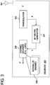
- FIG. 3 is a diagram of a receiver configured to operate in the system of FIG. 1 , according to an exemplary embodiment.
- a receiver 300 includes an antenna 301 that receives the waveforms emitted over the channel 103.
- the receiver provides a demodulator 303 that performs demodulation of the received signals from, for instance, transmitter 200.
- the received signals are forwarded to a decoder 305, which attempts to reconstruct the original source messages by generating messages, X' , in conjunction with a bit metric generator 307.
- the decoder 305 can employ M parallel engines 309 to efficiently decode the received signals.
- M may correspond to the groupings of M bit nodes for processing; this parallel approach is more fully described later.
- the demodulator 303 in accordance with the bit metric generator 307 can provide a priori probabilities of log likelihood ratios of coded bits.
- the above transmitter 200 and receiver 300 can be deployed within a single wireless terminal, in which case a common antenna system can be shared.
- the wireless terminal can for example be configured to operate within a satellite communication, a cellular system, wireless local area network (WLAN), etc.
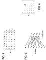
- FIG. 4 is a diagram of a sparse parity check matrix, in accordance with an exemplary embodiment.
- LDPC codes are long, linear block codes with sparse parity check matrix H ( n-k ) xn .
- the block length, n ranges from thousands to tens of thousands of bits.
- the same code can be equivalently represented by the bipartite graph, per FIG. 5 .
- FIG. 5 is a diagram of a bipartite graph of an LDPC code of the matrix of FIG. 4 .
- Parity check equations imply that for each check node, the sum (over GF (Galois Field)(2)) of all adjacent bit nodes is equal to zero.
- the LDPC decoder 305 is considered a message passing decoder, whereby the decoder 305 aims to find the values of bit nodes. To accomplish this task, bit nodes and check nodes iteratively communicate with each other. The nature of this communication is described below.
- each bit node From bit nodes to check nodes, each bit node relays to an adjacent check node an estimate about its own value based on the feedback coming from its other adjacent check nodes.
- n 1 has only two adjacent check nodes m 1 and m 3 . If the feedback coming from m 3 to n 1 indicates that the value of n 1 is probably 0, then n 1 would notify m 1 that an estimate of n 1 's own value is 0.
- the bit node performs a majority vote (soft decision) on the feedback coming from its other adjacent check nodes before reporting that decision to the check node it communicates. The above process is repeated until all bit nodes are considered to be correct (i.e., all parity check equations are satisfied) or until a predetermined maximum number of iterations is reached, whereby a decoding failure is declared.
- FIG. 6 is a diagram of a sub-matrix of a sparse parity check matrix, wherein the sub-matrix contains parity check values restricted to the lower triangular region, according to an exemplary embodiment.
- the encoder 203 (of FIG. 2 ) can employ a simple encoding technique by restricting the values of the lower triangular area of the parity check matrix.
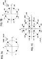
- FIGs. 7A-7C illustrate, respectively, diagrams of QPSK, 8-PSK, and 16-APSK modulation schemes, which can be used in the system of FIG. 1 , according to various exemplary embodiments.
- the QPSK modulation scheme of FIG. 7A can be used.
- the I/Q demodulated output of demodulator 303 of receiver 305 can be first multiplied by a constant and then quantized to a nearest integer between a predetermined range, e.g., -15 and +15.
- a predetermined range e.g., -15 and +15.
- the noise-free QPSK symbol is on the unit circle.
- the QPSK, 8-PSK, and 16-APSK modulation schemes of FIGs.7A-7C can be used for LDPC codes with code rates 1/4, 1/3, 2/5, 1/2, 3/5, 2/3, 3/4, 4/5, 5/6, 8/9, and 9/10 with coded block size 64800.
- bits 3 i +2, 3 i +1, 3 i of the output of the interleaver 211 of FIG. 2B determine the i th 8-PSK symbol.
- a decoding process in accordance with Gray mapping can be used.
- outgoing messages from bit nodes are initialized, check nodes are updated, bit nodes are updated, a posteriori probability information is outputted, a determination is made whether all parity check equations are satisfied, and a hard decision is outputted. Otherwise, check node update, bit node update, and outputting a posteriori probability information is repeated.
- a decoding process in accordance with non-Gray mapping can used such that probability information can be exchanged back and forth (iteratively) between the decoder 305 and bit metric generator 307 (of FIG. 3 ) during the decoding process.
- bit metrics and channel input are re-derived, bit node is updated, and the decoding process repeats with updating the check nodes.
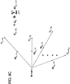
- FIG. 8A is a flowchart of a process for computing outgoing messages between the check nodes and the bit nodes using a forward-backward approach, according to an exemplary embodiment.
- the process 800 of FIG. 8A is explained with reference to diagrams of FIGs. 9A-9C .
- check nodes can be updated based on incoming messages (that, for example, can be performed in accordance with FIG. 9B ).
- the forward-backward approach can reduce the complexity of the computation to almost 3d c (for example, 3( d c -2)), in which d c -1 variables are stored.
- the incoming messages to the check node k from d c adjacent bit nodes are denoted by v n 1 ⁇ k , v n 2 ⁇ k , ...,v n dc ⁇ k . It is desired that the outgoing messages are computed from the check node k back to d c adjacent bit nodes; these outgoing messages are denoted by w k ⁇ n 1 , w k ⁇ n 2 ,..., w k ⁇ n dc .
- these forward variables are computed (which can be performed in almost d c clock cycle), and stored, per step 803.
- these backward variables are then computed (which can be performed in almost d c clock cycles). Thereafter, the outgoing messages are computed, as in step 807, based on the stored forward variables and the computed backward variables.
- the computation load can be further enhanced by using an enhanced layered belief decoding (LBD) approach, as discussed next.
- LBD enhanced layered belief decoding
- use of the LBD approach can enhance the decoding technique by improving convergence of about half the standard belief decoding (SBD) iterations, therefore, increasing the speed of decoding by almost 2.
- improvements discussed below with respect to FIG. 8B can further increase the speed of LBD approach by another factor of almost 2.5 by simplifying the g (.,.) function.
- FIG. 8B is a flowchart of process for computing outgoing messages between the check nodes and the bit nodes using an enhanced layered belief decoding (LBD) approach, according to an exemplary embodiment.
- LBD enhanced layered belief decoding
- FIG. 8B a simplified g (.,.) function is computed which decreases the clock cycle of the forward-backward approach of FIG. 8A from almost 3d c clock cycles to d c clock cycles.
- the incoming messages to the check node k from d c adjacent bit nodes are denoted by v n 1 ⁇ k , v n 2 ⁇ k ,..., v n dc ⁇ k . It is desired that the outgoing messages are computed from the check node k back to d c adjacent bit nodes; these outgoing messages are denoted by w k ⁇ n 1 , w k ⁇ n 2 ,..., w k ⁇ n dc .
- v n p ⁇ k min v n 1 ⁇ k , v n 2 ⁇ k , ... , v n dc ⁇ k
- the outgoing messages are computed, as in step 817, based on the determined variables, according to one exemplary embodiment.
- the computation of the outgoing messages can be performed in d c clock cycles.
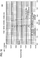
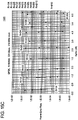
- FIG. 10 is a graph illustrating simulation results for the LBD scheme without simplified g (.,.) function, with simplified g (.,.) function with enhancement, and with g (.,.) function without enhancement, according to an exemplary embodiment.
- the simulations are performed for a LDPC code with code rate of 5/6, with 16-APSK, and with coded block size of 64800. It is noted that performance of the LBD scheme without simplification and the LBD scheme with simplification and with enhancements are close, although the speed of the LBD scheme with simplification and with enhancements is almost 2.5 times higher than the LBD scheme without simplification. Further, FIG. 10 illustrates that how the enhancements in the simplification of the g (.,.) function can improve the overall performance of the enhanced LBD scheme.
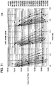
- FIG. 11 is a graph showing simulation results of LDPC codes for code rates 1/2, 2/3, and 4/5 for coded block sizes 720, 960, 1200, 1440, 1680, 1920, 2160, 2400, 2640, 2880, 3120, 3360, 3600, 3840, 4080, 4320, 4560, 4800, 5040, 5280, 5520, and 5760 coded bits generated in accordance with various exemplary embodiments.
- FIG. 11 shows the performance of fixed-point LDPC codes with 50 decoder iterations.
- the fully parallel architecture may involve greater complexity in realizing all of the nodes and their connections. Therefore with fully parallel architecture, a smaller block size may be required to reduce the complexity. In that case, for the same clock frequency, a proportional reduction in throughput and some degradation in FER versus Es/No performance may result.
- the second approach to implementing LDPC codes is to physically realize only a subset of the total number of the nodes and use only these limited number of "physical" nodes to process all of the "functional" nodes of the code. Even though the LDPC decoder operations can be made extremely simple and can be performed in parallel, the further challenge in the design is how the communication is established between "randomly" distributed bit nodes and check nodes.
- the decoder 305 (of FIG. 3 ), according to one embodiment, addresses this problem by accessing memory in a structured way, as to realize a seemingly random code. This approach is explained with respect to FIGs. 12A and 12B .
- FIGs. 12A and 12B are diagrams of the top edge and bottom edge, respectively, of memory organized to support structured access as to realize randomness in LDPC coding, according to an exemplary embodiment.
- Structured access can be achieved without compromising the performance of a truly random code by focusing on the generation of the parity check matrix.
- a parity check matrix can be specified by the connections of the check nodes with the bit nodes.
- the bit nodes can be divided into groups of a fixed size, which for illustrative purposes is M.
- M is number of parallel computation engines.
- the check nodes connected to the first bit node are different from a, b, c so that with a suitable choice of p, all the check nodes have the same degree.
- a random search can be performed over the free constants such that the resulting LDPC code is cycle-4 and cycle-6 free.
- the edge information can be stored to permit concurrent access to a group of relevant edge values during decoding.
- the approach facilitates memory access during check node and bit node processing.
- the values of the edges in the bipartite graph can be stored in a storage medium, such as random access memory (RAM). It is noted that for a truly random LDPC code during check node and bit node processing, the values of the edges would need to be accessed one by one in a random fashion. However, such a conventional access scheme would be too slow for a high data rate application.
- the RAM of FIGs. 12A and 12B are organized in a manner, whereby a large group of relevant edges can be fetched in one clock cycle; accordingly, these values are placed "together" in memory, according to a predetermined scheme or arrangement.
- each box contains the value of an edge, which is multiple bits (e.g., 6 bits).
- Edge RAM according to an exemplary embodiment, is conceptually divided into two parts, top edge RAM 1201 ( FIG. 12A ) and bottom edge RAM 1203 ( FIG. 12B ).
- Bottom edge RAM 1303 contains the edges between bit nodes of degree 2, for instance, (or 1 for one single bit node) and check nodes.
- Top edge RAM 1201 contains the edges between bit nodes of degree greater than 2 and check nodes. Therefore, according to an exemplary embodiment, for every check node, 2 adjacent edges are stored in the bottom RAM 1203, and the rest of the edges are stored in the top edge RAM 1201.
- a group of M bit nodes and M check nodes is processed at a time.
- q d c -2 consecutive rows from top edge RAM 1201 and 2 consecutive rows from bottom edge RAM 1203 is accessed, which the value of d c can depend on the code rate.
- d c 7 , 11, and 20 for rates 1/2, 2/3, and 4/5, respectively.
- bit node processing if the group of M bit nodes are parity bit nodes, their edges are located in 2 consecutive rows of the bottom edge RAM 1303. If the bit nodes are information bit nodes with degree d v >2, their edges are located in some d v rows of the top edge RAM 1201. The address of these d v rows can be stored in non-volatile memory, such as Read-Only Memory (ROM).
- ROM Read-Only Memory
- the edges in one of the rows correspond to the first edges of M bit nodes, the edges in another row correspond to the second edges of M bit nodes, etc.
- the column index of the edge that belongs to the first bit node in the group of M can also be stored in ROM. The edges that correspond to the second, third, etc.
- bit nodes follow the starting column index in a "wrapped around" fashion. For example, if the j th edge in the row belongs to the first bit node, then the ( j +1)st edge belongs to the second bit node, ( j +2)nd edge belongs to the third bit node, ...., and ( j -1)st edge belongs to the M th bit node.
- FIGs. 13A-13D are diagrams of parity check matrix, bipartite graph, top edge RAM, and bottom edge RAM, respectively, to support structured access as to realize randomness in LDPC coding, according to an exemplary embodiment.
- FIG. 13A illustrates a sparse parity check matrix 1301 of an LDPC code, according to an exemplary embodiment and FIG. 13B illustrates the corresponding bipartite graph 1303 of the LDPC code of the matrix 1301.
- the arrangement of top edge RAM 1305 is illustrated in FIG. 13C and the arrangement of bottom edge RAM 1307 is illustrated in FIG. 13D .
- d c -2 6 adjacent edges are e 0 e 1 e 2 e 3 e 4 e 5 , e 12 e 13 e 14 e 15 e 16 e 17 , e 24 e 25 e 26 e 27 e 28 e 29 . All the above edges are stored in the first 6 rows of top edge RAM 1305. Therefore, it is only needed that those 6 rows be fetched.
- the j th element belongs to the j th check node in the group.
- the remaining adjacent edges are e 36 e 39 e 40 e 43 e 44 . These remaining edges are stored in the first two rows of bottom edge RAM 1307. Similar to top edge RAM 1305 case, in each row, the j th element belongs to the j th check node in the group. Similar structure exists for the other group of check nodes. Therefore, as far as check node processing is concerned, there is no need for any ROM storage. Simply, consecutive rows of edge RAM's are accessed and within each row, it is known exactly where to find the edge for a particular check node in the group.
- Bit nodes in the first group have degree 3 and their adjacent edges are e 0 e 14 e 19 , e 12 e 26 e 31 , e 2 e 7 e 24 . All these edges can appear in top edge RAM 1305, namely rows indexed 0, 2 and 7. These row indices can be stored in ROM.
- Row 0 carries e 0 e 12 e 24 ; row 2 carries e 2 e 14 e 26 ; and row 7 carries e 7 e 19 e 31 .
- each row carries one adjacent edge per bit node.
- the j th element in each row does not necessarily belong to the j th node.
- ( j +1) st element belongs to the second bit
- ( j +2) nd element belongs to the third bit node. etc.
- ( j -1) st element belongs to the M th bit node (in a barrel shifted manner). Therefore, all needed to be stored in ROM is the index j of each row that belongs to the first bit node in the group.
- the I/Q demodulation output can be multiplied by a constant (quantized to the nearest integer between -15 and +15), and can be further fed to the LDCP decoder.
- check nodes can have degree d More specifically all the check nodes in the code bipartite graph (as illustrated in, for instance, FIG. 9B ) have degree d (i.e., they have d adjacent edges) except the first check node which has degree d -1 .
- N-K d -1 edges exist. These edges are denoted by e 1 , e 2 , e 3 ,...., e d- 1 ,e d +1 ,...,e ( N-K ) d .
- e 1 ,e 2 ,e 3 ,...., e d- 1 denote the edges adjacent to the first check node
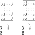
- FIGs. 14A-14C are diagrams of the edge, a posteriori, and shifted a posteriori, respectively, of memory organized to support LDPC decoding, according to an exemplary embodiment.
- the decoding process based on FIGs. 14A-14C is performed in accordance with LDPC codes with code rates 1/4, 1/3, 2/5, 1/2, 3/5, 2/3, 3/4, 4/5, 5/6, 8/9, and 9/10 with coded block size 64800.
- code rates 1/4, 1/3, 2/5, 1/2, 3/5, 2/3, 3/4, 4/5, 5/6, 8/9, and 9/10 with coded block size 64800 are examples of code rates 1/4, 1/3, 2/5, 1/2, 3/5, 2/3, 3/4, 4/5, 5/6, 8/9, and 9/10 with coded block size 64800.
- code rates and block sizes can be used.
- the edge values and a posteriori probability values can be arranged in the edge storage medium (such as random access memory (RAM)) 1401 of FIG. 14A and a posteriori storage medium (such as random access memory (RAM)) 1403 of FIG. 14B , respectively.
- edge storage medium such as random access memory (RAM)
- RAM random access memory
- RAM random access memory
- the first d rows of edge RAM 1401 can carry the edges adjacent to the first group of M check nodes. Further, the next d rows of the edge RAM 1401 can carry the edges adjacent to the second group of M check nodes, etc. Moreover in each row of the edge RAM 1401, the element in the i th column carries the edge adjacent to the i th check node in a group of M check nodes. It is noted that there is no edge value for the entry x in the edge RAM 1401. In one example, 9 bits can be allocated for the edge RAM 1401. Also, the edge RAM 1401 can be initialized with all zero entries.
- a posteriori RAM 1403 includes a posteriori probability values and in one example, 10 bits are allocated for the entries a posteriori RAM 1403.
- the a posteriori RAM 1403 can, initially be filled with LDPC decoder soft inputs, which, for instance, can be 6 bits. As the iterations of the decoder, for instance, decoder 303, are run, new a posteriori probability values for each coded bit overwrites the pervious value in the a posteriori RAM 1403.
- the LDPC decoder can process M check nodes in parallel.
- M 360.
- the decoder reads the first d rows of the edge RAM 1401 and a certain set of d rows from the a posteriori RAM 1403.
- the entries are circularly shifted to the left a certain number of times before they are aligned by the contents of the edge RAM 1401.
- FIG. 14C illustrates a shifted a posteriori RAM 1405 with the elements of the d circularly shifted rows, according to an exemplary embodiment.
- the output message from the i th check node is also computed as follows: z ⁇ min ⁇
- ⁇ , let z
- FIGs. 15A-15C are graphs showing simulation results of LDPC codes generated in accordance with various exemplary embodiments.
- FIGs. 15A-15C illustrate the performance of LDPC codes with QPSK, 8-PSK, and 16-APSK for different code rates.
- LDPC Low Density Parity Check
- FIG. 16 illustrates computing hardware (e.g., computer system) 1600 upon which an embodiment according to the invention can be implemented.
- the computer system 1600 includes a bus 1601 or other communication mechanism for communicating information and one or more processors (of which one is shown) 1603 coupled to the bus 1601 for processing information.
- the computer system 1600 also includes main memory 1605, such as a random access memory (RAM) or other dynamic storage device, coupled to the bus 1601 for storing information and instructions to be executed by the processor 1603.
- Main memory 1605 can also be used for storing temporary variables or other intermediate information during execution of instructions by the processor 1603.
- the computer system 1600 may further include a read only memory (ROM) 1607 or other static storage device coupled to the bus 1601 for storing static information and instructions for the processor 1603.
- a storage device 1609 such as a magnetic disk or optical disk, is coupled to the bus 1601 for persistently storing information and instructions.
- the computer system 1600 may be coupled via the bus 1601 to a display 1611, such as a cathode ray tube (CRT), liquid crystal display, active matrix display, or plasma display, for displaying information to a computer user.
- a display 1611 such as a cathode ray tube (CRT), liquid crystal display, active matrix display, or plasma display
- An input device 1613 such as a keyboard including alphanumeric and other keys, is coupled to the bus 1601 for communicating information and command selections to the processor 1603.
- a cursor control 1615 such as a mouse, a trackball, or cursor direction keys, for communicating direction information and command selections to the processor 1603 and for adjusting cursor movement on the display 1611.
- the processes described herein are performed by the computer system 1600, in response to the processor 1603 executing an arrangement of instructions contained in main memory 1605.
- Such instructions can be read into main memory 1605 from another computer-readable medium, such as the storage device 1609.
- Execution of the arrangement of instructions contained in main memory 1605 causes the processor 1603 to perform the process steps described herein.
- processors in a multi-processing arrangement may also be employed to execute the instructions contained in main memory 1605.
- hard-wired circuitry may be used in place of or in combination with software instructions to implement the embodiment of the invention.
- embodiments of the invention are not limited to any specific combination of hardware circuitry and software.
- the computer system 1600 also includes a communication interface 1617 coupled to bus 1601.
- the communication interface 1617 provides a two-way data communication coupling to a network link 1619 connected to a local network 1621.
- the communication interface 1617 may be a digital subscriber line (DSL) card or modem, an integrated services digital network (ISDN) card, a cable modem, a telephone modem, or any other communication interface to provide a data communication connection to a corresponding type of communication line.
- communication interface 1617 may be a local area network (LAN) card (e.g. for EthernetTM or an Asynchronous Transfer Model (ATM) network) to provide a data communication connection to a compatible LAN.
- LAN local area network
- Wireless links can also be implemented.
- communication interface 1617 sends and receives electrical, electromagnetic, or optical signals that carry digital data streams representing various types of information.
- the communication interface 1617 can include peripheral interface devices, such as a Universal Serial Bus (USB) interface, a PCMCIA (Personal Computer Memory Card International Association) interface, etc.
- USB Universal Serial Bus
- PCMCIA Personal Computer Memory Card International Association
- the network link 1619 typically provides data communication through one or more networks to other data devices.
- the network link 1619 may provide a connection through local network 1621 to a host computer 1623, which has connectivity to a network 1625 (e.g. a wide area network (WAN) or the global packet data communication network now commonly referred to as the "Internet") or to data equipment operated by a service provider.
- the local network 1621 and the network 1625 both use electrical, electromagnetic, or optical signals to convey information and instructions.
- the signals through the various networks and the signals on the network link 1619 and through the communication interface 1617, which communicate digital data with the computer system 1600, are exemplary forms of carrier waves bearing the information and instructions.
- the computer system 1600 can send messages and receive data, including program code, through the network(s), the network link 1619, and the communication interface 1617.
- a server (not shown) might transmit requested code belonging to an application program for implementing an embodiment of the invention through the network 1625, the local network 1621 and the communication interface 1617.
- the processor 1603 may execute the transmitted code while being received and/or store the code in the storage device 1609, or other non-volatile storage for later execution. In this manner, the computer system 1600 may obtain application code in the form of a carrier wave.
- Non-volatile media include, for example, optical or magnetic disks, such as the storage device 1609.
- Volatile media include dynamic memory, such as main memory 1605.
- Transmission media include coaxial cables, copper wire and fiber optics, including the wires that comprise the bus 1601. Transmission media can also take the form of acoustic, optical, or electromagnetic waves, such as those generated during radio frequency (RF) and infrared (IR) data communications.
- RF radio frequency
- IR infrared
- Computer-readable media include, for example, a floppy disk, a flexible disk, hard disk, magnetic tape, any other magnetic medium, a CD-ROM, CDRW, DVD, any other optical medium, punch cards, paper tape, optical mark sheets, any other physical medium with patterns of holes or other optically recognizable indicia, a RAM, a PROM, and EPROM, a FLASH-EPROM, any other memory chip or cartridge, a carrier wave, or any other medium from which a computer can read.
- a floppy disk a flexible disk, hard disk, magnetic tape, any other magnetic medium, a CD-ROM, CDRW, DVD, any other optical medium, punch cards, paper tape, optical mark sheets, any other physical medium with patterns of holes or other optically recognizable indicia, a RAM, a PROM, and EPROM, a FLASH-EPROM, any other memory chip or cartridge, a carrier wave, or any other medium from which a computer can read.
- the instructions for carrying out at least part of the embodiments of the invention may initially be borne on a magnetic disk of a remote computer.
- the remote computer loads the instructions into main memory and sends the instructions over a telephone line using a modem.
- a modem of a local computer system receives the data on the telephone line and uses an infrared transmitter to convert the data to an infrared signal and transmit the infrared signal to a portable computing device, such as a personal digital assistant (PDA) or a laptop.
- PDA personal digital assistant
- An infrared detector on the portable computing device receives the information and instructions borne by the infrared signal and places the data on a bus.
- the bus conveys the data to main memory, from which a processor retrieves and executes the instructions.
- the instructions received by main memory can optionally be stored on storage device either before or after execution by processor.
Description
- Communication systems employ coding to ensure reliable communication across noisy communication channels. These communication channels exhibit a fixed capacity that can be expressed in terms of bits per symbol at certain signal to noise ratio (SNR), defining a theoretical upper limit (known as the Shannon limit). As a result, coding design has aimed to achieve rates approaching this Shannon limit. One such class of codes that approach the Shannon limit is Low Density Parity Check (LDPC) codes.
- Traditionally, LDPC codes have not been widely deployed because of a number of drawbacks. One drawback is that the LDPC encoding technique is highly complex. Encoding an LDPC code using its generator matrix would require storing a very large, non-sparse matrix. Additionally, LDPC codes require large blocks to be effective; consequently, even though parity check matrices of LDPC codes are sparse, storing these matrices is problematic.
- From an implementation perspective, a number of challenges are confronted. For example, storage is an important reason why LDPC codes have not become widespread in practice. Also, a key challenge in LDPC code implementation has been how to achieve the connection network between several processing engines (nodes) in the decoder. Further, the computational load in the decoding process, specifically the check node operations, poses a problem.
- Therefore, there is a need for an LDPC communication system that employs simple encoding and decoding processes. There is also a need for using LDPC codes efficiently to support high data rates, without introducing greater complexity. There is also a need to improve performance of LDPC encoders and decoders. There is also a need to minimize storage requirements for implementing LDPC coding. There is a further need for a scheme that simplifies the communication between processing nodes in the LDPC decoder.
- The document Mustafa Eroz et al.: "Structured low-density parity-check code design for next generation digital video broadcast", Military Communication Conference, 2005, MILCON 2005, IEEE, Atlantic City, NJ, USA, 17 October, 2005, pages 1 - 6 describes LDPC decoding using parallel decoder engines. However, the decoding procedure in this document only also includes hard decision decoding. Soft decision decoding using additionally a posteriori probability values in a LDPC decoder organized as turbo decoder and processed in parallel decoder engines can also not be found in this document.
- According to
US 2004/0005865 A1 , the decoding process involves iteratively regenerating signal constellation bit metrics into an LDPC decoder after each decoder iteration or several decoder iterations. This document is completely silent with respect to guaranteeing a convergence. This is a significant drawback. - From said drawback, it can be deduced that the object for a person skilled in the art is to develop a method for a soft decision LDPC decoding with guaranteed convergence.
- This object is solved by the features of claim 1. The other claims contain further developments of the invention.
- These and other needs are addressed by the present invention, wherein various approaches for encoding and decoding structured Low Density Parity Check (LDPC) codes is provided.
- According to one aspect of an exemplary embodiment, a method comprises accessing memory storing information representing a structured parity check matrix of Low Density Parity Check (LDPC) codes. The information is organized in tabular form, such each row represents occurrences of one value within a first column of a group of columns of the parity check matrix, the rows correspond to groups of columns of the parity check matrix. Also, subsequent columns within each of the groups are derived according to a predetermined operation. Further, an LDPC coded signal is outputted based on the stored information representing the parity check matrix. Parity bit accumulators are to initialized to zero, and first information bit in the j th group of M information bits is accumulated in the i th parity bit accumulator if the i th entry in (jM)th column of the parity check matrix is 1, where j=0,1,2,3,...k ldpc/M-1, the remaining (M-1) information bits m=jM+1, jM+2, jM+3,..., (j+1)M-1 of the j th group being accumulated in the parity bit accumulators according to {x+m mod M×q}mod(nldpc-kldpc ), wherein x denotes the address of the parity bit accumulator corresponding to the first bit, jM, in the group, and

- According to another aspect of an exemplary embodiment, an apparatus comprises a memory which is configured to store information representing a structured parity check matrix of Low Density Parity Check (LDPC) codes. The information is organized in tabular form, wherein each row represents occurrences of one values within a first column of a group of columns of the parity check matrix. Also, the rows correspond to groups of columns of the parity check matrix, where subsequent columns within each of the groups are derived according to a predetermined operation. The apparatus also comprises circuitry coupled to the memory and configured to output an LDPC coded signal using the stored information representing the parity check matrix. Parity bit accumulators are to initialized to zero, and first information bit in the j th group of M information bits is accumulated in the i th parity bit accumulator if the i th entry in (jM)th column of the parity check matrix is 1, where j=0,1,2,3,...k ldpc/M-1, the remaining (M-1) information bits m=jM+1, jM+2, jM+3,..., (j+1)M-1 of the j th group being accumulated in the parity bit accumulators according to {x + m mod M×q}mod(nldpc-kldpc ), wherein x denotes the address of the parity bit accumulator corresponding to the first bit, jM, in the group, and

- According to another aspect of an exemplary embodiment, a method comprises accessing memory storing edge information associated with a structured parity check matrix used to generate Low Density Parity Check (LDPC) coded signal. The edge information represent relationship between bit nodes and check nodes, and are stored according to a predetermined scheme that permits concurrent retrieval of a set of the edge information. Further, a decoded signal is outputted corresponding to the LDPC coded signal based on the stored edge information.
- According to another aspect of an exemplary embodiment, a method comprises accessing memory storing edge information and a posteriori probability information associated with a structured parity check matrix used to generate Low Density Parity Check (LDPC) coded signal. The edge information represents relationship between bit nodes and check nodes, and are stored according to a predetermined scheme that permits concurrent retrieval of a set of the edge information. Further, a decoded signal is outputted corresponding to the LDPC coded signal based on the stored edge and a posteriori probability information.
- Still other aspects, features, and advantages of the present invention are readily apparent from the following detailed description, simply by illustrating a number of particular embodiments and implementations, including the best mode contemplated for carrying out the present invention. The present invention is defined by the features of claim 1. Accordingly, the drawing and description are to be regarded as illustrative in nature, and not as restrictive.
- The present invention is illustrated by way of example, and not by way of limitation, in the figures of the accompanying drawings and in which like reference numerals refer to similar elements and in which:
-
FIG. 1 is a diagram of a communications system configured to utilize Low Density Parity Check (LDPC) codes, according to an exemplary embodiment; -
FIGs. 2A-2D are diagrams of exemplary LDPC encoders deployed in the transmitter ofFIG. 1 and exemplary encoding processes, according to various exemplary embodiments; -
FIG. 3 is a diagram of an exemplary receiver in the system ofFIG. 1 , according to an exemplary embodiment; -
FIG. 4 is a diagram of a sparse parity check matrix, according to an exemplary embodiment; -
FIG. 5 is a diagram of a bipartite graph of an LDPC code of the matrix ofFIG. 4 , according to an exemplary embodiment; -
FIG. 6 is a diagram of a sub-matrix of a sparse parity check matrix, wherein the sub-matrix contains parity check values restricted to the lower triangular region, according to an exemplary embodiment; -
FIGs. 7A-7C are, respectively, a diagram of a quadrature phase-shift keying (QPSK), an 8-PSK, and a 16 amplitude and phase-shift keying (16-APSK) modulation scheme, respectively, each of which can be used in the system ofFIG. 1 , according to an exemplary embodiment; -
FIGs. 8A and 8B are flowcharts of processes for computing outgoing messages between the check nodes and the bit nodes using, respectively, a forward-backward approach and an enhanced layered belief decoding (LBD) scheme, according to various exemplary embodiments; -
FIGs. 9A-9C are diagrams of the interactions between the check nodes and the bit nodes in a decoding process, according to an exemplary embodiment; -
FIG. 10 is a graph illustrating simulation results for the enhanced LBD scheme, according to an exemplary embodiment; -
FIG. 11 is a graph showing simulation results of LDPC codes generated in accordance with various exemplary embodiments; -
FIGs. 12A and12B are diagrams of the top edge and bottom edge, respectively, of memory organized to support structured access as to realize randomness in LDPC coding, according to an exemplary embodiment; -
FIGs. 13A-13D are diagrams of parity check matrix, bipartite graph, top edge RAM, and bottom edge RAM, respectively, to support structured access as to realize randomness in LDPC coding/decoding, according to an exemplary embodiment; -
FIGs. 14A-14C are diagrams of the edge, a posteriori, and shifted a posteriori, respectively, of memory organized to support LDPC decoding, according to an exemplary embodiment. -
FIGs. 15A-15C are graphs showing simulation results of LDPC codes generated in accordance with various exemplary embodiments; and -
FIG. 16 is a diagram of a computer system that can perform the processes of encoding and decoding of LDPC codes, in accordance with embodiments of the present invention. - A system, method, and software for efficiently encoding and decoding structured Low Density Parity Check (LDPC) codes are described. In the following description, for the purposes of explanation, numerous specific details are set forth in order to provide a thorough understanding of the present invention. In other instances, well-known structures and devices are shown in block diagram form in order to avoid unnecessarily obscuring the present invention.
-
FIG. 1 is a diagram of a communications system configured to utilize Low Density Parity Check (LDPC) codes, according to one embodiment. A digital communications system 100 includes a transmitter 101 that generates signal waveforms across a communication channel 103 to a receiver 105. In this discrete communications system 100, the transmitter 101 has a message source that produces a discrete set of possible messages; each of the possible messages has a corresponding signal waveform. These signal waveforms are attenuated, or otherwise altered, by communications channel 103. To combat the noise channel 103, LDPC codes are utilized. - The LDPC codes that are generated by the transmitter 101 enable high speed implementation without incurring any performance loss. These structured LDPC codes output from the transmitter 101 avoid assignment of a small number of check nodes to the bit nodes already vulnerable to channel errors by virtue of the modulation scheme (e.g., quadrature phase-shift keying (QPSK), offset quadrature phase-shift keying (OQPSK), 8-PSK, 16 amplitude and phase-shift keying (16-APSK), etc.).
- Such LDPC codes have a parallelizable decoding algorithm (unlike turbo codes), which advantageously involves simple operations such as addition, comparison and table look-up. Moreover, carefully designed LDPC codes do not exhibit any sign of error floor.
- According to one embodiment, the transmitter 101 generates, using a relatively simple encoding technique, LDPC codes based on parity check matrices (which facilitate efficient memory access during decoding) to communicate with the receiver 105. The transmitter 101 employs LDPC codes that can outperform concatenated turbo+RS (Reed-Solomon) codes, provided the block length is sufficiently large.
-
FIGs. 2A are diagrams of an exemplary LDPC encoders deployed in the transmitter ofFIG. 1 , according to various exemplary embodiments. As illustrated inFIG. 2A , a transmitter 200 can be equipped with an LDPC encoder 203 that accepts input from an information source 201 and outputs coded stream of higher redundancy suitable for error correction processing at the receiver 105. The information source 201 can generate k signals from a discrete alphabet, X. LDPC codes can be specified with parity check matrices. On the other hand, encoding LDPC codes may require, in general, specifying the generator matrices. Even though it is possible to obtain generator matrices from parity check matrices using Gaussian elimination, the resulting matrix is no longer sparse and storing a large generator matrix can be complex. - Encoder 203 generates signals from alphabet Y to a modulator 205 using a simple encoding technique that makes use of the parity check matrix by imposing structure onto the parity check matrix. According to certain embodiments, a restriction can be placed on the parity check matrix by constraining certain portion of the matrix to be triangular. The construction of such a parity check matrix is described more fully below in
FIG. 6 . Such a restriction can result in negligible performance loss, and therefore, constitutes an attractive trade-off. - Modulator 205 maps the encoded messages from encoder 203 to signal waveforms that are transmitted to a transmit antenna 207, which emits these waveforms over the communication channel 103. Accordingly, the encoded messages are modulated and distributed to a transmit antenna 207. In an exemplary embodiment, the modulation can include quadrature phase-shift keying (QPSK), offset quadrature phase-shift keying (OQPSK), 8-PSK, and/or 16 amplitude and phase-shift keying (16-APSK) modulation. The transmissions from the transmit antenna 207 propagate to a receiver, as discussed below.
- The LDPC encoder 203 systematically encodes an information block of size kldpc , i = (i 0, i 1,...,ik
ldpc -1) onto a codeword of size nldpc , c = (i 0, i 1,..., ikldpc -1, p 0, p 1,...pnldpc -kldpc -1). The transmission of the codeword starts in the given order from i 0 and ends with pnldpc -kldpc -1. - According to certain embodiments, for LDPC codes three different code rates can be defined: 1/2, 2/3, and 4/5. Also, for each code rate 1/2, 2/3, and 4/5, 22 different coded block sizes can be defined: 720, 960, 1200, 1440, 1680, 1920, 2160, 2400, 2640, 2880, 3120, 3360, 3600, 3840, 4080, 4320, 4560, 4800, 5040, 5280, 5520, and 5760 coded bits, corresponding to 3 up to 24 slots. Further, bursts longer than 24 slots can be obtained by coding multiple shorter LDPC codes of "almost equal" sizes. Among these 22 block sizes, eight of them correspond to mother LDPC codes, which include 720, 960, 1440, 2160, 2880, 3600, 4320, and 5760 bit blocks. The other 14 codes can be derived from the mother codes by shortening and puncturing, as discussed below.
- According to an exemplary embodiment, shortening and puncturing process can be explained with respect to
FIG. 2C . In on example, for the shortening process, XS bits starting from index XSstart in the input block are set to 0 before encoding (per step 221). After encoding, these bits are omitted from the resulting codeword before transmission (per steps 223 and 225). Additionally or alternatively, for the puncturing process, the following XP parity bits are not transmitted p0,pXPperiod , p2XPperiod ,...p(XP-1)XPperiod , where XPperiod is a code dependent parameter (per step 227). - For each block size which is not a mother code size, the parameters related to shortening and puncturing as well as the mother codes are given in Table 1 below. Note that if Kmother and Nmother denote the number of un-coded and coded bits of the mother code, respectively, for the derived code:

Table 1 Parameters Related to Shortening and Puncturing Rate/Block Size XS XSstart XP XP period Mother Code 1/2 1200 120 0 120 6 1/2 1440 1/2 1680 240 0 240 4 1/2 2160 1/2 1920 120 0 120 9 1/2 2160 1/2 2400 240 0 240 4 1/2 2880 1/2 2640 120 0 120 12 1/2 2880 1/2 3120 240 0 240 7 1/2 3600 1/2 3360 120 0 120 15 1/2 3600 1/2 3840 240 0 240 9 1/2 4320 1/2 4080 120 0 120 18 1/2 4320 1/2 4560 600 0 600 3 1/2 5760 1/2 4800 480 0 480 3 1/2 5760 1/2 5040 360 0 360 8 1/2 5760 1/2 5280 240 0 240 12 1/2 5760 1/2 5520 120 0 120 24 1/2 5760 2/3 1200 160 480 80 6 2/3 1440 2/3 1680 320 720 160 3 2/3 2160 2/3 1920 160 720 80 9 2/3 2160 2/3 2400 320 960 160 6 2/3 2880 2/3 2640 160 960 80 12 2/3 2880 2/3 3120 320 1200 160 7 2/3 3600 2/3 3360 160 1200 80 15 2/3 3600 2/3 3840 320 1440 160 9 2/3 4320 2/3 4080 160 1440 80 18 2/3 4320 2/3 4560 800 1920 400 3 2/3 5760 2/3 4800 640 1920 320 3 2/3 5760 2/3 5040 480 1920 240 8 2/3 5760 2/3 5280 320 1920 160 7 2/3 5760 2/3 5520 160 1920 80 24 2/3 5760 4/5 1200 192 288 48 6 4/5 1440 4/5 1680 384 1104 96 4 4/5 2160 4/5 1920 192 432 48 9 4/5 2160 4/5 2400 384 576 96 6 4/5 2880 4/5 2640 192 576 48 12 4/5 2880 4/5 3120 384 720 96 7 4/5 3600 4/5 3360 192 720 48 15 4/5 3600 4/5 3840 384 864 96 9 4/5 4320 4/5 4080 192 864 48 18 4/5 4320 4/5 4560 960 1152 240 4 4/5 5760 4/5 4800 768 1152 192 6 4/5 5760 4/5 5040 576 1152 144 8 4/5 5760 4/5 5280 384 1152 96 12 4/5 5760 4/5 5520 192 1152 48 24 4/5 5760 - In this exemplary embodiment, for each mother LDPC code, the degree distribution of bit nodes is given in Table 2 below, where N denotes the total number of bit nodes, i.e., coded block size. For each code, all of the check nodes except one have the same degree, namely dc =7 for rate 1/2, dc =11 for rate 2/3, and dc =20 for rate 4/5. The remaining check node has degree one less.
Degree Distribution of Bit Nodes Rate 8 7 6 5 4 3 2 1 Table 2 1/2 N/4 N/4 N/2-1 1 2/3 N/6 N/6 N/3 N/3-1 1 4/5 2N/5 2N/5 N/5-1 1 - According to certain embodiments, the task of the LDPC encoder 203 is to determine nldpc kldpc parity bits (p 0,...,pnldpc-kldpc -1) for every block of kldpc information bits, (i 0,i 1,...,ikldpc -1). In one exemplary embodiment, for instance when LDPC codes with code rates 1/2, 2/3, and 4/5 for coded block sizes 720, 960, 1200, 1440, 1680, 1920, 2160, 2400, 2640, 2880, 3120, 3360, 3600, 3840, 4080, 4320, 4560, 4800, 5040, 5280, 5520, and 5760 coded bits are to be generated, the procedure can be as follows. First, the parity bits are initialized; p0 = p 1 = p 2 = ... = pnldpc -kldpc -1= 0. The first information bit, i 0, is accumulated at parity bit addresses specified in the first row of Tables 3 through 26. For example, for rate 2/3 and code block 720 (Table 3), the following results:

- Then, for the next M-1 information bits, im , m = 1,2, ...,M-1, these bits are accumulated at parity bit addresses {x + m modM × q}mod(nldpc - kldpc ), where x denotes the address of the parity bit accumulator corresponding to the first bit i 0, M is number of columns in edge RAM (Table 44), and


- For the (M+1)st information bit iM , the addresses of the parity bit accumulators are given in the second row of the Tables 3 through 26. In a similar manner the addresses of the parity bit accumulators for the following M-1 information bits im,m = M + 1,M +2,...,2M-1 are obtained using the formula {x + m mod M×q}mod(nldpc -kldpc ), where x denotes the address of the parity bit accumulator corresponding to the information bit iM , i.e., the entries in the second row of the Tables 3 - 26. In a similar manner, for every group of M new information bits, a new row from Tables 3 through 26 are used to find the addresses of the parity bit accumulators.
- After all of the information bits are exhausted, the final parity bits are obtained as follows. First, the following operations are performed, starting with i = 1

Table 3 Address of Parity Bit Accumulators (Rate 2/3 - Coded Block Size 720) 83 117 156 169 231 126 112 106 120 169 106 27 188 213 22 159 160 121 106 203 196 141 174 135 64 137 226 91 180 85 166 7 82 7 198 148 134 24 9 83 149 160 1 151 74 203 116 13 206 12 101 200 45 98 16 235 165 167 25 171 2 83 33 8 174 207 36 170 207 73 172 86 Table 4 Address of Parity Bit Accumulators (Rate 2/3 - Coded Block Size 960) 52 293 211 106 128 87 286 89 224 273 74 99 28 301 142 311 160 201 210 123 252 165 198 183 296 105 10 283 244 317 302 263 289 168 207 267 167 170 141 156 270 266 240 171 89 28 237 158 113 67 118 66 160 22 144 269 180 53 59 121 36 183 238 171 140 314 271 168 42 153 173 31 Table 5 Address of Parity Bit Accumulators (Rate 2/3 -Coded Block Size 1440) 140 296 319 355 373 182 329 266 144 169 426 155 348 381 78 87 120 169 242 371 292 13 286 95 280 449 10 371 396 405 78 15 317 42 380 336 254 233 301 60 251 175 218 120 465 147 390 407 387 273 287 120 279 97 404 22 283 323 256 453 182 77 449 90 20 48 466 415 301 474 228 350 Table 6 Address of Parity Bit Accumulators (Rate 2/3 - Coded Block Size 2160) 458 368 73 243 357 298 305 695 375 511 575 629 186 130 624 561 297 284 204 637 10 623 195 436 300 433 110 712 401 618 379 608 710 700 390 535 73 478 524 641 456 554 363 400 174 463 249 575 228 542 556 493 30 684 581 225 195 134 61 82 461 45 387 244 91 128 71 246 439 212 274 359 476 394 234 171 501 391 327 528 41 186 62 253 513 295 157 661 152 196 16 490 710 239 257 96 687 710 408 525 160 18 671 331 370 101 68 695 Table 7 Address of Parity Bit Accumulators (Rate 2/3 - Coded Block Size 2880) 689 581 139 306 45 371 886 576 864 596 6 651 693 810 770 281 270 557 325 275 561 672 196 22 620 324 77 312 851 642 917 480 375 88 57 746 364 910 527 644 753 823 360 921 218 411 908 190 327 111 217 269 888 307 914 934 785 439 682 171 60 686 959 308 79 103 568 563 337 312 523 352 906 492 471 800 250 867 303 860 287 619 702 706 262 430 9 941 293 225 244 626 629 918 697 381 145 371 102 597 575 280 464 618 388 509 844 631 525 123 362 611 638 271 26 433 548 485 745 726 561 742 125 754 318 457 864 219 632 354 688 116 523 425 552 935 147 735 956 807 610 421 60 142 Table 8 Address of Parity Bit Accumulators (Rate 2/3 - Coded Block Size 3600) 157 563 346 756 65 524 238 859 133 475 1007 791 420 858 76 301 284 200 701 389 119 1155 823 1078 812 853 194 459 500 415 346 448 381 418 343 1048 452 724 87 169 402 105 410 511 534 417 676 883 762 170 553 957 559 618 276 41 2 505 486 607 308 389 110 251 1052 834 570 871 69 1124 923 1102 760 445 906 167 68 792 573 254 684 999 752 981 442 651 372 1113 366 204 230 25 1 160 426 171 768 909 61 798 10 369 60 174 167 59 915 728 356 655 456 997 967 37 755 113 1045 142 443 934 297 930 1156 502 597 452 760 439 725 889 1093 1100 48 377 511 752 330 817 1155 239 1006 823 522 725 95 871 813 30 92 539 1164 504 545 707 141 714 38 923 874 369 623 904 541 340 756 382 273 661 1195 194 29 931 1008 1178 687 326 18 927 246 488 976 Table 9 Address of Parity Bit Accumulators (Rate 2/3 - Coded Block Size 4320) 1029 1059 593 574 702 1161 695 1357 1081 1333 648 1179 898 1266 88 924 914 633 5 924 1123 291 191 48 113 1434 11 1094 102 337 695 504 348 286 209 712 85 207 748 1340 653 203 1365 377 983 1436 1308 962 1228 319 680 1114 1070 39 307 45 1375 416 1095 982 917 1281 912 434 355 165 527 513 36 655 86 530 313 556 630 1112 1306 851 904 666 44 487 166 565 335 521 699 272 1177 1228 1301 630 10 59 326 639 601 1326 1065 1142 107 1124 1074 1374 469 1262 508 867 525 588 827 209 1105 123 1383 1037 960 992 129 1397 1075 810 1015 1167 244 427 1272 786 44 560 88 787 362 565 688 1365 1066 622 1192 674 727 802 1100 1342 296 801 120 1147 453 1019 800 1332 1139 776 478 1249 1002 1252 862 91 178 1375 375 385 682 1095 51 285 744 187 1343 178 371 415 1119 1325 1332 688 873 494 295 1150 1182 122 733 137 572 981 589 672 1242 914 534 417 277 1288 1070 68 268 1202 884 461 1295 642 335 1384 926 1433 821 27 97 1156 732 1299 1278 593 Table 10 Address of Parity Bit Accumulators (Rate 2/3 - Coded Block Size 5760) 956 226 1821 1871 298 767 474 759 199 742 1600 1277 660 1377 145 482 426 300 1141 614 179 1853 1325 1737 602 658 545 1692 708 1146 131 283 1380 557 1578 525 1552 500 1167 594 1907 1319 757 86 1774 238 76 1841 1428 1568 1071 800 875 102 928 791 1021 1503 1654 1747 1688 1329 910 1393 1473 1754 1215 709 1463 295 118 1262 1216 1614 1717 869 769 661 703 1025 1221 932 1345 1510 943 1367 590 333 259 246 1694 1861 592 551 501 778 1774 98 459 1122 405 83 1466 1186 1542 1072 1405 176 731 704 1609 1115 1320 1803 454 276 247 1748 1899 1630 612 1755 879 1836 695 1118 967 297 1436 30 1222 200 454 926 349 1747 1825 1853 262 1060 1306 50 705 38 1017 1079 516 705 556 1170 624 1143 1370 1533 54 801 51 1483 647 25 1659 1673 764 477 1754 222 858 310 1703 514 692 1381 1578 1769 211 103 1112 378 54 1139 1050 710 670 711 221 1575 1908 101 1705 1006 1085 14 1593 499 1201 1603 1372 74 1214 514 1415 1788 55 393 1102 835 557 513 165 1911 1695 193 990 320 822 1469 518 1260 1266 662 679 65 737 883 1030 642 138 202 97 1539 293 1254 1316 87 238 971 1427 1073 384 1348 447 1502 247 398 997 1467 580 354 1388 236 418 1011 110 656 1583 1291 126 769 849 1756 89 1206 1771 1654 942 99 92 634 226 1559 Table 11 Address of Parity Bit Accumulators (Rate 4/5 - Coded Block Size 720) 75 126 40 130 137 104 108 132 7 70 35 95 81 57 97 40 20 125 63 142 128 117 73 110 21 85 125 63 100 83 120 142 134 0 94 113 141 24 70 94 20 143 96 30 43 1 47 104 39 123 13 31 89 65 Table 12 Address of Parity Bit Accumulators (Rate 4/5 - Coded Block Size 960) 90 169 14 33 76 59 108 127 8 177 154 119 126 85 116 63 142 11 108 1 86 117 184 191 174 37 44 159 124 23 36 73 20 147 28 41 76 54 47 147 142 121 176 163 41 170 52 1 156 135 122 18 105 113 159 26 155 95 62 163 24 83 7 166 135 187 66 22 62 186 39 58 90 67 110 39 178 107 6 163 104 159 16 71 48 145 98 63 76 173 102 25 104 177 160 155 150 7 110 189 124 113 144 25 80 117 22 71 Table 13 Address of Parity Bit Accumulators (Rate 4/5 -Coded Block Size 1440) 264 211 242 129 16 119 48 205 80 63 244 263 216 157 266 117 34 23 138 157 62 69 184 191 54 271 242 255 88 275 84 145 128 219 268 89 127 262 59 148 60 122 802461 27 250 11 75 18 103 278 147 5 63 224 95 201 7 56 213 217 286 42 8 190 42 23 154 42 73 143 84 109 86 63 262 233 126 19 110 207 262 149 210 121 248 279 4 227 264 217 176 99 268 113 108 103 284 225 262 17 42 205 14 129 262 5 Table 14 Address of Parity Bit Accumulators (Rate 4/5 - Coded Block Size 2160) 281 315 114 116 176 342 362 150 317 33 131 280 431 137 422 154 68 176 53 391 168 258 17 139 188 69 199 0 57 38 219 108 429 335 414 385 234 323 180 309 39 56 162 3 340 189 214 359 408 9 30 221 305 174 341 208 410 202 272 267 378 165 395 4 383 377 228 15 35 356 86 223 79 225 194 91 314 254 366 393 251 338 181 425 79 29 152 84 72 125 372 63 256 43 204 422 390 59 200 429 351 265 408 118 106 173 68 305 16 233 390 415 219 244 106 251 428 70 311 216 82 413 59 342 337 76 114 357 215 352 174 425 138 83 12 373 287 24 1 50 203 252 85 239 Table 15 Address of Parity Bit Accumulators (Rate 4/5 - Coded Block Size 2880) 111 270 437 502 215 181 115 18 330 442 508 57 201 182 392 492 206 124 189 451 399 501 403 32 200 229 331 351 294 55 263 94 539 298 378 475 362 562 320 395 357 540 452 399 202 419 449 393 541 128 462 256 527 206 165 533 465 29 163 494 388 102 474 361 183 11 355 539 347 69 565 162 160 473 76 432 508 35 117 527 385 556 514 422 556 289 534 385 572 3 66 303 14 29 364 514 95 58 411 90 209 222 279 188 292 459 182 359 47 64 413 399 402 275 63 35 345 454 32 353 317 307 34 440 315 112 45 191 352 60 120 151 290 192 503 509 474 52 490 313 123 299 206 345 198 370 265 221 363 7 558 496 166 185 132 8 351 424 436 527 96 430 Table 16 Address of Parity Bit Accumulators (Rate 4/5 - Coded Block Size 3600) 76 283 600 479 262 505 293 236 203 12 711 181 666 76 24 687 283 527 339 302 389 571 618 659 38 469 340 151 555 34 248 637 466 352 497 571 429 706 259 96 459 378 297 40 656 282 119 682 506 573 228 649 329 702 38 272 81 305 138 154 62 632 93 267 563 172 336 133 650 557 692 309 358 271 456 263 435 533 655 660 29 356 115 160 692 100 396 313 435 57 267 16 575 370 383 398 554 524 221 210 517 585 438 157 10 170 522 333 611 426 28 423 185 78 141 196 602 17 558 250 420 485 668 351 166 129 576 309 235 146 339 348 379 604 23 313 319 694 601 188 611 697 446 464 70 460 23 530 342 627 661 268 10 434 300 3 612 376 351 150 29 287 503 15 326 25 257 680 359 29 342 391 214 108 223 25 131 162 458 29 693 594 574 48 524 343 645 375 106 479 678 408 92 213 691 88 204 221 109 92 165 226 52 698 697 415 704 309 496 158 361 315 689 427 572 513 Table 17 Address of Parity Bit Accumulators (Rate 4/5 - Coded Block Size 4320) 67 837 44 354 141 632 292 816 309 137 515 334 709 598 186 77 169 430 398 551 661 99 329 15 752 230 687 837 554 57 308 303 181 138 190 512 646 202 184 382 535 143 440 281 158 673 434 518 329 561 164 854 712 411 45 470 274 759 90 331 50 273 858 732 447 455 835 257 816 72 415 251 444 609 690 263 388 3 299 44 189 403 484 567 592 331 252 621 721 626 688 324 456 251 44 765 529 783 541 290 560 542 447 792 530 365 753 436 356 161 445 402 805 278 852 799 149 376 599 101 55 240 524 3 331 862 35 140 184 752 811 202 425 444 679 606 731 326 105 234 35 598 585 810 118 175 145 255 506 806 62 825 464 585 594 451 27 581 567 430 722 179 391 195 228 206 165 381 760 480 423 774 748 185 26 337 720 746 189 689 636 120 676 306 831 40 267 124 301 148 485 219 428 157 595 505 575 282 598 201 151 484 627 96 551 148 169 184 845 611 513 688 585 371 855 414 734 139 696 404 252 341 496 577 149 164 339 285 238 827 336 339 631 38 533 738 641 633 463 36 519 767 641 624 748 585 421 848 385 356 747 376 732 222 490 200 406 658 45 410 498 286 135 655 502 152 78 273 13 75 546 122 357 550 120 571 514 362 572 479 155 358 642 389 90 220 749 591 Table 18 Address of Parity Bit Accumulators (Rate 4/5 - Coded Block Size 5760) 389 1050 43 678 88 303 988 1112 642 633 59 92 196 260 661 696 74 1098 375 444 435 540 1 542 9 673 1149 388 66 797 1013 404 516 1096 82 811 780 161 190 661 883 745 620 594 79 742 441 435 838 59 501 129 403 117 1139 557 973 110 67 654 44 1132 15 859 885 513 1147 900 748 563 757 927 690 835 1117 477 1010 651 742 587 230 170 748 132 688 1127 1040 413 6 16 886 29 14 593 20 998 540 904 605 932 1115 591 882 1120 533 697 1112 611 976 629 194 799 762 578 577 96 66 203 751 141 365 269 201 549 25 880 217 336 788 146 664 849 893 498 1119 862 490 978 727 203 717 162 946 1131 1093 824 614 332 982 325 661 604 868 764 1097 603 36 1001 549 774 746 623 384 1028 856 774 381 889 627 261 731 47 97 1045 621 1062 325 1025 208 240 693 734 291 160 932 427 994 619 848 1127 74 44 923 431 318 935 887 1059 970 984 730 696 21 418 266 684 96 358 797 717 602 877 325 184 782 625 1033 304 1094 562 1031 361 566 715 198 975 365 519 268 1109 294 662 287 478 13 419 213 575 842 748 918 363 549 1004 578 408 644 188 128 508 828 844 1009 1101 243 44 426 580 200 858 241 89 119 294 305 64 560 284 675 847 925 916 740 18 1151 1113 90 669 470 1037 733 863 509 937 514 852 792 51 1023 73 245 1138 404 571 780 1034 473 641 676 739 802 963 1102 372 553 173 619 44 844 977 384 249 687 727 81 300 448 636 867 1048 277 891 1056 139 Table 19 Address of Parity Bit Accumulators (Rate 1/2 - Coded Block Size 720) 207 174 209 139 68 88 270 136 45 188 329 145 13 335 136 6 213 20 161 74 339 307 30 262 39 212 282 19 124 275 Table 20 Address of Parity Bit Accumulators (Rate 1/2 - Coded Block Size 960) 424 467 351 278 130 273 138 208 267 420 457 470 387 230 264 237 68 346 450 148 62 67 5 225 213 471 123 289 159 412 221 434 136 479 246 148 448 65 213 239 Table 21 Address of Parity Bit Accumulators (Rate 1/2 -Coded Block Size 1440) 414 469 23 658 559 440 13 322 153 338 220 539 567 661 680 386 259 347 207 511 215 469 536 420 83 295 133 280 363 378 713 453 579 307 234 676 148 471 150 633 509 417 524 696 681 360 306 281 674 130 544 629 252 326 10 461 72 122 488 562 Table 22 Address of Parity Bit Accumulators (Rate 1/2 - Coded Block Size 2160) 297 811 822 736 708 943 786 553 17 33 889 496 1010 1062 726 681 597 911 911 71 753 446 49 854 717 1046 935 440 228 1 116 572 295 736 517 419 164 80 651 1055 264 493 937 221 845 537 1014 925 472 934 172 1016 122 900 787 1045 113 1071 270 784 605 590 766 5 50 426 316 146 664 581 929 722 251 201 324 184 193 60 436 81 412 342 867 688 819 114 1 453 688 63 Table 23 Address of Parity Bit Accumulators (Rate 1/2 - Coded Block Size 2880) 101 1400 91 580 236 1044 486 1368 512 230 845 573 1160 993 303 140 278 717 646 922 1087 148 542 23 1249 393 1151 1375 903 86 1062 1298 1341 622 392 300 1055 107 950 526 1961387 48 1325 1143 124 1197 598 875 552 728 175 826 111 708 469 262 1129 723 850 501570 1081 1058 455 712 1145 1172 228 1302 729 637 836 781 323 1360 720 712 36 138 1220 1375 1185 457 689 115 1298 1372 537 995 1167 906 1039 678 1301 1058 71 1001 481 1178 1042 987 203 832 1086 1090 1059 785 365 1000 133 624 819 954 523 781 795 401 210 1171 Table 24 Address of Parity Bit Accumulators (Rate 1/2 - Coded Block Size 3600) 1615 11 1423 653 1242 3 1164 1604 22 270 1067 941 1065 266 40 831 1452 502 1090 1742 345 1123 1309 1293 667 278 947 473 193 1038 1416 1546 358 1344 1081 288 1457 1238 680 1725 1426 1378 130 323 181 1307 1019 616 1401 355 1794 1360 906 1368 175 133 250 1119 1767 963 69 1115 156 1216 34 682 330 113 1399 608 1324 860 897 270 1384 42 887 858 1684 1358 553 1015 1614 819 681 864 1366 1205 540 638 1085 1323 1189 1110 1287 912 1128 779 1473 645 944 1669 1315 554 1031 1229 434 154 515 1321 374 1745 203 97 620 1537 339 589 321 839 962 1507 921 165 1331 478 1571 1466 92 309 1010 1266 1152 897 2 929 1291 380 176 832 1228 1442 1166 1648 787 366 1501 952 1676 417 Table 25 Address of Parity Bit Accumulators (Rate 1/2 - Coded Block Size 4320) 175 41 262 1037 621 1340 2050 2108 353 875 522 896 1948 281 1659 346 198 451 1837 321 608 367 1763 1750 1128 1444 1043 601 674 1352 1410 931 2146 191 383 2007 140 562 1734 2136 2075 1162 879 708 609 37 2135 544 1785 1320 854 1714 1370 1222 169 312 386 1840 743 194 1393 319 1007 1724 1001 1082 1791 600 1761 569 1306 638 1028 1403 2133 1507 868 106 1610 1752 1194 915 1006 121 1891 1497 1025 1556 113 2019 116 1407 1021 455 1665 103 745 1911 1398 1056 1492 1713 396 64 1710 10 2149 1290 2089 767 308 1383 1637 110 1437 18 2090 1374 66 135 28 588 1760 157 1205 1607 186 835 1047 1512 1697 699 489 590 1458 2082 980 1269 265 1281 2 449 1917 631 2152 1888 360 1316 1000 396 927 910 1639 1972 1002 2053 773 1871 991 901 728 1379 1204 799 2030 1411 1438 869 1509 1204 927 1417 1130 1087 912 293 900 1922 2067 736 Table 26 Address of Parity Bit Accumulators (Rate 1/2 - Coded Block Size 5760) 991 2656 114 1713 234 760 883 1301 934 346 2155 1420 2443 2775 1617 1593 159 199 477 646 1667 1713 199 2737 2741 2673 1810 14 120 2234 1578 2252 185 1589 691 951 954 1090 1065 1344 4 1350 26 1700 2872 987 177 2031 567 2277 2248 1348 1618 1892 678 1088 555 291 2685 2702 1874 107 1258 696 2667 1780 976 1578 1289 597 1115 2225 1509 1488 212 1836 1082 1066 2092 157 1240 296 980 313 956 1798 952 806 707 8 2845 1391 2453 295 179 1602 1694 95 2617 1135 840 2655 117 2827 41 2147 2218 1321 198 2869 1414 227 2148 2161 2257 282 818 1179 2178 1817 1023 96 749 2841 725 709 2323 1646 2017 701 2838 2277 454 1851 304 1697 1800 1863 2567 990 46 44 1603 961 175 2194 2443 2183 2198 2302 308 445 126 2026 2569 62 2234 80 6 1463 911 1687 1890 16 2275 1495 2345 2761 1887 832 1464 194 820 2002 2582 375 1231 2864 1161 347 2120 1243 2461 450 1526 2479 146 2618 1010 2389 1718 2592 1103 517 1420 2112 47 829 814 2835 2494 777 2861 510 1265 924 893 8 1230 125 299 1703 2753 1547 1228 2307 1389 2451 756 1991 1965 2149 8 1596 2061 1136 2380 2211 2724 2110 161 1740 2868 284 656 628 2508 1614 2052 332 -
FIG. 2B shows an LDPC encoder utilized with a Bose Chaudhuri Hocquenghem (BCH) encoder 209 and an interleaver 211, according to another exemplary embodiment. Under this scenario, the codes generated by the LDPS encoder 203 and the BCH 209, can have a concatenated outer BCH code. Further, the output of the LDPC encoder can be bit interleaved using the interleaver 211. In one exemplary embodiment, the interleaver 211 can be a block interleaver. Alternatively, the interleaver 211 can be an optional element in the transmitter and instead an interleaver in a receiver (such as receiver 105) can be used to interleave decoder input. Additionally, a cyclic redundancy check (CRC) encoder (not shown) can be connected to the BCH encoder 209 such that error detection can be achieved using cyclic redundancy check (CRC) codes. - Continuing with this scenario, the LDPC encoder 203 systematically encodes an information block of size kldpc , i=(i 0,i 1,...,i kldpc -1) onto a codeword of size nldpc , c=(i 0,i 1,...,ik
ldpc -1,p 0,p 1,...pnldpc-kldpc -1). The transmission of the codeword starts in the given order from i 0 and ends with pnldpc-kldpc -1. According to certain embodiments, another set of LDPC codes can be defined. For example, the LDPC code parameters (nldpc , kldpc ), according to these exemplary embodiments, are given in Table 27 below.Table 27 LDPC Code Parameters (nldpc,kldpc ) Code Rate LDPC Uncoded Block Length kldpc LDPC Coded Block Length nldpc 1/4 16200 64800 1/3 21600 64800 2/5 25920 64800 1/2 32400 64800 3/5 38880 64800 2/3 43200 64800 3/4 48600 64800 4/5 51840 64800 5/6 54000 64800 8/9 57600 64800 9/10 58320 64800 - According to this exemplary embodiment, the LDPC encoder 203 determines nldpc - kldpc parity bits (p 0 ,p 1,...,p nldpc -kldpc -1) for every block of kldpc information bits, (i 0,i 1,...,i kldpc -1). Similar to the above-noted embodiments, the procedure can be as follows. First, the parity bits are initialized; p 0 = p 1 = p 2 = ... = p nldpc -kldpc -1 = 0. The first information bit, i 0, are accumulated at parity bit addresses specified in the first row of Tables 28 through 38. For example, for rate 9/10 (Table 28), the following results:

- Then, for the next 359 information bits, im,m = 1,2,...,359, these bits are accumulated at parity bit addresses


- For the 361st information bit i 360, the addresses of the parity bit accumulators are given in the second row of the Tables 28 through 38. In a similar manner the addresses of the parity bit accumulators for the following 359 information bits im ,m = 361,362,...,719 are obtained using the formula

- After all of the information bits are exhausted, the following operations are preformed sequentially where M=360,


- Final content of pi , i = 0,1,..,nldpc - kldpc -1 is equal to the parity bit pi .
Table 28 Address of Parity Bit Accumulators (Rate 9/10 - Coded Block Size 64800) 853 2958 3632 4515 1434 4116 4989 5634 956 4019 4864 5826 2532 4509 5262 6167 739 1530 4498 5247 3702 4931 5465 6270 1120 2178 3845 5151 860 1124 3462 5411 369 3339 4144 4846 122 2027 3691 5416 262 1354 2338 4093 1573 1950 2733 3244 540 4585 6053 6153 1500 2589 3263 5842 126 535 2167 2851 450 1639 2380 3010 2123 3229 5049 5772 234 1833 3121 6332 3837 5603 6118 1508 3146 3403 233 447 2661 407 1040 6302 1453 4073 6091 2498 3347 6253 2019 3356 4664 753 1184 4888 882 2521 3870 476 2255 2523 3997 4593 5914 1455 2130 2958 84 4217 4371 1407 3850 4794 160 2118 6164 2949 4691 5226 1111 5043 5621 2186 5370 5596 3093 5233 6382 340 3265 5540 278 1666 1883 154 1203 3583 1946 3000 6258 2010 3644 5852 1546 2436 5506 765 3582 4362 1566 2642 5023 1120 4415 6217 1274 4777 5663 2607 4905 5329 429 741 2271 419 2861 3227 595 4276 4577 855 4269 5322 2182 3654 5979 3710 4137 5946 875 4259 5751 305 2387 6465 1039 2552 4422 473 1567 2876 86 433 6038 771 2242 4226 2298 4312 5160 151 1104 5223 584 4865 6443 1351 2789 5736 1104 4867 5210 1551 3806 4771 5682 6074 6155 1678 4509 5883 2934 3723 4530 2155 3451 3623 2012 2913 3395 2081 3019 3550 269 604 1918 2397 2735 3571 247 1410 4047 788 1906 4585 2993 3783 5318 2392 3527 4509 1829 4402 5626 796 3206 5660 406 812 3768 3663 4160 5625 3042 4219 4996 1176 2485 4699 271 360 4695 1415 3372 5921 5159 6118 6466 1699 2861 6151 1581 5066 6060 1482 2649 6313 2270 3658 6419 550 2114 3514 415 5165 5735 2775 3277 5182 1622 2345 3570 2865 3643 4519 2632 3685 4527 2226 3972 5927 1311 5722 6001 1602 4026 6106 3009 5053 5448 813 1800 2910 1551 2026 3139 517 1223 4953 0 4828 6461 1132 4040 6223 274 745 4778 319 807 4625 1745 1977 5221 296 1451 6474 607 4594 6054 2034 2210 3466 1701 3223 5633 3605 4513 4818 3209 4817 5696 1063 1404 4558 1015 2736 4760 3199 3921 5773 162 871 2135 71 5698 6079 4010 5377 6332 367 3524 5046 2345 2666 3410 2505 2523 3646 1425 4183 6203 459 1102 4163 229 1479 5965 197 671 2247 2221 5136 5542 1092 3353 6170 3140 3789 5437 382 1455 3090 815 4661 6000 2845 4675 6184 2412 2802 5612 1452 4546 6320 2628 2888 5147 362 3915 5810 3442 3666 4755 2054 4036 5025 305 3562 4123 4106 4836 5096 796 1152 2096 958 1329 2122 4439 5432 5802 1689 2298 3816 45 3141 3295 3912 5161 5712 1440 2996 6050 2533 3702 4119 4193 5468 5890 129 1298 4574 3187 3438 4264 1085 1892 4442 457 2552 3594 1340 2466 2781 160 659 2182 641 1612 1826 1063 5226 6345 2011 4735 5207 853 4933 6426 966 4754 6250 Table 29 Address of Parity Bit Accumulators (Rate 8/9 - Coded Block Size 64800) 2049 2756 3671 5395 2062 4593 6161 6519 3594 3660 5409 6024 4566 5595 5783 7088 2197 4281 6587 7010 2107 2430 3117 5274 2090 3237 3762 3961 1606 2603 6401 6537 309 1180 1760 3760 126 1009 5264 5809 300 558 2285 2525 3021 5282 5418 6419 2923 3450 6423 6635 0 1408 2588 4524 582 2368 4008 5411 957 1214 1503 6914 1321 3344 4555 4994 998 1792 4319 4966 519 4925 5921 7124 534 873 3499 4697 578 945 4712 6370 1890 2785 5021 6703 68 3981 5697 6062 354 1841 2857 3267 350 2675 4109 6496 396 4311 4365 5334 5100 5520 6718 6953 1670 2251 2968 4645 1438 2267 3362 3781 840 4252 4440 4835 2117 2756 3263 6959 2397 4592 4930 6336 180 1834 2941 5811 1075 1265 3295 5046 371 949 1704 3804 712 2402 6678 7163 2996 5227 5939 6174 1314 3045 6029 6180 1357 1588 3946 5524 1619 3630 5642 7165 523 1284 5809 6374 1037 2350 3499 5006 450 754 3228 5304 61 1511 3994 5371 5008 5057 5920 7067 872 5505 6243 7060 1950 4250 5059 6284 1530 2449 3873 5981 3594 3941 3993 4476 1071 2100 2959 4081 1408 1503 3668 5595 62 4403 4904 6819 248 650 4973 6699 1177 3464 4504 5642 6 1346 3086 5537 2525 4542 6832 6995 2044 2426 2980 6815 1641 2695 3699 6351 2480 2723 6032 6942 562 2056 2600 3465 311 2303 4701 112 5234 5635 530 1388 4324 2156 4941 6375 1339 2518 6760 2549 3803 6776 975 2190 3459 1270 2712 6091 2633 4075 4591 717 6263 6666 3794 4948 5802 852 1759 5613 1440 5404 7008 2904 3916 4213 3488 5772 6874 212 2011 6308 923 1557 2032 3060 4041 5161 3026 4568 7013 370 3262 5202 1896 6264 7194 3276 4049 5925 79550 1582 4867 5376 6999 2703 3553 6995 827 2135 2502 325 4289 5840 1194 3917 4961 3327 4281 5699 1756 2340 2602 1487 2239 4541 202 719 5449 2560 2886 4884 459 5990 6597 742 2046 3944 976 4567 5244 2933 4619 5259 3805 5495 6748 1398 6213 6480 1343 3228 6435 4830 6779 7088 1327 1676 5259 340 488 1702 2811 3854 5534 30 1837 5582 579 785 3869 2899 3333 3628 785 2657 4541 971 2749 6480 597 4445 5355 299 1437 2441 2085 4247 6375 1145 4488 6912 1833 3292 4959 3963 6561 7162 2443 3112 4950 1670 3499 4106 5338 6060 6278 3220 5837 6120 2292 5674 6110 352 2557 7127 655 1431 3892 950 3789 5468 2165 5720 6598 367 2196 7138 4333 5153 6322 1579 2361 4996 1325 2123 5720 317 1513 4311 1286 1693 4722 3066 5803 6995 2888 5376 6535 1875 2817 6013 2553 4671 6228 961 1839 4361 4104 5800 6762 233 3178 4110 800 3507 4766 3539 3669 5388 585 3512 6134 1666 4308 5458 112 4239 6625 110 3973 5250 3298 4395 6336 2354 3379 3711 210 459 1563 2426 3198 6308 1786 3216 6566 586 2233 6149 3278 3784 4918 1167 1843 6728 1411 3084 4696 1165 2050 4655 2147 5642 5955 2827 4333 5671 1021 5092 5872 620 768 6058 2583 5111 6915 3860 4766 7032 876 2834 7114 Table 30 Address of Parity Bit Accumulators (Rate 5/6 - Coded Block Size 64800) 214 1287 3599 6203 6732 8430 9194 9395 9980 1994 2299 4496 4929 5365 5467 5843 6676 8669 2304 2633 3344 4927 5414 6989 7952 9334 9950 1189 1789 2261 2650 3036 4827 6167 7373 9965 992 1133 2522 3853 4977 5278 7483 8206 9230 53 3258 3647 6282 7168 7432 7961 10198 10799 549 1014 1300 4660 4859 7493 7834 8428 10330 435 1379 2897 3293 6178 7642 8384 8661 9720 1844 2609 3924 4101 4912 5290 8307 9089 9411 32 3899 4047 4952 5210 7160 7800 7944 10479 501 1282 1612 5682 6026 8191 9819 10430 10516 556 4506 5254 5500 7675 8450 9389 10255 10701 1723 4051 5530 6927 7833 8298 9041 10424 10643 188 1424 2420 3365 5047 6245 6615 7521 8232 265 1072 1787 2257 4495 5961 6198 9058 9402 236 1138 1815 2696 3214 5306 6634 8592 10173 529 1184 3160 5116 5730 6119 6497 8182 8536 43 922 1479 3406 3836 4130 8455 10196 10528 692 5108 5734 6146 8897 9105 9662 9961 10742 632 3323 4475 5450 7253 8169 9288 9731 10628 4 936 1597 3475 4654 4998 5410 6786 8141 18 424 2199 3817 5917 6701 6847 9168 9436 1669 1947 4208 5007 5857 7067 7850 8740 10008 1951 2758 3548 3619 6060 7068 7628 8800 10408 1606 1858 3799 4297 4433 6323 9927 10420 10647 741 2877 3077 3893 5825 6438 7156 7234 9368 2737 3159 4054 5831 6498 7157 7276 7571 8910 376 908 1908 2462 3031 3988 4464 7283 8778 987 1902 2379 2543 2951 4319 7857 8643 9520 966 1719 2014 2473 3225 4552 6774 8760 9544 5031 6470 10479 5483 7147 8908 2987 4043 9531 2490 3786 8463 2641 3703 8786 342 4576 8364 2894 5906 7978 2212 2892 3662 30 1264 6077 5087 6982 8946 699 5800 10701 627 4350 7062 747 2198 4497 1539 8017 9640 2146 6630 10573 60 4159 6739 428 5711 9203 6650 9315 10101 5298 7993 10192 2031 2726 8602 1553 6178 9771 1964 5248 5667 745 6339 9929 1088 3316 9783 880 7367 9536 4840 7763 9250 3429 7754 10209 2690 4781 7598 1422 4058 7546 1441 3387 7262 3064 3941 4027 1166 2919 4966 214 1688 6563 4848 7445 8724 1085 8334 9687 7210 8968 10531 1380 1992 3748 7145 8003 10575 4408 8357 9875 278 3029 3784 277 2495 8171 5166 6104 8529 4799 5228 9084 5391 5830 9757 3315 5989 6217 3276 5475 9632 7014 9320 10243 823 8272 10248 783 7690 9959 2816 3970 8732 2794 4387 6479 3324 6192 7225 1701 4453 5609 810 9036 10384 637 6817 7056 2303 2754 10582 1793 2269 7771 2105 4256 5584 702 2057 7844 692 6581 9446 2820 6317 8314 958 1639 6298 2814 3558 7028 4275 5027 5715 6036 7021 9687 4642 5440 6751 3192 3867 4810 992 5736 8424 1756 6605 9514 1819 4087 4950 2113 7082 9867 1763 3762 4068 4360 8056 9032 656 5807 8379 3064 4655 8930 2877 3320 9505 1255 9232 9761 3708 5287 9219 2182 6351 8801 968 6048 8826 1867 7725 9908 2935 7539 8128 323 607 10701 83 3287 5241 352 6761 10091 1140 5277 10408 655 7334 10660 1278 7271 8113 2515 7564 10307 2183 7827 10788 739 6672 7442 2430 8693 9658 211 788 10694 1188 6340 10064 3273 6890 9455 5164 8796 9938 619 1487 9872 577 6316 9134 2929 4828 5650 3536 7557 8995 1445 6562 7647 3770 5525 7910 3883 4543 9429 248 4857 10091 768 1997 2820 2180 2996 8401 2239 3521 6476 3987 4687 10188 90 6658 8634 1100 3621 3977 3969 7344 10605 1473 7069 10558 2917 5784 8427 1816 5508 8015 2823 7668 9330 428 2534 6106 1431 1909 4632 4542 5877 10409 5075 8151 9244 5127 7046 8018 Table 31 Address of Parity Bit Accumulators (Rate 4/5 - Coded Block Size 64800) 1817 3054 3488 3751 6890 9140 10502 11378 11868 12275 12936 89 1422 2236 4571 7578 7924 8512 9841 11152 11710 12163 1594 1810 5237 5879 8395 8758 9026 9510 10850 11269 12504 95 2174 3644 6691 7843 8008 8793 9672 9822 10706 11883 476 913 1307 4253 4779 7094 7769 8067 11781 12260 12888 468 1587 2359 2574 3003 4914 5729 6998 8109 10577 12728 63 955 3518 4330 4813 6145 6717 8288 11362 12139 12398 3574 5338 5719 6564 7926 9411 9738 10573 11384 12585 12653 80 1484 3563 3641 5022 8702 9886 10212 11794 12028 12872 437 982 4635 5280 5971 6780 9604 10377 10863 11315 12260 2194 3066 3302 3898 4234 5128 5486 7405 10533 12046 12837 46 1156 2937 4281 4490 5381 5479 6007 6387 9396 11775 188 2285 3734 4624 6268 6829 7001 8405 10446 12400 12783 346 668 925 4282 5327 7520 7817 9313 10570 11825 11996 1467 2279 3713 4516 5065 6797 7107 8644 9652 10181 12218 1578 3175 3572 3728 6761 7874 8342 10059 10108 11367 11823 980 2624 4486 4915 5812 6862 7858 9215 10201 10922 11261 1268 1932 2258 3530 4265 6280 6919 7770 8412 10225 10875 1616 2859 9569 640 1570 6438 1087 2148 7242 1103 3185 10259 375 1316 8620 998 9881 10833 807 2869 9225 4067 6069 9030 2052 2650 10005 3972 5589 7258 5823 8891 9002 4846 6300 8921 5721 8655 10955 2046 3235 8170 698 2007 8170 2859 5824 7244 2550 5723 7215 4847 6343 7305 2105 6124 11240 1124 1938 3181 6289 6924 10699 1686 8088 12123 3064 10067 11948 6393 7637 9716 3215 9559 10253 3615 8261 12704 3857 5906 12451 6657 8720 10939 331 2123 7912 623 6582 12185 4308 5148 7350 474 4404 7275 8141 8758 12871 1452 5399 11009 2705 10291 10869 856 2785 12538 1254 3656 6705 1332 7476 11775 2496 5237 12796 830 8732 9436 4501 9115 11855 747 2833 10559 4825 9111 10709 3322 4838 7631 3334 5714 8624 1625 2248 10401 2220 9932 11602 153 4580 12491 6877 9144 9766 3275 4178 11366 4784 6097 7097 4223 5572 8471 329 5500 8464 409 6085 11403 976 4542 12885 1314 7136 9557 876 3109 10866 5194 5950 12311 1729 1990 4996 5868 9658 11497 2492 3252 4058 3266 5373 11134 1518 9489 11357 1319 2447 7169 2443 9842 12756 6948 8482 10132 5548 10188 11787 5055 7735 8385 399 7891 10182 2872 5928 11928 8103 8467 11981 333 11709 12110 1778 5003 10559 4284 6383 12297 1384 7374 11087 3119 3240 8171 105711199 12906 5564 8692 12291 8086 8824 11655 4431 5009 7525 2024 2709 7894 7349 8668 10028 143 9918 10502 136 3778 4492 715 4125 6553 3704 6505 10477 3836 5737 6592 2652 6152 9059 1985 3081 9000 611 6229 9123 5299 5444 9951 2537 9840 10862 2410 10471 11971 10221 11129 11718 9313 11077 12924 4733 6403 8554 3461 7033 10336 4815 6292 11823 5173 6984 7388 1728 3079 7734 242 2085 3327 2018 3217 9375 7067 10017 12906 3270 8294 11412 7757 12061 12664 3172 8248 12497 523 3999 4708 5994 8202 8401 498 4083 11935 4557 5092 6119 871 1887 12341 4612 7572 8164 2333 8759 11268 4449 9350 10409 6610 8814 10553 2219 6761 9503 1041 1336 1635 2607 4127 12437 640 1047 6570 1246 1558 2530 5689 6006 11652 1141 6211 9170 91 7545 8808 3618 7244 10595 292 3726 11289 3855 5480 9570 Table 32 Address of Parity Bit Accumulators (Rate 3/4 - Coded Block Size 64800) 1760 5736 6289 7119 10593 11012 11496 12025 13422 14631 15154 15673 164 1100 2695 3317 3653 4302 7667 11415 11619 13880 15436 16050 1798 4091 6449 7366 7671 10967 12595 13629 13966 14443 15223 15611 257 3408 3732 4255 6895 7345 7743 8849 9020 9850 10986 13188 70 1455 2981 3365 4050 5044 6202 10072 10204 11606 12669 14768 3442 3685 3992 4326 4898 6793 8840 10582 14008 15061 15727 16033 2719 2917 3500 7784 7966 9057 9474 10303 13882 14234 14619 15245 358 1409 4373 6036 6255 7719 8372 9901 11377 12136 14297 15856 1310 2865 3153 3872 5675 8007 8333 10705 12144 12744 13726 14361 856 3445 3922 5407 6218 7163 7747 8997 10762 10825 12929 13859 891 1579 1912 2609 5373 5670 7097 9162 9678 9912 10356 15425 625 1387 3199 5183 6621 8984 9526 10345 11699 12574 14743 15124 1742 1987 2391 4667 6117 7258 8405 9868 12463 12994 13483 14267 358 594 1887 2555 8155 9537 9885 10328 12711 13234 14450 15773 860 2486 2800 4768 5233 6000 6722 7266 9136 9652 10100 14784 498 5911 8999 5609 11076 12022 2133 9167 15546 8543 12322 15688 3797 10622 12643 5701 9273 13284 2080 6582 13468 2213 7188 14413 661 1020 15912 811 10657 13443 4141 8200 14159 4339 12968 14909 8170 12226 13434 1073 2241 13160 1128 1835 6989 2931 12449 14377 153 2987 11746 687 11918 15905 5921 9434 11859 2516 5393 11701 1329 12412 14801 5762 7932 8496 702 2276 6428 4360 8416 8830 4849 11516 15858 1666 4913 15031 5088 7537 10862 4535 4923 7243 4802 6622 11323 6523 11319 12635 617611036 14971 3326 3995 12286 1763 2765 5759 4840 7736 13622 13588 14213 15892 3018 4027 12553 3025 5092 11688 4289 6084 10428 2367 7460 11358 6209 7415 8678 1617 4863 10623 8931 10797 13847 7259 8904 14244 1409 11923 12890 6304 12408 13132 41 7821 13459 6022 10056 13846 8363 11395 16119 7065 15388 15794 5891 8064 11461 5695 9159 15426 2329 4675 16050 2041 12119 15695 5499 9713 15791 655 10137 11619 1896 4703 14660 5204 6886 10810 5133 10666 13767 2828 3812 11725 10934 14068 14604 2360 9460 14878 8060 9050 12993 303 14652 14887 6859 8555 15203 3667 7971 9209 3906 6498 11984 2997 9700 12935 115 7751 8359 2058 3573 10188 648 1315 13058 602 9890 12654 988 1778 9843 2564 3529 6744 972 4602 6484 807 1302 4343 4196 6634 13931 5962 12749 15238 9661 11863 15553 5675 11586 15637 1167 12382 13040 7 5049 9141 8139 9994 11767 3401 7610 13054 541 8910 13153 5173 8362 14231 3018 6572 10557 5245 8559 16096 663 1594 12876 3325 4490 12417 2573 14222 16104 2466 3120 13939 2240 4656 15279 717 3102 12604 734 4505 14156 1152 1815 5691 1126 12352 15553 3594 10949 11900 2275 6381 10326 99 10188 13327 2655 14519 15909 991 1850 12173 7052 10172 13789 6056 6395 15366 3907 6202 12054 4804 11472 13436 7146 7900 14798 3674 8102 9375 4077 7423 11380 306 11199 14687 2879 7603 14956 1569 3781 9492 1663 6808 14985 4897 5766 10659 4086 7472 7992 4868 9749 13476 7079 8892 14719 2029 8392 8642 949 9330 10964 9296 10742 11015 5686 7483 9968 Table 33 Address of Parity Bit Accumulators (Rate 2/3 - Coded Block Size 64800) 186 2705 11911 14746 14866 19054 20583 589 2493 5010 12476 14348 15395 19934 3080 4591 7819 10713 18428 18772 20882 2768 4190 4529 5656 7331 18496 20932 2339 3987 5445 6511 15705 16316 16766 1295 2179 11422 12912 13250 18457 20138 4303 6701 8649 11078 11809 14451 17240 3942 7841 8254 8668 9925 18788 19387 1418 9303 10257 14548 15808 17149 20716 777 6711 10002 10711 12550 17952 18446 1581 2148 5630 6397 8165 15108 16517 1173 1911 4755 8232 11675 12224 14445 2573 5706 7295 13171 13467 15691 20519 544 3371 3803 9894 10663 13295 17349 2903 9162 11813 12604 13528 15554 16639 1885 10990 12657 13183 13956 15403 17674 4435 5234 7142 8315 16582 17274 17470 945 2640 5938 6344 7639 10356 19633 3557 4866 9995 18249 19954 20391 21054 603 2541 4772 5153 7110 7471 8080 1765 4778 10022 11673 12545 17802 19483 980 1173 4386 9288 15145 17227 20934 200 3139 5585 6068 11242 13092 19481 6282 7238 7979 10200 14602 17038 20545 8869 10185 10856 11403 13791 15670 19237 3489 6615 11829 14125 16528 17782 20100 632 1062 4084 7445 9718 18831 21283 3541 3991 10093 16067 19007 19373 20621 3384 6000 6869 8715 10800 11910 16145 2052 8353 9453 11515 16036 18212 21519 6028 7063 7740 2917 5857 16345 5223 8453 11937 6444 9067 18083 9142 13670 20123 2370 5200 16404 823 1854 18333 6791 12202 18118 2373 10455 19524 1234 11042 11405 493 12359 19781 1448 14380 16865 5050 6343 21344 10604 14808 17544 8482 15289 18443 8993 16807 20689 1520 13400 14306 12731 14799 15930 12550 13324 14361 7113 14024 19136 3193 7614 12672 14982 17679 20412 4557 17527 20284 314 15256 20920 1516 9522 13718 3911 9656 13870 180 8572 15928 3848 9380 19334 186 20241 21301 3762 17533 21593 2500 8094 20116 4822 15317 17920 4883 7241 19226 1513 17294 18444 13197 14416 21397 6420 13981 14678 118 3981 8018 3655 8742 16735 1978 6412 15584 9679 12837 20027 15535 17421 21258 1206 16712 21219 2491 4233 6564 7971 10528 11712 10592 12847 16156 5295 13708 16655 6070 15542 17706 5712 5981 8432 1408 1968 2251 2617 3499 15856 15339 18614 18850 2724 4249 10874 3092 9614 11876 1048 10613 14312 5129 18541 19036 8603 11165 20068 938 1263 17272 7272 14649 15341 3111 14296 18913 8459 11613 17541 10334 10899 12365 396 4594 7000 7656 9120 10070 12079 13628 15008 16480 18347 19548 2082 20174 20525 3912 4927 12697 13030 13930 20406 5566 19268 20942 6576 11255 13410 152 17852 20802 1562 15044 17236 216 7491 13354 3128 6493 7054 1448 9525 17085 14307 15029 21560 5360 13103 21047 9305 9901 10103 3306 5451 7165 709 12054 16399 3800 4646 12177 2824 3523 15961 900 16239 19378 6314 11295 19778 10055 10113 12317 4530 19691 20332 10923 12532 18027 644 7838 9011 5932 8840 20595 7870 8667 18005 Table 34 Address of Parity Bit Accumulators (Rate 3/5 - Coded Block Size 64800) 11321 12093 14740 17157 17595 20195 23259 24646 11 2432 8805 10373 12516 15842 19698 24066 135 2803 4080 10491 16241 16758 17748 19867 2099 2993 10236 13026 13786 14200 17299 19957 75 2778 6647 8553 10132 13861 23999 24170 1658 3252 4357 6701 7187 13646 19015 25712 2001 4424 10467 11353 12918 16937 21896 22829 6358 7559 10402 14888 15995 17271 20484 22169 2000 4467 7863 9989 14311 16241 23410 24873 1361 3974 5222 10532 10984 17694 20378 25468 1544 7077 10921 12059 19923 22020 24017 24988 3513 14006 14377 16519 21006 21755 23229 25366 15 1247 7113 8215 13179 21142 23839 25245 5640 6141 7024 7418 10598 11979 12587 14298 1945 6827 9994 11500 11888 17446 21492 25439 7773 9202 9531 11080 15728 16419 18092 23716 407 18370 18793 20991 21559 22401 23755 24267 902 3720 4773 6030 11856 15252 19226 20853 1761 4079 12622 13351 16895 19802 23716 25765 1097 3637 6487 11788 12644 13436 17822 25663 1140 2231 3054 5975 11667 12902 13310 23022 4542 4795 15063 17421 17990 18608 21208 25716 5957 8403 11533 16178 16590 19337 21936 22010 939 5012 8468 11512 13595 18980 23151 25171 5857 8639 12470 18486 18782 19268 20531 25158 2945 5413 7244 12571 18305 18658 22658 23030 8975 9144 9984 13118 15061 19436 20308 22959 1462 7201 7652 9076 16674 18216 24160 24593 2183 2870 8206 9391 15293 22608 23163 24181 2498 4728 5065 8998 10844 15172 19603 21473 5105 8919 9457 15378 16040 17164 19450 22550 2858 3726 4027 8058 9458 13970 15544 22251 541 924 5642 6425 7937 14699 15484 21840 378 3495 7676 9280 14688 20727 21482 24745 9837 14747 14931 15632 18040 19755 20574 24585 588 857 3129 3258 3613 5087 5545 6154 8203 12127 12848 14077 15922 24447 2906 21236 22074 2092 4829 17082 4295 5675 18564 1681 15114 24211 341 12877 20467 323 17818 18380 9271 14655 22658 1471 13161 13320 289 8845 25307 533 15353 21423 3142 11533 20028 1933 3693 4375 7338 19500 21282 10422 11066 24968 1343 7027 18665 1356 7515 14602 6284 17691 20657 329710391 24693 11426 20934 23813 19342 19725 21530 10923 16535 23406 4889 24913 25283 5050 10818 12236 7074 19102 21017 5886 16748 25712 5584 6358 22353 10354 13346 15312 3375 9935 25495 4997 11522 15270 4468 18734 25869 9392 17056 22069 2236 7876 22925 4640 6011 8753 10020 21852 25599 7363 8030 24591 6288 6865 20673 4130 5835 19386 3051 10706 20518 3768 6484 23644 15847 18340 20440 2115 14190 18267 14639 16843 19917 10055 23506 24520 6818 12446 15040 1243 5642 22144 3829 13321 13867 10510 19526 22746 628 15857 16637 18343 20836 23351 849 3411 22968 9062 17694 18998 6660 8542 13719 2757 8726 11729 8089 10673 20091 1691 8446 21849 9096 14789 21754 14137 18816 22399 893 2430 24423 4109 13856 17456 8280 12805 24063 488 12106 12282 2457 9509 15757 9411 11511 16932 11352 16346 23973 5377 16529 24978 782 5090 7808 13317 15836 23080 7847 12471 15669 2543 13225 17284 2661 17549 23285 Table 35 Address of Parity Bit Accumulators (Rate 1/2 - Coded Block Size 64800) 3111 10821 12690 21446 21936 22833 27169 29136 31422 3864 7321 13358 14931 17859 19350 22505 22724 29342 1776 4735 5405 6757 10722 14671 22344 26656 29357 459 5147 14564 15500 22996 23742 25375 27615 30450 39 2020 2938 7612 12329 15698 15902 25163 31344 6647 8249 14871 15478 22091 23395 24971 28606 31269 2922 10356 13860 14238 22025 23586 26446 27232 31239 5436 6084 8594 10547 12720 14591 16454 26434 32185 2710 7917 10870 11726 12755 14599 24958 27996 28218 486 4934 5284 12406 14723 17460 23403 29725 30963 347 1169 3982 8271 8662 15028 18174 25459 31413 876 1312 2565 7422 10788 11931 16541 18283 23574 90 7129 8288 10792 12326 19925 20242 23116 30201 6470 13138 14268 17835 20001 20315 22200 25985 27855 1112 12000 12355 12793 13064 14036 28038 29518 30365 5814 8048 8312 9008 13571 16110 26199 31241 31486 3042 4178 5196 10280 14074 19558 24789 29667 31873 1454 5389 7107 7543 7862 16024 16626 17490 28242 2044 5054 10355 10824 11440 12775 15710 16297 27461 6029 9526 11735 22611 24555 26819 28137 28825 31324 1021 5580 6702 7823 18869 19850 21862 28725 29352 5706 6585 8712 11948 21714 26302 27152 27420 28364 2404 3906 4797 6227 8259 10754 14230 28897 30151 2240 9684 12342 15800 17252 19282 20858 23539 27301 4538 5033 5728 13970 16527 17614 19575 29978 32092 2354 7290 9783 13771 15981 22928 28083 30097 32322 135 2737 7742 9051 9599 16013 18075 24173 31256 1056 9731 11337 15201 21705 22111 22331 25134 27614 3390 11099 13353 18555 20915 23865 25697 29332 30761 3330 4535 16747 16939 18532 18954 20854 21064 21406 11022 12187 15275 3883 8843 22303 17714 21104 27550 3562 13705 20167 329 3338 16387 11592 18421 30914 6566 17134 26143 24607 26923 29562 4806 8465 15423 1088 30544 31855 1832 3806 27250 7337 20964 21323 18580 22620 29095 13386 21101 32396 13262 25229 30015 10150 12199 25755 3556 18602 30378 3905 8082 24259 17251 18773 24705 6133 8450 17854 1074 9896 26078 11372 23996 25612 9603 28654 29625 4304 16791 20819 3161 8835 24541 15186 16924 27847 8957 9805 26249 13286 20209 30933 10413 18729 29543 5912 28899 30687 2479 17644 20863 1901 6239 9157 1524 19166 25761 6363 15526 19685 14219 15047 20662 15079 17594 19410 25330 27868 32037 793 7156 19618 20323 21339 23201 2358 5863 9534 4079 9184 22987 4490 16838 24186 11175 11670 28552 4137 18732 25266 11812 19809 23870 1430 9775 26754 11447 18070 21285 1686 4676 23221 9096 25011 28651 619 23154 26495 1731 30544 30849 24449 26990 32018 2085 2668 19271 612 4434 19612 13258 13475 25651 2546 16649 23874 18224 23943 26533 454 24290 32166 7013 21848 31936 7119 17485 20152 Table 36 Address of Parity Bit Accumulators (Rate 2/5 - Coded Block Size 64800) 3297 6933 9162 10693 13628 16986 21668 24076 27719 34685 36422 37739 4652 4971 7019 11188 11972 14893 22173 25272 30894 31959 32110 32910 33 2031 3088 5881 6560 7368 12348 15738 19440 25780 29541 36439 4838 5721 20883 21606 22567 22986 24682 25476 28059 28329 32101 34721 3910 5188 6809 7103 8947 15790 17739 20635 23085 25564 29622 33785 754 7097 11883 13104 26248 29038 30443 32405 34759 35136 37093 37672 1707 16575 18649 19982 22302 22594 24413 24650 24863 27001 30158 35491 11590 14788 17345 18420 25603 26066 27769 29284 32938 34185 37362 38026 1191 5551 6047 6440 7220 19670 23562 24767 28850 29605 34642 36747 73 3562 4812 5485 10606 17058 18823 19886 23862 33399 35836 38303 148 1992 5102 10987 15393 18180 20481 20736 26419 28466 31129 33882 1557 3055 3864 9232 16927 17532 20398 21135 23488 28675 37064 37164 2299 3015 7708 8554 10042 13328 18143 18530 19261 27909 34018 37935 847 3011 10137 10590 16671 18094 22798 23767 26705 28042 30499 37945 7459 10256 13212 15953 18091 18994 19811 21830 24229 27062 30608 31698 4291 7727 9723 11579 14429 17901 19968 21353 21669 24945 26048 37260 8562 10389 14937 18581 19549 25603 26485 27174 27436 31927 35525 35984 313 8332 10393 15540 17894 19646 23002 27585 29791 31986 34296 36379 1702 2421 2618 12062 16028 16335 16941 17977 29478 30317 31110 34407 2160 5891 12839 14343 19004 19409 21422 25504 26798 29009 31299 36959 4274 6690 11683 12511 16512 19286 21483 23227 23800 30618 34963 38195 4201 8747 9890 23136 23655 25057 28985 31586 33091 35202 35524 35802 672 8275 9499 11040 12791 13807 28193 30610 33814 35232 36151 38784 474 1284 2527 4342 6449 8196 9405 11420 13704 14180 14622 15412 2624 29511 30469 6464 9577 23494 5287 12022 37078 2430 27323 29341 11446 16533 21979 1515 4931 15026 14283 28529 37489 6187 8185 38253 3590 12342 38608 4265 24259 25368 4430 9081 33466 3617 35591 35696 6589 14391 19353 442 5510 29991 4540 9738 10838 3668 24706 26339 1068 34334 38759 9514 13852 14717 8103 28428 38419 32505 37656 38114 1273 15352 21066 731 16322 36602 1316 8670 31632 1883 13552 17631 21987 24366 34050 1975 7839 12747 5878 33159 36329 8921 14451 22488 15497 25044 36004 22413 28126 32363 7540 12285 14033 13658 16177 31025 33068 33557 38569 7758 10893 21031 11470 22993 34436 10747 13227 28666 11552 20439 30092 2727 9297 26837 399 26517 33759 3340 20692 36108 15419 20712 27403 13303 16716 23361 26065 32482 33457 8336 19015 20421 15940 17475 32359 12953 21349 30059 5348 16562 31348 26830 31400 32657 Table 37 Address of Parity Bit Accumulators (Rate 1/3 - Coded Block Size 64800) 2157 7955 9237 12284 15020 21866 26422 34666 37352 37649 40586 41640 2448 14737 15550 16081 17094 17625 20941 25888 28556 30985 37172 37835 15 8525 11078 14053 16293 19293 24791 26407 27582 39222 40665 42625 1375 3933 17007 22218 26176 29045 33156 34027 35634 36351 37899 38537 3834 4701 5234 11773 12241 15776 22750 25325 31725 34901 37942 39619 131 7591 10089 17781 28087 28457 29129 34492 34839 37106 38744 40179 436 13828 15551 17812 18220 19395 21501 21626 27152 27767 38852 40888 540 11011 11679 20209 21034 22605 25164 27269 29337 30522 31373 36883 2543 3173 7364 8241 9312 9758 17052 17964 30221 31992 34465 38515 5215 5805 11147 12748 21633 22899 23290 23728 24307 33389 36827 40040 6286 10490 11914 13545 20483 26178 27262 30138 32686 33700 39563 42394 467 1041 2435 11535 12476 13551 18023 18376 23405 30912 35507 42404 2199 3140 7331 8280 10562 12024 25005 25275 29030 30212 36319 38314 2154 6304 7076 8838 9473 20932 23170 26489 28564 32024 42165 42929 1799 3518 5196 8564 9091 11222 12922 23435 24958 26673 36880 40908 7283 8671 12840 14171 17366 20117 26736 30930 33455 40993 41143 42874 296 4975 5566 8182 8757 9456 28414 29216 34949 38307 40102 43111 6916 7794 10169 14680 15377 15966 20826 21311 22927 32352 39039 42681 976 1259 1729 2864 5589 10515 13418 16261 20645 29477 31036 32960 4158 4535 6826 13129 16597 18952 19609 23900 29625 35992 36644 42109 3832 31315 35811 14289 33747 34952 3565 5878 27411 1024 26178 41783 18863 27617 35897 18834 30626 36715 10201 34187 41196 7800 19919 34976 3510 26951 32912 24819 25731 29630 2703 25366 32046 23853 25668 32622 4294 16030 37743 9417 12037 18132 6190 16478 29644 11516 23198 36470 1792 13080 20405 5570 22207 23944 7082 19308 32227 14027 15050 32862 9767 15020 34431 3168 24560 37568 4416 19904 21514 4088 22431 28406 16894 28072 38951 4452 30580 41428 4884 16851 33758 6736 32730 39284 6101 39673 41788 13079 39346 41111 11346 15217 33923 20796 22368 36184 14741 30445 40480 13894 17431 27939 35318 39772 41661 18691 19729 24200 15454 31656 42660 1386 6793 24331 9893 22002 31360 2069 18590 19794 Table 38 Address of Parity Bit Accumulators (Rate 1/4 - Coded Block Size 64800) 407 1429 6319 18004 18662 20568 23535 24031 28882 36124 38892 41880 4223 5536 10333 16475 20735 20954 25347 26862 32235 36257 42827 48304 8161 11446 13040 13661 19722 24632 27008 29029 32746 40449 42030 45883 9899 12505 13916 18635 22605 25914 32903 39146 39661 40372 44350 45823 8074 11266 13787 15452 21319 25518 25892 26799 40269 41320 41665 48438 1489 8464 9203 15278 16613 18235 26387 29744 31948 32293 35378 46447 122 1365 4344 7853 8453 24475 25034 28298 28718 35347 36473 40014 2485 4555 12437 18736 20994 23449 30387 33800 35867 36980 43101 46693 1654 3284 5191 11122 13092 16366 22522 22933 28511 29977 37120 38428 2362 6555 10708 12679 14474 20301 22230 29510 38500 39610 43175 48173 3678 5189 17724 19148 26279 27265 30034 33819 37195 42327 46261 47137 572 4115 7440 9690 11879 14861 15577 22163 32927 43761 46260 46925 3504 9628 10218 10694 11795 20016 23062 24390 31075 31419 33120 43388 1065 1994 2867 3148 5022 6019 7191 8667 12009 14190 16097 17095 17594 21917 27700 27977 30813 33953 34373 34911 35152 37725 38153 38708 7292 31185 42413 2710 25038 27784 35910 36713 48159 24092 36740 38594 6108 10842 34900 14373 16000 24603 1065 17856 27441 3072 33982 43211 210 14879 19713 6222 16708 31602 15679 22926 29610 18859 32651 37802 2010 5677 21606 19985 35082 47221 6656 37684 44496 12919 14510 42727 13439 21553 47800 9340 40814 43721 6892 8839 31686 11896 34323 47500 26624 33369 44968 20262 26137 43948 3892 9900 29429 4740 39439 45622 39274 41553 47703 30819 41225 44970 7879 28439 45392 17023 17635 44279 30598 40951 45118 19335 23107 45091 - In this exemplary embodiment, the outer BCH code can be a 12 bit error correcting, with nbch = kbch + 192. It is noted that nbch = kldpc.
- The generator polynomial of the t error correcting BCH encoder 209 is obtained by multiplying the first t polynomials in the following list of Table 39:
Table 39 g1(x) 1+x2+x3+x5+x16 g2(x) 1+x+x4+x5+x6+x8+x16 g3(x) 1+x2+x3+x4+x5+x7+x8+x9+x10+x11+x16 g4(x) 1+x2+x4+x6+x9+x11+x12+x14+x16 g5(x) 1+x+x2+x3+x5+x8+x9+x10+x11+x12+x16 g6(x) 1+x2+x4+x5+x7+x8+x9+x10+x12+x13+x14+x15+x16 g7(x) 1+x2+x5+x6+x8x+x9+x10+x11+x13+x15+x16 g8(x) 1+x+x2+x5+x6+x8+x9+x12+x13+x14+x16 g9(x) 1+x5+x7+x9+x10+x11+x16 g10(x) 1+x+x2+x5+x7+x8+x10+x12+x13+x14+x16 g11(x) 1+x2+x3+x5+x9+x11+x12+x13+x16 g12(x) 1+x+x5+x6+x7+x9+x11+x12+x16 - BCH encoding of information bits m = (m kbch -1, m kbch -2,...,m 1,m 0) onto a codeword
c = (m kbch -1,m kbch -2,...,m 1,m 0,d nbch-kbch -1,d nbch-kbch -2,...,d 1,d 0) is achieved as follows. The message polynomial m(x) = m kbch-1 x kbch -1 + m kbch -2 x kbch -2 +...+ m 1 x + m 0 is multiplied by xnbch -kbch . Next, xnbch -kbch m(x) is divided by g(x). With d(x) = d nbch-kbch -1 x nbch -kbch -1 +...+ d 1 x + d 0 as the remainder, the codeword polynomial is set as follows: c(x) = xnbch -kbch m(x) +d(x). - Continuing with this exemplary embodiment, the output of the LDPC encoder 203 can be bit interleaved using the interleaver 211. According to certain embodiments, the interleaving process can be performed for 8-PSK and/or 16-APSP modulations. Data can be serially written into the interleaver 211 column-wise (from the top to the bottom), and can be serially read out row-wise (from the left to the right except for the rate 3/5 8-PSK case where data is read out from the right to the left). The configuration of the interleaver 211 for each modulation format can be viewed in Table 40.
Table 40 Bit Interleaver Structure Modulation Rows (for nldpc=64800) Rows (for nldpc= 16200) Columns 8-PSK 21600 5400 3 16-APSK 16200 4050 4 -
FIG. 2D is a flowchart of the LDPC encoding process as discussed above, according to an exemplary embodiment. At step 231 the information bits are received and LDPC codes are generated at step 233. It is noted that the structure of the LDPC codes (stemming from the design of the parity check matrix) permits an efficient decoding process, whereby parallel computation engines can be utilized. According to certain embodiment, the LDPC code can be generated with out BCH codes and codes also can contain a CRC code. At step 235, the coded bits are altered by the interleaver 211, as described above. Next the codes are modulated per step 237 and are transmitted on the communication channel. - The above LDPC codes, in an exemplary embodiment, can be used to variety of digital video applications, such as MPEG (Motion Pictures Expert Group) packet transmission.
-
FIG. 3 is a diagram of a receiver configured to operate in the system ofFIG. 1 , according to an exemplary embodiment. At the receiving side, a receiver 300 includes an antenna 301 that receives the waveforms emitted over the channel 103. The receiver provides a demodulator 303 that performs demodulation of the received signals from, for instance, transmitter 200. After demodulation, the received signals are forwarded to a decoder 305, which attempts to reconstruct the original source messages by generating messages, X', in conjunction with a bit metric generator 307. According to certain embodiments, the decoder 305 can employ M parallel engines 309 to efficiently decode the received signals. By way of example, M may correspond to the groupings of M bit nodes for processing; this parallel approach is more fully described later. In one exemplary embodiment, the demodulator 303 in accordance with the bit metric generator 307 can provide a priori probabilities of log likelihood ratios of coded bits. - It is contemplated that the above transmitter 200 and receiver 300 can be deployed within a single wireless terminal, in which case a common antenna system can be shared. The wireless terminal can for example be configured to operate within a satellite communication, a cellular system, wireless local area network (WLAN), etc.
- To appreciate the advantages offered by the present embodiments, it is instructive to examine how LDPC codes are generated, as discussed in
FIG. 4 . -
FIG. 4 is a diagram of a sparse parity check matrix, in accordance with an exemplary embodiment. LDPC codes are long, linear block codes with sparse parity check matrix H (n-k)xn . Typically the block length, n, ranges from thousands to tens of thousands of bits. For example, a parity check matrix for an LDPC code of length n=8 and rate ½ is shown inFIG. 4 . The same code can be equivalently represented by the bipartite graph, perFIG. 5 . -
FIG. 5 is a diagram of a bipartite graph of an LDPC code of the matrix ofFIG. 4 . Parity check equations imply that for each check node, the sum (over GF (Galois Field)(2)) of all adjacent bit nodes is equal to zero. As seen in the figure, bit nodes occupy the left side of the graph and are associated with one or more check nodes, according to a predetermined relationship. For example, corresponding to check node m 1, the following expression exists n 1 + n 4 + n 5 + n 8 = 0 with respect to the bit nodes. - Returning to the receiver 300, the LDPC decoder 305 is considered a message passing decoder, whereby the decoder 305 aims to find the values of bit nodes. To accomplish this task, bit nodes and check nodes iteratively communicate with each other. The nature of this communication is described below.
- From check nodes to bit nodes, each check node provides to an adjacent bit node an estimate ("opinion") regarding the value of that bit node based on the information coming from other adjacent bit nodes. For instance, in the above example if the sum of n 4, n 5 and n 8 "looks like" 0 to m 1, then m 1 would indicate to n 1 that the value of n 1 is believed to be 0 (since n 1 + n 4 + n 5 + n 8 = 0); otherwise m 1 indicate to n 1 that the value of n 1 is believed to be 1. Additionally, for soft decision decoding, a reliability measure is added.
- From bit nodes to check nodes, each bit node relays to an adjacent check node an estimate about its own value based on the feedback coming from its other adjacent check nodes. In the above example n 1 has only two adjacent check nodes m 1 and m 3. If the feedback coming from m 3 to n 1 indicates that the value of n 1 is probably 0, then n 1 would notify m 1 that an estimate of n 1's own value is 0. For the case in which the bit node has more than two adjacent check nodes, the bit node performs a majority vote (soft decision) on the feedback coming from its other adjacent check nodes before reporting that decision to the check node it communicates. The above process is repeated until all bit nodes are considered to be correct (i.e., all parity check equations are satisfied) or until a predetermined maximum number of iterations is reached, whereby a decoding failure is declared.
-
FIG. 6 is a diagram of a sub-matrix of a sparse parity check matrix, wherein the sub-matrix contains parity check values restricted to the lower triangular region, according to an exemplary embodiment. As described previously, the encoder 203 (ofFIG. 2 ) can employ a simple encoding technique by restricting the values of the lower triangular area of the parity check matrix. According to an exemplary embodiment, the restriction imposed on the parity check matrix is of the form:
- Any information block i = (i 0 ,i 1 ,...,i k-1) can be encoded to a codeword c = (i0 ,i 1 ,...,ik-1,p 0 ,p 1,...p n-k-1) using Hc T = 0, and recursively solving for parity bits; for example,

-
FIGs. 7A-7C illustrate, respectively, diagrams of QPSK, 8-PSK, and 16-APSK modulation schemes, which can be used in the system ofFIG. 1 , according to various exemplary embodiments. In one exemplary embodiment, where code rates 1/2, 2/3, and 4/5 for coded block sizes 720, 960, 1200, 1440, 1680, 1920, 2160, 2400, 2640, 2880, 3120, 3360, 3600, 3840, 4080, 4320, 4560, 4800, 5040, 5280, 5520, and 5760 coded bits, are used, the QPSK modulation scheme ofFIG. 7A can be used. According to this exemplary embodiment, the I/Q demodulated output of demodulator 303 of receiver 305 can be first multiplied by a constant and then quantized to a nearest integer between a predetermined range, e.g., -15 and +15. In one exemplary embodiment, it can be assumed that the noise-free QPSK symbol is on the unit circle. - Further, according to certain embodiments, the QPSK, 8-PSK, and 16-APSK modulation schemes of
FIGs.7A-7C can be used for LDPC codes with code rates 1/4, 1/3, 2/5, 1/2, 3/5, 2/3, 3/4, 4/5, 5/6, 8/9, and 9/10 with coded block size 64800. In one exemplary embodiment, for QPSK bits 2i and 2i+1 determine the i th QPSK symbol, where i=0,1,2...,(N/2)-1 and N is the coded LDPC block size. Alternatively or additionally, for 8-PSK, bits 3i, 3i+1, and 3i+2 of the output of the interleaver 211 ofFIG. 2B determine the i th 8-PSK symbol where i=0,1,2,...,(N/3)-1 and N is the coded LDPC block size (except rate 3/5). For rate 3/5, bits 3i+2, 3i+1, 3i of the output of the interleaver 211 ofFIG. 2B determine the i th 8-PSK symbol. Also, for 16-APSK, bits 4i, 4i+1, 4i+2, and 4i+3 of the interleaver output determine the i th 16-APSK symbol, where i=0,1,2,...,(N/4)-1 and N is the coded LDPC block size. - According to certain embodiments, different decoding processes can be used. In one exemplary embodiment, a decoding process in accordance with Gray mapping can be used. In this example, outgoing messages from bit nodes are initialized, check nodes are updated, bit nodes are updated, a posteriori probability information is outputted, a determination is made whether all parity check equations are satisfied, and a hard decision is outputted. Otherwise, check node update, bit node update, and outputting a posteriori probability information is repeated. Alternatively, a decoding process in accordance with non-Gray mapping can used such that probability information can be exchanged back and forth (iteratively) between the decoder 305 and bit metric generator 307 (of
FIG. 3 ) during the decoding process. In this example, after initialization and check node update a posteriori probability information is output and if all parity check equations are satisfied, hard decision is output. Otherwise, bit metrics and channel input are re-derived, bit node is updated, and the decoding process repeats with updating the check nodes. -
FIG. 8A is a flowchart of a process for computing outgoing messages between the check nodes and the bit nodes using a forward-backward approach, according to an exemplary embodiment. The process 800 ofFIG. 8A is explained with reference to diagrams ofFIGs. 9A-9C . After an initialization process (that, for example, can be performed in accordance withFIG. 9A ), check nodes can be updated based on incoming messages (that, for example, can be performed in accordance withFIG. 9B ). For a check node with dc adjacent edges, the computation of dc (dc -1) and numerous g(.,.) functions are performed. However, the forward-backward approach can reduce the complexity of the computation to almost 3dc (for example, 3(dc -2)), in which dc -1 variables are stored. - Referring to
FIG. 9B , the incoming messages to the check node k from dc adjacent bit nodes are denoted by v n1 →k, v n2 →k,...,vndc →k. It is desired that the outgoing messages are computed from the check node k back to dc adjacent bit nodes; these outgoing messages are denoted by w k→n1 , w k→n2 ,...,wk→ndc . - Under the forward-backward approach, to compute these outgoing messages, forward variables, f 1 , f 2 ,..., fdc, are defined as follows:

- At step 801, these forward variables are computed (which can be performed in almost dc clock cycle), and stored, per step 803.
- Similarly, backward variables, b 1 , b 2 ,...,bdc, are defined by the following:

- At step 805, these backward variables are then computed (which can be performed in almost dc clock cycles). Thereafter, the outgoing messages are computed, as in step 807, based on the stored forward variables and the computed backward variables. The outgoing messages are computed as follows (which can be performed in almost dc clock cycle):

- Under this approach, only the forward variables, f 2 ,f 3 ,...,fdc, are required to be stored. As the backward variables bi are computed, the outgoing messages, wk→i , are simultaneously computed, thereby negating the need for storage of the backward variables.
- The computation load can be further enhanced by using an enhanced layered belief decoding (LBD) approach, as discussed next. In one exemplary embodiment, use of the LBD approach can enhance the decoding technique by improving convergence of about half the standard belief decoding (SBD) iterations, therefore, increasing the speed of decoding by almost 2. Further, improvements discussed below with respect to
FIG. 8B can further increase the speed of LBD approach by another factor of almost 2.5 by simplifying the g(.,.) function. -
FIG. 8B is a flowchart of process for computing outgoing messages between the check nodes and the bit nodes using an enhanced layered belief decoding (LBD) approach, according to an exemplary embodiment. In the exemplary embodiment ofFIG. 8B , a simplified g(.,.) function is computed which decreases the clock cycle of the forward-backward approach ofFIG. 8A from almost 3dc clock cycles to dc clock cycles. - Referring to
FIG. 9B , the incoming messages to the check node k from dc adjacent bit nodes are denoted by v n1 →k, v n2 → k,...,v ndc →k. It is desired that the outgoing messages are computed from the check node k back to dc adjacent bit nodes; these outgoing messages are denoted by w k→n1 , w k→n2 ,..., wk→ndc . Under the enhanced LBD approach, a first minimum of the absolute values of the incoming messages are determined, per step 811, as follows:
- Further, a second minimum of the absolute values of the incoming messages are determined, per step 813, as follows:

- At step 815, a sign of the incoming messages is determined as follows:

- Thereafter, the outgoing messages are computed, as in step 817, based on the determined variables, according to one exemplary embodiment. The outgoing messages are computed as follows:

- Alternatively, the outgoing messages can be computed, as per step 817, based on the determined variables, according to another exemplary embodiment, as follows:

- Based on the exemplary process 810 of the embodiment of
FIG. 8B , the computation of the outgoing messages can be performed in dc clock cycles. - Incoming message vn
i →k i = 1,2,...,dc can be computed based on a posteriori probabilities and outgoing message w k→ ni i = 1,2,...,dc, as follows:
- Further, the a posteriori probabilities can be updated, after outgoing messages are computed, as follows:

- These two processes usually can take dc clock cycles each. However, in an exemplary embodiment, two adders can be used for these processes such that each can be performed in dc /2 clock cycles and therefore, decrease the total iteration time from 5dc to 2dc clock cycles. Hence, use of the enhanced LBD improves decoding speed of the standard LBD by a factor of 2.5.
-
FIG. 10 is a graph illustrating simulation results for the LBD scheme without simplified g(.,.) function, with simplified g(.,.) function with enhancement, and with g(.,.) function without enhancement, according to an exemplary embodiment. The simulations are performed for a LDPC code with code rate of 5/6, with 16-APSK, and with coded block size of 64800. It is noted that performance of the LBD scheme without simplification and the LBD scheme with simplification and with enhancements are close, although the speed of the LBD scheme with simplification and with enhancements is almost 2.5 times higher than the LBD scheme without simplification. Further,FIG. 10 illustrates that how the enhancements in the simplification of the g(.,.) function can improve the overall performance of the enhanced LBD scheme. -
FIG. 11 is a graph showing simulation results of LDPC codes for code rates 1/2, 2/3, and 4/5 for coded block sizes 720, 960, 1200, 1440, 1680, 1920, 2160, 2400, 2640, 2880, 3120, 3360, 3600, 3840, 4080, 4320, 4560, 4800, 5040, 5280, 5520, and 5760 coded bits generated in accordance with various exemplary embodiments. In particular,FIG. 11 shows the performance of fixed-point LDPC codes with 50 decoder iterations. - Two general approaches exist to realize the interconnections between check nodes and bit nodes: (1) a fully parallel approach, and (2) a partially parallel approach. In fully parallel architecture, all of the nodes and their interconnections are physically implemented. The advantage of this architecture is speed.
- The fully parallel architecture, however, may involve greater complexity in realizing all of the nodes and their connections. Therefore with fully parallel architecture, a smaller block size may be required to reduce the complexity. In that case, for the same clock frequency, a proportional reduction in throughput and some degradation in FER versus Es/No performance may result.
- The second approach to implementing LDPC codes is to physically realize only a subset of the total number of the nodes and use only these limited number of "physical" nodes to process all of the "functional" nodes of the code. Even though the LDPC decoder operations can be made extremely simple and can be performed in parallel, the further challenge in the design is how the communication is established between "randomly" distributed bit nodes and check nodes. The decoder 305 (of
FIG. 3 ), according to one embodiment, addresses this problem by accessing memory in a structured way, as to realize a seemingly random code. This approach is explained with respect toFIGs. 12A and12B . -
FIGs. 12A and12B are diagrams of the top edge and bottom edge, respectively, of memory organized to support structured access as to realize randomness in LDPC coding, according to an exemplary embodiment. Structured access can be achieved without compromising the performance of a truly random code by focusing on the generation of the parity check matrix. In general, a parity check matrix can be specified by the connections of the check nodes with the bit nodes. For example, the bit nodes can be divided into groups of a fixed size, which for illustrative purposes is M. In one example, M is number of parallel computation engines. Additionally, assuming the check nodes connected to the first bit node of degree 3, for instance, are numbered as a, b and c, then the check nodes connected to the second bit node are numbered as a+p, b+p and c+p, the check nodes connected to the third bit node are numbered as a+2p, b+2p and c+2p etc.; where p=(number of check nodes)/M. For the next group of M bit nodes, the check nodes connected to the first bit node are different from a, b, c so that with a suitable choice of p, all the check nodes have the same degree. A random search can be performed over the free constants such that the resulting LDPC code is cycle-4 and cycle-6 free. According to one exemplary embodiment, because of the structural characteristics of the parity check matrix, the edge information can be stored to permit concurrent access to a group of relevant edge values during decoding. - In other words, the approach, according to certain embodiments, facilitates memory access during check node and bit node processing. The values of the edges in the bipartite graph can be stored in a storage medium, such as random access memory (RAM). It is noted that for a truly random LDPC code during check node and bit node processing, the values of the edges would need to be accessed one by one in a random fashion. However, such a conventional access scheme would be too slow for a high data rate application. The RAM of
FIGs. 12A and12B are organized in a manner, whereby a large group of relevant edges can be fetched in one clock cycle; accordingly, these values are placed "together" in memory, according to a predetermined scheme or arrangement. It is observed that, in actuality, even with a truly random code, for a group of check nodes (and respectively bit nodes), the relevant edges can be placed next to one another in RAM, but then the relevant edges adjacent to a group of bit nodes (respectively check nodes) will be randomly scattered in RAM. Therefore, the "togetherness," under the present approach, stems from the design of the parity check matrices themselves. That is, the check matrix design ensures that the relevant edges for a group of bit nodes and check nodes are simultaneously placed together in RAM. - As illustrated in
FIGs. 12A and12B , each box contains the value of an edge, which is multiple bits (e.g., 6 bits). Edge RAM, according to an exemplary embodiment, is conceptually divided into two parts, top edge RAM 1201 (FIG. 12A ) and bottom edge RAM 1203 (FIG. 12B ). Bottom edge RAM 1303 contains the edges between bit nodes of degree 2, for instance, (or 1 for one single bit node) and check nodes. Top edge RAM 1201 contains the edges between bit nodes of degree greater than 2 and check nodes. Therefore, according to an exemplary embodiment, for every check node, 2 adjacent edges are stored in the bottom RAM 1203, and the rest of the edges are stored in the top edge RAM 1201. - In an exemplary embodiment, a group of M bit nodes and M check nodes is processed at a time. According to another exemplary embodiment, for M check node processing, q = dc -2 consecutive rows from top edge RAM 1201 and 2 consecutive rows from bottom edge RAM 1203 is accessed, which the value of dc can depend on the code rate. In this exemplary embodiment, dc =7, 11, and 20 for rates 1/2, 2/3, and 4/5, respectively.
- For bit node processing, if the group of M bit nodes are parity bit nodes, their edges are located in 2 consecutive rows of the bottom edge RAM 1303. If the bit nodes are information bit nodes with degree dv >2, their edges are located in some dv rows of the top edge RAM 1201. The address of these dv rows can be stored in non-volatile memory, such as Read-Only Memory (ROM). The edges in one of the rows correspond to the first edges of M bit nodes, the edges in another row correspond to the second edges of M bit nodes, etc. Moreover for each row, the column index of the edge that belongs to the first bit node in the group of M can also be stored in ROM. The edges that correspond to the second, third, etc. bit nodes follow the starting column index in a "wrapped around" fashion. For example, if the j th edge in the row belongs to the first bit node, then the (j+1)st edge belongs to the second bit node, (j+2)nd edge belongs to the third bit node, ...., and (j-1)st edge belongs to the M th bit node.
- With the organization shown in
FIGs. 12A and12B , speed of memory access is greatly enhanced during LDPC coding. -
FIGs. 13A-13D are diagrams of parity check matrix, bipartite graph, top edge RAM, and bottom edge RAM, respectively, to support structured access as to realize randomness in LDPC coding, according to an exemplary embodiment. This exemplary LDPC coding can be employed for DVB-S2 codes for a rate of 2/3 and code length of N=18. -
FIG. 13A illustrates a sparse parity check matrix 1301 of an LDPC code, according to an exemplary embodiment andFIG. 13B illustrates the corresponding bipartite graph 1303 of the LDPC code of the matrix 1301. In this exemplary embodiment, all but one check node has degree dc = 8 and M=3 nodes are processed in parallel. The arrangement of top edge RAM 1305 is illustrated inFIG. 13C and the arrangement of bottom edge RAM 1307 is illustrated inFIG. 13D . - In this exemplary embodiment, check nodes are partitioned into groups of M = 3 {0,2,4} and {1,3,5}. There is no need to store the groups since the computation engines do not care which nodes are processed. For the first group, dc -2 = 6 adjacent edges are e 0 e 1 e 2 e 3 e 4 e 5 , e 12 e 13 e 14 e15 e 16 e 17, e 24 e 25 e 26 e 27 e 28 e 29 . All the above edges are stored in the first 6 rows of top edge RAM 1305. Therefore, it is only needed that those 6 rows be fetched. Moreover, in each row the jth element belongs to the jth check node in the group. The remaining adjacent edges are e 36 e 39 e 40 e 43 e 44 . These remaining edges are stored in the first two rows of bottom edge RAM 1307. Similar to top edge RAM 1305 case, in each row, the jth element belongs to the jth check node in the group. Similar structure exists for the other group of check nodes. Therefore, as far as check node processing is concerned, there is no need for any ROM storage. Simply, consecutive rows of edge RAM's are accessed and within each row, it is known exactly where to find the edge for a particular check node in the group.
- Also, bit nodes of degree dv > 2 are partitioned into groups of M = 3: {0,1,2},{3,4,5},{6,7,8},{9,10,11}. Bit nodes in the first group have degree 3 and their adjacent edges are e 0 e 14 e 19, e 12 e 26 e 31 , e 2 e 7 e 24. All these edges can appear in top edge RAM 1305, namely rows indexed 0, 2 and 7. These row indices can be stored in ROM. Row 0 carries e 0 e 12 e 24 ; row 2 carries e 2 e 14 e 26 ; and row 7 carries e 7 e 19 e 31. Similar to the check node case, each row carries one adjacent edge per bit node. On the other hand they might not be in perfect order as in the case of check nodes. In other words the jth element in each row does not necessarily belong to the jth node. However, as it was explained before, if the jth element belongs to the first bit node, then (j+1) st element belongs to the second bit, (j+2) nd element belongs to the third bit node. etc., and finally (j-1) st element belongs to the Mth bit node (in a barrel shifted manner). Therefore, all needed to be stored in ROM is the index j of each row that belongs to the first bit node in the group. In this example, it can be noticed that for row indexed 0, e 0 belongs to the first bit node (hence j = 0); for row indexed 2, e 14 belongs to the first bit node (hence j = 1) and for row indexed 7, e 19 belongs to the first bit node (hence j = 1). Therefore, the first part of our ROM table reads 0/0 2/1 7/1. Going through the other groups in a similar manner, following ROM table can be obtained
- 0/0 2/1 7/1
- 1/2 6/2 8/0
- 4/1 9/0 11/2
- 3/0 5/2 10/1
- Following with this example, bit nodes of degree dv = 2 can be divided into the following groups: {12,14,16}, {13,15,17}. It can be verified that adjacent edges of each group occur in two consecutive rows of bottom edge RAM 1307 and moreover, in each row the jth element belongs to the jth bit node in the group (except for the last group where jth element of the bottom row and (j+1)modM element of the top row belong to the same bit node). Therefore, for this case too, there is no need for ROM storage.
- Next, a decoding scheme for LDPC codes with code rates 1/4, 1/3, 2/5, 1/2, 3/5, 2/3, 3/4, 4/5, 5/6, 8/9, and 9/10 with coded block size 64800, according to an exemplary embodiment, is described in accordance with
FIGs. 14A-14C . - As mentioned before regarding LDPC codes with code rates 1/4, 1/3, 2/5, 1/2, 3/5, 2/3, 3/4, 4/5, 5/6, 8/9, and 9/10 with coded block size 64800, for QPSK modulation scheme, the I/Q demodulation output can be multiplied by a constant (quantized to the nearest integer between -15 and +15), and can be further fed to the LDCP decoder.
- In the exemplary embodiment in accordance with LDPC codes with code rates 1/4, 1/3, 2/5, 1/2, 3/5, 2/3, 3/4, 4/5, 5/6, 8/9, and 9/10 with coded block size 64800, check nodes can have degree d More specifically all the check nodes in the code bipartite graph (as illustrated in, for instance,
FIG. 9B ) have degree d (i.e., they have d adjacent edges) except the first check node which has degree d-1. - Therefore (N-K)d-1 edges exist. These edges are denoted by e 1 , e 2 , e 3 ,...., e d-1 ,e d+1 ,...,e (N-K) d. Here, e 1 ,e 2 ,e 3,....,e d-1 denote the edges adjacent to the first check node, e d+1 , e d+2 ,e d+3 ,....,e 2d denote the edges adjacent to the second check node, etc. Furthermore, b 0 ,b 1 ,b 2 ,....,b N-1 denote a posteriori probability values for all the LDPC coded bits (N=64800 for long codes and N=16200 for short codes).
-
FIGs. 14A-14C are diagrams of the edge, a posteriori, and shifted a posteriori, respectively, of memory organized to support LDPC decoding, according to an exemplary embodiment. In one example, the decoding process based onFIGs. 14A-14C is performed in accordance with LDPC codes with code rates 1/4, 1/3, 2/5, 1/2, 3/5, 2/3, 3/4, 4/5, 5/6, 8/9, and 9/10 with coded block size 64800. However, it is contemplated that other code rates and block sizes can be used. - According to certain embodiments, the edge values and a posteriori probability values, as discussed above, can be arranged in the edge storage medium (such as random access memory (RAM)) 1401 of
FIG. 14A and a posteriori storage medium (such as random access memory (RAM)) 1403 ofFIG. 14B , respectively. - According to an exemplary embodiment, the first d rows of edge RAM 1401 can carry the edges adjacent to the first group of M check nodes. Further, the next d rows of the edge RAM 1401 can carry the edges adjacent to the second group of M check nodes, etc. Moreover in each row of the edge RAM 1401, the element in the i th column carries the edge adjacent to the i th check node in a group of M check nodes. It is noted that there is no edge value for the entry x in the edge RAM 1401. In one example, 9 bits can be allocated for the edge RAM 1401. Also, the edge RAM 1401 can be initialized with all zero entries. Moreover, a posteriori RAM 1403 includes a posteriori probability values and in one example, 10 bits are allocated for the entries a posteriori RAM 1403. The a posteriori RAM 1403 can, initially be filled with LDPC decoder soft inputs, which, for instance, can be 6 bits. As the iterations of the decoder, for instance, decoder 303, are run, new a posteriori probability values for each coded bit overwrites the pervious value in the a posteriori RAM 1403.
- According to this exemplary embodiment, the LDPC decoder, such as decoder 303 of
FIG. 3 , can process M check nodes in parallel. In the exemplary embodiment of LDPC codes with code rates 1/4, 1/3, 2/5, 1/2, 3/5, 2/3, 3/4, 4/5, 5/6, 8/9, and 9/10 with coded block size 64800, M=360. For the first group of M check nodes, the decoder reads the first d rows of the edge RAM 1401 and a certain set of d rows from the a posteriori RAM 1403. Moreover, for each row of the a posteriori RAM 1403, the entries are circularly shifted to the left a certain number of times before they are aligned by the contents of the edge RAM 1401.FIG. 14C illustrates a shifted a posteriori RAM 1405 with the elements of the d circularly shifted rows, according to an exemplary embodiment. - The d inputs messages to the i th check node are then formed as follows:

- The output message from the i th check node is also computed as follows:
z ≡ min{|v 1|,|v 2|,....|vd |}, let z=|vp |, for some p
- Also, define t ≡ 2 for code rate 1/4 and t ≡ 1 for all the other code rates. The output message from the i th check node to d bit nodes is computed as follows:
- wp = (x-1)×s×sign(vp ) if x ≥ 1, otherwise wp = 0
- wk = (z-t)×s×sign(vk ) k = 1,2,...,p-1,p+1,....,d if z ≥ 1, otherwise wk = 0
- After all M check nodes are processed in parallel, the values wk , k = 1,2,...,Md overwrite ek in the edge RAM 1401. Further, the updated a posteriori values are computed by vk + wk and overwrite the old a posteriori values in the a posteriori RAM 1403. It is noted that, the new a posteriori values need to be circularly shifted back by the same amount before being written back to the memory. Also, it is noted that the first check node has one less degree (number of inputs) than the other check nodes.
-
FIGs. 15A-15C are graphs showing simulation results of LDPC codes generated in accordance with various exemplary embodiments. In particular,FIGs. 15A-15C illustrate the performance of LDPC codes with QPSK, 8-PSK, and 16-APSK for different code rates. - The processes for encoding and decoding structured Low Density Parity Check (LDPC) codes are described herein may be implemented via software, hardware (e.g., general processor, Digital Signal Processing (DSP) chip, an Application Specific Integrated Circuit (ASIC), Field Programmable Gate Arrays (FPGAs), etc.), firmware or a combination thereof. Such exemplary hardware for performing the described functions is detailed below.
-
FIG. 16 illustrates computing hardware (e.g., computer system) 1600 upon which an embodiment according to the invention can be implemented. The computer system 1600 includes a bus 1601 or other communication mechanism for communicating information and one or more processors (of which one is shown) 1603 coupled to the bus 1601 for processing information. The computer system 1600 also includes main memory 1605, such as a random access memory (RAM) or other dynamic storage device, coupled to the bus 1601 for storing information and instructions to be executed by the processor 1603. Main memory 1605 can also be used for storing temporary variables or other intermediate information during execution of instructions by the processor 1603. The computer system 1600 may further include a read only memory (ROM) 1607 or other static storage device coupled to the bus 1601 for storing static information and instructions for the processor 1603. A storage device 1609, such as a magnetic disk or optical disk, is coupled to the bus 1601 for persistently storing information and instructions. - The computer system 1600 may be coupled via the bus 1601 to a display 1611, such as a cathode ray tube (CRT), liquid crystal display, active matrix display, or plasma display, for displaying information to a computer user. An input device 1613, such as a keyboard including alphanumeric and other keys, is coupled to the bus 1601 for communicating information and command selections to the processor 1603. Another type of user input device is a cursor control 1615, such as a mouse, a trackball, or cursor direction keys, for communicating direction information and command selections to the processor 1603 and for adjusting cursor movement on the display 1611.
- According to an embodiment of the invention, the processes described herein are performed by the computer system 1600, in response to the processor 1603 executing an arrangement of instructions contained in main memory 1605. Such instructions can be read into main memory 1605 from another computer-readable medium, such as the storage device 1609. Execution of the arrangement of instructions contained in main memory 1605 causes the processor 1603 to perform the process steps described herein. One or more processors in a multi-processing arrangement may also be employed to execute the instructions contained in main memory 1605. In alternative embodiments, hard-wired circuitry may be used in place of or in combination with software instructions to implement the embodiment of the invention. Thus, embodiments of the invention are not limited to any specific combination of hardware circuitry and software.
- The computer system 1600 also includes a communication interface 1617 coupled to bus 1601. The communication interface 1617 provides a two-way data communication coupling to a network link 1619 connected to a local network 1621. For example, the communication interface 1617 may be a digital subscriber line (DSL) card or modem, an integrated services digital network (ISDN) card, a cable modem, a telephone modem, or any other communication interface to provide a data communication connection to a corresponding type of communication line. As another example, communication interface 1617 may be a local area network (LAN) card (e.g. for Ethernet™ or an Asynchronous Transfer Model (ATM) network) to provide a data communication connection to a compatible LAN. Wireless links can also be implemented. In any such implementation, communication interface 1617 sends and receives electrical, electromagnetic, or optical signals that carry digital data streams representing various types of information. Further, the communication interface 1617 can include peripheral interface devices, such as a Universal Serial Bus (USB) interface, a PCMCIA (Personal Computer Memory Card International Association) interface, etc. Although a single communication interface 1617 is depicted in
FIG. 16 , multiple communication interfaces can also be employed. - The network link 1619 typically provides data communication through one or more networks to other data devices. For example, the network link 1619 may provide a connection through local network 1621 to a host computer 1623, which has connectivity to a network 1625 (e.g. a wide area network (WAN) or the global packet data communication network now commonly referred to as the "Internet") or to data equipment operated by a service provider. The local network 1621 and the network 1625 both use electrical, electromagnetic, or optical signals to convey information and instructions. The signals through the various networks and the signals on the network link 1619 and through the communication interface 1617, which communicate digital data with the computer system 1600, are exemplary forms of carrier waves bearing the information and instructions.
- The computer system 1600 can send messages and receive data, including program code, through the network(s), the network link 1619, and the communication interface 1617. In the Internet example, a server (not shown) might transmit requested code belonging to an application program for implementing an embodiment of the invention through the network 1625, the local network 1621 and the communication interface 1617. The processor 1603 may execute the transmitted code while being received and/or store the code in the storage device 1609, or other non-volatile storage for later execution. In this manner, the computer system 1600 may obtain application code in the form of a carrier wave.
- The term "computer-readable medium" as used herein refers to any medium that participates in providing instructions to the processor 1603 for execution. Such a medium may take many forms, including but not limited to computer-readable storage medium ((or non-transitory) -- i.e., non-volatile media and volatile media), and transmission media. Non-volatile media include, for example, optical or magnetic disks, such as the storage device 1609. Volatile media include dynamic memory, such as main memory 1605. Transmission media include coaxial cables, copper wire and fiber optics, including the wires that comprise the bus 1601. Transmission media can also take the form of acoustic, optical, or electromagnetic waves, such as those generated during radio frequency (RF) and infrared (IR) data communications. Common forms of computer-readable media include, for example, a floppy disk, a flexible disk, hard disk, magnetic tape, any other magnetic medium, a CD-ROM, CDRW, DVD, any other optical medium, punch cards, paper tape, optical mark sheets, any other physical medium with patterns of holes or other optically recognizable indicia, a RAM, a PROM, and EPROM, a FLASH-EPROM, any other memory chip or cartridge, a carrier wave, or any other medium from which a computer can read.
- Various forms of computer-readable media may be involved in providing instructions to a processor for execution. For example, the instructions for carrying out at least part of the embodiments of the invention may initially be borne on a magnetic disk of a remote computer. In such a scenario, the remote computer loads the instructions into main memory and sends the instructions over a telephone line using a modem. A modem of a local computer system receives the data on the telephone line and uses an infrared transmitter to convert the data to an infrared signal and transmit the infrared signal to a portable computing device, such as a personal digital assistant (PDA) or a laptop. An infrared detector on the portable computing device receives the information and instructions borne by the infrared signal and places the data on a bus. The bus conveys the data to main memory, from which a processor retrieves and executes the instructions. The instructions received by main memory can optionally be stored on storage device either before or after execution by processor.
- While certain exemplary embodiments and implementations have been described herein, other embodiments and modifications will be apparent from this description. Accordingly, the invention is not limited to such embodiments, but rather to the broader scope of the presented claims.
Claims (4)
- A method for providing low density parity check decoding comprising:accessing memory storing edge information associated with a structured parity check matrix used to generate Low Density Parity (LDPC) coded signal and memory storing a posteriori probability value for each coded bit of the LDPC coded signal, the edge information is stored according to a predetermined scheme that permits concurrent retrieval of a set of the edge information; andoutputting, using a plurality of parallel engines, a decoded signal corresponding to the LDPC coded signal based on the stored edge information and the a posteriori probability values, whereby the input messages of each check node are determined from the corresponding edge information and the corresponding a posteriori probability value,and the corresponding edge information are overwritten by the output messages of each check node, which are determined from the corresponding input messages,wherein in each row of the memory storing the edge information, the element in the i-th column carries the edge adjacent to the i-th check node in a group of M check nodes,wherein for the first group of M check nodes, the first d rows of the memory storing the edge information and a certain set of d rows from the memory storing the a posteriori probability values are read, and for each row of the memory storing the a posteriori probability values, the entries are circularly shifted to the left a certain number of times before they are aligned by the contents of the memory storing the edge information,wherein the d input messages vk with k = 1,2,...,d to i-th check node is calculated as the difference of the respective a posteriori probability value b j
id+ k with k = 1,2,...,d and the corresponding edge information e id+k with k = 1,2,...,d,wherein an output message wp from the i-th check node is computed by x ≡ second min{|v 1|,|v 2|,....|vd |}s ≡ sign(v 1)×sign(v 2)×...sign(vd ),z ≡ min{|v1 |,|v2 |,...|vd |} = |vp |, for some pwherein the output message wk from the i-th check node to d bit nodes is computed by wk = (z-t)×s×sign(vk ) k = 1,2,...,p-1, p+1,....,d if z ≥ 1, otherwise wk = 0, wherein t ≡ 2 for code rate 1/4 and t ≡ 1 for all the other code rates,wherein the a posteriori probability values are overwritten by the sum (vk + wk ) of the corresponding input message (vk ) and the corresponding output message (wk ), which results in updated a posteriori probability values, andwherein the updated a posteriori probability values are circularly shifted back by the same amount before being written back to the memory storing the a posteriori probability values.
 - A method according to claim 1,
wherein the predetermined scheme specifies contiguous memory locations for edges adjacent to a group of M nodes. - A method according to claim 2,
wherein the memory is partitioned according to degrees of the bit nodes and wherein edge information having bit nodes of n degrees are stored in a first portion of the memory and edge information having bit nodes of greater than n degrees are stored in a second portion of the memory. - A method according to claim 1,
wherein the set of edge information is accessed in a single clock of a processor coupled to the memory, and is adjacent to a group of M bit nodes or M check nodes, where M is the number of the parallel engines.
Applications Claiming Priority (2)
| Application Number | Priority Date | Filing Date | Title |
|---|---|---|---|
| US12/707,766 US8402341B2 (en) | 2010-02-18 | 2010-02-18 | Method and system for providing low density parity check (LDPC) encoding and decoding |
| EP11155012A EP2365639A3 (en) | 2010-02-18 | 2011-02-18 | Method and system for providing low density parity check (LDPC) encoding and decoding |
Related Parent Applications (1)
| Application Number | Title | Priority Date | Filing Date |
|---|---|---|---|
| EP11155012A Division EP2365639A3 (en) | 2010-02-18 | 2011-02-18 | Method and system for providing low density parity check (LDPC) encoding and decoding |
Publications (2)
| Publication Number | Publication Date |
|---|---|
| EP3136608A1 EP3136608A1 (en) | 2017-03-01 |
| EP3136608B1 true EP3136608B1 (en) | 2020-06-03 |
Family
ID=44202262
Family Applications (2)
| Application Number | Title | Priority Date | Filing Date |
|---|---|---|---|
| EP16190032.9A Active EP3136608B1 (en) | 2010-02-18 | 2011-02-18 | Method and system for providing low density parity check (ldpc) encoding and decoding |
| EP11155012A Ceased EP2365639A3 (en) | 2010-02-18 | 2011-02-18 | Method and system for providing low density parity check (LDPC) encoding and decoding |
Family Applications After (1)
| Application Number | Title | Priority Date | Filing Date |
|---|---|---|---|
| EP11155012A Ceased EP2365639A3 (en) | 2010-02-18 | 2011-02-18 | Method and system for providing low density parity check (LDPC) encoding and decoding |
Country Status (3)
| Country | Link |
|---|---|
| US (1) | US8402341B2 (en) |
| EP (2) | EP3136608B1 (en) |
| BR (1) | BRPI1100829B1 (en) |
Families Citing this family (37)
| Publication number | Priority date | Publication date | Assignee | Title |
|---|---|---|---|---|
| US20100122143A1 (en) | 2007-03-27 | 2010-05-13 | Hughes Network Systems, Llc | Method and system for providing low density parity check (ldpc) coding for scrambled coded multiple access (scma) |
| US8782489B2 (en) * | 2010-02-18 | 2014-07-15 | Hughes Network Systems, Llc | Method and system for providing Low Density Parity Check (LDPC) encoding and decoding |
| JP5630282B2 (en) * | 2011-01-19 | 2014-11-26 | ソニー株式会社 | Data processing apparatus and data processing method |
| JP5630283B2 (en) * | 2011-01-19 | 2014-11-26 | ソニー株式会社 | Data processing apparatus and data processing method |
| US8775915B2 (en) * | 2012-02-08 | 2014-07-08 | Hughes Network Systems, Llc | Apparatus and method for a dual mode standard and layered belief propagation LDPC decoder |
| KR101840252B1 (en) * | 2012-03-12 | 2018-03-20 | 에스케이하이닉스 주식회사 | Apparatus for low density parity check code |
| CN103391104A (en) * | 2012-05-10 | 2013-11-13 | 中兴通讯股份有限公司 | Method and device for processing LDPC encoding |
| US8972834B2 (en) | 2012-08-28 | 2015-03-03 | Hughes Network Systems, Llc | System and method for communicating with low density parity check codes |
| KR20140041071A (en) * | 2012-09-27 | 2014-04-04 | 한국전자통신연구원 | Apparatus and method for ldpc encoding |
| US10666701B2 (en) | 2012-11-16 | 2020-05-26 | Citrix Systems, Inc. | Adaptation of content delivery network to incremental delivery of large, frequently updated data sets |
| EP2958240B1 (en) * | 2013-02-08 | 2018-08-22 | Saturn Licensing LLC | Encoding and decoding of a rate 18/30 (3/5) ldpc code of length 64800 |
| US8887024B2 (en) | 2013-02-10 | 2014-11-11 | Hughes Network Systems, Llc | Apparatus and method for improved modulation and coding schemes for broadband satellite communications systems |
| US9294131B2 (en) | 2013-02-10 | 2016-03-22 | Hughes Network Systems, Llc | Apparatus and method for improved modulation and coding schemes for broadband satellite communications systems |
| US9246634B2 (en) | 2013-02-10 | 2016-01-26 | Hughes Network Systems, Llc | Apparatus and method for improved modulation and coding schemes for broadband satellite communications systems |
| US9203431B2 (en) | 2013-03-15 | 2015-12-01 | Hughes Networks Systems, Llc | Low density parity check (LDPC) encoding and decoding for small terminal applications |
| KR102104937B1 (en) * | 2013-06-14 | 2020-04-27 | 삼성전자주식회사 | Method and apparatus for encoding and decoding of low density parity check codes |
| US9602137B2 (en) * | 2014-02-19 | 2017-03-21 | Samsung Electronics Co., Ltd. | Transmitting apparatus and interleaving method thereof |
| US10419023B2 (en) * | 2014-03-20 | 2019-09-17 | Electronics And Telecommunications Research Institute | Bit interleaver for low-density parity check codeword having length of 64800 and code rate of 3/15 and 1024-symbol mapping, and bit interleaving method using same |
| US10432228B2 (en) * | 2014-03-27 | 2019-10-01 | Electronics And Telecommunications Research Institute | Bit interleaver for low-density parity check codeword having length of 64800 and code rate of 5/15 and 4096-symbol mapping, and bit interleaving method using same |
| US10361720B2 (en) * | 2014-05-22 | 2019-07-23 | Electronics And Telecommunications Research Institute | Bit interleaver for low-density parity check codeword having length of 16200 and code rate of 3/15 and 64-symbol mapping, and bit interleaving method using same |
| KR102260767B1 (en) * | 2014-05-22 | 2021-06-07 | 한국전자통신연구원 | Bit interleaver for 64-symbol mapping and low density parity check codeword with 16200 length, 3/15 rate, and method using the same |
| KR102240728B1 (en) * | 2015-01-27 | 2021-04-16 | 한국전자통신연구원 | Bit interleaver for 64-symbol mapping and low density parity check codeword with 64800 length, 4/15 rate, and method using the same |
| KR102287620B1 (en) * | 2015-02-16 | 2021-08-10 | 한국전자통신연구원 | Bit interleaver for 1024-symbol mapping and low density parity check codeword with 64800 length, 2/15 rate, and method using the same |
| KR102287629B1 (en) * | 2015-02-16 | 2021-08-10 | 한국전자통신연구원 | Bit interleaver for 4096-symbol mapping and low density parity check codeword with 64800 length, 3/15 rate, and method using the same |
| KR102287630B1 (en) * | 2015-02-17 | 2021-08-10 | 한국전자통신연구원 | Bit interleaver for 16-symbol mapping and low density parity check codeword with 16200 length, 3/15 rate, and method using the same |
| WO2016168253A1 (en) * | 2015-04-14 | 2016-10-20 | Hughes Network Systems, Llc | Method and apparatus for wireless data transmission subject to periodic signal blockages |
| US10784901B2 (en) | 2015-11-12 | 2020-09-22 | Qualcomm Incorporated | Puncturing for structured low density parity check (LDPC) codes |
| US10469104B2 (en) | 2016-06-14 | 2019-11-05 | Qualcomm Incorporated | Methods and apparatus for compactly describing lifted low-density parity-check (LDPC) codes |
| US10270466B2 (en) | 2016-08-15 | 2019-04-23 | Hughes Network Systems, Llc | LDPC performance improvement using SBE-LBD decoding method and LBD collision reduction |
| JP6930373B2 (en) * | 2017-10-31 | 2021-09-01 | ソニーグループ株式会社 | Transmission device and transmission method |
| JP6930372B2 (en) | 2017-10-31 | 2021-09-01 | ソニーグループ株式会社 | Transmission device and transmission method |
| JP6930375B2 (en) * | 2017-10-31 | 2021-09-01 | ソニーグループ株式会社 | Transmission device and transmission method |
| JP6930377B2 (en) * | 2017-10-31 | 2021-09-01 | ソニーグループ株式会社 | Transmission device and transmission method |
| JP6930374B2 (en) * | 2017-10-31 | 2021-09-01 | ソニーグループ株式会社 | Transmission device and transmission method |
| JP6930376B2 (en) * | 2017-10-31 | 2021-09-01 | ソニーグループ株式会社 | Transmission device and transmission method |
| US11223372B2 (en) | 2019-11-27 | 2022-01-11 | Hughes Network Systems, Llc | Communication throughput despite periodic blockages |
| US11838127B2 (en) | 2022-03-11 | 2023-12-05 | Hughes Network Systems, Llc | Adaptive satellite communications |
Citations (1)
| Publication number | Priority date | Publication date | Assignee | Title |
|---|---|---|---|---|
| US20090319857A1 (en) * | 2008-06-20 | 2009-12-24 | Samsung Electronics Co., Ltd. | Method and apparatus for parallel processing multimode LDPC decoder |
Family Cites Families (14)
| Publication number | Priority date | Publication date | Assignee | Title |
|---|---|---|---|---|
| US7020829B2 (en) | 2002-07-03 | 2006-03-28 | Hughes Electronics Corporation | Method and system for decoding low density parity check (LDPC) codes |
| CA2457420C (en) | 2002-07-03 | 2016-08-23 | Hughes Electronics Corporation | Bit labeling for amplitude phase shift constellation used with low density parity check (ldpc) codes |
| US7577207B2 (en) | 2002-07-03 | 2009-08-18 | Dtvg Licensing, Inc. | Bit labeling for amplitude phase shift constellation used with low density parity check (LDPC) codes |
| US6829308B2 (en) * | 2002-07-03 | 2004-12-07 | Hughes Electronics Corporation | Satellite communication system utilizing low density parity check codes |
| US20040019845A1 (en) | 2002-07-26 | 2004-01-29 | Hughes Electronics | Method and system for generating low density parity check codes |
| US7864869B2 (en) | 2002-07-26 | 2011-01-04 | Dtvg Licensing, Inc. | Satellite communication system utilizing low density parity check codes |
| US7296208B2 (en) | 2003-07-03 | 2007-11-13 | The Directv Group, Inc. | Method and system for generating parallel decodable low density parity check (LDPC) codes |
| US8140931B2 (en) | 2003-07-03 | 2012-03-20 | Dtvg Licensing, Inc. | Method and system for generating parallel decodable low density parity check (LDPC) codes |
| US7430396B2 (en) | 2003-07-03 | 2008-09-30 | The Directv Group, Inc. | Encoding low density parity check (LDPC) codes through an LDPC decoder |
| US7237174B2 (en) | 2003-09-04 | 2007-06-26 | The Directv Group, Inc. | Method and system for providing short block length low density parity check (LDPC) codes in support of broadband satellite applications |
| US7334181B2 (en) | 2003-09-04 | 2008-02-19 | The Directv Group, Inc. | Method and system for providing short block length low density parity check (LDPC) codes |
| US7234098B2 (en) | 2003-10-27 | 2007-06-19 | The Directv Group, Inc. | Method and apparatus for providing reduced memory low density parity check (LDPC) codes |
| US7376883B2 (en) | 2003-10-27 | 2008-05-20 | The Directv Group, Inc. | Method and system for providing long and short block length low density parity check (LDPC) codes |
| CN101341659B (en) | 2004-08-13 | 2012-12-12 | Dtvg许可公司 | Code design and implementation improvements for low density parity check codes for multiple-input multiple-output channels |
-
2010
- 2010-02-18 US US12/707,766 patent/US8402341B2/en active Active
-
2011
- 2011-02-18 EP EP16190032.9A patent/EP3136608B1/en active Active
- 2011-02-18 EP EP11155012A patent/EP2365639A3/en not_active Ceased
- 2011-02-18 BR BRPI1100829-6A patent/BRPI1100829B1/en active IP Right Grant
Patent Citations (1)
| Publication number | Priority date | Publication date | Assignee | Title |
|---|---|---|---|---|
| US20090319857A1 (en) * | 2008-06-20 | 2009-12-24 | Samsung Electronics Co., Ltd. | Method and apparatus for parallel processing multimode LDPC decoder |
Non-Patent Citations (2)
| Title |
|---|
| C?DRIC MARCHAND: "Implementation of an LDPC decoder for the DVB-S2, -T2 and -C2 standards", HAL ARCHIVES-OUVERTES, 10 January 2010 (2010-01-10), XP055333897, Retrieved from the Internet <URL:https://tel.archives-ouvertes.fr/tel-01151985/document> [retrieved on 20170110] * |
| HOCEVAR D E: "A Reduced Complexity Decoder Architecture via Layered Decoding of LDPC Codes", IEEE WORKSHOP ON SIGNAL PROCESSING SYSTEMS 2004 (SIPS 2004), 13-15 OCTOBER 2004, IEEE, 13 October 2004 (2004-10-13), pages 107 - 112, XP010743944, ISBN: 978-0-7803-8504-7, DOI: 10.1109/SIPS.2004.1363033 * |
Also Published As
| Publication number | Publication date |
|---|---|
| US20110202820A1 (en) | 2011-08-18 |
| BRPI1100829A2 (en) | 2012-10-16 |
| US8402341B2 (en) | 2013-03-19 |
| EP3136608A1 (en) | 2017-03-01 |
| EP2365639A2 (en) | 2011-09-14 |
| BRPI1100829B1 (en) | 2021-02-23 |
| EP2365639A3 (en) | 2012-08-01 |
Similar Documents
| Publication | Publication Date | Title |
|---|---|---|
| EP3136608B1 (en) | Method and system for providing low density parity check (ldpc) encoding and decoding | |
| EP1518328B1 (en) | Encoding of low-density parity check (ldpc) codes using a structured parity check matrix | |
| US7376883B2 (en) | Method and system for providing long and short block length low density parity check (LDPC) codes | |
| US7673226B2 (en) | Method and system for providing short block length low density parity check (LDPC) codes | |
| US7770089B2 (en) | Method and apparatus for providing reduced memory Low Density Parity Check (LDPC) codes | |
| US8181085B2 (en) | Method and system for providing short block length low density parity check (LDPC) codes in support of broadband satellite applications | |
| US8782489B2 (en) | Method and system for providing Low Density Parity Check (LDPC) encoding and decoding | |
| EP2190123B9 (en) | Method and system for generating low density parity check (LDPC) codes |
Legal Events
| Date | Code | Title | Description |
|---|---|---|---|
| PUAI | Public reference made under article 153(3) epc to a published international application that has entered the european phase |
Free format text: ORIGINAL CODE: 0009012 |
|
| STAA | Information on the status of an ep patent application or granted ep patent |
Free format text: STATUS: THE APPLICATION HAS BEEN PUBLISHED |
|
| AC | Divisional application: reference to earlier application |
Ref document number: 2365639 Country of ref document: EP Kind code of ref document: P |
|
| AK | Designated contracting states |
Kind code of ref document: A1 Designated state(s): AL AT BE BG CH CY CZ DE DK EE ES FI FR GB GR HR HU IE IS IT LI LT LU LV MC MK MT NL NO PL PT RO RS SE SI SK SM TR |
|
| STAA | Information on the status of an ep patent application or granted ep patent |
Free format text: STATUS: REQUEST FOR EXAMINATION WAS MADE |
|
| 17P | Request for examination filed |
Effective date: 20170314 |
|
| RBV | Designated contracting states (corrected) |
Designated state(s): AL AT BE BG CH CY CZ DE DK EE ES FI FR GB GR HR HU IE IS IT LI LT LU LV MC MK MT NL NO PL PT RO RS SE SI SK SM TR |
|
| STAA | Information on the status of an ep patent application or granted ep patent |
Free format text: STATUS: EXAMINATION IS IN PROGRESS |
|
| 17Q | First examination report despatched |
Effective date: 20180430 |
|
| GRAP | Despatch of communication of intention to grant a patent |
Free format text: ORIGINAL CODE: EPIDOSNIGR1 |
|
| STAA | Information on the status of an ep patent application or granted ep patent |
Free format text: STATUS: GRANT OF PATENT IS INTENDED |
|
| INTG | Intention to grant announced |
Effective date: 20200116 |
|
| GRAS | Grant fee paid |
Free format text: ORIGINAL CODE: EPIDOSNIGR3 |
|
| GRAA | (expected) grant |
Free format text: ORIGINAL CODE: 0009210 |
|
| STAA | Information on the status of an ep patent application or granted ep patent |
Free format text: STATUS: THE PATENT HAS BEEN GRANTED |
|
| AC | Divisional application: reference to earlier application |
Ref document number: 2365639 Country of ref document: EP Kind code of ref document: P |
|
| AK | Designated contracting states |
Kind code of ref document: B1 Designated state(s): AL AT BE BG CH CY CZ DE DK EE ES FI FR GB GR HR HU IE IS IT LI LT LU LV MC MK MT NL NO PL PT RO RS SE SI SK SM TR |
|
| REG | Reference to a national code |
Ref country code: GB Ref legal event code: FG4D |
|
| REG | Reference to a national code |
Ref country code: AT Ref legal event code: REF Ref document number: 1278099 Country of ref document: AT Kind code of ref document: T Effective date: 20200615 Ref country code: CH Ref legal event code: EP |
|
| REG | Reference to a national code |
Ref country code: DE Ref legal event code: R096 Ref document number: 602011067202 Country of ref document: DE |
|
| REG | Reference to a national code |
Ref country code: LT Ref legal event code: MG4D |
|
| PG25 | Lapsed in a contracting state [announced via postgrant information from national office to epo] |
Ref country code: LT Free format text: LAPSE BECAUSE OF FAILURE TO SUBMIT A TRANSLATION OF THE DESCRIPTION OR TO PAY THE FEE WITHIN THE PRESCRIBED TIME-LIMIT Effective date: 20200603 Ref country code: SE Free format text: LAPSE BECAUSE OF FAILURE TO SUBMIT A TRANSLATION OF THE DESCRIPTION OR TO PAY THE FEE WITHIN THE PRESCRIBED TIME-LIMIT Effective date: 20200603 Ref country code: GR Free format text: LAPSE BECAUSE OF FAILURE TO SUBMIT A TRANSLATION OF THE DESCRIPTION OR TO PAY THE FEE WITHIN THE PRESCRIBED TIME-LIMIT Effective date: 20200904 Ref country code: FI Free format text: LAPSE BECAUSE OF FAILURE TO SUBMIT A TRANSLATION OF THE DESCRIPTION OR TO PAY THE FEE WITHIN THE PRESCRIBED TIME-LIMIT Effective date: 20200603 Ref country code: NO Free format text: LAPSE BECAUSE OF FAILURE TO SUBMIT A TRANSLATION OF THE DESCRIPTION OR TO PAY THE FEE WITHIN THE PRESCRIBED TIME-LIMIT Effective date: 20200903 |
|
| REG | Reference to a national code |
Ref country code: NL Ref legal event code: MP Effective date: 20200603 |
|
| PG25 | Lapsed in a contracting state [announced via postgrant information from national office to epo] |
Ref country code: RS Free format text: LAPSE BECAUSE OF FAILURE TO SUBMIT A TRANSLATION OF THE DESCRIPTION OR TO PAY THE FEE WITHIN THE PRESCRIBED TIME-LIMIT Effective date: 20200603 Ref country code: BG Free format text: LAPSE BECAUSE OF FAILURE TO SUBMIT A TRANSLATION OF THE DESCRIPTION OR TO PAY THE FEE WITHIN THE PRESCRIBED TIME-LIMIT Effective date: 20200903 Ref country code: LV Free format text: LAPSE BECAUSE OF FAILURE TO SUBMIT A TRANSLATION OF THE DESCRIPTION OR TO PAY THE FEE WITHIN THE PRESCRIBED TIME-LIMIT Effective date: 20200603 Ref country code: HR Free format text: LAPSE BECAUSE OF FAILURE TO SUBMIT A TRANSLATION OF THE DESCRIPTION OR TO PAY THE FEE WITHIN THE PRESCRIBED TIME-LIMIT Effective date: 20200603 |
|
| REG | Reference to a national code |
Ref country code: AT Ref legal event code: MK05 Ref document number: 1278099 Country of ref document: AT Kind code of ref document: T Effective date: 20200603 |
|
| PG25 | Lapsed in a contracting state [announced via postgrant information from national office to epo] |
Ref country code: AL Free format text: LAPSE BECAUSE OF FAILURE TO SUBMIT A TRANSLATION OF THE DESCRIPTION OR TO PAY THE FEE WITHIN THE PRESCRIBED TIME-LIMIT Effective date: 20200603 Ref country code: NL Free format text: LAPSE BECAUSE OF FAILURE TO SUBMIT A TRANSLATION OF THE DESCRIPTION OR TO PAY THE FEE WITHIN THE PRESCRIBED TIME-LIMIT Effective date: 20200603 |
|
| PG25 | Lapsed in a contracting state [announced via postgrant information from national office to epo] |
Ref country code: ES Free format text: LAPSE BECAUSE OF FAILURE TO SUBMIT A TRANSLATION OF THE DESCRIPTION OR TO PAY THE FEE WITHIN THE PRESCRIBED TIME-LIMIT Effective date: 20200603 Ref country code: RO Free format text: LAPSE BECAUSE OF FAILURE TO SUBMIT A TRANSLATION OF THE DESCRIPTION OR TO PAY THE FEE WITHIN THE PRESCRIBED TIME-LIMIT Effective date: 20200603 Ref country code: CZ Free format text: LAPSE BECAUSE OF FAILURE TO SUBMIT A TRANSLATION OF THE DESCRIPTION OR TO PAY THE FEE WITHIN THE PRESCRIBED TIME-LIMIT Effective date: 20200603 Ref country code: SM Free format text: LAPSE BECAUSE OF FAILURE TO SUBMIT A TRANSLATION OF THE DESCRIPTION OR TO PAY THE FEE WITHIN THE PRESCRIBED TIME-LIMIT Effective date: 20200603 Ref country code: EE Free format text: LAPSE BECAUSE OF FAILURE TO SUBMIT A TRANSLATION OF THE DESCRIPTION OR TO PAY THE FEE WITHIN THE PRESCRIBED TIME-LIMIT Effective date: 20200603 Ref country code: PT Free format text: LAPSE BECAUSE OF FAILURE TO SUBMIT A TRANSLATION OF THE DESCRIPTION OR TO PAY THE FEE WITHIN THE PRESCRIBED TIME-LIMIT Effective date: 20201006 Ref country code: AT Free format text: LAPSE BECAUSE OF FAILURE TO SUBMIT A TRANSLATION OF THE DESCRIPTION OR TO PAY THE FEE WITHIN THE PRESCRIBED TIME-LIMIT Effective date: 20200603 |
|
| PG25 | Lapsed in a contracting state [announced via postgrant information from national office to epo] |
Ref country code: IS Free format text: LAPSE BECAUSE OF FAILURE TO SUBMIT A TRANSLATION OF THE DESCRIPTION OR TO PAY THE FEE WITHIN THE PRESCRIBED TIME-LIMIT Effective date: 20201003 Ref country code: SK Free format text: LAPSE BECAUSE OF FAILURE TO SUBMIT A TRANSLATION OF THE DESCRIPTION OR TO PAY THE FEE WITHIN THE PRESCRIBED TIME-LIMIT Effective date: 20200603 Ref country code: PL Free format text: LAPSE BECAUSE OF FAILURE TO SUBMIT A TRANSLATION OF THE DESCRIPTION OR TO PAY THE FEE WITHIN THE PRESCRIBED TIME-LIMIT Effective date: 20200603 |
|
| REG | Reference to a national code |
Ref country code: DE Ref legal event code: R097 Ref document number: 602011067202 Country of ref document: DE |
|
| PLBE | No opposition filed within time limit |
Free format text: ORIGINAL CODE: 0009261 |
|
| STAA | Information on the status of an ep patent application or granted ep patent |
Free format text: STATUS: NO OPPOSITION FILED WITHIN TIME LIMIT |
|
| PG25 | Lapsed in a contracting state [announced via postgrant information from national office to epo] |
Ref country code: DK Free format text: LAPSE BECAUSE OF FAILURE TO SUBMIT A TRANSLATION OF THE DESCRIPTION OR TO PAY THE FEE WITHIN THE PRESCRIBED TIME-LIMIT Effective date: 20200603 |
|
| 26N | No opposition filed |
Effective date: 20210304 |
|
| PG25 | Lapsed in a contracting state [announced via postgrant information from national office to epo] |
Ref country code: SI Free format text: LAPSE BECAUSE OF FAILURE TO SUBMIT A TRANSLATION OF THE DESCRIPTION OR TO PAY THE FEE WITHIN THE PRESCRIBED TIME-LIMIT Effective date: 20200603 |
|
| PG25 | Lapsed in a contracting state [announced via postgrant information from national office to epo] |
Ref country code: MC Free format text: LAPSE BECAUSE OF FAILURE TO SUBMIT A TRANSLATION OF THE DESCRIPTION OR TO PAY THE FEE WITHIN THE PRESCRIBED TIME-LIMIT Effective date: 20200603 |
|
| GBPC | Gb: european patent ceased through non-payment of renewal fee |
Effective date: 20210218 |
|
| PG25 | Lapsed in a contracting state [announced via postgrant information from national office to epo] |
Ref country code: LU Free format text: LAPSE BECAUSE OF NON-PAYMENT OF DUE FEES Effective date: 20210218 Ref country code: LI Free format text: LAPSE BECAUSE OF NON-PAYMENT OF DUE FEES Effective date: 20210228 Ref country code: CH Free format text: LAPSE BECAUSE OF NON-PAYMENT OF DUE FEES Effective date: 20210228 |
|
| PG25 | Lapsed in a contracting state [announced via postgrant information from national office to epo] |
Ref country code: IE Free format text: LAPSE BECAUSE OF NON-PAYMENT OF DUE FEES Effective date: 20210218 Ref country code: GB Free format text: LAPSE BECAUSE OF NON-PAYMENT OF DUE FEES Effective date: 20210218 |
|
| PG25 | Lapsed in a contracting state [announced via postgrant information from national office to epo] |
Ref country code: HU Free format text: LAPSE BECAUSE OF FAILURE TO SUBMIT A TRANSLATION OF THE DESCRIPTION OR TO PAY THE FEE WITHIN THE PRESCRIBED TIME-LIMIT; INVALID AB INITIO Effective date: 20110218 Ref country code: CY Free format text: LAPSE BECAUSE OF FAILURE TO SUBMIT A TRANSLATION OF THE DESCRIPTION OR TO PAY THE FEE WITHIN THE PRESCRIBED TIME-LIMIT Effective date: 20200603 |
|
| PGFP | Annual fee paid to national office [announced via postgrant information from national office to epo] |
Ref country code: IT Payment date: 20230110 Year of fee payment: 13 Ref country code: DE Payment date: 20221229 Year of fee payment: 13 Ref country code: BE Payment date: 20230117 Year of fee payment: 13 |
|
| PGFP | Annual fee paid to national office [announced via postgrant information from national office to epo] |
Ref country code: FR Payment date: 20231212 Year of fee payment: 14 |
|
| PG25 | Lapsed in a contracting state [announced via postgrant information from national office to epo] |
Ref country code: MK Free format text: LAPSE BECAUSE OF FAILURE TO SUBMIT A TRANSLATION OF THE DESCRIPTION OR TO PAY THE FEE WITHIN THE PRESCRIBED TIME-LIMIT Effective date: 20200603 |
|
| PGFP | Annual fee paid to national office [announced via postgrant information from national office to epo] |
Ref country code: DE Payment date: 20231228 Year of fee payment: 14 |