EP3136580A1 - Power conversion unit and power conversion device - Google Patents
Power conversion unit and power conversion device Download PDFInfo
- Publication number
- EP3136580A1 EP3136580A1 EP15843572.7A EP15843572A EP3136580A1 EP 3136580 A1 EP3136580 A1 EP 3136580A1 EP 15843572 A EP15843572 A EP 15843572A EP 3136580 A1 EP3136580 A1 EP 3136580A1
- Authority
- EP
- European Patent Office
- Prior art keywords
- terminal
- conductor
- alternating
- current
- current terminal
- Prior art date
- Legal status (The legal status is an assumption and is not a legal conclusion. Google has not performed a legal analysis and makes no representation as to the accuracy of the status listed.)
- Granted
Links
Images







Classifications
-
- H—ELECTRICITY
- H02—GENERATION; CONVERSION OR DISTRIBUTION OF ELECTRIC POWER
- H02M—APPARATUS FOR CONVERSION BETWEEN AC AND AC, BETWEEN AC AND DC, OR BETWEEN DC AND DC, AND FOR USE WITH MAINS OR SIMILAR POWER SUPPLY SYSTEMS; CONVERSION OF DC OR AC INPUT POWER INTO SURGE OUTPUT POWER; CONTROL OR REGULATION THEREOF
- H02M5/00—Conversion of AC power input into AC power output, e.g. for change of voltage, for change of frequency, for change of number of phases
- H02M5/40—Conversion of AC power input into AC power output, e.g. for change of voltage, for change of frequency, for change of number of phases with intermediate conversion into DC
- H02M5/42—Conversion of AC power input into AC power output, e.g. for change of voltage, for change of frequency, for change of number of phases with intermediate conversion into DC by static converters
- H02M5/44—Conversion of AC power input into AC power output, e.g. for change of voltage, for change of frequency, for change of number of phases with intermediate conversion into DC by static converters using discharge tubes or semiconductor devices to convert the intermediate DC into AC
- H02M5/453—Conversion of AC power input into AC power output, e.g. for change of voltage, for change of frequency, for change of number of phases with intermediate conversion into DC by static converters using discharge tubes or semiconductor devices to convert the intermediate DC into AC using devices of a triode or transistor type requiring continuous application of a control signal
- H02M5/458—Conversion of AC power input into AC power output, e.g. for change of voltage, for change of frequency, for change of number of phases with intermediate conversion into DC by static converters using discharge tubes or semiconductor devices to convert the intermediate DC into AC using devices of a triode or transistor type requiring continuous application of a control signal using semiconductor devices only
- H02M5/4585—Conversion of AC power input into AC power output, e.g. for change of voltage, for change of frequency, for change of number of phases with intermediate conversion into DC by static converters using discharge tubes or semiconductor devices to convert the intermediate DC into AC using devices of a triode or transistor type requiring continuous application of a control signal using semiconductor devices only having a rectifier with controlled elements
-
- H—ELECTRICITY
- H02—GENERATION; CONVERSION OR DISTRIBUTION OF ELECTRIC POWER
- H02M—APPARATUS FOR CONVERSION BETWEEN AC AND AC, BETWEEN AC AND DC, OR BETWEEN DC AND DC, AND FOR USE WITH MAINS OR SIMILAR POWER SUPPLY SYSTEMS; CONVERSION OF DC OR AC INPUT POWER INTO SURGE OUTPUT POWER; CONTROL OR REGULATION THEREOF
- H02M5/00—Conversion of AC power input into AC power output, e.g. for change of voltage, for change of frequency, for change of number of phases
- H02M5/40—Conversion of AC power input into AC power output, e.g. for change of voltage, for change of frequency, for change of number of phases with intermediate conversion into DC
- H02M5/42—Conversion of AC power input into AC power output, e.g. for change of voltage, for change of frequency, for change of number of phases with intermediate conversion into DC by static converters
- H02M5/44—Conversion of AC power input into AC power output, e.g. for change of voltage, for change of frequency, for change of number of phases with intermediate conversion into DC by static converters using discharge tubes or semiconductor devices to convert the intermediate DC into AC
- H02M5/453—Conversion of AC power input into AC power output, e.g. for change of voltage, for change of frequency, for change of number of phases with intermediate conversion into DC by static converters using discharge tubes or semiconductor devices to convert the intermediate DC into AC using devices of a triode or transistor type requiring continuous application of a control signal
- H02M5/458—Conversion of AC power input into AC power output, e.g. for change of voltage, for change of frequency, for change of number of phases with intermediate conversion into DC by static converters using discharge tubes or semiconductor devices to convert the intermediate DC into AC using devices of a triode or transistor type requiring continuous application of a control signal using semiconductor devices only
-
- H—ELECTRICITY
- H02—GENERATION; CONVERSION OR DISTRIBUTION OF ELECTRIC POWER
- H02M—APPARATUS FOR CONVERSION BETWEEN AC AND AC, BETWEEN AC AND DC, OR BETWEEN DC AND DC, AND FOR USE WITH MAINS OR SIMILAR POWER SUPPLY SYSTEMS; CONVERSION OF DC OR AC INPUT POWER INTO SURGE OUTPUT POWER; CONTROL OR REGULATION THEREOF
- H02M1/00—Details of apparatus for conversion
- H02M1/14—Arrangements for reducing ripples from DC input or output
-
- H—ELECTRICITY
- H02—GENERATION; CONVERSION OR DISTRIBUTION OF ELECTRIC POWER
- H02M—APPARATUS FOR CONVERSION BETWEEN AC AND AC, BETWEEN AC AND DC, OR BETWEEN DC AND DC, AND FOR USE WITH MAINS OR SIMILAR POWER SUPPLY SYSTEMS; CONVERSION OF DC OR AC INPUT POWER INTO SURGE OUTPUT POWER; CONTROL OR REGULATION THEREOF
- H02M3/00—Conversion of DC power input into DC power output
- H02M3/02—Conversion of DC power input into DC power output without intermediate conversion into AC
- H02M3/04—Conversion of DC power input into DC power output without intermediate conversion into AC by static converters
- H02M3/10—Conversion of DC power input into DC power output without intermediate conversion into AC by static converters using discharge tubes with control electrode or semiconductor devices with control electrode
- H02M3/145—Conversion of DC power input into DC power output without intermediate conversion into AC by static converters using discharge tubes with control electrode or semiconductor devices with control electrode using devices of a triode or transistor type requiring continuous application of a control signal
- H02M3/155—Conversion of DC power input into DC power output without intermediate conversion into AC by static converters using discharge tubes with control electrode or semiconductor devices with control electrode using devices of a triode or transistor type requiring continuous application of a control signal using semiconductor devices only
-
- H—ELECTRICITY
- H02—GENERATION; CONVERSION OR DISTRIBUTION OF ELECTRIC POWER
- H02M—APPARATUS FOR CONVERSION BETWEEN AC AND AC, BETWEEN AC AND DC, OR BETWEEN DC AND DC, AND FOR USE WITH MAINS OR SIMILAR POWER SUPPLY SYSTEMS; CONVERSION OF DC OR AC INPUT POWER INTO SURGE OUTPUT POWER; CONTROL OR REGULATION THEREOF
- H02M7/00—Conversion of AC power input into DC power output; Conversion of DC power input into AC power output
- H02M7/003—Constructional details, e.g. physical layout, assembly, wiring or busbar connections
-
- H—ELECTRICITY
- H02—GENERATION; CONVERSION OR DISTRIBUTION OF ELECTRIC POWER
- H02M—APPARATUS FOR CONVERSION BETWEEN AC AND AC, BETWEEN AC AND DC, OR BETWEEN DC AND DC, AND FOR USE WITH MAINS OR SIMILAR POWER SUPPLY SYSTEMS; CONVERSION OF DC OR AC INPUT POWER INTO SURGE OUTPUT POWER; CONTROL OR REGULATION THEREOF
- H02M7/00—Conversion of AC power input into DC power output; Conversion of DC power input into AC power output
- H02M7/42—Conversion of DC power input into AC power output without possibility of reversal
- H02M7/44—Conversion of DC power input into AC power output without possibility of reversal by static converters
- H02M7/48—Conversion of DC power input into AC power output without possibility of reversal by static converters using discharge tubes with control electrode or semiconductor devices with control electrode
-
- H—ELECTRICITY
- H02—GENERATION; CONVERSION OR DISTRIBUTION OF ELECTRIC POWER
- H02J—ELECTRIC POWER NETWORKS; CIRCUIT ARRANGEMENTS OR SYSTEMS FOR SUPPLYING OR DISTRIBUTING ELECTRIC POWER; SYSTEMS FOR STORING ELECTRIC ENERGY
- H02J9/00—Circuit arrangements for emergency or stand-by power supply, e.g. for emergency lighting
- H02J9/04—Circuit arrangements for emergency or stand-by power supply, e.g. for emergency lighting in which the distribution system is disconnected from the normal source and connected to a standby source
- H02J9/06—Circuit arrangements for emergency or stand-by power supply, e.g. for emergency lighting in which the distribution system is disconnected from the normal source and connected to a standby source with automatic change-over, e.g. UPS systems
- H02J9/062—Circuit arrangements for emergency or stand-by power supply, e.g. for emergency lighting in which the distribution system is disconnected from the normal source and connected to a standby source with automatic change-over, e.g. UPS systems for AC powered loads
Definitions
- the UPS 2 includes a step-up chopper 13 that raises a low direct-current voltage, which is outputted by discharging the storage battery 14, to a desired direct-current voltage 5 and outputs the raised direct-current voltage to the inverter 12. If no limitation is imposed on the cubic volume of the UPS 2, the UPS 2 may exclude the step-up chopper 13 and include a high-voltage storage battery 14 capable of supplying a desired direct-current voltage.
- FIG. 6 is a perspective view illustrating a configuration of the power conversion unit 101.
- Coordinates of the UPS 2 are subsequently defined by using an X-axis, a Y-axis, and a Z-axis.
- the Y-axis direction is a forward direction of the UPS 2.
- the Z-axis direction is an upward direction of the UPS 2.
- the X-axis direction is a leftward direction of the UPS 2.
- the fuses 131, 132 are each provided with one terminal oriented in a rearward (-Y) direction and with the other terminal oriented in a forward (+Y) direction. Further, the fuses 131, 132 are disposed in the forward (+Y) direction with respect to the main circuit busbar assembly 151.
- the power conversion unit 101 includes a total of three external terminals, namely, the second terminal 131b of the positive fuse 131 and the second terminal 132b of the negative fuse 132, which are connected to a unit coupling busbar assembly 161 for connecting to another power conversion unit 101, and the external alternating-current terminal 154T provided for the main circuit busbar assembly 151.
- the power semiconductor modules 110 and the capacitors 120 which have terminals protruding in the forward (+Y) direction, are disposed in the rearward (-Y) direction with respect to the main circuit busbar assembly 151.
- This arrangement scheme ensures that all the terminals of the power semiconductor modules 110 and capacitors 120 are positioned forward. This makes it easy, for example, to inspect, install, or remove terminal sections during maintenance.
- the power semiconductor modules 110 are incorporated by parallel-connecting the power semiconductor module 111 and the power semiconductor module 112, which are two-level half-bridge circuits (2 in 1).
- the number of parallel-connected power semiconductor modules in the power conversion unit 101 is preferably a minimum required number of power semiconductor modules that permit minimum electrical power provided by a model selected for the line-up of a UPS or other power conversion device using the power conversion unit 101. The reason is that a desired amount of electrical power can be obtained by parallel-connecting the power conversion units 101 as for a model that requires a larger amount of electrical power.
- the present embodiment is configured so that two power semiconductor modules are connected in parallel.
- the positive terminals 111p, 112p in the power semiconductor modules 110 are connected to a positive connection terminal 152p in the main circuit busbar assembly 151.
- the negative terminals 111n, 112n in the power semiconductor modules 110 are connected to a negative connection terminal 153n in the main circuit busbar assembly 151.
- the alternating-current terminals 111ac, 112ac in the power semiconductor modules 110 are connected to a connection terminal 154ac connected to the external alternating-current terminal 154T.
- the positive terminals 111p, 112p, the negative terminals 111n, 112n, and the alternating-current terminals 111ac, 112ac are connected to the main circuit busbar assembly 151 by a welding or other joining method. These terminals may alternatively be connected to the main circuit busbar assembly 151 by using, for example, screws or clips.
- the positive terminal 111p and negative terminal 111n of one power semiconductor module 111 are positioned in a reverse manner from the positive terminal 112p and negative terminal 112n of the other power semiconductor module 112. Further, the positive terminal 111p and negative terminal 111n in the power semiconductor module 111 face each other in proximity, and the positive terminal 112p and negative terminal 112n in the power semiconductor module 112 face each other in proximity.
- the positive terminal 121p and negative terminal 121n of the capacitor 121 are fastened with capacitor mounting screws 129 to a capacitor joint 156 provided for the main circuit busbar assembly 151.
- the positive terminal 122p and negative terminal 122n of the capacitor 122 are fastened with the capacitor mounting screws 129 to a capacitor joint 157 provided for the main circuit busbar assembly 151.
- Capacitor connection sections 156p, 156n are attached to the rear surface of the capacitor joint 156, and capacitor connection sections 157p, 157n are attached to the rear surface of the capacitor joint 157.
- Capacitor mounting screw connection sections 156pf, 156nf are disposed opposite the capacitor connection sections 156p, 156n on the main circuit busbar assembly 151, and capacitor mounting screw connection sections 157pf, 157nf are disposed opposite the capacitor connection sections 157p, 157n on the main circuit busbar assembly 151.
- the positive terminal 121p and negative terminal 121n of the capacitor 121 are fastened to the rear surface of the capacitor joint 156 by using the capacitor mounting screws 129 on the front of the capacitor joint 156.
- the main circuit busbar assembly 151 includes a positive conductor 152, a negative conductor 153, an alternating-current conductor 154, and an insulator 155.
- the positive conductor 152, the negative conductor 153, and the alternating-current conductor 154 are shaped like a flat plate.
- the positive conductor 152 and the negative conductor 153 are stacked via the insulator 155 so that their opposing faces are parallel and close to each other. This makes it possible to reduce current ripple and impedance in the main circuit busbar assembly 151 and reduce a surge voltage generated upon switching.
- the alternating-current conductor 154, the positive conductor 152, and the negative conductor 153 are disposed in the order named along the rearward (-Y) direction. However, as far as the positive conductor 152 and the negative conductor 153 are disposed nearest each other, the parasitic inductance remains unaffected even if the conductors are disposed in a different order.
- the conductors are formed, for instance, by cutting, bending, or otherwise working a single conductive plate made of copper, aluminum, or other highly conductive material.
- the positive conductor 152 is described below.
- the positive conductor 152 is formed by initially cutting out an opening 152h through which all the terminals 111p, 111n, 111ac, 111d, 112p, 112n, 112ac, 112d of the power semiconductor modules 111, 112 penetrate while a portion serving as the connection terminal 152p for connecting to the positive terminals 11p, 112p is left in the plane of a single conductive plate.
- the connection terminal 152p is then formed by bending the portion left in the plane of the conductive plate, which serves as the connection terminal 152p, 90 degrees in the forward (+Y) direction.
- the above-described forming method also applies to the negative conductor 153 and the alternating-current conductor 154.
- the positive conductor 152 includes two connection terminals 152p that are respectively connected to the positive terminals 111p, 112p of the power semiconductor modules 110.
- the negative conductor 153 includes two connection terminals 153n that are respectively connected to the negative terminals 111n, 112n of the power semiconductor modules 110.
- the alternating-current conductor 154 includes two connection terminals 154ac that are respectively connected to the alternating-current terminals 111ac, 112ac of the power semiconductor modules 110, and the external alternating-current terminal 154T to be connected to the outside.
- the external alternating-current terminal 154T, the power semiconductor module 111, the power semiconductor module 112, the capacitor 121, the capacitor 122, and the fuse connection sections 158, 159 are disposed in the order named.
- the power semiconductor modules 111, 112 in the present embodiment have the same structure and are longer in Z direction than in X direction.
- the power semiconductor module 112 is positioned adjacent to and in the downward (-Z direction) of the power semiconductor module 111. This reduces the X-direction size of the power conversion unit 101 as compared to the case where the two power semiconductor modules are arranged in a horizontal direction.
- the power conversion unit 101 is configured as described above, it is possible to reduce the footprint of a power conversion device, such as the UPS 2.
- a positive fuse corresponds, for example, to the fuse 131.
- a negative fuse corresponds, for example, to the fuse 132.
- a power conversion device corresponds, for example, to the converter 11, the inverter 12, the step-up chopper 13, the power conversion section 2a, and the UPS 2.
- a first power semiconductor module corresponds, for example, to the power semiconductor module 111.
- a second power semiconductor module corresponds, for example, to the power semiconductor module 112.
- An external positive terminal corresponds, for example, to the fuse connection section 158.
- An external negative terminal corresponds, for example, to the fuse connection section 159.
- An external alternating-current terminal corresponds, for example, to the external alternating-current terminal 154T.
Landscapes
- Engineering & Computer Science (AREA)
- Power Engineering (AREA)
- Inverter Devices (AREA)
- Rectifiers (AREA)
Abstract
Description
- The present invention relates to a circuit for power conversion.
- In a power conversion device, the loss in a power semiconductor is reduced because the speed of a switching operation is increased by technological innovations in the field of power semiconductors used in a power semiconductor module, which is a main component of the power conversion device. Thus, a cooler for cooling the power semiconductor module can be downsized. As a result, the power conversion device is downsized. In particular, a UPS (Uninterruptible Power Supply) having the power conversion device is installed in an urban neighborhood where land prices are high, and is used for a data center. Therefore, it is preferred that the footprint of the power conversion device be small. Further, when power semiconductor modules forming a power conversion circuit in the power conversion device are connected in parallel and used to output a rated current, it is preferred that the currents flowing in the individual power semiconductor modules be balanced.
- There is a well-known power conversion device that balances the currents flowing in parallel-connected power semiconductor modules. According to
Patent Literature 1, a plurality of power semiconductor modules are arrayed so that their lateral surfaces are parallel to each other with respect to the direction in which terminal sections provided for the power semiconductor modules are arrayed. The power semiconductor modules are connected by an alternating-current conductor and a multilayer board formed of a positive conductor and a negative conductor. Further, the currents flowing in the individual power semiconductor modules are balanced by forming a cut-out portion in the alternating-current conductor. - PTL 1: Japanese Patent Application Laid-Open No.
2012-95472 - However, if terminals are arrayed in the up-down direction of the power conversion device described in
Patent Literature 1 because, for example, a reactor and other heavy parts to be connected to the power conversion device are disposed below the power conversion device, the power semiconductor modules are arrayed horizontally to increase the width of the power conversion device. This results in an increase in the footprint of the power conversion device. - In solving the above problem, according to an aspect of the present invention, there is provided a power conversion unit including a circuit connection section, a first power semiconductor module, a second power semiconductor module, and a capacitor. The circuit connection section includes a positive conductor having an external positive terminal, a negative conductor having an external negative terminal, and an alternating-current conductor having an external alternating-current terminal. The first power semiconductor module is connected to the positive conductor, the negative conductor, and the alternating-current conductor. The second power semiconductor module is connected to the positive conductor, the negative conductor, and the alternating-current conductor. The capacitor is connected to the positive conductor and the negative conductor. The first power semiconductor module includes a first direct-current terminal and a first alternating-current terminal. The first direct-current terminal includes a first positive terminal connected to the positive conductor and a first negative terminal connected to the negative conductor. The first alternating-current terminal is connected to the alternating-current conductor. The second power semiconductor module includes a second direct-current terminal and a second alternating-current terminal. The second direct-current terminal includes a second positive terminal connected to the positive conductor and a second negative terminal connected to the negative conductor. The second alternating-current terminal is connected to the alternating-current conductor. The external alternating-current terminal, the first power semiconductor module, the second power semiconductor module, the capacitor, and the external direct-current terminal including the external positive terminal and the external negative terminal are arrayed on a straight line extending in the longitudinal direction of the circuit connection section. The external alternating-current terminal is disposed at one longitudinal end of the circuit connection section, and the external direct-current terminal is disposed at the other longitudinal end of the circuit connection section.
- An aspect of the present invention makes it possible to reduce the footprint of a power conversion device including a plurality of parallel-connected power semiconductor modules.
-
-
FIG. 1 illustrates a configuration of a UPS according to an embodiment of the present invention. -
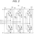
FIG. 2 illustrates a circuit configuration of aconverter 11. -
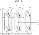
FIG. 3 illustrates a circuit configuration of aninverter 12. -
FIG. 4 illustrates a circuit configuration of a step-up chopper 13. -
FIG. 5 illustrates a configuration of apower conversion unit 101. -
FIG. 6 is a perspective view illustrating the configuration of thepower conversion unit 101. -
FIG. 7 is a right side view illustrating the configuration of thepower conversion unit 101. -
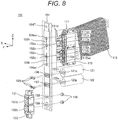
FIG. 8 is an exploded perspective view illustrating a front configuration of thepower conversion unit 101. -
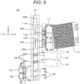
FIG. 9 is an exploded perspective view illustrating a rear configuration of thepower conversion unit 101. -
FIG. 10 is a perspective view illustrating a front configuration of a maincircuit busbar assembly 151. -
FIG. 11 is a perspective view illustrating a rear configuration of the maincircuit busbar assembly 151. -
FIG. 12 is an exploded perspective view illustrating the front configuration of the maincircuit busbar assembly 151. -
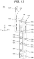
FIG. 13 is an exploded perspective view illustrating the rear configuration of the maincircuit busbar assembly 151. -
FIG. 14 is a diagram illustrating the paths of currents flowing from an external alternating-current terminal 154T in the maincircuit busbar assembly 151 to a negativefuse connection section 159. -
FIG. 15 is a diagram illustrating the paths of currents flowing from a positivefuse connection section 158 in the maincircuit busbar assembly 151 to the external alternating-current terminal 154T. -
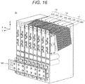
FIG. 16 is a perspective view illustrating a configuration of apower conversion section 2a. -
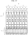
FIG. 17 is a front view illustrating the configuration of thepower conversion section 2a. - An embodiment of the present invention will now be described with reference to the accompanying drawings.
- A UPS (Uninterruptible Power Supply) will be described as the embodiment of the present invention.
-
FIG. 1 illustrates a configuration of the UPS according to the embodiment of the present invention. - The UPS 2 uses a continuous inverter power supply method that is capable of continuously supplying electrical power during power outage. The present invention is applicable to not only the continuous inverter power supply method but also the other power supply methods such as a continuous commercial power supply method.
- During a normal operation, a commercial three-phase alternating-current
power supply voltage 3 supplies electrical power to aload 4 through aconverter 11 and aninverter 12. Theconverter 11 converts commercial three-phase alternating-currentpower supply voltage 3 to a direct-current voltage 5 and supplies the direct-current voltage 5 to theinverter 12. Theinverter 12 converts the direct-current voltage 5 to three-phase alternating-current power 6. This ensures that electrical power equivalent to normal commercial power is steadily supplied to theload 4 as control is exercised by theconverter 11 and theinverter 12 even when the voltage of thecommercial power supply 3 varies due, for instance, to an instantaneous voltage drop. - Meanwhile, in the event of power outage, a
storage battery 14 supplies electrical power to theload 4 through theinverter 12 while theinverter 12 is activated. This enables the UPS 2 to uninterruptedly supply electrical power to theload 4. In the present embodiment, the total voltage of thestorage battery 14 is made sufficiently lower than the direct-current voltage applied to theinverter 12 in order to reduce the cubic volume of theUPS 2. Thus, theUPS 2 according to the present embodiment includes a step-upchopper 13 that raises a low direct-current voltage, which is outputted by discharging thestorage battery 14, to a desired direct-current voltage 5 and outputs the raised direct-current voltage to theinverter 12. If no limitation is imposed on the cubic volume of theUPS 2, theUPS 2 may exclude the step-upchopper 13 and include a high-voltage storage battery 14 capable of supplying a desired direct-current voltage. - A
filter 18 is connected between thecommercial power supply 3 and theconverter 11 in order to shape a sine wave. Thefilter 18 includes, for example, a reactor and a capacitor, which are provided for each phase. One end of the reactor is series-connected to an alternating-current terminal of theconverter 11. The capacitor is parallel-connected to the other end of the reactor. Thefilter 18 is a heavy part and therefore disposed directly below theconverter 11. Afilter 19 is connected between an alternating-current terminal of theinverter 12 and theload 4. Thefilter 19 includes, for example, a reactor and a capacitor, which are provided for each phase. One end of the reactor is series-connected to the alternating-current terminal of theconverter 11. The capacitor is parallel-connected to the other end of the reactor. Thefilter 19 is a heavy part and therefore disposed directly below theinverter 12. Areactor 15 is connected between thestorage battery 14 and an alternating-current terminal of the step-upchopper 13. Thereactor 15 is a heavy part and therefore disposed directly below the step-upchopper 13. - In the subsequent description, the
converter 11, theinverter 12, and the step-upchopper 13 are collectively referred to as thepower conversion section 2a. - The
UPS 2 may further include a cooling mechanism that air-cools thepower conversion section 2a. - In compliance with an instruction, a
bypass circuit 17 bypasses thepower conversion section 2a and directly connects thecommercial power supply 3 to theload 4. Amaintenance bypass circuit 16 is used for the maintenance of thepower conversion section 2a and thebypass circuit 17. In compliance with an instruction, themaintenance bypass circuit 16 bypasses thebypass circuit 17 and directly connects thecommercial power supply 3 to theload 4. -
FIG. 2 illustrates a circuit configuration of theconverter 11. - Three-phase alternating-current power from the
commercial power supply 3 is supplied to alternating-current terminals R, S, T of theconverter 11. In each of R, S, and T phases, the three-phase alternating-current power is rectified by a switching element 21 and rectifyingelement 23 of an upper arm, a switchingelement 22 and rectifyingelement 24 of a lower arm, andcapacitors 120, and then outputted to direct-current terminals P, N. In the present embodiment, an IGBT (Insulated Gate Bipolar Transistor) is used as the switchingelements 21, 22, and a diode is used as the rectifyingelements -
FIG. 3 illustrates a circuit configuration of theinverter 12. - The direct-
current voltage 5, which is obtained by conversion in theconverter 11 or the step-upchopper 13, is supplied to the direct-current terminals P, N of theinverter 12. In each of U, V, and W phases, the direct-current voltage 5 is then converted to the alternating-current power 6 by the switching element 21 and rectifyingelement 23 of the upper arm, the switchingelement 22 and rectifyingelement 24 of the lower arm, and thecapacitors 120, and outputted to alternating-current terminals U, V, W. Three-phase alternating currents outputted from the alternating-current terminals U, V, W are supplied to theload 4. -
FIG. 4 illustrates a circuit configuration of the step-upchopper 13. - The output of the
storage battery 14 is supplied to an input terminal Bat of thereactor 15. While the switchingelement 22 of the lower arm is ON, energy is stored in thereactor 15 connected between the input terminal Bat and an alternating-current terminal C. Subsequently, when the switchingelement 22 of the lower arm turns OFF, thereactor 15 generates a counter-electromotive voltage to turn ON the rectifyingelement 23 of the upper arm. A voltage obtained by adding a direct-current voltage outputted from thestorage battery 14 to the counter-electromotive voltage of thereactor 15 is developed at output terminals P, N of the step-upchopper 13. Thus, a stepped-up direct-current voltage is outputted. - As described above, the
converter 11 andinverter 12 included in theUPS 2 according to the present embodiment both have at least one basic circuit that includespower semiconductor modules 110, thecapacitors 120, apositive fuse 131, and anegative fuse 132. Each of thepower semiconductor modules 110 is a two-level half-bridge circuit that is formed by series-connecting the switching element 21 and rectifyingelement 23 of the upper arm to the switchingelement 22 and rectifyingelement 24 of the lower arm. A three or more multi-level conversion circuit may be used instead of the two-level half-bridge circuit. - In the present embodiment, the basic circuit is implemented by a
power conversion unit 101, andpower conversion units 101 are combined to implement theconverter 11, theinverter 12, and the step-upchopper 13. This not only communizes the types of parts used for thepower conversion section 2a, but also facilitates the assembly and maintenance of thepower conversion section 2a. -
FIG. 5 illustrates a configuration of thepower conversion unit 101. - In the
power conversion unit 101, thepower semiconductor modules 110 are implemented by parallel-connecting a firstpower semiconductor module 111 and a secondpower semiconductor module 112. The firstpower semiconductor module 111 and the secondpower semiconductor module 112 are of a 2-in-1 type and used to form the upper and lower arms, respectively. Further, thecapacitors 120 are implemented by parallel-connecting afirst capacitor 121 and asecond capacitor 122. In this manner, a plurality of power semiconductor modules and a plurality of capacitors are used to implement thepower semiconductor modules 110 and thecapacitors 120 in accordance with electrical power required for thepower conversion unit 101. - Further, in the
power conversion unit 101, thefuse 131 is series-connected to the positive ends of thepower semiconductor modules 110 andcapacitors 120, and thefuse 132 is series-connected to the negative ends of thepower semiconductor modules 110 andcapacitors 120. Asecond terminal 131b of thepositive fuse 131 corresponds to the P terminals of theconverter 11,inverter 12, and step-upchopper 13. Asecond terminal 132b of thenegative fuse 132 corresponds to the N terminals of theconverter 11,inverter 12, and step-upchopper 13. Thefuses power conversion unit 101 increase its reliability in the event of a short-circuit fault. In a situation where a circuit breaker is provided to isolate thepower conversion unit 101, either or both of thefuses - The
power semiconductor modules element 23 of the upper arm and the switchingelement 22 and rectifyingelement 24 of the lower arm. An external alternating-current terminal 154T is connected between the upper and lower arms of thepower semiconductor modules power semiconductor modules gate terminal 111g. A gate terminal of the lowerarm switching elements 22 of thepower semiconductor modules gate terminal 112g. -
FIG. 6 is a perspective view illustrating a configuration of thepower conversion unit 101. - Coordinates of the
UPS 2 are subsequently defined by using an X-axis, a Y-axis, and a Z-axis. The Y-axis direction is a forward direction of theUPS 2. The Z-axis direction is an upward direction of theUPS 2. The X-axis direction is a leftward direction of theUPS 2. Thefuses fuses circuit busbar assembly 151. More specifically, a first terminal 131a of thepositive fuse 131 and a first terminal 132a of thenegative fuse 132 are oriented in the rearward (-Y) direction and connected with a mountingscrew 139 to the maincircuit busbar assembly 151. Meanwhile, a second terminal 131b of thepositive fuse 131 and a second terminal 132b of thenegative fuse 132 are oriented in the forward (+Y) direction. When the above arrangement scheme is employed, the second terminal 131b of thepositive fuse 131 and the second terminal 132b of thenegative fuse 132, which serve as the terminals for coupling the hostpower conversion unit 101 to anotherpower conversion unit 101, are positioned in the front of theUPS 2. This provides increased front accessibility during assembly and maintenance, thereby providing improved workability. As mentioned earlier, thepower conversion unit 101 includes a total of three external terminals, namely, the second terminal 131b of thepositive fuse 131 and the second terminal 132b of thenegative fuse 132, which are connected to a unitcoupling busbar assembly 161 for connecting to anotherpower conversion unit 101, and the external alternating-current terminal 154T provided for the maincircuit busbar assembly 151. -
FIG. 7 is a right side view illustrating the configuration of thepower conversion unit 101. - The
power conversion unit 101 includes thepower semiconductor modules 110, thecapacitors 120, thefuses circuit busbar assembly 151 that electrically connects the foregoing parts. An air-coolingfin 113 is disposed on the rear surface (-Y direction) of thepower semiconductor modules 110 to cool them. Thepower semiconductor modules 110, thecapacitors 120, and thefuses fin 113 flows in the upward (+Z) direction along the rear surface of the maincircuit busbar assembly 151. This arrangement scheme is employed so that the air-cooling 113 is positioned leeward from thecapacitors 120, that is, upward (+Z) from the capacitors, in order to prevent thecapacitors 120 and other parts from receiving heat from the air-coolingfin 113. Further, thefuses fin 113 is disposed in the -Y direction of thepower semiconductor modules 110. However, if, for instance, the air flow path is oriented in the -Y direction, the air-coolingfin 113 may be disposed in the +Z direction of thepower semiconductor modules 110. The direction in which the air-coolingfin 113 is disposed is determined in accordance with the air flow path. Moreover, as thepower semiconductor modules 110 is positioned adjacent to thecapacitors 120, it is possible to reduce parasitic inductance formed on the maincircuit busbar assembly 151, which connects thepower semiconductor modules 110 to thecapacitors 120. Thus, a surge voltage generated upon switching can be reduced. Additionally, the impedance between thepower semiconductor modules 110 in the hostpower conversion unit 101 and thecapacitors 120 in a neighboringpower conversion unit 101 can be minimized. This makes it possible to make effective use of not only thecapacitors 120 in the hostpower conversion unit 101 but also thecapacitors 120 in anotherpower conversion unit 101. As a result, the capacitance of the capacitors that is used for onepower conversion unit 101 can be reduced. In addition, the cubic volume of thepower conversion unit 101 can also be reduced. - The
power semiconductor modules 110 and thecapacitors 120, which have terminals protruding in the forward (+Y) direction, are disposed in the rearward (-Y) direction with respect to the maincircuit busbar assembly 151. This arrangement scheme ensures that all the terminals of thepower semiconductor modules 110 andcapacitors 120 are positioned forward. This makes it easy, for example, to inspect, install, or remove terminal sections during maintenance. -
FIG. 8 is an exploded perspective view illustrating a front configuration of thepower conversion unit 101.FIG. 9 is an exploded perspective view illustrating a rear configuration of thepower conversion unit 101. - In the present embodiment, the
power semiconductor modules 110 are incorporated by parallel-connecting thepower semiconductor module 111 and thepower semiconductor module 112, which are two-level half-bridge circuits (2 in 1). The number of parallel-connected power semiconductor modules in thepower conversion unit 101 is preferably a minimum required number of power semiconductor modules that permit minimum electrical power provided by a model selected for the line-up of a UPS or other power conversion device using thepower conversion unit 101. The reason is that a desired amount of electrical power can be obtained by parallel-connecting thepower conversion units 101 as for a model that requires a larger amount of electrical power. In consideration of the above, the present embodiment is configured so that two power semiconductor modules are connected in parallel. - The
power semiconductor modules positive terminals negative terminals control terminals control terminals gate terminals - The
positive terminals power semiconductor modules 110 are connected to apositive connection terminal 152p in the maincircuit busbar assembly 151. Thenegative terminals power semiconductor modules 110 are connected to anegative connection terminal 153n in the maincircuit busbar assembly 151. The alternating-current terminals 111ac, 112ac in thepower semiconductor modules 110 are connected to a connection terminal 154ac connected to the external alternating-current terminal 154T. Thepositive terminals negative terminals circuit busbar assembly 151 by a welding or other joining method. These terminals may alternatively be connected to the maincircuit busbar assembly 151 by using, for example, screws or clips. - In order to suppress the difference between the distance from the
capacitors 120 to the positive terminal 111p and negative terminal 111n of thepower semiconductor module 111 and the distance from thecapacitors 120 to the positive terminal 112p and negative terminal 112n of thepower semiconductor module 112, the positive terminal 111p and negative terminal 111n of onepower semiconductor module 111 are positioned in a reverse manner from the positive terminal 112p and negative terminal 112n of the otherpower semiconductor module 112. Further, the positive terminal 111p andnegative terminal 111n in thepower semiconductor module 111 face each other in proximity, and the positive terminal 112p andnegative terminal 112n in thepower semiconductor module 112 face each other in proximity. Thus, in the XZ-plane, thepower semiconductor module 112 is positioned in a reverse manner from thepower semiconductor module 111. Using the arrangement scheme reduces the difference in the impedance between thepower semiconductor modules capacitors power semiconductor module 111 and the current flowing in thepower semiconductor module 112. - The positive terminal 121p and negative terminal 121n of the
capacitor 121 are fastened withcapacitor mounting screws 129 to a capacitor joint 156 provided for the maincircuit busbar assembly 151. Similarly, the positive terminal 122p and negative terminal 122n of thecapacitor 122 are fastened with thecapacitor mounting screws 129 to a capacitor joint 157 provided for the maincircuit busbar assembly 151. -
FIG. 10 is a perspective view illustrating a front configuration of the maincircuit busbar assembly 151.FIG. 11 is a perspective view illustrating a rear configuration of the maincircuit busbar assembly 151. -
Capacitor connection sections capacitor joint 156, andcapacitor connection sections capacitor joint 157. Capacitor mounting screw connection sections 156pf, 156nf are disposed opposite thecapacitor connection sections circuit busbar assembly 151, and capacitor mounting screw connection sections 157pf, 157nf are disposed opposite thecapacitor connection sections circuit busbar assembly 151. The positive terminal 121p and negative terminal 121n of thecapacitor 121 are fastened to the rear surface of the capacitor joint 156 by using thecapacitor mounting screws 129 on the front of thecapacitor joint 156. This ensures that the positive terminal 121p and negative terminal 121n of thecapacitor 121 are in contact with thecapacitor connection sections capacitor mounting screws 129 are in contact with the capacitor mounting screw connection sections 156pf, 156nf. Further, the positive terminal 122p and negative terminal 122n of thecapacitor 122 are fastened to the rear surface of the capacitor joint 157 by using thecapacitor mounting screws 129 on the front of thecapacitor joint 157. This ensures that the positive terminal 122p and negative terminal 122n of thecapacitor 122 are in contact with thecapacitor connection sections capacitor mounting screws 129 are in contact with the capacitor mounting screw connection sections 157pf, 157nf. -
Fuse connection sections circuit busbar assembly 151. Fuse mountingscrew connection sections fuse connection sections circuit busbar assembly 151. The first terminal 131a of thepositive fuse 131 is fastened to the front surface of thefuse connection section 158 by using afuse mounting screw 139 on the rear of the fuse mountingscrew connection section 158b. This ensures that the first terminal 131a of thepositive fuse 131 is in contact with thefuse connection section 158, and that thefuse mounting screw 139 is in contact with the fuse mountingscrew connection section 158b. Further, the first terminal 132a of thenegative fuse 132 is fastened to the front surface of thefuse connection section 159 by using thefuse mounting screw 139 on the rear of the fuse mountingscrew connection section 159b. This ensures that the first terminal 132a of thenegative fuse 132 is in contact with thefuse connection section 159, and that thefuse mounting screw 139 is in contact with the fuse mountingscrew connection section 159b. -
FIG. 12 is an exploded perspective view illustrating the front configuration of the maincircuit busbar assembly 151.FIG. 13 is an exploded perspective view illustrating the rear configuration of the maincircuit busbar assembly 151. - The main
circuit busbar assembly 151 includes apositive conductor 152, anegative conductor 153, an alternating-current conductor 154, and aninsulator 155. Thepositive conductor 152, thenegative conductor 153, and the alternating-current conductor 154 are shaped like a flat plate. In order to reduce parasitic inductance generated between thepower semiconductor modules 110 and thecapacitors 120, thepositive conductor 152 and thenegative conductor 153 are stacked via theinsulator 155 so that their opposing faces are parallel and close to each other. This makes it possible to reduce current ripple and impedance in the maincircuit busbar assembly 151 and reduce a surge voltage generated upon switching. Further, theinsulator 155 covers a large portion of the stacked conductors, namely, thepositive conductor 152, thenegative conductor 153, and the alternating-current conductor 154, in such a manner that the conductors are at a predetermined insulating distance from each other. In order to provide improved heat dissipation, the front and rear conductive surfaces of the maincircuit busbar assembly 151 may be exposed while the predetermined insulating distance is maintained. Theinsulator 155 is formed, for instance, of highly-fluid insulative resin. - In the present embodiment, the alternating-
current conductor 154, thepositive conductor 152, and thenegative conductor 153 are disposed in the order named along the rearward (-Y) direction. However, as far as thepositive conductor 152 and thenegative conductor 153 are disposed nearest each other, the parasitic inductance remains unaffected even if the conductors are disposed in a different order. The conductors are formed, for instance, by cutting, bending, or otherwise working a single conductive plate made of copper, aluminum, or other highly conductive material. As an example, thepositive conductor 152 is described below. Thepositive conductor 152 is formed by initially cutting out anopening 152h through which all theterminals power semiconductor modules connection terminal 152p for connecting to thepositive terminals 11p, 112p is left in the plane of a single conductive plate. Theconnection terminal 152p is then formed by bending the portion left in the plane of the conductive plate, which serves as theconnection terminal 152p, 90 degrees in the forward (+Y) direction. The above-described forming method also applies to thenegative conductor 153 and the alternating-current conductor 154. - The
positive conductor 152 includes twoconnection terminals 152p that are respectively connected to thepositive terminals power semiconductor modules 110. Thenegative conductor 153 includes twoconnection terminals 153n that are respectively connected to thenegative terminals power semiconductor modules 110. The alternating-current conductor 154 includes two connection terminals 154ac that are respectively connected to the alternating-current terminals 111ac, 112ac of thepower semiconductor modules 110, and the external alternating-current terminal 154T to be connected to the outside. - At the capacitor joints 156, 157, the
negative terminals capacitors capacitor connection sections negative conductor 153. Further, thecapacitor connection sections positive conductor 152, are disposed so that thepositive terminals capacitors negative conductor 153. Thecapacitor connection sections positive conductor 152 and connected to thepositive conductor 152, for instance, by brazing, soldering, or swaging. Further, thecapacitor connection sections capacitor connection sections capacitor connection sections capacitor mounting screws 129 are driven. Thenegative conductor 153 is provided withopenings capacitor connection sections negative conductor 153. - Further, at the capacitor joints 156, 157, the
capacitor mounting screws 129, which secure the positive terminal 121p of thecapacitor 121 and the positive terminal 122p of thecapacitor 122, are brought into contact with the capacitor connection sections 156pf, 157pf on the front surface of thepositive conductor 152. Moreover, the capacitor connection sections 156nf, 157nf, which protrude in the forward (+Y) direction from thenegative conductor 153, are disposed so that thecapacitor mounting screws 129, which secure thenegative terminal 121n of thecapacitor 121 and thenegative terminal 122n of thecapacitor 122, are brought into contact with a conductor in a virtual plane identical with the front surface of thepositive conductor 152. The capacitor connection sections 156nf, 157nf are separate from thenegative conductor 153 and connected to thenegative conductor 153 by the same method as for thecapacitor connection sections capacitor mounting screws 129 are driven. Thepositive conductor 152 is provided withopenings positive conductor 152. - At the joint between the main
circuit busbar assembly 151 and thefuses positive fuse 131 is brought into contact with thefuse connection section 158 on the front surface of thepositive conductor 152. Further, thefuse connection section 159, which protrudes in the forward (+Y) direction from thenegative conductor 153, is disposed so that the first terminal 132a of thenegative fuse 132 is brought into contact with a conductor in a virtual plane (second virtual plane) identical with the front surface of thepositive conductor 152. Thefuse connection section 159 is separate from thenegative conductor 153 and connected to thenegative conductor 153 by the same method as for thecapacitor connection sections fuse connection section 159 is provided with a hole into which thefuse mounting screw 139 is driven. Thepositive conductor 152 is provided with anopening 159h that prevents the protruding negativefuse connection section 159 from coming into contact with thepositive conductor 152. - As the first terminal 131a of the
positive fuse 131 and the first terminal 132a of thenegative fuse 132 are brought into contact with the maincircuit busbar assembly 151 in the same virtual plane, it is easy to mount thefuses circuit busbar assembly 151. - Further, at the joint between the main
circuit busbar assembly 151 and thefuses fuse mounting screw 139, which secures the first terminal 132a of thenegative fuse 132, is brought into contact with thefuse connection section 158 on the rear surface of thenegative conductor 153. Moreover, thefuse connection section 158b, which protrudes in the rearward (-Y) direction from thenegative conductor 153, is disposed so that thefuse mounting screw 139, which secures the first terminal 131a of thepositive fuse 131, is brought into contact with a conductor in a virtual plane identical with the rear surface of thenegative conductor 153. Thefuse connection section 158b is separate from thepositive conductor 152 and connected to thepositive conductor 153 by the same method as for thecapacitor connection sections fuse connection section 158b is provided with a hole into which thefuse mounting screw 139 is driven. Thenegative conductor 153 is provided with anopening 158h that prevents the protruding positivefuse connection section 158b from coming into contact with thenegative conductor 153. - From up to down (in the -Z direction), the external alternating-
current terminal 154T, thepower semiconductor module 111, thepower semiconductor module 112, thecapacitor 121, thecapacitor 122, and thefuse connection sections power conversion unit 101. Further, thepower semiconductor modules power semiconductor module 112 is positioned adjacent to and in the downward (-Z direction) of thepower semiconductor module 111. This reduces the X-direction size of thepower conversion unit 101 as compared to the case where the two power semiconductor modules are arranged in a horizontal direction. On the surface (XZ plane) of the maincircuit busbar assembly 151, the longitudinal direction of thepower semiconductor modules circuit busbar assembly 151. If, for example, the distance from the alternating-current terminal 111ac in thepower semiconductor module 111 to the positive terminal 111p and thenegative terminal 111n and the distance from the alternating-current terminal 112ac in thepower semiconductor module 112 to the positive terminal 112p and thenegative terminal 112n are the terminal-to-terminal distance, the terminal-to-terminal distance is longer than the widths (X-direction length) of thepower semiconductor modules power conversion unit 101. - As the
power conversion unit 101 is configured as described above, it is possible to reduce the footprint of a power conversion device, such as theUPS 2. - As the
power semiconductor modules power semiconductor module 111 is different from the path of a current flowing in thepower semiconductor module 112. Therefore, the currents might be imbalanced. A configuration for avoiding such an imbalance is described below. - First of all, a case where a current flows from the alternating-current side of the main
circuit busbar assembly 151 to the direct-current side will be described. -
FIG. 14 is a diagram illustrating the paths of currents flowing from the external alternating-current terminal 154T in the maincircuit busbar assembly 151 to the negativefuse connection section 159. - For zoning purposes, line segments h1 to h5 are defined with reference to the locations of the external alternating-
current terminal 154T existing in the longitudinal direction of the maincircuit busbar assembly 151, the alternating-current terminal 111ac of the firstpower semiconductor module 111, the positive andnegative terminals power semiconductor module 111, the positive andnegative terminals power semiconductor module 112, the alternating-current terminal 112ac of the secondpower semiconductor module 112, and thefuse connection section - Here, as a steady state, let us assume a situation where the IGBT of the lower arm in each of the
power semiconductor modules current terminal 154T. In this state, the current flows from the external alternating-current terminal 154T through the alternating-current conductor 154 to the IGBT of the lower arm in thepower semiconductor modules negative conductor 153, and to the negativefuse connection section 159 in the order named. For purposes of explanation, the current path is divided intopath 1 andpath 2.Path 1 is the path of the current flowing through the firstpower semiconductor module 111.Path 2 is the path of the current flowing through the secondpower semiconductor module 112. - Here, it is assumed that the
positive conductor 152, thenegative conductor 153, and the alternating-current conductor 154 have the same impedance per unit length, and that the impedance is Zc. Further, it is assumed that thepower semiconductor modules path 1 and the impedance Z2 ofpath 2 are expressed by the following equations by using line segments h1 to h5.

- From Equations (1) and (2), the imbalance between the impedances Z2 - Z1 is expressed by the following equation.

- As indicated in Equation (3), the imbalance between the impedances of
paths power semiconductor module 112 is oriented in an opposite direction from thepower semiconductor module 111. - A current imbalance arises in accordance with the ratio of an impedance imbalance to the impedance of all paths. Therefore, the current imbalance can be reduced when the imbalance between the path lengths h2 + h4 is sufficiently smaller than the total path length. That is to say, the following relational expression is obtained.

- In other words, h2 + h4 is sufficiently smaller than a value obtained by subtracting h2 + h4 from the distance between the external alternating-
current terminal 154T and thefuse connection sections power semiconductor module 111 and the secondpower semiconductor module 112 need to be positioned close to each other. Therefore, h3 needs to be short. Thus, Equation (4) signifies that h1 and h5 should be sufficiently longer than h2 and h4. Consequently, when the external alternating-current terminal 154T and thefuse connection section circuit busbar assembly 151, the currents flowing in the firstpower semiconductor module 111 and the secondpower semiconductor module 112 can be balanced in the steady state. It should be noted that h2 and h4 may be equal. - Meanwhile, if Equation (4) is not sufficiently satisfied due, for instance, to dimensional limitations on the overall structure of a power conversion device, the current imbalance becomes great. In such an instance, the imbalance between path lengths can be reduced by adjusting the conductor thickness of an imbalanced alternating-
current conductor 154. - Here, it is assumed that the
positive conductor 152 and thenegative conductor 153 are equal in thickness, and that the thickness of the alternating-current conductor 154 is n times the thickness of thepositive conductor 152 andnegative conductor 153. The impedance Z1 ofpath 1 and the impedance Z2 ofpath 2 are expressed by the following equations.

- From Equations (5) and (6), n for equalizing Z1 and Z2 is expressed by the following equation.

- As described above, when the ratio of the thickness of the
positive conductor 152 andnegative conductor 153 to the thickness of the alternating-current conductor 154 is equal to n, which is expressed by Equation (7), the impedance imbalance can be suppressed to avoid the imbalance between the current flowing inpath 1 and the current flowing inpath 2. - Next, a case where a current flows from the direct-current side of the main
circuit busbar assembly 151 to the alternating-current side will be described. -
FIG. 15 is a diagram illustrating the paths of currents flowing from the positivefuse connection section 158 in the maincircuit busbar assembly 151 to the external alternating-current terminal 154T. - Here, as a steady state, let us assume a situation where the IGBT of the upper arm in each of the
power semiconductor modules current terminal 154T. In this state, the current flows from thefuse connection section 158 through thepositive conductor 152 to the IGBT of the upper arm in thepower semiconductor modules current conductor 154, and to the external alternating-current terminal 154T in the order named. For purposes of explanation, the current path is divided intopath 3 andpath 4.Path 3 is the path of the current flowing through the firstpower semiconductor module 111.Path 4 is the path of the current flowing through the secondpower semiconductor module 112. In this instance,path 3 is equal in length topath 1, andpath 4 is equal in length topath 2. Therefore, when thepositive conductor 152, thenegative conductor 153, and the alternating-current conductor 154 are equal in thickness, the conditions for the length of each zone are as expressed by Equation (4) above. Further, the conditions for a case where the alternating-current conductor 154 is different in thickness from thepositive conductor 152 and thenegative conductor 153 are as expressed by Equation (7) above. -
FIG. 16 is a perspective view illustrating a configuration of thepower conversion section 2a. - The
power conversion section 2a is disposed in a housing (not shown) of theUPS 2. An open/close door (not shown), which is to be opened for the maintenance of theUPS 2, is attached to the front surface of the housing of theUPS 2, that is, positioned in the Y-axis direction of thepower conversion section 2a. Opening the open/close door makes it easy to access the front surface of thepower conversion section 2a. - The
power conversion section 2a includes a plurality ofpower conversion units 101, which are disposed in the X-axis direction. Theconverter 11 includes three power conversion units, which respectively correspond to the three phases of commercial power. Similarly, theinverter 12 includes threepower conversion units 101, which respectively correspond the three phases. - The step-up
chopper 13 includes twopower conversion units 101, which are connected in parallel. The step-upchopper 13 may be formed of onepower conversion unit 101. If the rated power of thepower semiconductor modules 110 included in thepower conversion unit 101 is exceeded by electrical power required for the step-upchopper 13, Npower conversion units 101 are connected in parallel to increase the permissible power N-fold. For similar purposes, theconverter 11 and theinverter 12 may each include, as needed, a plurality of parallel-connectedpower conversion units 101 per phase. - The
power conversion units 101 in thepower conversion section 2a are parallel-connected through the unitcoupling busbar assembly 161. The longitudinal direction of each of thepower conversion units 101 is the Z direction, and thepower conversion units 101 are disposed in the X direction. The longitudinal direction of the unitcoupling busbar assembly 161 is the X direction, and the unitcoupling busbar assembly 161 is disposed in the +Y direction of thepower conversion units 101. That is to say, the longitudinal direction of each of thepower conversion units 101 crosses the longitudinal direction of the unitcoupling busbar assembly 161. Consequently, thepower conversion units 101 can be efficiently disposed within a limited cubic volume. - The unit
coupling busbar assembly 161 is assembled, by using mountingscrews 169, to the second terminal 131b of thepositive fuse 131 and the second terminal 132b of thenegative fuse 132, which are mounted on the lower front surface of eachpower conversion unit 101. -
FIG. 17 is a front view illustrating the configuration of thepower conversion section 2a. - The external alternating-
current terminals 154T disposed on the upper ends of thepower conversion units 101 respectively correspond to the R, S, and T terminals of theconverter 11, the U, V, and W terminals of theinverter 12, and the C terminals (common) of the step-upchopper 13. Two terminals are disposed on the left end of the unitcoupling busbar assembly 161. The upper one of these terminals corresponds to the P terminals of theconverter 11,inverter 12, and step-upchopper 13, and the lower one corresponds to the N terminals of theconverter 11,inverter 12, and step-upchopper 13. - When the configuration according to the above-described embodiment is employed to parallel-connect an appropriate number of
power conversion units 101 in accordance with a desired amount of electrical power and the number of phases, various power conversion devices, such as theconverter 11, theinverter 12, and the step-upchopper 13, can be configured in an arbitrary manner. When thepower conversion unit 101 is manufactured as a minimum configuration unit, the parts for various power conversion devices can be communized to achieve cost reduction. Further, when the communizedpower conversion units 101 are employed and disposed in parallel, the resulting layout is in good order. This increases the ease of unit-to-unit connection wiring and provides improved overall assemblability. Moreover, the terminals, capacitor terminals, and fuse terminals for the power semiconductor modules included in thepower conversion unit 101 and the unitcoupling busbar assembly 161 for connecting the power conversion units are on the front surface of the power conversion device. This improves front accessibility during assembly and maintenance, thereby providing increased workability. - A method of manufacturing the
power conversion section 2a will now be described. First of all, a manufacturer disposes a plurality ofpower conversion units 101 in the +X direction and disposes the unitcoupling busbar assembly 161 in the +Y direction with respect to thepower conversion units 101. Subsequently, the manufacturer connects a plurality ofpositive conductors 152, which are respectively included in thepower conversion units 101, through a positive conductor 162 included in the unitcoupling busbar assembly 161, and connects a plurality of thenegative conductors 153, which are respectively included in thepower conversion units 101, through a negative conductor 163 included in the unitcoupling busbar assembly 161. In this manner, thepower conversion section 2a is manufactured. Further, the manufacturer can manufacture, for example, theconverter 11, theinverter 12, and the step-upchopper 13 by using thepower conversion units 101. Moreover, the manufacturer can manufacture theUPS 2 by connecting, for example, thestorage battery 14, themaintenance bypass circuit 16, and thebypass circuit 17 to a plurality of alternating-current terminals 154T, which are respectively included in thepower conversion units 101. - In the
power conversion unit 101, from up to down (in the -Z direction), external direct-current terminals including an external positive terminal and an external negative terminal, thepower semiconductor module 111, thepower semiconductor module 112, thecapacitor 121, thecapacitor 122, and the external alternating-current terminal 154T may be disposed in the order named. In such an instance, the external direct-current terminals are disposed on the upper end of the maincircuit busbar assembly 151, and the external alternating-current terminal 154T is disposed on the lower end of the maincircuit busbar assembly 151. In this case, heavy parts, such as the reactor connected to the external alternating-current terminal 154T, are disposed below thepower conversion unit 101. Therefore, the distance between the external alternating-current terminal and the heavy parts can be shortened to reduce the impedance. - Terms used in this document will now be explained. A power conversion unit corresponds, for example, to the
power conversion unit 101. A positive conductor corresponds, for example, to thepositive conductor 152. A negative conductor corresponds, for example, to thenegative conductor 153. An alternating-current conductor corresponds, for example, to the alternating-current conductor 154. A circuit connection section corresponds, for example, to the maincircuit busbar assembly 151. A capacitor corresponds, for example, to thecapacitors 120. A positive connection conductor corresponds, for example, to the positive conductor 162. A negative connection conductor corresponds, for example, to the negative conductor 163. Two two-level half-bridge circuits correspond, for example, to thepower semiconductor modules capacitors fuse 131. A negative fuse corresponds, for example, to thefuse 132. A power conversion device corresponds, for example, to theconverter 11, theinverter 12, the step-upchopper 13, thepower conversion section 2a, and theUPS 2. A first power semiconductor module corresponds, for example, to thepower semiconductor module 111. A second power semiconductor module corresponds, for example, to thepower semiconductor module 112. An external positive terminal corresponds, for example, to thefuse connection section 158. An external negative terminal corresponds, for example, to thefuse connection section 159. An external alternating-current terminal corresponds, for example, to the external alternating-current terminal 154T. A first direct-current terminal corresponds, for example, to the positive terminal 111p and thenegative terminal 111n. A first positive terminal corresponds, for example, to thepositive terminal 111p. A first negative terminal corresponds, for example, to thenegative terminal 111n. A first alternating-current terminal corresponds, for example, to the alternating-current terminal 111ac. A second direct-current terminal corresponds, for example, to the positive terminal 112p and thenegative terminal 112n. A second positive terminal corresponds, for example, to thepositive terminal 112p. A second negative terminal corresponds, for example, to thenegative terminal 112n. A second alternating-current terminal corresponds, for example, to the alternating-current terminal 112ac. A specific direction corresponds, for example, to the -Z direction. An array direction corresponds, for example, to the X direction. a corresponds, for example, to h2. b corresponds, for example, to h4. c corresponds, for example, to h3. - The present invention is not limited to the above-described embodiment, and various modifications may be made without departing from the spirit of the present invention.
-
- 1: Power conversion device,
- 2: UPS (Uninterruptible Power Supply),
- 11: Converter,
- 12: Inverter,
- 13: Step-up chopper,
- 101: Power conversion unit,
- 110: Power semiconductor modules,
- 111, 112: Power semiconductor module,
- 113: Air-cooling fin,
- 120: Capacitors,
- 121, 122: Capacitor,
- 131, 132: Fuse,
- 151: Main circuit busbar assembly,
- 152: Positive conductor,
- 153: Negative conductor,
- 154: Alternating-current conductor,
- 154T: External alternating-current terminal,
- 155: Insulator,
- 161: Unit coupling busbar assembly,
- 162: Positive conductor,
- 162T: External positive terminal,
- 163: Negative conductor,
- 163T: External negative terminal,
- 164: Insulator.
Claims (14)
- A power conversion unit comprising:a circuit connection section that includes a positive conductor having an external positive terminal, a negative conductor having an external negative terminal, and an alternating-current conductor having an external alternating-current terminal;a first power semiconductor module that is connected to the positive conductor, the negative conductor, and the alternating-current conductor;a second power semiconductor module that is connected to the positive conductor, the negative conductor, and the alternating-current conductor; anda capacitor that is connected to the positive conductor and the negative conductor;wherein the first power semiconductor module includes a first direct-current terminal and a first alternating-current terminal, the first direct-current terminal having a first positive terminal connected to the positive conductor and a first negative terminal connected to the negative conductor, the first alternating-current terminal being connected to the alternating-current conductor;wherein the second power semiconductor module includes a second direct-current terminal and a second alternating-current terminal, the second direct-current terminal having a second positive terminal connected to the positive conductor and a second negative terminal connected to the negative conductor, the second alternating-current terminal being connected to the alternating-current conductor;wherein the external alternating-current terminal, the first power semiconductor module, the second power semiconductor module, the capacitor, and an external direct-current terminal including the external positive terminal and the external negative terminal are arrayed on a straight line extending in the longitudinal direction of the circuit connection section;wherein the external alternating-current terminal is disposed at one longitudinal end of the circuit connection section; andwherein the external direct-current terminal is disposed at the other longitudinal end of the circuit connection section.
- The power conversion unit according to claim 1,
wherein the first direct-current terminal, the first alternating-current terminal, the second direct-current terminal, and the second alternating-current terminal are arrayed on the straight line;
wherein the first direct-current terminal is disposed in a specific direction with respect to the first alternating-current terminal; and
wherein the second direct-current terminal is disposed in a direction opposite to the specific direction with respect to the second alternating-current terminal. - The power conversion unit according to claim 1 or 2,
wherein the positive conductor, the negative conductor, and the alternating-current conductor are shaped like a flat plate; and
wherein the positive conductor, the negative conductor, and the alternating-current conductor are stacked together via an insulator. - The power conversion unit according to any one of claims 1 to 3,
wherein the distance between the first alternating-current terminal and the first direct-current terminal and the distance between the second alternating-current terminal and the second direct-current terminal are greater than the transverse length of a flat plate of the circuit connection section. - The power conversion unit according to any one of claims 2 to 4,
wherein the positive conductor and the negative conductor have a predetermined thickness;
wherein the thickness of the alternating-current conductor is greater than the predetermined thickness; and
wherein the ratio n of the thickness of the alternating-current conductor to the predetermined thickness is expressed by using the distance a between the first alternating-current terminal and the first direct-current terminal, the distance b between the second direct-current terminal and the second alternating-current terminal, and the distance c between the first direct-current terminal and the second direct-current terminal. - The power conversion unit according to claim 5,
wherein the relationship between n, a, b, and c is expressed by n = 1 + (a + b)/c. - The power conversion unit according to any one of claims 1 to 4,
wherein the positive conductor, the negative conductor, and the alternating-current conductor are equal in thickness; and
wherein the sum of the distance between the first alternating-current terminal and the first direct-current terminal and the distance between the second direct-current terminal and the second alternating-current terminal is smaller than a value obtained by subtracting the sum from the distance between the external alternating-current terminal and the external direct-current terminal. - The power conversion unit according to any one of claims 1 to 7,
wherein the external alternating-current terminal, the first power semiconductor module, the second power semiconductor module, the capacitor, and the external direct-current terminal are sequentially disposed on the straight line. - The power conversion unit according to any one of claims 1 to 7,
wherein the external direct-current terminal, the first power semiconductor module, the second power semiconductor module, the capacitor, and the external alternating-current terminal are sequentially disposed on the straight line. - The power conversion unit according to any one of claims 1 to 9,
wherein the first negative terminal is disposed in an array direction that is the transverse direction of the circuit connection section with respect to the first positive terminal; and
wherein the second negative terminal is disposed in a direction opposite to the array direction with respect to the second positive terminal. - The power conversion unit according to any one of claims 1 to 10,
wherein the capacitor includes two capacitors; and
wherein the two capacitors are disposed on the straight line. - The power conversion unit according to any one of claims 1 to 11,
wherein the first power semiconductor module and the second power semiconductor module each include a two-level half-bridge circuit. - The power conversion unit according to any one of claims 1 to 12, further comprising:at least one of a positive fuse and a negative fuse, the positive fuse being a fuse connected to the external positive terminal, the negative fuse being a fuse connected to the external negative terminal.
- A power conversion device comprising:a plurality of power conversion units;wherein the power conversion units each includea circuit connection section including a positive conductor having an external positive terminal, a negative conductor having an external negative terminal, and an alternating-current conductor having an external alternating-current terminal,a first power semiconductor module including a first positive terminal connected to the positive conductor, a first direct-current terminal having a first negative terminal connected to the negative conductor, and a first alternating-current terminal connected to the alternating-current conductor,a second power semiconductor module including a second positive terminal connected to the positive conductor, a second direct-current terminal having a second negative terminal connected to the negative conductor, and a second alternating-current terminal connected to the alternating-current conductor, anda capacitor that is connected to the positive conductor and the negative conductor;wherein the external alternating-current terminal, the first power semiconductor module, the second power semiconductor module, the capacitor, and an external direct-current terminal including the external positive terminal and the external negative terminal are arrayed on a straight line extending in the longitudinal direction of the circuit connection section;wherein the external alternating-current terminal is disposed at one longitudinal end of the circuit connection section; andwherein the external direct-current terminal is disposed at the other longitudinal end of the circuit connection section.
Applications Claiming Priority (2)
| Application Number | Priority Date | Filing Date | Title |
|---|---|---|---|
| JP2014194820A JP5778840B1 (en) | 2014-09-25 | 2014-09-25 | Power conversion unit and power conversion device |
| PCT/JP2015/056027 WO2016047164A1 (en) | 2014-09-25 | 2015-03-02 | Power conversion unit and power conversion device |
Publications (3)
| Publication Number | Publication Date |
|---|---|
| EP3136580A1 true EP3136580A1 (en) | 2017-03-01 |
| EP3136580A4 EP3136580A4 (en) | 2018-01-24 |
| EP3136580B1 EP3136580B1 (en) | 2019-09-04 |
Family
ID=54192761
Family Applications (1)
| Application Number | Title | Priority Date | Filing Date |
|---|---|---|---|
| EP15843572.7A Active EP3136580B1 (en) | 2014-09-25 | 2015-03-02 | Power conversion unit and power conversion device |
Country Status (5)
| Country | Link |
|---|---|
| US (1) | US9906154B2 (en) |
| EP (1) | EP3136580B1 (en) |
| JP (1) | JP5778840B1 (en) |
| CN (1) | CN105981284B (en) |
| WO (1) | WO2016047164A1 (en) |
Families Citing this family (11)
| Publication number | Priority date | Publication date | Assignee | Title |
|---|---|---|---|---|
| WO2015145679A1 (en) * | 2014-03-27 | 2015-10-01 | 株式会社日立製作所 | Power conversion unit, power conversion apparatus, and power conversion apparatus manufacturing method |
| DE112014007088B4 (en) * | 2014-10-22 | 2023-12-21 | Mitsubishi Electric Corporation | Power conversion device with a filter capacitor |
| JP6174824B2 (en) * | 2015-04-20 | 2017-08-02 | 三菱電機株式会社 | Power converter |
| US10137798B2 (en) * | 2015-08-04 | 2018-11-27 | Ford Global Technologies, Llc | Busbars for a power module assembly |
| US10432106B2 (en) * | 2016-01-21 | 2019-10-01 | Mitsubishi Electric Corporation | Power conversion device |
| JP6646819B2 (en) * | 2016-03-25 | 2020-02-14 | パナソニックIpマネジメント株式会社 | Switching power supply |
| JP6715685B2 (en) * | 2016-06-07 | 2020-07-01 | 株式会社日立製作所 | Power conversion device and power conversion method |
| US10587203B2 (en) * | 2016-11-17 | 2020-03-10 | Toshiba Mitsubishi-Electric Industrial Systems Corporation | Power conversion apparatus |
| CN111357106B (en) * | 2017-11-21 | 2023-11-14 | 三菱电机株式会社 | Semiconductor modules, power conversion devices and mobile bodies |
| RU2741318C1 (en) * | 2018-01-26 | 2021-01-25 | Хитачи, Лтд. | Power conversion device and electric railway vehicle equipped with power conversion device |
| JP7074028B2 (en) * | 2018-11-13 | 2022-05-24 | トヨタ自動車株式会社 | Power converter |
Family Cites Families (12)
| Publication number | Priority date | Publication date | Assignee | Title |
|---|---|---|---|---|
| JPH01186176A (en) | 1988-01-21 | 1989-07-25 | Fuji Electric Co Ltd | Transistor inverter device |
| WO2004105220A2 (en) | 2003-05-16 | 2004-12-02 | Ballard Power Systems Corporation | Power module system |
| WO2009115124A1 (en) * | 2008-03-20 | 2009-09-24 | Abb Technology Ag | A voltage source converter |
| CN201341084Y (en) * | 2008-11-12 | 2009-11-04 | 中国北车股份有限公司大连电力牵引研发中心 | Power module main body device of current transformer |
| CA2751034C (en) | 2009-02-24 | 2015-02-17 | Toshiki Tatsuta | Semiconductor stack and power converter using the same |
| JP5528299B2 (en) * | 2010-10-28 | 2014-06-25 | 三菱電機株式会社 | Power converter |
| TW201233038A (en) * | 2011-01-19 | 2012-08-01 | Sanyo Electric Co | Inverter device and a mobile equpment carrying the inverter device |
| JP5664602B2 (en) | 2012-07-10 | 2015-02-04 | ウシオ電機株式会社 | Short arc type mercury lamp |
| JP5830480B2 (en) * | 2013-03-05 | 2015-12-09 | 日立オートモティブシステムズ株式会社 | Wiring board and power conversion device using the same |
| JP6182021B2 (en) * | 2013-08-28 | 2017-08-16 | 株式会社日立製作所 | Power converter |
| JP6208326B2 (en) * | 2014-03-10 | 2017-10-04 | 株式会社日立製作所 | Power conversion unit, power conversion device, and power conversion method |
| WO2015145679A1 (en) * | 2014-03-27 | 2015-10-01 | 株式会社日立製作所 | Power conversion unit, power conversion apparatus, and power conversion apparatus manufacturing method |
-
2014
- 2014-09-25 JP JP2014194820A patent/JP5778840B1/en not_active Expired - Fee Related
-
2015
- 2015-03-02 WO PCT/JP2015/056027 patent/WO2016047164A1/en not_active Ceased
- 2015-03-02 CN CN201580007585.2A patent/CN105981284B/en not_active Expired - Fee Related
- 2015-03-02 US US15/113,850 patent/US9906154B2/en active Active
- 2015-03-02 EP EP15843572.7A patent/EP3136580B1/en active Active
Also Published As
| Publication number | Publication date |
|---|---|
| JP2016067133A (en) | 2016-04-28 |
| EP3136580A4 (en) | 2018-01-24 |
| WO2016047164A1 (en) | 2016-03-31 |
| CN105981284B (en) | 2018-07-06 |
| EP3136580B1 (en) | 2019-09-04 |
| CN105981284A (en) | 2016-09-28 |
| JP5778840B1 (en) | 2015-09-16 |
| US20170040906A1 (en) | 2017-02-09 |
| US9906154B2 (en) | 2018-02-27 |
Similar Documents
| Publication | Publication Date | Title |
|---|---|---|
| EP3136580B1 (en) | Power conversion unit and power conversion device | |
| JP6346661B2 (en) | Power conversion unit, power conversion device, and method of manufacturing power conversion device | |
| US9300221B2 (en) | Power converter including smoothing capacitor and discharge resistor | |
| JPWO2015136593A1 (en) | Power conversion unit, power conversion device, and power conversion method | |
| EP3528605B1 (en) | Compact design of multilevel power converter systems | |
| US11570884B2 (en) | Relay arrangement with improved heat dissipation and converter device having a relay arrangement of this kind | |
| US12453031B2 (en) | Power conversion device | |
| CN112993695B (en) | Vehicle interleaved bus bar | |
| JP5894321B1 (en) | Power conversion unit and power conversion device | |
| JP6469837B2 (en) | Power conversion unit and power conversion device | |
| KR102724180B1 (en) | High-efficiency heat dissipation module and battery cycler having with the same | |
| KR102660465B1 (en) | Battery cycler having sub-boards | |
| JP2020202619A (en) | Power converter | |
| KR101611885B1 (en) | Inverter Stack | |
| JP7215042B2 (en) | inverter |
Legal Events
| Date | Code | Title | Description |
|---|---|---|---|
| STAA | Information on the status of an ep patent application or granted ep patent |
Free format text: STATUS: THE INTERNATIONAL PUBLICATION HAS BEEN MADE |
|
| PUAI | Public reference made under article 153(3) epc to a published international application that has entered the european phase |
Free format text: ORIGINAL CODE: 0009012 |
|
| STAA | Information on the status of an ep patent application or granted ep patent |
Free format text: STATUS: REQUEST FOR EXAMINATION WAS MADE |
|
| 17P | Request for examination filed |
Effective date: 20161125 |
|
| AK | Designated contracting states |
Kind code of ref document: A1 Designated state(s): AL AT BE BG CH CY CZ DE DK EE ES FI FR GB GR HR HU IE IS IT LI LT LU LV MC MK MT NL NO PL PT RO RS SE SI SK SM TR |
|
| AX | Request for extension of the european patent |
Extension state: BA ME |
|
| DAV | Request for validation of the european patent (deleted) | ||
| DAX | Request for extension of the european patent (deleted) | ||
| A4 | Supplementary search report drawn up and despatched |
Effective date: 20180102 |
|
| RIC1 | Information provided on ipc code assigned before grant |
Ipc: H02M 7/48 20070101AFI20171219BHEP |
|
| STAA | Information on the status of an ep patent application or granted ep patent |
Free format text: STATUS: EXAMINATION IS IN PROGRESS |
|
| 17Q | First examination report despatched |
Effective date: 20180606 |
|
| GRAP | Despatch of communication of intention to grant a patent |
Free format text: ORIGINAL CODE: EPIDOSNIGR1 |
|
| STAA | Information on the status of an ep patent application or granted ep patent |
Free format text: STATUS: GRANT OF PATENT IS INTENDED |
|
| INTG | Intention to grant announced |
Effective date: 20190401 |
|
| GRAS | Grant fee paid |
Free format text: ORIGINAL CODE: EPIDOSNIGR3 |
|
| GRAA | (expected) grant |
Free format text: ORIGINAL CODE: 0009210 |
|
| STAA | Information on the status of an ep patent application or granted ep patent |
Free format text: STATUS: THE PATENT HAS BEEN GRANTED |
|
| AK | Designated contracting states |
Kind code of ref document: B1 Designated state(s): AL AT BE BG CH CY CZ DE DK EE ES FI FR GB GR HR HU IE IS IT LI LT LU LV MC MK MT NL NO PL PT RO RS SE SI SK SM TR |
|
| REG | Reference to a national code |
Ref country code: GB Ref legal event code: FG4D |
|
| REG | Reference to a national code |
Ref country code: CH Ref legal event code: EP |
|
| REG | Reference to a national code |
Ref country code: AT Ref legal event code: REF Ref document number: 1176776 Country of ref document: AT Kind code of ref document: T Effective date: 20190915 |
|
| REG | Reference to a national code |
Ref country code: DE Ref legal event code: R096 Ref document number: 602015037447 Country of ref document: DE |
|
| REG | Reference to a national code |
Ref country code: IE Ref legal event code: FG4D |
|
| REG | Reference to a national code |
Ref country code: NL Ref legal event code: MP Effective date: 20190904 |
|
| REG | Reference to a national code |
Ref country code: LT Ref legal event code: MG4D |
|
| PG25 | Lapsed in a contracting state [announced via postgrant information from national office to epo] |
Ref country code: NO Free format text: LAPSE BECAUSE OF FAILURE TO SUBMIT A TRANSLATION OF THE DESCRIPTION OR TO PAY THE FEE WITHIN THE PRESCRIBED TIME-LIMIT Effective date: 20191204 Ref country code: FI Free format text: LAPSE BECAUSE OF FAILURE TO SUBMIT A TRANSLATION OF THE DESCRIPTION OR TO PAY THE FEE WITHIN THE PRESCRIBED TIME-LIMIT Effective date: 20190904 Ref country code: SE Free format text: LAPSE BECAUSE OF FAILURE TO SUBMIT A TRANSLATION OF THE DESCRIPTION OR TO PAY THE FEE WITHIN THE PRESCRIBED TIME-LIMIT Effective date: 20190904 Ref country code: HR Free format text: LAPSE BECAUSE OF FAILURE TO SUBMIT A TRANSLATION OF THE DESCRIPTION OR TO PAY THE FEE WITHIN THE PRESCRIBED TIME-LIMIT Effective date: 20190904 Ref country code: BG Free format text: LAPSE BECAUSE OF FAILURE TO SUBMIT A TRANSLATION OF THE DESCRIPTION OR TO PAY THE FEE WITHIN THE PRESCRIBED TIME-LIMIT Effective date: 20191204 Ref country code: LT Free format text: LAPSE BECAUSE OF FAILURE TO SUBMIT A TRANSLATION OF THE DESCRIPTION OR TO PAY THE FEE WITHIN THE PRESCRIBED TIME-LIMIT Effective date: 20190904 |
|
| PG25 | Lapsed in a contracting state [announced via postgrant information from national office to epo] |
Ref country code: AL Free format text: LAPSE BECAUSE OF FAILURE TO SUBMIT A TRANSLATION OF THE DESCRIPTION OR TO PAY THE FEE WITHIN THE PRESCRIBED TIME-LIMIT Effective date: 20190904 Ref country code: LV Free format text: LAPSE BECAUSE OF FAILURE TO SUBMIT A TRANSLATION OF THE DESCRIPTION OR TO PAY THE FEE WITHIN THE PRESCRIBED TIME-LIMIT Effective date: 20190904 Ref country code: RS Free format text: LAPSE BECAUSE OF FAILURE TO SUBMIT A TRANSLATION OF THE DESCRIPTION OR TO PAY THE FEE WITHIN THE PRESCRIBED TIME-LIMIT Effective date: 20190904 Ref country code: GR Free format text: LAPSE BECAUSE OF FAILURE TO SUBMIT A TRANSLATION OF THE DESCRIPTION OR TO PAY THE FEE WITHIN THE PRESCRIBED TIME-LIMIT Effective date: 20191205 Ref country code: ES Free format text: LAPSE BECAUSE OF FAILURE TO SUBMIT A TRANSLATION OF THE DESCRIPTION OR TO PAY THE FEE WITHIN THE PRESCRIBED TIME-LIMIT Effective date: 20190904 |
|
| REG | Reference to a national code |
Ref country code: AT Ref legal event code: MK05 Ref document number: 1176776 Country of ref document: AT Kind code of ref document: T Effective date: 20190904 |
|
| PG25 | Lapsed in a contracting state [announced via postgrant information from national office to epo] |
Ref country code: RO Free format text: LAPSE BECAUSE OF FAILURE TO SUBMIT A TRANSLATION OF THE DESCRIPTION OR TO PAY THE FEE WITHIN THE PRESCRIBED TIME-LIMIT Effective date: 20190904 Ref country code: PL Free format text: LAPSE BECAUSE OF FAILURE TO SUBMIT A TRANSLATION OF THE DESCRIPTION OR TO PAY THE FEE WITHIN THE PRESCRIBED TIME-LIMIT Effective date: 20190904 Ref country code: PT Free format text: LAPSE BECAUSE OF FAILURE TO SUBMIT A TRANSLATION OF THE DESCRIPTION OR TO PAY THE FEE WITHIN THE PRESCRIBED TIME-LIMIT Effective date: 20200106 Ref country code: NL Free format text: LAPSE BECAUSE OF FAILURE TO SUBMIT A TRANSLATION OF THE DESCRIPTION OR TO PAY THE FEE WITHIN THE PRESCRIBED TIME-LIMIT Effective date: 20190904 Ref country code: AT Free format text: LAPSE BECAUSE OF FAILURE TO SUBMIT A TRANSLATION OF THE DESCRIPTION OR TO PAY THE FEE WITHIN THE PRESCRIBED TIME-LIMIT Effective date: 20190904 Ref country code: IT Free format text: LAPSE BECAUSE OF FAILURE TO SUBMIT A TRANSLATION OF THE DESCRIPTION OR TO PAY THE FEE WITHIN THE PRESCRIBED TIME-LIMIT Effective date: 20190904 Ref country code: EE Free format text: LAPSE BECAUSE OF FAILURE TO SUBMIT A TRANSLATION OF THE DESCRIPTION OR TO PAY THE FEE WITHIN THE PRESCRIBED TIME-LIMIT Effective date: 20190904 |
|
| PG25 | Lapsed in a contracting state [announced via postgrant information from national office to epo] |
Ref country code: CZ Free format text: LAPSE BECAUSE OF FAILURE TO SUBMIT A TRANSLATION OF THE DESCRIPTION OR TO PAY THE FEE WITHIN THE PRESCRIBED TIME-LIMIT Effective date: 20190904 Ref country code: IS Free format text: LAPSE BECAUSE OF FAILURE TO SUBMIT A TRANSLATION OF THE DESCRIPTION OR TO PAY THE FEE WITHIN THE PRESCRIBED TIME-LIMIT Effective date: 20200224 Ref country code: SM Free format text: LAPSE BECAUSE OF FAILURE TO SUBMIT A TRANSLATION OF THE DESCRIPTION OR TO PAY THE FEE WITHIN THE PRESCRIBED TIME-LIMIT Effective date: 20190904 Ref country code: SK Free format text: LAPSE BECAUSE OF FAILURE TO SUBMIT A TRANSLATION OF THE DESCRIPTION OR TO PAY THE FEE WITHIN THE PRESCRIBED TIME-LIMIT Effective date: 20190904 |
|
| REG | Reference to a national code |
Ref country code: DE Ref legal event code: R097 Ref document number: 602015037447 Country of ref document: DE |
|
| PLBE | No opposition filed within time limit |
Free format text: ORIGINAL CODE: 0009261 |
|
| STAA | Information on the status of an ep patent application or granted ep patent |
Free format text: STATUS: NO OPPOSITION FILED WITHIN TIME LIMIT |
|
| PG2D | Information on lapse in contracting state deleted |
Ref country code: IS |
|
| PG25 | Lapsed in a contracting state [announced via postgrant information from national office to epo] |
Ref country code: DK Free format text: LAPSE BECAUSE OF FAILURE TO SUBMIT A TRANSLATION OF THE DESCRIPTION OR TO PAY THE FEE WITHIN THE PRESCRIBED TIME-LIMIT Effective date: 20190904 Ref country code: IS Free format text: LAPSE BECAUSE OF FAILURE TO SUBMIT A TRANSLATION OF THE DESCRIPTION OR TO PAY THE FEE WITHIN THE PRESCRIBED TIME-LIMIT Effective date: 20200105 |
|
| 26N | No opposition filed |
Effective date: 20200605 |
|
| PG25 | Lapsed in a contracting state [announced via postgrant information from national office to epo] |
Ref country code: SI Free format text: LAPSE BECAUSE OF FAILURE TO SUBMIT A TRANSLATION OF THE DESCRIPTION OR TO PAY THE FEE WITHIN THE PRESCRIBED TIME-LIMIT Effective date: 20190904 |
|
| PG25 | Lapsed in a contracting state [announced via postgrant information from national office to epo] |
Ref country code: MC Free format text: LAPSE BECAUSE OF FAILURE TO SUBMIT A TRANSLATION OF THE DESCRIPTION OR TO PAY THE FEE WITHIN THE PRESCRIBED TIME-LIMIT Effective date: 20190904 |
|
| REG | Reference to a national code |
Ref country code: BE Ref legal event code: MM Effective date: 20200331 |
|
| PG25 | Lapsed in a contracting state [announced via postgrant information from national office to epo] |
Ref country code: LU Free format text: LAPSE BECAUSE OF NON-PAYMENT OF DUE FEES Effective date: 20200302 |
|
| PG25 | Lapsed in a contracting state [announced via postgrant information from national office to epo] |
Ref country code: IE Free format text: LAPSE BECAUSE OF NON-PAYMENT OF DUE FEES Effective date: 20200302 |
|
| PG25 | Lapsed in a contracting state [announced via postgrant information from national office to epo] |
Ref country code: BE Free format text: LAPSE BECAUSE OF NON-PAYMENT OF DUE FEES Effective date: 20200331 |
|
| GBPC | Gb: european patent ceased through non-payment of renewal fee |
Effective date: 20200302 |
|
| PG25 | Lapsed in a contracting state [announced via postgrant information from national office to epo] |
Ref country code: GB Free format text: LAPSE BECAUSE OF NON-PAYMENT OF DUE FEES Effective date: 20200302 |
|
| PG25 | Lapsed in a contracting state [announced via postgrant information from national office to epo] |
Ref country code: TR Free format text: LAPSE BECAUSE OF FAILURE TO SUBMIT A TRANSLATION OF THE DESCRIPTION OR TO PAY THE FEE WITHIN THE PRESCRIBED TIME-LIMIT Effective date: 20190904 Ref country code: MT Free format text: LAPSE BECAUSE OF FAILURE TO SUBMIT A TRANSLATION OF THE DESCRIPTION OR TO PAY THE FEE WITHIN THE PRESCRIBED TIME-LIMIT Effective date: 20190904 Ref country code: CY Free format text: LAPSE BECAUSE OF FAILURE TO SUBMIT A TRANSLATION OF THE DESCRIPTION OR TO PAY THE FEE WITHIN THE PRESCRIBED TIME-LIMIT Effective date: 20190904 |
|
| PG25 | Lapsed in a contracting state [announced via postgrant information from national office to epo] |
Ref country code: MK Free format text: LAPSE BECAUSE OF FAILURE TO SUBMIT A TRANSLATION OF THE DESCRIPTION OR TO PAY THE FEE WITHIN THE PRESCRIBED TIME-LIMIT Effective date: 20190904 |
|
| PGFP | Annual fee paid to national office [announced via postgrant information from national office to epo] |
Ref country code: CH Payment date: 20250401 Year of fee payment: 11 |
|
| REG | Reference to a national code |
Ref country code: CH Ref legal event code: U11 Free format text: ST27 STATUS EVENT CODE: U-0-0-U10-U11 (AS PROVIDED BY THE NATIONAL OFFICE) Effective date: 20260401 |
|
| PGFP | Annual fee paid to national office [announced via postgrant information from national office to epo] |
Ref country code: DE Payment date: 20260219 Year of fee payment: 12 |
|
| PGFP | Annual fee paid to national office [announced via postgrant information from national office to epo] |
Ref country code: FR Payment date: 20260219 Year of fee payment: 12 |