EP3136268A1 - Method for analyzing the security of a logic circuit - Google Patents
Method for analyzing the security of a logic circuit Download PDFInfo
- Publication number
- EP3136268A1 EP3136268A1 EP15183113.8A EP15183113A EP3136268A1 EP 3136268 A1 EP3136268 A1 EP 3136268A1 EP 15183113 A EP15183113 A EP 15183113A EP 3136268 A1 EP3136268 A1 EP 3136268A1
- Authority
- EP
- European Patent Office
- Prior art keywords
- attack
- security
- component
- data
- channel
- Prior art date
- Legal status (The legal status is an assumption and is not a legal conclusion. Google has not performed a legal analysis and makes no representation as to the accuracy of the status listed.)
- Granted
Links
- 238000000034 method Methods 0.000 title claims abstract description 34
- 238000004088 simulation Methods 0.000 claims abstract description 31
- 238000004458 analytical method Methods 0.000 claims abstract description 10
- 230000007246 mechanism Effects 0.000 claims abstract description 4
- 238000011161 development Methods 0.000 description 11
- 230000018109 developmental process Effects 0.000 description 11
- 238000013461 design Methods 0.000 description 8
- 230000000694 effects Effects 0.000 description 6
- 238000012545 processing Methods 0.000 description 6
- 230000006870 function Effects 0.000 description 5
- 230000008901 benefit Effects 0.000 description 3
- 239000004065 semiconductor Substances 0.000 description 3
- 239000000758 substrate Substances 0.000 description 3
- 238000003491 array Methods 0.000 description 2
- 238000012938 design process Methods 0.000 description 2
- 230000002349 favourable effect Effects 0.000 description 2
- 230000010354 integration Effects 0.000 description 2
- 230000008569 process Effects 0.000 description 2
- 230000001960 triggered effect Effects 0.000 description 2
- 208000027418 Wounds and injury Diseases 0.000 description 1
- 230000009471 action Effects 0.000 description 1
- 230000008859 change Effects 0.000 description 1
- 238000010276 construction Methods 0.000 description 1
- 238000007796 conventional method Methods 0.000 description 1
- 238000013500 data storage Methods 0.000 description 1
- 230000001419 dependent effect Effects 0.000 description 1
- 238000005516 engineering process Methods 0.000 description 1
- 230000006872 improvement Effects 0.000 description 1
- 208000014674 injury Diseases 0.000 description 1
- 238000007689 inspection Methods 0.000 description 1
- 238000004519 manufacturing process Methods 0.000 description 1
- 238000013507 mapping Methods 0.000 description 1
- 230000004044 response Effects 0.000 description 1
- 238000012552 review Methods 0.000 description 1
Images


Classifications
-
- G—PHYSICS
- G06—COMPUTING; CALCULATING OR COUNTING
- G06F—ELECTRIC DIGITAL DATA PROCESSING
- G06F30/00—Computer-aided design [CAD]
- G06F30/30—Circuit design
- G06F30/36—Circuit design at the analogue level
- G06F30/367—Design verification, e.g. using simulation, simulation program with integrated circuit emphasis [SPICE], direct methods or relaxation methods
-
- G—PHYSICS
- G06—COMPUTING; CALCULATING OR COUNTING
- G06F—ELECTRIC DIGITAL DATA PROCESSING
- G06F21/00—Security arrangements for protecting computers, components thereof, programs or data against unauthorised activity
- G06F21/50—Monitoring users, programs or devices to maintain the integrity of platforms, e.g. of processors, firmware or operating systems
- G06F21/55—Detecting local intrusion or implementing counter-measures
- G06F21/552—Detecting local intrusion or implementing counter-measures involving long-term monitoring or reporting
-
- G—PHYSICS
- G06—COMPUTING; CALCULATING OR COUNTING
- G06F—ELECTRIC DIGITAL DATA PROCESSING
- G06F21/00—Security arrangements for protecting computers, components thereof, programs or data against unauthorised activity
- G06F21/50—Monitoring users, programs or devices to maintain the integrity of platforms, e.g. of processors, firmware or operating systems
- G06F21/57—Certifying or maintaining trusted computer platforms, e.g. secure boots or power-downs, version controls, system software checks, secure updates or assessing vulnerabilities
- G06F21/577—Assessing vulnerabilities and evaluating computer system security
-
- G—PHYSICS
- G06—COMPUTING; CALCULATING OR COUNTING
- G06F—ELECTRIC DIGITAL DATA PROCESSING
- G06F21/00—Security arrangements for protecting computers, components thereof, programs or data against unauthorised activity
- G06F21/70—Protecting specific internal or peripheral components, in which the protection of a component leads to protection of the entire computer
- G06F21/71—Protecting specific internal or peripheral components, in which the protection of a component leads to protection of the entire computer to assure secure computing or processing of information
- G06F21/76—Protecting specific internal or peripheral components, in which the protection of a component leads to protection of the entire computer to assure secure computing or processing of information in application-specific integrated circuits [ASIC] or field-programmable devices, e.g. field-programmable gate arrays [FPGA] or programmable logic devices [PLD]
-
- G—PHYSICS
- G06—COMPUTING; CALCULATING OR COUNTING
- G06F—ELECTRIC DIGITAL DATA PROCESSING
- G06F30/00—Computer-aided design [CAD]
- G06F30/30—Circuit design
-
- G—PHYSICS
- G06—COMPUTING; CALCULATING OR COUNTING
- G06F—ELECTRIC DIGITAL DATA PROCESSING
- G06F30/00—Computer-aided design [CAD]
- G06F30/30—Circuit design
- G06F30/32—Circuit design at the digital level
- G06F30/33—Design verification, e.g. functional simulation or model checking
-
- G—PHYSICS
- G06—COMPUTING; CALCULATING OR COUNTING
- G06F—ELECTRIC DIGITAL DATA PROCESSING
- G06F30/00—Computer-aided design [CAD]
- G06F30/30—Circuit design
- G06F30/32—Circuit design at the digital level
- G06F30/33—Design verification, e.g. functional simulation or model checking
- G06F30/3308—Design verification, e.g. functional simulation or model checking using simulation
-
- G—PHYSICS
- G06—COMPUTING; CALCULATING OR COUNTING
- G06F—ELECTRIC DIGITAL DATA PROCESSING
- G06F30/00—Computer-aided design [CAD]
- G06F30/30—Circuit design
- G06F30/34—Circuit design for reconfigurable circuits, e.g. field programmable gate arrays [FPGA] or programmable logic devices [PLD]
-
- G—PHYSICS
- G06—COMPUTING; CALCULATING OR COUNTING
- G06F—ELECTRIC DIGITAL DATA PROCESSING
- G06F30/00—Computer-aided design [CAD]
- G06F30/30—Circuit design
- G06F30/39—Circuit design at the physical level
- G06F30/398—Design verification or optimisation, e.g. using design rule check [DRC], layout versus schematics [LVS] or finite element methods [FEM]
-
- G—PHYSICS
- G06—COMPUTING; CALCULATING OR COUNTING
- G06F—ELECTRIC DIGITAL DATA PROCESSING
- G06F21/00—Security arrangements for protecting computers, components thereof, programs or data against unauthorised activity
- G06F21/50—Monitoring users, programs or devices to maintain the integrity of platforms, e.g. of processors, firmware or operating systems
- G06F21/55—Detecting local intrusion or implementing counter-measures
- G06F21/554—Detecting local intrusion or implementing counter-measures involving event detection and direct action
-
- G—PHYSICS
- G06—COMPUTING; CALCULATING OR COUNTING
- G06F—ELECTRIC DIGITAL DATA PROCESSING
- G06F21/00—Security arrangements for protecting computers, components thereof, programs or data against unauthorised activity
- G06F21/50—Monitoring users, programs or devices to maintain the integrity of platforms, e.g. of processors, firmware or operating systems
- G06F21/55—Detecting local intrusion or implementing counter-measures
- G06F21/556—Detecting local intrusion or implementing counter-measures involving covert channels, i.e. data leakage between processes
-
- G—PHYSICS
- G06—COMPUTING; CALCULATING OR COUNTING
- G06F—ELECTRIC DIGITAL DATA PROCESSING
- G06F21/00—Security arrangements for protecting computers, components thereof, programs or data against unauthorised activity
- G06F21/70—Protecting specific internal or peripheral components, in which the protection of a component leads to protection of the entire computer
- G06F21/71—Protecting specific internal or peripheral components, in which the protection of a component leads to protection of the entire computer to assure secure computing or processing of information
-
- G—PHYSICS
- G06—COMPUTING; CALCULATING OR COUNTING
- G06F—ELECTRIC DIGITAL DATA PROCESSING
- G06F2221/00—Indexing scheme relating to security arrangements for protecting computers, components thereof, programs or data against unauthorised activity
- G06F2221/03—Indexing scheme relating to G06F21/50, monitoring users, programs or devices to maintain the integrity of platforms
- G06F2221/034—Test or assess a computer or a system
-
- G—PHYSICS
- G06—COMPUTING; CALCULATING OR COUNTING
- G06F—ELECTRIC DIGITAL DATA PROCESSING
- G06F30/00—Computer-aided design [CAD]
Definitions
- the present invention relates generally to the field of electronic logic circuits, in particular integrated circuits, e.g. the so-called application-specific, integrated circuits or ASICs, the so-called field programmable gate arrays or FPGAs and the so-called system-on-chip systems. More particularly, the present invention relates to a method of analyzing a logic circuit that includes a plurality of components and channels for exchanging data between components, wherein functional characteristics are assigned to simulate operation of the logic circuit of each component and each channel in a circuit model ,
- Logical circuits are used in numerous electrical and electronic devices or systems. Such circuits typically include a substrate (eg, a semiconductor substrate) on which different devices or device blocks are housed and wired together. These components or component blocks are also referred to as components.
- An integrated circuit usually consists of a number of different components which are accommodated on a monocrystalline substrate. If all or a large part of the desired functions are realized on a chip, this is called a system-on-chip. This integration provides extensive functionality and applications in the smallest of spaces. With the rapid advances in technological development, it is now possible to package complex logic circuits with a large number of components on a single semiconductor chip.
- Such complex circuits are usually designed by means of computer-aided tools.
- a virtual circuit model is created in order to simulate a desired mode of operation.
- each component hardware components, system components consisting of hardware and software parts, etc.
- a functional component model to construct a circuit model of the logical circuit and the logical system, respectively.
- a functionality of the corresponding circuit can be checked and verified by means of simulation. This applies in particular to a circuit model with a high degree of abstraction, which is also referred to as a high-level model.
- the functional component models and circuit models of logical circuits can be drafted, presented and a functional behavior of the logic circuit and the individual components of the logic circuit can be simulated.
- a functional behavior of the logic circuit and the individual components of the logic circuit can be simulated.
- Maturities and / or powers of the individual function components are set as parameters, so that the circuit model behaves during a simulation as the corresponding real circuit or a real hardware model.
- the invention has the object of developing the aforementioned method in order to perform a reliable safety analysis.
- a simulation is used to perform a safety analysis with reports on the suitability of the set safety properties and on the vulnerability of a virtually executed attack. For example, if a manipulation of data in an attacked component, this manipulated data migrate through other components according to the functionality of the circuit model. Also with these components, the vulnerability of the security properties is determined as a result of processing the manipulated data. If necessary, additional security measures can subsequently be inserted or removed to optimize the system.
- each component and each channel is expanded with its own simulation unit.
- the latter then carries out the checking steps during a simulation for the respective channel or the respective component and generates a corresponding report if security risks are detected.
- event data As a result of an applied attack.
- This event data describes any manipulation of data that may be possible, allowing more accurate analysis.
- probability data are generated to determine the vulnerability of the respective security property.
- the attack report then indicates what probability the attack is successful with.
- the probability data may indicate how long the attack is likely to take until the security property concerned is violated.
- risk data for evaluating the respective security property from the probability data.
- this risk data it can be easily determined whether a security property has to be supplemented or reduced. If, for example, a tolerable risk level is defined for the circuit to be developed, the risk data is initially compared with this level of risk. For a component, if the identified risk exceeds the target, the safety feature must be supplemented. In the opposite case, this also detects an excessive security property.
- a simple development of the invention provides that an attack is selected from a previously created library. This eliminates the need to re-create an attack for each use case. Rather, an attack is modeled by simply selecting it from the library and, if necessary, adjusting attack parameters.
- each attack is / will be assigned an attack potential and / or an attack type and / or an attack time trigger.
- an attack can be selected in a simple manner or can be modeled in a modified form.
- an attack graph is modeled with multiple graph nodes and that each graph node corresponds to an attack applied to a particular component and / or channel. This adds further method steps in which additional attacks are applied to individual components or channels in accordance with the modeled attack graph, and in turn a determination of the vulnerability of the respective security properties of the affected components takes place. From the observed effects of the multiple attacks, the necessary steps for adapting the security measures can be derived.
- Another advantage is that when multiple attack graphs are linked together, so that an attack graph is executed in response to an execution progress of another attack graph. This further increases the complexity of the applicable attack scenarios. With this increasing complexity, the achievable security of the developed circuit also increases against any form of attack.
- the circuit model of the logic circuit is advantageously provided that this is designed as a high-level model, in particular as a so-called electronic system-level model.
- a so-called electronic system-level model During various steps of a logic circuit design process, particularly for ASICs, different circuit models are created with different degrees of abstraction. With these circuit models also different functionalities of the logic circuit can be tested.
- a so-called high-level model or in particular a so-called electronic system level or ESL model the logical circuit is designed.
- functionalities, algorithms, etc. of the individual components as well as the logical circuit can be modeled respectively functional models of components and circuit can be created and on the other hand the effects of attacks and the vulnerability of the set security properties can be checked efficiently.
- an integrated circuit in particular a so-called application-specific integrated circuit or a so-called system-on-chip, is provided as the logic circuit.
- An integrated circuit may consist of a combination of several electrically connected electronic components - mostly semiconductor devices (e.g., diodes, transistors, etc.) and / or other active and passive devices (e.g., resistors, etc.).
- semiconductor devices e.g., diodes, transistors, etc.
- active and passive devices e.g., resistors, etc.
- ASICs application specific integrated circuits
- a functionality of the logic circuit is already clearly defined during development and production and can not be changed afterwards. That is, an ASIC has a strict dependency on the data being processed, and the logic implemented in an ASIC is closely related to the one or more functions to be performed. Therefore, it is particularly important for ASICs that system security is determined and checked in a simple and cost-effective manner already during the design or development phase, for example, whether the required or desired risk specifications are met, for example.
- Another form of integrated circuit is the so-called system-on-chip or one-chip system.
- a system for example embedded computer, etc.
- a combination of different components e.g. logical circuits, timing, microtechnical sensors, memory units, processors, interfaces, bus system, etc.
- the method is particularly suitable, because here only more inadequate assessments of the security situation are possible with conventional methods due to the increasing system size and complexity.
- FPGAs field programmable logic gate arrays
- various circuits can be realized by a specific configuration of internal structures (eg, gates, logic blocks, etc.) - from simple circuits such as a counter circuit to highly complex circuits such as a microprocessor.
- FPGAs are used in all areas of digital technology, in particular in areas where fast signal processing and flexible changeability of the circuit are important.
- FPGAs have the advantage of lower development costs and very short implementation times.
- a particular advantage of FPGAs is that they can be reconfigured, so that a logic circuit realized with an FPGA can easily be corrected and, if necessary, can be expanded with security mechanisms.
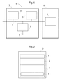
- the starting point of the present method is a virtual circuit model 1 in a suitable computer-based simulation environment.
- the circuit model 1 forms a logic circuit such as e.g.
- a system-on-chip or ASIC is implemented as a high-level model (e.g., ESL model) at the system level with a high-level programming language, such as e.g. Systems described.
- the virtual circuit model 1 in a first module 2 has three exemplary components 3 and in a second module 4, a component 3.
- These components 3 may be eg hardware components (eg electronic components, etc.) or system components (eg logic circuits, components with hardware and software components, etc.).
- a functional model also a high-level model in a programming language such eg systems.
- a functional behavior of the respective component 3 can be simulated. In this case, for example, 3 runtimes and / or services are specified as adjustable parameters for each component.
- the simulated data processing then takes place in accordance with these specifications with terms and performances that approximately correspond to the real logic circuit.
- the components 3 are interconnected with each other and with external (not shown) components through channels 5.
- a suitable bus is usually provided.
- Fig. 2 An extended with inventive attributes component 3 is in Fig. 2 shown.
- Component 3 is assigned defined security properties 6 (security properties).
- security properties 6 security properties
- known security concepts such as "confidentiality”, “integrity” (integrity), “authenticity” (authenticity) and “non-repudiation” are used, for example, in data processing.
- the security properties 6 for example, the degree of confidentiality and / or integrity and / or authenticity and / or traceability which the respective component 3 processes data is thus determined. With it finds a classification of each individual component 3 with regard to its security properties 6 for the protection of security-relevant data instead.
- defined security properties 6 determine with which degree of confidentiality and / or integrity and / or authenticity and / or traceability security-relevant data is transmitted through the respective channel 5.
- the determination of the security properties 6 takes place in such a way that in the simulation environment each component 3 and each channel 5 is linked with security parameters.
- the respective security parameter then defines e.g. as a number between 0 and 10, the degree of confidentiality and / or integrity and / or authenticity and / or traceability, etc. is determined.
- the component 3 For the processing of security-relevant data, the component 3 comprises suitable memory devices 7.
- defined security requirements 8 are defined for the security-relevant data. Specifically, these are stipulations as to what degree of confidentiality and / or integrity and / or authenticity and / or traceability is required. In this way, the security-relevant data to be processed by means of the component 3 or to be transmitted by means of a channel 5 are also classified.
- These security requirements 8 are also present in the simulation environment, e.g. by security parameters, which are linked to the data, determinable.
- security-relevant data is linked to a security status.
- This security status provides information as to whether the corresponding data is still trustworthy, for example, or whether there is a probability that a data manipulation has already taken place.
- Each component 3 of the circuit model 1 is expanded with a simulation unit 9. This first checks whether the security status and the security requirements 8 of the data processed in the respective component 3 corresponds to the security properties 6 of this component 3. For example, the data requires a high degree of confidentiality, which is why they have encryption as a security requirement 8. If such data is then processed or forwarded unencrypted, there is no correspondence between the security requirements 8 of the data and the security properties 6 of the affected component 3 or the affected channel 5. As a result of such non-correspondence, a security risk report is generated by means of the simulation unit 9 and forwarded to an output unit ,
- the modeling and application of an attack 10, 11, 12 takes place on a component 3 or a channel 5.
- the simulation unit 9 of a component 3 selects an attack 10, 11, 12 from a previously created library, shown in FIG Fig. 3 ,
- An attack 10, 11, 12 has various attack characteristics derived, for example, from the classifications "Confidentiality”, “Integrity”, “Authenticity” and “Detectability". For example, attack potential is set as an attack potential. Another marking concerns the type of attack, for example "key reconstruction”.
- an attack 10, 11, 12 is assigned an attack time trigger. The latter gives the simulation unit 9 of the respective component 3 when an attack is triggered ("armed"), whereby the Attack 10, 11, 12 depending on the configuration immediately or later.
- a triggered attack 10, 11, 12 interacts with the virtual circuit model 1.
- a respective attack 10, 11, 12 has access to data, whereby manipulation possibilities exist. Specifically, these manipulation options depend on which safety properties 6 the affected component 3 or the affected channel 5 has and which attack properties of the applied to this component 3 and this channel 5 attack 10, 11, 12 has.
- the library selects an attack 10 with Key Reconstructive properties as the attack type, High as the attack potential, and Immediately as the attack time trigger.
- these properties can be set in the simulation environment as attack parameters.
- this attack 10 Upon selection of this attack 10, it is immediately applied to an associated component 3. If this component has an encryption property with a strength level less than that of the attack potential (eg "medium"), then the attack 10 gains access to the data processed in this component 3 and can manipulate it. Accordingly, the security status of this data changes and an attack report with event data is generated and output to an output unit. There is the possibility to specify a probability for the attack success. In the security status of the data and in the attack report then appropriate probability data are given, eg that the data with a probability of 70% were manipulated.
- risk data can be derived from the probability data. For example, as a result of an attack simulation for each component 3 and each channel 5 a risk value (Security Risk Number) is issued. These risk values then provide information about how injury-prone components 3 and 5 are against the applied attacks 10-12.
- a comparison with a required level of risk shows immediately where the security measures have weak points or where unnecessary security measures have been taken. For example, by simulating a use case, it can be shown that execution of cryptographic functions is, to a lesser extent, sufficient than initially thought to protect the system.
- one or more attack graphs 14, 15 are formed, as in Fig. 4 shown.
- the execution of an attack graph 14 depends on the termination of another attack graph 15.
- the triggering of an attack graph 14, 15 applies a predetermined sequence of attacks 10, 11, 12 or 10, 13 to the circuit model 1.
- a mapping of an attack graph 14 to the circuit model 1 takes place, as in FIG Fig. 5 shown.
- This can be an attack 10-13 or multiple attacks 10-13 can be applied to one component 3 or to multiple components 3.
- attack graphs 14, 15 can be applied, whereby 10-13 security holes for the simulated application are shown by a suitable combination of attacks.
- a task can check a data packet by means of MAC control and request it again if necessary.
- the simulation unit 9 in the respective component 3 monitors the modeled circuit model 1 and reports security violations by means of corresponding reports via an output unit.
- data and data quality can be tracked and recorded during a simulation. This allows the tracking of security-relevant events.
- the effects of manipulated data on the circuit model 1 are determined.
- trusted data 16 are manipulated by attacks 10, 11.
- the circuit model 1 consists of four components 3, 3 ', 3 ", 3"', wherein a first component 3 is connected to a second component 3 'via a first bus and wherein the second component 3' via another bus with a third and a fourth component 3 ", 3"'is connected.
- a first attack 10 causes the reconstruction 17 of a key with which the first bus was previously protected.
- the data 16 routed through this channel 5 is decrypted.
- component 3 'already decrypted data 16' reach.
- This simulation action causes the security status associated with the data 16 'to change and a corresponding attack report 18 to be issued. It indicates, for example, that the data 16 routed through the named channel 5 'at a particular time was decrypted.
Abstract
Die Erfindung betrifft ein Verfahren zur Analyse einer logischen Schaltung, welche mehrere Komponenten (3, 3', 3", 3"') und Kanäle (5, 5') zum Austausch von Daten zwischen Komponenten (3, 3', 3", 3"') umfasst, wobei für eine Simulation einer Funktionsweise der logischen Schaltung jeder Komponente (3, 3', 3", 3"') und jedem Kanal (5, 5') in einem Schaltungsmodell (1) funktionale Eigenschaften zugeordnet werden. Dabei wird das Schaltungsmodell (1) in einem Verfahrensabschnitt in der Weise um Mechanismen zur Sicherheitsanalyse erweitert, dass der jeweiligen Komponente (3, 3', 3", 3"') und/oder dem jeweiligen Kanal (5, 5') zumindest eine definierte Sicherheitseigenschaft (6) zugeordnet wird und dass sicherheitsrelevante Daten (16, 16', 16") mit zumindest einer definierten Sicherheitsanforderung (8) und mit einem Sicherheitsstatus verknüpft werden. Zudem werden in einem weiteren Verfahrensabschnitt mittels einer Simulationseinheit (9) folgende Verfahrensschritte durchgeführt: Überprüfen, ob die Sicherheitseigenschaft (6) der jeweiligen Komponente (3, 3', 3", 3"') und/oder des jeweiligen Kanals (5, 5') der Sicherheitsanforderung (8) der sicherheitsrelevanten Daten (16, 16', 16") entspricht und bei Nichtentsprechung Generieren eines Sicherheitsrisikoberichts; Anwenden eines modellierten Angriffs (10, 11, 12, 13) auf eine Komponente (3, 3', 3", 3"') und/oder einen Kanal (5, 5'); Bestimmen einer Verletzbarkeit der Sicherheitseigenschaft (6) der jeweiligen Komponente (3, 3', 3", 3"') und/oder des jeweiligen Kanals (5, 5') durch den angewandten Angriff (10, 11, 12, 13) und bei gegebener Verletzbarkeit der Sicherheitseigenschaft (6) Generieren eines Angriffsberichts (18).The invention relates to a method for analyzing a logic circuit which has a plurality of components (3, 3 ', 3 ", 3"') and channels (5, 5 ') for exchanging data between components (3, 3', 3 ", 3 "'), wherein for a simulation of an operation of the logic circuit of each component (3, 3', 3", 3 "') and each channel (5, 5') in a circuit model (1) functional properties are assigned. In this case, the circuit model (1) is expanded in a method section in the manner to safety analysis mechanisms that the respective component (3, 3 ', 3 ", 3"') and / or the respective channel (5, 5 ') at least one security-related data (16, 16 ', 16 ") are associated with at least one defined security request (8) and with a security status Check whether the security property (6) of the respective component (3, 3 ', 3 ", 3"') and / or of the respective channel (5, 5 ') of the security requirement (8) of the security-relevant data (16, 16') , 16 ") and, if not met, generate a safety risk report; Applying a modeled attack (10, 11, 12, 13) to a component (3, 3 ', 3 ", 3"') and / or a channel (5, 5 '); Determining a vulnerability of the security property (6) of the respective component (3, 3 ', 3 ", 3"') and / or of the respective channel (5, 5 ') by the applied attack (10, 11, 12, 13) and given vulnerability of the security property (6) generate an attack report (18).
Description
Die vorliegende Erfindung betrifft allgemein das Gebiet der elektronischen logischen Schaltungen, insbesondere der integrierten Schaltungen wie z.B. der so genannten anwendungsspezifischen, integrierten Schaltungen oder ASICs, der so genannten Field Programmable Gate Arrays oder FPGAs und der so genannten System-on-Chip-Systeme. Im Speziellen bezieht sich die vorliegende Erfindung auf ein Verfahren zur Analyse einer logischen Schaltung, welche mehrere Komponenten und Kanäle zum Austausch von Daten zwischen Komponenten umfasst, wobei für eine Simulation einer Funktionsweise der logischen Schaltung jeder Komponente und jedem Kanal in einem Schaltungsmodell funktionale Eigenschaften zugeordnet werden.The present invention relates generally to the field of electronic logic circuits, in particular integrated circuits, e.g. the so-called application-specific, integrated circuits or ASICs, the so-called field programmable gate arrays or FPGAs and the so-called system-on-chip systems. More particularly, the present invention relates to a method of analyzing a logic circuit that includes a plurality of components and channels for exchanging data between components, wherein functional characteristics are assigned to simulate operation of the logic circuit of each component and each channel in a circuit model ,
Logische Schaltungen werden in zahlreichen elektrischen und elektronischen Geräten bzw. Systemen eingesetzt. Solche Schaltungen umfassen in der Regel ein Substrat (z.B. einem Halbleitersubstrat), auf dem unterschiedliche Bauelemente oder Bauelementblöcke untergebracht und miteinander verdrahtet sind. Diese Bauelemente bzw. Bauelementblöcke werden auch als Komponenten bezeichnet. Eine integrierte Schaltung besteht üblicherweise aus einer Anzahl verschiedener Komponenten, welche auf einem einkristallinen Substrat untergebracht sind. Sind alle oder ein großer Teil der gewünschten Funktionen auf einem Chip verwirklicht, spricht man von einem System-on-Chip. Mittels dieser Integration stehen umfangreiche Funktionalitäten und Anwendungen auf kleinstem Raum zur Verfügung. Durch den raschen Fortschritt in der technologischen Entwicklung besteht heute die Möglichkeit, komplexe logische Schaltungen mit einer großen Anzahl an Komponenten auf einem einzigen Halbleiter-Chip unterzubringen.Logical circuits are used in numerous electrical and electronic devices or systems. Such circuits typically include a substrate (eg, a semiconductor substrate) on which different devices or device blocks are housed and wired together. These components or component blocks are also referred to as components. An integrated circuit usually consists of a number of different components which are accommodated on a monocrystalline substrate. If all or a large part of the desired functions are realized on a chip, this is called a system-on-chip. This integration provides extensive functionality and applications in the smallest of spaces. With the rapid advances in technological development, it is now possible to package complex logic circuits with a large number of components on a single semiconductor chip.
Entworfen werden solche komplexen Schaltungen üblicherweise mittels rechnergestützter Hilfsmittel. Dabei erfolgt zunächst die Erstellung eines virtuellen Schaltungsmodells, um eine gewünschte Funktionsweise zu simulieren. Konkret wird jede Komponente (Hardwarekomponenten; Systemkomponenten, welche aus Hardware- und Softwareanteilen bestehen, etc.) durch ein funktionales Komponentenmodell dargestellt, um daraus ein Schaltungsmodell der logischen Schaltung bzw. des logischen Systems aufzubauen. Anhand dieses Schaltungsmodells ist mittels Simulation eine Funktionalität der entsprechenden Schaltung überprüfbar und verifizierbar. Das gilt insbesondere für ein Schaltungsmodell mit hohem Abstraktionsgrad, welches auch als High-Level-Modell bezeichnet wird. Unter Verwendung einer sogenannten High-Level-Programmiersprache wie C++, Systeme, System-Verilog, etc. können zum Beispiel die funktionalen Komponentenmodelle und Schaltungsmodelle logischer Schaltungen abgefasst, dargestellt und ein funktionales Verhalten der logischen Schaltung sowie der einzelnen Komponenten der logischen Schaltung simuliert werden. Konkret werden dabei z.B. Laufzeiten und/oder Leistungen der einzelnen Funktionskomponenten als Parameter festgelegt, damit sich das Schaltungsmodell während einer Simulation so verhält wie die entsprechende reale Schaltung bzw. ein reales Hardwaremodell.Such complex circuits are usually designed by means of computer-aided tools. At first, a virtual circuit model is created in order to simulate a desired mode of operation. Specifically, each component (hardware components, system components consisting of hardware and software parts, etc.) is represented by a functional component model to construct a circuit model of the logical circuit and the logical system, respectively. On the basis of this circuit model, a functionality of the corresponding circuit can be checked and verified by means of simulation. This applies in particular to a circuit model with a high degree of abstraction, which is also referred to as a high-level model. Using a so-called high-level programming language such as C ++, systems, system verilog, etc., for example, the functional component models and circuit models of logical circuits can be drafted, presented and a functional behavior of the logic circuit and the individual components of the logic circuit can be simulated. Specifically, e.g. Maturities and / or powers of the individual function components are set as parameters, so that the circuit model behaves during a simulation as the corresponding real circuit or a real hardware model.
Ein wichtiges Ziel bei der Entwicklung von komplexen Schaltungen (Systemen) ist die Absicherung gegen Angriffe (Security-Attacken). Um diese zu erschweren bzw. zu vermeiden werden Sicherheitsmaßnahmen in das Design der Schaltung integriert. Damit sollen im System abgespeicherte bzw. verarbeitete sicherheitsrelevante Daten geschützt werden. Um diese Sicherheitsmaßnahmen zu bestimmen und optimal auszulegen, ist eine Analyse des Designs erforderlich. Dabei wird untersucht, welche Komponenten des Systems explizit oder implizit durch Angriffe betroffen sein können und welche Sicherheitsmaßnahmen in welchem Ausmaß für einen jeweiligen Anwendungsfall sinnvoll sind.An important goal in the development of complex circuits (systems) is the protection against attacks (security attacks). To complicate or avoid this, security measures are integrated into the design of the circuit. This should protect the system stored or processed security-related data. Determining and optimizing these security measures requires an analysis of the design. It is examined which components of the system can be affected explicitly or implicitly by attacks and which security measures are appropriate and to what extent for a particular application.
Üblicherweise geschieht eine derartige Analyse anhand fortlaufender Inspektionen und Reviews des Systems durch einen Entwickler (Architekten) während eines Entwicklungsprozesses. Bekannt ist auch die Anwendung einer sogenannten Attack-Tree-Analyse.Typically, such an analysis is done by ongoing inspections and reviews of the system by a developer (architect) during a development process. Also known is the application of a so-called attack-tree analysis.
Aufgrund der zunehmenden Größe und Komplexität logischer Schaltungen wird es zunehmend schwierig, die Auswirkungen möglicher Angriffe auf die Funktionalität und die Sicherheit umfassend zu untersuchen.With the increasing size and complexity of logic circuits, it becomes increasingly difficult to fully investigate the effects of potential attacks on functionality and security.
Der Erfindung liegt die Aufgabe zugrunde, das eingangs genannte Verfahren weiterzubilden, um eine verlässliche Sicherheitsanalyse durchzuführen zu können.The invention has the object of developing the aforementioned method in order to perform a reliable safety analysis.
Gelöst wird diese Aufgabe mittels eines Verfahrens gemäß Anspruch 1. Vorteilhafte Ausgestaltungen und Weiterbildungen der Erfindung sind Gegenstand der abhängigen Ansprüche.This object is achieved by means of a method according to claim 1. Advantageous embodiments and further developments of the invention are the subject of the dependent claims.
Dabei wird das Schaltungsmodell in einem Verfahrensabschnitt in der Weise um Mechanismen zur Sicherheitsanalyse erweitert, dass der jeweiligen Komponente und/oder dem jeweiligen Kanal zumindest eine definierte Sicherheitseigenschaft zugeordnet wird und dass sicherheitsrelevante Daten mit zumindest einer definierten Sicherheitsanforderung und mit einem Sicherheitsstatus verknüpft werden, und dass in einem weiteren Verfahrensabschnitt mittels einer Simulationseinheit folgende Verfahrensschritte durchgeführt werden:
- Überprüfen, ob die Sicherheitseigenschaft der jeweiligen Komponente und/oder des jeweiligen Kanals der Sicherheitsanforderung der sicherheitsrelevanten Daten entspricht und bei Nichtentsprechung Generieren eines Sicherheitsrisikoberichts,
- Anwenden eines modellierten Angriffs auf eine Komponente und/oder einen Kanal,
- Bestimmen einer Verletzbarkeit der Sicherheitseigenschaft der Komponente und/oder des Kanals durch den angewandten Angriff und bei gegebener Verletzbarkeit der Sicherheitseigenschaft Generieren eines Angriffsberichts.
- Checking whether the security property of the respective component and / or the respective channel corresponds to the security requirement of the security-relevant data and, in the case of non-compliance, generating a security risk report;
- Applying a modeled attack on a component and / or a channel,
- Determining a vulnerability of the security property of the component and / or the channel by the applied attack and given vulnerability of the security property generating an attack report.
Somit erfolgt bereits im Designstadium anhand einer Simulation eine Sicherheitsanalyse mit Berichten hinsichtlich der Eignung der eingestellten Sicherheitseigenschaften und hinsichtlich der Verletzbarkeit durch einen virtuell ausgeführten Angriff. Erfolgt beispielsweise eine Manipulation von Daten in einer angegriffenen Komponente, wandern diese manipulierten Daten entsprechend der Funktionalität des Schaltungsmodells durch weitere Komponenten. Auch bei diesen Komponenten wird die Verletzbarkeit der Sicherheitseigenschaften infolge einer Verarbeitung der manipulierten Daten bestimmt. Gegebenenfalls können anschließend zur Optimierung des Systems zusätzliche Sicherheitsmaßnahmen eingefügt oder entfernt werden.Thus, already at the design stage, a simulation is used to perform a safety analysis with reports on the suitability of the set safety properties and on the vulnerability of a virtually executed attack. For example, if a manipulation of data in an attacked component, this manipulated data migrate through other components according to the functionality of the circuit model. Also with these components, the vulnerability of the security properties is determined as a result of processing the manipulated data. If necessary, additional security measures can subsequently be inserted or removed to optimize the system.
Damit ist sichergestellt, dass alle Folgewirkungen von manipulierten Daten erkannt werden und die logische Schaltung ausreichend robust gegenüber allen modellierten und angewendeten Angriffen ist.This ensures that all consequential effects of manipulated data are detected and the logic circuitry is sufficiently robust against all modeled and applied attacks.
Mit diesem Verfahren sind auch solche Angriffe überprüfbar, deren Simulationen üblicherweise sehr viel Zeit in Anspruch nehmen, wie beispielsweise die Rekonstruktion kryptographischer Verschlüsselungsalgorithmen. Im vorliegenden Verfahren muss lediglich bestimmt werden, ob der modellierte Angriff ein ausrechendes Potenzial aufweist, um eine definierte Sicherheitseigeneschaft der angegriffenen Komponente zu überwinden. Wenn das der Fall ist, erfolgt eine Bestätigung einer gegebenen Verletzbarkeit mittels eines generierten Angriffsberichts.With this method, such attacks are also verifiable, whose simulations usually take a great deal of time, such as the reconstruction of cryptographic encryption algorithms. In the present method, it only needs to be determined if the modeled attack has sufficient potential to overcome a defined security property of the attacked component. If so, a given vulnerability is confirmed by a generated attack report.
Zudem werden mittels Simulationseinheit schon in der Designphase des Schaltungsmodells Abweichungen zwischen den Sicherheitsanforderungen der Daten und den Sicherheitseigenschaften der Komponenten erkannt und gemeldet.In addition, deviations between the. Are already created in the design phase of the circuit model by means of the simulation unit Security requirements of the data and the security properties of the components detected and reported.
Von Vorteil ist es, wenn jede Komponente und jeder Kanal mit einer eigenen Simulationseinheit erweitert wird. Diese führt dann während einer Simulation für den jeweiligen Kanal bzw. die jeweilige Komponente die Überprüfungsschritte durch und generiert bei erkannten Sicherheitsrisiken einen entsprechenden Bericht.It is advantageous if each component and each channel is expanded with its own simulation unit. The latter then carries out the checking steps during a simulation for the respective channel or the respective component and generates a corresponding report if security risks are detected.
Dabei ist es sinnvoll, wenn als Resultat eines angewandten Angriffs Ereignisdaten generiert werden. Diese Ereignisdaten beschreiben eine gegebenenfalls erfolgte Manipulation von Daten, wodurch eine genauere Analyse ermöglicht wird.It makes sense to generate event data as a result of an applied attack. This event data describes any manipulation of data that may be possible, allowing more accurate analysis.
In einer weiteren vorteilhaften Ausprägung der Erfindung werden zur Bestimmung der Verletzbarkeit der jeweiligen Sicherheitseigenschaft Wahrscheinlichkeitsdaten generiert. Im Angriffsbericht ist dann angegeben, mit welcher Wahrscheinlichkeit der Angriff erfolgreich ist. Zudem können die Wahrscheinlichkeitsdaten Auskunft darüber geben, wie lange der Angriff voraussichtlich dauert, bis die betroffene Sicherheitseigenschaft verletzt wird.In a further advantageous embodiment of the invention, probability data are generated to determine the vulnerability of the respective security property. The attack report then indicates what probability the attack is successful with. In addition, the probability data may indicate how long the attack is likely to take until the security property concerned is violated.
In weiterer Folge werden sinnvollerweise aus den Wahrscheinlichkeitsdaten Risikodaten zur Bewertung der jeweiligen Sicherheitseigenschaft abgeleitet. Anhand dieser Risikodaten ist auf einfache Weise feststellbar, ob eine Sicherheitseigeneschaft ergänzt werden muss oder vermindert werden kann. Ist zum Beispiel für die zu entwickelnde Schaltung ein tolerierbares Risikoniveau festgelegt, erfolgt zunächst ein Abgleich der Risikodaten mit diesem Risikoniveau. Übersteigt bei einer Komponente das ermittelte Risiko die Vorgabe, muss die Sicherheitseigenschaft ergänzt werden. Im umgekehrten Fall wird damit auch eine überzogene Sicherheitseigeneschaft erkannt.Subsequently, it is useful to derive risk data for evaluating the respective security property from the probability data. On the basis of this risk data, it can be easily determined whether a security property has to be supplemented or reduced. If, for example, a tolerable risk level is defined for the circuit to be developed, the risk data is initially compared with this level of risk. For a component, if the identified risk exceeds the target, the safety feature must be supplemented. In the opposite case, this also detects an excessive security property.
Eine einfache Weiterbildung der Erfindung sieht vor, dass ein Angriff aus einer zuvor erstellten Bibliothek ausgewählt wird. Damit muss nicht für jeden Anwendungsfall erneut ein Angriff erstellt werden. Vielmehr erfolgt das Modellieren eines Angriffs durch einfache Auswahl aus der Bibliothek und gegebenenfalls durch Anpassungen von Angriffsparametern.A simple development of the invention provides that an attack is selected from a previously created library. This eliminates the need to re-create an attack for each use case. Rather, an attack is modeled by simply selecting it from the library and, if necessary, adjusting attack parameters.
Dabei ist es von Vorteil, wenn jedem Angriff ein Angriffspotenzial und/oder ein Angriffstyp und/oder ein Angriffszeittrigger zugeordnet werden/wird. Anhand dieser Attribute ist ein Angriff in einfacher Weise auswählbar bzw. in geänderter Ausprägung modellierbar.It is advantageous if each attack is / will be assigned an attack potential and / or an attack type and / or an attack time trigger. On the basis of these attributes, an attack can be selected in a simple manner or can be modeled in a modified form.
Um die Effizienz des vorliegenden Verfahrens weiter zu erhöhen, ist in einer Weitereinwicklung vorgesehen, dass ein Angriffsgraph mit mehreren Graphenknoten modelliert wird und dass jeder Graphenknoten einem Angriff entspricht, welcher auf eine bestimmte Komponente und/oder einen bestimmten Kanal angewendet wird. Damit kommen weitere Verfahrensschritte hinzu, in denen zusätzliche Angriffe entsprechend dem modellierten Angriffsgraphen auf einzelne Komponenten bzw. Kanäle angewandt werden und wobei wiederum eine Bestimmung der Verletzbarkeit der jeweiligen Sicherheitseigenschaften der betroffenen Komponenten erfolgt. Aus den festgestellten Auswirkungen der multiplen Angriffe sind die notwendigen Schritte zur Anpassung der Sicherheitsmaßnahmen ableitbar.To further increase the efficiency of the present method, it is contemplated in a further development that an attack graph is modeled with multiple graph nodes and that each graph node corresponds to an attack applied to a particular component and / or channel. This adds further method steps in which additional attacks are applied to individual components or channels in accordance with the modeled attack graph, and in turn a determination of the vulnerability of the respective security properties of the affected components takes place. From the observed effects of the multiple attacks, the necessary steps for adapting the security measures can be derived.
Von Vorteil ist in weiterer Folge, wenn mehrere Angriffsgraphen miteinander verknüpft werden, sodass ein Angriffsgraph in Abhängigkeit eines Ausführungsfortschrittes eines anderen Angriffsgraphen ausgeführt wird. Damit wird die Komplexität der anwendbaren Angriffsszenarien weiter gesteigert. Mit dieser zunehmenden Komplexität steigt auch die erzielbare Sicherheit der zu entwickelten Schaltung gegenüber jeglicher Form von Angriffen.Another advantage is that when multiple attack graphs are linked together, so that an attack graph is executed in response to an execution progress of another attack graph. This further increases the complexity of the applicable attack scenarios. With this increasing complexity, the achievable security of the developed circuit also increases against any form of attack.
Für das Schaltungsmodell der logischen Schaltung ist günstigerweise vorgesehen, dass dieses als High-Level-Modell, insbesondere als so genanntes Electronic-System-Level-Modell, ausgeführt wird. Während verschiedener Schritte eines Design-Prozesses für eine logische Schaltung, insbesondere für ASICs, werden unterschiedliche Schaltungsmodelle mit unterschiedlichem Abstraktionsgrad kreiert. Mit diesen Schaltungsmodellen können auch unterschiedliche Funktionalitäten der logischen Schaltung getestet werden. Am Beginn eines Design-Prozesses wird ein so genanntes High-Level-Modell oder insbesondere ein so genanntes Electronic-System-Level- oder ESL-Modell, der logischen Schaltung entworfen. Mit diesem Modell können einerseits auf einfache Weise Funktionalitäten, Algorithmen, etc. der einzelnen Komponenten sowie der logischen Schaltung modelliert bzw. funktionale Modelle von Komponenten und Schaltung kreiert werden und andererseits sind die Auswirkungen von Angriffen und die Verletzbarkeit der eingestellten Sicherheitseigenschaften effizient überprüfbar.For the circuit model of the logic circuit is advantageously provided that this is designed as a high-level model, in particular as a so-called electronic system-level model. During various steps of a logic circuit design process, particularly for ASICs, different circuit models are created with different degrees of abstraction. With these circuit models also different functionalities of the logic circuit can be tested. At the beginning of a design process, a so-called high-level model or in particular a so-called electronic system level or ESL model, the logical circuit is designed. With this model on the one hand functionalities, algorithms, etc. of the individual components as well as the logical circuit can be modeled respectively functional models of components and circuit can be created and on the other hand the effects of attacks and the vulnerability of the set security properties can be checked efficiently.
Zudem ist es günstig, wenn als logische Schaltung eine integrierte Schaltung, insbesondere eine so genannte anwendungsspezifische, integrierte Schaltung oder ein so genanntes System-on-Chip, vorgesehen wird. Eine integrierte Schaltung kann aus einer Kombination von mehreren elektrisch verbundenen elektronischen Komponenten - meist Halbleiterbauelementen (z.B. Dioden, Transistoren, etc.) und/oder weiteren aktiven wie passiven Bauelementen (z.B. Widerständen, etc.) bestehen. Anwendungen finden integrierte Schaltungen in vielen Bereichen mit hohen Sicherheitsanforderungen, beispielsweise beim Aufbau von Prozessoren, Controllern, Datenspeichern, etc.In addition, it is favorable if an integrated circuit, in particular a so-called application-specific integrated circuit or a so-called system-on-chip, is provided as the logic circuit. An integrated circuit may consist of a combination of several electrically connected electronic components - mostly semiconductor devices (e.g., diodes, transistors, etc.) and / or other active and passive devices (e.g., resistors, etc.). Applications find integrated circuits in many areas with high security requirements, such as the construction of processors, controllers, data storage, etc.
Eine spezielle Form integrierter Schaltungen sind die so genannten anwendungsspezifischen, integrierten Schaltungen (ASICs), welche heutzutage in vielen verschiedenen elektronischen Geräten zum Einsatz kommen. Bei einem ASIC wird eine Funktionalität der logischen Schaltung bereits bei der Entwicklung und Herstellung eindeutig festgelegt und ist danach nicht mehr veränderbar. Das bedeutet, ein ASIC weist eine strikte Abhängigkeit von den zu verarbeiteten Daten auf und die in einem ASIC implementierte Logik steht in engem Zusammenhang mit der oder den auszuführenden Funktionen. Daher ist es bei ASICs besonders wichtig, dass auf einfache und kostengünstige Weise bereits in der Design- oder Entwicklungsphase eine Systemsicherheit ermittelt und geprüft wird, ob beispielsweise geforderte oder gewünschte Risikovorgaben eingehalten werden.A special form of integrated circuits are the so-called application specific integrated circuits (ASICs), which are used today in many different electronic devices. At an ASIC For example, a functionality of the logic circuit is already clearly defined during development and production and can not be changed afterwards. That is, an ASIC has a strict dependency on the data being processed, and the logic implemented in an ASIC is closely related to the one or more functions to be performed. Therefore, it is particularly important for ASICs that system security is determined and checked in a simple and cost-effective manner already during the design or development phase, for example, whether the required or desired risk specifications are met, for example.
Eine weitere Form einer integrierten Schaltung ist das sogenannte System-on-Chip oder Ein-Chip-System. Dabei erfolgt eine Integration aller oder eines großen Teils der Funktionen eines Systems (z.B. embedded Computer, etc.). Als System wird eine Kombination von unterschiedlichen Komponenten wie z.B. logischen Schaltungen, Taktgebung, mikrotechnische Sensoren, Speichereinheiten, Prozessoren, Schnittstellen, Bussystem, etc.) aufgefasst, von welchen zusammen eine bestimmte Funktionalität bereitgestellt wird. Für derartige Ausprägungen ist das Verfahren besonders geeignet, weil hier mit herkömmlichen Methoden aufgrund der zunehmenden Systemgröße und -komplexität nur mehr unzureichende Bewertungen der Sicherheitssituation möglich sind.Another form of integrated circuit is the so-called system-on-chip or one-chip system. Thereby an integration of all or a large part of the functions of a system (for example embedded computer, etc.) takes place. As a system, a combination of different components, e.g. logical circuits, timing, microtechnical sensors, memory units, processors, interfaces, bus system, etc.), of which together a certain functionality is provided. For such characteristics, the method is particularly suitable, because here only more inadequate assessments of the security situation are possible with conventional methods due to the increasing system size and complexity.
Eine weitere günstige Verbesserung sieht vor, dass als logische Schaltung eine so genannte Feld-programmierbare Logikgatter-Anordnung oder ein so genanntes Field Programmable Gate Array vorgesehen wird. Mittels derartiger Feld-programmierbaren Logikgatter-Anordnungen oder FPGAs können durch eine spezifische Konfiguration interner Strukturen (z.B. Gatter, logischer Blöcke, etc.) verschiedene Schaltungen - von einfachen Schaltungen wie z.B. einer Zählerschaltung bis zu hochkomplexen Schaltungen wie z.B. einem Mikroprozessor - realisiert werden. FPGAs werden in allen Bereichen der Digitaltechnik eingesetzt, insbesondere in Bereichen, wo es auf schnelle Signalverarbeitung und eine flexible Änderbarkeit der Schaltung ankommt. Im Vergleich mit anderen logischen Schaltungen, insbesondere ASICs, weisen FPGAs den Vorteil von geringeren Entwicklungskosten und sehr kurzen Implementierungszeiten auf. Ein besondere Vorteil von FPGAs ist, dass sie umkonfigurierbar sind und damit eine mit einem FPGA realisierte logische Schaltung einfach korrigierbar und - falls notwendig - mit Sicherheitsmechanismen erweiterbar ist.Another favorable improvement provides that a so-called field-programmable logic gate arrangement or a so-called Field Programmable Gate Array is provided as the logic circuit. By means of such field programmable logic gate arrays or FPGAs, various circuits can be realized by a specific configuration of internal structures (eg, gates, logic blocks, etc.) - from simple circuits such as a counter circuit to highly complex circuits such as a microprocessor. FPGAs are used in all areas of digital technology, in particular in areas where fast signal processing and flexible changeability of the circuit are important. In comparison with other logic circuits, in particular ASICs, FPGAs have the advantage of lower development costs and very short implementation times. A particular advantage of FPGAs is that they can be reconfigured, so that a logic circuit realized with an FPGA can easily be corrected and, if necessary, can be expanded with security mechanisms.
Die Erfindung wird nachfolgend in beispielhafter Weise unter Bezugnahme auf die beigefügten Figuren erläutert. Es zeigen in schematischer Darstellung:
- Fig. 1
- Virtuelles Schaltungsmodell einer logischen Schaltung
- Fig. 2
- Erweiterung einer Komponente bzw. eines Kanals
- Fig. 3
- Bibliothek mit verschiedenen Angriffen
- Fig. 4
- verschiedene Angriffsgraphen
- Fig. 5
- Angriffsgraph mit Angriffen auf unterschiedliche Komponenten eines Schaltungsmodells
- Fig. 6
- Angriffsgraph mit Angriffen auf unterschiedliche Komponenten eines Schaltungsmodells und Verarbeitung sicherheitsrelevanter Daten
- Fig. 1
- Virtual circuit model of a logic circuit
- Fig. 2
- Extension of a component or a channel
- Fig. 3
- Library with various attacks
- Fig. 4
- different attack graphs
- Fig. 5
- Attack graph with attacks on different components of a circuit model
- Fig. 6
- Attack graph attacking different components of a circuit model and processing security-related data
Ausgangspunkt des vorliegenden Verfahrens ist ein virtuelles Schaltungsmodell 1 in einer geeigneten rechnerbasierten Simulationsumgebung. Das Schaltungsmodell 1 bildet eine logische Schaltung wie z.B. ein System-on-Chip oder ASIC ab und wird beispielsweise in einer Design- oder Entwicklungsphase als High-Level-Modell (z.B. ESL-Modell) auf System-Level mit einer high-level Programmiersprache wie z.B. Systeme beschrieben.The starting point of the present method is a virtual circuit model 1 in a suitable computer-based simulation environment. The circuit model 1 forms a logic circuit such as e.g. For example, in a design or development phase, a system-on-chip or ASIC is implemented as a high-level model (e.g., ESL model) at the system level with a high-level programming language, such as e.g. Systems described.
Im Beispiel gemäß
Verbunden sind die Komponenten 3 untereinander und mit externen (nicht dargestellten) Komponenten durch Kanäle 5. Dafür ist in der Regel ein geeigneter Bus vorgesehen.The
Eine mit erfindungsgemäßen Attributen erweiterte Komponente 3 ist in
Mit den Sicherheitseigenschaften 6 wird also beispielsweise festgelegt, mit welchem Grad an Vertraulichkeit und/oder Integrität und/oder Authentizität und/oder Nachweisbarkeit die jeweilige Komponente 3 Daten verarbeitet. Damit findet eine Klassifizierung jeder einzelnen Komponente 3 hinsichtlich ihrer Sicherheitseigenschaften 6 zum Schutz sicherheitsrelevanter Daten statt.With the
Dasselbe gilt für einen Kanal 5. Auch hier wird mit definierten Sicherheitseigenschaften 6 festgelegt, mit welchem Grad an Vertraulichkeit und/oder Integrität und/oder Authentizität und/oder Nachweisbarkeit sicherheitsrelevante Daten durch den jeweiligen Kanal 5 übertragen werden.The same applies to a
Zum Beispiel erfolgt die Festlegung der Sicherheitseigenschaften 6 in der Weise, dass in der Simulationsumgebung jede Komponente 3 und jeder Kanal 5 mit Sicherheitsparametern verknüpft wird. Der jeweilige Sicherheitsparameter legt dann z.B. als eine Zahl zwischen 0 und 10 fest, wie hoch der Grad an Vertraulichkeit und/oder Integrität und/oder Authentizität und/oder Nachweisbarkeit etc. ist.For example, the determination of the
Zur Verarbeitung von sicherheitsrelevanten Daten umfasst die Komponente 3 geeignete Speichereinrichtungen 7. Dabei sind für die sicherheitsrelevanten Daten definierte Sicherheitsanforderungen 8 festgelegt. Konkret handelt es sich um Festlegungen, welcher Grad an Vertraulichkeit und/oder Integrität und/oder Authentizität und/oder Nachweisbarkeit gefordert ist. Auf diese Weise sind auch die mittels der Komponente 3 zu verarbeitenden bzw. mittels eines Kanals 5 zu übertragenden sicherheitsrelevanten Daten klassifiziert. Auch diese Sicherheitsanforderungen 8 sind in der Simulationsumgebung z.B. durch Sicherheitsparameter, welche mit den Daten verknüpft werden, festlegbar.For the processing of security-relevant data, the
Zudem sind alle sicherheitsrelevanten Daten mit einem Sicherheitsstatus verknüpft. Dieser Sicherheitsstatus gibt Auskunft darüber, ob die entsprechenden Daten z.B. noch vertrauenswürdig sind ob eine Wahrscheinlichkeit besteht, dass bereits eine Datenmanipulation stattgefunden hat.In addition, all security-relevant data is linked to a security status. This security status provides information as to whether the corresponding data is still trustworthy, for example, or whether there is a probability that a data manipulation has already taken place.
Jede Komponente 3 des Schaltungsmodells 1 ist mit einer Simulationseinheit 9 erweitert. Diese überprüft zunächst, ob der Sicherheitsstatus und die Sicherheitsanforderungen 8 der Daten, die in der jeweiligen Komponente 3 verarbeitet werden, den Sicherheitseigenschaften 6 dieser Komponente 3 entspricht. Beispielweise erfordern die Daten einen hohen Grad an Vertraulichkeit, weshalb diese eine Verschlüsselung als Sicherheitsanforderung 8 aufweisen. Werden solche Daten dann unverschlüsselt verarbeitet oder weitergeleitet, herrscht keine Übereinstimmung zwischen den Sicherheitsanforderungen 8 der Daten und den Sicherheitseigeneschaften 6 der betroffenen Komponente 3 oder des betroffenen Kanals 5. Als Resultat einer solchen Nichtentsprechung wird mittels der Simulationseinheit 9 ein Sicherheitsrisikobericht generiert und an eine Ausgabeeinheit geleitet.Each
In einem weiteren Verfahrensschritt erfolgt die Modellierung und Anwendung eines Angriffs 10, 11, 12 auf eine Komponente 3 oder einen Kanal 5. Dabei wählt beispielsweise die Simulationseinheit 9 einer Komponente 3 einen Angriff 10, 11, 12 aus einer zuvor erstellten Bibliothek, dargestellt in
Ein Angriff 10, 11, 12 weist verschiedene Angriffseigenschaften auf, welche beispielsweise von den Klassifizierungen "Vertraulichkeit", "Integrität", "Authentizität" und "Nachweisbarkeit" abgeleitet sind. Zum Beispiel wird als ein Angriffspotenzial die Angriffsstärke festgelegt. Eine weitere Kennzeichnung betrifft den Angriffstyp, beispielsweise "Schlüsselrekonstruktion". Zur Festlegung eines Angriffszeitpunktes wird einem Angriff 10, 11, 12 ein Angriffszeittrigger zugeordnet. Letzterer gibt der Simulationseinheit 9 der jeweiligen Komponente 3 vor, wann ein Angriff ausgelöst ("scharf geschaltet") wird, wodurch der Angriff 10, 11, 12 je nach Konfiguration sofort oder erst später erfolgt.An
Das Wesen der vorliegenden Erfindung liegt darin, dass während einer Simulation ein ausgelöster Angriff 10, 11, 12 mit dem virtuellen Schaltungsmodell 1 interagiert. Ein jeweiliger Angriff 10, 11, 12 hat dabei Zugriff auf Daten, wobei Manipulationsmöglichkeiten bestehen. Konkret hängen diese Manipulationsmöglichkeiten davon ab, welche Sicherheitseigenschaften 6 die betroffenen Komponente 3 oder der betroffene Kanal 5 aufweist und welche Angriffseigenschaften der auf diese Komponente 3 bzw. diesen Kanal 5 angewendete Angriff 10, 11, 12 aufweist.The essence of the present invention is that during a simulation, a
Beispielsweise wird aus der Bibliothek ein Angriff 10 mit Eigenschaften "Schlüsselrekonstruktion" als Angriffstyp, "hoch" als Angriffspotenzial und "sofort" als Angriffszeittrigger ausgewählt. Diese Eigenschaften sind in der Simulationsumgebung beispielsweise als Angriffsparameter einstellbar.For example, the library selects an
Nach Auswahl dieses Angriffs 10 wird dieser sofort auf eine zugeordnete Komponente 3 angewendet. Weist diese Komponente eine Verschlüsselungseigenschaft auf, deren Stärkegrad geringer als jener des Angriffspotenzials ist (z.B. "mittel"), dann erhält der Angriff 10 Zugriff auf die in dieser Komponente 3 verarbeiteten Daten und kann diese manipulieren. Dementsprechend ändert sich der Sicherheitsstatus dieser Daten und ein Angriffsbericht mit Ereignisdaten wird generiert und an eine Ausgabeeinheit ausgegeben. Dabei besteht die Möglichkeit, eine Wahrscheinlichkeit für den Angriffserfolg anzugeben. Im Sicherheitsstatus der Daten und im Angriffsbericht sind dann entsprechende Wahrscheinlichkeitsdaten angegeben, z.B. dass die Daten mit einer Wahrscheinlichkeit von 70% manipuliert wurden.Upon selection of this
Zudem werden als Ereignisdaten im Angriffsbericht eine Kennung des entsprechenden Angriffs, eine Kennung der betroffenen Komponente und ein Zeitpunkt bzw. eine Zeitdauer der Angriffsdurchführung etc. ausgegeben. Es besteht auch die Möglichkeit, für verschiedene Zeitdauern unterschiedliche Wahrscheinlichkeitsdaten zu berechnen. Dabei wird z.B. anhand der Sicherheitsparameter der Komponente 3, der Daten und des Angriffs 10 berechnet, wie lange der Angriff 10 dauern müsste, damit es mit einer bestimmten Wahrscheinlichkeit zu einer Verletzung kommt. In weiterer Folge können aus den Wahrscheinlichkeitsdaten Risikodaten abgeleitet werden. Beispielsweise wird als Resultat einer Angriffssimulation für jede Komponente 3 und jeden Kanal 5 ein Risikowert (Security Risk Number) ausgegeben. Diese Risikowerte geben dann Auskunft darüber, wie verletzungsanfällige die Komponenten 3 und Kanäle 5 gegenüber den angewendeten Angriffen 10-12 sind. Ein Vergleich mit einem geforderten Risikoniveau zeigt dann sofort, wo die Sicherheitsmaßnahmen Schwachstellen aufweisen oder wo gegebenenfalls unnötige Sicherheitsmaßnahmen gesetzt wurden. Zum Beispiel kann durch die Simulation eines Anwendungsfalls gezeigt werden, dass die Ausführung kryptographischer Funktionen in niedrigerem Ausmaß ausreichend ist als anfänglich vermutet, um das System zu schützen.In addition, as the event data in the attack report, an identifier of the corresponding attack, an identifier of the affected component and a time or duration of the attack execution, etc. issued. It is also possible to calculate different probability data for different periods of time. In doing so, e.g. Based on the
In einer Weiterbildung der Erfindung können durch Auswahl und Kombination von Angriffen 10, 11, 12, 13 ein oder mehrere Angriffsgraphen 14, 15 gebildet werden, wie in
Konkret findet während einer Simulation ein Mapping eines Angriffsgraphen 14 auf das Schaltungsmodell 1 statt, wie in
Auf diese Weise ist die Möglichkeit geschaffen, verschiedene Anwendungsfälle (Use Cases) auf das virtuelle Schaltungsmodell 1 anzuwenden. Solche Anwendungsfälle können z.B. mit der sogenannten Task-Graph Methode (Platform Architect der Fa. Synopsys) erstellt werden.In this way, the possibility is created to apply different use cases (use cases) to the virtual circuit model 1. Such applications may e.g. be created with the so-called Task-Graph method (Platform Architect Synopsys).
Bei der Simulation und Analyse des Schaltungsmodells können verschiedene Angriffsgraphen 14, 15 angewendet werden, wobei durch passende Kombination von Angriffen 10-13 Sicherheitslücken für den simulierten Anwendungsfall aufgezeigt wird. Beispielsweise kann bei einem Angriff 10 ein Task mittels MAC Kontrolle ein Datenpaket prüfen und im Bedarfsfall neu anfordern.In the simulation and analysis of the circuit model,
Die Simulationseinheit 9 in der jeweiligen Komponente 3 überwacht das modellierte Schaltungsmodell 1 und meldet Sicherheitsverletzungen mittels entsprechender Berichte über eine Ausgabeeinheit. Somit können Daten und Datenqualität während einer Simulation verfolgt und aufgezeichnet werden. Das erlaubt die Rückverfolgung sicherheitsrelevanter Ereignisse. Zudem erfolgt eine Ermittlung der Auswirkungen durch manipulierte Daten auf das Schaltungsmodell 1.The simulation unit 9 in the
In einer beispielhaften Simulation in
Zunächst bewirkt ein erster Angriff 10 die Rekonstruktion 17 eines Schlüssels, mit dem der erste Bus zuvor geschützt war. Damit werden die durch diesen Kanal 5' geleiteten Daten 16 entschlüsselt. Zur Komponente 3' gelangen bereits entschlüsselte Daten 16'. Dieser Simulationsvorgang bewirkt, dass sich der mit den Daten 16' verknüpfte Sicherheitsstatus ändert und dass ein entsprechender Angriffsbericht 18 ausgegeben wird. Darin wird beispielsweise ausgewiesen, dass die zu einem bestimmten Zeitpunkt durch den benannten Kanal 5' geleiteten Daten 16 entschlüsselt wurden.First, a
Durch einen zweiten Angriff 11, welcher gemäß dem vorgegebenen Angriffsgraphen 14 auf die zweite Komponente 3' angewendet wird, erfolgt eine Manipulation 19 der entschlüsselten Daten 16'. In weiterer Folge werden die manipulierten Daten 16" über den weiteren Bus zunächst in die dritte Komponente 3" und schließlich in die vierte Komponente 3"' geleitet. Dabei wird mittels der jeweiligen Simulationseinheit 9 beim Passieren jeder Komponente 3", 3"' und jedes Kanals 5 ein Angriffsbericht 18 generiert und ausgegeben. Damit lässt sich das gesamte System hinsichtlich der Ursachen und der Auswirkungen manipulierter Daten 16" analysieren.By a
Konkret lässt sich feststellen, ob Komponenten 3, 3', 3", 3"' durch manipulierte Daten abweichendes Verhalten aufweisen. Somit wird durch What-if Analysen bzw. explorative Anwendung von Angriffsgraphen und Sicherheitsmaßnahmen das Design einer logischen Schaltung optimiert.Specifically, it can be determined whether
Claims (12)
und dass in einem weiteren Verfahrensabschnitt mittels einer Simulationseinheit (9) folgende Verfahrensschritte durchgeführt werden:
and that in a further method section the following method steps are carried out by means of a simulation unit (9):
Priority Applications (4)
| Application Number | Priority Date | Filing Date | Title |
|---|---|---|---|
| EP15183113.8A EP3136268B1 (en) | 2015-08-31 | 2015-08-31 | Method for analyzing the security of a logic circuit |
| IL247055A IL247055A0 (en) | 2015-08-31 | 2016-08-02 | Method for analysis of a logic circuit |
| US15/248,370 US10146937B2 (en) | 2015-08-31 | 2016-08-26 | Method for analyzing a logic circuit |
| CN201610799890.6A CN106484945B (en) | 2015-08-31 | 2016-08-31 | Method for analyzing logic circuit |
Applications Claiming Priority (1)
| Application Number | Priority Date | Filing Date | Title |
|---|---|---|---|
| EP15183113.8A EP3136268B1 (en) | 2015-08-31 | 2015-08-31 | Method for analyzing the security of a logic circuit |
Publications (2)
| Publication Number | Publication Date |
|---|---|
| EP3136268A1 true EP3136268A1 (en) | 2017-03-01 |
| EP3136268B1 EP3136268B1 (en) | 2019-06-19 |
Family
ID=54106140
Family Applications (1)
| Application Number | Title | Priority Date | Filing Date |
|---|---|---|---|
| EP15183113.8A Active EP3136268B1 (en) | 2015-08-31 | 2015-08-31 | Method for analyzing the security of a logic circuit |
Country Status (4)
| Country | Link |
|---|---|
| US (1) | US10146937B2 (en) |
| EP (1) | EP3136268B1 (en) |
| CN (1) | CN106484945B (en) |
| IL (1) | IL247055A0 (en) |
Families Citing this family (3)
| Publication number | Priority date | Publication date | Assignee | Title |
|---|---|---|---|---|
| CN114676438B (en) * | 2022-04-15 | 2023-06-09 | 电子科技大学 | Rapid detection method for multi-dimensional vulnerability of hardware system |
| WO2023209719A1 (en) * | 2022-04-28 | 2023-11-02 | Optima Design Automation Ltd. | Fault attack simulation |
| EP4273725A1 (en) * | 2022-05-02 | 2023-11-08 | AIT Austrian Institute of Technology GmbH | Method for the determination of critical weakpoint chains |
Family Cites Families (7)
| Publication number | Priority date | Publication date | Assignee | Title |
|---|---|---|---|---|
| US6516415B1 (en) * | 1999-04-23 | 2003-02-04 | Geneticware Co., Ltd | Device and method of maintaining a secret code within an integrated circuit package |
| CN101241735B (en) * | 2003-07-07 | 2012-07-18 | 罗威所罗生股份有限公司 | Method for replaying encrypted video and audio content |
| US8091050B2 (en) * | 2008-10-01 | 2012-01-03 | International Business Machines Corporation | Modeling system-level effects of soft errors |
| EP2489407A1 (en) * | 2011-02-15 | 2012-08-22 | Koninklijke Philips Electronics N.V. | Therapeutic apparatus for heating a subject |
| US9449196B1 (en) * | 2013-04-22 | 2016-09-20 | Jasper Design Automation, Inc. | Security data path verification |
| US9092631B2 (en) * | 2013-10-16 | 2015-07-28 | Battelle Memorial Institute | Computer-implemented security evaluation methods, security evaluation systems, and articles of manufacture |
| US9721100B2 (en) * | 2014-06-27 | 2017-08-01 | Intel Corporation | Technologies for protected hardware function monitoring and forensics |
-
2015
- 2015-08-31 EP EP15183113.8A patent/EP3136268B1/en active Active
-
2016
- 2016-08-02 IL IL247055A patent/IL247055A0/en active IP Right Grant
- 2016-08-26 US US15/248,370 patent/US10146937B2/en active Active
- 2016-08-31 CN CN201610799890.6A patent/CN106484945B/en active Active
Non-Patent Citations (3)
| Title |
|---|
| JOHANNES LOINIG ET AL: "Idea: Simulation Based Security Requirement Verification for Transaction Level Models", 9 February 2011, ENGINEERING SECURE SOFTWARE AND SYSTEMS, SPRINGER BERLIN HEIDELBERG, BERLIN, HEIDELBERG, PAGE(S) 264 - 271, ISBN: 978-3-642-19124-4, XP019160353 * |
| JOHANNES LOINIG ET AL: "Towards formal system-level verification of security requirements during hardware/software codesign", SOC CONFERENCE (SOCC), 2010 IEEE INTERNATIONAL, IEEE, 27 September 2010 (2010-09-27), pages 388 - 391, XP031880663, ISBN: 978-1-4244-6682-5, DOI: 10.1109/SOCC.2010.5784702 * |
| YVES ROUDIER ET AL: "SysML-Sec: A SysML environment for the design and development of secure embedded systems", 1 January 2013 (2013-01-01), XP055249349, Retrieved from the Internet <URL:http://perso.telecom-paristech.fr/~apvrille/docs/APCOSEC2013_ApvrilleRoudier.pdf> [retrieved on 20160211] * |
Also Published As
| Publication number | Publication date |
|---|---|
| IL247055A0 (en) | 2016-12-29 |
| US20170061124A1 (en) | 2017-03-02 |
| CN106484945A (en) | 2017-03-08 |
| CN106484945B (en) | 2020-04-10 |
| US10146937B2 (en) | 2018-12-04 |
| EP3136268B1 (en) | 2019-06-19 |
Similar Documents
| Publication | Publication Date | Title |
|---|---|---|
| EP3274825B1 (en) | Method and execution environment for the secure execution of program instructions | |
| EP3136268B1 (en) | Method for analyzing the security of a logic circuit | |
| DE102016210788B4 (en) | Component for processing data worthy of protection and method for implementing a security function for protecting data worthy of protection in such a component | |
| DE102014208838A1 (en) | Method for operating a control device | |
| EP3379351A1 (en) | Method for operating an automation device and automation device | |
| DE10324594A1 (en) | Method for providing improved simulation capabilities of a dynamic system outside of the original modeling environment | |
| EP3667529B1 (en) | Method and device for authenticating an fpga configuration | |
| AT522625B1 (en) | Procedure for security screening of a technical unit | |
| EP3399375B1 (en) | Method for configuring control devices | |
| DE102018217016A1 (en) | One-chip system and security circuit with such a one-chip system | |
| WO2014191178A1 (en) | Provision of random bit strings in a virtual execution environment | |
| DE102013224365A1 (en) | Procedure for a safe high-speed operation of an electronic system | |
| DE102013223234A1 (en) | Access to a memory | |
| EP3876123B1 (en) | Arrangement and operating method for a secure start-up of an electronic device | |
| DE102022102312B3 (en) | INTEGRATED CIRCUIT AND METHOD OF PROTECTING AN INTEGRATED CIRCUIT AGAINST REVERSE ENGINEERING | |
| DE102014115736B4 (en) | Secure Information Store | |
| DE102021110768B3 (en) | Forensics module and embedded system | |
| DE102021110766B3 (en) | Forensics module and embedded system | |
| EP4297335A2 (en) | Method for the implementation and use of cryptographic material in at least one system component of an information technology system | |
| DE102017202787A1 (en) | Method and validation unit for controlling the loading of cryptographic keys that can be used in IT systems, in particular embedded systems, in particular "key blobs" | |
| DE102016115551A1 (en) | Configurable security modules | |
| EP3172684A1 (en) | Method for determining system reliability of a logic circuit | |
| DE102021205385A1 (en) | Persistent security configuration monitoring | |
| DE102022204710A1 (en) | Intrusion detection in computer systems | |
| WO2022229153A1 (en) | Emulation system and method |
Legal Events
| Date | Code | Title | Description |
|---|---|---|---|
| PUAI | Public reference made under article 153(3) epc to a published international application that has entered the european phase |
Free format text: ORIGINAL CODE: 0009012 |
|
| STAA | Information on the status of an ep patent application or granted ep patent |
Free format text: STATUS: THE APPLICATION HAS BEEN PUBLISHED |
|
| AK | Designated contracting states |
Kind code of ref document: A1 Designated state(s): AL AT BE BG CH CY CZ DE DK EE ES FI FR GB GR HR HU IE IS IT LI LT LU LV MC MK MT NL NO PL PT RO RS SE SI SK SM TR |
|
| AX | Request for extension of the european patent |
Extension state: BA ME |
|
| RAP1 | Party data changed (applicant data changed or rights of an application transferred) |
Owner name: SIEMENS AKTIENGESELLSCHAFT |
|
| STAA | Information on the status of an ep patent application or granted ep patent |
Free format text: STATUS: REQUEST FOR EXAMINATION WAS MADE |
|
| STAA | Information on the status of an ep patent application or granted ep patent |
Free format text: STATUS: EXAMINATION IS IN PROGRESS |
|
| 17P | Request for examination filed |
Effective date: 20170829 |
|
| RBV | Designated contracting states (corrected) |
Designated state(s): AL AT BE BG CH CY CZ DE DK EE ES FI FR GB GR HR HU IE IS IT LI LT LU LV MC MK MT NL NO PL PT RO RS SE SI SK SM TR |
|
| 17Q | First examination report despatched |
Effective date: 20170919 |
|
| GRAP | Despatch of communication of intention to grant a patent |
Free format text: ORIGINAL CODE: EPIDOSNIGR1 |
|
| STAA | Information on the status of an ep patent application or granted ep patent |
Free format text: STATUS: GRANT OF PATENT IS INTENDED |
|
| RIC1 | Information provided on ipc code assigned before grant |
Ipc: G06F 21/71 20130101ALI20181203BHEP Ipc: G06F 21/76 20130101ALI20181203BHEP Ipc: G06F 21/60 20130101ALI20181203BHEP Ipc: G06F 21/57 20130101ALI20181203BHEP Ipc: G06F 21/70 20130101ALI20181203BHEP Ipc: G06F 17/50 20060101AFI20181203BHEP Ipc: G06F 21/55 20130101ALI20181203BHEP |
|
| INTG | Intention to grant announced |
Effective date: 20190107 |
|
| GRAS | Grant fee paid |
Free format text: ORIGINAL CODE: EPIDOSNIGR3 |
|
| GRAA | (expected) grant |
Free format text: ORIGINAL CODE: 0009210 |
|
| STAA | Information on the status of an ep patent application or granted ep patent |
Free format text: STATUS: THE PATENT HAS BEEN GRANTED |
|
| AK | Designated contracting states |
Kind code of ref document: B1 Designated state(s): AL AT BE BG CH CY CZ DE DK EE ES FI FR GB GR HR HU IE IS IT LI LT LU LV MC MK MT NL NO PL PT RO RS SE SI SK SM TR |
|
| REG | Reference to a national code |
Ref country code: GB Ref legal event code: FG4D Free format text: NOT ENGLISH |
|
| REG | Reference to a national code |
Ref country code: CH Ref legal event code: EP |
|
| REG | Reference to a national code |
Ref country code: IE Ref legal event code: FG4D Free format text: LANGUAGE OF EP DOCUMENT: GERMAN |
|
| REG | Reference to a national code |
Ref country code: DE Ref legal event code: R096 Ref document number: 502015009359 Country of ref document: DE |
|
| REG | Reference to a national code |
Ref country code: AT Ref legal event code: REF Ref document number: 1146413 Country of ref document: AT Kind code of ref document: T Effective date: 20190715 |
|
| REG | Reference to a national code |
Ref country code: NL Ref legal event code: MP Effective date: 20190619 |
|
| PG25 | Lapsed in a contracting state [announced via postgrant information from national office to epo] |
Ref country code: NO Free format text: LAPSE BECAUSE OF FAILURE TO SUBMIT A TRANSLATION OF THE DESCRIPTION OR TO PAY THE FEE WITHIN THE PRESCRIBED TIME-LIMIT Effective date: 20190919 Ref country code: FI Free format text: LAPSE BECAUSE OF FAILURE TO SUBMIT A TRANSLATION OF THE DESCRIPTION OR TO PAY THE FEE WITHIN THE PRESCRIBED TIME-LIMIT Effective date: 20190619 Ref country code: SE Free format text: LAPSE BECAUSE OF FAILURE TO SUBMIT A TRANSLATION OF THE DESCRIPTION OR TO PAY THE FEE WITHIN THE PRESCRIBED TIME-LIMIT Effective date: 20190619 Ref country code: AL Free format text: LAPSE BECAUSE OF FAILURE TO SUBMIT A TRANSLATION OF THE DESCRIPTION OR TO PAY THE FEE WITHIN THE PRESCRIBED TIME-LIMIT Effective date: 20190619 Ref country code: LT Free format text: LAPSE BECAUSE OF FAILURE TO SUBMIT A TRANSLATION OF THE DESCRIPTION OR TO PAY THE FEE WITHIN THE PRESCRIBED TIME-LIMIT Effective date: 20190619 Ref country code: HR Free format text: LAPSE BECAUSE OF FAILURE TO SUBMIT A TRANSLATION OF THE DESCRIPTION OR TO PAY THE FEE WITHIN THE PRESCRIBED TIME-LIMIT Effective date: 20190619 |
|
| REG | Reference to a national code |
Ref country code: LT Ref legal event code: MG4D |
|
| REG | Reference to a national code |
Ref country code: DE Ref legal event code: R079 Ref document number: 502015009359 Country of ref document: DE Free format text: PREVIOUS MAIN CLASS: G06F0017500000 Ipc: G06F0030000000 |
|
| PG25 | Lapsed in a contracting state [announced via postgrant information from national office to epo] |
Ref country code: GR Free format text: LAPSE BECAUSE OF FAILURE TO SUBMIT A TRANSLATION OF THE DESCRIPTION OR TO PAY THE FEE WITHIN THE PRESCRIBED TIME-LIMIT Effective date: 20190920 Ref country code: BG Free format text: LAPSE BECAUSE OF FAILURE TO SUBMIT A TRANSLATION OF THE DESCRIPTION OR TO PAY THE FEE WITHIN THE PRESCRIBED TIME-LIMIT Effective date: 20190919 Ref country code: LV Free format text: LAPSE BECAUSE OF FAILURE TO SUBMIT A TRANSLATION OF THE DESCRIPTION OR TO PAY THE FEE WITHIN THE PRESCRIBED TIME-LIMIT Effective date: 20190619 Ref country code: RS Free format text: LAPSE BECAUSE OF FAILURE TO SUBMIT A TRANSLATION OF THE DESCRIPTION OR TO PAY THE FEE WITHIN THE PRESCRIBED TIME-LIMIT Effective date: 20190619 |
|
| PG25 | Lapsed in a contracting state [announced via postgrant information from national office to epo] |
Ref country code: EE Free format text: LAPSE BECAUSE OF FAILURE TO SUBMIT A TRANSLATION OF THE DESCRIPTION OR TO PAY THE FEE WITHIN THE PRESCRIBED TIME-LIMIT Effective date: 20190619 Ref country code: CZ Free format text: LAPSE BECAUSE OF FAILURE TO SUBMIT A TRANSLATION OF THE DESCRIPTION OR TO PAY THE FEE WITHIN THE PRESCRIBED TIME-LIMIT Effective date: 20190619 Ref country code: NL Free format text: LAPSE BECAUSE OF FAILURE TO SUBMIT A TRANSLATION OF THE DESCRIPTION OR TO PAY THE FEE WITHIN THE PRESCRIBED TIME-LIMIT Effective date: 20190619 Ref country code: RO Free format text: LAPSE BECAUSE OF FAILURE TO SUBMIT A TRANSLATION OF THE DESCRIPTION OR TO PAY THE FEE WITHIN THE PRESCRIBED TIME-LIMIT Effective date: 20190619 Ref country code: PT Free format text: LAPSE BECAUSE OF FAILURE TO SUBMIT A TRANSLATION OF THE DESCRIPTION OR TO PAY THE FEE WITHIN THE PRESCRIBED TIME-LIMIT Effective date: 20191021 Ref country code: SK Free format text: LAPSE BECAUSE OF FAILURE TO SUBMIT A TRANSLATION OF THE DESCRIPTION OR TO PAY THE FEE WITHIN THE PRESCRIBED TIME-LIMIT Effective date: 20190619 |
|
| PG25 | Lapsed in a contracting state [announced via postgrant information from national office to epo] |
Ref country code: IT Free format text: LAPSE BECAUSE OF FAILURE TO SUBMIT A TRANSLATION OF THE DESCRIPTION OR TO PAY THE FEE WITHIN THE PRESCRIBED TIME-LIMIT Effective date: 20190619 Ref country code: IS Free format text: LAPSE BECAUSE OF FAILURE TO SUBMIT A TRANSLATION OF THE DESCRIPTION OR TO PAY THE FEE WITHIN THE PRESCRIBED TIME-LIMIT Effective date: 20191019 Ref country code: SM Free format text: LAPSE BECAUSE OF FAILURE TO SUBMIT A TRANSLATION OF THE DESCRIPTION OR TO PAY THE FEE WITHIN THE PRESCRIBED TIME-LIMIT Effective date: 20190619 Ref country code: ES Free format text: LAPSE BECAUSE OF FAILURE TO SUBMIT A TRANSLATION OF THE DESCRIPTION OR TO PAY THE FEE WITHIN THE PRESCRIBED TIME-LIMIT Effective date: 20190619 |
|
| PG25 | Lapsed in a contracting state [announced via postgrant information from national office to epo] |
Ref country code: TR Free format text: LAPSE BECAUSE OF FAILURE TO SUBMIT A TRANSLATION OF THE DESCRIPTION OR TO PAY THE FEE WITHIN THE PRESCRIBED TIME-LIMIT Effective date: 20190619 |
|
| PG25 | Lapsed in a contracting state [announced via postgrant information from national office to epo] |
Ref country code: DK Free format text: LAPSE BECAUSE OF FAILURE TO SUBMIT A TRANSLATION OF THE DESCRIPTION OR TO PAY THE FEE WITHIN THE PRESCRIBED TIME-LIMIT Effective date: 20190619 Ref country code: PL Free format text: LAPSE BECAUSE OF FAILURE TO SUBMIT A TRANSLATION OF THE DESCRIPTION OR TO PAY THE FEE WITHIN THE PRESCRIBED TIME-LIMIT Effective date: 20190619 |
|
| PG25 | Lapsed in a contracting state [announced via postgrant information from national office to epo] |
Ref country code: LI Free format text: LAPSE BECAUSE OF NON-PAYMENT OF DUE FEES Effective date: 20190831 Ref country code: CH Free format text: LAPSE BECAUSE OF NON-PAYMENT OF DUE FEES Effective date: 20190831 Ref country code: MC Free format text: LAPSE BECAUSE OF FAILURE TO SUBMIT A TRANSLATION OF THE DESCRIPTION OR TO PAY THE FEE WITHIN THE PRESCRIBED TIME-LIMIT Effective date: 20190619 Ref country code: IS Free format text: LAPSE BECAUSE OF FAILURE TO SUBMIT A TRANSLATION OF THE DESCRIPTION OR TO PAY THE FEE WITHIN THE PRESCRIBED TIME-LIMIT Effective date: 20200224 Ref country code: LU Free format text: LAPSE BECAUSE OF NON-PAYMENT OF DUE FEES Effective date: 20190831 |
|
| REG | Reference to a national code |
Ref country code: BE Ref legal event code: MM Effective date: 20190831 |
|
| REG | Reference to a national code |
Ref country code: DE Ref legal event code: R097 Ref document number: 502015009359 Country of ref document: DE |
|
| PLBE | No opposition filed within time limit |
Free format text: ORIGINAL CODE: 0009261 |
|
| STAA | Information on the status of an ep patent application or granted ep patent |
Free format text: STATUS: NO OPPOSITION FILED WITHIN TIME LIMIT |
|
| PG2D | Information on lapse in contracting state deleted |
Ref country code: IS |
|
| PG25 | Lapsed in a contracting state [announced via postgrant information from national office to epo] |
Ref country code: IE Free format text: LAPSE BECAUSE OF NON-PAYMENT OF DUE FEES Effective date: 20190831 |
|
| 26N | No opposition filed |
Effective date: 20200603 |
|
| PG25 | Lapsed in a contracting state [announced via postgrant information from national office to epo] |
Ref country code: BE Free format text: LAPSE BECAUSE OF NON-PAYMENT OF DUE FEES Effective date: 20190831 Ref country code: SI Free format text: LAPSE BECAUSE OF FAILURE TO SUBMIT A TRANSLATION OF THE DESCRIPTION OR TO PAY THE FEE WITHIN THE PRESCRIBED TIME-LIMIT Effective date: 20190619 |
|
| PG25 | Lapsed in a contracting state [announced via postgrant information from national office to epo] |
Ref country code: CY Free format text: LAPSE BECAUSE OF FAILURE TO SUBMIT A TRANSLATION OF THE DESCRIPTION OR TO PAY THE FEE WITHIN THE PRESCRIBED TIME-LIMIT Effective date: 20190619 |
|
| PG25 | Lapsed in a contracting state [announced via postgrant information from national office to epo] |
Ref country code: MT Free format text: LAPSE BECAUSE OF FAILURE TO SUBMIT A TRANSLATION OF THE DESCRIPTION OR TO PAY THE FEE WITHIN THE PRESCRIBED TIME-LIMIT Effective date: 20190619 Ref country code: HU Free format text: LAPSE BECAUSE OF FAILURE TO SUBMIT A TRANSLATION OF THE DESCRIPTION OR TO PAY THE FEE WITHIN THE PRESCRIBED TIME-LIMIT; INVALID AB INITIO Effective date: 20150831 |
|
| PG25 | Lapsed in a contracting state [announced via postgrant information from national office to epo] |
Ref country code: MK Free format text: LAPSE BECAUSE OF FAILURE TO SUBMIT A TRANSLATION OF THE DESCRIPTION OR TO PAY THE FEE WITHIN THE PRESCRIBED TIME-LIMIT Effective date: 20190619 |
|
| PGFP | Annual fee paid to national office [announced via postgrant information from national office to epo] |
Ref country code: GB Payment date: 20230904 Year of fee payment: 9 Ref country code: AT Payment date: 20230713 Year of fee payment: 9 |
|
| PGFP | Annual fee paid to national office [announced via postgrant information from national office to epo] |
Ref country code: FR Payment date: 20230822 Year of fee payment: 9 |
|
| PGFP | Annual fee paid to national office [announced via postgrant information from national office to epo] |
Ref country code: DE Payment date: 20231019 Year of fee payment: 9 |