US8091050B2 - Modeling system-level effects of soft errors - Google Patents
Modeling system-level effects of soft errors Download PDFInfo
- Publication number
- US8091050B2 US8091050B2 US12/243,427 US24342708A US8091050B2 US 8091050 B2 US8091050 B2 US 8091050B2 US 24342708 A US24342708 A US 24342708A US 8091050 B2 US8091050 B2 US 8091050B2
- Authority
- US
- United States
- Prior art keywords
- design
- ser
- projections
- fit
- profile
- Prior art date
- Legal status (The legal status is an assumption and is not a legal conclusion. Google has not performed a legal analysis and makes no representation as to the accuracy of the status listed.)
- Expired - Fee Related, expires
Links
Images


Classifications
-
- G—PHYSICS
- G06—COMPUTING OR CALCULATING; COUNTING
- G06F—ELECTRIC DIGITAL DATA PROCESSING
- G06F30/00—Computer-aided design [CAD]
- G06F30/30—Circuit design
- G06F30/36—Circuit design at the analogue level
- G06F30/367—Design verification, e.g. using simulation, simulation program with integrated circuit emphasis [SPICE], direct methods or relaxation methods
-
- G—PHYSICS
- G06—COMPUTING OR CALCULATING; COUNTING
- G06F—ELECTRIC DIGITAL DATA PROCESSING
- G06F2119/00—Details relating to the type or aim of the analysis or the optimisation
- G06F2119/10—Noise analysis or noise optimisation
Definitions
- the present application relates generally to an improved data processing apparatus and method and more specifically to mechanisms for modeling system-level effects of soft errors.
- Transient errors may occur due to a variety of events, most notable among them being the impact of high energy cosmic particles, alpha particle effects due to the presence of lead in packaging materials, and inductive noise effects (Ldi/dt) on the chip supply voltage resulting from aggressive forms of dynamic power management.
- a method in a data processing system, is provided for performing soft error rate (SER) de-rating and failures in time (FIT) analysis of an integrated circuit (IC) design.
- the method provides mechanisms integrating device-level and component-level soft error rate (SER) analysis mechanisms with micro-architecture level performance analysis tools during a concept phase of the IC design to thereby generate a SER analysis tool.
- the method comprises generating a first SER profile for the IC design by applying the SER analysis tool to the IC design.
- the method also comprises obtaining, at a later phase of the IC design, detailed information about SER vulnerabilities of logic and storage elements within the IC design.
- the method comprises refining the first SER profile at the later phase of the IC design based on the detailed information about SER vulnerabilities of the logic and storage elements within the IC design to thereby generate a second SER profile for the IC design. Modifications to the IC design are made at one or more phases of the IC design based on one of the first SER profile or the second SER profile.
- a computer program product comprising a computer useable or readable medium having a computer readable program.
- the computer readable program when executed on a computing device, causes the computing device to perform various ones, and combinations of, the operations outlined above with regard to the method illustrative embodiment.
- a system/apparatus may comprise one or more processors and a memory coupled to the one or more processors.
- the memory may comprise instructions which, when executed by the one or more processors, cause the one or more processors to perform various ones, and combinations of, the operations outlined above with regard to the method illustrative embodiment.
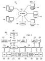
- FIG. 1 is an example block diagram of a distributed data processing system in which aspects of the illustrative embodiments may be implemented;
- FIG. 2 is an example diagram of a computing system in which aspects of the illustrative embodiments may be implemented
- FIG. 3 is a diagram illustrating a detailed framework of a phased SER prediction modeling framework in accordance with one illustrative embodiment
- FIG. 4 is a flowchart representation of the process of estimating the failure in time and rating of a chip in accordance with one illustrative embodiment
- FIG. 5 is a flowchart representation illustrating two approaches for estimating the micro-architectural workload residency of a chip in accordance with one illustrative embodiment
- FIG. 6 is a flowchart representation illustrating an in-depth micro-architectural residency gathering of a chip through a simulator in accordance with one illustrative embodiment
- FIG. 7 is a diagram illustrating a pipelined evaluation facility and the synergies thereof of applying the phased methodology to two back-to-back chip designs in accordance with one illustrative embodiment.
- chip-design begins with a consideration of system-level MTTF targets.
- the design methodology according to the illustrative embodiments is able to estimate or bound the chip-level FITs with reasonable accuracy in order to avoid in-field system quality problems.
- a balanced combination of circuit/logic-level innovations and architecture/software-level solutions are utilized to achieve the desired FIT target.
- the illustrative embodiments provide a comprehensive understanding of the vulnerabilities associated with various units on the chip with regard to workload behavior. With such information being available, appropriate approaches, such as selective duplication, SER-tolerant latch design adoption, and ECC/parity protection of SER “hotspots,” may be used for efficient reliability protection.
- An SER “hotspot” refers to a region of an IC chip that is deemed to be highly vulnerable to bit flips in an element (latch, combinational logic, or SRAM).
- the illustrative embodiments provide mechanisms and a methodology for projecting soft error vulnerability of a microprocessor design in a phased-manner across various stages of a design process.
- projections made in various phases of one system design may be proactively used to improve and shorten the projections of another system design.
- the illustrative embodiments motivated on the premise that an accurate methodology infrastructure driven by target workloads would enable cost-effective SER solutions during the design process, provides mechanisms for modeling the effects of soft errors on the micro-architectural and architectural functionality of a system.
- the framework as described hereafter in the context of illustrative embodiments, is a vehicle for developing fundamental understanding of the system-level effects of soft error rates (SER) as a microprocessor chip design evolves through the various phases of pre-concept, concept, high-level design and register transfer level (RTL) implementation.
- this next generation infrastructure toolset is used to predict device-level, e.g., chip-level, SER failure rates and study reliability-performance tradeoffs during the phased design process.
- an infrastructure framework for deriving, at one or more stages of an integrated circuit (IC) device design, SER vulnerability maps of the integrated circuit device that may be (optionally) visualized as a color-coded device floorplan that indicates the SER “hotspot” regions of the device.
- the design may be iteratively improved as the IC device design goes through the one or more stages of the design, successively enhancing the protection-level of the most vulnerable units.
- the near-optimal balance between on-device hardware recovery support and system (software) level soft error handling may be derived in order to meet system SER MTTF targets with minimal performance overhead.
- the present invention may be embodied as a system, method or computer program product. Accordingly, the present invention may take the form of an entirely hardware embodiment, an entirely software embodiment (including firmware, resident software, micro-code, etc.) or an embodiment combining software and hardware aspects that may all generally be referred to herein as a “circuit,” “module” or “system.” Furthermore, the present invention may take the form of a computer program product embodied in any tangible medium of expression having computer usable program code embodied in the medium.
- the computer-usable or computer-readable medium may be, for example but not limited to, an electronic, magnetic, optical, electromagnetic, infrared, or semiconductor system, apparatus, device, or propagation medium.
- the computer-readable medium would include the following: an electrical connection having one or more wires, a portable computer diskette, a hard disk, a random access memory (RAM), a read-only memory (ROM), an erasable programmable read-only memory (EPROM or Flash memory), an optical fiber, a portable compact disc read-only memory (CDROM), an optical storage device, a transmission media such as those supporting the Internet or an intranet, or a magnetic storage device.
- a computer-usable or computer-readable medium could even be paper or another suitable medium upon which the program is printed, as the program can be electronically captured, via, for instance, optical scanning of the paper or other medium, then compiled, interpreted, or otherwise processed in a suitable manner, if necessary, and then stored in a computer memory.
- a computer-usable or computer-readable medium may be any medium that can contain, store, communicate, propagate, or transport the program for use by or in connection with the instruction execution system, apparatus, or device.
- the computer-usable medium may include a propagated data signal with the computer-usable program code embodied therewith, either in baseband or as part of a carrier wave.
- the computer usable program code may be transmitted using any appropriate medium, including but not limited to wireless, wireline, optical fiber cable, RF, etc.
- Computer program code for carrying out operations of the present invention may be written in any combination of one or more programming languages, including an object oriented programming language such as Java, Smalltalk, C++ or the like and conventional procedural programming languages, such as the “C” programming language or similar programming languages.
- the program code may execute entirely on the user's computer, partly on the user's computer, as a stand-alone software package, partly on the user's computer and partly on a remote computer or entirely on the remote computer or server.
- the remote computer may be connected to the user's computer through any type of network, including a local area network (LAN) or a wide area network (WAN), or the connection may be made to an external computer (for example, through the Internet using an Internet Service Provider).
- LAN local area network
- WAN wide area network
- Internet Service Provider for example, AT&T, MCI, Sprint, EarthLink, MSN, GTE, etc.
- These computer program instructions may also be stored in a computer-readable medium that can direct a computer or other programmable data processing apparatus to function in a particular manner, such that the instructions stored in the computer-readable medium produce an article of manufacture including instruction means which implement the function/act specified in the flowchart and/or block diagram block or blocks.
- the computer program instructions may also be loaded onto a computer or other programmable data processing apparatus to cause a series of operational steps to be performed on the computer or other programmable apparatus to produce a computer implemented process such that the instructions which execute on the computer or other programmable apparatus provide processes for implementing the functions/acts specified in the flowchart and/or block diagram block or blocks.
- each block in the flowchart or block diagrams may represent a module, segment, or portion of code, which comprises one or more executable instructions for implementing the specified logical function(s).
- the functions noted in the block may occur out of the order noted in the figures. For example, two blocks shown in succession may, in fact, be executed substantially concurrently, or the blocks may sometimes be executed in the reverse order, depending upon the functionality involved.
- FIGS. 1 and 2 are provided hereafter as example environments in which aspects of the illustrative embodiments may be implemented. It should be appreciated that FIGS. 1-2 are only examples and are not intended to assert or imply any limitation with regard to the environments in which aspects or embodiments of the present invention may be implemented. Many modifications to the depicted environments may be made without departing from the spirit and scope of the present invention.
- FIG. 1 depicts a pictorial representation of an example distributed data processing system in which aspects of the illustrative embodiments may be implemented.
- Distributed data processing system 100 may include a network of computers in which aspects of the illustrative embodiments may be implemented.
- the distributed data processing system 100 contains at least one network 102 , which is the medium used to provide communication links between various devices and computers connected together within distributed data processing system 100 .
- the network 102 may include connections, such as wire, wireless communication links, or fiber optic cables.
- server 104 and server 106 are connected to network 102 along with storage unit 108 .
- clients 110 , 112 , and 114 are also connected to network 102 .
- These clients 110 , 112 , and 114 may be, for example, personal computers, network computers, or the like.
- server 104 provides data, such as boot files, operating system images, and applications to the clients 110 , 112 , and 114 .
- Clients 110 , 112 , and 114 are clients to server 104 in the depicted example.
- Distributed data processing system 100 may include additional servers, clients, and other devices not shown.
- distributed data processing system 100 is the Internet with network 102 representing a worldwide collection of networks and gateways that use the Transmission Control Protocol/Internet Protocol (TCP/IP) suite of protocols to communicate with one another.
- TCP/IP Transmission Control Protocol/Internet Protocol
- the distributed data processing system 100 may also be implemented to include a number of different types of networks, such as for example, an intranet, a local area network (LAN), a wide area network (WAN), or the like.
- FIG. 1 is intended as an example, not as an architectural limitation for different embodiments of the present invention, and therefore, the particular elements shown in FIG. 1 should not be considered limiting with regard to the environments in which the illustrative embodiments of the present invention may be implemented.
- Data processing system 200 is an example of a computer, such as client 110 in FIG. 1 , in which computer usable code or instructions implementing the processes for illustrative embodiments of the present invention may be located.
- data processing system 200 employs a hub architecture including north bridge and memory controller hub (NB/MCH) 202 and south bridge and input/output (I/O) controller hub (SB/ICH) 204 .
- NB/MCH north bridge and memory controller hub
- I/O input/output controller hub
- Processing unit 206 , main memory 208 , and graphics processor 210 are connected to NB/MCH 202 .
- Graphics processor 210 may be connected to NB/MCH 202 through an accelerated graphics port (AGP).
- AGP accelerated graphics port
- local area network (LAN) adapter 212 connects to SB/ICH 204 .
- Audio adapter 216 , keyboard and mouse adapter 220 , modem 222 , read only memory (ROM) 224 , hard disk drive (HDD) 226 , CD-ROM drive 230 , universal serial bus (USB) ports and other communication ports 232 , and PCI/PCIe devices 234 connect to SB/ICH 204 through bus 238 and bus 240 .
- PCI/PCIe devices may include, for example, Ethernet adapters, add-in cards, and PC cards for notebook computers. PCI uses a card bus controller, while PCIe does not.
- ROM 224 may be, for example, a flash basic input/output system (BIOS).
- HDD 226 and CD-ROM drive 230 connect to SB/ICH 204 through bus 240 .
- HDD 226 and CD-ROM drive 230 may use, for example, an integrated drive electronics (IDE) or serial advanced technology attachment (SATA) interface.
- IDE integrated drive electronics
- SATA serial advanced technology attachment
- Super I/O (SIO) device 236 may be connected to SB/ICH 204 .
- An operating system runs on processing unit 206 .
- the operating system coordinates and provides control of various components within the data processing system 200 in FIG. 2 .
- the operating system may be a commercially available operating system such as Microsoft® Windows® XP (Microsoft and Windows are trademarks of Microsoft Corporation in the United States, other countries, or both).
- An object-oriented programming system such as the JavaTM programming system, may run in conjunction with the operating system and provides calls to the operating system from JavaTM programs or applications executing on data processing system 200 (Java is a trademark of Sun Microsystems, Inc. in the United States, other countries, or both).
- data processing system 200 may be, for example, an IBM® eServerTM System P® computer system, running the Advanced Interactive Executive (AIX®) operating system or the LINUX® operating system (eServer, System p, and AIX are trademarks of International Business Machines Corporation in the United States, other countries, or both while LINUX is a trademark of Linus Torvalds in the United States, other countries, or both).
- Data processing system 200 may be a symmetric multiprocessor (SMP) system including a plurality of processors in processing unit 206 . Alternatively, a single processor system may be employed.
- SMP symmetric multiprocessor
- Instructions for the operating system, the object-oriented programming system, and applications or programs are located on storage devices, such as HDD 226 , and may be loaded into main memory 208 for execution by processing unit 206 .
- the processes for illustrative embodiments of the present invention may be performed by processing unit 206 using computer usable program code, which may be located in a memory such as, for example, main memory 208 , ROM 224 , or in one or more peripheral devices 226 and 230 , for example.
- a bus system such as bus 238 or bus 240 as shown in FIG. 2 , may be comprised of one or more buses.
- the bus system may be implemented using any type of communication fabric or architecture that provides for a transfer of data between different components or devices attached to the fabric or architecture.
- a communication unit such as modem 222 or network adapter 212 of FIG. 2 , may include one or more devices used to transmit and receive data.
- a memory may be, for example, main memory 208 , ROM 224 , or a cache such as found in NB/MCH 202 in FIG. 2 .
- FIGS. 1-2 may vary depending on the implementation.
- Other internal hardware or peripheral devices such as flash memory, equivalent non-volatile memory, or optical disk drives and the like, may be used in addition to or in place of the hardware depicted in FIGS. 1-2 .
- the processes of the illustrative embodiments may be applied to a multiprocessor data processing system, other than the SMP system mentioned previously, without departing from the spirit and scope of the present invention.
- data processing system 200 may take the form of any of a number of different data processing systems including client computing devices, server computing devices, a tablet computer, laptop computer, telephone or other communication device, a personal digital assistant (PDA), or the like.
- data processing system 200 may be a portable computing device which is configured with flash memory to provide non-volatile memory for storing operating system files and/or user-generated data, for example.
- data processing system 200 may be any known or later developed data processing system without architectural limitation.
- users of the various client computing devices 110 - 114 may collaborate on the design of an integrated circuit device using one or more tools provided by a server 104 or 106 , for example.
- the server 104 or 106 may provide a tool for modeling the system level effects of soft errors in accordance with one illustrative embodiment.
- the various tools provided by the server 104 or 106 may be provided within a stand-alone data processing system.
- the tool for modeling system level effects of soft errors integrates device-level and component-level soft error rate (SER) analysis with micro-architecture level performance analysis tools during the early phase of integrated circuit device design, e.g., the concept phase of the design.
- SER soft error rate
- the integrated circuit device being designed is an integrated circuit (IC) chip.
- IC integrated circuit
- the modeling tool framework also allows the designers to undertake “what-if” evaluations and comparisons, with a focus on adopting various latches and cells from a design library in the various units based on their respective SER vulnerability characteristics.
- the modeling tool framework further allows an architecture definition team to decide on the exact style and level of micro-architectural redundancy that may be needed to achieve per-chip SER FIT targets.
- the IC chip SER profile is refined, as more accurate information about the unit-wise latch distributions, latch types, and SER vulnerabilities of logic and latch elements become available.
- RTL register transfer level
- FIG. 3 presents a detailed overview of a framework 300 of one illustrative embodiment of the phased multi-stage prediction modeling, evaluation, and estimation framework of soft error vulnerability through the various stages of system design.
- the main methodology behind each of the phases 310 , 320 , 330 , and 340 in the framework 300 are similar with the additional impetus that as the design moves from the pre-concept phase 310 to the next higher phases 320 , 330 , and 340 , respectively, the information available and its accuracy improves, making it possible for the modeling accuracy to keep improving.
- the projections and predictions made in the previous phase can be used in a loop-back manner to improve the next phase projections and predictions, and vice versa.
- M 0 , M 1 , M 2 , and M 3 have corresponding IC chip SER workload modeling engines: Phaser/M 0 314 , Phaser/M 1 324 , Phaser/M 2 334 , and Phaser/M 3 344 , where the latch/cell types and counts, with their corresponding vulnerabilities, are combined together with the active workload residencies of the chip or component to produce respective increasingly accurate SER projections 318 , 328 , 338 , 348 , and 352 .
- a lateral iteration 316 , 326 , 336 , and 346 of improving the raw SER modeling and workload residency aids the accuracy of the SER projection at that stage.
- Workload residency is a measure of the opportune proportion of cycles during a workload execution for which bit-flip events could alter the program correctness.
- workload residency is a measure of a logic element's (average) susceptibility to soft errors; measuring the cycles during which the logic element is working on correct-path instruction execution which could affect the correctness of the workload output versus the total number of cycles of execution.
- the residency can be measured for logic elements, storage elements, etc. and may be measured at various levels of granularity from single transistors through larger accumulations (e.g. logical units, etc.).
- Residency is similar to the familiar metric of utilization, but with the additional restriction that only the utilized cycles in which the data stored or logic being computed could result in alterations of the final workload output (i.e. a soft error) are considered.
- the M 0 model 312 is an analytical performance model, e.g., a spreadsheet or the like, or a very early “cycle-approximate” simulator that is adapted from an earlier generation cycle-accurate M 1 performance model 322 .
- the architecture team arrives at a more definite view of the processor core and chip-level micro-architecture.
- the framework 300 leverages the M 1 (cycle-accurate performance) model 322 for the core to build the SER analysis tool.
- the M 1 performance model 322 is replaced by a “latch-accurate” M 2 model 332 , where the inter-unit interfaces are accurately modeled in terms of the exact latch counts.
- the intra-unit execution semantics are still written in a behavioral format, e.g., using C/C++ type languages, as in the M 1 model 322 , for example.
- the corresponding chip SER workload modeling paradigm, Phaser/M 2 334 is able to model the inter-unit error propagation effects more accurately since those interface latches and their switching activities are directly observable during the simulation of specific workloads.
- the framework SER analysis moves over to link up with the RTL (M 3 ) model 342 which contains detailed logic, latch, and timing information for the full processor.
- the framework 300 has the facility for using significantly accelerated AWAN hardware simulation 350 of the RTL model 342 , which allows for running full benchmarks if necessary, at the RTL detail level.
- AWAN hardware simulation 350 is described in Ludden et al. “Functional Verification of the POWER4 Microprocessor and POWER4 Multiprocessor Systems,” IBM Journal of Research & Development, Vol. 46, No. 1, pages 53-76, 2002, which is hereby incorporated by reference.
- the framework 300 can also leverage validation/calibration support from statistical fault injection (SFI) approaches.
- SFI statistical fault injection
- various technology elements e.g., latches, combinational logic, and memory cells
- a per-unit average architectural vulnerability factor (AVF)
- AVF architectural vulnerability factor
- the AVF is then multiplied by the unit maximum (unmasked or raw) SER to project the real, i.e. derated, SER of the unit as actually manifested in program behavior.
- unit-level error rates are added to derive the chip-level SER value, which is referred to generally as the sum of failure rates (SOFRs).
- SOFRs sum of failure rates
- a post-processing approach is used to collect all the required average residency statistics at the end of a workload run. Those statistics are then combined with the detailed information of per-unit latch distributions of specific types and protection levels, along with native technological data related to raw per-bit SER values.
- the illustrative embodiments use new data (workload residency, etc.) and metrics (raw FITS, etc.) to obtain a new measure of the IC design (i.e. susceptibility to SER) than has been previously known in post processing mechanisms.
- the AVF/SOFR approach estimates the SER of an IC chip or system in two steps. The first step, i.e.
- the AVF step estimates the SER of the individual components under the basic assumption that the probability of failure is uniform across a program execution.
- the SER of a given component in a processor chip is simply the fraction of time it holds useful work and/or data multiplied by the raw SER of the component. This fraction of time is referred to as the component value of data residency.
- the second step i.e. the SOFR step, estimates the SER of the entire IC chip or system by adding together the individual SER values of the constituent components under the general assumption that the inter-arrival time for failures is exponentially distributed.
- the methodology derives the residency factors from the corresponding simulation model, e.g., M 0 312 , M 1 322 , M 2 332 , or M 3 342 in FIG. 3 .
- the framework 300 uses a detailed method to calculate the architectural residency factors that can be implemented more practically than known methodologies while preserving accuracy. For example, a systematic method to monitor only useful register file residencies, i.e., those that contribute to actual instruction completion and modification of the architected register and memory state, is utilized.
- the term “architected” refers to the components of the machine that are accessible by software including memory, register files, special-purpose registers, and the like.
- the measured residency data is combined with the various latch, logic, and cell raw SERs of the targeted IC chip in a systematic manner to project the de-rating factors as well as the overall SER.
- FIG. 4 a flowchart representation of a process of estimating the failure in time and rating of a chip in accordance with one illustrative embodiment is depicted.
- the process outlined in FIG. 4 may be performed, for example, by the Phaser/Mi in FIG. 3 , for example.
- a quick inspection of the process 400 demonstrates that a considerable amount of data and a number of factors from various sources are factored and merged together to achieve a realistic SER and de-rating prediction model.
- the framework 300 revolves around two major approaches: (1) estimating the raw SER of the targeted IC chip or system; and (2) deriving the average residency of the typical workload executing on the same IC chip or system. These two derivations are used to accurately predict the de-rating factor and the projected SER of the IC chip or system under study.
- the raw SER of an IC chip is defined as the expected total SER assuming that the chip is busy 100% of the time and that every bit or cell upset that occurs during its operation leads to a manifested soft error.
- Accurate raw SER modeling of an IC chip or its components utilizes an in-depth knowledge of the constituent latches, array cells, and combinational logic with respect to counts and types as well as their associated vulnerabilities to soft errors. As illustrated by the process 400 in FIG.
- the framework 300 of the illustrative embodiments gathers this element and technology information 420 of the logic 421 , latch 422 , and SRAM 423 counts, as well as type data, from a design database 410 , which may be maintained, for example, in a storage device associated with the data processing system, e.g., storage 108 in FIG. 1 , hard disk 226 in FIG. 2 , or the like.
- a design database 410 which may be maintained, for example, in a storage device associated with the data processing system, e.g., storage 108 in FIG. 1 , hard disk 226 in FIG. 2 , or the like.
- information on the ratio of latches 424 and memory cells 425 protected against errors, capable of recovering from errors, as well as those that will only signal the occurrence of errors are also taken from the design database 410 . Since the framework 300 is multi-phase, it is expected that this data is updated frequently as more accurate design data becomes available with the maturity of the design.
- the Phaser/Mi component modeling computes the contribution of SER by each of the elements, e.g., logic, latches, SRAM, and the like.
- the raw SER contribution of combinational logic 430 is basically the summation of all gates multiplied by the respective gate's native raw FIT.
- the raw SER/FIT values are simple measures of the susceptibility of the basic circuit/device structures, given the technological parameters of the device (i.e. sizes of gate, oxide thickness, voltage level, doping, etc.) to be affected by various quanta of “noise” (i.e. energy that is not specifically intended data value).
- noise i.e. energy that is not specifically intended data value.
- CMOS process there is a technology team that defines a set of basic elements (the device library, which includes bit latches, basic gates, mux elements, etc.) that are used to implement the desired design.
- This design library team also runs various experiments, including electrical simulations, etc. to determine the raw susceptibility of the devices to these noise effects (of which an external strike by a galactic particle, e.g., an alpha particle, etc. is one possible source).
- Devices that are run closer to the threshold voltage, or with narrower gate channels, etc. are more susceptible, and the designers have the option to choose among a variety of different devices with different SER/FIT characteristics (among others, e.g., speed, power, etc.).
- the generation of raw SER/FIT information is a precursor to the operation of the mechanisms of the illustrative embodiments.
- This information is generally kept in the form of design database (i.e. as attributes in the design library, or externally in a database, etc.) and may or may not change occasionally as the technology becomes better characterized, or as new experiments on the basic circuit data provide better information about the raw FIT of devices.
- This data is available from each technology foundry/fabrication facility, for each design library supported.
- the illustrative embodiments take in this raw SER/FIT information and operate upon it in the manner described herein.
- the raw SER contribution of latches 440 is the summation of all latch bits multiplied by the respective latch bit's native raw FIT.
- the raw SER contribution of SRAM or storage structures 450 is the summation of all memory/storage cells multiplied by the respective cell's native raw FIT. The summation of these values 430 , 440 , and 450 give the total worst case Raw FITs 480 of the IC chip or system under study.
- de-rating refers to the portion of time an IC chip unit or structure (whether logic or storage) is not in use, or during which it is operating but in a manner that cannot affect an executing workload's correctness. Therefore, it can be said that the structure or unit is not susceptible to soft errors during that time period. This is termed de-rating because it reduces the overall opportunity for soft error vulnerability in a unit or structure from a baseline or raw SER value (derived from the underlying unit/structure hardware primitives, which does not take the specific implementation usage into account).
- a microprocessor unit with a de-rating factor of 75% over a given workload execution implies that such a unit is susceptible to errors only 25% of the total execution time of the workload run, which factor is used to reduce the baseline per-cycle susceptibility by that proportion.
- De-rating factors result from a wide set of behaviors, from low-level electrical factors (e.g., the latch duty cycle) through high-level effects (e.g., the instruction set architecture and programming conventions). Overall, de-rating refers to any of the factors that reduce the raw SER from the base value.
- the design planned protected latch ratio 424 and protected cell ratio 425 data gathered from the design database 410 , as well as information on the gate levels in the various logic chains, are used.
- the combinational logic chain SER 430 is de-rated further by knowing the actual levels and composition counts of logic gates and being able to extract the proportion of the zero to three gate type levels and counts that matter, as discussed above.
- VHDL dissecting tool e.g., a Vtiming tool 461
- RTL register transfer level
- Vtiming tool 461 An example of a Vtiming tool 461 that may be utilized with the mechanisms of the illustrative embodiments is described in Kudva et al., “Early Performance Prediction,” Proceedings of the Workshop on Complexity—Effective Design: Held in Conjunction with the 32nd International Symposium on Computer Architecture, Madison, Wis., 2005 (see www.csl.cornell.edu/albonesi/wced05/wced05.pdf), which is hereby incorporated by reference.
- the Vtiming tool 461 scans the VHDL description of the IC chip or component and gathers statistics about the number and types of logic gates within each level of a given combinational logic chain.
- the Vtiming tool 461 is able to provide an estimate of the length and number of gates in various levels of logic of a cone of logic in the early stage RTL description without the requirement of a gate level design or synthesis. Based on the number of signals that are in the input set of an output or state signal, an estimate of the number and sensitivity of combinational logic in the design can be made by the Vtiming tool 461 .
- the raw FITs contributed by the combinational logic 430 are further de-rated or masked 460 by considering only the gates in the level zero to level three of the design.
- the de-rated combinational logic raw FITs 460 are then combined with the latch and SRAM raw FITs 440 and 450 , both de-rated by the protected latch ratio 424 and protected cell ratio 450 , respectively.
- the resulting intermediate FITs 470 is considered purely micro-architecture dependent, before the effects of workload behavior are considered.
- the residency data or metrics collection process is illustrated in FIGS. 5 and 6 .
- the intermediate FITs 470 value is micro-architecturally de-rated 485 to the real (or manifested) FITs 490 .
- a comparison between the de-rated (real) FITs 490 and the total worst case Raw FITs 480 generates the net de-rating factor estimate 492 . It should be noted that the methodology as described has been with a focus on silent data corruption (SDC)-related SER manifested at the program output.
- SDC silent data corruption
- FIG. 5 a flowchart representation illustrating two approaches for estimating the micro-architectural workload residency of a chip in accordance with one illustrative embodiment is depicted.
- Structures in a microprocessor IC chip can be broadly classified into two major groups: logic and storage.
- Logic structures can be defined to be the various data and control processing units on the IC chip that are made up of combinational logic gates and latches.
- Typical examples of on-chip logic structures then include the fixed-point unit (FXU) pipelined logic datapath (with its associated control logic) and the instruction decode unit (IDU) logic.
- Storage is defined to be the various structures that hold data values, such as the queues, register files, and other SRAM macros, for example.
- latches may also serve as staging and data-hold resources, especially during stalls in a pipeline flow.
- latch banks may also be categorized within the storage class.
- the residency modeling for such pipeline latches is simpler than register files and arrays and is better treated under the logic category.
- Workload residency modeling 500 attempts to measure the opportune proportion of cycles during a workload execution for which bit-flip events could alter program correctness.
- the focus includes only the true path of program execution. For example, dataflow-centric soft errors on a wrongly speculated path during program execution cannot alter program output. Similarly, rejected or flushed executions, dead instructions, NOPs (no operations), and performance-enhancing instructions (e.g., those related to data pre-fetch) do not contribute to SER-induced data corruption.
- the question that is asked is, during what fraction of the cycles is there an operation that uses a particular logic structure in such a manner as to lead to actual completed instructions?
- the question is, during what fraction of cycles is the storage resource holding a value that will subsequently be used in the true execution path?
- microarchitecture utilization When it comes to SER modeling, there are often attempts to use microarchitecture utilization as a proxy for actual residency. However, a close examination of utilization and residency in a complex microprocessor pipeline shows a potentially significant difference between the two.
- corrective factors e.g., use of average stall event or dead instruction statistics
- the effective correction factors to the computed utilization data in proxy for residency may be awkward and error-prone to derive individually via average statistical behavior alone.
- the micro-architecture simulator is accurately instrumented for gathering actual residency data as shown in FIG. 5 .
- a scroll pipe output is a representation of the timing state of instructions or internal operations moving through the microprocessor pipeline.
- FIG. 6 a flowchart representation illustrating an in-depth micro-architectural residency gathering of an IC chip through a simulator in accordance with one illustrative embodiment is depicted.
- the operation outlined in FIG. 6 may be an in-depth illustration of the operations performed as part of elements 520 or 545 in FIG. 5 , which again may be performed by the Mi models.
- the process 600 in FIG. 6 illustrates an example of the detailed residency gathering operations within a performance simulator or a scroll pipe analyzer. Basically, each instruction records significant event times during simulated execution, and these per-instruction metrics are gathered when an instruction completes.
- the analysis tool starts at the first pipeline stage 615 and considers each pipeline stage in turn 655 .
- a determination is made as to whether an instruction is first entering that pipeline stage 620 . If there is an instruction entering that stage, the time of the instruction's entry into the stage (i.e., the current cycle of simulation) is recorded in the instruction's internal data structure (e.g., a lop data structure) 625 .
- a determination is then made as to whether an instruction is leaving the pipeline stage 630 . If so, then the time of the instruction's exit from the stage (i.e., the current cycle of simulation) is recorded in the instruction's internal data structure (e.g., a lop data structure) 635 .
- illustrative embodiments present a phased methodology framework that allows progressive refinement of soft-error related de-rating and failure in time analysis as the design progresses from (pre)concept phase to high-level design phase and the RTL implementation phase.
- the methodology renders itself to a pipelined evaluative framework that allows quicker start of SER analysis for a next generation microprocessor IC chip design starting off from the present phase of a current design, enabling higher design/evaluation throughput in a multi-chip design process.
- the illustrative embodiments provide a quicker start of SER analysis because a higher-level analysis on an earlier-availability model is performed.
- SER analysis have historically been done using VHDL and/or RTL models which are often only available very late in the design process or cycle, or perhaps even only after initial fabrication of actual IC hardware.
- approach of the illustrative embodiments enables SER modeling using the early design models, and even the earliest design-space exploration models, which are available very early in the design process.
- the illustrative embodiments enable the capability to consider SER effects from the very earliest stages of the design of a new microprocessor core or system.
- the results of this analysis may be used in many different ways.
- the results of the SER analysis may be used to determine more robust system options (i.e. affecting the actual design selected, by providing a way to compare SER vulnerability across designs) through identification of high-vulnerability structures.
- the results of the SER analysis may be used to perform trade-off analysis in the addition of SER vulnerability mitigation mechanisms.
- the results of the SER analysis may indicate the need to use of parity bit and error correcting code (ECC) checkers as well as the use of radiation-hardened latches in various parts of the IC chip.
- ECC error correcting code
- two IC chip design projects 710 and 720 may be run in-step in a pipelined fashion where chip A 710 is always a phase ahead of chip B 720 .
- the SER analysis for chip A 710 at the pre-concept phase starts off with the necessary application and technology parameters 711 .
- chip A exits the pre-concept phase its pre-concept phase analysis output 732 and its scaled application and technology parameter data 711 are combined with chip B's tentative application and technology parameter data 721 to start off chip B's pre-concept phase SER analysis.
- the information from chip A 710 can help in making the analysis for chip B 720 both more accurate and quicker.
- Chip A's concept phase output 732 is combined with chip B's pre-concept phase analysis output in feeding chip B's concept phase analysis.
- the same process continues in feeding chip A's next two phases outputs 733 and 734 with chip B's previous outputs in effecting chip B's next phases' SER analysis outputs. The process continues this way until chip A's final SER analysis output 715 is derived and then a phase later, chip B's final SER analysis output 725 is derived.
- the illustrative embodiments may take the form of an entirely hardware embodiment, an entirely software embodiment or an embodiment containing both hardware and software elements.
- the mechanisms of the illustrative embodiments are implemented in software or program code, which includes but is not limited to firmware, resident software, microcode, etc.
- a data processing system suitable for storing and/or executing program code will include at least one processor coupled directly or indirectly to memory elements through a system bus.
- the memory elements can include local memory employed during actual execution of the program code, bulk storage, and cache memories which provide temporary storage of at least some program code in order to reduce the number of times code must be retrieved from bulk storage during execution.
- I/O devices can be coupled to the system either directly or through intervening I/O controllers.
- Network adapters may also be coupled to the system to enable the data processing system to become coupled to other data processing systems or remote printers or storage devices through intervening private or public networks. Modems, cable modems and Ethernet cards are just a few of the currently available types of network adapters.
Landscapes
- Engineering & Computer Science (AREA)
- Computer Hardware Design (AREA)
- Physics & Mathematics (AREA)
- Theoretical Computer Science (AREA)
- Microelectronics & Electronic Packaging (AREA)
- Evolutionary Computation (AREA)
- Geometry (AREA)
- General Engineering & Computer Science (AREA)
- General Physics & Mathematics (AREA)
- Design And Manufacture Of Integrated Circuits (AREA)
Abstract
Description
Claims (20)
Priority Applications (1)
| Application Number | Priority Date | Filing Date | Title |
|---|---|---|---|
| US12/243,427 US8091050B2 (en) | 2008-10-01 | 2008-10-01 | Modeling system-level effects of soft errors |
Applications Claiming Priority (1)
| Application Number | Priority Date | Filing Date | Title |
|---|---|---|---|
| US12/243,427 US8091050B2 (en) | 2008-10-01 | 2008-10-01 | Modeling system-level effects of soft errors |
Publications (2)
| Publication Number | Publication Date |
|---|---|
| US20100083203A1 US20100083203A1 (en) | 2010-04-01 |
| US8091050B2 true US8091050B2 (en) | 2012-01-03 |
Family
ID=42059049
Family Applications (1)
| Application Number | Title | Priority Date | Filing Date |
|---|---|---|---|
| US12/243,427 Expired - Fee Related US8091050B2 (en) | 2008-10-01 | 2008-10-01 | Modeling system-level effects of soft errors |
Country Status (1)
| Country | Link |
|---|---|
| US (1) | US8091050B2 (en) |
Cited By (4)
| Publication number | Priority date | Publication date | Assignee | Title |
|---|---|---|---|---|
| US8745567B1 (en) * | 2013-03-14 | 2014-06-03 | Atrenta, Inc. | Efficient apparatus and method for analysis of RTL structures that cause physical congestion |
| US10318406B2 (en) * | 2017-02-23 | 2019-06-11 | International Business Machines Corporation | Determine soft error resilience while verifying architectural compliance |
| US20220114075A1 (en) * | 2017-08-30 | 2022-04-14 | Nvidia Corporation | Liveness as a factor to evaluate memory vulnerability to soft errors |
| US20240402246A1 (en) * | 2023-05-31 | 2024-12-05 | International Business Machines Corporation | Error protection analysis of an integrated circuit |
Families Citing this family (15)
| Publication number | Priority date | Publication date | Assignee | Title |
|---|---|---|---|---|
| US8555234B2 (en) * | 2009-09-03 | 2013-10-08 | International Business Machines Corporation | Verification of soft error resilience |
| JP5585221B2 (en) * | 2010-06-08 | 2014-09-10 | 株式会社日立製作所 | Simulation apparatus and method |
| US8645796B2 (en) * | 2010-06-24 | 2014-02-04 | International Business Machines Corporation | Dynamic pipeline cache error correction |
| FR2978575B1 (en) * | 2011-07-27 | 2016-11-25 | European Aeronautic Defence & Space Co Eads France | METHOD FOR CHARACTERIZING THE SENSITIVITY OF AN ELECTRONIC COMPONENT FOR A METHOD FOR DESIGNING ELECTRONIC EQUIPMENT |
| US8949101B2 (en) * | 2011-10-12 | 2015-02-03 | International Business Machines Corporation | Hardware execution driven application level derating calculation for soft error rate analysis |
| US9384117B2 (en) * | 2013-03-01 | 2016-07-05 | Infineon Technologies Ag | Machine and methods for evaluating failing software programs |
| US9075904B2 (en) | 2013-03-13 | 2015-07-07 | Intel Corporation | Vulnerability estimation for cache memory |
| US8943458B1 (en) * | 2013-09-16 | 2015-01-27 | International Business Machines Corporation | Determining chip burn-in workload using emulated application condition |
| US20160171140A1 (en) * | 2014-12-11 | 2016-06-16 | Freescale Semiconductor, Inc. | Method and system for determining minimum operational voltage for transistor memory-based devices |
| US9652350B2 (en) * | 2015-01-22 | 2017-05-16 | International Business Machines Corporation | Evaluation of complex SAN environments |
| EP3136268B1 (en) * | 2015-08-31 | 2019-06-19 | Siemens Aktiengesellschaft | Method for analyzing the security of a logic circuit |
| JP6675359B2 (en) * | 2017-09-04 | 2020-04-01 | 富士フイルム株式会社 | Recording control device, recording control method, and recording tape cartridge |
| CN111274058B (en) * | 2020-01-20 | 2024-04-02 | 东南大学 | Lightweight redundant assertion screening method |
| US11416166B2 (en) * | 2020-06-26 | 2022-08-16 | Western Digital Technologies, Inc. | Distributed function processing with estimate-based scheduler |
| CN117993337B (en) * | 2024-03-12 | 2024-12-27 | 沐曦科技(成都)有限公司 | RTL static verification system |
Citations (8)
| Publication number | Priority date | Publication date | Assignee | Title |
|---|---|---|---|---|
| US20010039642A1 (en) * | 2000-04-28 | 2001-11-08 | Nec Corporation | Design system for flip chip semiconductor device |
| US6986078B2 (en) | 2002-08-07 | 2006-01-10 | International Business Machines Corporation | Optimization of storage and power consumption with soft error predictor-corrector |
| US7203881B1 (en) | 2004-06-29 | 2007-04-10 | Sun Microsystems, Inc. | System and method for simulating system operation |
| US20080016477A1 (en) * | 2006-07-13 | 2008-01-17 | Kleinosowski Aj | Method for Soft Error Modeling with Double Current Pulse |
| US7328376B2 (en) | 2003-10-31 | 2008-02-05 | Sun Microsystems, Inc. | Error reporting to diagnostic engines based on their diagnostic capabilities |
| US20080191769A1 (en) * | 2005-09-22 | 2008-08-14 | Fujitsu Limited | Signal transmission circuit, semiconductor device that includes the signal transmission circuit, method for designing the semiconductor circuit device, and cad device |
| US7472051B2 (en) * | 2003-07-11 | 2008-12-30 | Yogitech Spa | Dependable microcontroller, method for designing a dependable microcontroller and computer program product therefor |
| US20090249301A1 (en) | 2008-03-31 | 2009-10-01 | International Business Machines Corporation | Method and Apparatus for Testing Soft Error Rate of an Application Program |
Family Cites Families (1)
| Publication number | Priority date | Publication date | Assignee | Title |
|---|---|---|---|---|
| EP1353333A1 (en) * | 2002-04-12 | 2003-10-15 | STMicroelectronics S.r.l. | Shaped spectral coding and recording systems therefor |
-
2008
- 2008-10-01 US US12/243,427 patent/US8091050B2/en not_active Expired - Fee Related
Patent Citations (8)
| Publication number | Priority date | Publication date | Assignee | Title |
|---|---|---|---|---|
| US20010039642A1 (en) * | 2000-04-28 | 2001-11-08 | Nec Corporation | Design system for flip chip semiconductor device |
| US6986078B2 (en) | 2002-08-07 | 2006-01-10 | International Business Machines Corporation | Optimization of storage and power consumption with soft error predictor-corrector |
| US7472051B2 (en) * | 2003-07-11 | 2008-12-30 | Yogitech Spa | Dependable microcontroller, method for designing a dependable microcontroller and computer program product therefor |
| US7328376B2 (en) | 2003-10-31 | 2008-02-05 | Sun Microsystems, Inc. | Error reporting to diagnostic engines based on their diagnostic capabilities |
| US7203881B1 (en) | 2004-06-29 | 2007-04-10 | Sun Microsystems, Inc. | System and method for simulating system operation |
| US20080191769A1 (en) * | 2005-09-22 | 2008-08-14 | Fujitsu Limited | Signal transmission circuit, semiconductor device that includes the signal transmission circuit, method for designing the semiconductor circuit device, and cad device |
| US20080016477A1 (en) * | 2006-07-13 | 2008-01-17 | Kleinosowski Aj | Method for Soft Error Modeling with Double Current Pulse |
| US20090249301A1 (en) | 2008-03-31 | 2009-10-01 | International Business Machines Corporation | Method and Apparatus for Testing Soft Error Rate of an Application Program |
Non-Patent Citations (13)
| Title |
|---|
| Bender, C. et al., "Soft-error resilience of the IBM POWERS processor input/output subsystem", IBM J. Res. & Dev., vol. 52, No. 3, May 2008, pp. 285-292. |
| Kanawati, Nasser A. et al., "Dependability Evaluation using Hybrid Fault/Error lnjection", lEEE, 1995, pp. 224-233. |
| Kellington, Jeffrey W. et al., "IBM POWERS Processor Soft Error Tolerance Analysis Using Proton Irradiation", domino.research/ibm.com/comm/research, IBM Sys & Techgy GP, Austin, TX, 2007, 6 pages. |
| Kudva et al., "Early Performance Prediction", Proceedings of the Workshop on Complexity-Effective Design: Held in Conjunction with the 32nd International Symposium on Computer Architecture, 2005, www.csl.cornell.edu/albonesi/wced05/wced05.pdf, pp. 1-18. |
| Kudva, P. et al., "Fault Injection Verification of IBM POWERS Soft Error Resilience", citeseerx.ist.psu.edu/viewdoc/download, 2006, 4 pages. |
| Li et al., "Architecture-Level Soft Error Analysis: Examining the Limits of Common Assumptions", Proceedings of the 37th Annual IEEE/IFIP International Conference on Dependable Systems and Networks (DSN'07), Jun. 2007, pp. 266-275. |
| Li, Xiaodong et al., "Scaling of Architecture Level Soft Error Rate for Superscalar Processors", rsim.cs.illinois,edu/pubs/05selse.pdf, 2005, pp. 1-7. |
| Li, Xiaodong et al., "SoftArch: An Architecture-Level Tool for Modeling and Analyzing Soft Errors", IEEE, DSN'05 Proceedings of 2005 Intern't Conf On Dependable Sys & Networks, 2005, 10 pages. |
| Ludden et al., "Functional verification of the POWER4 microprocessor and POWER4 multiprocessor systems", IBM Corporation, IBM J. Res. & Dev., vol. 46, No. 1, Jan. 2002, pp. 53-76. |
| Ma, Zhe et al., "System-level analysis of soft error rate and mitigation trade-off explorations", Reliability Physics Symposium (IRPS), 2010 IEEE Interna'l, Jun. 17, 2010, pp. 1-5. |
| Mukherjee et al., "A Systematic Methodology to Compute the Architectural Vulnerability Factors for a High-Performance Microprocessor", Proceedings of the 36th Annual IEEE/ACM International Symposium on Microarchitecture (MICRO), Dec. 2003, pp. 29-40. |
| Ramachandran, Pradeep et al., "Statistical Fault Injection", In Proc. Int'l Conf. on Dependable Systems mand Networks (DSN), Jun. 2008, 6 pages. |
| USPTO U.S. Appl. No. 13/271,827, Image File Wrapper printed Nov. 11, 2011, 1 page. |
Cited By (7)
| Publication number | Priority date | Publication date | Assignee | Title |
|---|---|---|---|---|
| US8745567B1 (en) * | 2013-03-14 | 2014-06-03 | Atrenta, Inc. | Efficient apparatus and method for analysis of RTL structures that cause physical congestion |
| US10318406B2 (en) * | 2017-02-23 | 2019-06-11 | International Business Machines Corporation | Determine soft error resilience while verifying architectural compliance |
| US10896118B2 (en) | 2017-02-23 | 2021-01-19 | International Business Machines Corporation | Determine soft error resilience while verifying architectural compliance |
| US20220114075A1 (en) * | 2017-08-30 | 2022-04-14 | Nvidia Corporation | Liveness as a factor to evaluate memory vulnerability to soft errors |
| US11720472B2 (en) * | 2017-08-30 | 2023-08-08 | Nvidia Corporation | Liveness as a factor to evaluate memory vulnerability to soft errors |
| US20240402246A1 (en) * | 2023-05-31 | 2024-12-05 | International Business Machines Corporation | Error protection analysis of an integrated circuit |
| US12188979B2 (en) * | 2023-05-31 | 2025-01-07 | International Business Machines Corporation | Error protection analysis of an integrated circuit |
Also Published As
| Publication number | Publication date |
|---|---|
| US20100083203A1 (en) | 2010-04-01 |
Similar Documents
| Publication | Publication Date | Title |
|---|---|---|
| US8091050B2 (en) | Modeling system-level effects of soft errors | |
| US8949101B2 (en) | Hardware execution driven application level derating calculation for soft error rate analysis | |
| Zhang et al. | FASER: Fast analysis of soft error susceptibility for cell-based designs | |
| Chatzidimitriou et al. | Multi-bit upsets vulnerability analysis of modern microprocessors | |
| Kaliorakis et al. | Merlin: Exploiting dynamic instruction behavior for fast and accurate microarchitecture level reliability assessment | |
| Holcomb et al. | Design as you see FIT: System-level soft error analysis of sequential circuits | |
| Vallero et al. | Cross-layer system reliability assessment framework for hardware faults | |
| Ottavi et al. | Dependable multicore architectures at nanoscale: The view from europe | |
| Tanikella et al. | gemV: A validated toolset for the early exploration of system reliability | |
| Sari et al. | A fault injection platform for the analysis of soft error effects in FPGA soft processors | |
| Saggese et al. | Microprocessor sensitivity to failures: control vs. execution and combinational vs. sequential logic | |
| Deutsch et al. | Delayavf: Calculating architectural vulnerability factors for delay faults | |
| Wali et al. | A low-cost reliability vs. cost trade-off methodology to selectively harden logic circuits | |
| Ma et al. | Proactive Runtime Detection of Aging-Related Silent Data Corruptions: A Bottom-Up Approach | |
| Chandra | Monitoring reliability in embedded processors-a multi-layer view | |
| Jenihhin et al. | Towards multidimensional verification: Where functional meets non-functional | |
| Wang et al. | Fast reliability exploration for embedded processors via high-level fault injection | |
| Herkersdorf et al. | Cross-layer dependability modeling and abstraction in system on chip | |
| Portolan et al. | Alternatives to fault injections for early safety/security evaluations | |
| Shojaei et al. | Trace signal selection to enhance timing and logic visibility in post-silicon validation | |
| Choudhury et al. | Masking timing errors on speed-paths in logic circuits | |
| Rivers et al. | Phaser: Phased methodology for modeling the system-level effects of soft errors | |
| Taatizadeh et al. | Emulation infrastructure for the evaluation of hardware assertions for post-silicon validation | |
| Azarpeyvand et al. | Fast and accurate architectural vulnerability analysis for embedded processors using instruction vulnerability factor | |
| Zandian et al. | Wearmon: Reliability monitoring using adaptive critical path testing |
Legal Events
| Date | Code | Title | Description |
|---|---|---|---|
| AS | Assignment |
Owner name: INTERNATIONAL BUSINESS MACHINES CORPORATION,NEW YO Free format text: ASSIGNMENT OF ASSIGNORS INTEREST;ASSIGNORS:BOSE, PRADIP;KUDVA, PRABHAKAR N.;RIVERS, JUDE A.;AND OTHERS;SIGNING DATES FROM 20080902 TO 20080905;REEL/FRAME:021621/0001 Owner name: INTERNATIONAL BUSINESS MACHINES CORPORATION, NEW Y Free format text: ASSIGNMENT OF ASSIGNORS INTEREST;ASSIGNORS:BOSE, PRADIP;KUDVA, PRABHAKAR N.;RIVERS, JUDE A.;AND OTHERS;SIGNING DATES FROM 20080902 TO 20080905;REEL/FRAME:021621/0001 |
|
| STCF | Information on status: patent grant |
Free format text: PATENTED CASE |
|
| FPAY | Fee payment |
Year of fee payment: 4 |
|
| SULP | Surcharge for late payment | ||
| AS | Assignment |
Owner name: GLOBALFOUNDRIES U.S. 2 LLC, NEW YORK Free format text: ASSIGNMENT OF ASSIGNORS INTEREST;ASSIGNOR:INTERNATIONAL BUSINESS MACHINES CORPORATION;REEL/FRAME:036550/0001 Effective date: 20150629 |
|
| AS | Assignment |
Owner name: GLOBALFOUNDRIES INC., CAYMAN ISLANDS Free format text: ASSIGNMENT OF ASSIGNORS INTEREST;ASSIGNORS:GLOBALFOUNDRIES U.S. 2 LLC;GLOBALFOUNDRIES U.S. INC.;REEL/FRAME:036779/0001 Effective date: 20150910 |
|
| AS | Assignment |
Owner name: WILMINGTON TRUST, NATIONAL ASSOCIATION, DELAWARE Free format text: SECURITY AGREEMENT;ASSIGNOR:GLOBALFOUNDRIES INC.;REEL/FRAME:049490/0001 Effective date: 20181127 |
|
| FEPP | Fee payment procedure |
Free format text: MAINTENANCE FEE REMINDER MAILED (ORIGINAL EVENT CODE: REM.); ENTITY STATUS OF PATENT OWNER: LARGE ENTITY |
|
| LAPS | Lapse for failure to pay maintenance fees |
Free format text: PATENT EXPIRED FOR FAILURE TO PAY MAINTENANCE FEES (ORIGINAL EVENT CODE: EXP.); ENTITY STATUS OF PATENT OWNER: LARGE ENTITY |
|
| STCH | Information on status: patent discontinuation |
Free format text: PATENT EXPIRED DUE TO NONPAYMENT OF MAINTENANCE FEES UNDER 37 CFR 1.362 |
|
| FP | Lapsed due to failure to pay maintenance fee |
Effective date: 20200103 |
|
| AS | Assignment |
Owner name: GLOBALFOUNDRIES INC., CAYMAN ISLANDS Free format text: RELEASE BY SECURED PARTY;ASSIGNOR:WILMINGTON TRUST, NATIONAL ASSOCIATION;REEL/FRAME:054636/0001 Effective date: 20201117 |
|
| AS | Assignment |
Owner name: GLOBALFOUNDRIES U.S. INC., NEW YORK Free format text: RELEASE BY SECURED PARTY;ASSIGNOR:WILMINGTON TRUST, NATIONAL ASSOCIATION;REEL/FRAME:056987/0001 Effective date: 20201117 Owner name: GLOBALFOUNDRIES U.S. INC., NEW YORK Free format text: RELEASE OF SECURITY INTEREST;ASSIGNOR:WILMINGTON TRUST, NATIONAL ASSOCIATION;REEL/FRAME:056987/0001 Effective date: 20201117 |