EP3135676A1 - Electroluminescent organic compounds for organic electric elements and electronic devices - Google Patents
Electroluminescent organic compounds for organic electric elements and electronic devices Download PDFInfo
- Publication number
- EP3135676A1 EP3135676A1 EP16153411.0A EP16153411A EP3135676A1 EP 3135676 A1 EP3135676 A1 EP 3135676A1 EP 16153411 A EP16153411 A EP 16153411A EP 3135676 A1 EP3135676 A1 EP 3135676A1
- Authority
- EP
- European Patent Office
- Prior art keywords
- group
- organic
- ring
- formula
- substituted
- Prior art date
- Legal status (The legal status is an assumption and is not a legal conclusion. Google has not performed a legal analysis and makes no representation as to the accuracy of the status listed.)
- Granted
Links
- 0 *C1(*)c(cccc2)c2-c2ccccc12 Chemical compound *C1(*)c(cccc2)c2-c2ccccc12 0.000 description 8
- RSQSESGFUZXJNM-UHFFFAOYSA-N c(cc12)ccc1[nH]c1c2c(cccc2)c2c2c1[s]c1ccccc21 Chemical compound c(cc12)ccc1[nH]c1c2c(cccc2)c2c2c1[s]c1ccccc21 RSQSESGFUZXJNM-UHFFFAOYSA-N 0.000 description 3
- DQKKEYGSOIIAAD-UHFFFAOYSA-N Clc1nc(-c(cc2)ccc2-c2ccccc2)c(c(cccc2)c2cc2)c2n1 Chemical compound Clc1nc(-c(cc2)ccc2-c2ccccc2)c(c(cccc2)c2cc2)c2n1 DQKKEYGSOIIAAD-UHFFFAOYSA-N 0.000 description 2
- WJVSUNDYOGLZMI-UHFFFAOYSA-N Clc1nc(-c2ccccc2)c(c(cccc2)c2cc2)c2n1 Chemical compound Clc1nc(-c2ccccc2)c(c(cccc2)c2cc2)c2n1 WJVSUNDYOGLZMI-UHFFFAOYSA-N 0.000 description 2
- QVRGGAUEEZOTCD-UHFFFAOYSA-N Brc1cc([s]c2ccccc22)c2c2c1cccc2 Chemical compound Brc1cc([s]c2ccccc22)c2c2c1cccc2 QVRGGAUEEZOTCD-UHFFFAOYSA-N 0.000 description 1
- YGBRCIZACIFRGO-HKBQPEDESA-N C([C@H]1c2ccccc22)C(c(cc34)ccc3[nH]c3c4c(cccc4)c4c4c3[o]c3c4cccc3)=CC=C1N2c1ccccc1 Chemical compound C([C@H]1c2ccccc22)C(c(cc34)ccc3[nH]c3c4c(cccc4)c4c4c3[o]c3c4cccc3)=CC=C1N2c1ccccc1 YGBRCIZACIFRGO-HKBQPEDESA-N 0.000 description 1
- BAHBAHDIHBYTRS-UHFFFAOYSA-N CC(C1)C=Cc2c1c(-c1ccccc1[N+]([O-])=O)cc1c2c(cccc2)c2[s]1 Chemical compound CC(C1)C=Cc2c1c(-c1ccccc1[N+]([O-])=O)cc1c2c(cccc2)c2[s]1 BAHBAHDIHBYTRS-UHFFFAOYSA-N 0.000 description 1
- TWDJNZHXQFVHBF-UHFFFAOYSA-N CC(C1)C=Cc2c1c(c(cccc1)c1c(c1cc(-c3ccccc3)ccc11)c3[n]1-c1nc(-c(cc4c5c6cccc5)ccc4[n]6-c4ccccc4)c(c(cccc4)c4c4c5cccc4)c5n1)c3[o]2 Chemical compound CC(C1)C=Cc2c1c(c(cccc1)c1c(c1cc(-c3ccccc3)ccc11)c3[n]1-c1nc(-c(cc4c5c6cccc5)ccc4[n]6-c4ccccc4)c(c(cccc4)c4c4c5cccc4)c5n1)c3[o]2 TWDJNZHXQFVHBF-UHFFFAOYSA-N 0.000 description 1
- SPRSGWZEQYDIBF-UHFFFAOYSA-N CC(C12)C(c(cc3)cc(c4ccccc44)c3[n]4-c3ccccc3)=CC=C1Nc1c2c(cccc2)c2c2c1[s]c1ccccc21 Chemical compound CC(C12)C(c(cc3)cc(c4ccccc44)c3[n]4-c3ccccc3)=CC=C1Nc1c2c(cccc2)c2c2c1[s]c1ccccc21 SPRSGWZEQYDIBF-UHFFFAOYSA-N 0.000 description 1
- VSCPYNBEZQFZLO-WAMHVZOESA-N CC(CC(C)=[O]1)O/C1=C(/C1C2=C3CCC=C2)\C1(C1)N=C3C(C)=Cc2c1cccc2 Chemical compound CC(CC(C)=[O]1)O/C1=C(/C1C2=C3CCC=C2)\C1(C1)N=C3C(C)=Cc2c1cccc2 VSCPYNBEZQFZLO-WAMHVZOESA-N 0.000 description 1
- TUTFDACLAAOZER-UHFFFAOYSA-N CC(Cc1c2c3c4)C=Cc1c(c(cccc1)c1[s]1)c1c2[nH]c3ccc4-c1ccccc1 Chemical compound CC(Cc1c2c3c4)C=Cc1c(c(cccc1)c1[s]1)c1c2[nH]c3ccc4-c1ccccc1 TUTFDACLAAOZER-UHFFFAOYSA-N 0.000 description 1
- CUKRYHZYNJITEX-UHFFFAOYSA-N CC1(C)c(cc(cc2)-c3c(ccc4c5cccc4)c5nc(-c(cc4C(C)(C)c5c6)ccc4-c5ccc6-[n](c4ccccc44)c5c4c4ccccc4c4c5[s]c5c4cccc5)n3)c2-c2ccccc12 Chemical compound CC1(C)c(cc(cc2)-c3c(ccc4c5cccc4)c5nc(-c(cc4C(C)(C)c5c6)ccc4-c5ccc6-[n](c4ccccc44)c5c4c4ccccc4c4c5[s]c5c4cccc5)n3)c2-c2ccccc12 CUKRYHZYNJITEX-UHFFFAOYSA-N 0.000 description 1
- UXZONRVAOXQSNS-UHFFFAOYSA-N CC1(C)c2cc(-c3nc(-[n](c(c4c5)ccc5C(CC5(C)c6ccccc66)=CC=C5N6C5=CC=CCC5)c5c4c(cccc4)c4c4c5[o]c5ccccc45)nc4c(cccc5)c5c(cccc5)c5c34)ccc2-c2c1cccc2 Chemical compound CC1(C)c2cc(-c3nc(-[n](c(c4c5)ccc5C(CC5(C)c6ccccc66)=CC=C5N6C5=CC=CCC5)c5c4c(cccc4)c4c4c5[o]c5ccccc45)nc4c(cccc5)c5c(cccc5)c5c34)ccc2-c2c1cccc2 UXZONRVAOXQSNS-UHFFFAOYSA-N 0.000 description 1
- BPOYEYHTNGZKOO-UHFFFAOYSA-N CC12c(c(cccc3)c3c3c4[s]c5c3cccc5)c4NC1=CC=CC2 Chemical compound CC12c(c(cccc3)c3c3c4[s]c5c3cccc5)c4NC1=CC=CC2 BPOYEYHTNGZKOO-UHFFFAOYSA-N 0.000 description 1
- OLIABZYLSHSPLQ-UHFFFAOYSA-N CC1c(cccc2)c2C(c2c(c(cccc3)c3cc3)c3nc(Cl)n2)=CC1 Chemical compound CC1c(cccc2)c2C(c2c(c(cccc3)c3cc3)c3nc(Cl)n2)=CC1 OLIABZYLSHSPLQ-UHFFFAOYSA-N 0.000 description 1
- NPUBDPDASOEIOA-UHFFFAOYSA-N CCB1OC(C)(C)C(C)(C)O1 Chemical compound CCB1OC(C)(C)C(C)(C)O1 NPUBDPDASOEIOA-UHFFFAOYSA-N 0.000 description 1
- WSPVKOWKZOGPIX-UHFFFAOYSA-N Clc1nc(-c2cc3ccccc3cc2)c(c(cccc2)c2cc2)c2n1 Chemical compound Clc1nc(-c2cc3ccccc3cc2)c(c(cccc2)c2cc2)c2n1 WSPVKOWKZOGPIX-UHFFFAOYSA-N 0.000 description 1
- BTYPPKDZHXQEEV-UHFFFAOYSA-N O=CS1c2ccccc2C2=C1CC=C=C2 Chemical compound O=CS1c2ccccc2C2=C1CC=C=C2 BTYPPKDZHXQEEV-UHFFFAOYSA-N 0.000 description 1
- AIIFTKAURXNERI-UHFFFAOYSA-N c(cc1)cc2c1[nH]c1c2c(cccc2)c2c2c1[o]c1c2cccc1 Chemical compound c(cc1)cc2c1[nH]c1c2c(cccc2)c2c2c1[o]c1c2cccc1 AIIFTKAURXNERI-UHFFFAOYSA-N 0.000 description 1
- PLTSFEJOUKBUNH-UHFFFAOYSA-N c(cc1)cc2c1[o]c1c2c2ccccc2c(c(c2c3)ccc3-c3ccccn3)c1[n]2-c1nc2c(cccc3)c3c(cccc3)c3c2c(-c2ncccc2)n1 Chemical compound c(cc1)cc2c1[o]c1c2c2ccccc2c(c(c2c3)ccc3-c3ccccn3)c1[n]2-c1nc2c(cccc3)c3c(cccc3)c3c2c(-c2ncccc2)n1 PLTSFEJOUKBUNH-UHFFFAOYSA-N 0.000 description 1
- BGFYZJJOLRWLPE-UHFFFAOYSA-N c(cc1)ccc1-c(cc1)ccc1-c1nc(-[n]2c3c4[s]c(cccc5)c5c4c(cccc4)c4c3c3c2cccc3)nc2ccc(cccc3)c3c12 Chemical compound c(cc1)ccc1-c(cc1)ccc1-c1nc(-[n]2c3c4[s]c(cccc5)c5c4c(cccc4)c4c3c3c2cccc3)nc2ccc(cccc3)c3c12 BGFYZJJOLRWLPE-UHFFFAOYSA-N 0.000 description 1
- RXXADLGQLSGNTB-UHFFFAOYSA-N c(cc1)ccc1-c1c(c(cccc2)c2cc2)c2nc(-[n](c2ccccc22)c3c2c(cccc2)c2c2c3[s]c3ccccc23)n1 Chemical compound c(cc1)ccc1-c1c(c(cccc2)c2cc2)c2nc(-[n](c2ccccc22)c3c2c(cccc2)c2c2c3[s]c3ccccc23)n1 RXXADLGQLSGNTB-UHFFFAOYSA-N 0.000 description 1
- FEIYKHKSAUVHAK-UHFFFAOYSA-N c(cc1)ccc1-c1c(ccc2c3cccc2)c3nc(-c(cc2)ccc2-[n](c2ccccc22)c3c2c2ccccc2c2c3[s]c3c2cccc3)n1 Chemical compound c(cc1)ccc1-c1c(ccc2c3cccc2)c3nc(-c(cc2)ccc2-[n](c2ccccc22)c3c2c2ccccc2c2c3[s]c3c2cccc3)n1 FEIYKHKSAUVHAK-UHFFFAOYSA-N 0.000 description 1
- BFHFMJZRKJQEBS-UHFFFAOYSA-N c(cc1)ccc1-c1cc(-c2cccc3c2[s]c2c3c(cccc3)c3c(c3c4cccc3)c2[n]4-c2nc3c(cccc4)c4ccc3c(-c3cccc4c3cccc4)n2)ccc1 Chemical compound c(cc1)ccc1-c1cc(-c2cccc3c2[s]c2c3c(cccc3)c3c(c3c4cccc3)c2[n]4-c2nc3c(cccc4)c4ccc3c(-c3cccc4c3cccc4)n2)ccc1 BFHFMJZRKJQEBS-UHFFFAOYSA-N 0.000 description 1
- ZRTYFIXNOJNDHN-UHFFFAOYSA-N c(cc12)ccc1[s]c1c2c(cccc2)c2c2c1[nH]c1cc(-c3ccccn3)ccc21 Chemical compound c(cc12)ccc1[s]c1c2c(cccc2)c2c2c1[nH]c1cc(-c3ccccn3)ccc21 ZRTYFIXNOJNDHN-UHFFFAOYSA-N 0.000 description 1
- BPTNXJGYACCBDR-UHFFFAOYSA-N c(cc1c2c3c([s]c4c5ccc(-c6ccc7[s]c(cccc8)c8c7c6)c4)c5c4c2cccc4)ccc1[n]3-c1nc(-c2c(cccc3)c3ccc2)c(ccc2c3cccc2)c3n1 Chemical compound c(cc1c2c3c([s]c4c5ccc(-c6ccc7[s]c(cccc8)c8c7c6)c4)c5c4c2cccc4)ccc1[n]3-c1nc(-c2c(cccc3)c3ccc2)c(ccc2c3cccc2)c3n1 BPTNXJGYACCBDR-UHFFFAOYSA-N 0.000 description 1
- LTHGVNRYOIVYEQ-UHFFFAOYSA-N c(cc1c2c3c([s]c4c5cccc4)c5c4ccccc24)ccc1[n]3-c1nc2ccc(cccc3)c3c2c(-c2cc3ccccc3cc2)n1 Chemical compound c(cc1c2c3c([s]c4c5cccc4)c5c4ccccc24)ccc1[n]3-c1nc2ccc(cccc3)c3c2c(-c2cc3ccccc3cc2)n1 LTHGVNRYOIVYEQ-UHFFFAOYSA-N 0.000 description 1
Images

Classifications
-
- C—CHEMISTRY; METALLURGY
- C07—ORGANIC CHEMISTRY
- C07D—HETEROCYCLIC COMPOUNDS
- C07D495/00—Heterocyclic compounds containing in the condensed system at least one hetero ring having sulfur atoms as the only ring hetero atoms
- C07D495/02—Heterocyclic compounds containing in the condensed system at least one hetero ring having sulfur atoms as the only ring hetero atoms in which the condensed system contains two hetero rings
- C07D495/04—Ortho-condensed systems
-
- C—CHEMISTRY; METALLURGY
- C07—ORGANIC CHEMISTRY
- C07D—HETEROCYCLIC COMPOUNDS
- C07D491/00—Heterocyclic compounds containing in the condensed ring system both one or more rings having oxygen atoms as the only ring hetero atoms and one or more rings having nitrogen atoms as the only ring hetero atoms, not provided for by groups C07D451/00 - C07D459/00, C07D463/00, C07D477/00 or C07D489/00
- C07D491/02—Heterocyclic compounds containing in the condensed ring system both one or more rings having oxygen atoms as the only ring hetero atoms and one or more rings having nitrogen atoms as the only ring hetero atoms, not provided for by groups C07D451/00 - C07D459/00, C07D463/00, C07D477/00 or C07D489/00 in which the condensed system contains two hetero rings
- C07D491/04—Ortho-condensed systems
-
- C—CHEMISTRY; METALLURGY
- C07—ORGANIC CHEMISTRY
- C07D—HETEROCYCLIC COMPOUNDS
- C07D491/00—Heterocyclic compounds containing in the condensed ring system both one or more rings having oxygen atoms as the only ring hetero atoms and one or more rings having nitrogen atoms as the only ring hetero atoms, not provided for by groups C07D451/00 - C07D459/00, C07D463/00, C07D477/00 or C07D489/00
- C07D491/02—Heterocyclic compounds containing in the condensed ring system both one or more rings having oxygen atoms as the only ring hetero atoms and one or more rings having nitrogen atoms as the only ring hetero atoms, not provided for by groups C07D451/00 - C07D459/00, C07D463/00, C07D477/00 or C07D489/00 in which the condensed system contains two hetero rings
- C07D491/04—Ortho-condensed systems
- C07D491/044—Ortho-condensed systems with only one oxygen atom as ring hetero atom in the oxygen-containing ring
- C07D491/048—Ortho-condensed systems with only one oxygen atom as ring hetero atom in the oxygen-containing ring the oxygen-containing ring being five-membered
-
- C—CHEMISTRY; METALLURGY
- C09—DYES; PAINTS; POLISHES; NATURAL RESINS; ADHESIVES; COMPOSITIONS NOT OTHERWISE PROVIDED FOR; APPLICATIONS OF MATERIALS NOT OTHERWISE PROVIDED FOR
- C09K—MATERIALS FOR MISCELLANEOUS APPLICATIONS, NOT PROVIDED FOR ELSEWHERE
- C09K11/00—Luminescent materials, e.g. electroluminescent or chemiluminescent
- C09K11/02—Use of particular materials as binders, particle coatings or suspension media therefor
-
- C—CHEMISTRY; METALLURGY
- C09—DYES; PAINTS; POLISHES; NATURAL RESINS; ADHESIVES; COMPOSITIONS NOT OTHERWISE PROVIDED FOR; APPLICATIONS OF MATERIALS NOT OTHERWISE PROVIDED FOR
- C09K—MATERIALS FOR MISCELLANEOUS APPLICATIONS, NOT PROVIDED FOR ELSEWHERE
- C09K11/00—Luminescent materials, e.g. electroluminescent or chemiluminescent
- C09K11/06—Luminescent materials, e.g. electroluminescent or chemiluminescent containing organic luminescent materials
-
- H—ELECTRICITY
- H10—SEMICONDUCTOR DEVICES; ELECTRIC SOLID-STATE DEVICES NOT OTHERWISE PROVIDED FOR
- H10K—ORGANIC ELECTRIC SOLID-STATE DEVICES
- H10K85/00—Organic materials used in the body or electrodes of devices covered by this subclass
- H10K85/30—Coordination compounds
- H10K85/341—Transition metal complexes, e.g. Ru(II)polypyridine complexes
- H10K85/342—Transition metal complexes, e.g. Ru(II)polypyridine complexes comprising iridium
-
- H—ELECTRICITY
- H10—SEMICONDUCTOR DEVICES; ELECTRIC SOLID-STATE DEVICES NOT OTHERWISE PROVIDED FOR
- H10K—ORGANIC ELECTRIC SOLID-STATE DEVICES
- H10K85/00—Organic materials used in the body or electrodes of devices covered by this subclass
- H10K85/60—Organic compounds having low molecular weight
- H10K85/615—Polycyclic condensed aromatic hydrocarbons, e.g. anthracene
-
- H—ELECTRICITY
- H10—SEMICONDUCTOR DEVICES; ELECTRIC SOLID-STATE DEVICES NOT OTHERWISE PROVIDED FOR
- H10K—ORGANIC ELECTRIC SOLID-STATE DEVICES
- H10K85/00—Organic materials used in the body or electrodes of devices covered by this subclass
- H10K85/60—Organic compounds having low molecular weight
- H10K85/615—Polycyclic condensed aromatic hydrocarbons, e.g. anthracene
- H10K85/626—Polycyclic condensed aromatic hydrocarbons, e.g. anthracene containing more than one polycyclic condensed aromatic rings, e.g. bis-anthracene
-
- H—ELECTRICITY
- H10—SEMICONDUCTOR DEVICES; ELECTRIC SOLID-STATE DEVICES NOT OTHERWISE PROVIDED FOR
- H10K—ORGANIC ELECTRIC SOLID-STATE DEVICES
- H10K85/00—Organic materials used in the body or electrodes of devices covered by this subclass
- H10K85/60—Organic compounds having low molecular weight
- H10K85/649—Aromatic compounds comprising a hetero atom
- H10K85/654—Aromatic compounds comprising a hetero atom comprising only nitrogen as heteroatom
-
- H—ELECTRICITY
- H10—SEMICONDUCTOR DEVICES; ELECTRIC SOLID-STATE DEVICES NOT OTHERWISE PROVIDED FOR
- H10K—ORGANIC ELECTRIC SOLID-STATE DEVICES
- H10K85/00—Organic materials used in the body or electrodes of devices covered by this subclass
- H10K85/60—Organic compounds having low molecular weight
- H10K85/649—Aromatic compounds comprising a hetero atom
- H10K85/657—Polycyclic condensed heteroaromatic hydrocarbons
-
- H—ELECTRICITY
- H10—SEMICONDUCTOR DEVICES; ELECTRIC SOLID-STATE DEVICES NOT OTHERWISE PROVIDED FOR
- H10K—ORGANIC ELECTRIC SOLID-STATE DEVICES
- H10K85/00—Organic materials used in the body or electrodes of devices covered by this subclass
- H10K85/60—Organic compounds having low molecular weight
- H10K85/649—Aromatic compounds comprising a hetero atom
- H10K85/657—Polycyclic condensed heteroaromatic hydrocarbons
- H10K85/6572—Polycyclic condensed heteroaromatic hydrocarbons comprising only nitrogen in the heteroaromatic polycondensed ring system, e.g. phenanthroline or carbazole
-
- H—ELECTRICITY
- H10—SEMICONDUCTOR DEVICES; ELECTRIC SOLID-STATE DEVICES NOT OTHERWISE PROVIDED FOR
- H10K—ORGANIC ELECTRIC SOLID-STATE DEVICES
- H10K85/00—Organic materials used in the body or electrodes of devices covered by this subclass
- H10K85/60—Organic compounds having low molecular weight
- H10K85/649—Aromatic compounds comprising a hetero atom
- H10K85/657—Polycyclic condensed heteroaromatic hydrocarbons
- H10K85/6574—Polycyclic condensed heteroaromatic hydrocarbons comprising only oxygen in the heteroaromatic polycondensed ring system, e.g. cumarine dyes
-
- H—ELECTRICITY
- H10—SEMICONDUCTOR DEVICES; ELECTRIC SOLID-STATE DEVICES NOT OTHERWISE PROVIDED FOR
- H10K—ORGANIC ELECTRIC SOLID-STATE DEVICES
- H10K85/00—Organic materials used in the body or electrodes of devices covered by this subclass
- H10K85/60—Organic compounds having low molecular weight
- H10K85/649—Aromatic compounds comprising a hetero atom
- H10K85/657—Polycyclic condensed heteroaromatic hydrocarbons
- H10K85/6576—Polycyclic condensed heteroaromatic hydrocarbons comprising only sulfur in the heteroaromatic polycondensed ring system, e.g. benzothiophene
-
- C—CHEMISTRY; METALLURGY
- C09—DYES; PAINTS; POLISHES; NATURAL RESINS; ADHESIVES; COMPOSITIONS NOT OTHERWISE PROVIDED FOR; APPLICATIONS OF MATERIALS NOT OTHERWISE PROVIDED FOR
- C09K—MATERIALS FOR MISCELLANEOUS APPLICATIONS, NOT PROVIDED FOR ELSEWHERE
- C09K2211/00—Chemical nature of organic luminescent or tenebrescent compounds
- C09K2211/10—Non-macromolecular compounds
- C09K2211/1003—Carbocyclic compounds
- C09K2211/1007—Non-condensed systems
-
- C—CHEMISTRY; METALLURGY
- C09—DYES; PAINTS; POLISHES; NATURAL RESINS; ADHESIVES; COMPOSITIONS NOT OTHERWISE PROVIDED FOR; APPLICATIONS OF MATERIALS NOT OTHERWISE PROVIDED FOR
- C09K—MATERIALS FOR MISCELLANEOUS APPLICATIONS, NOT PROVIDED FOR ELSEWHERE
- C09K2211/00—Chemical nature of organic luminescent or tenebrescent compounds
- C09K2211/10—Non-macromolecular compounds
- C09K2211/1003—Carbocyclic compounds
- C09K2211/1011—Condensed systems
-
- C—CHEMISTRY; METALLURGY
- C09—DYES; PAINTS; POLISHES; NATURAL RESINS; ADHESIVES; COMPOSITIONS NOT OTHERWISE PROVIDED FOR; APPLICATIONS OF MATERIALS NOT OTHERWISE PROVIDED FOR
- C09K—MATERIALS FOR MISCELLANEOUS APPLICATIONS, NOT PROVIDED FOR ELSEWHERE
- C09K2211/00—Chemical nature of organic luminescent or tenebrescent compounds
- C09K2211/10—Non-macromolecular compounds
- C09K2211/1018—Heterocyclic compounds
- C09K2211/1025—Heterocyclic compounds characterised by ligands
- C09K2211/1029—Heterocyclic compounds characterised by ligands containing one nitrogen atom as the heteroatom
-
- C—CHEMISTRY; METALLURGY
- C09—DYES; PAINTS; POLISHES; NATURAL RESINS; ADHESIVES; COMPOSITIONS NOT OTHERWISE PROVIDED FOR; APPLICATIONS OF MATERIALS NOT OTHERWISE PROVIDED FOR
- C09K—MATERIALS FOR MISCELLANEOUS APPLICATIONS, NOT PROVIDED FOR ELSEWHERE
- C09K2211/00—Chemical nature of organic luminescent or tenebrescent compounds
- C09K2211/10—Non-macromolecular compounds
- C09K2211/1018—Heterocyclic compounds
- C09K2211/1025—Heterocyclic compounds characterised by ligands
- C09K2211/1044—Heterocyclic compounds characterised by ligands containing two nitrogen atoms as heteroatoms
-
- C—CHEMISTRY; METALLURGY
- C09—DYES; PAINTS; POLISHES; NATURAL RESINS; ADHESIVES; COMPOSITIONS NOT OTHERWISE PROVIDED FOR; APPLICATIONS OF MATERIALS NOT OTHERWISE PROVIDED FOR
- C09K—MATERIALS FOR MISCELLANEOUS APPLICATIONS, NOT PROVIDED FOR ELSEWHERE
- C09K2211/00—Chemical nature of organic luminescent or tenebrescent compounds
- C09K2211/10—Non-macromolecular compounds
- C09K2211/1018—Heterocyclic compounds
- C09K2211/1025—Heterocyclic compounds characterised by ligands
- C09K2211/1092—Heterocyclic compounds characterised by ligands containing sulfur as the only heteroatom
-
- C—CHEMISTRY; METALLURGY
- C09—DYES; PAINTS; POLISHES; NATURAL RESINS; ADHESIVES; COMPOSITIONS NOT OTHERWISE PROVIDED FOR; APPLICATIONS OF MATERIALS NOT OTHERWISE PROVIDED FOR
- C09K—MATERIALS FOR MISCELLANEOUS APPLICATIONS, NOT PROVIDED FOR ELSEWHERE
- C09K2211/00—Chemical nature of organic luminescent or tenebrescent compounds
- C09K2211/18—Metal complexes
- C09K2211/185—Metal complexes of the platinum group, i.e. Os, Ir, Pt, Ru, Rh or Pd
-
- H—ELECTRICITY
- H10—SEMICONDUCTOR DEVICES; ELECTRIC SOLID-STATE DEVICES NOT OTHERWISE PROVIDED FOR
- H10K—ORGANIC ELECTRIC SOLID-STATE DEVICES
- H10K2101/00—Properties of the organic materials covered by group H10K85/00
- H10K2101/10—Triplet emission
-
- H—ELECTRICITY
- H10—SEMICONDUCTOR DEVICES; ELECTRIC SOLID-STATE DEVICES NOT OTHERWISE PROVIDED FOR
- H10K—ORGANIC ELECTRIC SOLID-STATE DEVICES
- H10K50/00—Organic light-emitting devices
- H10K50/10—OLEDs or polymer light-emitting diodes [PLED]
- H10K50/11—OLEDs or polymer light-emitting diodes [PLED] characterised by the electroluminescent [EL] layers
-
- Y—GENERAL TAGGING OF NEW TECHNOLOGICAL DEVELOPMENTS; GENERAL TAGGING OF CROSS-SECTIONAL TECHNOLOGIES SPANNING OVER SEVERAL SECTIONS OF THE IPC; TECHNICAL SUBJECTS COVERED BY FORMER USPC CROSS-REFERENCE ART COLLECTIONS [XRACs] AND DIGESTS
- Y02—TECHNOLOGIES OR APPLICATIONS FOR MITIGATION OR ADAPTATION AGAINST CLIMATE CHANGE
- Y02E—REDUCTION OF GREENHOUSE GAS [GHG] EMISSIONS, RELATED TO ENERGY GENERATION, TRANSMISSION OR DISTRIBUTION
- Y02E10/00—Energy generation through renewable energy sources
- Y02E10/50—Photovoltaic [PV] energy
- Y02E10/549—Organic PV cells
Definitions
- the present invention relates to compounds for organic electric elements, organic electric elements using the same, and electronic devices thereof.
- an organic light emitting phenomenon refers to a phenomenon in which electric energy is converted into light energy of an organic material.
- An organic electric element utilizing the organic light emitting phenomenon usually has a structure including an anode, a cathode, and an organic material layer interposed therebetween.
- the organic material layer may have a multilayered structure including multiple layers made of different materials in order to improve the efficiency and stability of an organic electric element, and for example, may include a hole injection layer, a hole transport layer, a light emitting layer, an electron transport layer, an electron injection layer, or the like.
- a material used as an organic material layer in an organic electric element may be classified into a light emitting material and a charge transport material, for example, a hole injection material, a hole transport material, an electron transport material, an electron injection material, and the like according to its function.
- the light emitting material may be divided into a high molecular weight type and a low molecular weight type according to its molecular weight, and may also be divided into a fluorescent material derived from electronic excited singlet states and a phosphorescent material derived from electronic excited triplet states according to its light emitting mechanism.
- the light emitting material may be divided into blue, green, and red light emitting materials, and yellow and orange light emitting materials required for better natural color reproduction according to its light emitting color.
- a host/dopant system may be used as the light emitting material in order to enhance the color purity and increase the luminous efficiency through energy transfer. This is based on the principle that if a small amount of dopant having a smaller energy band gap than a host forming a light emitting layer is mixed in the light emitting layer, then excitons generated in the light emitting layer are transported to the dopant, thus emitting light with high efficiency. With regard to this, since the wavelength of the host is shifted to the wavelength band of the dopant, light having a desired wavelength can be obtained according the type of the dopant.
- the power consumption is required more than more as size of display becomes larger and larger in the portable display market. Therefore, the power consumption is a very important factor in the portable display with a limited power source of the battery, and efficiency and life span issue also is solved.
- Efficiency, life span, driving voltage, and the like are correlated with each other. For example, if efficiency is increased, then driving voltage is relatively lowered, and the crystallization of an organic material due to Joule heating generated during operation is reduced as driving voltage is lowered, as a result of which life span shows a tendency to increase. However, efficiency cannot be maximized only by simply improving the organic material layer. This is because long life span and high efficiency can be simultaneously achieved when an optimal combination of energy levels and T1 values, inherent material properties (mobility, interfacial properties, etc.), and the like among the respective layers included in the organic material layer is given.
- a light emitting material that has high thermal stability and can achieve efficiently a charge balance in the light-emitting layer.
- a material constituting an organic material layer in the element for example, a hole injection material, a hole transport material, a light emitting material, an electron transport material, an electron injection material, or the like, by a stable and efficient material.
- an aspect of the present invention is to provide a compound which allows an organic electric element to have low driving voltage and to be improved in luminous efficiency, color purity, stability, and life span, an organic electric element comprising the same, and an electronic device including the organic electric element.
- organic electric elements comprising the compound represented by the formula above and electronic devices including the organic electric element are provided.
- the organic electric elements according to one or more embodiments of the present invention not only have low driving voltage, but can also be significantly improved in luminous efficiency, color purity, stability, and life span.
- FIG. 1 illustrates an example of an organic light emitting diode according to an embodiment of the present invention.
- first, second, A, B, (a), (b) or the like may be used herein when describing components of the present invention.
- Each of these terminologies is not used for defining an essence, order or sequence of a corresponding component but used merely to distinguish the corresponding component from other component(s). It should be noted that if it is described in the specification that one component is “connected,” “coupled” or “joined” to another component, a third component may be “connected,” “coupled,” and “joined” between the first and second components, although the first component may be directly connected, coupled or joined to the second component.
- halo or halogen as used herein includes fluorine(F), chlorine(Cl), bromine(Br), or iodine (I).
- alkyl or "alkyl group” as used herein has a single bond of 1 to 60 carbon atoms, and means aliphatic functional radicals including a linear alkyl group, a branched chain alkyl group, a cycloalkyl group (alicyclic), or an alkyl group substituted with a cycloalkyl.
- alkenyl or “alkynyl” as used herein has, but not limited to, double or triple bonds of 2 to 60 carbon atoms, and includes a linear alkyl group, or a branched chain alkyl group.
- cycloalkyl as used herein means, but not limited to, alkyl forming a ring having 3 to 60 carbon atoms.
- alkoxyl group means an oxygen radical attached to an alkyl group, but not limited to, and has 1 to 60 carbon atoms.
- aryloxyl group or "aryloxy group” as used herein means an oxygen radical attached to an aryl group, but not limited to, and has 6 to 60 carbon atoms.
- fluorenyl group or “fluorenylene group” as used herein means, univalent or bivalent functional group which R, R' and R" are all hydrogen in the structural formula below.
- substituted fluorenyl group or “substituted fluorenylene group” means, functional group which at least any one of R, R' and R" is a functional group other than hydrogen and spiro compound which R and R' can be linked together with the carbone to which they are attached to form spiro compound.
- aryl group or “arylene group” as used herein has, but not limited to, 6 to 60 carbon atoms.
- the aryl group or arylene group include a monocyclic rings, ring assemblies, fused polycyclic system or spiro compounds.
- heterocyclic group means, but not limited to, a non-aromatic ring as well as an aromatic ring like "heteroaryl group” or “heteroarylene group”.
- the heterocyclic group as used herein means, but not limited to, a ring containing one or more heteroatoms, and having 2 to 60 carbon atoms.
- heteroatom as used herein represents at least one of N, O, S, P, and Si.
- the heterocyclic group means a monocyclic, ring assemblies, fused polycyclic system or spiro compound containing one or more heteroatoms.
- heterocyclic group may include SO 2 instead of carbon consisting of cycle.
- heterocyclic group includes compound below.
- Univalent or bivalent functional group as used herein is named a functional group name or writing the valence in front of the parent compound.
- "bivalent benzothiophene” means a divalent functional group of the parent compound benzothiophene
- bivalent dibenzothiophene means a divalent functional group of the parent compound dibenzothiophene
- "bivalent furan” means a divalent functional group of the parent compound furan
- "bivalent dibenzofuran” means a divalent functional group of the parent compound dibenzofura
- bivalent pyrimidine means a divalent functional group of the parent compound pyrimidine.
- ring as used herein means, a monocyclic and polycyclic, an aliphatic ring and heterocyclic group containing at least one heteroatom, and an aromatic ring and a non-aromatic ring.
- polycyclic as used herein means, ring assemblies like biphenyl and terphenyl, fused polycyclic system and spiro compound, an aromatic ring and a non-aromatic ring, and an aliphatic ring and heterocyclic group containing at least one heteroatom.
- ring assemblies as used herein means, two or more cyclic systems (single rings or fused systems) which are directly joined to each other by double or single bonds are named ring assemblies when the number of such direct ring junctions is one less than the number of cyclic systems involved.
- the ring assemblies also mean, same or different ring systems are directly joined to each other by double or single bonds.
- fused polycyclic system means, fused ring type which has at least two atoms as the common members, fused two or more aliphatic ring systems and a fuesd hetero ring system containing at least one heteroatom.
- fused polycyclic system is an aromatic ring, a hetero aromatic ring, an aliphatic ring, or the combination of these.
- spiro compound as used herein has, a spiro union which means union having one atom as the only common member of two rings.
- the common atom is designated as 'spiro atom'.
- the compounds are defined as 'monospiro-', 'dispiro-' or 'trispiro-' depending on the number of spiro atoms in one compound.
- an arylalkoxy means an alkoxy substituted with an aryl
- an alkoxylcarbonyl means a carbonyl substituted with an alkoxyl
- an arylcarbonylalkenyl also means an alkenyl substitutes with an arylcarbonyl, wherein the arylcarbonyl may be a carbonyl substituted with an aryl.
- substituted or unsubstituted means that substitution is carried out by at least one substituent selected from the group consisting of, but not limited to, deuterium, halogen, an amino group, a nitrile group, a nitro group, a C 1 -C 20 alkyl group, a C 1 -C 20 alkoxy group, a C 1 -C 20 alkylamine group, a C 1 -C 20 alkylthio group, a C 6 -C 20 arylthio group, a C 2 -C 20 alkenyl group, a C 2 -C 20 alkynyl group, a C 3 -C 20 cycloalkyl group, a C 6 -C 60 aryl group, a C 6 -C 20 aryl group substituted by deuterium, a fluorenyl group, a C 8 -C 20 arylalkenyl group, a silane group,
- the substituent R 1 when a is an integer of zero, the substituent R 1 is absent, when a is an integer of 1, the sole R 1 is linked to any one of the carbon atoms constituting the benzene ring, when a is an integer of 2 or 3, the substituent R 1 s may be the same and different, and are linked to the benzene ring as follows. when a is an integer of 4 to 6, the substituents R 1 s may be the same and different, and are linked to the benzene ring in a similar manner to that when a is an integer of 2 or 3, hydrogen atoms linked to carbon constituents of the benzene ring being not represented as usual.
- FIG. 1 illustrates an organic electric element according to an embodiment of the present invention.
- an organic electric element 100 includes a first electrode 120 formed on a substrate 110, a second electrode 180, and an organic material layer between the first electrode 120 and the second electrode 180, which contains the inventive compound.
- the first electrode 120 may be an anode (positive electrode)
- the second electrode 180 may be a cathode (negative electrode).
- the first electrode may be a cathode
- the second electrode may be an anode.
- the organic material layer includes a hole injection layer 130, a hole transport layer 140, a light emitting layer 150, an electron transport layer 160, and an electron injection layer 170 formed in sequence on the first electrode 120.
- the layers included in the organic material layer, except the light emitting layer 150, may not be formed.
- the organic material layer may further include a hole blocking layer, an electron blocking layer, an emission-auxiliary layer 151, a buffer layer 141, etc., and the electron transport layer 160 and the like may serve as the hole blocking layer.
- the organic electric element may further include a protective layer or a capping layer formed on at least one of the sides the first and second electrodes, which is a side opposite to the organic material layer.
- the inventive compound employed in the organic material layer may be used as materials of the hole injection layer 130, the hole transport layer 140, the electron transport layer 160, the electron injection layer 170, a host or a dopant of the light emitting layer 150, or the capping layer.
- the inventive compound may be used as materials of the host or the dopant of the light emitting layer.
- the organic electric element according to an embodiment of the present invention may be manufactured using various deposition methods.
- the organic electric element according to an embodiment of the present invention may be manufactured using a PVD(physical vapor deposition) method or CVD(chemical vapor deposition) method.
- the organic electric element may be manufactured by depositing a metal, a conductive metal oxide, or a mixture thereof on the substrate to form the anode 120, forming the organic material layer including the hole injection layer 130, the hole transport layer 140, the light emitting layer 150, the electron transport layer 160, and the electron injection layer 170 thereon, and then depositing a material, which can be used as the cathode 180, thereon.
- the organic material layer may be manufactured in such a manner that a smaller number of layers are formed using various polymer materials by a soluble process or solvent process, for example, spin coating, dip coating, doctor blading, screen printing, inkjet printing, or thermal transfer, instead of deposition. Since the organic material layer according to the present invention may be formed in various ways, the scope of protection of the present invention is not limited by a method of forming the organic material layer.
- the organic electric element according to an embodiment of the present invention may be of a top emission type, a bottom emission type, or a dual emission type.
- a WOLED White Organic Light Emitting Device
- various structures for WOLEDs, used as back light units have been, in the most part, suggested and patented. Representative among the structures are a parallel side-by-side arrangement of R(Red), G(Green), B(Blue) light-emitting units, a vertical stack arrangement of RGB light-emitting units, and a CCM (color conversion material) structure in which electroluminescence from a blue (B) organic light emitting layer, and photoluminescence from an inorganic luminescent using the electroluminescence are combined.
- the present invention is applicable to these WOLEDs.
- the organic electric element may be any one of an organic light emitting diode, an organic solar cell, an organic photo conductor, an organic transistor, and an element for monochromatic or white illumination.
- the electronic device including a display device, which includes the above described organic electric element, and a control unit for controlling the display device.
- the electronic device may be a wired/wireless communication terminal which is currently used or will be used in the future, and covers all kinds of electronic devices including a mobile communication terminal such as a cellular phone, a personal digital assistant (PDA), an electronic dictionary, a point-to-multipoint (PMP), a remote controller, a navigation unit, a game player, various kinds of TVs, and various kinds of computers.
- a mobile communication terminal such as a cellular phone, a personal digital assistant (PDA), an electronic dictionary, a point-to-multipoint (PMP), a remote controller, a navigation unit, a game player, various kinds of TVs, and various kinds of computers.
- PDA personal digital assistant
- PMP point-to-multipoint
- remote controller a navigation unit
- game player various kinds of TVs
- various kinds of computers various kinds of computers.
- a compound according to an aspect of the present invention is represented by Formula 1 below.
- each symbol may be defined as follows.
- Z ring may be a C 10 -C 20 aryl group, preferably, a C 10 -C 14 aryl group, more preferably, naphthalene or phenanthrene.
- X may be O or S.
- L 1 may be selected from the group consisting of a single bond, a C 6 -C 60 arylene group, a fluorenylene group, a C 2 -C 60 heterocyclic group containing at least one hetero atom selected from the group consisting of O, N, S, Si, and P, and a fused ring group of a C 3 -C 60 aliphatic ring and a C 6 -C 60 aromatic ring.
- L 1 may be preferably selected from the group consisting of a single bond, a C 6 -C 12 arylene group, a divalent C 2 -C 12 heterocyclic group containing at least one hetero atom selected from the group consisting of O, N, S, Si, and P, a fluorenylene group.
- L 1 may be preferably selected a divalent phenyl group, a divalent biphenyl group, a divalent 9,9-dimethyl-9 H -fluorene group, a divalent dibenzothiophene
- Ar 1 may be selected from the group consisting of a C 6 -C 60 aryl group, a C 2 -C 60 heterocyclic group containing at least one hetero atom selected from the group consisting of O, N, S, Si, and P, a fluorenyl group, and a fused ring group of a C 3 -C 60 aliphatic ring and a C 6 -C 60 aromatic ring.
- Ar 1 may be preferably selected from the group consisting of a C 6 -C 12 aryl group, a C 5 -C 16 heterocyclic group containing at least one hetero atom selected from a group consisting of O, N, and S, and fluorenyl group, and more preferably a phenyl group, a naphthyl group, biphenyl group, 9-phenyl-9 H -carbazolyl group, 9,9-dimethyl-9 H- fluorenyl group, pyridyl group, dibenzothienyl group, dibenzofuryl group,
- Each of m, n and o may be an integer of 0 to 4, and each all can preferably be an integer 0.
- R 1 , R 2 and R 3 may be independently selected from the group consisting of deuterium, halogen, a C 6 -C 60 aryl group, a fluorenyl group, a C 2 -C 60 heterocyclic group containing at least one hetero atom selected from the group consisting of O, N, S, Si, and P, a fused ring group of a C 3 -C 60 aliphatic ring and a C 6 -C 60 aromatic ring, a C 1 -C 50 alkyl group, a C 2 -C 20 alkenyl group, a C 2 -C 20 alkynyl group, a C 1 -C 30 alkoxy group, a C 6 -C 30 aryloxy group, and -L'-N(R a ) (R b ).
- R 1 s, R 2 s and R 3 s may be the same or different, also
- L' may be selected from the group consisting of a single bond, a C 6 -C 60 arylene group, a fluorenylene group, a fused ring group of a C 3 -C 60 aliphatic ring and a C 6 -C 60 aromatic ring, and a C 2 -C 60 heterocyclic group
- R a and R b may be independently selected from the group consisting of a C 6 -C 60 aryl group, a fluorenyl group, a fused ring group of a C 3 -C 60 aliphatic ring and a C 6 -C 60 aromatic ring, and a C 2 -C 60 heterocyclic group containing at least one heteroatom selected from the group consisting of O, N, S, Si, and P.
- the aryl group, heterocyclic group, fluorenyl group, fused ring group, alkyl group, alkenyl group, alkynyl group, alkoxy group, aryloxy group, arylene group, and fluorenylen group may be optionally substituted by one or more substituents selected from the group consisting of deuterium, halogen, a silane group, a siloxane group, a boron group, a germanium group, a cyano group, a nitro group, a C 1 -C 20 alkylthio group, a C 1 -C 20 alkoxy group, a C 1 -C 20 alkyl group, a C 2 -C 20 alkenyl group, a C 2 -C 20 alkynyl group, a C 6 -C 20 aryl group, a C 6 -C 20 aryl group substituted by deuterium, a fluorenyl group, a C 2 -C 20 hetero
- the compound represented by Formula 1 above may be represented by any one of the following formulas.
- Ar 1 , L 1 , R 1 to R 3 , m, n, o and X may be as defined in Formula 1.
- the compound represented by Formula 1 above may be represented by one of the compounds below.
- this provides the organic electric element comprising a first electrode, a second electrode, and an organic material layer disposed between the first electrode and the second electrode.
- the organic material layer can be in at least one layer of a hole injection layer, a hole transport layer, a light emitting layer, and an emission-auxiliary layer. And the organic material layer can comprise at least one of the compounds above. Also, the organic material layer can be composed one kind or two or more different kinds of the compounds represented by Formula 1 above.
- the light emitting layer of an organic material layer can comprise one kind or two or more different kinds of the compounds represented by Formula 1 above.
- the compounds represented by Formula 1 above can comprise as a hose material of a light emitting layer, in particular, a phosphorescent red host material.
- the compound represented by Formula 1 when used as a host material of a light emitting layer, the following compound represented by Formula 6 can preferably be used as a dopant material. In other words, the compound represented by the following Formula 6 can be contained as the dopant in the light emitting layer of the present invention.
- n may be an integer of 1 to 3.
- a ring and B ring may be independently selected from the group consisting of a C 4 -C 20 cycloalkyl, a C 2 -C 20 heterocyclo alkyl, a C 6 -C 60 aryl, a fluorene, a C 2 -C 60 heteroaryl selected from the group consisting of O, N, S, Si and P, and a fused ring of C 3 -C 60 aliphatic ring and a C 6 -C 60 aromatic ring.
- a ring and B ring may be independently selected from a group consisting of cyclopentene, cyclohexene, benzene, naphthalene, indene, fluorene, pyrrole, imidazole, pyrazole, pyridine, pyrazine, pyrimidine, pyridazine, indole, quinoline, isoquinoline, benzimidazole, furan, benzofuran, thiophene, benzothiophene, thiazole, isothiazole, oxazole, isoxazole, benzothiazole, and benzoxazole.
- X 21 to X 24 may be independently carbon or nitrogen, preferably, at least one nitrogen.
- Q 1 is a C 1 -C 10 alkyl group, a C 6 -C 10 aryl group or a C 6 -C 60 aryloxy group
- substituted or unsubstituted C 1 -C 60 alkyl group substituted or unsubstituted C 2 -C 60 alkenyl group, substituted or unsubstituted C 2 -C 60 alkynyl group, substituted or unsubstituted C 1 -C 60 alkoxy group, substituted or unsubstituted C 3 -C 60 cycloalkyl group, substituted or unsubstituted C 2 -
- a 1 and a 2 may be independently an integer of 0 to 8.
- plural R 21 s and R 22 s may be independently the same or different.
- the methyl group, ethyl group, and tert-butyl group may be respectively substituted by at least one from the group consisting of deuterium, -F, -Cl, cyano group and nitro group.
- M may be a transition metal having an atomic weight of 40 or more, preferably, M may be Iridium(Ir), Platinum(Pt), Osmium(Os) or Ruthenium (Ru) .
- L may be a mono dentate organic ligand, bidentate organic ligand, tridentate organic ligand or tetradentate organic ligand.
- m may be an integer of 0 to 4.
- L may be a radical form represented by one of the following formulas. wherein, Z 11 to Z 17 may be independently selected from the group consisting of hydrogen, deuterium, halogen, hydroxyl group, cyano group, nitro group, C 1 -C 60 alkyl group, C 1 -C 60 alkoxy group, C 6 -C 60 aryl group and C 2 -C 60 heteroaryl group, and then d 1 to d 4 may be an integer of 1 to 4.
- Z 11 to Z 17 may be C 1 -C 60 alkyl group or C 1 -C 60 alkoxy group
- the alkyl group and alkoxy may be optionally substituted by one or more substituents selected from the group consisting of deuterium, halogen, hydroxy group, cyano group and nitro group
- Z 11 to Z 17 may be C 6 -C 60 aryl group or C 2 -C 60 heteroaryl group
- the aryl group and heteroaryl may be optionally substituted by one or more substituents selected from the group consisting of deterium, halogen, hydroxy group, cyano group, nitro group, C 1 -C 60 alkyl group and C 1 -C 60 alkoxy group.
- the compound represented by Formula 6 above may be represented by any one of the following formulas.
- a ring and B ring may be independently selected from the group consisting of cyclopentene, benzene, naphthalene, fluorene, pyridine, pyridazine, quinoline, isoquinoline, benzofuran, benzothiophene, thiazole, isothiazole, and benzoxazole.
- Q 1 is methyl or phenyl group
- the methyl group, ethyl group, and tert-butyl group may be respectively substituted by at least one from the group consisting of deuterium, -F, -Cl, cyano group and nitro group.
- a 1 and a 2 may be independently an integer of 0 to 2.
- Z 11 to Z 13 may be independently selected from the group consisting of hydrogen, deuterium, methyl group, ethyl group and tert-butyl group. And, the methyl group, ethyl group and tert-butyl group may be respectively substituted at least one from the group consisting of deuterium, -F, cyano group and nitro group.
- the compound represented by Formula 6 above may be represented by one of the following compounds.
- the final product of the present invention represented by Formula 1, can be synthesized by reaction between Sub 1 and Sub 2 as illustrated in, but not limited to, the following Reaction Scheme 1.
- Sub 1 of the Reaction Scheme 1 can be synthesized according to, but not limited to, the following Reaction Scheme 2.
- Sub 1-2-2(43.0g, 78%) was prepared from 5-bromonaphtho[2,1-b]benzofuran (47.5g, 0.16 mol) as a starting material according to the same way used for Sub 1-2-1 above.
- Sub 1-4-2 (29.3g, 69%) was prepared from Sub 1-2-2 (43g, 0.13 mol) according to the same wau used for Sub 1-4-1 above.
- Sub 1(9) (19.4g, 73%) was prepared from Sub 1-4-2 (29.3g, 0.09 mol) according to the same way used for Sub 1(1) above.
- Sub 1 compounds include, but are not limited to, the following compounds, and FD-MS data of the compounds are given in Table 1 below.
- Sub 2 of the Reaction Scheme 1 can be synthesized according to, but not limited to, the following Reaction Scheme 3.
- Sub 2 compounds include, but are not limited to, the following compounds, and FD-MS data of the compounds are given in Table 2 below.
- An ITO layer (anode) was formed on a glass substrate, and a film of 4,4',4"-tris[2-naphthyl(phenyl)amino]triphenylamine (hereinafter abbreviated as "2-TNATA”) was vacuum-deposited on the ITO layer to form a hole injection layer with a thickness of 60nm. Subsequently, N,N'-bis(1-naphthalenyl)-N,N'-bis-phenyl-(1,1'-biphenyl)-4,4'-diamine (hereinafter abbreviated as "NPB”) was vacuum-deposited on the hole injection layer to form a hole transfer layer with a thickness of 60nm.
- 2-TNATA 4,4',4"-tris[2-naphthyl(phenyl)amino]triphenylamine
- a light emitting layer with a thickness of 30nm was deposited on the hole transfer layer by doping the hole transfer layer with the inventive compound 1-1 as a host material and bis (1-phenylisoquinoline)iridium(III)acetylacetonate (hereinafter abbreviated as (piq) 2 Ir(acac)) as a dopant material in a weight ratio of 95:5.
- BAlq ((1,1'-biphenyl)-4-olato)bis(2-methyl-8-quinolinolato)aluminum
- Alq 3 a film of tris-(8-hydroxyquinoline)aluminum
- LiF as halogenated alkali metal was deposited with a thickness of 0.2nm on the electron transport layer to form an electron injection layer, and then Al was deposited with a thickness of 150nm on the electron injection layer to form a cathode. In this way, Organic electron emitting diode was completed.
- the OLEDs were manufactured in the same manner as described in Example 1, except that any one of the compounds 1-3 to 3-20 of the present invention in the Table 4 below was used as the host material of the light emitting layer, instead of the inventive compound 1-1.
- OLEDs were manufactured in the same manner as described in Example 1, except that comparative compounds A to C represented below were used as the host material of the light emitting layer, instead of the inventive compound 1-1.
- the driving voltage of the OLEDs could be reduced, and the luminous efficiency and lifespan of the OLEDs could be significantly improved.
- the OLEDs using the compounds of the present invention and the Comparative Compounds B and C having the same core with the present invention as a material of the phosphorescent host were found to be significantly improved in driving voltage, luminous efficiency, and lifespan, compared to that of the Comparative Compound A as a common material of the phosphorescent host.
- the element properties depended on the substituent bonded to the N of the core. That is, the compounds of the present invention substituted by benzoquinazoline or dibenzoquinazoline were found to be significantly good in the luminous efficiency, compared to that of the Comparative Compound B substituted by quinazoline and the Comparative Compound C substituted by benzotienopyrimidine.
- the chemical properties like the energy level of the compound and the element properties like the packing density depended on the substituent bonded to the core, and then the OLED properties depended on the chemical properties and the element properties.
Landscapes
- Chemical & Material Sciences (AREA)
- Organic Chemistry (AREA)
- Engineering & Computer Science (AREA)
- Materials Engineering (AREA)
- Physics & Mathematics (AREA)
- Spectroscopy & Molecular Physics (AREA)
- Crystallography & Structural Chemistry (AREA)
- Inorganic Chemistry (AREA)
- Electroluminescent Light Sources (AREA)
- Nitrogen Condensed Heterocyclic Rings (AREA)
- Heterocyclic Carbon Compounds Containing A Hetero Ring Having Oxygen Or Sulfur (AREA)
- Photovoltaic Devices (AREA)
Abstract
Description
- The present invention relates to compounds for organic electric elements, organic electric elements using the same, and electronic devices thereof.
- In general, an organic light emitting phenomenon refers to a phenomenon in which electric energy is converted into light energy of an organic material. An organic electric element utilizing the organic light emitting phenomenon usually has a structure including an anode, a cathode, and an organic material layer interposed therebetween. In many cases, the organic material layer may have a multilayered structure including multiple layers made of different materials in order to improve the efficiency and stability of an organic electric element, and for example, may include a hole injection layer, a hole transport layer, a light emitting layer, an electron transport layer, an electron injection layer, or the like.
- A material used as an organic material layer in an organic electric element may be classified into a light emitting material and a charge transport material, for example, a hole injection material, a hole transport material, an electron transport material, an electron injection material, and the like according to its function. Further, the light emitting material may be divided into a high molecular weight type and a low molecular weight type according to its molecular weight, and may also be divided into a fluorescent material derived from electronic excited singlet states and a phosphorescent material derived from electronic excited triplet states according to its light emitting mechanism. Further, the light emitting material may be divided into blue, green, and red light emitting materials, and yellow and orange light emitting materials required for better natural color reproduction according to its light emitting color.
- Meanwhile, when only one material is used as a light emitting material, there occur problems of shift of a maximum luminescence wavelength to a longer wavelength due to intermolecular interactions and lowering of the efficiency of a corresponding element due to a deterioration in color purity or a reduction in luminous efficiency. On account of this, a host/dopant system may be used as the light emitting material in order to enhance the color purity and increase the luminous efficiency through energy transfer. This is based on the principle that if a small amount of dopant having a smaller energy band gap than a host forming a light emitting layer is mixed in the light emitting layer, then excitons generated in the light emitting layer are transported to the dopant, thus emitting light with high efficiency. With regard to this, since the wavelength of the host is shifted to the wavelength band of the dopant, light having a desired wavelength can be obtained according the type of the dopant.
- Currently, the power consumption is required more than more as size of display becomes larger and larger in the portable display market. Therefore, the power consumption is a very important factor in the portable display with a limited power source of the battery, and efficiency and life span issue also is solved.
- Efficiency, life span, driving voltage, and the like are correlated with each other. For example, if efficiency is increased, then driving voltage is relatively lowered, and the crystallization of an organic material due to Joule heating generated during operation is reduced as driving voltage is lowered, as a result of which life span shows a tendency to increase. However, efficiency cannot be maximized only by simply improving the organic material layer. This is because long life span and high efficiency can be simultaneously achieved when an optimal combination of energy levels and T1 values, inherent material properties (mobility, interfacial properties, etc.), and the like among the respective layers included in the organic material layer is given.
- Therefore it is required to develop a light emitting material that has high thermal stability and can achieve efficiently a charge balance in the light-emitting layer. In order to allow an organic electric element to fully exhibit the above-mentioned excellent features, it should be prerequisite to support a material constituting an organic material layer in the element, for example, a hole injection material, a hole transport material, a light emitting material, an electron transport material, an electron injection material, or the like, by a stable and efficient material.
- However, such a stable and efficient organic material layer material for an organic electric element has not yet been fully developed. Particularly, the developments of host materials for a light emitting layer, and the combination between the host materials and appropriate dopant materials, are required highly.
- In order to solve one or more of the above-mentioned problems in prior art, an aspect of the present invention is to provide a compound which allows an organic electric element to have low driving voltage and to be improved in luminous efficiency, color purity, stability, and life span, an organic electric element comprising the same, and an electronic device including the organic electric element.
- In accordance with an aspect of the present invention, compounds represented by the following formula are provided:

- In another aspect of the present invention, organic electric elements comprising the compound represented by the formula above and electronic devices including the organic electric element are provided.
- By using the compounds according to the embodiments of the present invention, the organic electric elements according to one or more embodiments of the present invention not only have low driving voltage, but can also be significantly improved in luminous efficiency, color purity, stability, and life span.
-
FIG. 1 illustrates an example of an organic light emitting diode according to an embodiment of the present invention. - Hereinafter, some embodiments of the present invention will be described in detail with reference to the accompanying illustrative drawings.
- In designation of reference numerals to components in respective drawings, it should be noted that the same elements will be designated by the same reference numerals although they are shown in different drawings. Further, in the following description of the present invention, a detailed description of known functions and configurations incorporated herein will be omitted when it may make the subject matter of the present invention rather unclear.
- In addition, terms, such as first, second, A, B, (a), (b) or the like may be used herein when describing components of the present invention. Each of these terminologies is not used for defining an essence, order or sequence of a corresponding component but used merely to distinguish the corresponding component from other component(s). It should be noted that if it is described in the specification that one component is "connected," "coupled" or "joined" to another component, a third component may be "connected," "coupled," and "joined" between the first and second components, although the first component may be directly connected, coupled or joined to the second component.
- In addition, it will be understood that when an element such as a layer, film, region or substrate is referred to as being "on" or "over" another element, it can be directly on the other element or intervening elements may also be present. In contrast, when an element is referred to as being "directly on" another element, there are no intervening elements present.
- As used in the specification and the accompanying claims, unless otherwise stated, the following is the meaning of the term as follows.
- Unless otherwise stated, the term "halo" or "halogen" as used herein includes fluorine(F), chlorine(Cl), bromine(Br), or iodine (I).
- Unless otherwise stated, the term "alkyl" or "alkyl group" as used herein has a single bond of 1 to 60 carbon atoms, and means aliphatic functional radicals including a linear alkyl group, a branched chain alkyl group, a cycloalkyl group (alicyclic), or an alkyl group substituted with a cycloalkyl.
- Unless otherwise stated, the term "alkenyl" or "alkynyl" as used herein has, but not limited to, double or triple bonds of 2 to 60 carbon atoms, and includes a linear alkyl group, or a branched chain alkyl group.
- Unless otherwise stated, the term "cycloalkyl" as used herein means, but not limited to, alkyl forming a ring having 3 to 60 carbon atoms.
- The term "alkoxyl group", "alkoxy group" or "alkyloxy group" as used herein means an oxygen radical attached to an alkyl group, but not limited to, and has 1 to 60 carbon atoms.
- The term "aryloxyl group" or "aryloxy group" as used herein means an oxygen radical attached to an aryl group, but not limited to, and has 6 to 60 carbon atoms.
- Unless otherwise stated, the term "fluorenyl group" or "fluorenylene group" as used herein means, univalent or bivalent functional group which R, R' and R" are all hydrogen in the structural formula below. Also, "substituted fluorenyl group" or "substituted fluorenylene group" means, functional group which at least any one of R, R' and R" is a functional group other than hydrogen and spiro compound which R and R' can be linked together with the carbone to which they are attached to form spiro compound.

- Unless otherwise stated, the term "aryl group" or "arylene group" as used herein has, but not limited to, 6 to 60 carbon atoms. The aryl group or arylene group include a monocyclic rings, ring assemblies, fused polycyclic system or spiro compounds.
- Unless otherwise stated, the term "heterocyclic group" as used herein means, but not limited to, a non-aromatic ring as well as an aromatic ring like "heteroaryl group" or "heteroarylene group". The heterocyclic group as used herein means, but not limited to, a ring containing one or more heteroatoms, and having 2 to 60 carbon atoms. Unless otherwise stated, the term "heteroatom" as used herein represents at least one of N, O, S, P, and Si. The heterocyclic group means a monocyclic, ring assemblies, fused polycyclic system or spiro compound containing one or more heteroatoms.
- Also, the term "heterocyclic group" may include SO2 instead of carbon consisting of cycle. For example, "heterocyclic group" includes compound below.

- Univalent or bivalent functional group as used herein is named a functional group name or writing the valence in front of the parent compound. For example, "bivalent benzothiophene" means a divalent functional group of the parent compound benzothiophene, similarly, "bivalent dibenzothiophene" means a divalent functional group of the parent compound dibenzothiophene, "bivalent furan" means a divalent functional group of the parent compound furan, "bivalent dibenzofuran" means a divalent functional group of the parent compound dibenzofura, and "bivalent pyrimidine" means a divalent functional group of the parent compound pyrimidine.
- Unless otherwise stated, the term "ring" as used herein means, a monocyclic and polycyclic, an aliphatic ring and heterocyclic group containing at least one heteroatom, and an aromatic ring and a non-aromatic ring.
- Unless otherwise stated, the term "polycyclic" as used herein means, ring assemblies like biphenyl and terphenyl, fused polycyclic system and spiro compound, an aromatic ring and a non-aromatic ring, and an aliphatic ring and heterocyclic group containing at least one heteroatom.
- Unless otherwise stated, the term "ring assemblies" as used herein means, two or more cyclic systems (single rings or fused systems) which are directly joined to each other by double or single bonds are named ring assemblies when the number of such direct ring junctions is one less than the number of cyclic systems involved. The ring assemblies also mean, same or different ring systems are directly joined to each other by double or single bonds.
- Unless otherwise stated, the term "fused polycyclic system" as used herein means, fused ring type which has at least two atoms as the common members, fused two or more aliphatic ring systems and a fuesd hetero ring system containing at least one heteroatom. fused polycyclic system is an aromatic ring, a hetero aromatic ring, an aliphatic ring, or the combination of these.
- Unless otherwise stated, the term "spiro compound" as used herein has, a spiro union which means union having one atom as the only common member of two rings. The common atom is designated as 'spiro atom'. The compounds are defined as 'monospiro-', 'dispiro-' or 'trispiro-' depending on the number of spiro atoms in one compound.
- Also, when prefixes are named subsequently, it means that substituents are listed in the order described first. For example, an arylalkoxy means an alkoxy substituted with an aryl, an alkoxylcarbonyl means a carbonyl substituted with an alkoxyl, and an arylcarbonylalkenyl also means an alkenyl substitutes with an arylcarbonyl, wherein the arylcarbonyl may be a carbonyl substituted with an aryl.
- Unless otherwise stated, the term "substituted or unsubstituted" as used herein means that substitution is carried out by at least one substituent selected from the group consisting of, but not limited to, deuterium, halogen, an amino group, a nitrile group, a nitro group, a C1-C20 alkyl group, a C1-C20 alkoxy group, a C1-C20 alkylamine group, a C1-C20 alkylthio group, a C6-C20 arylthio group, a C2-C20 alkenyl group, a C2-C20 alkynyl group, a C3-C20 cycloalkyl group, a C6-C60 aryl group, a C6-C20 aryl group substituted by deuterium, a fluorenyl group, a C8-C20 arylalkenyl group, a silane group, a boron group, a germanium group, and a C5-C20 heterocyclic group containing at least one heteroatom selected from the group consisting of O, N, S, Si, and P.
- Otherwise specified, the formulas used in the present invention are as defined in the index definition of the substituent of the following formula.

- Wherein, when a is an integer of zero, the substituent R1 is absent, when a is an integer of 1, the sole R1 is linked to any one of the carbon atoms constituting the benzene ring, when a is an integer of 2 or 3, the substituent R1s may be the same and different, and are linked to the benzene ring as follows. when a is an integer of 4 to 6, the substituents R1s may be the same and different, and are linked to the benzene ring in a similar manner to that when a is an integer of 2 or 3, hydrogen atoms linked to carbon constituents of the benzene ring being not represented as usual.

-
FIG. 1 illustrates an organic electric element according to an embodiment of the present invention. - Referring to
FIG. 1 , an organicelectric element 100 according to an embodiment of the present invention includes afirst electrode 120 formed on asubstrate 110, asecond electrode 180, and an organic material layer between thefirst electrode 120 and thesecond electrode 180, which contains the inventive compound. Here, thefirst electrode 120 may be an anode (positive electrode), and thesecond electrode 180 may be a cathode (negative electrode). In the case of an inverted organic electric element, the first electrode may be a cathode, and the second electrode may be an anode. - The organic material layer includes a
hole injection layer 130, ahole transport layer 140, alight emitting layer 150, anelectron transport layer 160, and anelectron injection layer 170 formed in sequence on thefirst electrode 120. Here, the layers included in the organic material layer, except thelight emitting layer 150, may not be formed. The organic material layer may further include a hole blocking layer, an electron blocking layer, an emission-auxiliary layer 151, abuffer layer 141, etc., and theelectron transport layer 160 and the like may serve as the hole blocking layer. - Although not shown, the organic electric element according to an embodiment of the present invention may further include a protective layer or a capping layer formed on at least one of the sides the first and second electrodes, which is a side opposite to the organic material layer.
- The inventive compound employed in the organic material layer may be used as materials of the
hole injection layer 130, thehole transport layer 140, theelectron transport layer 160, theelectron injection layer 170, a host or a dopant of thelight emitting layer 150, or the capping layer. Preferably, the inventive compound may be used as materials of the host or the dopant of the light emitting layer. - The organic electric element according to an embodiment of the present invention may be manufactured using various deposition methods. The organic electric element according to an embodiment of the present invention may be manufactured using a PVD(physical vapor deposition) method or CVD(chemical vapor deposition) method. For example, the organic electric element may be manufactured by depositing a metal, a conductive metal oxide, or a mixture thereof on the substrate to form the
anode 120, forming the organic material layer including thehole injection layer 130, thehole transport layer 140, thelight emitting layer 150, theelectron transport layer 160, and theelectron injection layer 170 thereon, and then depositing a material, which can be used as thecathode 180, thereon. - Also, the organic material layer may be manufactured in such a manner that a smaller number of layers are formed using various polymer materials by a soluble process or solvent process, for example, spin coating, dip coating, doctor blading, screen printing, inkjet printing, or thermal transfer, instead of deposition. Since the organic material layer according to the present invention may be formed in various ways, the scope of protection of the present invention is not limited by a method of forming the organic material layer.
- According to used materials, the organic electric element according to an embodiment of the present invention may be of a top emission type, a bottom emission type, or a dual emission type.
- A WOLED (White Organic Light Emitting Device) readily allows for the formation of ultra-high definition images, and is of excellent processability as well as enjoying the advantage of being produced using conventional color filter technologies for LCDs. In this regard, various structures for WOLEDs, used as back light units, have been, in the most part, suggested and patented. Representative among the structures are a parallel side-by-side arrangement of R(Red), G(Green), B(Blue) light-emitting units, a vertical stack arrangement of RGB light-emitting units, and a CCM (color conversion material) structure in which electroluminescence from a blue (B) organic light emitting layer, and photoluminescence from an inorganic luminescent using the electroluminescence are combined. The present invention is applicable to these WOLEDs.
- Further, the organic electric element according to an embodiment of the present invention may be any one of an organic light emitting diode, an organic solar cell, an organic photo conductor, an organic transistor, and an element for monochromatic or white illumination.
- Another embodiment of the present invention provides an electronic device including a display device, which includes the above described organic electric element, and a control unit for controlling the display device. Here, the electronic device may be a wired/wireless communication terminal which is currently used or will be used in the future, and covers all kinds of electronic devices including a mobile communication terminal such as a cellular phone, a personal digital assistant (PDA), an electronic dictionary, a point-to-multipoint (PMP), a remote controller, a navigation unit, a game player, various kinds of TVs, and various kinds of computers.
- Hereinafter, a compound according to an aspect of the present invention will be described.
- A compound according to an aspect of the present invention is represented by Formula 1 below.

- In formula 1 above, each symbol may be defined as follows.
- Z ring may be a C10-C20 aryl group, preferably, a C10-C14 aryl group, more preferably, naphthalene or phenanthrene.
- X may be O or S.
- L1 may be selected from the group consisting of a single bond, a C6-C60 arylene group, a fluorenylene group, a C2-C60 heterocyclic group containing at least one hetero atom selected from the group consisting of O, N, S, Si, and P, and a fused ring group of a C3-C60 aliphatic ring and a C6-C60 aromatic ring. L1 may be preferably selected from the group consisting of a single bond, a C6-C12 arylene group, a divalent C2-C12 heterocyclic group containing at least one hetero atom selected from the group consisting of O, N, S, Si, and P, a fluorenylene group. Also, L1 may be preferably selected a divalent phenyl group, a divalent biphenyl group, a divalent 9,9-dimethyl-9H-fluorene group, a divalent dibenzothiophene.
- Ar1 may be selected from the group consisting of a C6-C60 aryl group, a C2-C60 heterocyclic group containing at least one hetero atom selected from the group consisting of O, N, S, Si, and P, a fluorenyl group, and a fused ring group of a C3-C60 aliphatic ring and a C6-C60 aromatic ring. Ar1 may be preferably selected from the group consisting of a C6-C12 aryl group, a C5-C16 heterocyclic group containing at least one hetero atom selected from a group consisting of O, N, and S, and fluorenyl group, and more preferably a phenyl group, a naphthyl group, biphenyl group, 9-phenyl-9H-carbazolyl group, 9,9-dimethyl-9H-fluorenyl group, pyridyl group, dibenzothienyl group, dibenzofuryl group,

- Each of m, n and o may be an integer of 0 to 4, and each all can preferably be an integer 0.
- R1, R2 and R3 may be independently selected from the group consisting of deuterium, halogen, a C6-C60 aryl group, a fluorenyl group, a C2-C60 heterocyclic group containing at least one hetero atom selected from the group consisting of O, N, S, Si, and P, a fused ring group of a C3-C60 aliphatic ring and a C6-C60 aromatic ring, a C1-C50 alkyl group, a C2-C20 alkenyl group, a C2-C20 alkynyl group, a C1-C30 alkoxy group, a C6-C30 aryloxy group, and -L'-N(Ra) (Rb). When each of m, n and o may be an integer of 2 or more, each of plural R1s, R2s and R3s may be the same or different, also, can be independently linked together to form at least one fused ring.
- L' may be selected from the group consisting of a single bond, a C6-C60 arylene group, a fluorenylene group, a fused ring group of a C3-C60 aliphatic ring and a C6-C60 aromatic ring, and a C2-C60 heterocyclic group
- Ra and Rb may be independently selected from the group consisting of a C6-C60 aryl group, a fluorenyl group, a fused ring group of a C3-C60 aliphatic ring and a C6-C60 aromatic ring, and a C2-C60 heterocyclic group containing at least one heteroatom selected from the group consisting of O, N, S, Si, and P.
- The aryl group, heterocyclic group, fluorenyl group, fused ring group, alkyl group, alkenyl group, alkynyl group, alkoxy group, aryloxy group, arylene group, and fluorenylen group may be optionally substituted by one or more substituents selected from the group consisting of deuterium, halogen, a silane group, a siloxane group, a boron group, a germanium group, a cyano group, a nitro group, a C1-C20 alkylthio group, a C1-C20 alkoxy group, a C1-C20 alkyl group, a C2-C20 alkenyl group, a C2-C20 alkynyl group, a C6-C20 aryl group, a C6-C20 aryl group substituted by deuterium, a fluorenyl group, a C2-C20 heterocyclic group containing at least one heteroatom selected from the group consisting of O, N, S, Si, and P, a C3-C20 cycloalkyl group, a C7-C20 arylalkyl group, and a C8-C20 arylalkenyl group.
- The compound represented by Formula 1 above may be represented by any one of the following formulas.

- In Formula 2 to 4, Ar1, L1, R1 to R3, m, n, o and X may be as defined in Formula 1.
- Specifically, the compound represented by Formula 1 above may be represented by one of the compounds below.


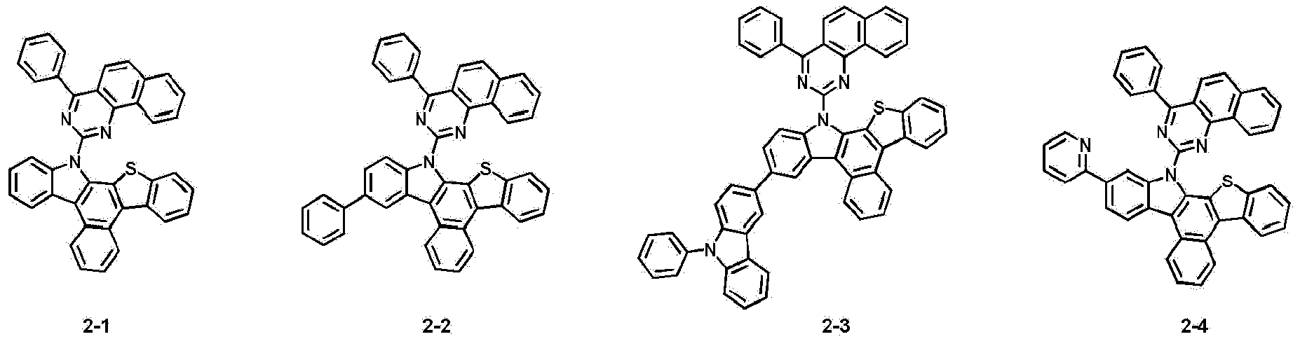


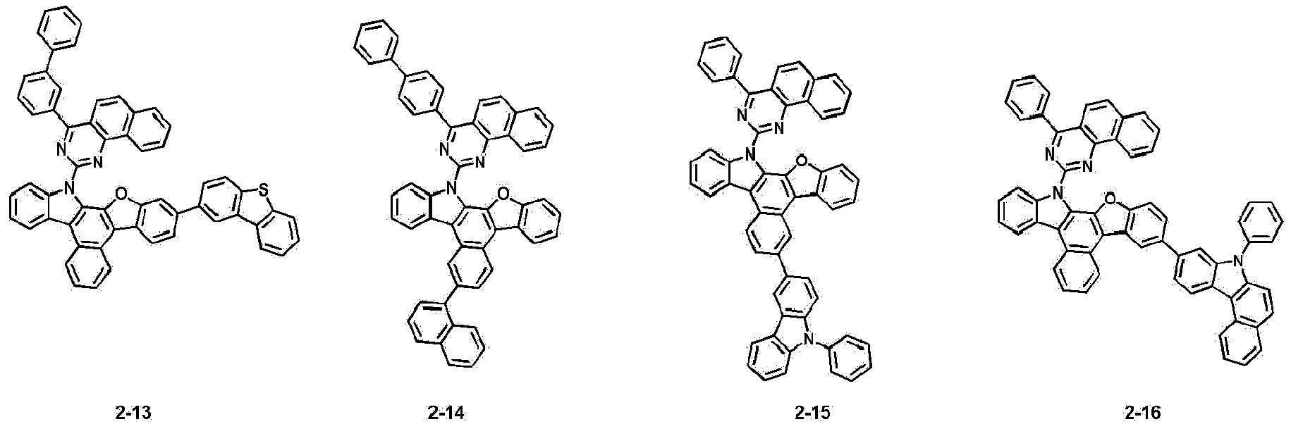


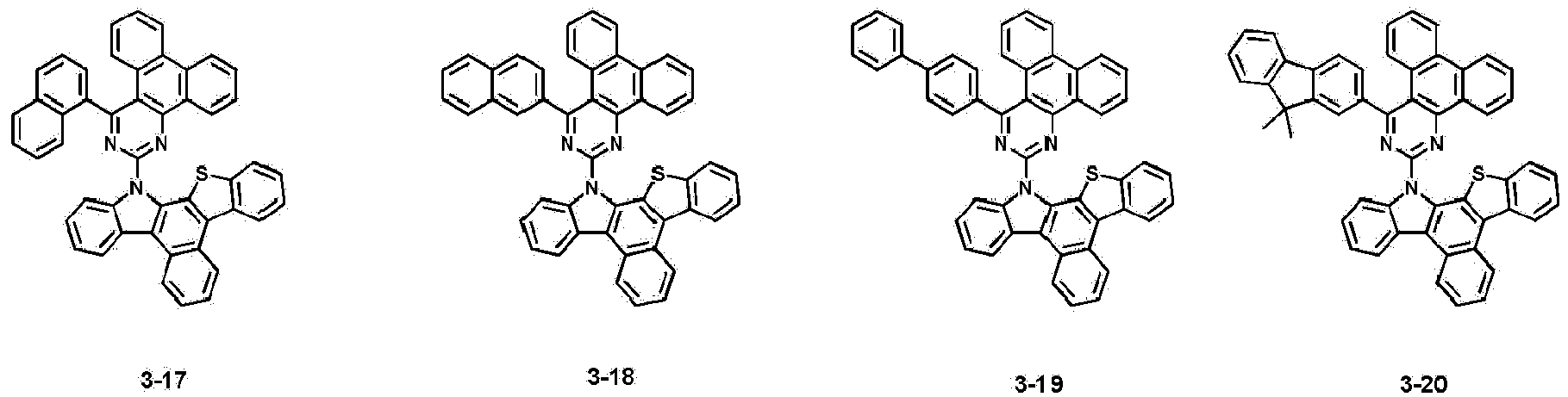


- In another aspect of the present invention, this provides the organic electric element comprising a first electrode, a second electrode, and an organic material layer disposed between the first electrode and the second electrode.
- The organic material layer can be in at least one layer of a hole injection layer, a hole transport layer, a light emitting layer, and an emission-auxiliary layer. And the organic material layer can comprise at least one of the compounds above. Also, the organic material layer can be composed one kind or two or more different kinds of the compounds represented by Formula 1 above.
- Preferably, the light emitting layer of an organic material layer can comprise one kind or two or more different kinds of the compounds represented by Formula 1 above. And the compounds represented by Formula 1 above can comprise as a hose material of a light emitting layer, in particular, a phosphorescent red host material.
- In another aspect of the present invention, when the compound represented by Formula 1 may be used as a host material of a light emitting layer, the following compound represented by Formula 6 can preferably be used as a dopant material. In other words, the compound represented by the following Formula 6 can be contained as the dopant in the light emitting layer of the present invention.


- In Formula 6, each symbol may be defined as follows.
- n may be an integer of 1 to 3.
- A ring and B ring may be independently selected from the group consisting of a C4-C20 cycloalkyl, a C2-C20 heterocyclo alkyl, a C6-C60 aryl, a fluorene, a C2-C60 heteroaryl selected from the group consisting of O, N, S, Si and P, and a fused ring of C3-C60 aliphatic ring and a C6-C60 aromatic ring. Preferably, A ring and B ring may be independently selected from a group consisting of cyclopentene, cyclohexene, benzene, naphthalene, indene, fluorene, pyrrole, imidazole, pyrazole, pyridine, pyrazine, pyrimidine, pyridazine, indole, quinoline, isoquinoline, benzimidazole, furan, benzofuran, thiophene, benzothiophene, thiazole, isothiazole, oxazole, isoxazole, benzothiazole, and benzoxazole.
- X21 to X24 may be independently carbon or nitrogen, preferably, at least one nitrogen.
- R21 and R22 may be independently selected from the group consisting of deuterium, halogen, hydroxyl group, cyano group, nitro group, amino group, amidino group, hydrazine group, hydrazone group, carboxyl group or carboxylic acid salt, phosphoric acid or phosphoric acid salt, -C(=O)Q1 (herein, Q1 is a C1-C10 alkyl group, a C6-C10 aryl group or a C6-C60 aryloxy group), substituted or unsubstituted C1-C60 alkyl group, substituted or unsubstituted C2-C60 alkenyl group, substituted or unsubstituted C2-C60 alkynyl group, substituted or unsubstituted C1-C60 alkoxy group, substituted or unsubstituted C3-C60 cycloalkyl group, substituted or unsubstituted C2-C60 heterocycloalkyl group, substituted or unsubstituted C3-C60 cycloalkenyl group, substituted or unsubstituted C2-C60 heterocycloalkenyl group, substituted or unsubstituted C6-C60 aryl group, substituted or unsubstituted C6-C60 aryloxy group, substituted or unsubstituted C6-C60 arylthio group, and substituted or unsubstituted C2-C60 heteroaryl group,
- a1 and a2 may be independently an integer of 0 to 8. When a1 and a2 may be an integer 2 or more, plural R21s and R22s may be independently the same or different. Preferably, R21 and R22 may be independently selected from the group consisting of deuterium, -F, -Cl, cyano group, nitrogen group, -C(=O)Q1(Q1 is methyl or phenyl group), methyl group, ethyl group, tert-butyl group, methoxy group, tert-butoxy group, and phenyl group. Herein, the methyl group, ethyl group, and tert-butyl group may be respectively substituted by at least one from the group consisting of deuterium, -F, -Cl, cyano group and nitro group. The phenyl group may be substituted at least one from the group consisting of deuterium, -F, -Cl, cyano group, nitro group, -C(=O)Q1(Q1 is methyl or phenyl group), methyl group, tert-butyl group, methoxy group and tert-butoxy group.
- M may be a transition metal having an atomic weight of 40 or more, preferably, M may be Iridium(Ir), Platinum(Pt), Osmium(Os) or Ruthenium (Ru) .
- L may be a mono dentate organic ligand, bidentate organic ligand, tridentate organic ligand or tetradentate organic ligand. m may be an integer of 0 to 4. Preferably, L may be a radical form represented by one of the following formulas.

- When Z11 to Z17 may be C1-C60 alkyl group or C1-C60 alkoxy group, the alkyl group and alkoxy may be optionally substituted by one or more substituents selected from the group consisting of deuterium, halogen, hydroxy group, cyano group and nitro group, and when Z11 to Z17 may be C6-C60 aryl group or C2-C60 heteroaryl group, the aryl group and heteroaryl may be optionally substituted by one or more substituents selected from the group consisting of deterium, halogen, hydroxy group, cyano group, nitro group, C1-C60 alkyl group and C1-C60 alkoxy group.
- The compound represented by Formula 6 above may be represented by any one of the following formulas.

- In Formula 6-1 and 6-2, each symbol may be as defined in Formula 6, these are preferably defined as follows.
- A ring and B ring may be independently selected from the group consisting of cyclopentene, benzene, naphthalene, fluorene, pyridine, pyridazine, quinoline, isoquinoline, benzofuran, benzothiophene, thiazole, isothiazole, and benzoxazole.
- R21 and R22 may be independently selected from the group consisting of deuterium, -F, -Cl, cyano group, nitro group, - C(=O)Q1(here, Q1 is methyl or phenyl group), methyl group, ethyl group, tert-butyl group, methoxy group, tert-butoxy group and phenyl group. Herein, the methyl group, ethyl group, and tert-butyl group may be respectively substituted by at least one from the group consisting of deuterium, -F, -Cl, cyano group and nitro group. The phenyl group may be substituted at least one from the group consisting of deuterium, -F, -Cl, cyano group, nitro group, -C(=O)Q1(Q1 is methyl or phenyl group), methyl group, tert-butyl group, methoxy group and tert-butoxy group. a1 and a2 may be independently an integer of 0 to 2.
- Z11 to Z13 may be independently selected from the group consisting of hydrogen, deuterium, methyl group, ethyl group and tert-butyl group. And, the methyl group, ethyl group and tert-butyl group may be respectively substituted at least one from the group consisting of deuterium, -F, cyano group and nitro group.
- Specifically, the compound represented by Formula 6 above may be represented by one of the following compounds.



- Hereinafter, Synthesis Examples of the compound represented by Formula 1 according to the present invention and Preparation Examples of an organic electric element will be described in detail by way of example. However, the following examples are only for illustrative purposes and are not intended to limit the scope of the invention.
- The final product of the present invention, represented by Formula 1, can be synthesized by reaction between Sub 1 and Sub 2 as illustrated in, but not limited to, the following Reaction Scheme 1.

- Sub 1 of the Reaction Scheme 1 can be synthesized according to, but not limited to, the following Reaction Scheme 2.


-

- A mixture of 5-bromobenzo[b]naphtha[1,2-d]thiophene (50 g, 0.16 mol), bis(pinacolato)diboron (48.65 g, 0.19 mol), KOAc (47 g, 0.48 mol) and PdCl2(dppf) (5.21 g, 4 mol%)in DMF was refluxed for 12 hour at 120°C until completion of the reaction. The reaction solution was cooled to room temperature and extracted with CH2Cl2. The organic layer was washed with water, dried over MgSO4, concentrated in vacuo. The crude product was purified by recrystallization using CH2Cl2 and methanol to give Sub 1-2-1 1 (46 g, 80%).
- A mixture of Sub 1-2-1 (40 g, 0.11 mol), bromo-2-nitrobenzene (26.91 g, 0.13 mol), K2CO3 (46.03 g, 0.33 mol) and Pd(PPh3)4 (5.13 g, 4 mol%) in anhydrous THF and trace amount of water was dissolved and refluxed at 80°C for 12 hour until completion of the reaction. The reaction solution was cooled to room temperature and extracted with CH2Cl2. The organic layer was dried over MgSO4 and concentrated in vacuo. The crude product was purified by column chromatography on silica gel to give Sub 1-4-1 (27.62 g, 70%).
- A solution of Sub 1-4-1 (20 g, 0.05 mol) and triphenylphosphine (44.28 g, 0.17 mol) in o-dichlorobenzene was refluxed for 24 until completion of the reaction. The solvent was removed by vacuum distillation and the crude product was purified by column chromatography on silica gel to give Sub 1(1) (26.68 g, 75%).
-

- Sub 1-2-2(43.0g, 78%) was prepared from 5-bromonaphtho[2,1-b]benzofuran (47.5g, 0.16 mol) as a starting material according to the same way used for Sub 1-2-1 above.
- Sub 1-4-2 (29.3g, 69%) was prepared from Sub 1-2-2 (43g, 0.13 mol) according to the same wau used for Sub 1-4-1 above.
- Sub 1(9) (19.4g, 73%) was prepared from Sub 1-4-2 (29.3g, 0.09 mol) according to the same way used for Sub 1(1) above.
- Examples of Sub 1 compounds include, but are not limited to, the following compounds, and FD-MS data of the compounds are given in Table 1 below.


[Table 1] Compound FD-MS Compound FD-MS Sub 1 (1) m/z=323.08 (C22H13NS=323.41) Sub 1 (2) m/z=399.11 (C28H27NS=399.51) Sub 1 (3) m/z=564.17 (C40H24N2S=564. 70) Sub 1 (4) m/z=400.10 (C27H16N2S=400.49) Sub 1 (5) m/z=505.10 (C34H19NS2=505. 65) Sub 1 (6) m/z=475.14 (C4H21NS=475.60) Sub 1 (7) m/z=554.16 (C37H22N4S=554.66) Sub 1 (8) m/z=564.17 (C40H24N2S=564.70) Sub 1 (9) m/z=307.10(C22H13NO=307.34) Sub 1 (10) m/z=383.13(C28H17NO=383.44) Sub 1 (11) m/z=548.19(C40H24N2O=548.63) Sub 1 (12) m/z=384.13(C27H16N2O=384 4 3) Sub 1 (13) m/z=489.12 (C34H19NOS=489.59) Sub 1 (14) m/z=433.15(C32H19NO=433.50) Sub 1 (15) m/z=548.19(C40H24N2O=548.63) Sub 1 (16) m/z=598.20(C44H26N2O=598.69) - Sub 2 of the Reaction Scheme 1 can be synthesized according to, but not limited to, the following Reaction Scheme 3.

-


- A mixture of Sub 2-1-1 (97 g, 0.56 mol), methyl cyanoacetate (166.5 g, 1.68 mol), KCN (40.1 g, 0.62mol), KOH (62.9 g, 1.12 mol) was added 970mL of DMF and stirred at 60°C for overnight. The solvent was removed by evaporation under vacuum at room temperature. And then to the reaction mixture was added 500 mL of 10% KOH solution(aq.) and refluxed for 1 hour. The reaction solution was cooled to room temperature and extracted with ethylacetate. The organic layer was washed with water, dried over MgSO4, concentrated in vacuo. The crude product was purified by column chromatography and recrystallization with toluene and heptane to give Sub 2-2-1 (54%).
- To a solution of Sub 2-2-1 (25.0 g, 149 mmol)in 200mL of anhydrous THF was stirred and slowly added dropwise phenyl magnesium bromide (3.0 M in Et2O) (87.4 mL, 297 mmol) at 0 °C, and then refluxed for 1 hour. After that, ethyl chloroformate (19.4 g, 179 mmol) was added dropwise to the reaction solution and it was refluxed for 1 hour again. The reaction solution was adjusted weak acid with ammonium chloride solution(aq.), and then, washed with water and heptane to give Sub 2-4-1 (32.4 g, 80%).
- A Sub 2-4-1 (30 g, 110 mmol) was added 80mL of phosphorus oxychloride and refluxed for overnight. And then, the reaction solution was cooled to -20°C and slowly added about 400 mL of water. The crude product was washed with water, methanol and heptane and purified by recrystallization with toluene and heptane to give Sub2(9)(14.1 g, 44%).
-

- A mixture of Sub 2(20) (33.4g, 80 mmol), THF 360 mL, 2-(7-chloro-9,9-dimethyl-9H-fluoren-2-yl)-4,4,5,5-tetramethyl-1,3,2-dioxaborolane (29.8g, 84 mmol), Pd(PPh3)4 (2.8g, 2.4mmol), NaOH (9.6g, 240mmol) and water (180 mL) was refluxed until completion of the reaction. And then, the reaction soluton was extracted with ether and water. The organic layer was dried over MgSO4 and concentrated in vacuo. The crude product was purified by silica gel column chromatography and recrystallization to give Sub 2(28) (38.0g, 78 %).
- Examples of Sub 2 compounds include, but are not limited to, the following compounds, and FD-MS data of the compounds are given in Table 2 below.


[Table 2] Compound FD-MS Compound FD-MS Sub 2 (1) m/z=290.06(C18H11ClN2=290.75) Sub 2 (2) m/z=340.08(C22H13ClN2=340.81) Sub 2 (3) m/z=340.08(C22H13ClN2=340.81) Sub 2 (4) m/z=366.09(C24H15ClN2=366.84) Sub 2 (5) m/z=366.09(C24H15ClN2=366.84) Sub 2 (6) m/z=455.12(C30H18ClN3=455.94) Sub 2 (7) m/z=406.12(C27H19ClN2=406.91) Sub 2 (8) m/z=291.06(C17H10ClN3=291.73) Sub 2 (9) m/z=290.06(C18H11ClN2=290.75) Sub 2 (10) m/z=340.08(C22H13ClN2=340.81) Sub 2 (11) m/z=340.08(C22H13ClN2=340.81) Sub 2 (12) m/z=366.09(C24H15ClN2=366.84) Sub 2 (13) m/z=366.09(C24H15ClN2=366.84) Sub 2 (14) m/z=455.12(C30H18ClN3=455.94) Sub 2 (15) m/z=406.12(C27H19ClN2=406.91) Sub 2 (16) m/z=291.06(C17H10ClN3=291.73) Sub 2 (17) m/z=340.08(C22H13ClN2=340.81) Sub 2 (18) m/z=390.09(C26H15ClN2=390.86) Sub 2 (19) m/z=390.09(C25H15ClN2=390. 86) Sub 2 (20) m/z=416.11(C28H17ClN2=416. 90) Sub 2 (21) m/z=416.11(C28H17ClN2=416. 90) Sub 2 (22) m/z=505.13(C34H20ClN3=506.00) Sub 2 (23) m/z=456.14(C31H21ClN2=456. 96) Sub 2 (24) m/z=341.07(C21H12ClN3=341.79) Sub 2 (25) m/z=366.09(C24H15ClN2=366.84) Sub 2 (26) m/z=492.14(C34H21ClN2=493.00) Sub 2 (27) m/z=548.11(C36H21ClN2S=549.08) Sub 2 (28) m/z=608.20(C43H29ClN2=609.16) -

- Sub 2(1) (15.1g 52.0 mmol), Pd2(dba)3 (2.2 g, 2.4 mmol), P(t-Bu)3 (1 g, 4.73 mmol) and NaOt-Bu (13.6 g, 141.8 mmol) were added to a solution of Sub 1(1) (15.3g, 47.3 mmol) in 500mL of toluene and stirred at 100°C until disappearance of a starting material. The reaction solution was extracted with CH2Cl2 and water and then the organic layer was dried over MgSO4 and concentrated in vacuo. The crude product was purified by silica gel column chromatography and recrystallization to give the product 1-1 (20.8g, 76%).
-

-

-

-

-

-

-

- FD-MS data of the compound 1-1 to 3-20 prepared in the Synthesis Examples of the present invention are given in Table 3 below.
[Table 3] Compound FD-MS Compound FD-MS 1-1 m/z=577.16(C40H23N3S=577.70) 1-2 m/z=653.19(C46H27N3S=653.79) 1-3 m/z=818.25 (C52H34N4S=818. 98) 1-4 m/z=654.19(C45H26N4S=654.78) 1-5 m/z=809.20(C56H31N3S2=810.00) 1-6 m/z=779.24 (C56H33N3S=779.95) 1-7 m/z=858.26(C54H34N6S=859.01) 1-8 m/z=868.27(C62H36N4S=869.04) 1-9 m/z=561.18 (C40H23N3O=561. 63) 1-10 m/z=802.27(C58H34N4O=802.92) 1-11 m/z=918.34(C67H42N4O=919.08) 1-12 m/z=639.21(C44H25N5O=639.70) 1-13 m/z=819.23(C58H33N3OS=819.97) 1-14 m/z=763.26(C56H33N3O=763.88) 1-15 m/z=802.27(C58H34N4O=802.92) 1-16 m/z=852.29(C62H36N4O=852.98) 1-17 m/z=627.18(C44H25N3S=627.75) 1-18 m/z=627.18(C44H25N3S=627.75) 1-19 m/z=658.19(C46H27N3S=653.79) 1-20 m/z=693.22(C49H31N3S=693.86) 2-1 m/z=577.16(C40H23N3S=577.70) 2-2 m/z=653.19(C46H27N3S=653.79) 2-3 m/z=818.25(C52H34N4S=818.98) 2-4 m/z=654.19(C45H26N4S=654.78) 2-5 m/z=809.20 (C56H31N3S2=810.00) 2-6 m/z=779.24 (C56H33N3S=779.95) 2-7 m/z=858.26(C54H34N6S=859.01) 2-8 m/z=868.27(C62H36N4S=869.04) 2-9 m/z=561.18 (C40H23N3O=561. 63) 2-10 m/z=802.27(C58H34N4O=802. 92) 2-11 m/z=918.34(C67H42N4O=919.08) 2-12 m/z=639.21(C44H25N5O=639.70) 2-13 m/z=819.23(C58H33N3OS=819.97) 2-14 m/z=763.26(C56H33N3O=763.88) 2-15 m/z=802.27(C58H34N4O=802.92) 2-16 m/z=852.29(C62H36N4O=852.98) 2-17 m/z=627.18(C44H25N3S=627.75) 2-18 m/z=627.18(C44H25N3S=627.75) 2-19 m/z=658.19(C46H27N3S=653.79) 2-20 m/z=693.22(C49H31N3S=693.86) 3-1 m/z=627.18(C44H25N3S=627.75) 3-2 m/z=703.21(C50H29N3S=703.85) 3-3 m/z=859.21(C60H33N3S2=860.05) 3-4 m/z=704.20(C49H28N4S=704.84) 3-5 m/z=859.21C60H33N3S2=860.05) 3-6 m/z=829.26(C60H35N3S=830.01) 3-7 m/z=908.27(C63H36N6S=909.07) 3-8 m/z=918.28(C66H38N4S=919.10) 3-9 m/z=611.20(C44H25N3O=611. 69) 3-10 m/z=852.29(C62H36N4O=852.98) 3-11 m/z=968.35(C71H44N4O=969.14) 3-12 m/z=689.22(C48H27N5O=689.76) 3-13 m/z=869.25(C62H15N3OS=870.03) 3-14 m/z=813.28(C60H35N3O=813. 94) 3-15 m/z=852.29(C62H36N4O=852.98) 3-16 m/z=902.30(C66H38N4O=903.03) 3-17 m/z=677.19(C48H27N3S=677.81) 3-18 m/z=677.19(C48H27N3S=677.81) 3-19 m/z=703.21(C50H29N3S=703.85) 3-20 m/z=743.24(C53H33N3S=743.91) - An ITO layer (anode) was formed on a glass substrate, and a film of 4,4',4"-tris[2-naphthyl(phenyl)amino]triphenylamine (hereinafter abbreviated as "2-TNATA") was vacuum-deposited on the ITO layer to form a hole injection layer with a thickness of 60nm. Subsequently, N,N'-bis(1-naphthalenyl)-N,N'-bis-phenyl-(1,1'-biphenyl)-4,4'-diamine (hereinafter abbreviated as "NPB") was vacuum-deposited on the hole injection layer to form a hole transfer layer with a thickness of 60nm. Continually, a light emitting layer with a thickness of 30nm was deposited on the hole transfer layer by doping the hole transfer layer with the inventive compound 1-1 as a host material and bis (1-phenylisoquinoline)iridium(III)acetylacetonate (hereinafter abbreviated as (piq)2Ir(acac)) as a dopant material in a weight ratio of 95:5. Next, ((1,1'-biphenyl)-4-olato)bis(2-methyl-8-quinolinolato)aluminum (hereinafter abbreviated as "BAlq") was vacuum-deposited with a thickness of 10nm on the light emitting layer to form a hole blocking layer, a film of tris-(8-hydroxyquinoline)aluminum (hereinafter abbreviated as "Alq3") was formed with a thickness of 40nm to form an electron transport layer. Next, LiF as halogenated alkali metal was deposited with a thickness of 0.2nm on the electron transport layer to form an electron injection layer, and then Al was deposited with a thickness of 150nm on the electron injection layer to form a cathode. In this way, Organic electron emitting diode was completed.
- The OLEDs were manufactured in the same manner as described in Example 1, except that any one of the compounds 1-3 to 3-20 of the present invention in the Table 4 below was used as the host material of the light emitting layer, instead of the inventive compound 1-1.
- OLEDs were manufactured in the same manner as described in Example 1, except that comparative compounds A to C represented below were used as the host material of the light emitting layer, instead of the inventive compound 1-1.

- A forward bias DC voltage was applied to each of the OLEDs manufactured through the Examples 1 to 24 and Comparative Example 1 to 3, and electro-luminescence (EL) characteristics of the OLED were measured by PR-650 (Photo research). Also, T95 life span was measured by life span measuring equipment (Mc science) at reference brightness of 2500cd/m2. Table 4 below shows evaluation results.
[Table 4] Compound Voltage (V) Current Density (mA/cm2) Brightness (cd/m2) Efficiency (cd/A) Lifetime T(90) CIE (x, y) comp.Ex. (1) comp.Com.A 6.7 34.2 2500.0 7.3 75.6 (0.66, 0.32) comp.Ex. (2) comp.Com.B 6.0 23.8 2500.0 10.5 143.6 (0.67, 0.32) comp.Ex. (3) comp.Com.C 5.9 18.0 2500.0 13.9 135.2 (0.66, 0.32) Ex. (1) Com. (1-1) 5.8 10.5 2500.0 23.9 140.5 (0.66, 0.35) Ex. (2) Com. (1-3) 5.7 10.8 2500.0 23.1 140.5 (0.66, 0.35) Ex. (3) Com. (1-9) 5.7 10.9 2500.0 23.0 140.2 (0.66, 0.35) Ex. (4) Com. (1-14) 5.8 11.2 2500.0 22.3 140.1 (0.66, 0.35) Ex. (5) Com. (1-17) 5.9 10.5 2500.0 23.9 140.7 (0.66, 0.35) Ex. (6) Com. (1-18) 5.8 10.4 2500.0 24.0 140.1 (0.66, 0.35) Ex. (7) Com. (1-19) 5.9 10.6 2500.0 23.7 140.7 (0.66, 0.35) Ex. (8) Com. (1-20) 5.7 10.6 2500.0 23.5 140.4 (0.66, 0.35) Ex. (9) Com. (2-1) 5.8 8.9 2500.0 28.0 141.0 (0.66, 0.35) Ex. (10) Com. (2-2) 5.9 9.2 2500.0 27.1 141.1 (0.66, 0.35) Ex. (11) Com. (2-9) 5.8 9.3 2500.0 26.8 141.0 (0.66, 0.35) Ex. (12) Com. (2-11) 5.8 9.5 2500.0 26.3 141.7 (0.66, 0.35) Ex. (13) Com. (2-17) 5.8 9.0 2500.0 27.9 141.6 (0.66, 0.35) Ex. (14) Com. (2-18) 5.7 9.1 2500.0 27.5 141.9 (0.66, 0.35) Ex. (15) Com. (2-19) 5.8 9.0 2500.0 27.8 141.3 (0.66, 0.35) Ex. (16) Com. (2-20) 5.7 9.0 2500.0 27.7 141.5 (0.66, 0.35) Ex. (17) Com. (3-1) 5.8 11.7 2500.0 21.4 138.5 (0.66, 0.35) Ex. (18) Com. (3-6) 5.9 11.9 2500.0 21.0 138.7 (0.66, 0.35) Ex. (19) Com. (3-9) 5.8 12.0 2500.0 20.9 138.1 (0.66, 0.35) Ex. (20) Com. (3-13) 5.8 12.4 2500.0 20.1 138.6 (0.66, 0.35) Ex. (21) Com. (3-17) 5.8 11.5 2500.0 21.6 138.3 (0.66, 0.35) Ex. (22) Com. (3-18) 5.8 11.7 2500.0 21.4 138.2 (0.66, 0.35) Ex. (23) Com. (3-19) 5.9 11.6 2500.0 21.6 138.4 (0.66, 0.35) Ex. (24) Com. (3-20) 5.8 11.5 2500.0 21.8 138.7 (0.66, 0.35) - As shown in the Table 4 above, when the materials for OLEDs of the present invention were used as a phosphorescent host, the driving voltage of the OLEDs could be reduced, and the luminous efficiency and lifespan of the OLEDs could be significantly improved.
- Specifically, the OLEDs using the compounds of the present invention and the Comparative Compounds B and C having the same core with the present invention as a material of the phosphorescent host were found to be significantly improved in driving voltage, luminous efficiency, and lifespan, compared to that of the Comparative Compound A as a common material of the phosphorescent host.
- Also, according to the examples of the present invention and the Comparative Examples 2 and 3, even in the same core, the element properties depended on the substituent bonded to the N of the core. That is, the compounds of the present invention substituted by benzoquinazoline or dibenzoquinazoline were found to be significantly good in the luminous efficiency, compared to that of the Comparative Compound B substituted by quinazoline and the Comparative Compound C substituted by benzotienopyrimidine.
- This is found to be attributed to the fact that, the compounds substituted by benzoquinazoline or dibenzoquinazoline had changed the energy level of the compounds, and as a result, the energy balance were improved, and thus the luminous efficiency were made efficiently in the light emitting layer.
- This is found to be attributed to the fact that, the low driving voltage reduced the thermal damage, and the high molecular weight of the core elicited the high Tg value, leading to an improvement in life span.
- Accordingly, even in the same core, the chemical properties like the energy level of the compound and the element properties like the packing density depended on the substituent bonded to the core, and then the OLED properties depended on the chemical properties and the element properties.
- Although exemplary embodiments of the present invention have been described for illustrative purposes, those skilled in the art will appreciate that various modifications, additions and substitutions are possible, without departing from the scope and spirit of the invention as disclosed in the accompanying claims. Therefore, the embodiment disclosed in the present invention is intended to illustrate the scope of the technical idea of the present invention, and the scope of the present invention is not limited by the embodiment. The scope of the present invention shall be construed on the basis of the accompanying claims, and it shall be construed that all of the technical ideas included within the scope equivalent to the claims belong to the present invention.
Claims (19)
- A compound represented by Formula 1 below:
 Z ring is a C10-C20 aryl group,X is O or S,L1 is selected from the group consisting of a single bond, a C6-C60 arylene group, a fluorenylene group, a C2-C60 heterocyclic group containing at least one heteroatom selected from the group consisting of O, N, S, Si, and P, and a fused ring group of a C3-C60 aliphatic ring and a C6-C60 aromatic ring,Ar1 is selected from the group consisting of a C6-C60 aryl group, a C2-C60 heterocyclic group containing at least one heteroatom selected from the group consisting of O, N, S, Si, and P, a fluorenyl group, and a fused ring group of a C3-C60 aliphatic ring and a C6-C60 aromatic ring,m, n and o are each an integer of 0 to 4, R1, R2 and R3 are independently selected from the group consisting of hydrogen, deuterium, halogen, a C6-C60 aryl group, a fluorenyl group, a C2-C60 heterocyclic group containing at least one heteroatom selected from the group consisting of O, N, S, Si, and P, a fused ring group of a C3-C60 aliphatic ring and a C6-C60 aromatic ring, a C1-C50 alkyl group, a C2-C20alkenyl group, a C2-C20 alkynyl group, a C1-C30 alkoxy group, a C6-C30 aryloxy group, and -L'-N(Ra) (Rb), and each of R1s or R2s or R3s of any adjacent groups is optionally linked together to form at least one fused ring,
 L' is selected from the group consisting of a single bond, a C6-C60 arylene group, a fluorenylene group, a fused ring group of a C3-C60 aliphatic ring and a C6-C60 aromatic ring, and a C2-C60 heterocyclic group containing at least one heteroatom selected from O, N, S, Si, and P,Ra and Rb are independently selected from the group consisting of a C6-C60 aryl group, a fluorenyl group, a fused ring group of a C3-C60 aliphatic ring and a C6-C60 aromatic ring, and a C2-C60 heterocyclic group containing at least one heteroatom selected from O, N, S, Si, and P, andwith the proviso that, the aryl group, heterocyclic group, fluorenyl group, fused ring group, alkyl group, alkenyl group, alkynyl group, alkoxy group, aryloxy group, arylene group, and fluorenylen group are optionally substituted by one or more substituents selected from the group consisting of deuterium, halogen, a silane group, a siloxane group, a boron group, a germanium group, a cyano group, a nitro group, a C1-C20 alkylthio group, a C1-C20 alkoxy group, a C1-C20 alkyl group, a C2-C20 alkenyl group, a C2-C20 alkynyl group, a C6-C20 aryl group, a C6-C20 aryl group substituted by deuterium, a fluorenyl group, a C2-C20 heterocyclic group containing at least one heteroatom selected from the group consisting of O, N, S, Si, and P, a C3-C20 cycloalkyl group, a C7-C20 arylalkyl group, and a C8-C20 arylalkenyl group.
 - The compound as claimed in claim 1, wherein Formula 1 is represented by one of Formula 2 to 4 below:

Ar1, L1, R1 to R3, m, n, o and X are as defined in claim 1. - The compound as claimed in claim 1, wherein Z ring is naphthalene or phenanthrene.
- The compound as claimed in claim 1, wherein Formula 1 is any one of the compounds below:


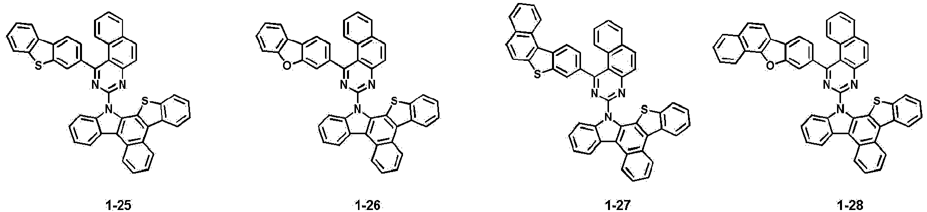


- An organic electric element comprising a first electrode, a second electrode, and an organic material layer disposed between the first electrode and the second electrode, wherein the organic material layer comprises the compound of any one of claims 1 to 4.
- The organic electric element as claimed in claim 5, wherein the compound is comprised in a light emitting layer of the organic material layer.
- The organic electric element as claimed in claim 6, wherein the compound is used as a phosphorescence red host material of the light emitting layer.
- The organic electric element as claimed in claim 7, wherein the host material of the light emitting layer comprises the compound, and a dopant material of the light emitting layer comprises the compound represented by Formula 6 below:
 A ring and B ring are independently selected from the group consisting of a C4-C20 cycloalkyl, a C2-C20 heterocyclo alkyl, a C6-C60 aryl, a fluorene, a C2-C60 heteroaryl selected from a group consisting of O, N, S, Si and P, and a fused ring of C3-C60 aliphatic ring and a C6-C60 aromatic ring,X21 to X24 are independently carbon or nitrogen,R21 and R22 are independently selected from the group consisting of deuterium, halogen, hydroxyl group, cyano group, nitro group, amino group, amidino group, hydrazine group, hydrazone group, carboxyl group or carboxylic acid salt, phosphoric acid or phosphoric acid salt, -C(=O)Q1, substituted or unsubstituted C1-C60 alkyl group, substituted or unsubstituted C2-C60 alkenyl group, substituted or unsubstituted C2-C60 alkynyl group, substituted or unsubstituted C1-C60 alkoxy group, substituted or unsubstituted C3-C60 cycloalkyl group, substituted or unsubstituted C2-C60 heterocycloalkyl group, substituted or unsubstituted C3-C60 cycloalkenyl group, substituted or unsubstituted C2-C60 heterocycloalkenyl group, substituted or unsubstituted C6-C60 aryl group, substituted or unsubstituted C6-C60 aryloxy group, substituted or unsubstituted C6-C60 arylthio group, and substituted or unsubstituted C2-C60 heteroaryl group,wherein Q1 is selected from the group consisting of a C1-C10 alkyl group, a C6-C10 aryl group and a C6-C60 aryloxy group,a1 and a2 are independently an integer of 0 to 8,M is a transition metal having an atomic weight of 40 or more,L is selected from the group consisting of a monodentate organic ligand, bidentate organic ligand, tridentate organic ligand and tetradentate organic ligand,m is an integer of 0 to 4, and,n is an integer of 1 to 3.
 - The organic electric element as claimed in claim 8, wherein, in Formula 6, M is selected from the group of Iridium(Ir), Platinum(Pt), Osmium(Os) and Ruthenium(Ru).
- The organic electric element as claimed in claim 8 or 9, wherein, in Formula 6, at least one of X21 to X24 is nitrogen.
- The organic electric element as claimed in any one of claims 8 to 10, wherein, in Formula 6, A ring and B ring are independently selected from the group consisting of cyclopentene, cyclohexene, benzene, naphthalene, indene, fluorene, pyrrol, imidazole, pyrazole, pyridine, pyrazine, pyrimidine, pyridazine, indole, quinoline, isoquinoline, benzimidazole, furan, benzofuran, thiophene, benzothiophene, thiazole, isothiazole, oxazole, isoxazole, benzothiazole and benzoxazole.
- The organic electric element as claimed in any one of claims 8 to 11, wherein, in Formula 6, R21 and R22 are independently selected from the group consisting of deuterium, -F, -Cl, cyano group, nitro group, -C(=O)Q1, methyl group, ethyl group, tert-butyl group, methoxy group, tert-butoxy group and phenyl group,
wherein the methyl group, ethyl group and tert-butyl group are optionally substituted by one or more substituents selected from the group consisting of deuterium, -F, -Cl, cyano group and nitro group,
wherein the phenyl group is optionally substituted by one or more substituents selected from the group consisting of deuterium, -F, -Cl, cyano group, nitro group, -C(=O)Q1, methyl group, tert-butyl group, methoxy group and tert-butoxy group, and,
wherein Q1 is methyl group or phenyl group. - The organic electric element as claimed in any one of claims 8 to 12, wherein, in Formula 6, L is any one of the following formulas:
 Z11 to Z17 are independently selected from the group consisting of hydrogen, deuterium, halogen, hydroxyl group, cyano group, nitro group, C1-C60 alkyl group, C1-C60 alkoxy group, C6-C60 aryl group and C2-C60 heteroaryl group,wherein the alkyl group and alkoxy group are optionally substituted by one or more substituents selected from the group consisting of deuterium, halogen, hydroxy group, cyano group and nitro group,wherein the aryl group and heteroaryl group are optionally substituted by one or more substituents selected from the group consisting of deuterium, halogen, hydroxy group, cyano group, nitro group, C1-C60 alkyl group and C1-C60 alkoxy group, and,d1 to d4 are independently an integer of 1 to 4.
 - The organic electric element as claimed in any one of claims 8 and 10 to 12, wherein Formula 6 is any one of the following formulas:
 A ring and B ring are independently selected from the group consisting of cyclopentene, benzene, naphthalene, fluoren, pyridine, pyridazine, quinoline, isoquinoline, benzofurane, benzothiophene, thiazole, isothiazole, and benzoxazole,R21 and R22 are independently selected from the group consisting of deuterium, -F, -Cl, cyano group, nitro group, - C(=O)Q1, methyl group, ethyl group, tert-butyl group, methoxy group, tert-butoxy group and phenyl group,a1 and a2 are independently an integer of 0 to 2,Z11 to Z13 are independently selected from the group consisting of hydrogen, deuterium, methyl group, ethyl group and tert-butyl group,wherein the methyl group, ethyl group and tert-butyl group are optionally substituted by one or more substituents selected from the group consisting of deuterium, -F, -Cl, cyano group and nitro group,wherein the phenyl group is optionally substituted by one or more substituents selected from the group consisting of deuterium, -F, -Cl, cyano group, nitro group, -C(=O)Q1, methyl group, tert-butyl group, methoxy group and tert-butoxy group, and,wherein Q1 is methyl group or phenyl group.
 - The organic electric element as claimed in claim 8, wherein the compound represented by Formula 6 is any one of the following compounds:



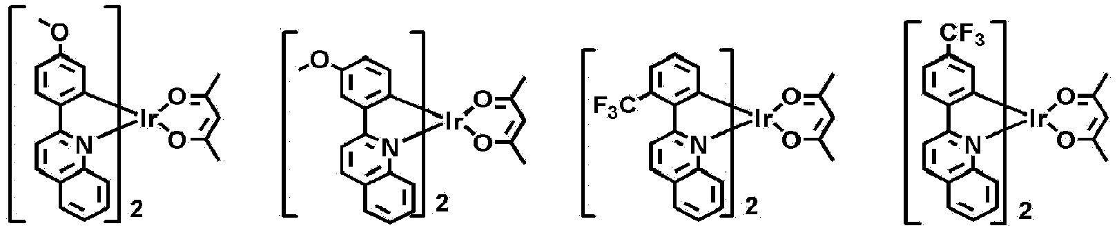

- The organic electric element as claimed in any one of claims 5 to 15, wherein the organic electric element further including at least a layer to improve luminous efficiency which is formed on at least one of the sides the first and second electrodes, which is opposite to the organic material layer.
- The organic electric element as claimed in any one of claims 5 to 16, wherein the organic material layer is formed by any one of the process of spin coating, nozzle printing, inkjet printing, slot coating, dip coating and roll-to-roll.
- An electronic device comprising a display device, which comprises the organic electric element as claimed in any one of claims 5 to 17, and a control unit for driving the display device.
- The electronic device as claimed in claim 18, wherein the organic electric element comprises at least one of an organic light emitting diode, an organic solar cell, an organic photo conductor, an organic transistor, and an element for monochromatic or white illumination.
Applications Claiming Priority (1)
| Application Number | Priority Date | Filing Date | Title |
|---|---|---|---|
| KR1020150122007A KR101604647B1 (en) | 2015-08-28 | 2015-08-28 | Compound for organic electronic element, organic electronic element using the same, and an electronic device thereof |
Publications (2)
| Publication Number | Publication Date |
|---|---|
| EP3135676A1 true EP3135676A1 (en) | 2017-03-01 |
| EP3135676B1 EP3135676B1 (en) | 2018-11-07 |
Family
ID=55272341
Family Applications (1)
| Application Number | Title | Priority Date | Filing Date |
|---|---|---|---|
| EP16153411.0A Active EP3135676B1 (en) | 2015-08-28 | 2016-01-29 | Compound for organic electric element, organic electric element comprising the same, and electronic device thereof |
Country Status (5)
| Country | Link |
|---|---|
| US (2) | US9466803B1 (en) |
| EP (1) | EP3135676B1 (en) |
| JP (1) | JP6236475B2 (en) |
| KR (1) | KR101604647B1 (en) |
| CN (2) | CN107602584B (en) |
Families Citing this family (70)
| Publication number | Priority date | Publication date | Assignee | Title |
|---|---|---|---|---|
| KR102369595B1 (en) * | 2014-12-08 | 2022-03-04 | 삼성디스플레이 주식회사 | Organic light emitting device and display device having the same |
| US11008280B2 (en) * | 2016-04-26 | 2021-05-18 | Duk San Neolux Co., Ltd. | Compound for organic electric element, organic electric element using same, and electronic device comprising same organic electronic element |
| CN106977527B (en) * | 2017-04-25 | 2019-11-08 | 江西冠能光电材料有限公司 | A kind of organic semiconductor compound and the organic electroluminescence device using the compound |
| US12098157B2 (en) | 2017-06-23 | 2024-09-24 | Universal Display Corporation | Organic electroluminescent materials and devices |
| US11228010B2 (en) | 2017-07-26 | 2022-01-18 | Universal Display Corporation | Organic electroluminescent materials and devices |
| US11744142B2 (en) | 2017-08-10 | 2023-08-29 | Universal Display Corporation | Organic electroluminescent materials and devices |
| PL3664925T3 (en) | 2017-08-11 | 2024-06-24 | Gcp Applied Technologies Inc. | Grey water measurement |
| KR102455286B1 (en) * | 2017-11-17 | 2022-10-18 | 덕산네오룩스 주식회사 | Organic electronic element comprising compound for organic electronic element and electronic device thereof |
| US12180230B2 (en) | 2017-11-28 | 2024-12-31 | University Of Southern California | Carbene compounds and organic electroluminescent devices |
| US11937503B2 (en) | 2017-11-30 | 2024-03-19 | Universal Display Corporation | Organic electroluminescent materials and devices |
| US11594305B2 (en) | 2017-12-22 | 2023-02-28 | Verifi Llc | Managing concrete mix design catalogs |
| US11542289B2 (en) | 2018-01-26 | 2023-01-03 | Universal Display Corporation | Organic electroluminescent materials and devices |
| US11165028B2 (en) | 2018-03-12 | 2021-11-02 | Universal Display Corporation | Organic electroluminescent materials and devices |
| US12453279B2 (en) | 2018-08-22 | 2025-10-21 | Universal Display Corporation | Organic electroluminescent materials and devices |
| KR102495276B1 (en) | 2018-11-07 | 2023-02-01 | 삼성에스디아이 주식회사 | Organic optoelectronic device and display device |
| KR102448566B1 (en) | 2018-12-04 | 2022-09-27 | 삼성에스디아이 주식회사 | Organic optoelectronic devices and display devices |
| US11737349B2 (en) | 2018-12-12 | 2023-08-22 | Universal Display Corporation | Organic electroluminescent materials and devices |
| CN109988155A (en) * | 2019-01-16 | 2019-07-09 | 浙江华显光电科技有限公司 | A kind of phosphorescence host compound and its organic electroluminescence device using the compound |
| US11780829B2 (en) | 2019-01-30 | 2023-10-10 | The University Of Southern California | Organic electroluminescent materials and devices |
| US12477890B2 (en) | 2019-02-01 | 2025-11-18 | Universal Display Corporation | Organic electroluminescent materials and devices |
| US12082428B2 (en) | 2019-03-12 | 2024-09-03 | Universal Display Corporation | OLED with triplet emitter and excited state lifetime less than 200 ns |
| JP2020158491A (en) | 2019-03-26 | 2020-10-01 | ユニバーサル ディスプレイ コーポレイション | Organic electroluminescence materials and devices |
| US12281128B2 (en) | 2019-07-30 | 2025-04-22 | Universal Display Corporation | Organic electroluminescent materials and devices |
| US12139501B2 (en) | 2019-08-16 | 2024-11-12 | Universal Display Corporation | Organic electroluminescent materials and devices |
| US20210135130A1 (en) | 2019-11-04 | 2021-05-06 | Universal Display Corporation | Organic electroluminescent materials and devices |
| JP7488091B2 (en) | 2019-11-14 | 2024-05-21 | ユニバーサル ディスプレイ コーポレイション | Organic electroluminescent materials and devices |
| US12538698B2 (en) | 2020-01-06 | 2026-01-27 | Universal Display Corporation | Organic electroluminescent materials and devices |
| US12426495B2 (en) | 2020-01-28 | 2025-09-23 | Universal Display Corporation | Organic electroluminescent materials and devices |
| US12598906B2 (en) | 2020-03-31 | 2026-04-07 | Universal Display Corporation | Organic electroluminescent materials and devices |
| AU2021287242A1 (en) | 2020-06-08 | 2023-02-02 | Gcp Applied Technologies Inc. | Adjusting concrete mixes and mix designs using diagnostic delta data curve |
| EP3937268B1 (en) | 2020-07-10 | 2025-05-07 | Universal Display Corporation | Plasmonic oleds and vertical dipole emitters |
| WO2022072779A1 (en) | 2020-10-02 | 2022-04-07 | Gcp Applied Technologies Inc. | Early strength slag-based cementitious binder |
| US12187748B2 (en) | 2020-11-02 | 2025-01-07 | Universal Display Corporation | Organic electroluminescent materials and devices |
| KR102928151B1 (en) | 2020-11-04 | 2026-02-19 | 덕산네오룩스 주식회사 | Compound for organic electronic element, organic electronic element using the same, and an electronic device thereof |
| US20220158096A1 (en) | 2020-11-16 | 2022-05-19 | Universal Display Corporation | Organic electroluminescent materials and devices |
| US12325717B2 (en) | 2020-11-24 | 2025-06-10 | Universal Display Corporation | Organic electroluminescent materials and devices |
| US20220165967A1 (en) | 2020-11-24 | 2022-05-26 | Universal Display Corporation | Organic electroluminescent materials and devices |
| US12575316B2 (en) | 2021-02-03 | 2026-03-10 | Universal Display Corporation | Organic electroluminescent materials and devices |
| EP4060758A3 (en) | 2021-02-26 | 2023-03-29 | Universal Display Corporation | Organic electroluminescent materials and devices |
| EP4723858A2 (en) | 2021-02-26 | 2026-04-08 | Universal Display Corporation | Organic electroluminescent materials and devices |
| US12606582B2 (en) | 2021-03-05 | 2026-04-21 | Universal Display Corporation | Organic electroluminescent materials and devices |
| US12428599B2 (en) | 2021-03-09 | 2025-09-30 | Universal Display Corporation | Organic electroluminescent materials and devices |
| US20220298190A1 (en) | 2021-03-12 | 2022-09-22 | Universal Display Corporation | Organic electroluminescent materials and devices |
| US12421262B2 (en) | 2021-03-15 | 2025-09-23 | Universal Display Corporation | Organic electroluminescent materials and devices |
| US20220340607A1 (en) | 2021-04-05 | 2022-10-27 | Universal Display Corporation | Organic electroluminescent materials and devices |
| US12480042B2 (en) | 2021-04-09 | 2025-11-25 | Universal Display Corporation | Organic electroluminescent materials and devices |
| EP4075531A1 (en) | 2021-04-13 | 2022-10-19 | Universal Display Corporation | Plasmonic oleds and vertical dipole emitters |
| US20220352478A1 (en) | 2021-04-14 | 2022-11-03 | Universal Display Corporation | Organic eletroluminescent materials and devices |
| US20220407020A1 (en) | 2021-04-23 | 2022-12-22 | Universal Display Corporation | Organic electroluminescent materials and devices |
| US20230006149A1 (en) | 2021-04-23 | 2023-01-05 | Universal Display Corporation | Organic electroluminescent materials and devices |
| US20230133787A1 (en) | 2021-06-08 | 2023-05-04 | University Of Southern California | Molecular Alignment of Homoleptic Iridium Phosphors |
| US12550611B2 (en) | 2021-08-03 | 2026-02-10 | Universal Display Corporation | Organic electroluminescent materials and devices |
| EP4151699A1 (en) | 2021-09-17 | 2023-03-22 | Universal Display Corporation | Organic electroluminescent materials and devices |
| US12473318B2 (en) | 2021-10-08 | 2025-11-18 | Universal Display Corporation | Organic electroluminescent materials and devices |
| US12509628B2 (en) | 2021-12-16 | 2025-12-30 | Universal Display Corporation | Organic electroluminescent materials and devices |
| US20230292592A1 (en) | 2022-03-09 | 2023-09-14 | Universal Display Corporation | Organic electroluminescent materials and devices |
| US20230337516A1 (en) | 2022-04-18 | 2023-10-19 | Universal Display Corporation | Organic electroluminescent materials and devices |
| US20230389421A1 (en) | 2022-05-24 | 2023-11-30 | Universal Display Corporation | Organic electroluminescent materials and devices |
| CN114835663B (en) * | 2022-06-07 | 2025-06-03 | 阜阳欣奕华新材料科技股份有限公司 | A naphthoheteroaryl compound, an organic electroluminescent device and a display device |
| EP4293001A1 (en) | 2022-06-08 | 2023-12-20 | Universal Display Corporation | Organic electroluminescent materials and devices |
| US20240016051A1 (en) | 2022-06-28 | 2024-01-11 | Universal Display Corporation | Organic electroluminescent materials and devices |
| US20240107880A1 (en) | 2022-08-17 | 2024-03-28 | Universal Display Corporation | Organic electroluminescent materials and devices |
| US20240188316A1 (en) | 2022-10-27 | 2024-06-06 | Universal Display Corporation | Organic electroluminescent materials and devices |
| US20240188419A1 (en) | 2022-10-27 | 2024-06-06 | Universal Display Corporation | Organic electroluminescent materials and devices |
| US20240196730A1 (en) | 2022-10-27 | 2024-06-13 | Universal Display Corporation | Organic electroluminescent materials and devices |
| US20240188319A1 (en) | 2022-10-27 | 2024-06-06 | Universal Display Corporation | Organic electroluminescent materials and devices |
| US20240180025A1 (en) | 2022-10-27 | 2024-05-30 | Universal Display Corporation | Organic electroluminescent materials and devices |
| US20240247017A1 (en) | 2022-12-14 | 2024-07-25 | Universal Display Corporation | Organic electroluminescent materials and devices |
| US20250204239A1 (en) | 2023-12-15 | 2025-06-19 | Universal Display Corporation | Organic electroluminescent materials and devices |
| US20250204238A1 (en) | 2023-12-15 | 2025-06-19 | Universal Display Corporation | Organic electroluminscent materials and devices |
Citations (4)
| Publication number | Priority date | Publication date | Assignee | Title |
|---|---|---|---|---|
| KR20140079315A (en) * | 2012-12-18 | 2014-06-26 | 에스에프씨 주식회사 | An electroluminescent compound and an electroluminescent device comprising the same |
| US20140332793A1 (en) * | 2012-01-18 | 2014-11-13 | Duksan High Metal Co., Ltd. | Compound for organic electric element, organic electric element comprising the same and electronic device thereof |
| US20150001511A1 (en) * | 2013-07-01 | 2015-01-01 | Samsung Display Co., Ltd. | Organic light-emitting device |
| WO2015037965A1 (en) * | 2013-09-16 | 2015-03-19 | Rohm And Haas Electronic Materials Korea Ltd. | Novel organic electroluminescent compounds and organic electroluminescent device comprising the same |
Family Cites Families (9)
| Publication number | Priority date | Publication date | Assignee | Title |
|---|---|---|---|---|
| KR101455156B1 (en) * | 2012-11-13 | 2014-10-27 | 덕산하이메탈(주) | Compound for organic electronic element, organic electronic element using the same, and an electronic device thereof |
| KR102098093B1 (en) * | 2012-12-06 | 2020-04-08 | 덕산네오룩스 주식회사 | Compound for organic electronic element, organic electronic element using the same, and an electronic device thereof |
| KR101838833B1 (en) * | 2013-03-27 | 2018-04-26 | 이데미쓰 고산 가부시키가이샤 | Condensed fluoranthene compound, material for organic electroluminescent element using this compound, organic electroluminescent element using this material, and electronic device |
| KR20140126610A (en) * | 2013-04-23 | 2014-10-31 | 삼성디스플레이 주식회사 | Organic light emitting diode |
| KR102251474B1 (en) | 2013-09-16 | 2021-05-17 | 롬엔드하스전자재료코리아유한회사 | Novel organic electroluminescent compounds and organic electroluminescent device comprising the same |
| KR102169449B1 (en) | 2013-10-11 | 2020-10-26 | 에스에프씨 주식회사 | An electroluminescent compound and an electroluminescent device comprising the same |
| KR102249279B1 (en) | 2014-03-25 | 2021-05-07 | 에스에프씨 주식회사 | An organoelectro luminescent compounds and organoelectro luminescent device using the same |
| KR101561566B1 (en) * | 2014-05-28 | 2015-10-27 | 덕산네오룩스 주식회사 | Compound for organic electronic element, organic electronic element using the same, and an electronic device thereof |
| WO2016028110A1 (en) * | 2014-08-20 | 2016-02-25 | Rohm And Haas Electronic Materials Korea Ltd. | A plurality of host materials and an organic electroluminescence device comprising the same |
-
2015
- 2015-08-28 KR KR1020150122007A patent/KR101604647B1/en active Active
- 2015-09-11 US US14/851,719 patent/US9466803B1/en active Active
-
2016
- 2016-01-14 CN CN201710946880.5A patent/CN107602584B/en active Active
- 2016-01-14 CN CN201610023832.4A patent/CN105646522B/en active Active
- 2016-01-21 JP JP2016009513A patent/JP6236475B2/en active Active
- 2016-01-29 EP EP16153411.0A patent/EP3135676B1/en active Active
- 2016-04-26 US US15/138,443 patent/US9530971B1/en active Active
Patent Citations (4)
| Publication number | Priority date | Publication date | Assignee | Title |
|---|---|---|---|---|
| US20140332793A1 (en) * | 2012-01-18 | 2014-11-13 | Duksan High Metal Co., Ltd. | Compound for organic electric element, organic electric element comprising the same and electronic device thereof |
| KR20140079315A (en) * | 2012-12-18 | 2014-06-26 | 에스에프씨 주식회사 | An electroluminescent compound and an electroluminescent device comprising the same |
| US20150001511A1 (en) * | 2013-07-01 | 2015-01-01 | Samsung Display Co., Ltd. | Organic light-emitting device |
| WO2015037965A1 (en) * | 2013-09-16 | 2015-03-19 | Rohm And Haas Electronic Materials Korea Ltd. | Novel organic electroluminescent compounds and organic electroluminescent device comprising the same |
Also Published As
| Publication number | Publication date |
|---|---|
| US9466803B1 (en) | 2016-10-11 |
| JP6236475B2 (en) | 2017-11-22 |
| KR101604647B1 (en) | 2016-03-21 |
| JP2017043596A (en) | 2017-03-02 |
| CN107602584B (en) | 2020-11-03 |
| EP3135676B1 (en) | 2018-11-07 |
| CN105646522B (en) | 2018-04-10 |
| CN105646522A (en) | 2016-06-08 |
| US9530971B1 (en) | 2016-12-27 |
| CN107602584A (en) | 2018-01-19 |
Similar Documents
| Publication | Publication Date | Title |
|---|---|---|
| EP3135676B1 (en) | Compound for organic electric element, organic electric element comprising the same, and electronic device thereof | |
| KR101512059B1 (en) | Compound for organic electric element, organic electric element comprising the same and electronic device thereof | |
| JP5399418B2 (en) | Organic electroluminescence device | |
| KR102637435B1 (en) | Organic electroluminescent materials and devices | |
| JP5421242B2 (en) | Compound for organic electroluminescent device and organic electroluminescent device using the same | |
| KR101614740B1 (en) | Compound for organic electronic element, organic electronic element using the same, and an electronic device thereof | |
| KR102215776B1 (en) | Novel heterocyclic compounds and organic light-emitting diode including the same | |
| KR102098063B1 (en) | Compound for organic electronic element, organic electronic element using the same, and an electronic device thereof | |
| JPWO2011081061A1 (en) | Organic electroluminescence device | |
| KR20140141951A (en) | An organic electronic element using compound for organic electronic element, and an electronic device thereof | |
| KR20150133998A (en) | Compound for organic electronic element, organic electronic element using the same, and an electronic device thereof | |
| KR20190007792A (en) | Compound for organic electronic element, organic electronic element comprising the same, and electronic device thereof | |
| KR20170087691A (en) | Compound for organic electronic element, organic electronic element comprising the same, and electronic device thereof | |
| KR20150042386A (en) | An electroluminescent compound and an electroluminescent device comprising the same | |
| KR20190011463A (en) | Compound for organic electronic element, organic electronic element comprising the same, and electronic device thereof | |
| KR20150042388A (en) | An electroluminescent compound and an electroluminescent device comprising the same | |
| KR20160028737A (en) | An organoelectro luminescent compounds and organoelectro luminescent device using the same | |
| KR20140076519A (en) | An electroluminescent compound and an electroluminescent device comprising the same | |
| KR102249278B1 (en) | Aromatic amine derivative and organic electroluminescent device comprising same | |
| KR102395818B1 (en) | Compound for organic electronic element, organic electronic element using the same, and an electronic device thereof | |
| KR20180032347A (en) | Compound for organic electronic element, organic electronic element comprising the same, and electronic device thereof | |
| KR20150043571A (en) | An electroluminescent compound and an electroluminescent device comprising the same | |
| KR20170016135A (en) | Compound for organic electronic element, organic electronic element using the same, and an electronic device thereof | |
| KR20130142969A (en) | Heterocyclic compounds and organic light-emitting diode including the same | |
| KR20190000162A (en) | Compound for organic electronic element, organic electronic element comprising the same, and electronic device thereof |
Legal Events
| Date | Code | Title | Description |
|---|---|---|---|
| PUAI | Public reference made under article 153(3) epc to a published international application that has entered the european phase |
Free format text: ORIGINAL CODE: 0009012 |
|
| STAA | Information on the status of an ep patent application or granted ep patent |
Free format text: STATUS: REQUEST FOR EXAMINATION WAS MADE |
|
| 17P | Request for examination filed |
Effective date: 20160204 |
|
| AK | Designated contracting states |
Kind code of ref document: A1 Designated state(s): AL AT BE BG CH CY CZ DE DK EE ES FI FR GB GR HR HU IE IS IT LI LT LU LV MC MK MT NL NO PL PT RO RS SE SI SK SM TR |
|
| AX | Request for extension of the european patent |
Extension state: BA ME |
|
| STAA | Information on the status of an ep patent application or granted ep patent |
Free format text: STATUS: EXAMINATION IS IN PROGRESS |
|
| 17Q | First examination report despatched |
Effective date: 20171013 |
|
| GRAP | Despatch of communication of intention to grant a patent |
Free format text: ORIGINAL CODE: EPIDOSNIGR1 |
|
| STAA | Information on the status of an ep patent application or granted ep patent |
Free format text: STATUS: GRANT OF PATENT IS INTENDED |
|
| INTG | Intention to grant announced |
Effective date: 20180305 |
|
| GRAS | Grant fee paid |
Free format text: ORIGINAL CODE: EPIDOSNIGR3 |
|
| GRAJ | Information related to disapproval of communication of intention to grant by the applicant or resumption of examination proceedings by the epo deleted |
Free format text: ORIGINAL CODE: EPIDOSDIGR1 |
|
| GRAL | Information related to payment of fee for publishing/printing deleted |
Free format text: ORIGINAL CODE: EPIDOSDIGR3 |
|
| STAA | Information on the status of an ep patent application or granted ep patent |
Free format text: STATUS: EXAMINATION IS IN PROGRESS |
|
| STAA | Information on the status of an ep patent application or granted ep patent |
Free format text: STATUS: GRANT OF PATENT IS INTENDED |
|
| INTC | Intention to grant announced (deleted) | ||
| RIN1 | Information on inventor provided before grant (corrected) |
Inventor name: LEE, JUNGWOOK Inventor name: LEE, KWANHEE Inventor name: LEE, SUNHEE Inventor name: MUN, SOUNGYUN Inventor name: LEE, BUMSUNG Inventor name: KIM, MIKYUNG Inventor name: PARK, JUNGHWAN |
|
| RAP1 | Party data changed (applicant data changed or rights of an application transferred) |
Owner name: DUK SAN NEOLUX CO., LTD. Owner name: SAMSUNG DISPLAY CO., LTD. |
|
| GRAA | (expected) grant |
Free format text: ORIGINAL CODE: 0009210 |
|
| STAA | Information on the status of an ep patent application or granted ep patent |
Free format text: STATUS: THE PATENT HAS BEEN GRANTED |
|
| AK | Designated contracting states |
Kind code of ref document: B1 Designated state(s): AL AT BE BG CH CY CZ DE DK EE ES FI FR GB GR HR HU IE IS IT LI LT LU LV MC MK MT NL NO PL PT RO RS SE SI SK SM TR |
|
| REG | Reference to a national code |
Ref country code: GB Ref legal event code: FG4D |
|
| REG | Reference to a national code |
Ref country code: CH Ref legal event code: EP Ref country code: AT Ref legal event code: REF Ref document number: 1061927 Country of ref document: AT Kind code of ref document: T Effective date: 20181115 |
|
| REG | Reference to a national code |
Ref country code: DE Ref legal event code: R096 Ref document number: 602016006855 Country of ref document: DE |
|
| REG | Reference to a national code |
Ref country code: IE Ref legal event code: FG4D |
|
| REG | Reference to a national code |
Ref country code: NL Ref legal event code: MP Effective date: 20181107 |
|
| REG | Reference to a national code |
Ref country code: LT Ref legal event code: MG4D |
|
| REG | Reference to a national code |
Ref country code: AT Ref legal event code: MK05 Ref document number: 1061927 Country of ref document: AT Kind code of ref document: T Effective date: 20181107 |
|
| PG25 | Lapsed in a contracting state [announced via postgrant information from national office to epo] |
Ref country code: AT Free format text: LAPSE BECAUSE OF FAILURE TO SUBMIT A TRANSLATION OF THE DESCRIPTION OR TO PAY THE FEE WITHIN THE PRESCRIBED TIME-LIMIT Effective date: 20181107 Ref country code: HR Free format text: LAPSE BECAUSE OF FAILURE TO SUBMIT A TRANSLATION OF THE DESCRIPTION OR TO PAY THE FEE WITHIN THE PRESCRIBED TIME-LIMIT Effective date: 20181107 Ref country code: NO Free format text: LAPSE BECAUSE OF FAILURE TO SUBMIT A TRANSLATION OF THE DESCRIPTION OR TO PAY THE FEE WITHIN THE PRESCRIBED TIME-LIMIT Effective date: 20190207 Ref country code: LV Free format text: LAPSE BECAUSE OF FAILURE TO SUBMIT A TRANSLATION OF THE DESCRIPTION OR TO PAY THE FEE WITHIN THE PRESCRIBED TIME-LIMIT Effective date: 20181107 Ref country code: FI Free format text: LAPSE BECAUSE OF FAILURE TO SUBMIT A TRANSLATION OF THE DESCRIPTION OR TO PAY THE FEE WITHIN THE PRESCRIBED TIME-LIMIT Effective date: 20181107 Ref country code: IS Free format text: LAPSE BECAUSE OF FAILURE TO SUBMIT A TRANSLATION OF THE DESCRIPTION OR TO PAY THE FEE WITHIN THE PRESCRIBED TIME-LIMIT Effective date: 20190307 Ref country code: BG Free format text: LAPSE BECAUSE OF FAILURE TO SUBMIT A TRANSLATION OF THE DESCRIPTION OR TO PAY THE FEE WITHIN THE PRESCRIBED TIME-LIMIT Effective date: 20190207 Ref country code: LT Free format text: LAPSE BECAUSE OF FAILURE TO SUBMIT A TRANSLATION OF THE DESCRIPTION OR TO PAY THE FEE WITHIN THE PRESCRIBED TIME-LIMIT Effective date: 20181107 Ref country code: ES Free format text: LAPSE BECAUSE OF FAILURE TO SUBMIT A TRANSLATION OF THE DESCRIPTION OR TO PAY THE FEE WITHIN THE PRESCRIBED TIME-LIMIT Effective date: 20181107 |
|
| PG25 | Lapsed in a contracting state [announced via postgrant information from national office to epo] |
Ref country code: GR Free format text: LAPSE BECAUSE OF FAILURE TO SUBMIT A TRANSLATION OF THE DESCRIPTION OR TO PAY THE FEE WITHIN THE PRESCRIBED TIME-LIMIT Effective date: 20190208 Ref country code: NL Free format text: LAPSE BECAUSE OF FAILURE TO SUBMIT A TRANSLATION OF THE DESCRIPTION OR TO PAY THE FEE WITHIN THE PRESCRIBED TIME-LIMIT Effective date: 20181107 Ref country code: AL Free format text: LAPSE BECAUSE OF FAILURE TO SUBMIT A TRANSLATION OF THE DESCRIPTION OR TO PAY THE FEE WITHIN THE PRESCRIBED TIME-LIMIT Effective date: 20181107 Ref country code: PT Free format text: LAPSE BECAUSE OF FAILURE TO SUBMIT A TRANSLATION OF THE DESCRIPTION OR TO PAY THE FEE WITHIN THE PRESCRIBED TIME-LIMIT Effective date: 20190307 Ref country code: SE Free format text: LAPSE BECAUSE OF FAILURE TO SUBMIT A TRANSLATION OF THE DESCRIPTION OR TO PAY THE FEE WITHIN THE PRESCRIBED TIME-LIMIT Effective date: 20181107 Ref country code: RS Free format text: LAPSE BECAUSE OF FAILURE TO SUBMIT A TRANSLATION OF THE DESCRIPTION OR TO PAY THE FEE WITHIN THE PRESCRIBED TIME-LIMIT Effective date: 20181107 |
|
| PG25 | Lapsed in a contracting state [announced via postgrant information from national office to epo] |
Ref country code: PL Free format text: LAPSE BECAUSE OF FAILURE TO SUBMIT A TRANSLATION OF THE DESCRIPTION OR TO PAY THE FEE WITHIN THE PRESCRIBED TIME-LIMIT Effective date: 20181107 Ref country code: CZ Free format text: LAPSE BECAUSE OF FAILURE TO SUBMIT A TRANSLATION OF THE DESCRIPTION OR TO PAY THE FEE WITHIN THE PRESCRIBED TIME-LIMIT Effective date: 20181107 Ref country code: IT Free format text: LAPSE BECAUSE OF FAILURE TO SUBMIT A TRANSLATION OF THE DESCRIPTION OR TO PAY THE FEE WITHIN THE PRESCRIBED TIME-LIMIT Effective date: 20181107 Ref country code: DK Free format text: LAPSE BECAUSE OF FAILURE TO SUBMIT A TRANSLATION OF THE DESCRIPTION OR TO PAY THE FEE WITHIN THE PRESCRIBED TIME-LIMIT Effective date: 20181107 |
|
| REG | Reference to a national code |
Ref country code: DE Ref legal event code: R097 Ref document number: 602016006855 Country of ref document: DE |
|
| PG25 | Lapsed in a contracting state [announced via postgrant information from national office to epo] |
Ref country code: MC Free format text: LAPSE BECAUSE OF FAILURE TO SUBMIT A TRANSLATION OF THE DESCRIPTION OR TO PAY THE FEE WITHIN THE PRESCRIBED TIME-LIMIT Effective date: 20181107 Ref country code: RO Free format text: LAPSE BECAUSE OF FAILURE TO SUBMIT A TRANSLATION OF THE DESCRIPTION OR TO PAY THE FEE WITHIN THE PRESCRIBED TIME-LIMIT Effective date: 20181107 Ref country code: SM Free format text: LAPSE BECAUSE OF FAILURE TO SUBMIT A TRANSLATION OF THE DESCRIPTION OR TO PAY THE FEE WITHIN THE PRESCRIBED TIME-LIMIT Effective date: 20181107 Ref country code: EE Free format text: LAPSE BECAUSE OF FAILURE TO SUBMIT A TRANSLATION OF THE DESCRIPTION OR TO PAY THE FEE WITHIN THE PRESCRIBED TIME-LIMIT Effective date: 20181107 Ref country code: SK Free format text: LAPSE BECAUSE OF FAILURE TO SUBMIT A TRANSLATION OF THE DESCRIPTION OR TO PAY THE FEE WITHIN THE PRESCRIBED TIME-LIMIT Effective date: 20181107 |
|
| REG | Reference to a national code |
Ref country code: CH Ref legal event code: PL |
|
| PLBE | No opposition filed within time limit |
Free format text: ORIGINAL CODE: 0009261 |
|
| STAA | Information on the status of an ep patent application or granted ep patent |
Free format text: STATUS: NO OPPOSITION FILED WITHIN TIME LIMIT |
|
| PG25 | Lapsed in a contracting state [announced via postgrant information from national office to epo] |
Ref country code: LU Free format text: LAPSE BECAUSE OF NON-PAYMENT OF DUE FEES Effective date: 20190129 |
|
| 26N | No opposition filed |
Effective date: 20190808 |
|
| REG | Reference to a national code |
Ref country code: BE Ref legal event code: MM Effective date: 20190131 |
|
| REG | Reference to a national code |
Ref country code: IE Ref legal event code: MM4A |
|
| PG25 | Lapsed in a contracting state [announced via postgrant information from national office to epo] |
Ref country code: SI Free format text: LAPSE BECAUSE OF FAILURE TO SUBMIT A TRANSLATION OF THE DESCRIPTION OR TO PAY THE FEE WITHIN THE PRESCRIBED TIME-LIMIT Effective date: 20181107 |
|
| PG25 | Lapsed in a contracting state [announced via postgrant information from national office to epo] |
Ref country code: BE Free format text: LAPSE BECAUSE OF NON-PAYMENT OF DUE FEES Effective date: 20190131 |
|
| PG25 | Lapsed in a contracting state [announced via postgrant information from national office to epo] |
Ref country code: LI Free format text: LAPSE BECAUSE OF NON-PAYMENT OF DUE FEES Effective date: 20190131 Ref country code: CH Free format text: LAPSE BECAUSE OF NON-PAYMENT OF DUE FEES Effective date: 20190131 |
|
| PG25 | Lapsed in a contracting state [announced via postgrant information from national office to epo] |
Ref country code: IE Free format text: LAPSE BECAUSE OF NON-PAYMENT OF DUE FEES Effective date: 20190129 |
|
| PG25 | Lapsed in a contracting state [announced via postgrant information from national office to epo] |
Ref country code: TR Free format text: LAPSE BECAUSE OF FAILURE TO SUBMIT A TRANSLATION OF THE DESCRIPTION OR TO PAY THE FEE WITHIN THE PRESCRIBED TIME-LIMIT Effective date: 20181107 |
|
| PG25 | Lapsed in a contracting state [announced via postgrant information from national office to epo] |
Ref country code: MT Free format text: LAPSE BECAUSE OF NON-PAYMENT OF DUE FEES Effective date: 20190129 |
|
| PG25 | Lapsed in a contracting state [announced via postgrant information from national office to epo] |
Ref country code: CY Free format text: LAPSE BECAUSE OF FAILURE TO SUBMIT A TRANSLATION OF THE DESCRIPTION OR TO PAY THE FEE WITHIN THE PRESCRIBED TIME-LIMIT Effective date: 20181107 |
|
| PG25 | Lapsed in a contracting state [announced via postgrant information from national office to epo] |
Ref country code: HU Free format text: LAPSE BECAUSE OF FAILURE TO SUBMIT A TRANSLATION OF THE DESCRIPTION OR TO PAY THE FEE WITHIN THE PRESCRIBED TIME-LIMIT; INVALID AB INITIO Effective date: 20160129 |
|
| PG25 | Lapsed in a contracting state [announced via postgrant information from national office to epo] |
Ref country code: MK Free format text: LAPSE BECAUSE OF FAILURE TO SUBMIT A TRANSLATION OF THE DESCRIPTION OR TO PAY THE FEE WITHIN THE PRESCRIBED TIME-LIMIT Effective date: 20181107 |
|
| P01 | Opt-out of the competence of the unified patent court (upc) registered |
Effective date: 20230530 |
|
| REG | Reference to a national code |
Ref country code: DE Ref legal event code: R082 Ref document number: 602016006855 Country of ref document: DE Representative=s name: PRUEFER & PARTNER MBB PATENTANWAELTE RECHTSANW, DE |
|
| PGFP | Annual fee paid to national office [announced via postgrant information from national office to epo] |
Ref country code: GB Payment date: 20260126 Year of fee payment: 11 |
|
| PGFP | Annual fee paid to national office [announced via postgrant information from national office to epo] |
Ref country code: DE Payment date: 20260128 Year of fee payment: 11 |
|
| PGFP | Annual fee paid to national office [announced via postgrant information from national office to epo] |
Ref country code: FR Payment date: 20260126 Year of fee payment: 11 |