EP3131205B1 - Rauscharmer mehrwegverstärker und zugehöriges rauscharmes verstärkermodul und empfänger - Google Patents
Rauscharmer mehrwegverstärker und zugehöriges rauscharmes verstärkermodul und empfänger Download PDFInfo
- Publication number
- EP3131205B1 EP3131205B1 EP16178555.5A EP16178555A EP3131205B1 EP 3131205 B1 EP3131205 B1 EP 3131205B1 EP 16178555 A EP16178555 A EP 16178555A EP 3131205 B1 EP3131205 B1 EP 3131205B1
- Authority
- EP
- European Patent Office
- Prior art keywords
- noise
- lna
- signals
- receiver
- generate
- Prior art date
- Legal status (The legal status is an assumption and is not a legal conclusion. Google has not performed a legal analysis and makes no representation as to the accuracy of the status listed.)
- Active
Links
Images


Classifications
-
- H—ELECTRICITY
- H04—ELECTRIC COMMUNICATION TECHNIQUE
- H04B—TRANSMISSION
- H04B1/00—Details of transmission systems, not covered by a single one of groups H04B3/00 - H04B13/00; Details of transmission systems not characterised by the medium used for transmission
- H04B1/06—Receivers
- H04B1/10—Means associated with receiver for limiting or suppressing noise or interference
- H04B1/1081—Reduction of multipath noise
-
- H—ELECTRICITY
- H04—ELECTRIC COMMUNICATION TECHNIQUE
- H04B—TRANSMISSION
- H04B1/00—Details of transmission systems, not covered by a single one of groups H04B3/00 - H04B13/00; Details of transmission systems not characterised by the medium used for transmission
- H04B1/06—Receivers
- H04B1/10—Means associated with receiver for limiting or suppressing noise or interference
- H04B1/12—Neutralising, balancing, or compensation arrangements
-
- H—ELECTRICITY
- H03—ELECTRONIC CIRCUITRY
- H03F—AMPLIFIERS
- H03F1/00—Details of amplifiers with only discharge tubes, only semiconductor devices or only unspecified devices as amplifying elements
- H03F1/26—Modifications of amplifiers to reduce influence of noise generated by amplifying elements
-
- H—ELECTRICITY
- H03—ELECTRONIC CIRCUITRY
- H03F—AMPLIFIERS
- H03F3/00—Amplifiers with only discharge tubes or only semiconductor devices as amplifying elements
- H03F3/189—High-frequency amplifiers, e.g. radio frequency amplifiers
- H03F3/19—High-frequency amplifiers, e.g. radio frequency amplifiers with semiconductor devices only
-
- H—ELECTRICITY
- H03—ELECTRONIC CIRCUITRY
- H03F—AMPLIFIERS
- H03F3/00—Amplifiers with only discharge tubes or only semiconductor devices as amplifying elements
- H03F3/20—Power amplifiers, e.g. Class B amplifiers, Class C amplifiers
- H03F3/21—Power amplifiers, e.g. Class B amplifiers, Class C amplifiers with semiconductor devices only
- H03F3/211—Power amplifiers, e.g. Class B amplifiers, Class C amplifiers with semiconductor devices only using a combination of several amplifiers
-
- H—ELECTRICITY
- H03—ELECTRONIC CIRCUITRY
- H03F—AMPLIFIERS
- H03F3/00—Amplifiers with only discharge tubes or only semiconductor devices as amplifying elements
- H03F3/68—Combinations of amplifiers, e.g. multi-channel amplifiers for stereophonics
-
- H—ELECTRICITY
- H04—ELECTRIC COMMUNICATION TECHNIQUE
- H04B—TRANSMISSION
- H04B1/00—Details of transmission systems, not covered by a single one of groups H04B3/00 - H04B13/00; Details of transmission systems not characterised by the medium used for transmission
- H04B1/005—Details of transmission systems, not covered by a single one of groups H04B3/00 - H04B13/00; Details of transmission systems not characterised by the medium used for transmission adapting radio receivers, transmitters andtransceivers for operation on two or more bands, i.e. frequency ranges
-
- H—ELECTRICITY
- H04—ELECTRIC COMMUNICATION TECHNIQUE
- H04B—TRANSMISSION
- H04B1/00—Details of transmission systems, not covered by a single one of groups H04B3/00 - H04B13/00; Details of transmission systems not characterised by the medium used for transmission
- H04B1/06—Receivers
- H04B1/10—Means associated with receiver for limiting or suppressing noise or interference
- H04B1/12—Neutralising, balancing, or compensation arrangements
- H04B1/123—Neutralising, balancing, or compensation arrangements using adaptive balancing or compensation means
-
- H—ELECTRICITY
- H04—ELECTRIC COMMUNICATION TECHNIQUE
- H04L—TRANSMISSION OF DIGITAL INFORMATION, e.g. TELEGRAPHIC COMMUNICATION
- H04L27/00—Modulated-carrier systems
- H04L27/26—Systems using multi-frequency codes
- H04L27/2601—Multicarrier modulation systems
- H04L27/2647—Arrangements specific to the receiver only
-
- H—ELECTRICITY
- H04—ELECTRIC COMMUNICATION TECHNIQUE
- H04L—TRANSMISSION OF DIGITAL INFORMATION, e.g. TELEGRAPHIC COMMUNICATION
- H04L5/00—Arrangements affording multiple use of the transmission path
- H04L5/0001—Arrangements for dividing the transmission path
- H04L5/0003—Two-dimensional division
- H04L5/0005—Time-frequency
- H04L5/0007—Time-frequency the frequencies being orthogonal, e.g. OFDM(A) or DMT
- H04L5/001—Time-frequency the frequencies being orthogonal, e.g. OFDM(A) or DMT the frequencies being arranged in component carriers
-
- H—ELECTRICITY
- H03—ELECTRONIC CIRCUITRY
- H03F—AMPLIFIERS
- H03F2200/00—Indexing scheme relating to amplifiers
- H03F2200/294—Indexing scheme relating to amplifiers the amplifier being a low noise amplifier [LNA]
-
- H—ELECTRICITY
- H03—ELECTRONIC CIRCUITRY
- H03F—AMPLIFIERS
- H03F2200/00—Indexing scheme relating to amplifiers
- H03F2200/318—A matching circuit being used as coupling element between two amplifying stages
-
- H—ELECTRICITY
- H03—ELECTRONIC CIRCUITRY
- H03F—AMPLIFIERS
- H03F2200/00—Indexing scheme relating to amplifiers
- H03F2200/372—Noise reduction and elimination in amplifier
-
- H—ELECTRICITY
- H03—ELECTRONIC CIRCUITRY
- H03F—AMPLIFIERS
- H03F2200/00—Indexing scheme relating to amplifiers
- H03F2200/451—Indexing scheme relating to amplifiers the amplifier being a radio frequency amplifier
Definitions
- carrier aggregation is used in order to increase the bandwidth, where the carrier aggregation comprises several operation modes such as intra-band continuous/non-contiguous carrier aggregation and inter-band carrier aggregation. Therefore, a receiver is required to support all the carrier aggregation operation modes. The receiver usually suffers from noise degradation when operating in some operation modes such as the non-contiguous carrier aggregation mode, a noise-cancellation technique is a good candidate to improve the performance by performing the noise cancellation upon the signal. Hence, a circuit design to satisfy the aforementioned requirements is an important topic.
- US2010/0261438A1 discloses a low-noise amplifier according to the preamble portion of claim 1.
- US2014/0170999A1 discloses techniques for simultaneously receiving multiple transmitted signals with independent gain control, wherein an apparatus includes a low noise amplifier.
- US2015/0180694A1 discloses a radio frequency circuit for intra-band and inter-band carrier aggregation, wherein the radio frequency circuit includes a low noise amplifier which has multiple separate input stages and multiple separate output stages.
- US2014/0134959A1 discloses an apparatus including a low noise amplifier and an interface circuit.
- US2013/0057346A1 discloses an amplifier comprising an impedance matching stage, a feedback circuit, and a gain stage.
- US2014/0355728A1 discloses a receiver front end circuit that includes a low-noise amplifier.
- RF radio frequency
- the receiver comprises a low-noise amplifier (LNA) module comprising a plurality of LNAs, wherein the LNAs are arranged to receive input signals from a plurality of input ports, respectively, and each of the LNAs generates and outputs a plurality of noise-cancelled signals at a plurality of output terminals of the LNA module.
- LNA low-noise amplifier
- a LNA module of a receiver comprises a plurality of LNAs, wherein the LNAs are arranged to receive input signals from a plurality of input ports, respectively, and each of the LNAs generates and outputs a plurality of noise-cancelled signals to a plurality of output terminals of the LNA module.
- a LNA for receiving an input signal to generate a plurality of noise-cancelled signals.
- the LNA comprises a plurality of main amplifiers, a matching circuit and a plurality of combiners.
- Each of the main amplifiers is selectively enabled to receive the input signal to generate an amplified signal;
- the matching circuit is arranged for providing input matching and further receiving the input signal.
- the plurality of combiners are respectively coupled to the main amplifiers, wherein each of the combiners is arranged to combine the corresponding amplified signal, if any, with an output of the matching circuit to generate the corresponding noise-cancelled signal.
- FIG. 1 is a diagram illustrating a receiver 100 according to one embodiment of the present invention.
- the receiver 100 comprises a plurality of RF input ports 110_1-110_M, a LNA module 120 and mixers 130, where the LNA module 120 comprises a plurality of LNAs 124_1-124_M and a plurality of output terminals 122_1-122_N.
- the quantity of the LNAs and the output terminals of the LNA module 120 i.e. values of M and N
- M may be 8 while N may be 3.
- the RF input ports 110_1-110_M are arranged to receive input signals from an antenna front-end module, respectively, where the input signals may belong to different standards and/or different specifications.
- the LNAs 124_1-124_M are arranged to receive the input signals from the RF input ports 110_1-110_M, respectively, to generate a plurality of noise-cancelled signals to the output terminals 122_1-122_N. Then, the mixers 130 mix the noise-cancelled signals with local oscillation signals to generate a plurality of down-converted signals, respectively, to the following base-band circuits.
- each of the LNAs 124_1-124_M is allowed to generate N noise-cancelled signals to the output terminals 122_1-122_N; and in practice, a portion of the LNAs is/are controlled to generate one or more noise-cancelled signals, and any one output terminals of the LNA module receives the corresponding noise-cancelled signal from only one of the LNAs 124_1-124_M.
- the LNA module 120 can be regarded as a RF multiplexer, which can pass the selected input signals to the mixers 130 by controlling the LNAs 124_1-124_M.
- FIG. 2 is a diagram illustrating a LNA 200 according to one embodiment of the present invention, where the LNA 200 can be used in at least a portion of the LNA 124_1-124_M shown in FIG. 1 .
- the LNA 200 comprises a plurality of main amplifiers 210_1-210_N, a matching circuit 220 and a plurality of combiner 230_1-230_N, where the matching circuit 220 comprises a matching amplifier 222, a variable resistor 224 positioned in a feedback path of the matching amplifier 220 and a plurality of buffers 226_1-226_N (e.g. unity gain amplifiers, source followers).
- the matching circuit 220 comprises a matching amplifier 222, a variable resistor 224 positioned in a feedback path of the matching amplifier 220 and a plurality of buffers 226_1-226_N (e.g. unity gain amplifiers, source followers).
- each of the main amplifiers 210_1-210_N is selectively enabled to receive an input signal Vin from one of the RF input ports 110_1-110_M to generate an amplified signal.
- the matching amplifier 220 is used to provide input matching (e.g. 50 ohm) and further to receive the input signal Vin, and the buffers 226_1-226_N buffer an output of the matching amplifier 222 to generate a plurality of outputs of the matching amplifier 220.
- the combiners 230_1-230_N combine the amplified signals and the outputs of the matching circuit 200 to generate a plurality of noise-cancelled-signals Vncl-VncN to the output terminals 122_1-122_N, respectively.
- the LNA 200 when the LNA 200 is controlled to pass the input signal Vin to all the output terminals 122_1-122_N of the LNA module 120, all the main amplifiers 210_1-210_N are enabled to generate N amplified signals, and all the buffers 226_1-226_N are enabled to generate N outputs (i.e. with inverted noise signal), and the combiners 230_1-230_N combine the N amplified signals and N outputs of the buffers 226_1-226_N to generate the noise-cancelled signals Vncl-VncN, respectively.
- the main amplifier 210_1 When the LNA 200 is controlled to pass the input signal Vin to one output terminal 122_1 only, the main amplifier 210_1 is enabled to generate the amplified signal while the other main amplifiers are disabled, and the buffer 226_1 is enabled to generate the output (i.e. with inverted noise signal) while the other buffers are disabled, and the combiner 230_1 combines the amplified signal of the main amplifier 210_1 and the output of the buffer 226_1 to generate the noise-cancelled signals Vnc1 to the output terminal 122_1.
- the main amplifiers 210_1 and 210_2 are enabled to generate the amplified signals while the other main amplifiers are disabled, and the buffers 226_1 and 226_2 are enabled to generate the outputs (i.e. with inverted noise signal) while the other buffers are disabled, and the combiners 230_1 and 230_2 combine the amplified signals of the main amplifiers 210_1 and 210_2 and the outputs of the buffers 226_1 and 226_2 to generate the noise-cancelled signals Vnc1 and Vnc2, respectively.
- the LNA 200 can flexibly pass the input signal Vin to one or more of the output terminals 122_1-122_N for further processing (i.e. down conversion performed by the mixers 130), or not pass the input signal Vin to any one of the output terminals 122_1-122_N. Therefore, referring back to FIG. 1 , the LNA module 120 can selectively pass any input signal to any output terminal by controlling internal elements of the LNAs 124_1-124_M, that is, the receiver 100 can support many different signal modes such as the intra-band continuous/non-contiguous carrier aggregation and inter-band carrier aggregation for LTE.
- the existence of the matching circuit 220 may induce noise to the input signal Vin and the amplified signals of the main amplifiers 210_1-210_N, therefore, the design of the matching amplifier 222 with the variable resistor 224 can generate the output whose noise is opposite to the noise carried on the amplified signals (i.e. the phases of the noises on the output of the matching amplifier 222 and the amplified signals of the main amplifiers 210_1-210_N are inverted), thereby the noise caused by the matching circuit 220 can be removed from the amplified signals by using the combiners 230_1-230_N to generate the noise-cancelled signals Vnc1-VncN.
- the aforementioned amplified signals of the main amplifiers 210_1-210_N and the outputs of the matching circuit 220 can be voltage signals or current signals.
- the combiners 230_1-230_N can be implemented by a voltage summer amplifier; and when the amplified signals are current signals, the combiners 230_1-230_N can be implemented by a node or a current summer for summing the amplified signal and the corresponding output of the matching circuit 220.
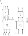
- FIG. 3 shows that the receiver 100 further comprises a LNA module 320 and mixers 330, where the LNA module 120 and the mixers 330 are positioned in different chips.
- the output terminal 122_N of the LNA module 120 is connected to an input terminal of the LNA module 320, and the noise-cancelled signal VncN of the LNA module 120 is selectively forwarded to the other LNA module 320 or not.
- the output terminal 122_N of the LNA module 120 can be directly connected to an input terminal of mixers 330, and the noise-cancelled signal VncN of the LNA module 120 is selectively forwarded to the other mixers 330 or not.
- the mixers 130 will not process the noise-cancelled signal VncN, and the noise-cancelled signal VncN is forwarded to the LNA module 320 or the mixers 330 on another chip.
- the LNA module 320 amplifies or directly passes the noise-cancelled signal VncN to the mixers 330 to generate the down-converted signal to the following base-band circuit.
- FIG. 5 is a diagram illustrating detail structure of the receiver 100 according to one embodiment of the present invention, where the quantity of the LNAs is eight and the quantity of output terminals of the LNA module 120 is three, that is, M is equal to 8 and N is equal to 3. As shown in FIG.
- only one of the main amplifiers 210_1 of the LNAs 124_1-124_8 is controlled to generate the amplified signal to a current buffer 410, and the combiner 230_1 combines the amplified signal from the current buffer 410 and the output of the matching circuit 220 to generate the noise-cancelled signal; then, by switching on one of switches SW1 and SW2, the noise-cancelled signal is inputted to the mixer 130_1 via the switch SW2 or via the inductor L2 and the switch SW1, wherein the inductor L2 serves as a gain booster by means of series inductor peaking technique when the switch SW1 is on; then, the mixer 130_1 mixes the noise-cancelled signal with a local oscillation signal LO1 to generate a down-converted signal.
- the combiner 230_2 combines the amplified signal from the current buffer 420 and the output of the matching circuit 220 to generate the noise-cancelled signal; then, by switching on one of switches SW3 and SW4, the noise-cancelled signal is inputted to the mixer 130_2 via the switch SW4 or via the inductor L4 and the switch SW3, wherein the inductor L4 serves as a gain booster when the switch SW3 is on; then, the mixer 130_2 mixes the noise-cancelled signal with a local oscillation signal LO2 to generate a down-converted signal.
- the combiner 230_3 combines the amplified signal from the current buffer 430 and the output of the matching circuit 220 to generate the noise-cancelled signal; then, by switching on one of switches SW5 and SW6, the noise-cancelled signal is inputted to the mixer 130_3 via the switch SW6 or via the inductor L6 and the switch SW5, wherein the inductor L6 serves as a gain booster when the switch SW5 is on; then, the mixer 130_3 mixes the noise-cancelled signal with a local oscillation signal LO3 to generate a down-converted signal, or the noise-cancelled signal is forwarded to another chip. It should be noted that the present invention re-uses a portion of LNA spiral inductor load as series peaking inductor (L2, L4, L6) to save chip area.
- the LNA module can flexibly amplify selected RF input signals and pass the amplified RF input signals into following mixers, and a plurality of noise-cancellation path is used to cancel some portion of noise upon the amplified RF signals.
- the receiver can support all different carrier aggregation modes and the signal quality of all RF signal paths can be further improved.
Landscapes
- Engineering & Computer Science (AREA)
- Signal Processing (AREA)
- Computer Networks & Wireless Communication (AREA)
- Power Engineering (AREA)
- Amplifiers (AREA)
Claims (10)
- Rauscharmer Verstärker (200), auch als LNA bezeichnet, zum Empfangen eines Eingangssignals, um eine Mehrzahl von rauschunterdrückten Signalen zu generieren, aufweisend:eine Mehrzahl von Hauptverstärkern (210_1 - 210_N), wobei jedem der Hauptverstärker (210_1 - 210_N) selektiv ermöglicht wird, das Eingangssignal zu empfangen, um ein verstärktes Signal zu generieren;gekennzeichnet durch:eine Anpassschaltung (220) für ein Bereitstellen einer Eingangsanpassung und weiter ein Empfangen des Eingangssignals; undeine Mehrzahl von Kombinatoren (230_1 - 230_N), die jeweils mit den Hauptverstärkern (210_1 - 210_N) verbunden sind, wobei jeder der Kombinatoren (230_1 - 230_N) eingerichtet ist, das korrespondierende verstärkte Signal, soweit vorhanden, mit einem Ausgangssignal der Anpassschaltung (220) zu kombinieren, um das korrespondierende rauschunterdrückte Signal zu generieren,wobei die Anpassschaltung (220) aufweist:einen Anpassverstärker (222) zum Empfangen des Eingangssignals; undeinen Widerstand (224), der in einem Rückkopplungspfad des Anpassverstärkers (222) angeordnet ist, undeine Mehrzahl von Pufferverstärkern (226_1 - 226_N) zum Empfangen eines Ausgangssignals des Anpassverstärkers (222), um jeweils eine Mehrzahl von Ausgangssignalen der Anpassschaltung (220) an die Kombinatoren (230_1 - 230_N) zu generieren.
- Rauscharmes Verstärker- (LNA-) Modul (120) eines Empfängers (100), gekennzeichnet durch:
eine Mehrzahl von LNAs (124_1 - 124_M) gemäß Anspruch 1, wobei die LNAs (124_1 - 124_M) eingerichtet sind, Eingangssignale jeweils von einer Mehrzahl von Eingangsanschlüssen (110_1 - 110_M) zu empfangen, und jeder der LNAs (124_1 - 124_M) eingerichtet ist, eine Mehrzahl von rauschunterdrückten Signalen an einer Mehrzahl von Ausgangsanschlüssen (122_1 - 122_N) des LNA-Moduls zu generieren und auszugeben. - Empfänger (100), gekennzeichnet durch Aufweisen des rauscharmen Verstärker-(LNA-) Moduls (120) gemäß Anspruch 2.
- Empfänger (100) gemäß Anspruch 3, dadurch gekennzeichnet, dass ein erster LNA (124_1) der LNAs (124_1 - 124_M) eingerichtet ist, gesteuert zu werden, um eine Mehrzahl von ersten rauschunterdrückten Signalen zu generieren, und die Mehrzahl von ersten rauschunterdrückten Signalen an der Mehrzahl von Ausgangsanschlüssen (122_1 - 122_N) des LNA-Moduls (120) auszugeben.
- Empfänger (100) gemäß Anspruch 3, dadurch gekennzeichnet, dass ein zweiter LNA (124_2) der LNAs (124_1 - 124_M) eingerichtet ist, gesteuert zu werden, eine Mehrzahl von zweiten rauschunterdrückten Signalen zu generieren, und die Mehrzahl von zweiten rauschunterdrückten Signalen an der Mehrzahl von Ausgangsanschlüssen (122_1 - 122_N) des LNA-Moduls (120) auszugeben.
- Empfänger (100) gemäß Anspruch 5, dadurch gekennzeichnet, dass ein erster Ausgangsanschluss (122_1) der Mehrzahl von Ausgangsanschlüssen (122_1 - 122_N) eingerichtet ist, mindestens eins der ersten rauschunterdrückten Signale und mindestens eins der zweiten rauschunterdrückten Signale zu empfangen.
- Empfänger (100) gemäß Anspruch 3, dadurch gekennzeichnet, dass das LNA-Modul (120) in einem Chip angeordnet ist und eingerichtet ist, ein oder mehrere rauschunterdrückte Signale zu einem anderen Chip (330) weiterzuleiten.
- Empfänger (100) gemäß Anspruch 3, dadurch gekennzeichnet, dass er weiter aufweist:
eine Mehrzahl von Mischern (130), die mit den Ausgangsanschlüssen (122_1 - 122_N) des LNA-Moduls (120) verbunden sind, zum Mischen der rauschunterdrückten Signale mit lokalen Oszillationssignalen, um jeweils eine Mehrzahl von abwärtskonvertierten Signalen zu generieren. - Empfänger (100) gemäß Anspruch 8, dadurch gekennzeichnet, dass das LNA-Modul (120) in einem Chip angeordnet ist und eingerichtet ist, ein oder mehrere rauschunterdrückte Signale zu einem anderen Chip (330) weiterzuleiten.
- Empfänger (100) gemäß Anspruch 3, dadurch gekennzeichnet, dass eine Anzahl der LNAs (124_1 - 124_M) größer ist als eine Anzahl der Ausgangsanschlüsse (122_1 - 122_N) des LNA-Moduls (120).
Applications Claiming Priority (2)
| Application Number | Priority Date | Filing Date | Title |
|---|---|---|---|
| US201562203493P | 2015-08-11 | 2015-08-11 | |
| US15/199,948 US9859930B2 (en) | 2015-08-11 | 2016-06-30 | Multi-path low-noise amplifier and associated low-noise amplifier module and receiver |
Publications (3)
| Publication Number | Publication Date |
|---|---|
| EP3131205A2 EP3131205A2 (de) | 2017-02-15 |
| EP3131205A3 EP3131205A3 (de) | 2017-03-22 |
| EP3131205B1 true EP3131205B1 (de) | 2018-10-03 |
Family
ID=56372824
Family Applications (1)
| Application Number | Title | Priority Date | Filing Date |
|---|---|---|---|
| EP16178555.5A Active EP3131205B1 (de) | 2015-08-11 | 2016-07-08 | Rauscharmer mehrwegverstärker und zugehöriges rauscharmes verstärkermodul und empfänger |
Country Status (3)
| Country | Link |
|---|---|
| US (1) | US9859930B2 (de) |
| EP (1) | EP3131205B1 (de) |
| CN (1) | CN106452468B (de) |
Families Citing this family (5)
| Publication number | Priority date | Publication date | Assignee | Title |
|---|---|---|---|---|
| US10008987B1 (en) * | 2016-12-16 | 2018-06-26 | Qualcomm Incorporated | Switch and matching noise cancelling for switch low noise amplifier |
| US10305458B1 (en) | 2018-03-27 | 2019-05-28 | Qualcomm Incorporated | Repetitive noise cancelation |
| US10567017B2 (en) | 2018-06-19 | 2020-02-18 | Mediatek Inc. | Saw-less design in low supply voltage and single-ended receiver and associated signal processing method |
| US10797738B2 (en) | 2018-10-26 | 2020-10-06 | Analog Devices, Inc. | Segmented receiver for wireless communications |
| KR102653890B1 (ko) | 2019-10-18 | 2024-04-02 | 삼성전자주식회사 | 반송파 집성을 지원하는 rfic 및 이를 포함하는 무선 통신 장치 |
Family Cites Families (11)
| Publication number | Priority date | Publication date | Assignee | Title |
|---|---|---|---|---|
| US7693674B2 (en) * | 2005-05-20 | 2010-04-06 | Omniphase Research Laboratories, Inc. | Low-noise source |
| KR100824783B1 (ko) * | 2006-10-17 | 2008-04-24 | 삼성전자주식회사 | 다중 대역용 저잡음 증폭기 및 다중 대역용 무선 신호수신기 |
| US8412142B2 (en) | 2009-04-09 | 2013-04-02 | Broadcom Corporation | Multiple frequency band information signal universal front end with adjustable ADC(s) |
| GB2486515B (en) | 2011-09-02 | 2012-11-14 | Renesas Mobile Corp | Apparatus and method for low noise amplification |
| US8503967B2 (en) | 2011-08-04 | 2013-08-06 | Mediatek Inc. | Amplifier and associated receiver |
| US9300420B2 (en) | 2012-09-11 | 2016-03-29 | Qualcomm Incorporated | Carrier aggregation receiver architecture |
| US9048928B2 (en) | 2012-11-13 | 2015-06-02 | Qualcomm Incorporated | Expandable transceivers and receivers |
| US9548709B2 (en) | 2012-12-19 | 2017-01-17 | Qualcomm Incorporated | Independent gain control for multiple receive circuits concurrently processing different transmitted signals |
| US9025709B2 (en) * | 2013-05-30 | 2015-05-05 | Mediatek Inc. | Receiver front-end circuit, communication unit and method therefor |
| US20150180694A1 (en) | 2013-12-19 | 2015-06-25 | Nvidia Corporation | Radio frequency circuit for intra-band and inter-band carrier aggregation |
| US9515749B2 (en) * | 2015-05-07 | 2016-12-06 | Qualcomm Incorporated | Low noise amplifier module with output coupler |
-
2016
- 2016-06-30 US US15/199,948 patent/US9859930B2/en active Active
- 2016-07-08 EP EP16178555.5A patent/EP3131205B1/de active Active
- 2016-08-10 CN CN201610651485.XA patent/CN106452468B/zh active Active
Non-Patent Citations (1)
| Title |
|---|
| None * |
Also Published As
| Publication number | Publication date |
|---|---|
| CN106452468A (zh) | 2017-02-22 |
| EP3131205A3 (de) | 2017-03-22 |
| CN106452468B (zh) | 2019-08-02 |
| EP3131205A2 (de) | 2017-02-15 |
| US20170047956A1 (en) | 2017-02-16 |
| US9859930B2 (en) | 2018-01-02 |
Similar Documents
| Publication | Publication Date | Title |
|---|---|---|
| JP5951906B2 (ja) | 出力ごとに独立した利得制御を備える単一入力多出力増幅器 | |
| EP3131205B1 (de) | Rauscharmer mehrwegverstärker und zugehöriges rauscharmes verstärkermodul und empfänger | |
| JP6224293B1 (ja) | マルチバンド受信機のための2段低雑音増幅器 | |
| US10848105B2 (en) | Power amplification module | |
| US9271239B2 (en) | Current-efficient low noise amplifier (LNA) | |
| US10483928B2 (en) | Power amplification module | |
| US11265037B2 (en) | Radio frequency circuit and communication device | |
| CN106105027B (zh) | 用于载波聚合放大器的杂散信号的减轻 | |
| EP4507258A2 (de) | Multiplexmodule für trägeraggregationsempfänger | |
| US20140018026A1 (en) | Receiver, Method and Mobile Communication Device | |
| US7253688B2 (en) | Input matching circuit for multiband low noise amplifier | |
| US12574055B2 (en) | Radio-frequency circuit | |
| EP3219016B1 (de) | Empfänger-frontend-architektur zur intraband-trägeraggregation | |
| US10135398B2 (en) | Power amplification module | |
| US10826450B2 (en) | Hybrid concurrent and switched dual-band low noise amplifier | |
| US10340860B1 (en) | Multi-mode low noise amplifier | |
| US12057901B2 (en) | Radio architecture for switching among transmission paths | |
| US12009564B2 (en) | Multi mode phased array element | |
| US10756686B2 (en) | Band sharing technique of receiver | |
| US20050181751A1 (en) | Power amplifier arrangement having an antenna, and a method for amplification and emission of a signal |
Legal Events
| Date | Code | Title | Description |
|---|---|---|---|
| PUAI | Public reference made under article 153(3) epc to a published international application that has entered the european phase |
Free format text: ORIGINAL CODE: 0009012 |
|
| STAA | Information on the status of an ep patent application or granted ep patent |
Free format text: STATUS: THE APPLICATION HAS BEEN PUBLISHED |
|
| AK | Designated contracting states |
Kind code of ref document: A2 Designated state(s): AL AT BE BG CH CY CZ DE DK EE ES FI FR GB GR HR HU IE IS IT LI LT LU LV MC MK MT NL NO PL PT RO RS SE SI SK SM TR |
|
| AX | Request for extension of the european patent |
Extension state: BA ME |
|
| PUAL | Search report despatched |
Free format text: ORIGINAL CODE: 0009013 |
|
| AK | Designated contracting states |
Kind code of ref document: A3 Designated state(s): AL AT BE BG CH CY CZ DE DK EE ES FI FR GB GR HR HU IE IS IT LI LT LU LV MC MK MT NL NO PL PT RO RS SE SI SK SM TR |
|
| AX | Request for extension of the european patent |
Extension state: BA ME |
|
| RIC1 | Information provided on ipc code assigned before grant |
Ipc: H04B 1/12 20060101ALI20170210BHEP Ipc: H03F 3/68 20060101ALI20170210BHEP Ipc: H03F 1/08 20060101ALI20170210BHEP Ipc: H04L 27/26 20060101ALI20170210BHEP Ipc: H03F 3/193 20060101ALI20170210BHEP Ipc: H03F 3/72 20060101ALI20170210BHEP Ipc: H04L 5/00 20060101ALI20170210BHEP Ipc: H04B 1/00 20060101AFI20170210BHEP |
|
| STAA | Information on the status of an ep patent application or granted ep patent |
Free format text: STATUS: REQUEST FOR EXAMINATION WAS MADE |
|
| 17P | Request for examination filed |
Effective date: 20170523 |
|
| RBV | Designated contracting states (corrected) |
Designated state(s): AL AT BE BG CH CY CZ DE DK EE ES FI FR GB GR HR HU IE IS IT LI LT LU LV MC MK MT NL NO PL PT RO RS SE SI SK SM TR |
|
| GRAP | Despatch of communication of intention to grant a patent |
Free format text: ORIGINAL CODE: EPIDOSNIGR1 |
|
| STAA | Information on the status of an ep patent application or granted ep patent |
Free format text: STATUS: GRANT OF PATENT IS INTENDED |
|
| RIC1 | Information provided on ipc code assigned before grant |
Ipc: H04B 1/00 20060101AFI20180613BHEP Ipc: H03F 3/21 20060101ALI20180613BHEP Ipc: H03F 1/08 20060101ALI20180613BHEP Ipc: H03F 1/26 20060101ALI20180613BHEP Ipc: H03F 3/193 20060101ALI20180613BHEP Ipc: H03F 3/72 20060101ALI20180613BHEP Ipc: H03F 3/19 20060101ALI20180613BHEP Ipc: H04L 5/00 20060101ALI20180613BHEP Ipc: H04L 27/26 20060101ALI20180613BHEP Ipc: H04B 1/12 20060101ALI20180613BHEP Ipc: H03F 3/68 20060101ALI20180613BHEP |
|
| INTG | Intention to grant announced |
Effective date: 20180709 |
|
| GRAS | Grant fee paid |
Free format text: ORIGINAL CODE: EPIDOSNIGR3 |
|
| GRAA | (expected) grant |
Free format text: ORIGINAL CODE: 0009210 |
|
| STAA | Information on the status of an ep patent application or granted ep patent |
Free format text: STATUS: THE PATENT HAS BEEN GRANTED |
|
| AK | Designated contracting states |
Kind code of ref document: B1 Designated state(s): AL AT BE BG CH CY CZ DE DK EE ES FI FR GB GR HR HU IE IS IT LI LT LU LV MC MK MT NL NO PL PT RO RS SE SI SK SM TR |
|
| REG | Reference to a national code |
Ref country code: GB Ref legal event code: FG4D |
|
| REG | Reference to a national code |
Ref country code: CH Ref legal event code: EP Ref country code: AT Ref legal event code: REF Ref document number: 1049738 Country of ref document: AT Kind code of ref document: T Effective date: 20181015 |
|
| REG | Reference to a national code |
Ref country code: IE Ref legal event code: FG4D Ref country code: DE Ref legal event code: R096 Ref document number: 602016006177 Country of ref document: DE |
|
| REG | Reference to a national code |
Ref country code: NL Ref legal event code: MP Effective date: 20181003 |
|
| REG | Reference to a national code |
Ref country code: LT Ref legal event code: MG4D |
|
| REG | Reference to a national code |
Ref country code: AT Ref legal event code: MK05 Ref document number: 1049738 Country of ref document: AT Kind code of ref document: T Effective date: 20181003 |
|
| PG25 | Lapsed in a contracting state [announced via postgrant information from national office to epo] |
Ref country code: NL Free format text: LAPSE BECAUSE OF FAILURE TO SUBMIT A TRANSLATION OF THE DESCRIPTION OR TO PAY THE FEE WITHIN THE PRESCRIBED TIME-LIMIT Effective date: 20181003 |
|
| PG25 | Lapsed in a contracting state [announced via postgrant information from national office to epo] |
Ref country code: IS Free format text: LAPSE BECAUSE OF FAILURE TO SUBMIT A TRANSLATION OF THE DESCRIPTION OR TO PAY THE FEE WITHIN THE PRESCRIBED TIME-LIMIT Effective date: 20190203 Ref country code: FI Free format text: LAPSE BECAUSE OF FAILURE TO SUBMIT A TRANSLATION OF THE DESCRIPTION OR TO PAY THE FEE WITHIN THE PRESCRIBED TIME-LIMIT Effective date: 20181003 Ref country code: CZ Free format text: LAPSE BECAUSE OF FAILURE TO SUBMIT A TRANSLATION OF THE DESCRIPTION OR TO PAY THE FEE WITHIN THE PRESCRIBED TIME-LIMIT Effective date: 20181003 Ref country code: BG Free format text: LAPSE BECAUSE OF FAILURE TO SUBMIT A TRANSLATION OF THE DESCRIPTION OR TO PAY THE FEE WITHIN THE PRESCRIBED TIME-LIMIT Effective date: 20190103 Ref country code: PL Free format text: LAPSE BECAUSE OF FAILURE TO SUBMIT A TRANSLATION OF THE DESCRIPTION OR TO PAY THE FEE WITHIN THE PRESCRIBED TIME-LIMIT Effective date: 20181003 Ref country code: HR Free format text: LAPSE BECAUSE OF FAILURE TO SUBMIT A TRANSLATION OF THE DESCRIPTION OR TO PAY THE FEE WITHIN THE PRESCRIBED TIME-LIMIT Effective date: 20181003 Ref country code: AT Free format text: LAPSE BECAUSE OF FAILURE TO SUBMIT A TRANSLATION OF THE DESCRIPTION OR TO PAY THE FEE WITHIN THE PRESCRIBED TIME-LIMIT Effective date: 20181003 Ref country code: LV Free format text: LAPSE BECAUSE OF FAILURE TO SUBMIT A TRANSLATION OF THE DESCRIPTION OR TO PAY THE FEE WITHIN THE PRESCRIBED TIME-LIMIT Effective date: 20181003 Ref country code: ES Free format text: LAPSE BECAUSE OF FAILURE TO SUBMIT A TRANSLATION OF THE DESCRIPTION OR TO PAY THE FEE WITHIN THE PRESCRIBED TIME-LIMIT Effective date: 20181003 Ref country code: LT Free format text: LAPSE BECAUSE OF FAILURE TO SUBMIT A TRANSLATION OF THE DESCRIPTION OR TO PAY THE FEE WITHIN THE PRESCRIBED TIME-LIMIT Effective date: 20181003 Ref country code: NO Free format text: LAPSE BECAUSE OF FAILURE TO SUBMIT A TRANSLATION OF THE DESCRIPTION OR TO PAY THE FEE WITHIN THE PRESCRIBED TIME-LIMIT Effective date: 20190103 |
|
| PG25 | Lapsed in a contracting state [announced via postgrant information from national office to epo] |
Ref country code: AL Free format text: LAPSE BECAUSE OF FAILURE TO SUBMIT A TRANSLATION OF THE DESCRIPTION OR TO PAY THE FEE WITHIN THE PRESCRIBED TIME-LIMIT Effective date: 20181003 Ref country code: PT Free format text: LAPSE BECAUSE OF FAILURE TO SUBMIT A TRANSLATION OF THE DESCRIPTION OR TO PAY THE FEE WITHIN THE PRESCRIBED TIME-LIMIT Effective date: 20190203 Ref country code: GR Free format text: LAPSE BECAUSE OF FAILURE TO SUBMIT A TRANSLATION OF THE DESCRIPTION OR TO PAY THE FEE WITHIN THE PRESCRIBED TIME-LIMIT Effective date: 20190104 Ref country code: RS Free format text: LAPSE BECAUSE OF FAILURE TO SUBMIT A TRANSLATION OF THE DESCRIPTION OR TO PAY THE FEE WITHIN THE PRESCRIBED TIME-LIMIT Effective date: 20181003 Ref country code: SE Free format text: LAPSE BECAUSE OF FAILURE TO SUBMIT A TRANSLATION OF THE DESCRIPTION OR TO PAY THE FEE WITHIN THE PRESCRIBED TIME-LIMIT Effective date: 20181003 |
|
| REG | Reference to a national code |
Ref country code: DE Ref legal event code: R097 Ref document number: 602016006177 Country of ref document: DE |
|
| PG25 | Lapsed in a contracting state [announced via postgrant information from national office to epo] |
Ref country code: IT Free format text: LAPSE BECAUSE OF FAILURE TO SUBMIT A TRANSLATION OF THE DESCRIPTION OR TO PAY THE FEE WITHIN THE PRESCRIBED TIME-LIMIT Effective date: 20181003 Ref country code: DK Free format text: LAPSE BECAUSE OF FAILURE TO SUBMIT A TRANSLATION OF THE DESCRIPTION OR TO PAY THE FEE WITHIN THE PRESCRIBED TIME-LIMIT Effective date: 20181003 |
|
| PLBE | No opposition filed within time limit |
Free format text: ORIGINAL CODE: 0009261 |
|
| STAA | Information on the status of an ep patent application or granted ep patent |
Free format text: STATUS: NO OPPOSITION FILED WITHIN TIME LIMIT |
|
| PG25 | Lapsed in a contracting state [announced via postgrant information from national office to epo] |
Ref country code: EE Free format text: LAPSE BECAUSE OF FAILURE TO SUBMIT A TRANSLATION OF THE DESCRIPTION OR TO PAY THE FEE WITHIN THE PRESCRIBED TIME-LIMIT Effective date: 20181003 Ref country code: SM Free format text: LAPSE BECAUSE OF FAILURE TO SUBMIT A TRANSLATION OF THE DESCRIPTION OR TO PAY THE FEE WITHIN THE PRESCRIBED TIME-LIMIT Effective date: 20181003 Ref country code: SK Free format text: LAPSE BECAUSE OF FAILURE TO SUBMIT A TRANSLATION OF THE DESCRIPTION OR TO PAY THE FEE WITHIN THE PRESCRIBED TIME-LIMIT Effective date: 20181003 Ref country code: RO Free format text: LAPSE BECAUSE OF FAILURE TO SUBMIT A TRANSLATION OF THE DESCRIPTION OR TO PAY THE FEE WITHIN THE PRESCRIBED TIME-LIMIT Effective date: 20181003 |
|
| 26N | No opposition filed |
Effective date: 20190704 |
|
| PG25 | Lapsed in a contracting state [announced via postgrant information from national office to epo] |
Ref country code: SI Free format text: LAPSE BECAUSE OF FAILURE TO SUBMIT A TRANSLATION OF THE DESCRIPTION OR TO PAY THE FEE WITHIN THE PRESCRIBED TIME-LIMIT Effective date: 20181003 |
|
| PG25 | Lapsed in a contracting state [announced via postgrant information from national office to epo] |
Ref country code: MC Free format text: LAPSE BECAUSE OF FAILURE TO SUBMIT A TRANSLATION OF THE DESCRIPTION OR TO PAY THE FEE WITHIN THE PRESCRIBED TIME-LIMIT Effective date: 20181003 |
|
| REG | Reference to a national code |
Ref country code: CH Ref legal event code: PL |
|
| PG25 | Lapsed in a contracting state [announced via postgrant information from national office to epo] |
Ref country code: TR Free format text: LAPSE BECAUSE OF FAILURE TO SUBMIT A TRANSLATION OF THE DESCRIPTION OR TO PAY THE FEE WITHIN THE PRESCRIBED TIME-LIMIT Effective date: 20181003 |
|
| REG | Reference to a national code |
Ref country code: BE Ref legal event code: MM Effective date: 20190731 |
|
| PG25 | Lapsed in a contracting state [announced via postgrant information from national office to epo] |
Ref country code: BE Free format text: LAPSE BECAUSE OF NON-PAYMENT OF DUE FEES Effective date: 20190731 Ref country code: LI Free format text: LAPSE BECAUSE OF NON-PAYMENT OF DUE FEES Effective date: 20190731 Ref country code: LU Free format text: LAPSE BECAUSE OF NON-PAYMENT OF DUE FEES Effective date: 20190708 Ref country code: CH Free format text: LAPSE BECAUSE OF NON-PAYMENT OF DUE FEES Effective date: 20190731 |
|
| PG25 | Lapsed in a contracting state [announced via postgrant information from national office to epo] |
Ref country code: IE Free format text: LAPSE BECAUSE OF NON-PAYMENT OF DUE FEES Effective date: 20190708 |
|
| PG25 | Lapsed in a contracting state [announced via postgrant information from national office to epo] |
Ref country code: CY Free format text: LAPSE BECAUSE OF FAILURE TO SUBMIT A TRANSLATION OF THE DESCRIPTION OR TO PAY THE FEE WITHIN THE PRESCRIBED TIME-LIMIT Effective date: 20181003 |
|
| PG25 | Lapsed in a contracting state [announced via postgrant information from national office to epo] |
Ref country code: HU Free format text: LAPSE BECAUSE OF FAILURE TO SUBMIT A TRANSLATION OF THE DESCRIPTION OR TO PAY THE FEE WITHIN THE PRESCRIBED TIME-LIMIT; INVALID AB INITIO Effective date: 20160708 Ref country code: MT Free format text: LAPSE BECAUSE OF FAILURE TO SUBMIT A TRANSLATION OF THE DESCRIPTION OR TO PAY THE FEE WITHIN THE PRESCRIBED TIME-LIMIT Effective date: 20181003 |
|
| PG25 | Lapsed in a contracting state [announced via postgrant information from national office to epo] |
Ref country code: MK Free format text: LAPSE BECAUSE OF FAILURE TO SUBMIT A TRANSLATION OF THE DESCRIPTION OR TO PAY THE FEE WITHIN THE PRESCRIBED TIME-LIMIT Effective date: 20181003 |
|
| P01 | Opt-out of the competence of the unified patent court (upc) registered |
Effective date: 20230607 |
|
| PGFP | Annual fee paid to national office [announced via postgrant information from national office to epo] |
Ref country code: GB Payment date: 20250515 Year of fee payment: 10 |
|
| PGFP | Annual fee paid to national office [announced via postgrant information from national office to epo] |
Ref country code: FR Payment date: 20250508 Year of fee payment: 10 |
|
| PGFP | Annual fee paid to national office [announced via postgrant information from national office to epo] |
Ref country code: DE Payment date: 20250514 Year of fee payment: 10 |