EP3131114A1 - Bare die integration within a flexible substrate - Google Patents
Bare die integration within a flexible substrate Download PDFInfo
- Publication number
- EP3131114A1 EP3131114A1 EP16183143.3A EP16183143A EP3131114A1 EP 3131114 A1 EP3131114 A1 EP 3131114A1 EP 16183143 A EP16183143 A EP 16183143A EP 3131114 A1 EP3131114 A1 EP 3131114A1
- Authority
- EP
- European Patent Office
- Prior art keywords
- substrate
- electronic circuit
- circuit component
- opening
- electronic
- Prior art date
- Legal status (The legal status is an assumption and is not a legal conclusion. Google has not performed a legal analysis and makes no representation as to the accuracy of the status listed.)
- Granted
Links
Images



Classifications
-
- H—ELECTRICITY
- H05—ELECTRIC TECHNIQUES NOT OTHERWISE PROVIDED FOR
- H05K—PRINTED CIRCUITS; CASINGS OR CONSTRUCTIONAL DETAILS OF ELECTRIC APPARATUS; MANUFACTURE OF ASSEMBLAGES OF ELECTRICAL COMPONENTS
- H05K3/00—Apparatus or processes for manufacturing printed circuits
- H05K3/30—Assembling printed circuits with electric components, e.g. with resistors
- H05K3/306—Assembling printed circuits with electric components, e.g. with resistors with lead-in-hole components
-
- H—ELECTRICITY
- H05—ELECTRIC TECHNIQUES NOT OTHERWISE PROVIDED FOR
- H05K—PRINTED CIRCUITS; CASINGS OR CONSTRUCTIONAL DETAILS OF ELECTRIC APPARATUS; MANUFACTURE OF ASSEMBLAGES OF ELECTRICAL COMPONENTS
- H05K1/00—Printed circuits
- H05K1/18—Printed circuits structurally associated with non-printed electric components
- H05K1/182—Printed circuits structurally associated with non-printed electric components associated with components mounted in printed circuit boards [PCB], e.g. insert-mounted components [IMC]
- H05K1/184—Printed circuits structurally associated with non-printed electric components associated with components mounted in printed circuit boards [PCB], e.g. insert-mounted components [IMC] associated with components inserted in holes through the PCBs and wherein terminals of the components are connected to printed contacts on the walls of the holes or at the edges thereof or protruding over or into the holes
-
- H—ELECTRICITY
- H05—ELECTRIC TECHNIQUES NOT OTHERWISE PROVIDED FOR
- H05K—PRINTED CIRCUITS; CASINGS OR CONSTRUCTIONAL DETAILS OF ELECTRIC APPARATUS; MANUFACTURE OF ASSEMBLAGES OF ELECTRICAL COMPONENTS
- H05K3/00—Apparatus or processes for manufacturing printed circuits
- H05K3/0011—Working of insulating substrates or insulating layers
- H05K3/0017—Etching of the substrate by chemical or physical means
-
- H—ELECTRICITY
- H05—ELECTRIC TECHNIQUES NOT OTHERWISE PROVIDED FOR
- H05K—PRINTED CIRCUITS; CASINGS OR CONSTRUCTIONAL DETAILS OF ELECTRIC APPARATUS; MANUFACTURE OF ASSEMBLAGES OF ELECTRICAL COMPONENTS
- H05K3/00—Apparatus or processes for manufacturing printed circuits
- H05K3/0011—Working of insulating substrates or insulating layers
- H05K3/0017—Etching of the substrate by chemical or physical means
- H05K3/0026—Etching of the substrate by chemical or physical means by laser ablation
-
- H—ELECTRICITY
- H05—ELECTRIC TECHNIQUES NOT OTHERWISE PROVIDED FOR
- H05K—PRINTED CIRCUITS; CASINGS OR CONSTRUCTIONAL DETAILS OF ELECTRIC APPARATUS; MANUFACTURE OF ASSEMBLAGES OF ELECTRICAL COMPONENTS
- H05K3/00—Apparatus or processes for manufacturing printed circuits
- H05K3/0011—Working of insulating substrates or insulating layers
- H05K3/0044—Mechanical working of the substrate, e.g. drilling or punching
-
- H—ELECTRICITY
- H05—ELECTRIC TECHNIQUES NOT OTHERWISE PROVIDED FOR
- H05K—PRINTED CIRCUITS; CASINGS OR CONSTRUCTIONAL DETAILS OF ELECTRIC APPARATUS; MANUFACTURE OF ASSEMBLAGES OF ELECTRICAL COMPONENTS
- H05K3/00—Apparatus or processes for manufacturing printed circuits
- H05K3/10—Apparatus or processes for manufacturing printed circuits in which conductive material is applied to the insulating support in such a manner as to form the desired conductive pattern
- H05K3/12—Apparatus or processes for manufacturing printed circuits in which conductive material is applied to the insulating support in such a manner as to form the desired conductive pattern using thick film techniques, e.g. printing techniques to apply the conductive material or similar techniques for applying conductive paste or ink patterns
- H05K3/1241—Apparatus or processes for manufacturing printed circuits in which conductive material is applied to the insulating support in such a manner as to form the desired conductive pattern using thick film techniques, e.g. printing techniques to apply the conductive material or similar techniques for applying conductive paste or ink patterns by ink-jet printing or drawing by dispensing
- H05K3/125—Apparatus or processes for manufacturing printed circuits in which conductive material is applied to the insulating support in such a manner as to form the desired conductive pattern using thick film techniques, e.g. printing techniques to apply the conductive material or similar techniques for applying conductive paste or ink patterns by ink-jet printing or drawing by dispensing by ink-jet printing
-
- H—ELECTRICITY
- H05—ELECTRIC TECHNIQUES NOT OTHERWISE PROVIDED FOR
- H05K—PRINTED CIRCUITS; CASINGS OR CONSTRUCTIONAL DETAILS OF ELECTRIC APPARATUS; MANUFACTURE OF ASSEMBLAGES OF ELECTRICAL COMPONENTS
- H05K3/00—Apparatus or processes for manufacturing printed circuits
- H05K3/10—Apparatus or processes for manufacturing printed circuits in which conductive material is applied to the insulating support in such a manner as to form the desired conductive pattern
- H05K3/12—Apparatus or processes for manufacturing printed circuits in which conductive material is applied to the insulating support in such a manner as to form the desired conductive pattern using thick film techniques, e.g. printing techniques to apply the conductive material or similar techniques for applying conductive paste or ink patterns
- H05K3/1275—Apparatus or processes for manufacturing printed circuits in which conductive material is applied to the insulating support in such a manner as to form the desired conductive pattern using thick film techniques, e.g. printing techniques to apply the conductive material or similar techniques for applying conductive paste or ink patterns by other printing techniques, e.g. letterpress printing, intaglio printing, lithographic printing, offset printing
-
- H—ELECTRICITY
- H05—ELECTRIC TECHNIQUES NOT OTHERWISE PROVIDED FOR
- H05K—PRINTED CIRCUITS; CASINGS OR CONSTRUCTIONAL DETAILS OF ELECTRIC APPARATUS; MANUFACTURE OF ASSEMBLAGES OF ELECTRICAL COMPONENTS
- H05K3/00—Apparatus or processes for manufacturing printed circuits
- H05K3/22—Secondary treatment of printed circuits
- H05K3/28—Applying non-metallic protective coatings
- H05K3/284—Applying non-metallic protective coatings for encapsulating mounted components
-
- H—ELECTRICITY
- H05—ELECTRIC TECHNIQUES NOT OTHERWISE PROVIDED FOR
- H05K—PRINTED CIRCUITS; CASINGS OR CONSTRUCTIONAL DETAILS OF ELECTRIC APPARATUS; MANUFACTURE OF ASSEMBLAGES OF ELECTRICAL COMPONENTS
- H05K3/00—Apparatus or processes for manufacturing printed circuits
- H05K3/30—Assembling printed circuits with electric components, e.g. with resistors
- H05K3/303—Assembling printed circuits with electric components, e.g. with resistors with surface mounted components
- H05K3/305—Affixing by adhesive
-
- H—ELECTRICITY
- H10—SEMICONDUCTOR DEVICES; ELECTRIC SOLID-STATE DEVICES NOT OTHERWISE PROVIDED FOR
- H10P—GENERIC PROCESSES OR APPARATUS FOR THE MANUFACTURE OR TREATMENT OF DEVICES COVERED BY CLASS H10
- H10P72/00—Handling or holding of wafers, substrates or devices during manufacture or treatment thereof
- H10P72/70—Handling or holding of wafers, substrates or devices during manufacture or treatment thereof for supporting or gripping
- H10P72/74—Handling or holding of wafers, substrates or devices during manufacture or treatment thereof for supporting or gripping using temporarily an auxiliary support
-
- H—ELECTRICITY
- H10—SEMICONDUCTOR DEVICES; ELECTRIC SOLID-STATE DEVICES NOT OTHERWISE PROVIDED FOR
- H10W—GENERIC PACKAGES, INTERCONNECTIONS, CONNECTORS OR OTHER CONSTRUCTIONAL DETAILS OF DEVICES COVERED BY CLASS H10
- H10W70/00—Package substrates; Interposers; Redistribution layers [RDL]
- H10W70/60—Insulating or insulated package substrates; Interposers; Redistribution layers
-
- H—ELECTRICITY
- H10—SEMICONDUCTOR DEVICES; ELECTRIC SOLID-STATE DEVICES NOT OTHERWISE PROVIDED FOR
- H10W—GENERIC PACKAGES, INTERCONNECTIONS, CONNECTORS OR OTHER CONSTRUCTIONAL DETAILS OF DEVICES COVERED BY CLASS H10
- H10W70/00—Package substrates; Interposers; Redistribution layers [RDL]
- H10W70/60—Insulating or insulated package substrates; Interposers; Redistribution layers
- H10W70/62—Insulating or insulated package substrates; Interposers; Redistribution layers characterised by their interconnections
- H10W70/65—Shapes or dispositions of interconnections
-
- H—ELECTRICITY
- H10—SEMICONDUCTOR DEVICES; ELECTRIC SOLID-STATE DEVICES NOT OTHERWISE PROVIDED FOR
- H10W—GENERIC PACKAGES, INTERCONNECTIONS, CONNECTORS OR OTHER CONSTRUCTIONAL DETAILS OF DEVICES COVERED BY CLASS H10
- H10W70/00—Package substrates; Interposers; Redistribution layers [RDL]
- H10W70/60—Insulating or insulated package substrates; Interposers; Redistribution layers
- H10W70/67—Insulating or insulated package substrates; Interposers; Redistribution layers characterised by their insulating layers or insulating parts
- H10W70/68—Shapes or dispositions thereof
-
- H—ELECTRICITY
- H10—SEMICONDUCTOR DEVICES; ELECTRIC SOLID-STATE DEVICES NOT OTHERWISE PROVIDED FOR
- H10W—GENERIC PACKAGES, INTERCONNECTIONS, CONNECTORS OR OTHER CONSTRUCTIONAL DETAILS OF DEVICES COVERED BY CLASS H10
- H10W72/00—Interconnections or connectors in packages
- H10W72/01—Manufacture or treatment
- H10W72/011—Apparatus therefor
- H10W72/0113—Apparatus for manufacturing die-attach connectors
-
- H—ELECTRICITY
- H10—SEMICONDUCTOR DEVICES; ELECTRIC SOLID-STATE DEVICES NOT OTHERWISE PROVIDED FOR
- H10W—GENERIC PACKAGES, INTERCONNECTIONS, CONNECTORS OR OTHER CONSTRUCTIONAL DETAILS OF DEVICES COVERED BY CLASS H10
- H10W74/00—Encapsulations, e.g. protective coatings
- H10W74/01—Manufacture or treatment
- H10W74/019—Manufacture or treatment using temporary auxiliary substrates
-
- H—ELECTRICITY
- H05—ELECTRIC TECHNIQUES NOT OTHERWISE PROVIDED FOR
- H05K—PRINTED CIRCUITS; CASINGS OR CONSTRUCTIONAL DETAILS OF ELECTRIC APPARATUS; MANUFACTURE OF ASSEMBLAGES OF ELECTRICAL COMPONENTS
- H05K1/00—Printed circuits
- H05K1/18—Printed circuits structurally associated with non-printed electric components
- H05K1/182—Printed circuits structurally associated with non-printed electric components associated with components mounted in printed circuit boards [PCB], e.g. insert-mounted components [IMC]
- H05K1/183—Printed circuits structurally associated with non-printed electric components associated with components mounted in printed circuit boards [PCB], e.g. insert-mounted components [IMC] associated with components mounted in and supported by recessed areas of the PCBs
-
- H—ELECTRICITY
- H05—ELECTRIC TECHNIQUES NOT OTHERWISE PROVIDED FOR
- H05K—PRINTED CIRCUITS; CASINGS OR CONSTRUCTIONAL DETAILS OF ELECTRIC APPARATUS; MANUFACTURE OF ASSEMBLAGES OF ELECTRICAL COMPONENTS
- H05K2201/00—Indexing scheme relating to printed circuits covered by H05K1/00
- H05K2201/01—Dielectrics
- H05K2201/0104—Properties and characteristics in general
- H05K2201/0133—Elastomeric or compliant polymer
-
- H—ELECTRICITY
- H05—ELECTRIC TECHNIQUES NOT OTHERWISE PROVIDED FOR
- H05K—PRINTED CIRCUITS; CASINGS OR CONSTRUCTIONAL DETAILS OF ELECTRIC APPARATUS; MANUFACTURE OF ASSEMBLAGES OF ELECTRICAL COMPONENTS
- H05K2203/00—Indexing scheme relating to apparatus or processes for manufacturing printed circuits covered by H05K3/00
- H05K2203/13—Moulding and encapsulation; Deposition techniques; Protective layers
- H05K2203/1305—Moulding and encapsulation
- H05K2203/1327—Moulding over PCB locally or completely
-
- H—ELECTRICITY
- H10—SEMICONDUCTOR DEVICES; ELECTRIC SOLID-STATE DEVICES NOT OTHERWISE PROVIDED FOR
- H10W—GENERIC PACKAGES, INTERCONNECTIONS, CONNECTORS OR OTHER CONSTRUCTIONAL DETAILS OF DEVICES COVERED BY CLASS H10
- H10W70/00—Package substrates; Interposers; Redistribution layers [RDL]
- H10W70/01—Manufacture or treatment
- H10W70/05—Manufacture or treatment of insulating or insulated package substrates, or of interposers, or of redistribution layers
- H10W70/08—Manufacture or treatment of insulating or insulated package substrates, or of interposers, or of redistribution layers by depositing layers on the chip or wafer, e.g. "chip-first" RDLs
- H10W70/09—Manufacture or treatment of insulating or insulated package substrates, or of interposers, or of redistribution layers by depositing layers on the chip or wafer, e.g. "chip-first" RDLs extending onto an encapsulation that laterally surrounds the chip or wafer, e.g. fan-out wafer level package [FOWLP] RDLs
-
- H—ELECTRICITY
- H10—SEMICONDUCTOR DEVICES; ELECTRIC SOLID-STATE DEVICES NOT OTHERWISE PROVIDED FOR
- H10W—GENERIC PACKAGES, INTERCONNECTIONS, CONNECTORS OR OTHER CONSTRUCTIONAL DETAILS OF DEVICES COVERED BY CLASS H10
- H10W70/00—Package substrates; Interposers; Redistribution layers [RDL]
- H10W70/099—Connecting interconnections to insulating or insulated package substrates, interposers or redistribution layers
-
- H—ELECTRICITY
- H10—SEMICONDUCTOR DEVICES; ELECTRIC SOLID-STATE DEVICES NOT OTHERWISE PROVIDED FOR
- H10W—GENERIC PACKAGES, INTERCONNECTIONS, CONNECTORS OR OTHER CONSTRUCTIONAL DETAILS OF DEVICES COVERED BY CLASS H10
- H10W70/00—Package substrates; Interposers; Redistribution layers [RDL]
- H10W70/60—Insulating or insulated package substrates; Interposers; Redistribution layers
- H10W70/67—Insulating or insulated package substrates; Interposers; Redistribution layers characterised by their insulating layers or insulating parts
- H10W70/688—Flexible insulating substrates
-
- H—ELECTRICITY
- H10—SEMICONDUCTOR DEVICES; ELECTRIC SOLID-STATE DEVICES NOT OTHERWISE PROVIDED FOR
- H10W—GENERIC PACKAGES, INTERCONNECTIONS, CONNECTORS OR OTHER CONSTRUCTIONAL DETAILS OF DEVICES COVERED BY CLASS H10
- H10W72/00—Interconnections or connectors in packages
- H10W72/01—Manufacture or treatment
- H10W72/013—Manufacture or treatment of die-attach connectors
- H10W72/01321—Manufacture or treatment of die-attach connectors using local deposition
- H10W72/01323—Manufacture or treatment of die-attach connectors using local deposition in liquid form, e.g. by dispensing droplets or by screen printing
-
- H—ELECTRICITY
- H10—SEMICONDUCTOR DEVICES; ELECTRIC SOLID-STATE DEVICES NOT OTHERWISE PROVIDED FOR
- H10W—GENERIC PACKAGES, INTERCONNECTIONS, CONNECTORS OR OTHER CONSTRUCTIONAL DETAILS OF DEVICES COVERED BY CLASS H10
- H10W72/00—Interconnections or connectors in packages
- H10W72/071—Connecting or disconnecting
- H10W72/0711—Apparatus therefor
- H10W72/07131—Means for applying material, e.g. for deposition or forming coatings
-
- H—ELECTRICITY
- H10—SEMICONDUCTOR DEVICES; ELECTRIC SOLID-STATE DEVICES NOT OTHERWISE PROVIDED FOR
- H10W—GENERIC PACKAGES, INTERCONNECTIONS, CONNECTORS OR OTHER CONSTRUCTIONAL DETAILS OF DEVICES COVERED BY CLASS H10
- H10W72/00—Interconnections or connectors in packages
- H10W72/071—Connecting or disconnecting
- H10W72/0711—Apparatus therefor
- H10W72/07141—Means for applying energy, e.g. ovens or lasers
-
- H—ELECTRICITY
- H10—SEMICONDUCTOR DEVICES; ELECTRIC SOLID-STATE DEVICES NOT OTHERWISE PROVIDED FOR
- H10W—GENERIC PACKAGES, INTERCONNECTIONS, CONNECTORS OR OTHER CONSTRUCTIONAL DETAILS OF DEVICES COVERED BY CLASS H10
- H10W72/00—Interconnections or connectors in packages
- H10W72/071—Connecting or disconnecting
- H10W72/073—Connecting or disconnecting of die-attach connectors
-
- H—ELECTRICITY
- H10—SEMICONDUCTOR DEVICES; ELECTRIC SOLID-STATE DEVICES NOT OTHERWISE PROVIDED FOR
- H10W—GENERIC PACKAGES, INTERCONNECTIONS, CONNECTORS OR OTHER CONSTRUCTIONAL DETAILS OF DEVICES COVERED BY CLASS H10
- H10W72/00—Interconnections or connectors in packages
- H10W72/071—Connecting or disconnecting
- H10W72/073—Connecting or disconnecting of die-attach connectors
- H10W72/07331—Connecting techniques
- H10W72/07337—Connecting techniques using a polymer adhesive, e.g. an adhesive based on silicone or epoxy
-
- H—ELECTRICITY
- H10—SEMICONDUCTOR DEVICES; ELECTRIC SOLID-STATE DEVICES NOT OTHERWISE PROVIDED FOR
- H10W—GENERIC PACKAGES, INTERCONNECTIONS, CONNECTORS OR OTHER CONSTRUCTIONAL DETAILS OF DEVICES COVERED BY CLASS H10
- H10W72/00—Interconnections or connectors in packages
- H10W72/071—Connecting or disconnecting
- H10W72/073—Connecting or disconnecting of die-attach connectors
- H10W72/07331—Connecting techniques
- H10W72/07337—Connecting techniques using a polymer adhesive, e.g. an adhesive based on silicone or epoxy
- H10W72/07338—Connecting techniques using a polymer adhesive, e.g. an adhesive based on silicone or epoxy hardening the adhesive by curing, e.g. thermosetting
-
- H—ELECTRICITY
- H10—SEMICONDUCTOR DEVICES; ELECTRIC SOLID-STATE DEVICES NOT OTHERWISE PROVIDED FOR
- H10W—GENERIC PACKAGES, INTERCONNECTIONS, CONNECTORS OR OTHER CONSTRUCTIONAL DETAILS OF DEVICES COVERED BY CLASS H10
- H10W72/00—Interconnections or connectors in packages
- H10W72/30—Die-attach connectors
- H10W72/351—Materials of die-attach connectors
- H10W72/353—Materials of die-attach connectors not comprising solid metals or solid metalloids, e.g. ceramics
- H10W72/354—Materials of die-attach connectors not comprising solid metals or solid metalloids, e.g. ceramics comprising polymers
-
- H—ELECTRICITY
- H10—SEMICONDUCTOR DEVICES; ELECTRIC SOLID-STATE DEVICES NOT OTHERWISE PROVIDED FOR
- H10W—GENERIC PACKAGES, INTERCONNECTIONS, CONNECTORS OR OTHER CONSTRUCTIONAL DETAILS OF DEVICES COVERED BY CLASS H10
- H10W72/00—Interconnections or connectors in packages
- H10W72/90—Bond pads, in general
- H10W72/951—Materials of bond pads
-
- H—ELECTRICITY
- H10—SEMICONDUCTOR DEVICES; ELECTRIC SOLID-STATE DEVICES NOT OTHERWISE PROVIDED FOR
- H10W—GENERIC PACKAGES, INTERCONNECTIONS, CONNECTORS OR OTHER CONSTRUCTIONAL DETAILS OF DEVICES COVERED BY CLASS H10
- H10W74/00—Encapsulations, e.g. protective coatings
-
- H—ELECTRICITY
- H10—SEMICONDUCTOR DEVICES; ELECTRIC SOLID-STATE DEVICES NOT OTHERWISE PROVIDED FOR
- H10W—GENERIC PACKAGES, INTERCONNECTIONS, CONNECTORS OR OTHER CONSTRUCTIONAL DETAILS OF DEVICES COVERED BY CLASS H10
- H10W90/00—Package configurations
-
- H—ELECTRICITY
- H10—SEMICONDUCTOR DEVICES; ELECTRIC SOLID-STATE DEVICES NOT OTHERWISE PROVIDED FOR
- H10W—GENERIC PACKAGES, INTERCONNECTIONS, CONNECTORS OR OTHER CONSTRUCTIONAL DETAILS OF DEVICES COVERED BY CLASS H10
- H10W90/00—Package configurations
- H10W90/10—Configurations of laterally-adjacent chips
-
- Y—GENERAL TAGGING OF NEW TECHNOLOGICAL DEVELOPMENTS; GENERAL TAGGING OF CROSS-SECTIONAL TECHNOLOGIES SPANNING OVER SEVERAL SECTIONS OF THE IPC; TECHNICAL SUBJECTS COVERED BY FORMER USPC CROSS-REFERENCE ART COLLECTIONS [XRACs] AND DIGESTS
- Y02—TECHNOLOGIES OR APPLICATIONS FOR MITIGATION OR ADAPTATION AGAINST CLIMATE CHANGE
- Y02P—CLIMATE CHANGE MITIGATION TECHNOLOGIES IN THE PRODUCTION OR PROCESSING OF GOODS
- Y02P70/00—Climate change mitigation technologies in the production process for final industrial or consumer products
- Y02P70/50—Manufacturing or production processes characterised by the final manufactured product
Definitions
- the present application is directed to electronic fabrication and more particularly fabrication of hybrid electronic platforms, which are comprised of different types of components such as integrated circuits and discrete components located on a common substrate.
- Hybrid electronic platforms employ cost-effective, large-area manufacturing techniques while keeping the same complex functionality and processing capability as silicon-based systems. Due to temperature and mechanical reasons, traditional silicon integration methods, such as solder bonding and wire bonding may not be suitable for hybrid platforms which may include flexible printed electronics.
- Various packaging techniques have been developed for chip integration on flexible substrates. For example, anisotropic conductive film (ACF) can be applied to bond and connect a chip to a circuit on a plastic substrate.
- ACF anisotropic conductive film
- a downside of this method is the limitation of the minimal size of the contact pads on the chip which can be bond with the adhesive.
- a manufacturing process for electronic circuit components such as bare dies, and packaged integrated chips, among others, where the surface of the electronic circuit component is at the same level as the associated substrate.
- the surface of the electronic circuit component carries electronic elements including contact pads.
- a gap exists between the electronic circuit component, and the end of an opening within the substrate. This gap is filled with a filler material, such as a bonding material.
- the bonding material also used to encapsulate or bond together the substrate and electronic circuit component.
- the front surface of the electronic circuit component which carries electronic elements including contact pads
- the front surface of the substrate which also carries various electronic elements, are held in an adhesive relationship by a flat material having an upper surface which includes adhesive or sticky material (such as PDMS). Once the flat material is separated and removed the planar flat or level upper surface can readily accept the formation of conductive traces by the use of inkjet printing or other technologies.
- electronic circuit component(s) is to be understood to include any of a number of electronic circuit configurations including but not limited to bare die, electronic packaged electronic chips, among others.
- a surface of the electronic circuit component which carries electronic elements including contact pads and other electronic circuitry, is at the same level as the substrate.
- a filler material used to bridge the component and the substrate.
- the top surface of the filler is also in line or substantially level with the substrate and the electronic circuit component top surface, which holds contact pads and other electronic circuitry.
- one embodiment employs a jet based printing technology, such as one commonly referred to as inkjet printing which offers capabilities to enable high density and low resistance interconnections, and may in some embodiments be a three-dimensional (3D) type printing.
- inkjet type technology standard wire bonding processes can be replaced when the interconnections are made of printed conductive (such as metal) lines on a flat, planar, level area.
- the material being printed is understood to be a printable conductive material.
- FIG. 1 illustrated is a known assembly process 100, represented by a series of schematic diagrams 102-108, which employs inkjet printing.
- the process 100 includes:
- a non-conductive adhesive 102A is dispensed by a dispensing device 102B onto an upper surface of a substrate 102C.
- the non-conductive adhesive being in a semi-soft state.
- a second step illustrated by diagram 104 electronic components 104A and 104B are placed at appropriate locations on the surface of the substrate 102C such that they are in contact with the non-conductive adhesive 102A, and may be pressed into the non-conductive material such that the non-conductive material rises up around the components 104A, 104B.
- the components are placed with their contact connections in an up position (i.e., the connection portions of the components 104A, 104B are not in contact with the non-conductive adhesive).
- a curing operation is undertaken to cure the non-conductive adhesive.
- the curing can be accomplished in a number of known ways such as but not limited to use of a curing lamp 104C.
- an inkjet type printer 106A is used to inkjet print circuit patterns as well as interconnections 106B, which connect to contact areas (e.g., pads) 106C of the components 104A, 104B.
- a sintering element 108A is provided and used to sinter the printed conductive material.
- a particular concept of the steps illustrated by diagrams 104 and 106 are that they utilize non-conductive adhesive to form a ramp to seal the side wall of a the components 104A, 104B (which may be a resistor, bare die, etc.) and provide a supporting surface for printed conductive trace to connect contact pads on the components of a circuit which is printed on substrate 102C.
- FIG. 2 shows an exemplary bare die 200, which has 36 contact pads 202 (not all pads numbered) with the smallest pitch about 120 um and the spacing between the pads to the edge 204 of the bare die is about 60 um.
- the inventors have developed a method and structure to facilitate high resolution connection with appropriate printing processes.
- the surface of the electronic circuit component is at substantially the same level as the substrate.
- Around the side wall of the electronic circuit component there is a filler to bridge a gap between the electronic circuit component and the substrate.
- the top surface of the filler is also in line or substantially level or planar with the substrate surface. Therefore, high resolution patterning can be readily performed to construct conductive connections between the electronic circuit component and the circuit on the substrate, without the need of a ramp as used in the process of FIG. 1 (i.e., the following discuses a ramp-less solution).
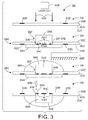
- FIG. 3 illustrated are processing steps 300 according to the present application to construct a hybrid electronics platform assembly, also shown in FIG. 3 ( i.e ., diagram 308).
- a substrate 302A is provided (in some embodiments the substrate is a flexible substrate, such as a plastic substrate).
- Substrate 302A has a first surface 302B and second surface 302C opposite the first surface. These surfaces define the height of the substrate 302A.
- the first surface 302B may include electronic circuitry 302D such as but not limited to conductive circuit tracings. Also, while shown in side view, it is understood substrate 302A of course also has width and length dimensions.
- a material removal device 302E forms an opening 302F (the opening 302F defined by the parallel downward facing arrow lines) within a pre-identified location of substrate 302A. More particularly at least one location on the first surface 302B of the substrate 302A appropriate to form the opening through the substrate is identified. Thereafter, the material removal device 302E performs a material removal operation to create the opening 302F in the substrate 302A, where the opening 302F is positioned within length and width boundaries of the substrate 302A, and the opening extends through the first surface 302B and the second surface 302C.
- the material removal device 302E is in one embodiment a laser arrangement, while in another embodiment it is a physical contact cutting device. In further embodiments other devices capable of precisely removing material to form opening 302F may be used. It is also to be understood that multiple openings may be made in a single substrate, and the assembly process of FIG. 3 may be repeated a plurality of times for that same substrate, such that multiple openings are formed.
- the opening 302F is made to conform to the shape and dimensions of a particular electronic circuit component (e.g., a bare die) being incorporated. However, a certain amount of clearance (e.g., about 5 - 25 ⁇ m) is provided to ensure the electronic circuit component 304B is capable of being received.
- the electric circuit component 304B is at least one of a bare die or pre-packaged electronic circuit component.
- diagram 304 is a modified side view, and for ease of understanding substrate material for example in front of electronic circuit component 304B is not shown. However it is to be understood that as the location of the electronic circuit component 304B is within the boundaries of the substrate 302A, there would be portions of the substrate in front of the electronic circuit component 304B, which would obstruct the view of a gap 304E, as well as the lower portion of the electronic circuit component 304B.
- FIG 304 the substrate 302A has been turned over such that first surface 302B (with circuits/traces 302D) is now facing downward.
- a flat article with a tacky upper surface e.g., a polydimethyisiloxane (PDMS) material, or other elastomer polymer which holds elements but does not permanently bond the elements together
- PDMS polydimethyisiloxane
- 304A is positioned over the opening 302F, and at least a portion of the first surface 302B of substrate 302A.
- the electronic circuit component 304B with its front surface 304C facing downward is then placed in the opening 302F.
- front surface 304C includes conductive circuit traces (including contact pads) 304G.
- the upper face of the flat article with the tacky surface 304A may be considered an alignment area 304D where the first surface 302B of substrate 302A and the first surface 304C of the electronic circuit component 304B are aligned in a substantially planar or flat or level relationship due to the flat article 304A.
- gap 304E which exists between the end of opening 302F and electronic circuit component 304B.
- the gap 304E is preferred to not be overly large, but sufficient to not interfere with the placement of the electronic circuit component 304B ( e . g ., about 5-25 ⁇ m).
- a bonding material 306A is applied on and over the second surface (backside) 306B of the electronic circuit component 304B, and on and over at least some portions of the second surface 302C of the substrate 302A.
- This backside area maybe understood to be a non-alignment area 306C where the second surface 302C of the substrate 302A and the second surface 306B of the electronic circuit component 304B are not aligned. In other words the height of the electronic circuit component 304B is greater than the height of the substrate.
- the bonding material 306A is a UV curable polymer dispensed onto the backside of the arrangement, the bonding material acting to seal the gap 304E.
- a curing arrangement (which may include curing lamps, heaters and/or other appropriate components) 306D is provided to perform curing on the UV curable polymer. After UV curing, the UV cured polymer provides a bonding structure for the assembly.
- other bonding materials known in the art may also be employed in place of the UV bonding material.
- the assembly has been turned over and the flat article (e . g ., PDMS material) 304A is separated and removed, exposing a substantially flat or planar or level surface spanning from the first surface 302B, across the filled in gap 304E' (i.e., filled in with the bonding material 306A to form a flat or planar surface), and further across the first surface 304D.
- the selected adhesive material includes the characteristics of holding the mentioned components, but when separated does not leave behind undesirable amounts of residue that would otherwise interfere with the additional assembly process.
- a cleaning of the component and substrate surfaces could be undertaken following separation and removal. By the noted operations the ramp formed by the process in FIG. 1 is eliminated.
- conductive traces 308A extending between the first surface 302B of substrate 302A and the first surface 304D electronic circuit components 304B are formed or laid down ( e . g ., the laying down being accomplished in a ramp-less structure.).
- traces 308A are generated by use of an inkjet type printing device 308B (using a conductive fluid).
- the traces may be formed by use of photolithography, which requires a flat or planar or level surface to form conductive traces.
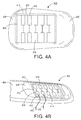
- FIGS. 4A and 4B illustrated is a top view 400 and a perspective view 402 of a silicone (Si) bare die assembly prototype.
- the size of the test die 404 is approximately 4x6mm.
- Substrate 406 is an approximately 120 ⁇ m thick polyethylene naphthalene (PEN) sheet.
- PEN polyethylene naphthalene
- a bonding material (Norland Products Inc. 83H adhesive) 408 was used.
- a cutting contour 410 is provided along the exterior area of the bare die 404. Gap 412 defines the area between the bare die 404 and the substrate cut contour 410. Also shown in this figure are contact pads 414 located on the Si bare die 404 (only certain contact pads 414 are numbered for clarity of the figure). In addition, printed connection traces 416 are shown extending off of the assembly, which causes them to pass over contact pads 414 and gap 412 (only a limited number of the printed connection traces 416 are shown and numbered for clarity of the drawing).
- bonding material 408 is on the opposite side of substrate 406 and is visible through the substrate 406, as in this prototype the substrate 406 is transparent.
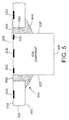
- FIG. 5 depicts an alternative embodiment of a structure formed in compliance with the general teachings of FIG. 3 .
- Side view 500 of FIG. 5 includes substrate 502A, with an upper substrate surface 502B and a lower substrate surface 502C.
- Electronic circuitry 502D such as but not limited to conductive circuit tracings is carried on upper surface 502B.
- the electronic circuitry component 503A includes an upper surface 503B, carrying electronic circuitry 503C including but not limited to contact pads.
- Component 503A further includes a backside surface 503E and sidewalls 503F and 503G.
- Conductive trace 508A extends between electronic circuit component 503A and substrate 502A, while crossing a filled gap 506A.
- Conductive trace 508A being formed by printing techniques such as inkjet type printing (using a conductive material), photolithography or other known techniques.
- bonding material 504A is applied in a less liberal manner than previous embodiments ( i.e ., see diagram 306 and bonding material 306A of FIG. 3 ).
- bonding material (which in this view has been cured) 504A is applied to fill gap 506A and extends past the gap 504A along the sidewalls 503F and 503G of the electronic circuit component 503A, as well as to a portion along the sidewalls of the substrate 502A and to a small portion of the backside surface 502C of the substrate 502A.
- this embodiment provides a more compact, less material intensive assembly.
- the process disclosed in relation to FIG. 3 may be applied in retrofitting operations.
- the substrate is a prefabricated circuit board having circuits and electronic circuit components (such as 304B, 503A).
- the process further includes retrofitting the prefabricated circuit board by at least adding an additional electronic circuit component(s) to the circuit board and/or replacing existing electronic circuit components on the prefabricated circuit board. In each case performing such retrofitting in accordance with the teachings of FIGS. 3 and 5 .
- the respective electronic circuitry is substantially level with a surface of the respective substrates.
- the present concepts are useful also when the electronic circuitry and substrates are not flush.
- the electronic circuitry or traces 600A on substrate 600, and electronic circuity or traces 602A on electronic component 602 rise in profile above the respective surfaces 600B, 602B.
- the profile is from substantially 1-20 microns, and more particularly, is in the range of 10-20 microns above the surface.
- the preceding discussion has described a method of forming a hybrid electronic assembly.
- the method is noted to include the steps of providing a substrate having a first surface and second surface opposite the first surface, the first surface including conductive circuit tracings, the substrate having height, width, and length dimensions. At least one location is identified on the first surface of the substrate to form at least one opening through the substrate. A material removal operation is performed at the identified at least one location, to create the at least one opening in the substrate at the at least one identified location. An article with an adhesive surface is attached on a first flat or planar side over the at least one opening and the at least part of the substrate on the first surface side of the substrate.
- An electronic circuit component is placed into the at least one opening at an orientation which has the first surface of the electronic circuit component pass into the opening until the first surface of the electronic circuit component engages with the elastomer material covering the opening at substantially the second surface of the substrate, wherein both the first surface of the electronic circuit component and the first surface of the substrate are placed in a substantially planar or flat or level relationship.
- a bonding material is applied to physically associate at least a portion of the electronic circuit component and at least a portion of the second surface of the substrate.
- a curing operation is performed to cure the bonding material, thereby providing a secure physical connection between the substrate and the electronic circuit component.
- the article with the tacky surface on a first flat or planar side is separated from the first surface of the electronic circuit component and the first surface of the substrate. Thereafter, conductive traces are laid down between the substrate and the electronic circuit component thereby providing electrical connections.
- the laying down is accomplished in a ramp-less structure.
- the first surface of the electronic circuit component and the first surface of the substrate includes being sufficiently level to allow the conductive traces to be formed.
- the substrate is a prefabricated circuit board, and the methods described further include retrofitting the prefabricated circuit board by at least one of adding additional electronic circuit components and replacing existing electronic circuit components on the prefabricated circuit board.
- the electronic circuit component is at least one of a bare die, and a prepackaged electronic circuit component.
- the laying down of conductive traces includes performing at least of inkjet printing, photolithography, and three-dimensional printing.
- the material removal operation is performed by one of laser cutting, melting operations, and physical contact cutting operations.
- the bonding material is in one embodiment a UV curable polymer material.
- the substrate is a plastic substrate.
- the substrate is a flexible substrate.
- the article with a tacky surface is a flat PDMS material, or elastomer material.
- the described steps form a hybrid electronic assembly which includes a substrate having a first surface and second surface opposite the first surface, which defines the height of the substrate, the first surface includes conductive circuit tracings, the substrate further including at least one opening defined within length and width dimensions of the substrate, the opening extending through the first surface and the second surface, and an electronic circuit component having a first surface and a second surface, the first surface having conductive circuit tracings, the electronic circuit component located within the at least one opening of the substrate, having height, width, and length dimensions sufficient to fit into or through the at least one opening in the substrate.
- An alignment area is provided where the first surface of the substrate and the first surface of the electronic circuit component are aligned in a substantially planar flat relationship with the electronic circuit component located within the at least one opening in the substrate.
- a non-alignment area is provided where the second surface of the substrate and the second surface of the electronic circuit component are in a non-aligned relationship, wherein the height of the electronic circuit component is greater than the height of the substrate and with the electronic circuit component located within the at least one opening the second surface of the electronic circuit component extends past the second surface of the substrate.
- a bonding material is formed on at least a portion of the second surface of the substrate and at least a portion of the electronic circuit component, the connection material encompassing sufficient portions of the substrate and the electronic circuit component to maintain the substrate and the electronic circuit component in a physically secure connection.
- Conductive traces are formed between the first surface of the substrate and the first surface of the electronic circuit component, providing electrical connections between the substrate and the electronic circuit component.
Landscapes
- Engineering & Computer Science (AREA)
- Microelectronics & Electronic Packaging (AREA)
- Manufacturing & Machinery (AREA)
- Physics & Mathematics (AREA)
- Optics & Photonics (AREA)
- Structures For Mounting Electric Components On Printed Circuit Boards (AREA)
- Electric Connection Of Electric Components To Printed Circuits (AREA)
- Non-Metallic Protective Coatings For Printed Circuits (AREA)
- Geometry (AREA)
- Manufacturing Of Printed Wiring (AREA)
Abstract
Description
- The present application is directed to electronic fabrication and more particularly fabrication of hybrid electronic platforms, which are comprised of different types of components such as integrated circuits and discrete components located on a common substrate. Hybrid electronic platforms employ cost-effective, large-area manufacturing techniques while keeping the same complex functionality and processing capability as silicon-based systems. Due to temperature and mechanical reasons, traditional silicon integration methods, such as solder bonding and wire bonding may not be suitable for hybrid platforms which may include flexible printed electronics. Various packaging techniques have been developed for chip integration on flexible substrates. For example, anisotropic conductive film (ACF) can be applied to bond and connect a chip to a circuit on a plastic substrate. However, a downside of this method is the limitation of the minimal size of the contact pads on the chip which can be bond with the adhesive.
- It is considered useful to provide techniques which overcome the noted limitations and others.
- Provided is a manufacturing process for electronic circuit components such as bare dies, and packaged integrated chips, among others, where the surface of the electronic circuit component is at the same level as the associated substrate. The surface of the electronic circuit component carries electronic elements including contact pads. A gap exists between the electronic circuit component, and the end of an opening within the substrate. This gap is filled with a filler material, such as a bonding material. The bonding material also used to encapsulate or bond together the substrate and electronic circuit component. During the manufacturing process, the front surface of the electronic circuit component, which carries electronic elements including contact pads, and the front surface of the substrate, which also carries various electronic elements, are held in an adhesive relationship by a flat material having an upper surface which includes adhesive or sticky material (such as PDMS). Once the flat material is separated and removed the planar flat or level upper surface can readily accept the formation of conductive traces by the use of inkjet printing or other technologies.
-
-
FIG. 1 illustrates a process for providing interconnects wherein a ramp is built around the components to be associated; -
FIG. 2 depicts a chip that may implement the concepts of the present application; -
FIG. 3 illustrates a process according to the present application where interconnections are made in a system where no ramp is required; -
FIGS. 4A and 4B illustrate top and perspective views of a prototype of an assembled silicone (SI) test die assembly; -
FIG. 5 depicts an alternative embodiment of a structure formed in accordance with the teachings ofFIG. 3 ; and -
FIGS 6A and 6B illustrate a substrate and an electronic circuit component which may be used in connection with the present teachings. - In the following discussion the use of the term "electronic circuit component(s)" is to be understood to include any of a number of electronic circuit configurations including but not limited to bare die, electronic packaged electronic chips, among others.
- In order to provide a manufacturing process for electronic circuit component integration on a flexible substrate, the present discussion discloses a method and structure to facilitate high resolution connection with a printing process. In the, to be disclosed structure, a surface of the electronic circuit component, which carries electronic elements including contact pads and other electronic circuitry, is at the same level as the substrate. Around the side wall of the electronic circuit component there is a filler material used to bridge the component and the substrate. The top surface of the filler is also in line or substantially level with the substrate and the electronic circuit component top surface, which holds contact pads and other electronic circuitry. This arrangement permits high resolution patterning to be readily performed to construct or lay down conductive traces or connections between the circuitry on the component and circuitry on the substrate.
- To meet the challenge of the complexity of packaging, one embodiment employs a jet based printing technology, such as one commonly referred to as inkjet printing which offers capabilities to enable high density and low resistance interconnections, and may in some embodiments be a three-dimensional (3D) type printing. With use of inkjet type technology, standard wire bonding processes can be replaced when the interconnections are made of printed conductive (such as metal) lines on a flat, planar, level area. Thus the material being printed is understood to be a printable conductive material.
- Turning to
FIG. 1 illustrated is aknown assembly process 100, represented by a series of schematic diagrams 102-108, which employs inkjet printing. Theprocess 100 includes: - As shown in a first step illustrated by diagram 102, a
non-conductive adhesive 102A is dispensed by adispensing device 102B onto an upper surface of asubstrate 102C. The non-conductive adhesive being in a semi-soft state. - Next in a second step illustrated by diagram 104,
electronic components substrate 102C such that they are in contact with thenon-conductive adhesive 102A, and may be pressed into the non-conductive material such that the non-conductive material rises up around thecomponents components curing lamp 104C. - Turning to a third step illustrated by diagram 106 an
inkjet type printer 106A is used to inkjet print circuit patterns as well asinterconnections 106B, which connect to contact areas (e.g., pads) 106C of thecomponents - Finally, in a fourth step illustrated by diagram 108 a
sintering element 108A is provided and used to sinter the printed conductive material. - A particular concept of the steps illustrated by diagrams 104 and 106 are that they utilize non-conductive adhesive to form a ramp to seal the side wall of a the
components substrate 102C. -
FIG. 2 shows anexemplary bare die 200, which has 36 contact pads 202 (not all pads numbered) with the smallest pitch about 120 um and the spacing between the pads to theedge 204 of the bare die is about 60 um. In practice, it is difficult to construct the ramp ofFIG. 1 to seal the side wall of the die without covering the contact pads of the chip or die. - In order to provide a manufacturing process for electronic circuit component integration (including bare die, packaged chips, etc.) on a flexible, substrate, the inventors have developed a method and structure to facilitate high resolution connection with appropriate printing processes. In the disclosed structure, the surface of the electronic circuit component is at substantially the same level as the substrate. Around the side wall of the electronic circuit component, there is a filler to bridge a gap between the electronic circuit component and the substrate. The top surface of the filler is also in line or substantially level or planar with the substrate surface. Therefore, high resolution patterning can be readily performed to construct conductive connections between the electronic circuit component and the circuit on the substrate, without the need of a ramp as used in the process of
FIG. 1 (i.e., the following discuses a ramp-less solution). - Turning to
FIG. 3 illustrated areprocessing steps 300 according to the present application to construct a hybrid electronics platform assembly, also shown inFIG. 3 (i.e., diagram 308). - As illustrated in diagram 302, a
substrate 302A is provided (in some embodiments the substrate is a flexible substrate, such as a plastic substrate).Substrate 302A has afirst surface 302B andsecond surface 302C opposite the first surface. These surfaces define the height of thesubstrate 302A. Thefirst surface 302B may includeelectronic circuitry 302D such as but not limited to conductive circuit tracings. Also, while shown in side view, it is understoodsubstrate 302A of course also has width and length dimensions. - A
material removal device 302E forms an opening 302F (the opening 302F defined by the parallel downward facing arrow lines) within a pre-identified location ofsubstrate 302A. More particularly at least one location on thefirst surface 302B of thesubstrate 302A appropriate to form the opening through the substrate is identified. Thereafter, thematerial removal device 302E performs a material removal operation to create the opening 302F in thesubstrate 302A, where the opening 302F is positioned within length and width boundaries of thesubstrate 302A, and the opening extends through thefirst surface 302B and thesecond surface 302C. - The
material removal device 302E is in one embodiment a laser arrangement, while in another embodiment it is a physical contact cutting device. In further embodiments other devices capable of precisely removing material to form opening 302F may be used. It is also to be understood that multiple openings may be made in a single substrate, and the assembly process ofFIG. 3 may be repeated a plurality of times for that same substrate, such that multiple openings are formed. - The opening 302F is made to conform to the shape and dimensions of a particular electronic circuit component (e.g., a bare die) being incorporated. However, a certain amount of clearance (e.g., about 5 - 25 µm) is provided to ensure the
electronic circuit component 304B is capable of being received. Theelectric circuit component 304B is at least one of a bare die or pre-packaged electronic circuit component. - In a next step shown by diagram 304, opening 302F is more clearly depicted. It is mentioned here that diagram 304 is a modified side view, and for ease of understanding substrate material for example in front of
electronic circuit component 304B is not shown. However it is to be understood that as the location of theelectronic circuit component 304B is within the boundaries of thesubstrate 302A, there would be portions of the substrate in front of theelectronic circuit component 304B, which would obstruct the view of agap 304E, as well as the lower portion of theelectronic circuit component 304B. - In diagram 304 the
substrate 302A has been turned over such thatfirst surface 302B (with circuits/traces 302D) is now facing downward. Additionally, a flat article with a tacky upper surface (e.g., a polydimethyisiloxane (PDMS) material, or other elastomer polymer which holds elements but does not permanently bond the elements together) 304A, is positioned over theopening 302F, and at least a portion of thefirst surface 302B ofsubstrate 302A. Theelectronic circuit component 304B with itsfront surface 304C facing downward is then placed in theopening 302F. It is mentionedfront surface 304C includes conductive circuit traces (including contact pads) 304G. - The upper face of the flat article with the
tacky surface 304A may be considered analignment area 304D where thefirst surface 302B ofsubstrate 302A and thefirst surface 304C of theelectronic circuit component 304B are aligned in a substantially planar or flat or level relationship due to theflat article 304A. - Also shown in diagram 304 is
gap 304E which exists between the end ofopening 302F andelectronic circuit component 304B. Thegap 304E is preferred to not be overly large, but sufficient to not interfere with the placement of theelectronic circuit component 304B (e.g., about 5-25µm). - Turning to diagram 306 of
FIG. 3 , abonding material 306A is applied on and over the second surface (backside) 306B of theelectronic circuit component 304B, and on and over at least some portions of thesecond surface 302C of thesubstrate 302A. This backside area maybe understood to be anon-alignment area 306C where thesecond surface 302C of thesubstrate 302A and thesecond surface 306B of theelectronic circuit component 304B are not aligned. In other words the height of theelectronic circuit component 304B is greater than the height of the substrate. - In one embodiment the
bonding material 306A is a UV curable polymer dispensed onto the backside of the arrangement, the bonding material acting to seal thegap 304E. A curing arrangement (which may include curing lamps, heaters and/or other appropriate components) 306D is provided to perform curing on the UV curable polymer. After UV curing, the UV cured polymer provides a bonding structure for the assembly. Of course, other bonding materials known in the art may also be employed in place of the UV bonding material. - In diagram 308 of
FIG. 3 , the assembly has been turned over and the flat article (e.g., PDMS material) 304A is separated and removed, exposing a substantially flat or planar or level surface spanning from thefirst surface 302B, across the filled ingap 304E' (i.e., filled in with thebonding material 306A to form a flat or planar surface), and further across thefirst surface 304D. It is mentioned the selected adhesive material includes the characteristics of holding the mentioned components, but when separated does not leave behind undesirable amounts of residue that would otherwise interfere with the additional assembly process. Also, as an optional step, a cleaning of the component and substrate surfaces could be undertaken following separation and removal. By the noted operations the ramp formed by the process inFIG. 1 is eliminated. - Finally,
conductive traces 308A, extending between thefirst surface 302B ofsubstrate 302A and thefirst surface 304Delectronic circuit components 304B are formed or laid down (e.g., the laying down being accomplished in a ramp-less structure.). In one embodiment traces 308A are generated by use of an inkjettype printing device 308B (using a conductive fluid). In an alternative embodiment the traces may be formed by use of photolithography, which requires a flat or planar or level surface to form conductive traces. - With continuing attention to the processing steps 302-308 of FIG.
FIG. 3 , while described are embodiments which show laser cutting (302F) being performed on a prefabricated circuit board (e.g.,substrate 302A), this order of processing can be altered. For example, laser cutting could be to a blank substrate and a bonding of thecircuit component 304B, then further a printing of a circuit with the connection path. - Turning to
FIGS. 4A and 4B , illustrated is atop view 400 and aperspective view 402 of a silicone (Si) bare die assembly prototype. In accordance with teachings of the present application, the size of the test die 404 is approximately 4x6mm.Substrate 406 is an approximately 120µm thick polyethylene naphthalene (PEN) sheet. For the prototype, a bonding material (Norland Products Inc. 83H adhesive) 408 was used. - A cutting
contour 410 is provided along the exterior area of thebare die 404.Gap 412 defines the area between thebare die 404 and thesubstrate cut contour 410. Also shown in this figure arecontact pads 414 located on the Si bare die 404 (onlycertain contact pads 414 are numbered for clarity of the figure). In addition, printed connection traces 416 are shown extending off of the assembly, which causes them to pass overcontact pads 414 and gap 412 (only a limited number of the printed connection traces 416 are shown and numbered for clarity of the drawing). - It is to be appreciated that
bonding material 408 is on the opposite side ofsubstrate 406 and is visible through thesubstrate 406, as in this prototype thesubstrate 406 is transparent. -
FIG. 5 depicts an alternative embodiment of a structure formed in compliance with the general teachings ofFIG. 3 . - Side view 500 of
FIG. 5 includessubstrate 502A, with anupper substrate surface 502B and alower substrate surface 502C.Electronic circuitry 502D, such as but not limited to conductive circuit tracings is carried onupper surface 502B. In this embodiment, theelectronic circuitry component 503A includes anupper surface 503B, carryingelectronic circuitry 503C including but not limited to contact pads.Component 503A further includes abackside surface 503E and sidewalls 503F and 503G. Conductive trace 508A extends betweenelectronic circuit component 503A andsubstrate 502A, while crossing a filledgap 506A. Conductive trace 508A being formed by printing techniques such as inkjet type printing (using a conductive material), photolithography or other known techniques. - In this embodiment of
FIG. 5 , a particular distinction is thatbonding material 504A is applied in a less liberal manner than previous embodiments (i.e., see diagram 306 andbonding material 306A ofFIG. 3 ). Particularly, bonding material (which in this view has been cured) 504A is applied to fillgap 506A and extends past thegap 504A along thesidewalls electronic circuit component 503A, as well as to a portion along the sidewalls of thesubstrate 502A and to a small portion of thebackside surface 502C of thesubstrate 502A. Thus, this embodiment provides a more compact, less material intensive assembly. - In another embodiment the process disclosed in relation to
FIG. 3 (andFIG. 5 ) may be applied in retrofitting operations. For example, in these situations the substrate is a prefabricated circuit board having circuits and electronic circuit components (such as 304B, 503A). In this situation the process further includes retrofitting the prefabricated circuit board by at least adding an additional electronic circuit component(s) to the circuit board and/or replacing existing electronic circuit components on the prefabricated circuit board. In each case performing such retrofitting in accordance with the teachings ofFIGS. 3 and5 . - Turning now to
FIGS. 6A and 6B , in the foregoing embodiments, the respective electronic circuitry is substantially level with a surface of the respective substrates. However, it is to be understood the present concepts are useful also when the electronic circuitry and substrates are not flush. For example, inFIGS. 6A and 6B , illustrated is asubstrate 600 and an electronic circuit component 602. As can be seen, the electronic circuitry or traces 600A onsubstrate 600, and electronic circuity or traces 602A on electronic component 602, rise in profile above therespective surfaces FIGS. 6A and 6B , as well as those shown in the foregoing figures, and the same types of processes will be used. It is to be mentioned that, for example, when the electronic circuitry component is placed in contact with a material (for example, PDMS) which is sufficiently soft, this allows the electronic circuitry component to push into the PDMS material providing it with appropriate positioning for the remainder of the process to be undertaken. - Similarly, when a conductive trace on a substrate is applied to elements such as those of 600 and 602, there is sufficient depositing height to generate a substantially flat circuitry line such as shown in the preceding figures.
- The preceding discussion has described a method of forming a hybrid electronic assembly. The method is noted to include the steps of providing a substrate having a first surface and second surface opposite the first surface, the first surface including conductive circuit tracings, the substrate having height, width, and length dimensions. At least one location is identified on the first surface of the substrate to form at least one opening through the substrate. A material removal operation is performed at the identified at least one location, to create the at least one opening in the substrate at the at least one identified location. An article with an adhesive surface is attached on a first flat or planar side over the at least one opening and the at least part of the substrate on the first surface side of the substrate. An electronic circuit component is placed into the at least one opening at an orientation which has the first surface of the electronic circuit component pass into the opening until the first surface of the electronic circuit component engages with the elastomer material covering the opening at substantially the second surface of the substrate, wherein both the first surface of the electronic circuit component and the first surface of the substrate are placed in a substantially planar or flat or level relationship. A bonding material is applied to physically associate at least a portion of the electronic circuit component and at least a portion of the second surface of the substrate. A curing operation is performed to cure the bonding material, thereby providing a secure physical connection between the substrate and the electronic circuit component. The article with the tacky surface on a first flat or planar side is separated from the first surface of the electronic circuit component and the first surface of the substrate. Thereafter, conductive traces are laid down between the substrate and the electronic circuit component thereby providing electrical connections.
- Aspects of the above described method are set forth below.
- The laying down is accomplished in a ramp-less structure.
- The first surface of the electronic circuit component and the first surface of the substrate includes being sufficiently level to allow the conductive traces to be formed.
- The substrate is a prefabricated circuit board, and the methods described further include retrofitting the prefabricated circuit board by at least one of adding additional electronic circuit components and replacing existing electronic circuit components on the prefabricated circuit board.
- The electronic circuit component is at least one of a bare die, and a prepackaged electronic circuit component.
- The laying down of conductive traces includes performing at least of inkjet printing, photolithography, and three-dimensional printing.
- The material removal operation is performed by one of laser cutting, melting operations, and physical contact cutting operations.
- The bonding material is in one embodiment a UV curable polymer material.
- The substrate is a plastic substrate.
- The substrate is a flexible substrate.
- The article with a tacky surface is a flat PDMS material, or elastomer material.
- The described steps form a hybrid electronic assembly which includes a substrate having a first surface and second surface opposite the first surface, which defines the height of the substrate, the first surface includes conductive circuit tracings, the substrate further including at least one opening defined within length and width dimensions of the substrate, the opening extending through the first surface and the second surface, and an electronic circuit component having a first surface and a second surface, the first surface having conductive circuit tracings, the electronic circuit component located within the at least one opening of the substrate, having height, width, and length dimensions sufficient to fit into or through the at least one opening in the substrate. An alignment area is provided where the first surface of the substrate and the first surface of the electronic circuit component are aligned in a substantially planar flat relationship with the electronic circuit component located within the at least one opening in the substrate. A non-alignment area is provided where the second surface of the substrate and the second surface of the electronic circuit component are in a non-aligned relationship, wherein the height of the electronic circuit component is greater than the height of the substrate and with the electronic circuit component located within the at least one opening the second surface of the electronic circuit component extends past the second surface of the substrate. A bonding material is formed on at least a portion of the second surface of the substrate and at least a portion of the electronic circuit component, the connection material encompassing sufficient portions of the substrate and the electronic circuit component to maintain the substrate and the electronic circuit component in a physically secure connection. Conductive traces are formed between the first surface of the substrate and the first surface of the electronic circuit component, providing electrical connections between the substrate and the electronic circuit component.
- It will be appreciated that variants of the above-disclosed and other features and functions, or alternatives thereof, may be combined into many other different systems or applications. Various presently unforeseen or unanticipated alternatives, modifications, variations or improvements therein may be subsequently made by those skilled in the art which are also intended to be encompassed by the following claims.
Claims (10)
- A method of forming a hybrid electronic assembly comprising:providing a substrate having a first surface and second surface opposite the first surface, the first surface including conductive circuit tracings, the substrate having height, width, and length dimensions;identifying at least one location on the first surface of the substrate to form at least one opening through the substrate;performing a material removal operation at the identified at least one location, to create the at least one opening in the substrate at the at least one identified location;attaching an article with a sticking surface on a first flat or planar side over the at least one opening and the at least part of the substrate on the first surface side of the substrate;placing an electronic circuit component into the at least one opening at an orientation which has the first surface of the electronic circuit component pass into the opening until the first surface of the electronic circuit component engages with the elastomer material covering the opening at substantially the second surface of the substrate, wherein both the first surface of the electronic circuit component and the first surface of the substrate are placed in a substantially planar or flat or level relationship;applying a bonding material to physically associate at least a portion of the electronic circuit component and at least a portion of the second surface of the substrate;performing a curing operation to cure the bonding material, thereby providing a secure physical connection between the substrate and the electronic circuit component;separating the article with the tacky surface on a first flat or planar side from the first surface of the electronic circuit component and the first surface of the substrate; andlaying down conductive traces between the substrate and the electronic circuit component thereby providing electrical connections.
- The method according to claim 1 wherein the laying down is accomplished in a ramp-less structure.
- The method according to claim 1 wherein the first surface of the electronic circuit component and the first surface of the substrate includes being sufficiently level to allow the conductive traces to be formed.
- The method according to claim 1 wherein the substrate is a prefabricated circuit board, and the method further includes retrofitting the prefabricated circuit board by at least one of adding additional electronic circuit components and replacing existing electronic circuit components on the prefabricated circuit board.
- The method according to claim 1 wherein the electronic circuit component is at least one of a bare die, and a prepackaged electronic circuit component.
- The method according to claim 1 wherein the laying down of conductive traces includes performing at least on of inkjet printing, photolithography, and three-dimensional printing.
- A hybrid electronic assembly comprising:a substrate having a first surface and second surface opposite the first surface, which defines the height of the substrate, the first surface including conductive circuit tracings, the substrate further including at least one opening defined within length and width dimensions of the substrate, the opening extending through the first surface and the second surface;an electronic circuit component having a first surface and a second surface, the first surface having conductive circuit tracings, the electronic circuit component located within the at least one opening of the substrate, having height, width, and length dimensions sufficient to fit into or through the at least one opening in the substrate;an alignment area where the first surface of the substrate and the first surface of the electronic circuit component are aligned in a substantially planar flat relationship with the electronic circuit component located within the at least one opening in the substrate;a non-alignment area where the second surface of the substrate and the second surface of the electronic circuit component are in a non-aligned relationship, wherein the height of the electronic circuit component is greater than the height of the substrate and with the electronic circuit component located within the at least one opening the second surface of the electronic circuit component extends past the second surface of the substrate;a bonding material formed at least a portion of the second surface of the substrate and at least a portion of the electronic circuit component, the bonding material encompassing sufficient portions of the substrate and the electronic circuit component to maintain the substrate and the electronic circuit component in a physically secure connection; andconductive traces formed between the first surface of the substrate and the first surface of the electronic circuit component, providing electrical connections between the substrate and the electronic circuit component.
- The assembly according to claim 1 wherein the laying down is accomplished in a ramp-less structure.
- The assembly according to claim 1 wherein substantially planar or flat or level with the first surface of the electronic circuit component and the first surface of the substrate includes being sufficiently level to allow the conductive traces to be formed.
- The assembly according to claim 1 wherein the substrate is a prefabricated circuit board, and the assembly is a retrofit assembly which includes additional electronic circuit components to the prefabricated circuit board.
Applications Claiming Priority (2)
| Application Number | Priority Date | Filing Date | Title |
|---|---|---|---|
| US201562204706P | 2015-08-13 | 2015-08-13 | |
| US14/964,964 US10206288B2 (en) | 2015-08-13 | 2015-12-10 | Bare die integration with printed components on flexible substrate |
Publications (2)
| Publication Number | Publication Date |
|---|---|
| EP3131114A1 true EP3131114A1 (en) | 2017-02-15 |
| EP3131114B1 EP3131114B1 (en) | 2021-04-07 |
Family
ID=56787268
Family Applications (1)
| Application Number | Title | Priority Date | Filing Date |
|---|---|---|---|
| EP16183143.3A Active EP3131114B1 (en) | 2015-08-13 | 2016-08-05 | Bare die integration within a flexible substrate |
Country Status (3)
| Country | Link |
|---|---|
| US (1) | US10206288B2 (en) |
| EP (1) | EP3131114B1 (en) |
| JP (1) | JP6803168B2 (en) |
Families Citing this family (7)
| Publication number | Priority date | Publication date | Assignee | Title |
|---|---|---|---|---|
| US10206288B2 (en) * | 2015-08-13 | 2019-02-12 | Palo Alto Research Center Incorporated | Bare die integration with printed components on flexible substrate |
| US10165677B2 (en) | 2015-12-10 | 2018-12-25 | Palo Alto Research Center Incorporated | Bare die integration with printed components on flexible substrate without laser cut |
| EP3602642A4 (en) | 2017-03-31 | 2020-12-23 | 3M Innovative Properties Company | ELECTRONIC DEVICES WITH FIXED SEMI-CONDUCTOR CHIPS |
| US10847384B2 (en) | 2017-05-31 | 2020-11-24 | Palo Alto Research Center Incorporated | Method and fixture for chip attachment to physical objects |
| US10795452B2 (en) | 2018-02-07 | 2020-10-06 | Microsoft Technology Licensing, Llc | Multi-stage cure bare die light emitting diode |
| CN113130330B (en) * | 2021-03-17 | 2024-05-24 | 浙江臻镭科技股份有限公司 | Novel chip surface mounting structure and preparation method thereof |
| CN114068476B (en) * | 2021-10-13 | 2025-12-23 | 日月光半导体制造股份有限公司 | Semiconductor packaging structure and its formation method |
Citations (4)
| Publication number | Priority date | Publication date | Assignee | Title |
|---|---|---|---|---|
| US4850105A (en) * | 1987-07-04 | 1989-07-25 | Horiba, Ltd. | Method of taking out lead of semiconductor tip part |
| WO2011127328A2 (en) * | 2010-04-07 | 2011-10-13 | Intellipaper, Llc | Electronic assemblies and methods of forming electronic assemblies |
| US20140177177A1 (en) * | 2012-12-25 | 2014-06-26 | National Taipei University Of Technology | Electronic device and fabrication method thereof |
| US20140239497A1 (en) * | 2013-02-28 | 2014-08-28 | Weng F. Yap | Packaged semiconductor device |
Family Cites Families (27)
| Publication number | Priority date | Publication date | Assignee | Title |
|---|---|---|---|---|
| FR2527036A1 (en) * | 1982-05-14 | 1983-11-18 | Radiotechnique Compelec | METHOD FOR CONNECTING A SEMICONDUCTOR TO ELEMENTS OF A SUPPORT, PARTICULARLY A PORTABLE CARD |
| US4658330A (en) * | 1985-09-09 | 1987-04-14 | Tektronix, Inc. | Mounting a hybrid circuit to a circuit board |
| US5976912A (en) | 1994-03-18 | 1999-11-02 | Hitachi Chemical Company, Ltd. | Fabrication process of semiconductor package and semiconductor package |
| JPH11238956A (en) * | 1998-02-23 | 1999-08-31 | Omron Corp | Mounting structure of electronic components and IC sheet that can read electromagnetic waves |
| US6815251B1 (en) * | 1999-02-01 | 2004-11-09 | Micron Technology, Inc. | High density modularity for IC's |
| JP4649745B2 (en) | 2001-02-01 | 2011-03-16 | ソニー株式会社 | Light-emitting element transfer method |
| JP4386008B2 (en) * | 2004-11-11 | 2009-12-16 | セイコーエプソン株式会社 | Mounting board and electronic equipment |
| US7208345B2 (en) | 2005-05-11 | 2007-04-24 | Infineon Technologies Ag | Method of manufacturing a semiconductor device comprising stacked chips and a corresponding semiconductor device |
| JP4538416B2 (en) | 2006-02-03 | 2010-09-08 | 株式会社日立メディアエレクトロニクス | Optical pickup device, manufacturing method thereof, and optical drive device |
| US9681550B2 (en) * | 2007-08-28 | 2017-06-13 | Joseph C. Fjelstad | Method of making a circuit subassembly |
| KR20100009896A (en) | 2008-07-21 | 2010-01-29 | 삼성전자주식회사 | Semiconductor device package and method of fabricating the same |
| JP2010251376A (en) * | 2009-04-10 | 2010-11-04 | Sumitomo Electric Printed Circuit Inc | Wiring body, method of manufacturing the same, and electronic equipment |
| WO2011128266A1 (en) | 2010-04-12 | 2011-10-20 | Imec | Optical shear sensor and method of producing such an optical shear sensor |
| JP5512888B2 (en) * | 2010-06-29 | 2014-06-04 | クーレッジ ライティング インコーポレイテッド | Electronic device with flexible substrate |
| KR20120004777A (en) | 2010-07-07 | 2012-01-13 | 삼성전기주식회사 | Electronic component module and manufacturing method thereof |
| US8501544B2 (en) | 2010-08-31 | 2013-08-06 | Stats Chippac, Ltd. | Semiconductor device and method of forming adhesive material over semiconductor die and carrier to reduce die shifting during encapsulation |
| US20140291001A1 (en) * | 2010-11-22 | 2014-10-02 | Bridge Semiconductor Corporation | Method of making hybrid wiring board with built-in stiffener and interposer and hybrid wiring board manufactured thereby |
| US20120268899A1 (en) | 2011-04-21 | 2012-10-25 | Tessera Research Llc | Reinforced fan-out wafer-level package |
| US8937382B2 (en) * | 2011-06-27 | 2015-01-20 | Intel Corporation | Secondary device integration into coreless microelectronic device packages |
| US10388584B2 (en) | 2011-09-06 | 2019-08-20 | STATS ChipPAC Pte. Ltd. | Semiconductor device and method of forming Fo-WLCSP with recessed interconnect area in peripheral region of semiconductor die |
| EP2639278A1 (en) | 2012-03-13 | 2013-09-18 | Nitto Denko Corporation | Heat-resistant pressure-sensitive adhesive tape for production of semiconductor device and method for producing seminconductor device using the tape |
| DE102013201926B4 (en) | 2013-02-06 | 2025-12-04 | Robert Bosch Gmbh | Methods for electrically contacting a component and component assembly |
| TWI518852B (en) | 2013-10-02 | 2016-01-21 | 矽品精密工業股份有限公司 | Semiconductor package and its manufacturing method |
| CN104701190A (en) | 2013-12-06 | 2015-06-10 | 毅宝力科技有限公司 | Systems and methods for fabricating cavity-down fabrication carriers |
| US9396972B2 (en) | 2014-02-11 | 2016-07-19 | Palo Alto Research Center Incorporated | Micro-assembly with planarized embedded microelectronic dies |
| US10206288B2 (en) * | 2015-08-13 | 2019-02-12 | Palo Alto Research Center Incorporated | Bare die integration with printed components on flexible substrate |
| US10165677B2 (en) * | 2015-12-10 | 2018-12-25 | Palo Alto Research Center Incorporated | Bare die integration with printed components on flexible substrate without laser cut |
-
2015
- 2015-12-10 US US14/964,964 patent/US10206288B2/en active Active
-
2016
- 2016-07-28 JP JP2016149036A patent/JP6803168B2/en active Active
- 2016-08-05 EP EP16183143.3A patent/EP3131114B1/en active Active
Patent Citations (4)
| Publication number | Priority date | Publication date | Assignee | Title |
|---|---|---|---|---|
| US4850105A (en) * | 1987-07-04 | 1989-07-25 | Horiba, Ltd. | Method of taking out lead of semiconductor tip part |
| WO2011127328A2 (en) * | 2010-04-07 | 2011-10-13 | Intellipaper, Llc | Electronic assemblies and methods of forming electronic assemblies |
| US20140177177A1 (en) * | 2012-12-25 | 2014-06-26 | National Taipei University Of Technology | Electronic device and fabrication method thereof |
| US20140239497A1 (en) * | 2013-02-28 | 2014-08-28 | Weng F. Yap | Packaged semiconductor device |
Also Published As
| Publication number | Publication date |
|---|---|
| US20170048986A1 (en) | 2017-02-16 |
| EP3131114B1 (en) | 2021-04-07 |
| US10206288B2 (en) | 2019-02-12 |
| JP2017038046A (en) | 2017-02-16 |
| JP6803168B2 (en) | 2020-12-23 |
Similar Documents
| Publication | Publication Date | Title |
|---|---|---|
| EP3131114B1 (en) | Bare die integration within a flexible substrate | |
| US11122683B2 (en) | Bare die integration with printed components on flexible substrate without laser cut | |
| CN105165129B (en) | Manufacturing method of resin multilayer substrate | |
| US6426564B1 (en) | Recessed tape and method for forming a BGA assembly | |
| EP3940773A1 (en) | Method of surface-mounting components | |
| KR101768789B1 (en) | Printing complex electronic circuits | |
| JP2022542011A (en) | Method for producing anisotropic conductive adhesive film in which separation distance of conductive particles is controlled | |
| CN110603633B (en) | Carrier and assembly of a plurality of electrical circuits fixed to the carrier and method of manufacturing the same | |
| US11937381B2 (en) | Forming electrical interconnections using capillary microfluidics | |
| US10477699B2 (en) | Method for manufacturing electronic component attached wiring board | |
| US8042267B2 (en) | Method for producing microsystems | |
| CN106696475A (en) | 3D (Three-dimensional) printer and method for utilizing 3D printer for printing printed circuit board | |
| US20180350729A1 (en) | Method and fixture for chip attachment to physical objects | |
| CN206907790U (en) | Printed conductive structure and light emitting module including the same | |
| CN111263535A (en) | Method for manufacturing printed circuit board | |
| WO2019098029A1 (en) | Electronic device and manufacturing method thereof | |
| CN107548573A (en) | Printed circuit board to mold compound junction | |
| CN117915562A (en) | Circuit board and manufacturing method thereof | |
| CN111316426B (en) | Electronic device and manufacturing method thereof | |
| TW201128949A (en) | Laminated flexible circuit board, a manufacturing method | |
| CN104241145A (en) | Method for Producing a Semiconductor Module by Using an Adhesion Carrier | |
| US20100132990A1 (en) | Device Built By Joining A Plurality Of Layers | |
| JP2007180397A (en) | Printed wiring board and liquid crystal display device | |
| TW201922072A (en) | Method to neutralize incorrectly oriented printed diodes | |
| CN121768287A (en) | Display panel and manufacturing method thereof |
Legal Events
| Date | Code | Title | Description |
|---|---|---|---|
| PUAI | Public reference made under article 153(3) epc to a published international application that has entered the european phase |
Free format text: ORIGINAL CODE: 0009012 |
|
| STAA | Information on the status of an ep patent application or granted ep patent |
Free format text: STATUS: THE APPLICATION HAS BEEN PUBLISHED |
|
| AK | Designated contracting states |
Kind code of ref document: A1 Designated state(s): AL AT BE BG CH CY CZ DE DK EE ES FI FR GB GR HR HU IE IS IT LI LT LU LV MC MK MT NL NO PL PT RO RS SE SI SK SM TR |
|
| AX | Request for extension of the european patent |
Extension state: BA ME |
|
| STAA | Information on the status of an ep patent application or granted ep patent |
Free format text: STATUS: REQUEST FOR EXAMINATION WAS MADE |
|
| 17P | Request for examination filed |
Effective date: 20170816 |
|
| RBV | Designated contracting states (corrected) |
Designated state(s): AL AT BE BG CH CY CZ DE DK EE ES FI FR GB GR HR HU IE IS IT LI LT LU LV MC MK MT NL NO PL PT RO RS SE SI SK SM TR |
|
| STAA | Information on the status of an ep patent application or granted ep patent |
Free format text: STATUS: EXAMINATION IS IN PROGRESS |
|
| 17Q | First examination report despatched |
Effective date: 20200610 |
|
| RIC1 | Information provided on ipc code assigned before grant |
Ipc: H01L 23/498 20060101ALI20200924BHEP Ipc: H05K 3/28 20060101ALI20200924BHEP Ipc: H01L 21/683 20060101ALI20200924BHEP Ipc: H01L 21/56 20060101ALI20200924BHEP Ipc: H05K 1/18 20060101ALI20200924BHEP Ipc: H05K 3/22 20060101ALI20200924BHEP Ipc: H01L 21/67 20060101ALI20200924BHEP Ipc: H01L 23/485 20060101ALI20200924BHEP Ipc: H05K 3/30 20060101ALI20200924BHEP Ipc: H01L 21/60 20060101AFI20200924BHEP Ipc: H01L 23/13 20060101ALI20200924BHEP |
|
| GRAP | Despatch of communication of intention to grant a patent |
Free format text: ORIGINAL CODE: EPIDOSNIGR1 |
|
| STAA | Information on the status of an ep patent application or granted ep patent |
Free format text: STATUS: GRANT OF PATENT IS INTENDED |
|
| INTG | Intention to grant announced |
Effective date: 20201105 |
|
| GRAS | Grant fee paid |
Free format text: ORIGINAL CODE: EPIDOSNIGR3 |
|
| GRAA | (expected) grant |
Free format text: ORIGINAL CODE: 0009210 |
|
| STAA | Information on the status of an ep patent application or granted ep patent |
Free format text: STATUS: THE PATENT HAS BEEN GRANTED |
|
| AK | Designated contracting states |
Kind code of ref document: B1 Designated state(s): AL AT BE BG CH CY CZ DE DK EE ES FI FR GB GR HR HU IE IS IT LI LT LU LV MC MK MT NL NO PL PT RO RS SE SI SK SM TR |
|
| REG | Reference to a national code |
Ref country code: GB Ref legal event code: FG4D |
|
| REG | Reference to a national code |
Ref country code: AT Ref legal event code: REF Ref document number: 1380785 Country of ref document: AT Kind code of ref document: T Effective date: 20210415 Ref country code: CH Ref legal event code: EP |
|
| REG | Reference to a national code |
Ref country code: DE Ref legal event code: R096 Ref document number: 602016055540 Country of ref document: DE |
|
| REG | Reference to a national code |
Ref country code: IE Ref legal event code: FG4D |
|
| REG | Reference to a national code |
Ref country code: LT Ref legal event code: MG9D |
|
| REG | Reference to a national code |
Ref country code: NL Ref legal event code: MP Effective date: 20210407 Ref country code: AT Ref legal event code: MK05 Ref document number: 1380785 Country of ref document: AT Kind code of ref document: T Effective date: 20210407 |
|
| PG25 | Lapsed in a contracting state [announced via postgrant information from national office to epo] |
Ref country code: NL Free format text: LAPSE BECAUSE OF FAILURE TO SUBMIT A TRANSLATION OF THE DESCRIPTION OR TO PAY THE FEE WITHIN THE PRESCRIBED TIME-LIMIT Effective date: 20210407 Ref country code: LT Free format text: LAPSE BECAUSE OF FAILURE TO SUBMIT A TRANSLATION OF THE DESCRIPTION OR TO PAY THE FEE WITHIN THE PRESCRIBED TIME-LIMIT Effective date: 20210407 Ref country code: FI Free format text: LAPSE BECAUSE OF FAILURE TO SUBMIT A TRANSLATION OF THE DESCRIPTION OR TO PAY THE FEE WITHIN THE PRESCRIBED TIME-LIMIT Effective date: 20210407 Ref country code: AT Free format text: LAPSE BECAUSE OF FAILURE TO SUBMIT A TRANSLATION OF THE DESCRIPTION OR TO PAY THE FEE WITHIN THE PRESCRIBED TIME-LIMIT Effective date: 20210407 Ref country code: BG Free format text: LAPSE BECAUSE OF FAILURE TO SUBMIT A TRANSLATION OF THE DESCRIPTION OR TO PAY THE FEE WITHIN THE PRESCRIBED TIME-LIMIT Effective date: 20210707 Ref country code: HR Free format text: LAPSE BECAUSE OF FAILURE TO SUBMIT A TRANSLATION OF THE DESCRIPTION OR TO PAY THE FEE WITHIN THE PRESCRIBED TIME-LIMIT Effective date: 20210407 |
|
| PG25 | Lapsed in a contracting state [announced via postgrant information from national office to epo] |
Ref country code: GR Free format text: LAPSE BECAUSE OF FAILURE TO SUBMIT A TRANSLATION OF THE DESCRIPTION OR TO PAY THE FEE WITHIN THE PRESCRIBED TIME-LIMIT Effective date: 20210708 Ref country code: IS Free format text: LAPSE BECAUSE OF FAILURE TO SUBMIT A TRANSLATION OF THE DESCRIPTION OR TO PAY THE FEE WITHIN THE PRESCRIBED TIME-LIMIT Effective date: 20210807 Ref country code: LV Free format text: LAPSE BECAUSE OF FAILURE TO SUBMIT A TRANSLATION OF THE DESCRIPTION OR TO PAY THE FEE WITHIN THE PRESCRIBED TIME-LIMIT Effective date: 20210407 Ref country code: ES Free format text: LAPSE BECAUSE OF FAILURE TO SUBMIT A TRANSLATION OF THE DESCRIPTION OR TO PAY THE FEE WITHIN THE PRESCRIBED TIME-LIMIT Effective date: 20210407 Ref country code: PT Free format text: LAPSE BECAUSE OF FAILURE TO SUBMIT A TRANSLATION OF THE DESCRIPTION OR TO PAY THE FEE WITHIN THE PRESCRIBED TIME-LIMIT Effective date: 20210809 Ref country code: NO Free format text: LAPSE BECAUSE OF FAILURE TO SUBMIT A TRANSLATION OF THE DESCRIPTION OR TO PAY THE FEE WITHIN THE PRESCRIBED TIME-LIMIT Effective date: 20210707 Ref country code: PL Free format text: LAPSE BECAUSE OF FAILURE TO SUBMIT A TRANSLATION OF THE DESCRIPTION OR TO PAY THE FEE WITHIN THE PRESCRIBED TIME-LIMIT Effective date: 20210407 Ref country code: RS Free format text: LAPSE BECAUSE OF FAILURE TO SUBMIT A TRANSLATION OF THE DESCRIPTION OR TO PAY THE FEE WITHIN THE PRESCRIBED TIME-LIMIT Effective date: 20210407 Ref country code: SE Free format text: LAPSE BECAUSE OF FAILURE TO SUBMIT A TRANSLATION OF THE DESCRIPTION OR TO PAY THE FEE WITHIN THE PRESCRIBED TIME-LIMIT Effective date: 20210407 |
|
| REG | Reference to a national code |
Ref country code: DE Ref legal event code: R097 Ref document number: 602016055540 Country of ref document: DE |
|
| PG25 | Lapsed in a contracting state [announced via postgrant information from national office to epo] |
Ref country code: DK Free format text: LAPSE BECAUSE OF FAILURE TO SUBMIT A TRANSLATION OF THE DESCRIPTION OR TO PAY THE FEE WITHIN THE PRESCRIBED TIME-LIMIT Effective date: 20210407 Ref country code: EE Free format text: LAPSE BECAUSE OF FAILURE TO SUBMIT A TRANSLATION OF THE DESCRIPTION OR TO PAY THE FEE WITHIN THE PRESCRIBED TIME-LIMIT Effective date: 20210407 Ref country code: CZ Free format text: LAPSE BECAUSE OF FAILURE TO SUBMIT A TRANSLATION OF THE DESCRIPTION OR TO PAY THE FEE WITHIN THE PRESCRIBED TIME-LIMIT Effective date: 20210407 Ref country code: SM Free format text: LAPSE BECAUSE OF FAILURE TO SUBMIT A TRANSLATION OF THE DESCRIPTION OR TO PAY THE FEE WITHIN THE PRESCRIBED TIME-LIMIT Effective date: 20210407 Ref country code: SK Free format text: LAPSE BECAUSE OF FAILURE TO SUBMIT A TRANSLATION OF THE DESCRIPTION OR TO PAY THE FEE WITHIN THE PRESCRIBED TIME-LIMIT Effective date: 20210407 Ref country code: RO Free format text: LAPSE BECAUSE OF FAILURE TO SUBMIT A TRANSLATION OF THE DESCRIPTION OR TO PAY THE FEE WITHIN THE PRESCRIBED TIME-LIMIT Effective date: 20210407 |
|
| PLBE | No opposition filed within time limit |
Free format text: ORIGINAL CODE: 0009261 |
|
| STAA | Information on the status of an ep patent application or granted ep patent |
Free format text: STATUS: NO OPPOSITION FILED WITHIN TIME LIMIT |
|
| 26N | No opposition filed |
Effective date: 20220110 |
|
| REG | Reference to a national code |
Ref country code: CH Ref legal event code: PL |
|
| PG25 | Lapsed in a contracting state [announced via postgrant information from national office to epo] |
Ref country code: MC Free format text: LAPSE BECAUSE OF FAILURE TO SUBMIT A TRANSLATION OF THE DESCRIPTION OR TO PAY THE FEE WITHIN THE PRESCRIBED TIME-LIMIT Effective date: 20210407 |
|
| REG | Reference to a national code |
Ref country code: BE Ref legal event code: MM Effective date: 20210831 |
|
| PG25 | Lapsed in a contracting state [announced via postgrant information from national office to epo] |
Ref country code: LI Free format text: LAPSE BECAUSE OF NON-PAYMENT OF DUE FEES Effective date: 20210831 Ref country code: CH Free format text: LAPSE BECAUSE OF NON-PAYMENT OF DUE FEES Effective date: 20210831 |
|
| PG25 | Lapsed in a contracting state [announced via postgrant information from national office to epo] |
Ref country code: IS Free format text: LAPSE BECAUSE OF FAILURE TO SUBMIT A TRANSLATION OF THE DESCRIPTION OR TO PAY THE FEE WITHIN THE PRESCRIBED TIME-LIMIT Effective date: 20210807 Ref country code: LU Free format text: LAPSE BECAUSE OF NON-PAYMENT OF DUE FEES Effective date: 20210805 Ref country code: AL Free format text: LAPSE BECAUSE OF FAILURE TO SUBMIT A TRANSLATION OF THE DESCRIPTION OR TO PAY THE FEE WITHIN THE PRESCRIBED TIME-LIMIT Effective date: 20210407 |
|
| PG25 | Lapsed in a contracting state [announced via postgrant information from national office to epo] |
Ref country code: IT Free format text: LAPSE BECAUSE OF FAILURE TO SUBMIT A TRANSLATION OF THE DESCRIPTION OR TO PAY THE FEE WITHIN THE PRESCRIBED TIME-LIMIT Effective date: 20210407 Ref country code: IE Free format text: LAPSE BECAUSE OF NON-PAYMENT OF DUE FEES Effective date: 20210805 Ref country code: BE Free format text: LAPSE BECAUSE OF NON-PAYMENT OF DUE FEES Effective date: 20210831 |
|
| PG25 | Lapsed in a contracting state [announced via postgrant information from national office to epo] |
Ref country code: HU Free format text: LAPSE BECAUSE OF FAILURE TO SUBMIT A TRANSLATION OF THE DESCRIPTION OR TO PAY THE FEE WITHIN THE PRESCRIBED TIME-LIMIT; INVALID AB INITIO Effective date: 20160805 |
|
| PG25 | Lapsed in a contracting state [announced via postgrant information from national office to epo] |
Ref country code: CY Free format text: LAPSE BECAUSE OF FAILURE TO SUBMIT A TRANSLATION OF THE DESCRIPTION OR TO PAY THE FEE WITHIN THE PRESCRIBED TIME-LIMIT Effective date: 20210407 |
|
| PG25 | Lapsed in a contracting state [announced via postgrant information from national office to epo] |
Ref country code: MK Free format text: LAPSE BECAUSE OF FAILURE TO SUBMIT A TRANSLATION OF THE DESCRIPTION OR TO PAY THE FEE WITHIN THE PRESCRIBED TIME-LIMIT Effective date: 20210407 |
|
| PG25 | Lapsed in a contracting state [announced via postgrant information from national office to epo] |
Ref country code: TR Free format text: LAPSE BECAUSE OF FAILURE TO SUBMIT A TRANSLATION OF THE DESCRIPTION OR TO PAY THE FEE WITHIN THE PRESCRIBED TIME-LIMIT Effective date: 20210407 |
|
| PG25 | Lapsed in a contracting state [announced via postgrant information from national office to epo] |
Ref country code: MT Free format text: LAPSE BECAUSE OF FAILURE TO SUBMIT A TRANSLATION OF THE DESCRIPTION OR TO PAY THE FEE WITHIN THE PRESCRIBED TIME-LIMIT Effective date: 20210407 |
|
| PGFP | Annual fee paid to national office [announced via postgrant information from national office to epo] |
Ref country code: DE Payment date: 20250724 Year of fee payment: 10 |
|
| PGFP | Annual fee paid to national office [announced via postgrant information from national office to epo] |
Ref country code: GB Payment date: 20250725 Year of fee payment: 10 |
|
| PGFP | Annual fee paid to national office [announced via postgrant information from national office to epo] |
Ref country code: FR Payment date: 20250723 Year of fee payment: 10 |
|
| REG | Reference to a national code |
Ref country code: DE Ref legal event code: R079 Ref document number: 602016055540 Country of ref document: DE Free format text: PREVIOUS MAIN CLASS: H01L0021600000 Ipc: H10W0070010000 |