EP3131024A1 - Circuit design device and circuit design program - Google Patents
Circuit design device and circuit design program Download PDFInfo
- Publication number
- EP3131024A1 EP3131024A1 EP14888845.6A EP14888845A EP3131024A1 EP 3131024 A1 EP3131024 A1 EP 3131024A1 EP 14888845 A EP14888845 A EP 14888845A EP 3131024 A1 EP3131024 A1 EP 3131024A1
- Authority
- EP
- European Patent Office
- Prior art keywords
- graph
- divided
- graphs
- error countermeasure
- circuit design
- Prior art date
- Legal status (The legal status is an assumption and is not a legal conclusion. Google has not performed a legal analysis and makes no representation as to the accuracy of the status listed.)
- Withdrawn
Links
- 238000013461 design Methods 0.000 title claims description 108
- 238000003780 insertion Methods 0.000 claims abstract description 39
- 230000037431 insertion Effects 0.000 claims abstract description 39
- 238000004364 calculation method Methods 0.000 claims abstract description 35
- 238000012545 processing Methods 0.000 claims description 102
- 238000010586 diagram Methods 0.000 description 37
- 238000000034 method Methods 0.000 description 22
- 230000006870 function Effects 0.000 description 11
- 230000015572 biosynthetic process Effects 0.000 description 8
- 238000003786 synthesis reaction Methods 0.000 description 8
- 238000004891 communication Methods 0.000 description 5
- 230000001965 increasing effect Effects 0.000 description 5
- 239000004065 semiconductor Substances 0.000 description 5
- 230000000644 propagated effect Effects 0.000 description 2
- 238000010187 selection method Methods 0.000 description 2
- 238000012546 transfer Methods 0.000 description 2
- 238000001514 detection method Methods 0.000 description 1
- 230000000694 effects Effects 0.000 description 1
- 230000002708 enhancing effect Effects 0.000 description 1
- 238000000605 extraction Methods 0.000 description 1
Images


Classifications
-
- G—PHYSICS
- G06—COMPUTING; CALCULATING OR COUNTING
- G06F—ELECTRIC DIGITAL DATA PROCESSING
- G06F30/00—Computer-aided design [CAD]
- G06F30/30—Circuit design
- G06F30/36—Circuit design at the analogue level
- G06F30/373—Design optimisation
-
- G—PHYSICS
- G06—COMPUTING; CALCULATING OR COUNTING
- G06F—ELECTRIC DIGITAL DATA PROCESSING
- G06F30/00—Computer-aided design [CAD]
- G06F30/30—Circuit design
- G06F30/32—Circuit design at the digital level
- G06F30/33—Design verification, e.g. functional simulation or model checking
- G06F30/3308—Design verification, e.g. functional simulation or model checking using simulation
- G06F30/3312—Timing analysis
-
- G—PHYSICS
- G06—COMPUTING; CALCULATING OR COUNTING
- G06F—ELECTRIC DIGITAL DATA PROCESSING
- G06F30/00—Computer-aided design [CAD]
-
- G—PHYSICS
- G06—COMPUTING; CALCULATING OR COUNTING
- G06F—ELECTRIC DIGITAL DATA PROCESSING
- G06F30/00—Computer-aided design [CAD]
- G06F30/30—Circuit design
- G06F30/34—Circuit design for reconfigurable circuits, e.g. field programmable gate arrays [FPGA] or programmable logic devices [PLD]
-
- G—PHYSICS
- G06—COMPUTING; CALCULATING OR COUNTING
- G06F—ELECTRIC DIGITAL DATA PROCESSING
- G06F2119/00—Details relating to the type or aim of the analysis or the optimisation
- G06F2119/06—Power analysis or power optimisation
-
- G—PHYSICS
- G06—COMPUTING; CALCULATING OR COUNTING
- G06F—ELECTRIC DIGITAL DATA PROCESSING
- G06F2119/00—Details relating to the type or aim of the analysis or the optimisation
- G06F2119/12—Timing analysis or timing optimisation
Definitions
- the present invention relates to a technique for designing an integrated circuit.
- TMR triple modular redundancy
- the signal values of two logic circuits are compared thereby to detect an error of either of the signal values.
- Patent Literature 1 high-level synthesis
- RTL description including description of hardware such as arithmetic circuit or flip-flop is generated from operation description described in high-level language (such as SystemC) depending on a user-desired operation frequency.
- a circuit design device includes:
- control data flow graph it is possible to design an integrated circuit including an error countermeasure circuit and operating at a desired operation frequency.
- Fig. 1 is a functional structure diagram of a circuit design device 100 according to a first embodiment.
- circuit design device 100 The functional structure of the circuit design device 100 according to the first embodiment will be described with reference to Fig. 1 .
- the operation description file 191 is an electronic file denoting the operation description of the integrated circuit therein.
- the operation description denotes the operations of the integrated circuit in HDL (hardware description language).
- SystemC is an example of HDL and high-level language.
- the circuit design device 100 includes a binding unit 130, an RTL description output unit 131, and a device storage unit 190.
- the operation description input unit 110 acquires the operation description file 191.
- the CDFG generation unit 111 converts the operation description described in the operation description file 191 into CDFG (control data flow graph) thereby to generate a CDFG file 192.
- the scheduling unit 112 determines an execution order of each computation step included in the control data flow indicated by the CDFG based on the CDFG described in the CDFG file 192.
- the scheduling unit 112 then divides the CDFG described in the CDFG file 192 into a plurality of graphs.
- each graph acquired by dividing the CDFG by the scheduling unit 112 will be denoted as computation path graph (an example of divided graph) and a control data flow indicated by a computation path graph will be denoted as computation path (an example of division flow).
- CDFG file 192 processed by the scheduling unit 112 will be denoted as scheduled CDFG file 192.
- the delay time calculation unit 120 generates a delay time list 193 indicating a counter-error delay time of each computation path.
- the inserted graph selection unit 121 selects a computation path graph of a computation path for which the delay time does not exceed a target time from among a plurality of computation path graphs described in the scheduled CDFG file 192 based on the delay time list 193.
- the target time is calculated by dividing unit time by target frequency 181.
- the inserted graph selection unit 121 generates an inserted graph list 194 indicating an identifier of each selected inserted graph.
- the error countermeasure insertion unit 122 inserts an error countermeasure notation into each inserted graph based on the inserted graph list 194.
- the error countermeasure notation indicates an error countermeasure circuit for performing the error countermeasure step.
- the scheduled CDFG file 192 processed by the error countermeasure insertion unit 122 will be denoted as counter-error CDFG file 192.
- the binding unit 130 assigns hardware such as arithmetic circuit, flip-flop (FF) and error countermeasure circuit to each step included in the CDFG described in the counter-error CDFG file 192.
- hardware such as arithmetic circuit, flip-flop (FF) and error countermeasure circuit to each step included in the CDFG described in the counter-error CDFG file 192.
- the RTL description output unit 131 converts the CDFG described in the bound CDFG file 192 into RTL description thereby to generate the RTL description file 195.
- the device storage unit 190 stores data used, generated or input/output by the circuit design device 100.
- the device storage unit 190 stores the operation description file 191, the CDFG file 192, the delay time list 193, the inserted graph list 194, and the RTL description file 195 therein.
- the device storage unit 190 further stores the target frequency 181, a circuit library 182 (an example of execution time library), and an error countermeasure library 183.
- the target frequency 181 is a target value of the operation frequency of the integrated circuit.
- a target time may be stored instead of the target frequency 181.
- the circuit library 182 is an electronic file including a delay time per computation step.
- the error countermeasure library 183 is an electronic file including a delay time per error countermeasure circuit (step).
- Fig. 2 is a flowchart illustrating a flow of circuit design processing of the circuit design device 100 according to the first embodiment.
- circuit design processing of the circuit design device 100 according to the first embodiment will be described with reference to Fig. 2 .
- the operation description input unit 110 acquires the input operation description file 191.
- the processing proceeds to S111 after S110.
- the CDFG generation unit 111 converts the operation description of the integrated circuit described in the operation description file 191 into CDFG thereby to generate the CDFG file 192 denoting the CDFG therein.
- the CDFG includes CFG (control flow graph) and DFG (data flow graph).
- the CFG illustrates the processing branches such as if or while.
- the DFG illustrates a flow of data.
- the method for converting the operation description into CDFG may be the same method as performed in typical high-level synthesis.
- the processing proceeds to S 112 after S111.
- Fig. 3 is a diagram illustrating the CDFG file 192 according to the first embodiment by way of example.
- the CDFG file 192 according to the first embodiment will be described by way of example with reference to Fig. 3 .
- DFG is extracted from the CDFG indicated by the CDFG file 192. This is applicable to the following diagrams illustrating the CDFG file 192.
- the computation step includes the notations of the variable A, the variable B, the addition, and the variable D.
- the scheduling unit 112 performs the following scheduling on the CDFG file 192 based on the target frequency 181 and the circuit library 182.
- the scheduling unit 112 determines an execution order of each computation step included in the control data flow indicated by the CDFG based on the CDFG described in the CDFG file 192.
- the scheduling unit 112 then divides the CDFG described in the CDFG file 192 into a plurality of computation path graphs. For example, the CDFG is divided before (or after) each operator.
- a delay time of each computation path is a target time or less.
- the target time is calculated by dividing unit time (one second, for example) by the target frequency 181. Further, a delay time of each computation step included in the CDFG is indicated in the circuit library 182.
- the scheduling method (determining an execution order and dividing CDFG) may be the same method as performed in typical high-level synthesis.
- Fig. 4 is a diagram illustrating the scheduled CDFG file 192 according to the first embodiment by way of example.
- the scheduled CDFG file 192 according to the first embodiment will be described by way of example with reference to Fig. 4 .
- the scheduled CDFG file 192 includes a computation path identifier for identifying each computation path graph acquired by dividing the CDFG, and range information on a range of each computation path graph (in chained lines).
- a series of computation steps indicated between the two chained lines in the Figure is a computation path Pn.
- a flip-flop is inserted in the portion indicated by a chained line in the Figure.
- the computation path Pn is a computation step in which a value obtained by adding the value of the variable B to the value of the variable A is set for the variable D.
- the flip-flops are inserted before and after the computation path Pn.
- the delay time calculation unit 120 generates the delay time list 193 as follows based on the circuit library 182, the error countermeasure library 183, and the scheduled CDFG file 192.
- the delay time calculation unit 120 calculates a counter-error delay time of a computation path per computation path graph described in the scheduled CDFG file 192.
- the delay time calculation unit 120 generates the delay time list 193 indicating a counter-error delay time of each computation path.
- the delay time of each computation step included in the CDFG is indicated in the circuit library 182.
- the delay time of the error countermeasure step is indicated in the error countermeasure library 183.
- the designer may designate a type of the error countermeasure step (such as duplex, triple, or majority) for the circuit design device 100.
- a type of the error countermeasure step such as duplex, triple, or majority
- the error countermeasure library 183 indicates a delay time of the error countermeasure step per type of the error countermeasure step.
- the delay time calculation unit 120 then acquires a delay time of the error countermeasure step of a type designated by the designer from the error countermeasure library 183, and calculates a counter-error delay time by use of the acquired delay time.
- the processing proceeds to S 121 after S120.
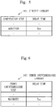
- Fig. 5 is a diagram illustrating the circuit library 182 according to the first embodiment by way of example.
- circuit library 182 according to the first embodiment will be described by way of example with reference to Fig. 5 .
- the circuit library 182 includes a computation identifier for identifying a type of the computation step and a delay time of the computation step per type of the computation step.
- the circuit library 182 includes a delay time (Xns) of the addition step.
- Fig. 6 is a diagram illustrating the error countermeasure library 183 according to the first embodiment by way of example.
- the error countermeasure library 183 according to the first embodiment will be described by way of example with reference to Fig. 6 .
- the error countermeasure library 183 includes a delay time (Yns) of the majority step.
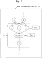
- Fig. 7 is a diagram illustrating the counter-error CDFG file 192 according to the first embodiment by way of example.
- the counter-error CDFG file 192 according to the first embodiment will be described by way of example with reference to Fig. 7 .
- the CDFG file 192 indicates a computation path Pn into which the notation of the majority step is inserted.
- the majority step is a step of selecting one computation result by majority when a plurality of different computation results are acquired.
- the majority step is an example of error countermeasure step.
- N is selected in the majority step.
- the computation path Pn includes the addition step and the majority step.
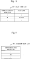
- Fig. 8 is a diagram illustrating the delay time list 193 according to the first embodiment by way of example.
- the delay time list 193 includes a computation path identifier for identifying a computation path graph and a counter-error delay time of the computation path per computation path graph.
- the inserted graph selection unit 121 generates the inserted graph list 194 as follows based on the target frequency 181 and the delay time list 193.
- the inserted graph selection unit 121 calculates a target time acquired by dividing unit time by the target frequency 181.
- the inserted graph selection unit 121 selects a computation path identifier associated with a delay time at the target time or less from among the computation path identifiers included in the delay time list 193.
- the computation path graph identified by the selected computation path identifier is an inserted path graph.
- the inserted graph selection unit 121 generates the inserted graph list 194 indicating each selected computation path identifier.
- the processing proceeds to S122 after S121.
- Fig. 9 is a diagram illustrating the inserted graph list 194 according to the first embodiment by way of example.
- the inserted graph list 194 according to the first embodiment will be described by way of example with reference to Fig. 9 .
- the inserted graph list 194 includes the computation path identifier of each inserted path graph.
- the computation path graph Pn is an inserted path graph.
- the error countermeasure insertion unit 122 selects an inserted path graph identified by a computation path identifier from the scheduled CDFG file 192 per computation path identifier included in the inserted graph list 194.
- the error countermeasure insertion unit 122 then inserts an error countermeasure notation into each selected inserted path graph.
- Fig. 10 is a diagram illustrating the counter-error CDFG file 192 according to the first embodiment by way of example.
- the bound CDFG file 192 includes information on hardware assigned to each step.
- the binding (hardware assignment) method may be the same method as performed in typical high-level synthesis.
- the processing proceeds to S 131 after S130.
- the RTL description output unit 131 converts the CDFG described in the bound CDFG file 192 into RTL description thereby to generate the RTL description file 195 denoting the RTL description therein.
- the method for converting CDFG into RTL description may be the same method as performed in typical high-level synthesis.
- the circuit design processing is terminated after S 131.
- Fig. 11 is a diagram illustrating an example of hardware structure of the circuit design device 100 according to the first embodiment.
- the circuit design device 100 is a computer including a computation device 901, an auxiliary storage device 902, a main storage device 903, a communication device 904, and an I/O device 905.
- the computation device 901, the auxiliary storage device 902, the main storage device 903, the communication device 904, and the I/O device 905 are connected to a bus 909.
- the auxiliary storage device 902 is ROM (Read Only Memory), flash memory, or hard disk device, for example.
- the main storage device 903 is RAM (Random Access Memory), for example.
- a program which is typically stored in the auxiliary storage device 902, is loaded into the main storage device 903, read by the computation device 901, and executed by the computation device 901.
- the operating system is stored in the auxiliary storage device 902.
- Programs for realizing the functions each described as a "unit” is stored in the auxiliary storage device 902.
- the OS and the programs for realizing the functions each described as the "unit” are loaded into the main storage device 903 and are executed by the computation device 901.
- the "unit” may be replaced with "processing,” “step,” “program,” or “device.”
- an error countermeasure notation can be inserted into CDFG such that a delay time does not exceed the target time.
- Fig. 12 is a functional structure diagram of the circuit design device 100 according to a second embodiment.
- circuit design device 100 The functional structure of the circuit design device 100 according to the second embodiment will be described with reference to Fig. 12 .
- the circuit design device 100 includes an inserted amount determination unit 123 in addition to the functions according to the first embodiment (see Fig. 1 ).
- the inserted amount determination unit 123 determines whether the amount of inserted error countermeasure notations reaches the target inserted amount 184 based on the number of inserted graphs inserting an error countermeasure notation therein.
- the target inserted amount 184 is a rate of the number of inserted graphs relative to the total number of computation path graphs (which will be denoted as insertion rate).
- the number of inserted graphs is the number of inserted graphs inserting an error countermeasure notation therein.
- the target inserted amount 184 may be other than the insertion rate.
- the target inserted amount 184 may be the number of inserted graphs inserting an error countermeasure notation therein.
- Fig. 13 is a flowchart illustrating a flow of circuit design processing of the circuit design device 100 according to the second embodiment.
- circuit design processing of the circuit design device 100 according to the second embodiment will be described with reference to Fig. 13 .
- the operation description input unit 110 acquires the operation description file 191.
- the CDFG generation unit 111 generates the CDFG file 192 from the operation description file 191.
- the scheduling unit 112 performs scheduling on the CDFG file 192.
- S110 to S 112 are the same as in the first embodiment (see Fig. 2 ).
- the delay time calculation unit 120 selects one unselected computation path graph from the scheduled CDFG file 192.
- the delay time calculation unit 120 then calculates a delay time of the selected computation path graph.
- the delay time calculation method is the same as in the first embodiment (see S120 in Fig. 2 ).
- the processing proceeds to S201 after S200.
- the inserted graph selection unit 121 compares the delay time calculated in S200 with the target time.
- the error countermeasure insertion unit 122 inserts an error countermeasure notation into the computation path graph (inserted path graph) selected in S200.
- the processing proceeds to S203 after S202.
- the inserted amount determination unit 123 calculates the amount of inserted error countermeasure notations.
- the inserted amount determination unit 123 then compares the amount of inserted error countermeasure notations with the target inserted amount 184.
- the delay time calculation unit 120 determines whether a computation path graph not selected in S200 is present.
- the processing proceeds to S130.
- the inserted amount determination unit 123 may display a message that the amount of inserted error countermeasure notations does not reach the target inserted amount 184.
- the binding unit 130 binds the counter-error CDFG file 192.
- the RTL description output unit 131 generates the RTL description file 195 from the bound CDFG file 192.
- S130 and S 131 are the same as in the first embodiment (see Fig. 2 ).
- the circuit design processing is terminated after S131.
- an error countermeasure notation can be inserted up to the target inserted amount 184. Thereby, it is possible to prevent the error countermeasure notations from being inserted more than needed, to limit the number of error countermeasure circuits, and to prevent an increase in area of the integrated circuit.
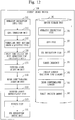
- Fig. 14 is a functional structure diagram of the circuit design device 100 according to a third embodiment.
- circuit design device 100 The functional structure of the circuit design device 100 according to the third embodiment will be described with reference to Fig. 14 .
- the circuit design device 100 includes a re-divided graph selection unit 124 and a division portion selection unit 125 in addition to the functions described according to the second embodiment (see Fig. 12 ).
- the re-divided graph selection unit 124 selects a computation path graph not inserting an error countermeasure notation therein from the scheduled CDFG file 192.
- a computation path graph selected by the re-divided graph selection unit 124 will be denoted as re-divided graph.
- the division portion selection unit 125 selects a division portion from a re-divided graph.
- the scheduling unit 112 divides a re-divided graph based on a division portion.
- Each graph, which is acquired by dividing a re-divided graph, will be denoted as subdivided graph, and a computation path indicated by a subdivided graph will be denoted as subdivided path.
- the delay time calculation unit 120 calculates a counter-error delay time of a subdivided path per subdivided graph.
- the inserted graph selection unit 121 selects an inserted graph from a plurality of subdivided graphs.
- a subdivided graph selected as inserted graph will be denoted as inserted subdivided graph.
- the error countermeasure insertion unit 122 inserts an error countermeasure notation into each inserted subdivided graph.
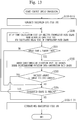
- Fig. 15 , Fig. 16 , and Fig. 17 are the flowcharts illustrating a flow of circuit design processing of the circuit design device 100 according to the third embodiment.
- circuit design processing of the circuit design device 100 according to the third embodiment will be described with reference to Fig. 15 to Fig. 17 .
- the re-divided graph selection unit 124 selects an unselected re-divided graph from the scheduled CDFG file 192.
- the re-divided graph selection unit 124 selects a computation path graph including a plurality of operators (a series of operators) arranged in series as re-divided graph from each computation path graph not inserting an error countermeasure notation therein.
- the processing proceeds to S211 after S210.
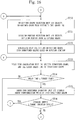
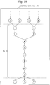
- Fig. 18 is a diagram illustrating the scheduled CDFG file 192 according to the third embodiment by way of example.
- the re-divided graph selection unit 124 selects a computation path graph Pa as unselected re-divided graph from the CDFG file 192 (see Fig. 18 ).
- the computation path graph Pa includes a plurality of operators (*, +1, +2) arranged in series.
- the division portion selection unit 125 selects a division portion from the re-divided graph selected in S210.
- the division portion selection unit 125 selects a division portion as follows from the re-divided graph Pa (see Fig. 18 ).
- the division portion selection unit 125 selects each operator (*, +1, +2) arranged in series as division portion.
- the division portion selection unit 125 selects an operator (*) using more variables than other operators as division portion from among the plurality of operators (*, +1, +2) arranged in series. That is, the division portion selection unit 125 selects a portion with more computation paths (including subdivided paths) as division portion. With the selection method, insertion efficiency of error countermeasure circuits is increased against an increase in latency (total steps required for computation).
- the division portion selection unit 125 selects an operator (+2) using more computation results than other operators as division portion from among the plurality of operators (*, +1, +2) arranged in series. That is, the division portion selection unit 125 selects a portion with more branches (fan-out) as division portion. With the selection method, an error countermeasure circuit is provided at a portion where a signal value is widely propagated, and thus the signal value of an error cannot be widely propagated.
- the processing proceeds to S212 after S211.
- the scheduling unit 112 divides the re-divided graph selected in S210 into a plurality of subdivided graphs based on the division portion selected in S211.
- a flip-flop is inserted between two subdivision paths arranged in series.
- the scheduling unit 112 divides the re-divided graph at each division portion immediately before (or after).
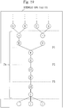
- Fig. 19 is a diagram illustrating the scheduled CDFG file 192 according to the third embodiment by way of example.
- the scheduling unit 112 divides the re-divided graph Pa (see Fig. 19 ) as follows.
- the scheduling unit 112 divides the re-divided graph Pa at the portion immediately before each operator (P1, P2, P3).
- the scheduling unit 112 divides the re-divided graph Pa at the portion (P1) immediately before the multiplication operator (*).
- the re-divided graph Pa is divided into three computation paths of A/B to E, C/D to F, and E/F to I.
- the re-divided graph Pa is branched into two computation paths of A/B/C/D to H and H to I. Therefore, the number of computation paths is larger for division at P1 than division at P3.
- the delay time calculation unit 120 then calculates a delay time of the selected subdivided graph.
- the delay time calculation method is the same as in the first embodiment (see S120 in Fig. 2 ).
- the inserted graph selection unit 121 compares the delay time calculated in S213 with the target time.
- the delay time calculation unit 120 determines whether a subdivided graph not selected in S213 is present.
- the re-divided graph selection unit 124 determines whether a re-divided graph not selected in S210 is present.
- the processing proceeds to S130.
- the inserted amount determination unit 123 may display a message that the amount of inserted error countermeasure notations does not reach the target inserted amount 184.
- S130 and S131 are the same as in the second embodiment (see Fig. 13 ).
- the circuit design processing is terminated after S131.
- an error countermeasure notation with the target inserted amount 184 can be inserted into the scheduled CDFG file 192 irrespective of the scheduled CDFG file 192.
- Fig. 20 is a functional structure diagram of the circuit design device 100 according to a fourth embodiment.
- circuit design device 100 The functional structure of the circuit design device 100 according to the fourth embodiment will be described with reference to Fig. 20 .
- the circuit design device 100 includes a graph group division unit 126 in addition to the functions described according to the first embodiment (see Fig. 1 ).
- the graph group division unit 126 divides a plurality of computation path graphs included in the CDFG indicated by the scheduled CDFG file 192 into a plurality of groups of path graphs.
- a group of path graphs is a plurality of consecutive computation path graphs (a series of computation path graphs).
- path graph quantity 185 The number of computation path graphs included in each group of path graphs will be denoted as path graph quantity 185.
- the delay time calculation unit 120 calculates a delay time per final path graph in each group of path graphs.
- the inserted graph selection unit 121 selects an inserted graph from the final path graph in each group of path graphs.
- Fig. 21 is a flowchart illustrating a flow of circuit design processing of the circuit design device 100 according to the fourth embodiment.
- circuit design processing of the circuit design device 100 according to the fourth embodiment will be described with reference to Fig. 21 .
- the circuit design processing includes S113 in addition to the processing described in the first embodiment (see Fig. 2 ).
- S110 to S 112 are the same as in the first embodiment.
- the graph group division unit 126 divides a plurality of computation path graphs included in the scheduled CDFG file 192 into a plurality of groups of path graphs based on the path graph quantity 185.
- the processing proceeds to S120 after S 113.
- the delay time calculation unit 120 generates the delay time list 193 based on the scheduled CDFG file 192 (similarly as in the first embodiment).
- the delay time calculation unit 120 calculates a delay time of the final computation path graph in each group of path graphs, not the delay times of all the computation path graphs. That is, the delay time list 193 indicates a delay time of the final computation path graph in each group of path graphs.
- the processing proceeds to S121 after S120.
- the inserted graph selection unit 121 generates the inserted graph list 194 based on the delay time list 193 (similarly as in the first embodiment).
- the processing proceeds to S122 after S121.
- the error countermeasure insertion unit 122 inserts an error countermeasure notation into each inserted graph based on the inserted graph list 194.
- the error countermeasure insertion unit 122 selects a group of path graphs including an inserted graph per inserted graph, and multiplexes a computation notation (such as operator) included in each computation path graph in each selected group of path graphs.
- the circuit design processing is terminated after S131.
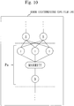
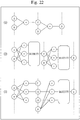
- Fig. 22 is an outline diagram of the error countermeasure insertion processing by the error countermeasure insertion unit 122 according to each embodiment.
- the error countermeasure insertion unit 122 inserts a majority circuit into both the first-half section and the second-half section.
- the error countermeasure insertion unit 122 further multiplexes an operator of each section.
- Fig. 23 is a functional structure diagram of the circuit design device 100 according to a fifth embodiment.
- circuit design device 100 The functional structure of the circuit design device 100 according to the fifth embodiment will be described with reference to Fig. 23 .
- the circuit design device 100 includes the graph group division unit 126 in addition to the functions described in the second embodiment (see Fig. 12 ).
- the function of the graph group division unit 126 is the same as in the fourth embodiment (see Fig. 20 ).
- the functions of the delay time calculation unit 120, the inserted graph selection unit 121, and the error countermeasure insertion units 122 are the same as in the fourth embodiment.
- Fig. 24 and Fig. 25 are the flowcharts illustrating a flow of circuit design processing of the circuit design device 100 according to the fifth embodiment.
- circuit design processing of the circuit design device 100 according to the fifth embodiment will be described with reference to Fig. 24 and Fig. 25 .
- S110 to S112 are the same as in the second embodiment (see Fig. 13 ).
- the graph group division unit 126 selects an unselected computation path graph not inserting an error countermeasure notation therein from the plurality of computation path graphs included in the scheduled CDFG file 192.
- the processing proceeds to S301 after S300.
- the graph group division unit 126 sets an initial value M for a variable N.
- the initial value M is the path graph quantity 185.
- the graph group division unit 126 subtracts 1 from the value of the variable N.
- the graph group division unit 126 determines whether the value of the variable N is 0.
- the graph group division unit 126 determines whether a computation path graph not selected in S300 is present.
- the delay time calculation unit 120 calculates a delay time of the final computation path graph included in the group of path graphs [N] determined in S302.
- the processing proceeds to S311 after S310.
- the inserted graph selection unit 121 compares the delay time calculated in S310 with the target time.
- the error countermeasure insertion unit 122 inserts an error countermeasure notation into the final computation path graph included in the group of path graphs [N] determined in S302.
- the error countermeasure insertion unit 122 multiplexes an operator included in each computation path graph in the group of path graphs [N].
- the inserted amount determination unit 123 calculates the amount of inserted error countermeasure notations, and compares the amount of inserted error countermeasure notations with the target inserted amount 184.
- the graph group division unit 126 may search a computation path while increasing N. In this case, the graph group division unit 126 sets 1 in N as the initial value in S301. Further, the graph group division unit 126 adds 1 to N in S303, and determines whether N is higher than M in S304.
- Fig. 26 is a diagram illustrating another example of functional structure of the circuit design device 100 according to the fifth embodiment.
- the circuit design device 100 includes the graph group division unit 126 in addition to the functions described in the third embodiment (see Fig. 14 ).
- the function of the graph group division unit 126 is the same as in the fourth embodiment (see Fig. 20 ).
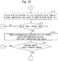
- Fig. 27 , Fig. 28 , Fig. 29 , and Fig. 30 are the flowcharts illustrating another example of circuit design processing of the circuit design device 100 according to the fifth embodiment.
- S302 when the group of path graphs [N] can be divided from the CDFG (YES), the processing proceeds to S310 (see Fig. 28 ).
- S310 to S313 are the same as in Fig. 25 .
- the circuit design processing is terminated after S131.
- the graph group division unit 126 may search a computation path while increasing N. That is, the graph group division unit 126 sets 1 in N as the initial value in S301, adds 1 to N in S303, and determines whether N is higher than M in S304.
- the circuit design device 100 may not include any of the components described according to each embodiment. Further, the circuit design device 100 may include a component not described according to each embodiment. Furthermore, the circuit design device 100 may be a combination of some or all of the components according to each embodiment.
- the processing procedure described in the flowcharts according to each embodiment is an example of method or program processing procedure according to each embodiment.
- the method and program according to each embodiment may be realized by a partially different processing procedure from the processing procedure described according to each embodiment.
- 100 Circuit design device, 110: Operation description input unit, 111: CDFG generation unit, 112: Scheduling unit, 120: Delay time calculation unit, 121: Inserted graph selection unit, 122: Error countermeasure insertion unit, 123: Inserted amount determination unit, 124: Re-divided graph selection unit, 125: Division portion selection unit, 126: Graph group division unit, 130: Binding unit, 131: RTL description output unit, 181: Target frequency, 182: Circuit library, 183: Error countermeasure library, 184: Target inserted amount, 185: Path graph quantity, 190: Device storage unit, 191: Operation description file, 192: CDFG file, 193: Delay time list, 194: Inserted graph list, 195: RTL description file, 901: Computation device, 902: Auxiliary storage device, 903: Main storage device, 904: Communication device, 905: I/O device, and 909: bus
Landscapes
- Engineering & Computer Science (AREA)
- Computer Hardware Design (AREA)
- Physics & Mathematics (AREA)
- Theoretical Computer Science (AREA)
- Evolutionary Computation (AREA)
- Geometry (AREA)
- General Engineering & Computer Science (AREA)
- General Physics & Mathematics (AREA)
- Design And Manufacture Of Integrated Circuits (AREA)
Abstract
A delay time calculation unit (120) calculates a delay time required to execute a computation path when an error countermeasure step is inserted into the computation path per computation path included in a scheduled CDFG file (192). An inserted graph selection unit (121) selects a computation path for which the delay time does not exceed a target time as inserted graph. An error countermeasure insertion unit (122) inserts an error countermeasure notation indicating the error countermeasure step into the inserted graph.
Description
- The present invention relates to a technique for designing an integrated circuit.
- As semiconductor integrated circuits become minute with lower voltage, influences by software errors, which are problematic in semiconductor integrated circuits for outer space, are increasing, and countermeasure against the software errors are emphasized also in the semiconductor integrated circuits for ground.
- There are widely known a method for duplexing a logic circuit and a method using triple modular redundancy (TMR) as countermeasure against the software errors.
- With the method for duplexing a logic circuit, the signal values of two logic circuits are compared thereby to detect an error of either of the signal values.
- With the method using TMR, one signal value is selected from the signal values of three logic circuits by majority thereby to correct an error of any signal value.
- However, when an error countermeasure circuit described above is added to a semiconductor integrated circuit designed in RTL description (RTL: register transfer level), a delay time in the semiconductor integrated circuit is further increased than when it is not subjected to the countermeasure, and an operable frequency (operation frequency) is lowered.
- On the other hand, there is a technique called high-level synthesis (
Patent Literature 1, for example) - With such a technique, RTL description including description of hardware such as arithmetic circuit or flip-flop is generated from operation description described in high-level language (such as SystemC) depending on a user-desired operation frequency.
- However, a method for enhancing reliability on software errors is not generally employed during high-level synthesis, and RTL with resistance to software errors cannot be generated from the operation description. Therefore, it is not possible to solve a problem that an operation frequency of a circuit is deteriorated when RTL after high-level synthesis is modified and double, triple logic circuit or the like is implemented.
-
- Patent Literature 1:
JP 2011-013823 A - Patent Literature 2:
JP 2010-257003 A - Patent Literature 3:
JP 2003-157294 A - It is an object of the present invention to enable an integrated circuit including an error countermeasure circuit and operating at a desired operation frequency to be designed.
- A circuit design device according to the present invention includes:
- a divided graph acquisition unit to acquire a plurality of divided graphs generated by dividing a control data flow graph indicating a control data flow of an integrated circuit;
- an execution time calculation unit to calculate an execution time required to execute a division flow when an error countermeasure step is inserted into the division flow indicated by a divided graph per divided graph among the plurality of divided graphs;
- an inserted graph selection unit to select a divided graph for which the execution time does not exceed a target time as inserted graph from among the plurality of divided graphs based on each execution time calculated by the execution time calculation unit; and
- an error countermeasure insertion unit to insert an error countermeasure notation indicating the error countermeasure step into the inserted graph selected by the inserted graph selection unit.
- According to the present invention, it is possible to insert an error countermeasure notation into a control data flow graph such that an execution time does not exceed a target time.
- Then, by use of the control data flow graph, it is possible to design an integrated circuit including an error countermeasure circuit and operating at a desired operation frequency.
-
-
Fig. 1 is a functional structure diagram of acircuit design device 100 according to a first embodiment. -
Fig. 2 is a flowchart illustrating a flow of circuit design processing of thecircuit design device 100 according to the first embodiment. -
Fig. 3 is a diagram illustrating aCDFG file 192 according to the first embodiment by way of example. -
Fig. 4 is a diagram illustrating the scheduledCDFG file 192 according to the first embodiment by way of example. -
Fig. 5 is a diagram illustrating acircuit library 182 according to the first embodiment by way of example. -
Fig. 6 is a diagram illustrating anerror countermeasure library 183 according to the first embodiment by way of example. -
Fig. 7 is a diagram illustrating thecounter-error CDFG file 192 according to the first embodiment by way of example. -
Fig. 8 is a diagram illustrating adelay time list 193 according to the first embodiment by way of example. -
Fig. 9 is a diagram illustrating an insertedgraph list 194 according to the first embodiment by way of example. -
Fig. 10 is a diagram illustrating thecounter-error CDFG file 192 according to the first embodiment by way of example. -
Fig. 11 is a diagram illustrating an example of hardware structure of thecircuit design device 100 according to the first embodiment. -
Fig. 12 is a functional structure diagram of thecircuit design device 100 according to a second embodiment. -
Fig. 13 is a flowchart illustrating a flow of circuit design processing of thecircuit design device 100 according to the second embodiment. -
Fig. 14 is a functional structure diagram of thecircuit design device 100 according to a third embodiment. -
Fig. 15 is a flowchart illustrating a flow of circuit design processing of thecircuit design device 100 according to the third embodiment. -
Fig. 16 is a flowchart illustrating a flow of circuit design processing of thecircuit design device 100 according to the third embodiment. -
Fig. 17 is a flowchart illustrating a flow of circuit design processing of thecircuit design device 100 according to the third embodiment. -
Fig. 18 is a diagram illustrating the scheduledCDFG file 192 according to the third embodiment by way of example. -
Fig. 19 is a diagram illustrating the scheduledCDFG file 192 according to the third embodiment by way of example. -
Fig. 20 is a functional structure diagram of thecircuit design device 100 according to a fourth embodiment. -
Fig. 21 is a flowchart illustrating a flow of circuit design processing of thecircuit design device 100 according to the fourth embodiment. -
Fig. 22 is an outline diagram of an error countermeasure insertion processing of an errorcountermeasure insertion unit 122 according to each embodiment. -
Fig. 23 is a functional structure diagram of thecircuit design device 100 according to a fifth embodiment. -
Fig. 24 is a flowchart illustrating a flow of circuit design processing of thecircuit design device 100 according to the fifth embodiment. -
Fig. 25 is a flowchart illustrating a flow of circuit design processing of thecircuit design device 100 according to the fifth embodiment. -
Fig. 26 is a diagram illustrating another example of functional structure of thecircuit design device 100 according to the fifth embodiment. -
Fig. 27 is a flowchart illustrating another example of circuit design processing of thecircuit design device 100 according to the fifth embodiment. -
Fig. 28 is a flowchart illustrating another example of circuit design processing of thecircuit design device 100 according to the fifth embodiment. -
Fig. 29 is a flowchart illustrating another example of circuit design processing of thecircuit design device 100 according to the fifth embodiment. -
Fig. 30 is a flowchart illustrating another example of circuit design processing of thecircuit design device 100 according to the fifth embodiment. - An embodiment for designing an integrated circuit including an error countermeasure circuit and operating at a desired operation frequency will be described.
-
Fig. 1 is a functional structure diagram of acircuit design device 100 according to a first embodiment. - The functional structure of the
circuit design device 100 according to the first embodiment will be described with reference toFig. 1 . - The
circuit design device 100 is a device that performs high-level synthesis for obtaining an RTLdescription file 195 from anoperation description file 191 of an integrated circuit. - The
operation description file 191 is an electronic file denoting the operation description of the integrated circuit therein. The operation description denotes the operations of the integrated circuit in HDL (hardware description language). SystemC is an example of HDL and high-level language. - The
RTL description file 195 is an electronic file denoting the RTL description of the integrated circuit therein. The RTL description denotes the operations of the integrated circuit in RTL (register transfer level). - The
circuit design device 100 includes an operationdescription input unit 110, aCDFG generation unit 111, and a scheduling unit 112 (an example of divided graph acquisition unit). - The
circuit design device 100 includes a delay time calculation unit 120 (an example of execution time calculation unit), an insertedgraph selection unit 121, and an errorcountermeasure insertion unit 122. - The
circuit design device 100 includes abinding unit 130, an RTLdescription output unit 131, and adevice storage unit 190. - The operation
description input unit 110 acquires theoperation description file 191. - The
CDFG generation unit 111 converts the operation description described in theoperation description file 191 into CDFG (control data flow graph) thereby to generate aCDFG file 192. - The
CDFG file 192 is an electronic file denoting the CDFG of the integrated circuit therein. The CDFG is a graph denoting a control data flow indicating a control flow of the integrated circuit and a data flow of the integrated circuit. - The
scheduling unit 112 determines an execution order of each computation step included in the control data flow indicated by the CDFG based on the CDFG described in theCDFG file 192. - The
scheduling unit 112 then divides the CDFG described in the CDFG file 192 into a plurality of graphs. - In the following, each graph acquired by dividing the CDFG by the
scheduling unit 112 will be denoted as computation path graph (an example of divided graph) and a control data flow indicated by a computation path graph will be denoted as computation path (an example of division flow). - Further, the CDFG file 192 processed by the
scheduling unit 112 will be denoted as scheduledCDFG file 192. - The scheduled
CDFG file 192 includes information on execution order of each computation step, identifier of each computation path, range of each computation path, and the like. - The delay
time calculation unit 120 calculates an execution time required to execute a computation path (which will be denoted as delay time below) when an error countermeasure step is inserted into the computation path indicated by a computation path graph per computation path graph described in the scheduledCDFG file 192. - A delay time calculated by the delay
time calculation unit 120 will be denoted as counter-error delay time. - The delay
time calculation unit 120 generates adelay time list 193 indicating a counter-error delay time of each computation path. - The inserted
graph selection unit 121 selects a computation path graph of a computation path for which the delay time does not exceed a target time from among a plurality of computation path graphs described in the scheduledCDFG file 192 based on thedelay time list 193. The target time is calculated by dividing unit time bytarget frequency 181. - A computation path graph selected by the inserted
graph selection unit 121 will be denoted as inserted graph, and a computation path indicated by an inserted graph will be denoted as insertion path. - The inserted
graph selection unit 121 generates an insertedgraph list 194 indicating an identifier of each selected inserted graph. - The error
countermeasure insertion unit 122 inserts an error countermeasure notation into each inserted graph based on the insertedgraph list 194. The error countermeasure notation indicates an error countermeasure circuit for performing the error countermeasure step. - The scheduled
CDFG file 192 processed by the errorcountermeasure insertion unit 122 will be denoted ascounter-error CDFG file 192. - The
binding unit 130 assigns hardware such as arithmetic circuit, flip-flop (FF) and error countermeasure circuit to each step included in the CDFG described in thecounter-error CDFG file 192. - The counter-error CDFG file 192 processed by the binding
unit 130 will be denoted asbound CDFG file 192 below. The boundCDFG file 192 includes information on hardware assigned to each step. - The RTL
description output unit 131 converts the CDFG described in the boundCDFG file 192 into RTL description thereby to generate theRTL description file 195. - The
device storage unit 190 stores data used, generated or input/output by thecircuit design device 100. - For example, the
device storage unit 190 stores theoperation description file 191, theCDFG file 192, thedelay time list 193, the insertedgraph list 194, and theRTL description file 195 therein. Thedevice storage unit 190 further stores thetarget frequency 181, a circuit library 182 (an example of execution time library), and anerror countermeasure library 183. - The
target frequency 181 is a target value of the operation frequency of the integrated circuit. A target time may be stored instead of thetarget frequency 181. - The
circuit library 182 is an electronic file including a delay time per computation step. - The
error countermeasure library 183 is an electronic file including a delay time per error countermeasure circuit (step). -
Fig. 2 is a flowchart illustrating a flow of circuit design processing of thecircuit design device 100 according to the first embodiment. - The circuit design processing of the
circuit design device 100 according to the first embodiment will be described with reference toFig. 2 . - In
S 110, a designer of the integrated circuit inputs theoperation description file 191 denoting the operation description of the integrated circuit therein into thecircuit design device 100. - The operation
description input unit 110 acquires the inputoperation description file 191. - The processing proceeds to S111 after S110.
- In S111, the
CDFG generation unit 111 converts the operation description of the integrated circuit described in theoperation description file 191 into CDFG thereby to generate the CDFG file 192 denoting the CDFG therein. - The CDFG includes CFG (control flow graph) and DFG (data flow graph).
- The CFG illustrates the processing branches such as if or while.
- The DFG illustrates a flow of data.
- The method for converting the operation description into CDFG may be the same method as performed in typical high-level synthesis.
- The processing proceeds to
S 112 after S111. -
Fig. 3 is a diagram illustrating the CDFG file 192 according to the first embodiment by way of example. - The
CDFG file 192 according to the first embodiment will be described by way of example with reference toFig. 3 . InFig. 3 , DFG is extracted from the CDFG indicated by theCDFG file 192. This is applicable to the following diagrams illustrating theCDFG file 192. - The CDFG described in the
CDFG file 192 includes the computation step of adding the value of a variable B to the value of a variable A. The value acquired by the addition is set as a variable D. - The computation step includes the notations of the variable A, the variable B, the addition, and the variable D.
- Retuning to
Fig. 2 , the description will be continued fromS 112. - In
S 112, thescheduling unit 112 performs the following scheduling on the CDFG file 192 based on thetarget frequency 181 and thecircuit library 182. - The
scheduling unit 112 determines an execution order of each computation step included in the control data flow indicated by the CDFG based on the CDFG described in theCDFG file 192. - The
scheduling unit 112 then divides the CDFG described in the CDFG file 192 into a plurality of computation path graphs. For example, the CDFG is divided before (or after) each operator. - A delay time of each computation path is a target time or less. The target time is calculated by dividing unit time (one second, for example) by the
target frequency 181. Further, a delay time of each computation step included in the CDFG is indicated in thecircuit library 182. - A flip-flop is inserted between two computation paths arranged in series.
- The scheduling method (determining an execution order and dividing CDFG) may be the same method as performed in typical high-level synthesis.
- The processing proceeds to S120 after S112.
-
Fig. 4 is a diagram illustrating the scheduledCDFG file 192 according to the first embodiment by way of example. - The scheduled
CDFG file 192 according to the first embodiment will be described by way of example with reference toFig. 4 . - The scheduled
CDFG file 192 includes a computation path identifier for identifying each computation path graph acquired by dividing the CDFG, and range information on a range of each computation path graph (in chained lines). A series of computation steps indicated between the two chained lines in the Figure is a computation path Pn. A flip-flop is inserted in the portion indicated by a chained line in the Figure. - The computation path Pn is a computation step in which a value obtained by adding the value of the variable B to the value of the variable A is set for the variable D. The flip-flops are inserted before and after the computation path Pn.
- Returning to
Fig. 2 , the description will be continued from S120. - In S120, the delay
time calculation unit 120 generates thedelay time list 193 as follows based on thecircuit library 182, theerror countermeasure library 183, and the scheduledCDFG file 192. - The delay
time calculation unit 120 calculates a counter-error delay time of a computation path per computation path graph described in the scheduledCDFG file 192. - The delay
time calculation unit 120 generates thedelay time list 193 indicating a counter-error delay time of each computation path. - The delay time of each computation step included in the CDFG is indicated in the
circuit library 182. The delay time of the error countermeasure step is indicated in theerror countermeasure library 183. - The designer may designate a type of the error countermeasure step (such as duplex, triple, or majority) for the
circuit design device 100. - In this case, the
error countermeasure library 183 indicates a delay time of the error countermeasure step per type of the error countermeasure step. The delaytime calculation unit 120 then acquires a delay time of the error countermeasure step of a type designated by the designer from theerror countermeasure library 183, and calculates a counter-error delay time by use of the acquired delay time. - The processing proceeds to
S 121 after S120. -
Fig. 5 is a diagram illustrating thecircuit library 182 according to the first embodiment by way of example. - The
circuit library 182 according to the first embodiment will be described by way of example with reference toFig. 5 . - The
circuit library 182 includes a computation identifier for identifying a type of the computation step and a delay time of the computation step per type of the computation step. - For example, the
circuit library 182 includes a delay time (Xns) of the addition step. -
Fig. 6 is a diagram illustrating theerror countermeasure library 183 according to the first embodiment by way of example. - The
error countermeasure library 183 according to the first embodiment will be described by way of example with reference toFig. 6 . - The
error countermeasure library 183 includes an error countermeasure identifier for identifying a type of the error countermeasure step and a delay time of the error countermeasure step per type of the error countermeasure step. - For example, the
error countermeasure library 183 includes a delay time (Yns) of the majority step. -
Fig. 7 is a diagram illustrating the counter-error CDFG file 192 according to the first embodiment by way of example. - The counter-error CDFG file 192 according to the first embodiment will be described by way of example with reference to
Fig. 7 . - The
CDFG file 192 indicates a computation path Pn into which the notation of the majority step is inserted. - The majority step is a step of selecting one computation result by majority when a plurality of different computation results are acquired. The majority step is an example of error countermeasure step.
- Assuming that two computation results are N and one computation result is N', N is selected in the majority step.
- The computation path Pn includes the addition step and the majority step.
- Assuming that the delay time of the addition step is Xns and the delay time of the majority step is Yns, the counter-error delay time of the computation path Pn is Xns + Yns.
-
Fig. 8 is a diagram illustrating thedelay time list 193 according to the first embodiment by way of example. - The
delay time list 193 according to the first embodiment will be described by way of example with reference toFig. 8 . - The
delay time list 193 includes a computation path identifier for identifying a computation path graph and a counter-error delay time of the computation path per computation path graph. - For example, the
delay time list 193 includes the delay time (Xns + Yns) of the computation path Pn. - Returning to
Fig. 2 , the description will be continued from S121. - In S121, the inserted
graph selection unit 121 generates the insertedgraph list 194 as follows based on thetarget frequency 181 and thedelay time list 193. - The inserted
graph selection unit 121 calculates a target time acquired by dividing unit time by thetarget frequency 181. - The inserted
graph selection unit 121 selects a computation path identifier associated with a delay time at the target time or less from among the computation path identifiers included in thedelay time list 193. The computation path graph identified by the selected computation path identifier is an inserted path graph. - The inserted
graph selection unit 121 generates the insertedgraph list 194 indicating each selected computation path identifier. - The processing proceeds to S122 after S121.
-
Fig. 9 is a diagram illustrating the insertedgraph list 194 according to the first embodiment by way of example. - The inserted
graph list 194 according to the first embodiment will be described by way of example with reference toFig. 9 . - The inserted
graph list 194 includes the computation path identifier of each inserted path graph. - For example, the computation path graph Pn is an inserted path graph.
- Returning to
Fig. 2 , the description will be continued from S122. - In S122, the error
countermeasure insertion unit 122 selects an inserted path graph identified by a computation path identifier from the scheduled CDFG file 192 per computation path identifier included in the insertedgraph list 194. - The error
countermeasure insertion unit 122 then inserts an error countermeasure notation into each selected inserted path graph. - The processing proceeds to S130 after S122.
-
Fig. 10 is a diagram illustrating the counter-error CDFG file 192 according to the first embodiment by way of example. - For example, the error
countermeasure insertion unit 122 multiplexes the addition notation included in the inserted path graph Pn in the scheduled CDFG file 192 (Fig. 4 ) to be triple. The errorcountermeasure insertion unit 122 then inserts the notation of the majority step connected to the three addition notations thereby to generate the CDFG file 192 as illustrated inFig. 10 . - Returning to
Fig. 2 , the description will be continued from S130. - In S130, the binding
unit 130 assigns hardware such as arithmetic circuit, flip-flop, and error countermeasure circuit to each step included in the CDFG described in thecounter-error CDFG file 192. - The bound
CDFG file 192 includes information on hardware assigned to each step. - The binding (hardware assignment) method may be the same method as performed in typical high-level synthesis.
- The processing proceeds to
S 131 after S130. - In
S 131, the RTLdescription output unit 131 converts the CDFG described in the boundCDFG file 192 into RTL description thereby to generate theRTL description file 195 denoting the RTL description therein. - The method for converting CDFG into RTL description may be the same method as performed in typical high-level synthesis.
- The circuit design processing is terminated after
S 131. -
Fig. 11 is a diagram illustrating an example of hardware structure of thecircuit design device 100 according to the first embodiment. - The hardware structure of the
circuit design device 100 according to the first embodiment will be described by way of example with reference toFig. 11 . The hardware structure of thecircuit design device 100 maybe different from the structure illustrated inFig. 11 . - The
circuit design device 100 is a computer including acomputation device 901, anauxiliary storage device 902, amain storage device 903, acommunication device 904, and an I/O device 905. - The
computation device 901, theauxiliary storage device 902, themain storage device 903, thecommunication device 904, and the I/O device 905 are connected to a bus 909. - The
computation device 901 is CPU (Central Processing Unit) for executing a program - The
auxiliary storage device 902 is ROM (Read Only Memory), flash memory, or hard disk device, for example. - The
main storage device 903 is RAM (Random Access Memory), for example. - The
communication device 904 makes communication via Internet, LAN (Local Area Network), telephone line network, or other networks in a wired or wireless manner. - The I/
O device 905 is mouse, keyboard, or display device, for example. - A program, which is typically stored in the
auxiliary storage device 902, is loaded into themain storage device 903, read by thecomputation device 901, and executed by thecomputation device 901. - For example, the operating system (OS) is stored in the
auxiliary storage device 902. Further, Programs for realizing the functions each described as a "unit" is stored in theauxiliary storage device 902. Then, the OS and the programs for realizing the functions each described as the "unit" are loaded into themain storage device 903 and are executed by thecomputation device 901. The "unit" may be replaced with "processing," "step," "program," or "device." - Information, data, files, signal values or variable values indicating results of processing such as "determination," "judgement," "extraction," "detection," "setting," "registration," "selection", "generation," "input," "output," and the like are stored in the
main storage device 903 or theauxiliary storage device 902. - According to the first embodiment, an error countermeasure notation can be inserted into CDFG such that a delay time does not exceed the target time.
- By use of the CDFG, it is possible to design an integrated circuit including the error countermeasure circuit and operating at the
target frequency 181. - An embodiment for inserting an error countermeasure notation up to the target inserted amount will be described.
- The different points from the first embodiment will be mainly described below. The points, which are not described, are the same as in the first embodiment.
-
Fig. 12 is a functional structure diagram of thecircuit design device 100 according to a second embodiment. - The functional structure of the
circuit design device 100 according to the second embodiment will be described with reference toFig. 12 . - The
circuit design device 100 includes an insertedamount determination unit 123 in addition to the functions according to the first embodiment (seeFig. 1 ). - The inserted
amount determination unit 123 determines whether the amount of inserted error countermeasure notations reaches the target insertedamount 184 based on the number of inserted graphs inserting an error countermeasure notation therein. - For example, the target inserted
amount 184 is a rate of the number of inserted graphs relative to the total number of computation path graphs (which will be denoted as insertion rate). The number of inserted graphs is the number of inserted graphs inserting an error countermeasure notation therein. - The target inserted
amount 184 may be other than the insertion rate. For example, the target insertedamount 184 may be the number of inserted graphs inserting an error countermeasure notation therein. -
Fig. 13 is a flowchart illustrating a flow of circuit design processing of thecircuit design device 100 according to the second embodiment. - The circuit design processing of the
circuit design device 100 according to the second embodiment will be described with reference toFig. 13 . - In S110, the operation
description input unit 110 acquires theoperation description file 191. - In S111, the
CDFG generation unit 111 generates the CDFG file 192 from theoperation description file 191. - In S12, the
scheduling unit 112 performs scheduling on theCDFG file 192. - S110 to
S 112 are the same as in the first embodiment (seeFig. 2 ). - The processing proceeds to S200 after S112.
- In S200, the delay
time calculation unit 120 selects one unselected computation path graph from the scheduledCDFG file 192. - The delay
time calculation unit 120 then calculates a delay time of the selected computation path graph. The delay time calculation method is the same as in the first embodiment (see S120 inFig. 2 ). - The processing proceeds to S201 after S200.
- In S201, the inserted
graph selection unit 121 compares the delay time calculated in S200 with the target time. - When the delay time is the target time or less (YES), the processing proceeds to S202.
- When the delay time is longer than the target time (NO), the processing proceeds to S204.
- In S202, the error
countermeasure insertion unit 122 inserts an error countermeasure notation into the computation path graph (inserted path graph) selected in S200. - The processing proceeds to S203 after S202.
- In S203, the inserted
amount determination unit 123 calculates the amount of inserted error countermeasure notations. - The inserted
amount determination unit 123 then compares the amount of inserted error countermeasure notations with the target insertedamount 184. - When the amount of inserted error countermeasure notations is the target inserted
amount 184 or more (YES), the processing proceeds to S130. - When the amount of inserted error countermeasure notations is less than the target inserted amount 184 (NO), the processing proceeds to S204.
- In S204, the delay
time calculation unit 120 determines whether a computation path graph not selected in S200 is present. - When an unselected computation path graph is present (YES), the processing returns to S200.
- When an unselected computation path graph is not present (NO), the processing proceeds to S130. In this case, the inserted
amount determination unit 123 may display a message that the amount of inserted error countermeasure notations does not reach the target insertedamount 184. - In S130, the binding
unit 130 binds thecounter-error CDFG file 192. - In S131, the RTL
description output unit 131 generates theRTL description file 195 from the boundCDFG file 192. - S130 and
S 131 are the same as in the first embodiment (seeFig. 2 ). - The circuit design processing is terminated after S131.
- According to the second embodiment, an error countermeasure notation can be inserted up to the target inserted
amount 184. Thereby, it is possible to prevent the error countermeasure notations from being inserted more than needed, to limit the number of error countermeasure circuits, and to prevent an increase in area of the integrated circuit. - An embodiment when the amount of inserted error countermeasure notations does not reach the target inserted
amount 184 will be described. - The different points from the second embodiment will be mainly described below. The points, which are not described, are the same as in the second embodiment.
-
Fig. 14 is a functional structure diagram of thecircuit design device 100 according to a third embodiment. - The functional structure of the
circuit design device 100 according to the third embodiment will be described with reference toFig. 14 . - The
circuit design device 100 includes a re-dividedgraph selection unit 124 and a divisionportion selection unit 125 in addition to the functions described according to the second embodiment (seeFig. 12 ). - When the amount of inserted error countermeasure notations does not reach the target inserted
amount 184, the re-dividedgraph selection unit 124 selects a computation path graph not inserting an error countermeasure notation therein from the scheduledCDFG file 192. A computation path graph selected by the re-dividedgraph selection unit 124 will be denoted as re-divided graph. - The division
portion selection unit 125 selects a division portion from a re-divided graph. - The
scheduling unit 112 divides a re-divided graph based on a division portion. Each graph, which is acquired by dividing a re-divided graph, will be denoted as subdivided graph, and a computation path indicated by a subdivided graph will be denoted as subdivided path. - The delay
time calculation unit 120 calculates a counter-error delay time of a subdivided path per subdivided graph. - The inserted
graph selection unit 121 selects an inserted graph from a plurality of subdivided graphs. A subdivided graph selected as inserted graph will be denoted as inserted subdivided graph. - The error
countermeasure insertion unit 122 inserts an error countermeasure notation into each inserted subdivided graph. -
Fig. 15 ,Fig. 16 , andFig. 17 are the flowcharts illustrating a flow of circuit design processing of thecircuit design device 100 according to the third embodiment. - The circuit design processing of the
circuit design device 100 according to the third embodiment will be described with reference toFig. 15 to Fig. 17 . - S110 to S204 (see
Fig. 15 ) are the same as in the second embodiment (seeFig. 13 ). - In S204, when an unselected computation path graph is not present (NO), the processing proceeds to S210 (see
Fig. 16 ). - In S210 (see
Fig. 16 ), the re-dividedgraph selection unit 124 selects an unselected re-divided graph from the scheduledCDFG file 192. - For example, the re-divided
graph selection unit 124 selects a computation path graph including a plurality of operators (a series of operators) arranged in series as re-divided graph from each computation path graph not inserting an error countermeasure notation therein. - The processing proceeds to S211 after S210.
-
Fig. 18 is a diagram illustrating the scheduledCDFG file 192 according to the third embodiment by way of example, - For example, the re-divided
graph selection unit 124 selects a computation path graph Pa as unselected re-divided graph from the CDFG file 192 (seeFig. 18 ). - The computation path graph Pa includes a plurality of operators (*, +1, +2) arranged in series.
- Returning to
Fig. 16 , the description will be continued from S211. - In S211, the division
portion selection unit 125 selects a division portion from the re-divided graph selected in S210. - For example, the division
portion selection unit 125 selects a division portion as follows from the re-divided graph Pa (seeFig. 18 ). - The division
portion selection unit 125 selects each operator (*, +1, +2) arranged in series as division portion. - The division
portion selection unit 125 selects an operator (*) using more variables than other operators as division portion from among the plurality of operators (*, +1, +2) arranged in series. That is, the divisionportion selection unit 125 selects a portion with more computation paths (including subdivided paths) as division portion. With the selection method, insertion efficiency of error countermeasure circuits is increased against an increase in latency (total steps required for computation). - The division
portion selection unit 125 selects an operator (+2) using more computation results than other operators as division portion from among the plurality of operators (*, +1, +2) arranged in series. That is, the divisionportion selection unit 125 selects a portion with more branches (fan-out) as division portion. With the selection method, an error countermeasure circuit is provided at a portion where a signal value is widely propagated, and thus the signal value of an error cannot be widely propagated. - The processing proceeds to S212 after S211.
- In S212, the
scheduling unit 112 divides the re-divided graph selected in S210 into a plurality of subdivided graphs based on the division portion selected in S211. A flip-flop is inserted between two subdivision paths arranged in series. - For example, the
scheduling unit 112 divides the re-divided graph at each division portion immediately before (or after). - The processing proceeds to S213 after S212.
-
Fig. 19 is a diagram illustrating the scheduledCDFG file 192 according to the third embodiment by way of example. - For example, the
scheduling unit 112 divides the re-divided graph Pa (seeFig. 19 ) as follows. - When the three operators (*, +1, +2) are selected as division portions, the
scheduling unit 112 divides the re-divided graph Pa at the portion immediately before each operator (P1, P2, P3). - When the multiplication operator (*) is selected as division portion, the
scheduling unit 112 divides the re-divided graph Pa at the portion (P1) immediately before the multiplication operator (*). When division is made at P1, the re-divided graph Pa is divided into three computation paths of A/B to E, C/D to F, and E/F to I. On the other hand, when division is made at P3, the re-divided graph Pa is branched into two computation paths of A/B/C/D to H and H to I. Therefore, the number of computation paths is larger for division at P1 than division at P3. - When the operator (+2) for adding 2 is selected as division portion, the
scheduling unit 112 divides the re-divided graph Pa at the portion (P3) immediately before the operator (+2). When division is made at P3, the number of branches from a variable I behind P3 is three. On the other hand, when division is made at P1, the number of branches from a variable G behind P1 is 1. Therefore, the number of branches is larger for division at P3 than division at P1. - Returning to
Fig. 16 , the description will be continued from S213. - In S213, the delay
time calculation unit 120 selects an unselected subdivided graph from the plurality of subdivided graphs acquired in S212. - The delay
time calculation unit 120 then calculates a delay time of the selected subdivided graph. The delay time calculation method is the same as in the first embodiment (see S120 inFig. 2 ). - The processing proceeds to S214 after S213.
- In S214, the inserted
graph selection unit 121 compares the delay time calculated in S213 with the target time. - When the delay time is the target time or less (YES), the processing proceeds to S215.
- When the delay time is longer than the target time (NO), the processing proceeds to S217 (see
Fig. 17 ). - In S215, the error
countermeasure insertion unit 122 inserts an error countermeasure notation into the subdivided graph selected in S213. - The processing proceeds to S216 after S215.
- In S216, the inserted
amount determination unit 123 calculates the amount of inserted error countermeasure notations. - The inserted
amount determination unit 123 then compares the amount of inserted error countermeasure notations with the target insertedamount 184. - When the amount of inserted error countermeasure notations is the target inserted
amount 184 or more (YES), the processing proceeds to S 130 (seeFig. 17 ). - When the amount of inserted error countermeasure notations is less than the target inserted amount 184 (NO), the processing proceeds to S217 (see
Fig. 17 ). - In S217 (see
Fig. 17 ), the delaytime calculation unit 120 determines whether a subdivided graph not selected in S213 is present. - When an unselected subdivided graph is present (YES), the processing returns to S213.
- When an unselected subdivided graph is not present (NO), the processing proceeds to S218.
- In S218, the re-divided
graph selection unit 124 determines whether a re-divided graph not selected in S210 is present. - When an unselected re-divided graph is present (YES), the processing returns to S210.
- When an unselected re-divided graph is not present (NO), the processing proceeds to S130. In this case, the inserted
amount determination unit 123 may display a message that the amount of inserted error countermeasure notations does not reach the target insertedamount 184. - S130 and S131 are the same as in the second embodiment (see
Fig. 13 ). - The circuit design processing is terminated after S131.
- According to the third embodiment, an error countermeasure notation with the target inserted
amount 184 can be inserted into the scheduledCDFG file 192 irrespective of the scheduledCDFG file 192. - An embodiment for inserting an error countermeasure notation per group of computation paths, not per computation path, will be described.
- The different points from the first embodiment will be mainly described below. The points, which are not described, are the same as in the first embodiment.
-
Fig. 20 is a functional structure diagram of thecircuit design device 100 according to a fourth embodiment. - The functional structure of the
circuit design device 100 according to the fourth embodiment will be described with reference toFig. 20 . - The
circuit design device 100 includes a graphgroup division unit 126 in addition to the functions described according to the first embodiment (seeFig. 1 ). - The graph
group division unit 126 divides a plurality of computation path graphs included in the CDFG indicated by the scheduledCDFG file 192 into a plurality of groups of path graphs. A group of path graphs is a plurality of consecutive computation path graphs (a series of computation path graphs). - The number of computation path graphs included in each group of path graphs will be denoted as
path graph quantity 185. - The delay
time calculation unit 120 calculates a delay time per final path graph in each group of path graphs. - The inserted
graph selection unit 121 selects an inserted graph from the final path graph in each group of path graphs. -
Fig. 21 is a flowchart illustrating a flow of circuit design processing of thecircuit design device 100 according to the fourth embodiment. - The circuit design processing of the
circuit design device 100 according to the fourth embodiment will be described with reference toFig. 21 . - The circuit design processing includes S113 in addition to the processing described in the first embodiment (see
Fig. 2 ). - S110 to
S 112 are the same as in the first embodiment. - The processing proceeds to
S 113 afterS 112. - In S113, the graph
group division unit 126 divides a plurality of computation path graphs included in the scheduledCDFG file 192 into a plurality of groups of path graphs based on thepath graph quantity 185. - The processing proceeds to S120 after
S 113. - In S120, the delay
time calculation unit 120 generates thedelay time list 193 based on the scheduled CDFG file 192 (similarly as in the first embodiment). - The delay
time calculation unit 120 calculates a delay time of the final computation path graph in each group of path graphs, not the delay times of all the computation path graphs. That is, thedelay time list 193 indicates a delay time of the final computation path graph in each group of path graphs. - The processing proceeds to S121 after S120.
- In S121, the inserted
graph selection unit 121 generates the insertedgraph list 194 based on the delay time list 193 (similarly as in the first embodiment). - The processing proceeds to S122 after S121.
- In S122, the error
countermeasure insertion unit 122 inserts an error countermeasure notation into each inserted graph based on the insertedgraph list 194. - Further, the error
countermeasure insertion unit 122 selects a group of path graphs including an inserted graph per inserted graph, and multiplexes a computation notation (such as operator) included in each computation path graph in each selected group of path graphs. - The processing proceeds to S130 after S122.
- S130 and
S 131 are the same as in the first embodiment. - The circuit design processing is terminated after S131.
-
Fig. 22 is an outline diagram of the error countermeasure insertion processing by the errorcountermeasure insertion unit 122 according to each embodiment. - An outline of the error countermeasure insertion processing by the error
countermeasure insertion unit 122 according to each embodiment will be described with reference toFig. 22 . - (1) of
Fig. 22 is DFG before the error countermeasure circuit is inserted. - In (2) of
Fig. 22 , the errorcountermeasure insertion unit 122 inserts a majority circuit into both the first-half section and the second-half section. The errorcountermeasure insertion unit 122 further multiplexes an operator of each section. - In (3) of
Fig. 22 , it is assumed that a delay in the first-half section in which the delay of the adder and the delay of the majority circuit are summed is larger than the target delay. In this case, the errorcountermeasure insertion unit 122 cannot insert the majority circuit into the first-half section. Thus, the errorcountermeasure insertion unit 122 multiplexes an operator of the first-half section without inserting the majority circuit into the first-half section. The errorcountermeasure insertion unit 122 then inserts the majority circuit into the second-half section thereby to multiplex an operator of the second-half section. Thereby, even when the majority circuit cannot be inserted into the first-half section, a countermeasure against errors is enabled. - An embodiment for inserting an error countermeasure notation per group of computation paths not per computation path will be described.
- The different points from the second and third embodiments will be mainly described below. The points, which are not described, are the same as in the second and third embodiments.
-
Fig. 23 is a functional structure diagram of thecircuit design device 100 according to a fifth embodiment. - The functional structure of the
circuit design device 100 according to the fifth embodiment will be described with reference toFig. 23 . - The
circuit design device 100 includes the graphgroup division unit 126 in addition to the functions described in the second embodiment (seeFig. 12 ). - The function of the graph
group division unit 126 is the same as in the fourth embodiment (seeFig. 20 ). - The functions of the delay
time calculation unit 120, the insertedgraph selection unit 121, and the errorcountermeasure insertion units 122 are the same as in the fourth embodiment. -
Fig. 24 andFig. 25 are the flowcharts illustrating a flow of circuit design processing of thecircuit design device 100 according to the fifth embodiment. - The circuit design processing of the
circuit design device 100 according to the fifth embodiment will be described with reference toFig. 24 andFig. 25 . - S110 to S112 (see
Fig. 24 ) are the same as in the second embodiment (seeFig. 13 ). - The processing proceeds to S300 after S112.
- In S300, the graph
group division unit 126 selects an unselected computation path graph not inserting an error countermeasure notation therein from the plurality of computation path graphs included in the scheduledCDFG file 192. - The processing proceeds to S301 after S300.
- In S301, the graph
group division unit 126 sets an initial value M for a variable N. The initial value M is thepath graph quantity 185. - The processing proceeds to S302 after S301.
- In S302, the graph
group division unit 126 determines whether a computation path graph inserting an error countermeasure notation therein is included in N computation path graphs consecutive from the computation path graph selected in S300. N consecutive computation path graphs will be denoted as a group of path graphs [N] below. A group of path graphs [N] not including a computation path graph inserting an error countermeasure notation therein can be divided from the CDFG - When the group of path graphs [N] can be divided from the CDFG (YES), the processing proceeds to S310 (see
Fig. 25 ). - When the group of path graphs [N] cannot be divided from the CDFG (NO), the processing proceeds to S303.
- In S303, the graph
group division unit 126 subtracts 1 from the value of the variable N. - The processing proceeds to S304 after S303.
- In S304, the graph
group division unit 126 determines whether the value of the variable N is 0. - When the value of the variable N is 0 (YES), the processing proceeds to S305.
- When the value of the variable N is not 0 (NO), the processing returns to S302.
- In S305, the graph
group division unit 126 determines whether a computation path graph not selected in S300 is present. - When an unselected computation path graph is present (YES), the processing returns to S300.
- When an unselected computation path graph is not present (NO), the processing proceeds to S130 (see
Fig. 25 ). - In S310 (see
Fig. 25 ), the delaytime calculation unit 120 calculates a delay time of the final computation path graph included in the group of path graphs [N] determined in S302. - The processing proceeds to S311 after S310.
- In S311, the inserted
graph selection unit 121 compares the delay time calculated in S310 with the target time. - When the delay time is the target time or less (YES), the processing proceeds to S312.
- When the delay time is longer than the target time (NO), the processing proceeds to S303 (see
Fig. 24 ). - In S312, the error
countermeasure insertion unit 122 inserts an error countermeasure notation into the final computation path graph included in the group of path graphs [N] determined in S302. - Further, the error
countermeasure insertion unit 122 multiplexes an operator included in each computation path graph in the group of path graphs [N]. - The processing proceeds to S313 after S312.
- In S313, the inserted
amount determination unit 123 calculates the amount of inserted error countermeasure notations, and compares the amount of inserted error countermeasure notations with the target insertedamount 184. - When the amount of inserted error countermeasure notations is the target inserted
amount 184 or more (YES), the processing proceeds to S130. - When the amount of inserted error countermeasure notations is less than the target inserted amount 184 (NO), the processing proceeds to S305 (see
Fig. 24 ). - S130 and
S 131 are the same as in the second embodiment (seeFig. 13 ). - The circuit design processing is terminated after S131.
- As described above, the graph
group division unit 126 searches a computation path into which an error countermeasure notation can be inserted while subtracting the number of computation path graphs N included in the group of path graphs [N] from the number of path graphs M. - The graph
group division unit 126 may search a computation path while increasing N. In this case, the graphgroup division unit 126sets 1 in N as the initial value in S301. Further, the graphgroup division unit 126 adds 1 to N in S303, and determines whether N is higher than M in S304. -
Fig. 26 is a diagram illustrating another example of functional structure of thecircuit design device 100 according to the fifth embodiment. - Other example of functional structures of the
circuit design device 100 according to the fifth embodiment will be described with reference toFig. 26 . - The
circuit design device 100 includes the graphgroup division unit 126 in addition to the functions described in the third embodiment (seeFig. 14 ). - The function of the graph
group division unit 126 is the same as in the fourth embodiment (seeFig. 20 ). - The functions of the delay
time calculation unit 120, the insertedgraph selection unit 121, and the errorcountermeasure insertion unit 122 are the same as in the fourth embodiment. -
Fig. 27 ,Fig. 28 ,Fig. 29 , andFig. 30 are the flowcharts illustrating another example of circuit design processing of thecircuit design device 100 according to the fifth embodiment. - A series of other example of circuit design processing of the
circuit design device 100 according to the fifth embodiment will be described with reference toFig. 27 to Fig. 30 . - S110 to S305 (see
Fig. 27 ) are the same as inFig. 24 . - In S302, when the group of path graphs [N] can be divided from the CDFG (YES), the processing proceeds to S310 (see
Fig. 28 ). S310 to S313 (seeFig. 28 ) are the same as inFig. 25 . - In S305, when an unselected computation path graph is not present (NO), the processing proceeds to S210 (see
Fig. 29 ). - S210 to S216 (see
Fig. 29 ) are the same as inFig. 16 . - In S216, when the amount of inserted error countermeasure notations is less than the target inserted amount 184 (NO), the processing proceeds to S217 (see
Fig. 30 ). - S217, S218, S130, and S131 (see
Fig. 30 ) are the same as inFig. 17 . - The circuit design processing is terminated after S131.
- As in
Fig. 24 , the graphgroup division unit 126 may search a computation path while increasing N. That is, the graphgroup division unit 126sets 1 in N as the initial value in S301, adds 1 to N in S303, and determines whether N is higher than M in S304. - According to the fifth embodiment, it is possible to insert an error countermeasure notation per group of computation paths.
- Each embodiment is an example of embodiment of the
circuit design device 100. - That is, the
circuit design device 100 may not include any of the components described according to each embodiment. Further, thecircuit design device 100 may include a component not described according to each embodiment. Furthermore, thecircuit design device 100 may be a combination of some or all of the components according to each embodiment. - The
circuit design device 100 may be configured in one device (casing) or may be configured in a plurality of devices (systems). - The processing procedure described in the flowcharts according to each embodiment is an example of method or program processing procedure according to each embodiment. The method and program according to each embodiment may be realized by a partially different processing procedure from the processing procedure described according to each embodiment.
- 100: Circuit design device, 110: Operation description input unit, 111: CDFG generation unit, 112: Scheduling unit, 120: Delay time calculation unit, 121: Inserted graph selection unit, 122: Error countermeasure insertion unit, 123: Inserted amount determination unit, 124: Re-divided graph selection unit, 125: Division portion selection unit, 126: Graph group division unit, 130: Binding unit, 131: RTL description output unit, 181: Target frequency, 182: Circuit library, 183: Error countermeasure library, 184: Target inserted amount, 185: Path graph quantity, 190: Device storage unit, 191: Operation description file, 192: CDFG file, 193: Delay time list, 194: Inserted graph list, 195: RTL description file, 901: Computation device, 902: Auxiliary storage device, 903: Main storage device, 904: Communication device, 905: I/O device, and 909: bus
Claims (9)
- A circuit design device comprising:a divided graph acquisition unit to acquire a plurality of divided graphs generated by dividing a control data flow graph indicating a control data flow of an integrated circuit;an execution time calculation unit to calculate an execution time required to execute a division flow when an error countermeasure step is inserted into the division flow indicated by a divided graph per divided graph among the plurality of divided graphs;an inserted graph selection unit to select a divided graph for which the execution time does not exceed a target time, as inserted graph, from among the plurality of divided graphs based on each execution time calculated by the execution time calculation unit; andan error countermeasure insertion unit to insert an error countermeasure notation indicating the error countermeasure step into the inserted graph selected by the inserted graph selection unit.
- The circuit design device according to claim 1,
wherein the execution time calculation unit calculates the execution time of each divided graph based on an execution time library including an execution time required to execute each step included in the control data flow, and an execution time required to execute an error countermeasure step. - The circuit design device according to claim 1, comprising:an inserted amount determination unit,wherein the inserted amount determination unit determines whether the amount of inserted error countermeasure notations reaches the target inserted amount based on the number of inserted graphs into which the error countermeasure notation is inserted,the inserted graph selection unit selects a new inserted graph when it is determined that the amount of inserted error countermeasure notations does not reach the target inserted amount, andthe error countermeasure insertion unit inserts the error countermeasure notation into the new inserted graph.
- The circuit design device according to claim 3, comprising:a re-divided graph selection unit,wherein when the inserted graph selection unit cannot select the new inserted graph, the re-divided graph selection unit selects a divided graph not selected as each inserted graph from among the plurality of divided graphs as re-divided graph,the divided graph acquisition unit acquires a plurality of subdivided graphs generated by dividing the re-divided graph,the execution time calculation unit calculates a subdivision time required to execute a subdivision flow when the error countermeasure step is inserted into the subdivision flow indicated by a subdivided graph per subdivided graph,the inserted graph selection unit selects a subdivided graph for which the subdivision time does not exceed the target time as inserted subdivided graph from among the plurality of subdivided graphs, andthe error countermeasure insertion unit inserts the error countermeasure notation into the selected inserted subdivided graph.
- The circuit design device according to claim 4, comprising:a division portion selection unit,wherein the re-divided graph selection unit selects a divided graph including a plurality of operators as the re-divided graph from among divided graphs not selected as inserted graphs,the division portion selection unit selects an operator using more variables than other operators as division portion from among the plurality of operators included in the re-divided graph, andthe plurality of subdivided graphs are generated by dividing the re-divided graph based on the division portion.
- The circuit design device according to claim 4, comprising:a division portion selection unit,wherein the re-divided graph selection unit selects a divided graph including a plurality of operators as the re-divided graph from among divided graphs not selected as inserted graphs,the division portion selection unit selects an operator using more computation results than other operators as division portion from among the plurality of operators included in the re-divided graph, andthe plurality of subdivided graphs are generated by dividing the re-divided graph based on the division portion.
- The circuit design device according to claim 1, comprising:a graph group division unit,wherein the graph group division unit divides the plurality of divided graphs into a plurality of groups of divided graphs,the execution time calculation unit calculates the execution time per final divided graph in each group of divided graphs, andthe inserted graph selection unit selects the inserted graph from among the final divided graph in each group of divided graphs.
- The circuit design device according to claim 7,
wherein the error countermeasure insertion unit multiplexes an operator included in each divided graph in the group of divided graphs including the inserted graph. - A circuit design program causing a computer to perform:a graph division processing of dividing a control data flow graph indicating a control data flow of an integrated circuit into a plurality of divided graphs;an execution time calculation processing of calculating an execution time required to execute a division flow when an error countermeasure step is inserted into the division flow indicated by a divided graph per divided graph among the plurality of divided graphs;an inserted graph selection processing of selecting a divided graph for which the execution time does not exceed a target time as inserted graph from among the plurality of divided graphs based on each execution time calculated in the execution time calculation processing; andan error countermeasure insertion processing of inserting an error countermeasure notation indicating the error countermeasure step into the inserted graph selected in the inserted graph selection processing.
Applications Claiming Priority (1)
| Application Number | Priority Date | Filing Date | Title |
|---|---|---|---|
| PCT/JP2014/060073 WO2015155815A1 (en) | 2014-04-07 | 2014-04-07 | Circuit design device and circuit design program |
Publications (1)
| Publication Number | Publication Date |
|---|---|
| EP3131024A1 true EP3131024A1 (en) | 2017-02-15 |
Family
ID=54287419
Family Applications (1)
| Application Number | Title | Priority Date | Filing Date |
|---|---|---|---|
| EP14888845.6A Withdrawn EP3131024A1 (en) | 2014-04-07 | 2014-04-07 | Circuit design device and circuit design program |
Country Status (4)
| Country | Link |
|---|---|
| US (1) | US20170068764A1 (en) |
| EP (1) | EP3131024A1 (en) |
| JP (1) | JP6173571B2 (en) |
| WO (1) | WO2015155815A1 (en) |
Families Citing this family (2)
| Publication number | Priority date | Publication date | Assignee | Title |
|---|---|---|---|---|
| JP6850395B2 (en) * | 2018-03-05 | 2021-03-31 | 株式会社日立製作所 | Circuit generator and software generator |
| JP7184689B2 (en) | 2019-03-26 | 2022-12-06 | ルネサスエレクトロニクス株式会社 | High-level synthesis method, high-level synthesis apparatus, and high-level synthesis system |
-
2014
- 2014-04-07 US US15/122,758 patent/US20170068764A1/en not_active Abandoned
- 2014-04-07 WO PCT/JP2014/060073 patent/WO2015155815A1/en active Application Filing
- 2014-04-07 JP JP2016512496A patent/JP6173571B2/en not_active Expired - Fee Related
- 2014-04-07 EP EP14888845.6A patent/EP3131024A1/en not_active Withdrawn
Also Published As
| Publication number | Publication date |
|---|---|
| US20170068764A1 (en) | 2017-03-09 |
| WO2015155815A1 (en) | 2015-10-15 |
| JPWO2015155815A1 (en) | 2017-04-13 |
| JP6173571B2 (en) | 2017-08-02 |
Similar Documents
| Publication | Publication Date | Title |
|---|---|---|
| US8997033B1 (en) | Techniques for generating a single configuration file for multiple partial reconfiguration regions | |
| US20090319829A1 (en) | Pattern extraction method and apparatus | |
| US9569575B2 (en) | Digital circuit design method and associated computer program product | |
| US9658834B2 (en) | Program visualization device, program visualization method, and program visualization program | |
| Dao et al. | Efficient computation of ECO patch functions | |
| KR20160147435A (en) | Method of estimating a yield of an integrated circuit and method of optimizing a design for an integrated circuit | |
| EP3131024A1 (en) | Circuit design device and circuit design program | |
| Ubar et al. | Structural fault collapsing by superposition of BDDs for test generation in digital circuits | |
| US9047434B2 (en) | Clustering for processing of circuit design data | |
| Kleinekathöfer et al. | Polynomial formal verification of floating point adders | |
| US8813018B1 (en) | Method and apparatus for automatically configuring memory size | |
| JP2011253253A (en) | Computer testing method, computer testing device and computer testing program | |
| US10666255B1 (en) | System and method for compacting X-pessimism fixes for gate-level logic simulation | |
| US20150082278A1 (en) | Clone detection method and clone function commonalizing method | |
| EP2891983A1 (en) | Software verification program and software verification system | |
| JP7400833B2 (en) | Topology design device, topology design method, and program | |
| US9594860B2 (en) | Analog mixed signal model equivalence checking | |
| US20050120271A1 (en) | False path detection program | |
| JP2016122299A (en) | State machine division program, information processor and state machine division method | |
| JP5321624B2 (en) | Logic circuit verification device, logic circuit verification method, and program | |
| JPWO2019142266A1 (en) | Test case generation device, test case generation method, and test case generation program | |
| US9760403B2 (en) | Information processing system and method for distributing load over hardware processing and software processing | |
| US8484008B2 (en) | Methods and systems for performing timing sign-off of an integrated circuit design | |
| JP6394278B2 (en) | Design verification apparatus, design verification method, and design verification program for finite state machine | |
| US9069762B2 (en) | Equivalence classes over parameter state space |
Legal Events
| Date | Code | Title | Description |
|---|---|---|---|
| PUAI | Public reference made under article 153(3) epc to a published international application that has entered the european phase |
Free format text: ORIGINAL CODE: 0009012 |
|
| 17P | Request for examination filed |
Effective date: 20160920 |
|
| AK | Designated contracting states |
Kind code of ref document: A1 Designated state(s): AL AT BE BG CH CY CZ DE DK EE ES FI FR GB GR HR HU IE IS IT LI LT LU LV MC MK MT NL NO PL PT RO RS SE SI SK SM TR |
|
| AX | Request for extension of the european patent |
Extension state: BA ME |
|
| DAX | Request for extension of the european patent (deleted) | ||
| STAA | Information on the status of an ep patent application or granted ep patent |
Free format text: STATUS: THE APPLICATION HAS BEEN WITHDRAWN |
|
| 18W | Application withdrawn |
Effective date: 20171129 |