EP3127046B1 - Verbesserte ic-karte - Google Patents
Verbesserte ic-karte Download PDFInfo
- Publication number
- EP3127046B1 EP3127046B1 EP15714652.3A EP15714652A EP3127046B1 EP 3127046 B1 EP3127046 B1 EP 3127046B1 EP 15714652 A EP15714652 A EP 15714652A EP 3127046 B1 EP3127046 B1 EP 3127046B1
- Authority
- EP
- European Patent Office
- Prior art keywords
- sector
- substrate
- format
- integrated
- card
- Prior art date
- Legal status (The legal status is an assumption and is not a legal conclusion. Google has not performed a legal analysis and makes no representation as to the accuracy of the status listed.)
- Active
Links
Images


Classifications
-
- G—PHYSICS
- G06—COMPUTING OR CALCULATING; COUNTING
- G06K—GRAPHICAL DATA READING; PRESENTATION OF DATA; RECORD CARRIERS; HANDLING RECORD CARRIERS
- G06K19/00—Record carriers for use with machines and with at least a part designed to carry digital markings
- G06K19/06—Record carriers for use with machines and with at least a part designed to carry digital markings characterised by the kind of the digital marking, e.g. shape, nature, code
- G06K19/067—Record carriers with conductive marks, printed circuits or semiconductor circuit elements, e.g. credit or identity cards also with resonating or responding marks without active components
- G06K19/07—Record carriers with conductive marks, printed circuits or semiconductor circuit elements, e.g. credit or identity cards also with resonating or responding marks without active components with integrated circuit chips
- G06K19/077—Constructional details, e.g. mounting of circuits in the carrier
- G06K19/0772—Physical layout of the record carrier
-
- G—PHYSICS
- G06—COMPUTING OR CALCULATING; COUNTING
- G06K—GRAPHICAL DATA READING; PRESENTATION OF DATA; RECORD CARRIERS; HANDLING RECORD CARRIERS
- G06K19/00—Record carriers for use with machines and with at least a part designed to carry digital markings
- G06K19/06—Record carriers for use with machines and with at least a part designed to carry digital markings characterised by the kind of the digital marking, e.g. shape, nature, code
- G06K19/067—Record carriers with conductive marks, printed circuits or semiconductor circuit elements, e.g. credit or identity cards also with resonating or responding marks without active components
- G06K19/07—Record carriers with conductive marks, printed circuits or semiconductor circuit elements, e.g. credit or identity cards also with resonating or responding marks without active components with integrated circuit chips
- G06K19/077—Constructional details, e.g. mounting of circuits in the carrier
- G06K19/07737—Constructional details, e.g. mounting of circuits in the carrier the record carrier consisting of two or more mechanically separable parts
- G06K19/07739—Constructional details, e.g. mounting of circuits in the carrier the record carrier consisting of two or more mechanically separable parts comprising a first part capable of functioning as a record carrier on its own and a second part being only functional as a form factor changing part, e.g. SIM cards type ID 0001, removably attached to a regular smart card form factor
-
- H—ELECTRICITY
- H10—SEMICONDUCTOR DEVICES; ELECTRIC SOLID-STATE DEVICES NOT OTHERWISE PROVIDED FOR
- H10W—GENERIC PACKAGES, INTERCONNECTIONS, CONNECTORS OR OTHER CONSTRUCTIONAL DETAILS OF DEVICES COVERED BY CLASS H10
- H10W74/00—Encapsulations, e.g. protective coatings
- H10W74/01—Manufacture or treatment
Definitions
- the invention relates to an integrated-circuit card comprising a substrate and a circuit integrated in the substrate, from which the circuit may be detached, together with a sector of the substrate having a form and size equivalent to a predefined 2FF, 3FF or 4FF format.
- the invention also relates to a method of manufacturing an integrated-circuit card of the aforementioned type.
- Integrated-circuit cards comprising a substrate and a circuit integrated in the substrate are known.
- the substrate for example the substrate 20 with the predefined 1FF format shown in Figure 1 , and the circuit 3 may be used as a card for certain applications which comply with the standard ISO/IEC 7810:2003, for example as a credit card or cashpoint card.
- the circuit is detached from the card, together with a sector of predefined form and size, for example the predefined form and size equivalent to the 2FF, 3FF or 4FF format ( Figure 1 ).
- the integrated circuit in said sector forms a small-size card which may be used for specific applications.
- the card in the 2FF format (ISO/IEC 7810:2003 specification), the card may be used with most cellular phones; in the 3FF format (ETSI TS 102 221 V9.0.0 specification) it may be used with certain smart phones, such the iPhone 4; in the 4FF format (ETSI TS 102 221 V11.0.0 specification) it may be used in the more recent iPhone 5.
- the formats differ in terms of surface dimensions and/or thickness.
- the substrate with 1FF format has a size of 85.6 mm x 53.98 mm x 0.76 mm and has, formed in it, a number of pre-incisions corresponding to the sector with 2FF format (25 mm x 15 mm x 0.76 mm), the sector with 3FF format (15 mm x 12 mm x 0.76 mm) or the sector with 4FF format (12.3 mm x 8.8 mm x 0.67 mm), for removal of the sectors.
- Such cards are advantageous because they incorporate four different formats, i.e. 1FF, 2FF, 3FF and 4FF.
- the 4FF format is characterized not only by a smaller surface area compared to other formats, but also by a smaller thickness which requires particular machining of the substrate.
- a first technique envisages starting with a substrate having a thickness which is substantially the same as the thickness of the formats 1FF, 2FF and 3FF (0.76 mm) and consists in scraping a portion of the substrate in which the thinner sector (0.67 mm), with format 4FF thickness, is formed for integration of the circuit. After scraping, the pre-cut lines are formed in the substrate in order to delimit the 2FF, 3FF and 4FF sectors.
- this technique gives rise to a large number of defective reject cards during production, or to defects in the final product, resulting in difficult extraction of the sectors with 2FF, 3FF and 4FF format. This may be particularly problematic in the case where a sector, for example 4 FF format sector, becomes detached, even only partially from the card, despite the fact that the user intends detaching another sector, for example a sector with 3FF or 2FF format.
- Another technique consists instead in injection-moulding, namely the injection of a material in a mould which already defines the thinner portion of the 4FF sector.
- this technique is even more costly, owing to the moulding process, and does not solve the aforementioned problems associated with the pre-cut lines.
- the technical problem forming the basis of the present invention is that of devising a card with circuit integrated in a substrate from which the circuit may be simply removed together with a sector with 2FF, 3FF or 4FF format, therefore improving the card for the end user, but also simplifying and reducing the costs for production of the card, thus overcoming the limitations and drawbacks which are currently still associated with integrated-circuit cards of the known type.
- the invention relates to an integrated-circuit card according to the preamble of claim 1, which is known, e.g. from FR 2 982 981 A1 . Also WO 2013/098518 A1 is of interest for the invention.
- the idea forming the basis of the present invention, as called for in claim 1, is that of producing an integrated-circuit card from a substrate with a thickness smaller than or, preferably, the same as the thickness of the 4FF format of integrated-circuit cards, and increasing said thickness along surface portions of the substrate intended to the form the 2FF or 3FF format sectors.
- the substrate is formed with a thickness (smaller than) or the same as the thickness of the 4FF format (namely the minimum thickness from among all the required formats), its thickness being then increased only subsequently, by means of a screen-printing coating process, which avoids damage to or weakening of the card structure.
- the screen-printed coating comprises a layer with a predefined thickness of screen-printing ink which adheres immediately to the surface of the substrate situated opposite the surface along which the contacts of the circuit are exposed.
- the substrate is for example made of plastic.
- This screen-printing process also offers the advantage of allowing integration of an image in the layer of ink designed to thicken the substrate along the 2FF or 3FF sections.
- an integrated-circuit card comprising a substrate and a circuit integrated in the substrate with the pads of the circuit which are substantially coplanar with a surface of the substrate, wherein the substrate comprises a first area defining a first sector of the substrate comprising the circuit and able to be separated from the card, said first sector having a form and size equivalent to a 4FF format of integrated-circuit cards and being intended to be separated from the card by means of the formation of a first pre-cut or weakening line delimiting said first sector with 4FF format, the card further comprising
- the production of the card is simplified and optimized, because it is not required to perform a structural operation on the substrate, involving either moulding or thinning; on the other hand, the structure of the substrate remains unchanged and the substrate is coated with screen-printing ink.
- the screen-printed coating avoids any damage to the structure of the substrate or to the pre-cuts defined therein.
- the thickness (A) of the first sector is equal to a thickness (C) of the substrate or a predefined thickness (Y) of the 4FF format of integrated-circuit cards.
- the screen-printed coating is not applied to the sector with 4FF format, achieving an acceleration in the process and savings in terms of screen-printing ink.
- the thickness (C) of the substrate is smaller than a predefined thickness (Y) of the 4FF format of integrated-circuit cards and the screen-printed coating also lines the opposite surface of the substrate along the first sector, with a thickness (D) equal to the difference between the predefined thickness (Y) of the 4FF format and the thickness (C) of the substrate, thus providing the first sector with a thickness (A) equal to the predefined thickness (Y) for the 4FF format of integrated-circuit cards.
- the card may comprise a third area defining a third sector around the second sector, where the second sector has a form and size equivalent to the 3FF format of integrated-circuit cards and the third sector has a form and size equivalent to the 2FF format of integrated-circuit cards, said third sector being intended to be separated from the card with the aid of a shearing die, the screen-printed coating being applied along at least the second sector and the third sector.
- the card is much more versatile, because it incorporates several formats, but it is also more reliable than the cards according to the prior art, because the application of the screen-printed coating improves the removability of the sectors and avoids damage to the pre-incisions, especially in the 3FF and 4FF sectors which are situated very close to each other. For the user, it is much simpler to detach the sector with the desired format containing the integrated circuit.
- the substrate has a predefined form and size equivalent to the 1FF format of integrated-circuit cards.
- the circuit may be used in the substrate, i.e. without being removed from the card, for certain applications, for example as a credit card. It is quite possible for the card to have a different format, incorporating the sectors having a 2FF and/or 3FF and/or 4FF format.
- the screen-printed coating is applied over the whole of the opposite surface SC of the substrate.
- said screen-printed coating is applied over the whole of the opposite surface SC of the substrate, except along the first sector.
- the entire opposite surface may be used to print information by means of the method which determines the formation of the 2FF and/or 3FF sectors of the card.
- the first pre-cut line relating to the first sector with 4FF format and/or the second pre-cut line relating to the second sector with 3FF format are formed only in the substrate.
- the first pre-cut line and/or the second pre-cut line are formed in only a predetermined thickness of the substrate.
- the lines are formed so that no light is able to pass through the card.
- a thickness of the substrate preferably towards the opposite surface, joins the sectors together or to the substrate, consolidating the structure of the card and helping prevent accidental separation of the sector from the card.
- the first pre-cut line and the second pre-cut line are formed in both a predetermined thickness of the substrate and a predetermined thickness of the screen-printed coating.
- the pre-cut line in the screen-printed coating facilitates precise separation of the sectors also in the coating, preventing the formation of jagged edges in the coating.
- the second pre-cut line corresponding to the second sector with 3FF format is characterized by a greater incision depth than the first pre-cut line corresponding to the first sector with 4FF format.
- the first pre-cut line and the second pre-cut line are defined so as to facilitate detachment of the 3FF format sector from the 4FF format sector.
- the user who needs to use the card with 4FF format detaches first the 3FF format sector from the card and then the 4FF format sector from the 3FF format sector.
- the stepwise separating operation described above allows the sector with the smallest format to be preserved and protected during use.
- the cutting line of the shearing die corresponding to the 2FF format sector is formed so as to facilitate detachment of this sector from the 3FF format sector, in particular so that it is required to apply a force for separation of this 2FF format sector from the 3FF format sector. More particularly, the cutting line passes through the whole of the supporting base of the card.
- the user who needs to use the card with 4FF or 3FF format detaches first the 2FF format sector from the card and then the 3FF format sector from the 2FF format sector and, finally, if necessary, the 4FF format sector from the 3FF format sector.
- a method of manufacturing a an integrated-circuit card comprising the step of integrating a circuit integrated circuit in a substrate, with the pads of the circuit substantially coplanar with a surface S of the substrate, and including the steps of
- the method may also comprise a step of:
- this shows in schematic form an integrated-circuit card 1 according to the present invention, comprising a substrate 2 and a circuit 3 integrated in the substrate.
- the substrate has a size and form equivalent to the format 1FF and the card may be used for example for applications of the banking type, e.g. as a credit card or cashpoint card.
- the electric pads or contacts of the circuit 3, which are intended to come into contact with a reader, are substantially coplanar with a surface S of the substrate 2 and exposed on the card.
- a first area defines a first sector 5 of the substrate 2 comprising the circuit 3 delimited by a first pre-cut or weakening line 4.
- the first sector 5 can be separated from the card 1.
- the first sector 5 has a form and size equivalent to a 4FF format of integrated-circuit cards and can be used for specific applications, for example in an iPhone 5.
- the surplus part of the substrate 2, once the first sector 5 has been detached, is not intended to be used subsequently.
- At least one second area defines a second sector 7 in the substrate which comprises the first sector 5 and is delimited by a second pre-cut or weakening line 6.
- the second pre-cut lines 6 runs around the first sector 5.
- the second sector 7 can be separated from the card 1 and has a form and size equivalent to a 3FF format of integrated-circuit cards.
- a shearing die delimits a third area which defines a third sector 10 in the substrate, around the second sector 7 and delimited by a cutting line 9.
- the cutting line 10 runs around the second sector 7.
- This third sector 10 can therefore also be separated from the card 1 and has a form and size equivalent to a 2FF format of integrated-circuit cards.
- a screen-printed coating 8 on the surface SC opposite to the surface S of the substrate 2 on which the circuit contacts are exposed is applied along at least the second sector 7, thus increasing the thickness of the second sector 7 with respect to the first sector 5.
- the screen-printed coating 8, in the region of the second sector 7, has a thickness B equal to a difference between a predefined thickness X of the 2FF or 3FF format and a thickness A of the first sector 5.
- the screen-printed coating 8 allows the thickness of the substrate 2 to be increased along the second sector 7, so that the second sector 7 has the thickness of the 1FF or 2FF or 3FF format, thus complying with the specifications of the respective standard.
- the thickness A of the first sector 5 is equal to a thickness C of the substrate 2 and to a predefined thickness Y of the 4FF format of integrated-circuit cards and the screen-printed coating 8 is not applied along the first sector 5.
- the screen-printed coating 8 is applied over the whole of the opposite surface SC of the substrate 2, except for the first sector 5, as mentioned. It is possible for the screen-printed coating 8 to be applied only to the second sector 7 and to the third sector 10, if the circuit is intended for applications in compliance with the 2FF or 3FF standard and not the 1FF standard.
- the thickness C of the substrate 2 is smaller than a predefined thickness Y of the 4FF format of integrated-circuit cards.
- the screen-printed coating 8 also lines the opposite surface SC of the substrate 2 along the first sector 5, with a thickness D equal to the difference between the predefined thickness Y of the 4FF format and the thickness C of the substrate 2, providing the first sector 5 with a thickness A equal to the predefined thickness Y of the 4FF format of integrated-circuit cards.
- the screen-printed coating 8 is applied over the whole of the opposite surface SC of the substrate, including the first sector 5.
- the screen-printed coating 8 only along the sectors 7, 10, in the respective thicknesses, if the circuit is intended for applications in compliance with the 2FF or 3FF or 4FF standard and not the 1FF standard. In this case the peripheral part of the substrate 2, outside the third sector 10, is not coated.
- the cutting line 9 delimits the third sector 10 around the second sector 7.
- the cutting line 9 runs around the second sector 7.
- the second sector 7 has a form and size equivalent to the 3FF format of integrated-circuit cards
- the third sector 10 has a form and size equivalent to the 2FF format of integrated-circuit cards.
- the screen-printed coating 8 is applied along at least the second sector 7 and the third sector 10.
- the first pre-cut line 4 and/or the second pre-cut line 6 are formed only in the substrate 2; the cutting line 9 passes through the whole support, forming an aperture on either side of the card.
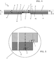
- Figure 5 shows a detail, on a larger scale, of the card, in the region of the cutting and pre-cut lines, according to a variation of embodiment in which the first pre-cut line 4 and/or the second pre-cut line 6 are formed in only a predetermined thickness C1 of the substrate 2.
- the pre-cut line 4 stops before it reaches the opposite surface SC, the rest of the supporting base not being affected by the action of the pre-cut lines, thus determining in fact the force necessary for detachment of the associated first sector 5, while the second pre-cut line 6 passes through part of the surface SC, but not the screen-printed coating 8; in this case also the rest of the support not affected by the action of the pre-cutting lines determines the force necessary for detachment.
- the cutting line 9 passes through the whole of the card, so that light may pass through it.
- Figure 6 shows a further variation of embodiment in which the pre-cut line 6 is formed entering into the support on opposite sides thereof and stops in a zone of the surface of the surface SC, without the two opposite leading ends touching; in this case also the rest of the support (indicated by ⁇ in the figure) not affected by the action of the pre-cut lines determines the force necessary for detaching the second sector with 3FF format.
- the first pre-cut line 4 is formed in an entirely equivalent manner, the rest of the support not affected by the action of the pre-cut lines being again indicated by ⁇ in the figure.
- the cutting line 9 passes instead through the whole of the card, allowing light to pass through.
- Figures 5 and 6 show in schematic form also the different dimensions of the pre-cut lines.
- the second pre-cut line 6 is longer than the first pre-cut line 4 so as to prevent, following application of a force on the substrate 2 intended to separate the sectors from the card, separation of the first sector 5 from the substrate 2 occurring before separation of the second sector 7 from the said substrate.
- the first sector 5 is separated together with the circuit 3 from the second sector 7, only after the second sector 7, comprising the first sector 5 and the circuit 3, is separated from the card 1.
- the cutting line 9 is such as to prevent, following application of a force on the substrate 2 which separates the sectors from the card, separation of the second sector 7 from the substrate 2 occurring before separation of the third sector 10 from the said substrate 2.
- the second sector 7 is separated together with the circuit 3 from the third sector 10, only after the third sector 10, comprising the second sector 7 and the circuit 3, is separated from the card 1.
- the first sector 5 may be separated together with the circuit 3 from the second sector 7, namely after the second sector 7, comprising the first sector 5 and the circuit 3, has been separated from the third sector 10.
- the method of manufacturing the card 1 comprises a preliminary step of providing a substrate 2, for example made of plastic, and integrating a circuit 3 in the substrate 2, with the pads of the circuit 3 substantially coplanar with a surface S of the substrate 2.
- the method may also comprise a step of:
- Definition of the cutting lines and pre-cut lines may be performed before or after application of the screen-printed coating.
- the screen-printing coating step is performed first and then the card is subjected to a mechanical process in order to define the cutting lines and pre-cut lines corresponding to the 2FF, 3FF and 4FF formats.
- the cutting line 9 comprises a structure with three attachment points, having calibrated dimensions at the points; the three-point structure corresponds substantially to a channel all the way around the third sector 10, except for the 3 points.
- the third sector 10 in the 2FF format is the first sector which is detached from the card 1 when a force is applied onto the substrate 2.
- the pre-cut lines 6 and 4 of the sections 7 and 5 are formed by means of the penetration into the substrate 2 of cutting edges at an angle of about 15°-25° with respect to the surface S of the substrate. Essentially, no light is able to pass through from one side to the other of the card 1, even following the formation of the pre-cut lines.
- the penetration of the cutting edges is calibrated both on the top side (surface S) and on the bottom side (surface SC) of the substrate 2 and is calibrated so as to terminate at a middle line of the substrate.
- the screen-printed coating situated on the substrate or on the outer sector i.e. that not comprising the integrated circuit
- the screen-printed coating situated on the substrate or on the outer sector is deformed, by an amount at least sufficient to prevent reuse of the frame (substrate or sector) as an adaptor.
- the screen-printed coating 8 is applied in such a way that the thickness of the first sector 5 (4FF) complies with the standard ETSI TS 102 221 V 11.0.0 and the thickness of the sectors 10 and 7 complies with the standards ETSI TS 102 221 V 11.0.0 and ISO/IEC 7810:2003. All the formats comply with the standards ISO/IEC 7816-1 and ISO/IEC 7816-2.
- the coating application step is performed by compressing the screen-printing ink on the substrate through a mesh, preferably made of fabric, and, by means of a doctor blade, applied with a predetermined pressure on the mesh.
- a mesh preferably made of fabric
- Application of the screen-printed coating fully replaces the lamination steps performed according to the prior art, thereby avoiding the complex treatment of the plastic mixtures by means of heating and cooling, and application thereof in layers, in order to define the sectors.
- the screen-printed coating prevents damage to the structure of the substrate or the pre-incisions formed therein and allows graphical processing of the card to be performed prior to structural formation of the 2FF, 3FF and, if appropriate, 4FF sectors. Moreover, it is possible to print an image also in the opposite surface of the substrate associated with the 4FF format sector.
- the card is more reliable than the known cards because application of the screen-printed coating improves the removability of the sectors, especially in the case of the 3FF and 4FF sectors which are situated very close to each other.
- a thickness of the substrate preferably towards the opposite surface, joins the sectors together or to the substrate, consolidating the structure of the card and preventing accidental separation of the sectors from the card.
Landscapes
- Engineering & Computer Science (AREA)
- Computer Hardware Design (AREA)
- Microelectronics & Electronic Packaging (AREA)
- Physics & Mathematics (AREA)
- General Physics & Mathematics (AREA)
- Theoretical Computer Science (AREA)
- Credit Cards Or The Like (AREA)
Claims (13)
- Karte mit integriertem Schaltkreis (1), die ein Substrat (2) und einen Schaltkreis (3) umfasst, der in das Substrat (2) integriert ist, wobei die Kontaktflächen des Schaltkreises (3) im Wesentlichen komplanar mit einer Oberfläche (S) des Substrats (2) sind, wobei
das Substrat (2) einen ersten Bereich umfasst, der einen ersten Sektor (5) des Substrats (2) definiert, der den Schaltkreis (3) umfasst und in der Lage ist, von der Karte (1) abgetrennt zu werden, wobei der erste Sektor (5) eine Form und eine Größe aufweist, die äquivalent zu einem 4FF-Format von Karten mit integriertem Schaltkreis sind und dafür vorgesehen sind, um von der Karte mithilfe der Bildung einer ersten vorgestanzten oder perforierten Linie (4) abgetrennt zu werden, die den ersten Sektor (5) mit dem 4FF-Format begrenzt, wobei die Karte außerdem umfasst:mindestens einen zweiten Bereich, der einen zweiten Sektor (7) um den ersten Sektor (5) definiert und in der Lage ist, aufgrund der Bildung einer zweiten vorgestanzten oder perforierten Linie (6) von der Karte (1) abgetrennt zu werden, wobei der zweite Sektor (7) eine Form und eine Größe aufweist, die äquivalent zu einem 2FF- oder 3FF-Format von Karten mit integrierten Schaltkreis sind,eine Beschichtung (8) auf der zur Oberfläche (S) entgegengesetzten Oberfläche (SC) des Substrats (2) in dem Bereich zumindest des zweiten Sektors (7),wobei die Beschichtung (8) entlang des zweiten Sektors (7) eine Dicke (B) aufweist, die gleich einer Differenz zwischen einer vordefinierten Dicke (X) des 2FF- oder des 3FF-Formats und einer Dicke (A) des ersten Sektors (5) ist,dadurch gekennzeichnet, dass die Beschichtung (8) siebgedruckt ist. - Karte mit integriertem Schaltkreis (1) nach Anspruch 1, dadurch gekennzeichnet, dass die Dicke (A) des ersten Sektors (5) gleich einer Dicke (C) des Substrats (2) und einer vordefinierten Dicke (Y) des 4FF-Formats von Karten mit integriertem Schaltkreis ist.
- Karte mit integriertem Schaltkreis (1) nach Anspruch 1, dadurch gekennzeichnet, dass die Dicke (C) des Substrats (2) kleiner als eine vordefinierte Dicke (Y) des 4FF-Formats von Karten mit integriertem Schaltkreis ist und dadurch, dass die siebgedruckte Beschichtung (8) auch die entgegengesetzte Oberfläche (SC) des Substrats (2) entlang des ersten Sektors (5) mit einer Dicke (D) abdeckt, die gleich der Differenz zwischen der vordefinierten Dicke (Y) des 4FF-Formats und der Dicke (C) des Substrats (2) ist, die den ersten Sektor (5) mit einer Dicke (A) bereitstellt, die gleich der vordefinierten Dicke (Y) für das 4FF-Format von Karten mit integriertem Schaltkreis ist.
- Karte mit integriertem Schaltkreis (1) nach Anspruch 1, dadurch gekennzeichnet, dass sie einen dritten Bereich umfasst, der einen dritten Sektor (10) um den zweiten Sektor (7) definiert, wobei der zweite Sektor (7) eine Form und eine Größe aufweist, die äquivalent zu dem 3FF-Format von Karten mit integrierten Schaltkreis sind, und wobei der dritte Sektor (10) eine Form und eine Größe aufweist, die äquivalent zu dem 2FF-Format von Karten mit integrierten Schaltkreis sind, wobei der dritte Sektor (10) vorgesehen ist, um mithilfe einer Scherstanzung von der Karte (1) abgetrennt zu werden, und wobei die siebgedruckte Beschichtung (8) mindestens entlang des zweiten Sektors (7) und des dritten Sektors (10) appliziert wird.
- Karte mit integriertem Schaltkreis (1) nach Anspruch 1, dadurch gekennzeichnet, dass das Substrat (2) eine vordefinierte Form und eine Größe aufweist, die äquivalent zu dem 1FF-Format von Karten mit integrierten Schaltkreis sind.
- Karte mit integriertem Schaltkreis (1) nach Anspruch 1, dadurch gekennzeichnet, dass die siebgedruckte Beschichtung (8) über der gesamten entgegengesetzten Oberfläche (SC) des Substrats (2) mit Ausnahme entlang des ersten Sektors (5) appliziert wird.
- Karte mit integriertem Schaltkreis (1) nach Anspruch 1, dadurch gekennzeichnet, dass die erste vorgestanzte Linie (4) und/oder die zweite vorgestanzte Linie (6) nur in dem Substrat (2) gebildet werden.
- Karte mit integriertem Schaltkreis (1) nach Anspruch 1 oder 4, dadurch gekennzeichnet, dass die erste vorgestanzte Linie (4) und/oder die zweite vorgestanzte Linie (6) nur in einer vorbestimmten Dicke (C1) des Substrats (2) gebildet werden.
- Karte mit integriertem Schaltkreis (1) nach Anspruch 1 oder 4, dadurch gekennzeichnet, dass die erste vorgestanzte Linie (4) und/oder die zweite vorgestanzte Linie (6) sowohl in einer vorbestimmten Dicke (C1) des Substrats (2) als auch in einer vorbestimmten Dicke (C2) der siebgedruckten Beschichtung gebildet werden.
- Karte mit integriertem Schaltkreis (1) nach Anspruch 1, dadurch gekennzeichnet, dass die zweite vorgestanzte Linie (6) durch eine größere Tiefe als die erste vorgestanzte Linie (4) gekennzeichnet ist.
- Karte mit integriertem Schaltkreis (1) nach Anspruch 4, dadurch gekennzeichnet, dass die Schnittlinie (9) die gesamte tragende Basis der Karte (1) durchquert.
- Verfahren zum Herstellen einer Karte mit integriertem Schaltkreis (1), das die Schritte eines Integrierens eines Schaltkreises (3) umfasst, der in ein Substrat (2) integriert ist, wobei die Kontaktflächen des Schaltkreises (3) im Wesentlichen komplanar mit einer Oberfläche (S) des Substrats (2) sind, und wobei das Verfahren die folgenden Schritte aufweist:- Definieren in dem Substrat (2) mindestens eines ersten Bereichs, der einen ersten Sektor (5) definiert, der die Form und die Größe aufweist, die äquivalent zu einem 4FF-Format sind, und mindestens eines zweiten Bereichs, der einen zweiten Sektor (7) definiert, der eine Form und eine Größe aufweist, die äquivalent zu einem 3FF- oder 2FF-Format um den ersten Sektor (5) sind, wobei diese Sektoren dafür vorgesehen sind, von der Karte (1) abgetrennt zu werden;- Applizieren einer siebgedruckten Beschichtung (8) auf der zur Oberfläche (S) entgegengesetzten Oberfläche (SC) des Substrats (2) in dem Bereich von mindestens dem zweiten Sektor (7) mit dem 3FF- oder dem 2FF-Format von Karten mit integriertem Schaltkreis, wobei die siebgedruckte Beschichtung (8) entlang des zweiten Sektors (7) so appliziert wird, dass sie eine Dicke (B) bildet, die gleich einer Differenz zwischen einer vordefinierten Dicke (X) des 2FF- oder des 3FF-Formats und einer Dicke (A) des ersten Sektors (5) mit dem 4FF-Format ist;- Bilden einer ersten vorgestanzten oder perforierten Linie (4) in dem Substrat (2), die den ersten Sektor (5) mit dem 4FF-Format des Substrats (2) begrenzt, der den Schaltkreis (3) aufweist und gestaltet ist, um von der Karte (1) abgetrennt zu werden; und- Bilden mindestens einer zweiten vorgestanzten oder perforierten Linie (6) in dem Substrat (2), die den zweiten Sektor (7) um den ersten Sektor (5) mit dem 4FF-Format begrenzt und gestaltet ist, um von der Karte (1) abgetrennt zu werden.
- Herstellungsverfahren nach Anspruch 12, dadurch gekennzeichnet, dass es außerdem einen Schritt- eines Bildens einer Schnittlinie (9) umfasst, die einen dritten Sektor (10) um den zweiten Sektor (7) begrenzt und eine Form und eine Größe aufweist, die äquivalent zu einem 2FF-Format von Karten mit integriertem Schaltkreis sind.
Applications Claiming Priority (2)
| Application Number | Priority Date | Filing Date | Title |
|---|---|---|---|
| ITMI20140584 | 2014-04-02 | ||
| PCT/IB2015/051947 WO2015150949A1 (en) | 2014-04-02 | 2015-03-17 | Enhanced ic card |
Publications (2)
| Publication Number | Publication Date |
|---|---|
| EP3127046A1 EP3127046A1 (de) | 2017-02-08 |
| EP3127046B1 true EP3127046B1 (de) | 2019-05-22 |
Family
ID=50877572
Family Applications (1)
| Application Number | Title | Priority Date | Filing Date |
|---|---|---|---|
| EP15714652.3A Active EP3127046B1 (de) | 2014-04-02 | 2015-03-17 | Verbesserte ic-karte |
Country Status (4)
| Country | Link |
|---|---|
| US (1) | US9235797B2 (de) |
| EP (1) | EP3127046B1 (de) |
| CN (1) | CN106104584B (de) |
| WO (1) | WO2015150949A1 (de) |
Families Citing this family (2)
| Publication number | Priority date | Publication date | Assignee | Title |
|---|---|---|---|---|
| WO2018005134A1 (en) * | 2016-06-29 | 2018-01-04 | Giesecke+Devrient Mobile Security America, Inc. | Automatic sim punch and method |
| DE202017006593U1 (de) * | 2017-12-22 | 2018-01-26 | Giesecke+Devrient Mobile Security Gmbh | Teilnehmer-Identifikationsmodul für ein Mobilfunknetz |
Family Cites Families (12)
| Publication number | Priority date | Publication date | Assignee | Title |
|---|---|---|---|---|
| GB2319705B (en) * | 1996-11-21 | 2001-01-24 | Motorola Ltd | Arrangement for encryption/decryption of data and data carrier incorporating same |
| US7628336B2 (en) * | 2007-05-25 | 2009-12-08 | Target Brands, Inc. | Transaction card with thermochromic feature |
| EP2288879B1 (de) * | 2008-06-04 | 2018-01-24 | G Patel | Auf metallätzung basierendes überwachungssystem |
| US20110293851A1 (en) * | 2009-02-02 | 2011-12-01 | Bollstroem Roger | Method for creating a substrate for printed or coated functionality, substrate, functional device and its use |
| FR2958208B1 (fr) * | 2010-03-30 | 2012-08-31 | Oberthur Technologies | Support comprenant un element detachable, procede de detachement d'un tel element detachable et procede de fabrication d'un tel support |
| US8573986B2 (en) * | 2010-07-30 | 2013-11-05 | Sharpe Innovations, Inc. | SIM card adaptor |
| FR2982981B1 (fr) * | 2011-11-22 | 2016-07-01 | Oberthur Technologies | Adaptateur pour carte a microcircuit entre un grand format et un petit format de moindre epaisseur |
| EP2605188A1 (de) * | 2011-12-14 | 2013-06-19 | Gemalto SA | Verfahren zur Herstellung von Chip-Karten |
| FR2985345B1 (fr) * | 2011-12-29 | 2021-11-26 | Oberthur Technologies | Procede de fabrication d'une carte de petite epaisseur detachable d'une plaque de grande epaisseur |
| DE102012001776A1 (de) * | 2012-01-31 | 2013-08-01 | Giesecke & Devrient Gmbh | Chipkarte mit heraustrennbarer Miniaturchipkarte |
| CN104159328A (zh) * | 2013-05-14 | 2014-11-19 | 索尼公司 | 识别卡信息的提示方法、移动终端以及电子设备 |
| CN103400178A (zh) * | 2013-07-31 | 2013-11-20 | 北京大拙至诚科技发展有限公司 | 具有多种规格的小卡的卡基 |
-
2015
- 2015-03-17 EP EP15714652.3A patent/EP3127046B1/de active Active
- 2015-03-17 WO PCT/IB2015/051947 patent/WO2015150949A1/en not_active Ceased
- 2015-03-17 CN CN201580012123.XA patent/CN106104584B/zh active Active
- 2015-03-23 US US14/665,323 patent/US9235797B2/en active Active
Non-Patent Citations (1)
| Title |
|---|
| None * |
Also Published As
| Publication number | Publication date |
|---|---|
| EP3127046A1 (de) | 2017-02-08 |
| CN106104584B (zh) | 2019-02-19 |
| US20150286920A1 (en) | 2015-10-08 |
| US9235797B2 (en) | 2016-01-12 |
| CN106104584A (zh) | 2016-11-09 |
| WO2015150949A1 (en) | 2015-10-08 |
Similar Documents
| Publication | Publication Date | Title |
|---|---|---|
| CN111937007B (zh) | 具有金属框架的便携式双接口数据载体 | |
| US9195930B2 (en) | Method for manufacturing a card based on a substrate | |
| JP4853733B2 (ja) | 組み合わされたuiccプラグインアダプタを備えたミニuiccチップカード媒体の製造方法と得られた媒体 | |
| US10040308B2 (en) | Card incorporating a visible valuable object | |
| JP2008541253A (ja) | メモリデバイスのための接着フォーマットアダプタと製造方法 | |
| US9235797B2 (en) | Enhanced IC card | |
| US6575375B1 (en) | Portable integrated circuit device and method for the production thereof | |
| CN104995643B (zh) | 用于制造嵌入件的方法以及用于针对价值文件或可靠文件的膜复合件的嵌入件 | |
| CN101609514A (zh) | 一种高效电子标签制作方法 | |
| US9305254B2 (en) | Method of manufacturing a card of small thickness detachable from a plate of large thickness | |
| US9616616B2 (en) | Method for laminating a component by means of a laminating tool with a laminating element | |
| US20160368161A1 (en) | Tooling and a method for weakening an outline in a thin plastics card | |
| US10207420B2 (en) | Fabricating a plate of large thickness including a detachable card of small thickness | |
| EP2774086B1 (de) | Vorgestanzte chipkarte | |
| US9406014B2 (en) | Top gated method for manufacturing a data carrier | |
| CN111566671B (zh) | Sim卡的制造方法及sim卡 | |
| JP2014532912A5 (de) | ||
| EP2851849B1 (de) | Kartenkörper, Herstellungsverfahren für eine IC-Karte und die IC-Karte | |
| CN101116091B (zh) | 集成有sim模块的芯片卡及其冲压模 | |
| US20170270397A1 (en) | Data Carrier Comprising a Partial Piece | |
| KR102928816B1 (ko) | 패턴 형성 시 불량을 개선한 메탈카드 제조방법 | |
| WO2016091834A1 (en) | Method and device for manufacturing smart cards and a smart card made using the method | |
| US9430731B2 (en) | IC card | |
| EP2674897A1 (de) | Datenträger mit einer Chipkarte und entsprechendes Herstellungsverfahren | |
| WO2015040027A1 (en) | Method and device for manufacturing a chip card, and chip card obtained by said method |
Legal Events
| Date | Code | Title | Description |
|---|---|---|---|
| STAA | Information on the status of an ep patent application or granted ep patent |
Free format text: STATUS: THE INTERNATIONAL PUBLICATION HAS BEEN MADE |
|
| PUAI | Public reference made under article 153(3) epc to a published international application that has entered the european phase |
Free format text: ORIGINAL CODE: 0009012 |
|
| STAA | Information on the status of an ep patent application or granted ep patent |
Free format text: STATUS: REQUEST FOR EXAMINATION WAS MADE |
|
| 17P | Request for examination filed |
Effective date: 20160808 |
|
| AK | Designated contracting states |
Kind code of ref document: A1 Designated state(s): AL AT BE BG CH CY CZ DE DK EE ES FI FR GB GR HR HU IE IS IT LI LT LU LV MC MK MT NL NO PL PT RO RS SE SI SK SM TR |
|
| AX | Request for extension of the european patent |
Extension state: BA ME |
|
| DAV | Request for validation of the european patent (deleted) | ||
| DAX | Request for extension of the european patent (deleted) | ||
| GRAP | Despatch of communication of intention to grant a patent |
Free format text: ORIGINAL CODE: EPIDOSNIGR1 |
|
| STAA | Information on the status of an ep patent application or granted ep patent |
Free format text: STATUS: GRANT OF PATENT IS INTENDED |
|
| INTG | Intention to grant announced |
Effective date: 20181221 |
|
| GRAS | Grant fee paid |
Free format text: ORIGINAL CODE: EPIDOSNIGR3 |
|
| GRAA | (expected) grant |
Free format text: ORIGINAL CODE: 0009210 |
|
| STAA | Information on the status of an ep patent application or granted ep patent |
Free format text: STATUS: THE PATENT HAS BEEN GRANTED |
|
| AK | Designated contracting states |
Kind code of ref document: B1 Designated state(s): AL AT BE BG CH CY CZ DE DK EE ES FI FR GB GR HR HU IE IS IT LI LT LU LV MC MK MT NL NO PL PT RO RS SE SI SK SM TR |
|
| REG | Reference to a national code |
Ref country code: GB Ref legal event code: FG4D |
|
| REG | Reference to a national code |
Ref country code: CH Ref legal event code: EP |
|
| REG | Reference to a national code |
Ref country code: IE Ref legal event code: FG4D |
|
| REG | Reference to a national code |
Ref country code: AT Ref legal event code: REF Ref document number: 1136991 Country of ref document: AT Kind code of ref document: T Effective date: 20190615 |
|
| REG | Reference to a national code |
Ref country code: DE Ref legal event code: R096 Ref document number: 602015030739 Country of ref document: DE |
|
| REG | Reference to a national code |
Ref country code: NL Ref legal event code: MP Effective date: 20190522 |
|
| REG | Reference to a national code |
Ref country code: LT Ref legal event code: MG4D |
|
| PG25 | Lapsed in a contracting state [announced via postgrant information from national office to epo] |
Ref country code: FI Free format text: LAPSE BECAUSE OF FAILURE TO SUBMIT A TRANSLATION OF THE DESCRIPTION OR TO PAY THE FEE WITHIN THE PRESCRIBED TIME-LIMIT Effective date: 20190522 Ref country code: SE Free format text: LAPSE BECAUSE OF FAILURE TO SUBMIT A TRANSLATION OF THE DESCRIPTION OR TO PAY THE FEE WITHIN THE PRESCRIBED TIME-LIMIT Effective date: 20190522 Ref country code: ES Free format text: LAPSE BECAUSE OF FAILURE TO SUBMIT A TRANSLATION OF THE DESCRIPTION OR TO PAY THE FEE WITHIN THE PRESCRIBED TIME-LIMIT Effective date: 20190522 Ref country code: LT Free format text: LAPSE BECAUSE OF FAILURE TO SUBMIT A TRANSLATION OF THE DESCRIPTION OR TO PAY THE FEE WITHIN THE PRESCRIBED TIME-LIMIT Effective date: 20190522 Ref country code: NL Free format text: LAPSE BECAUSE OF FAILURE TO SUBMIT A TRANSLATION OF THE DESCRIPTION OR TO PAY THE FEE WITHIN THE PRESCRIBED TIME-LIMIT Effective date: 20190522 Ref country code: AL Free format text: LAPSE BECAUSE OF FAILURE TO SUBMIT A TRANSLATION OF THE DESCRIPTION OR TO PAY THE FEE WITHIN THE PRESCRIBED TIME-LIMIT Effective date: 20190522 Ref country code: PT Free format text: LAPSE BECAUSE OF FAILURE TO SUBMIT A TRANSLATION OF THE DESCRIPTION OR TO PAY THE FEE WITHIN THE PRESCRIBED TIME-LIMIT Effective date: 20190922 Ref country code: NO Free format text: LAPSE BECAUSE OF FAILURE TO SUBMIT A TRANSLATION OF THE DESCRIPTION OR TO PAY THE FEE WITHIN THE PRESCRIBED TIME-LIMIT Effective date: 20190822 Ref country code: HR Free format text: LAPSE BECAUSE OF FAILURE TO SUBMIT A TRANSLATION OF THE DESCRIPTION OR TO PAY THE FEE WITHIN THE PRESCRIBED TIME-LIMIT Effective date: 20190522 |
|
| PG25 | Lapsed in a contracting state [announced via postgrant information from national office to epo] |
Ref country code: GR Free format text: LAPSE BECAUSE OF FAILURE TO SUBMIT A TRANSLATION OF THE DESCRIPTION OR TO PAY THE FEE WITHIN THE PRESCRIBED TIME-LIMIT Effective date: 20190823 Ref country code: RS Free format text: LAPSE BECAUSE OF FAILURE TO SUBMIT A TRANSLATION OF THE DESCRIPTION OR TO PAY THE FEE WITHIN THE PRESCRIBED TIME-LIMIT Effective date: 20190522 Ref country code: LV Free format text: LAPSE BECAUSE OF FAILURE TO SUBMIT A TRANSLATION OF THE DESCRIPTION OR TO PAY THE FEE WITHIN THE PRESCRIBED TIME-LIMIT Effective date: 20190522 Ref country code: BG Free format text: LAPSE BECAUSE OF FAILURE TO SUBMIT A TRANSLATION OF THE DESCRIPTION OR TO PAY THE FEE WITHIN THE PRESCRIBED TIME-LIMIT Effective date: 20190822 |
|
| REG | Reference to a national code |
Ref country code: AT Ref legal event code: MK05 Ref document number: 1136991 Country of ref document: AT Kind code of ref document: T Effective date: 20190522 |
|
| PG25 | Lapsed in a contracting state [announced via postgrant information from national office to epo] |
Ref country code: CZ Free format text: LAPSE BECAUSE OF FAILURE TO SUBMIT A TRANSLATION OF THE DESCRIPTION OR TO PAY THE FEE WITHIN THE PRESCRIBED TIME-LIMIT Effective date: 20190522 Ref country code: RO Free format text: LAPSE BECAUSE OF FAILURE TO SUBMIT A TRANSLATION OF THE DESCRIPTION OR TO PAY THE FEE WITHIN THE PRESCRIBED TIME-LIMIT Effective date: 20190522 Ref country code: DK Free format text: LAPSE BECAUSE OF FAILURE TO SUBMIT A TRANSLATION OF THE DESCRIPTION OR TO PAY THE FEE WITHIN THE PRESCRIBED TIME-LIMIT Effective date: 20190522 Ref country code: AT Free format text: LAPSE BECAUSE OF FAILURE TO SUBMIT A TRANSLATION OF THE DESCRIPTION OR TO PAY THE FEE WITHIN THE PRESCRIBED TIME-LIMIT Effective date: 20190522 Ref country code: EE Free format text: LAPSE BECAUSE OF FAILURE TO SUBMIT A TRANSLATION OF THE DESCRIPTION OR TO PAY THE FEE WITHIN THE PRESCRIBED TIME-LIMIT Effective date: 20190522 Ref country code: SK Free format text: LAPSE BECAUSE OF FAILURE TO SUBMIT A TRANSLATION OF THE DESCRIPTION OR TO PAY THE FEE WITHIN THE PRESCRIBED TIME-LIMIT Effective date: 20190522 |
|
| REG | Reference to a national code |
Ref country code: DE Ref legal event code: R097 Ref document number: 602015030739 Country of ref document: DE |
|
| PG25 | Lapsed in a contracting state [announced via postgrant information from national office to epo] |
Ref country code: SM Free format text: LAPSE BECAUSE OF FAILURE TO SUBMIT A TRANSLATION OF THE DESCRIPTION OR TO PAY THE FEE WITHIN THE PRESCRIBED TIME-LIMIT Effective date: 20190522 |
|
| PLBE | No opposition filed within time limit |
Free format text: ORIGINAL CODE: 0009261 |
|
| STAA | Information on the status of an ep patent application or granted ep patent |
Free format text: STATUS: NO OPPOSITION FILED WITHIN TIME LIMIT |
|
| PG25 | Lapsed in a contracting state [announced via postgrant information from national office to epo] |
Ref country code: TR Free format text: LAPSE BECAUSE OF FAILURE TO SUBMIT A TRANSLATION OF THE DESCRIPTION OR TO PAY THE FEE WITHIN THE PRESCRIBED TIME-LIMIT Effective date: 20190522 |
|
| 26N | No opposition filed |
Effective date: 20200225 |
|
| PG25 | Lapsed in a contracting state [announced via postgrant information from national office to epo] |
Ref country code: PL Free format text: LAPSE BECAUSE OF FAILURE TO SUBMIT A TRANSLATION OF THE DESCRIPTION OR TO PAY THE FEE WITHIN THE PRESCRIBED TIME-LIMIT Effective date: 20190522 |
|
| PG25 | Lapsed in a contracting state [announced via postgrant information from national office to epo] |
Ref country code: SI Free format text: LAPSE BECAUSE OF FAILURE TO SUBMIT A TRANSLATION OF THE DESCRIPTION OR TO PAY THE FEE WITHIN THE PRESCRIBED TIME-LIMIT Effective date: 20190522 |
|
| PGFP | Annual fee paid to national office [announced via postgrant information from national office to epo] |
Ref country code: FR Payment date: 20200220 Year of fee payment: 6 |
|
| PG25 | Lapsed in a contracting state [announced via postgrant information from national office to epo] |
Ref country code: MC Free format text: LAPSE BECAUSE OF FAILURE TO SUBMIT A TRANSLATION OF THE DESCRIPTION OR TO PAY THE FEE WITHIN THE PRESCRIBED TIME-LIMIT Effective date: 20190522 |
|
| REG | Reference to a national code |
Ref country code: CH Ref legal event code: PL |
|
| REG | Reference to a national code |
Ref country code: BE Ref legal event code: MM Effective date: 20200331 |
|
| PG25 | Lapsed in a contracting state [announced via postgrant information from national office to epo] |
Ref country code: LU Free format text: LAPSE BECAUSE OF NON-PAYMENT OF DUE FEES Effective date: 20200317 |
|
| PG25 | Lapsed in a contracting state [announced via postgrant information from national office to epo] |
Ref country code: IE Free format text: LAPSE BECAUSE OF NON-PAYMENT OF DUE FEES Effective date: 20200317 Ref country code: LI Free format text: LAPSE BECAUSE OF NON-PAYMENT OF DUE FEES Effective date: 20200331 Ref country code: CH Free format text: LAPSE BECAUSE OF NON-PAYMENT OF DUE FEES Effective date: 20200331 |
|
| PG25 | Lapsed in a contracting state [announced via postgrant information from national office to epo] |
Ref country code: BE Free format text: LAPSE BECAUSE OF NON-PAYMENT OF DUE FEES Effective date: 20200331 |
|
| GBPC | Gb: european patent ceased through non-payment of renewal fee |
Effective date: 20200317 |
|
| PG25 | Lapsed in a contracting state [announced via postgrant information from national office to epo] |
Ref country code: GB Free format text: LAPSE BECAUSE OF NON-PAYMENT OF DUE FEES Effective date: 20200317 |
|
| PG25 | Lapsed in a contracting state [announced via postgrant information from national office to epo] |
Ref country code: FR Free format text: LAPSE BECAUSE OF NON-PAYMENT OF DUE FEES Effective date: 20210331 |
|
| PG25 | Lapsed in a contracting state [announced via postgrant information from national office to epo] |
Ref country code: MT Free format text: LAPSE BECAUSE OF FAILURE TO SUBMIT A TRANSLATION OF THE DESCRIPTION OR TO PAY THE FEE WITHIN THE PRESCRIBED TIME-LIMIT Effective date: 20190522 Ref country code: CY Free format text: LAPSE BECAUSE OF FAILURE TO SUBMIT A TRANSLATION OF THE DESCRIPTION OR TO PAY THE FEE WITHIN THE PRESCRIBED TIME-LIMIT Effective date: 20190522 |
|
| PG25 | Lapsed in a contracting state [announced via postgrant information from national office to epo] |
Ref country code: MK Free format text: LAPSE BECAUSE OF FAILURE TO SUBMIT A TRANSLATION OF THE DESCRIPTION OR TO PAY THE FEE WITHIN THE PRESCRIBED TIME-LIMIT Effective date: 20190522 Ref country code: IS Free format text: LAPSE BECAUSE OF FAILURE TO SUBMIT A TRANSLATION OF THE DESCRIPTION OR TO PAY THE FEE WITHIN THE PRESCRIBED TIME-LIMIT Effective date: 20190922 |
|
| REG | Reference to a national code |
Ref country code: DE Ref legal event code: R081 Ref document number: 602015030739 Country of ref document: DE Owner name: STMICROELECTRONICS INTERNATIONAL N.V., PLAN-LE, CH Free format text: FORMER OWNER: STMICROELECTRONICS S.R.L., AGRATE BRIANZA, IT |
|
| PGFP | Annual fee paid to national office [announced via postgrant information from national office to epo] |
Ref country code: IT Payment date: 20250218 Year of fee payment: 11 |
|
| PGFP | Annual fee paid to national office [announced via postgrant information from national office to epo] |
Ref country code: DE Payment date: 20260219 Year of fee payment: 12 |