EP3124921B1 - Position measuring device - Google Patents
Position measuring device Download PDFInfo
- Publication number
- EP3124921B1 EP3124921B1 EP15179014.4A EP15179014A EP3124921B1 EP 3124921 B1 EP3124921 B1 EP 3124921B1 EP 15179014 A EP15179014 A EP 15179014A EP 3124921 B1 EP3124921 B1 EP 3124921B1
- Authority
- EP
- European Patent Office
- Prior art keywords
- sensor unit
- unit
- graduation
- scanning
- measurement device
- Prior art date
- Legal status (The legal status is an assumption and is not a legal conclusion. Google has not performed a legal analysis and makes no representation as to the accuracy of the status listed.)
- Active
Links
- 238000005259 measurement Methods 0.000 claims description 31
- 239000000463 material Substances 0.000 claims description 26
- 239000004065 semiconductor Substances 0.000 claims description 19
- 230000001681 protective effect Effects 0.000 claims description 15
- 230000003287 optical effect Effects 0.000 claims description 11
- 238000005286 illumination Methods 0.000 claims description 9
- 238000004382 potting Methods 0.000 claims description 7
- 238000004026 adhesive bonding Methods 0.000 claims description 2
- 239000011796 hollow space material Substances 0.000 claims 1
- 239000002966 varnish Substances 0.000 claims 1
- 239000007788 liquid Substances 0.000 description 13
- 238000005070 sampling Methods 0.000 description 9
- 238000000034 method Methods 0.000 description 8
- 238000004519 manufacturing process Methods 0.000 description 7
- 230000008569 process Effects 0.000 description 6
- 238000012545 processing Methods 0.000 description 6
- 150000001875 compounds Chemical class 0.000 description 5
- 229910052751 metal Inorganic materials 0.000 description 5
- 239000002184 metal Substances 0.000 description 5
- 239000002245 particle Substances 0.000 description 5
- 229910052710 silicon Inorganic materials 0.000 description 5
- 239000010703 silicon Substances 0.000 description 5
- XUIMIQQOPSSXEZ-UHFFFAOYSA-N Silicon Chemical compound [Si] XUIMIQQOPSSXEZ-UHFFFAOYSA-N 0.000 description 4
- 230000000694 effects Effects 0.000 description 4
- 238000005516 engineering process Methods 0.000 description 4
- 238000005476 soldering Methods 0.000 description 4
- 238000010276 construction Methods 0.000 description 3
- 238000011109 contamination Methods 0.000 description 3
- 230000001419 dependent effect Effects 0.000 description 3
- 230000008901 benefit Effects 0.000 description 2
- 238000013461 design Methods 0.000 description 2
- 238000011161 development Methods 0.000 description 2
- 239000011521 glass Substances 0.000 description 2
- 239000004033 plastic Substances 0.000 description 2
- 230000035945 sensitivity Effects 0.000 description 2
- 229910000679 solder Inorganic materials 0.000 description 2
- 239000000758 substrate Substances 0.000 description 2
- 239000012780 transparent material Substances 0.000 description 2
- VAHKBZSAUKPEOV-UHFFFAOYSA-N 1,4-dichloro-2-(4-chlorophenyl)benzene Chemical compound C1=CC(Cl)=CC=C1C1=CC(Cl)=CC=C1Cl VAHKBZSAUKPEOV-UHFFFAOYSA-N 0.000 description 1
- VYZAMTAEIAYCRO-UHFFFAOYSA-N Chromium Chemical compound [Cr] VYZAMTAEIAYCRO-UHFFFAOYSA-N 0.000 description 1
- 239000004593 Epoxy Substances 0.000 description 1
- 238000009825 accumulation Methods 0.000 description 1
- 230000002411 adverse Effects 0.000 description 1
- PNEYBMLMFCGWSK-UHFFFAOYSA-N aluminium oxide Inorganic materials [O-2].[O-2].[O-2].[Al+3].[Al+3] PNEYBMLMFCGWSK-UHFFFAOYSA-N 0.000 description 1
- 239000011324 bead Substances 0.000 description 1
- 230000015572 biosynthetic process Effects 0.000 description 1
- 238000005266 casting Methods 0.000 description 1
- 229910010293 ceramic material Inorganic materials 0.000 description 1
- 230000008859 change Effects 0.000 description 1
- 229910052804 chromium Inorganic materials 0.000 description 1
- 239000011651 chromium Substances 0.000 description 1
- 238000004891 communication Methods 0.000 description 1
- 230000001010 compromised effect Effects 0.000 description 1
- -1 condensate Substances 0.000 description 1
- 239000004020 conductor Substances 0.000 description 1
- 239000002826 coolant Substances 0.000 description 1
- 238000012937 correction Methods 0.000 description 1
- 238000005260 corrosion Methods 0.000 description 1
- 230000007797 corrosion Effects 0.000 description 1
- 230000008030 elimination Effects 0.000 description 1
- 238000003379 elimination reaction Methods 0.000 description 1
- 239000003822 epoxy resin Substances 0.000 description 1
- 238000005530 etching Methods 0.000 description 1
- 238000011156 evaluation Methods 0.000 description 1
- 239000003365 glass fiber Substances 0.000 description 1
- 230000006872 improvement Effects 0.000 description 1
- 238000009434 installation Methods 0.000 description 1
- 239000004922 lacquer Substances 0.000 description 1
- 239000000314 lubricant Substances 0.000 description 1
- 238000013507 mapping Methods 0.000 description 1
- 229920000647 polyepoxide Polymers 0.000 description 1
- 230000005855 radiation Effects 0.000 description 1
- 230000009467 reduction Effects 0.000 description 1
- 239000007787 solid Substances 0.000 description 1
- 238000009331 sowing Methods 0.000 description 1
Images


Classifications
-
- G—PHYSICS
- G01—MEASURING; TESTING
- G01D—MEASURING NOT SPECIALLY ADAPTED FOR A SPECIFIC VARIABLE; ARRANGEMENTS FOR MEASURING TWO OR MORE VARIABLES NOT COVERED IN A SINGLE OTHER SUBCLASS; TARIFF METERING APPARATUS; MEASURING OR TESTING NOT OTHERWISE PROVIDED FOR
- G01D5/00—Mechanical means for transferring the output of a sensing member; Means for converting the output of a sensing member to another variable where the form or nature of the sensing member does not constrain the means for converting; Transducers not specially adapted for a specific variable
- G01D5/26—Mechanical means for transferring the output of a sensing member; Means for converting the output of a sensing member to another variable where the form or nature of the sensing member does not constrain the means for converting; Transducers not specially adapted for a specific variable characterised by optical transfer means, i.e. using infrared, visible, or ultraviolet light
- G01D5/32—Mechanical means for transferring the output of a sensing member; Means for converting the output of a sensing member to another variable where the form or nature of the sensing member does not constrain the means for converting; Transducers not specially adapted for a specific variable characterised by optical transfer means, i.e. using infrared, visible, or ultraviolet light with attenuation or whole or partial obturation of beams of light
- G01D5/34—Mechanical means for transferring the output of a sensing member; Means for converting the output of a sensing member to another variable where the form or nature of the sensing member does not constrain the means for converting; Transducers not specially adapted for a specific variable characterised by optical transfer means, i.e. using infrared, visible, or ultraviolet light with attenuation or whole or partial obturation of beams of light the beams of light being detected by photocells
- G01D5/347—Mechanical means for transferring the output of a sensing member; Means for converting the output of a sensing member to another variable where the form or nature of the sensing member does not constrain the means for converting; Transducers not specially adapted for a specific variable characterised by optical transfer means, i.e. using infrared, visible, or ultraviolet light with attenuation or whole or partial obturation of beams of light the beams of light being detected by photocells using displacement encoding scales
- G01D5/34707—Scales; Discs, e.g. fixation, fabrication, compensation
- G01D5/34715—Scale reading or illumination devices
-
- H—ELECTRICITY
- H01—ELECTRIC ELEMENTS
- H01L—SEMICONDUCTOR DEVICES NOT COVERED BY CLASS H10
- H01L31/00—Semiconductor devices sensitive to infrared radiation, light, electromagnetic radiation of shorter wavelength or corpuscular radiation and specially adapted either for the conversion of the energy of such radiation into electrical energy or for the control of electrical energy by such radiation; Processes or apparatus specially adapted for the manufacture or treatment thereof or of parts thereof; Details thereof
- H01L31/02—Details
- H01L31/0203—Containers; Encapsulations, e.g. encapsulation of photodiodes
-
- H—ELECTRICITY
- H02—GENERATION; CONVERSION OR DISTRIBUTION OF ELECTRIC POWER
- H02S—GENERATION OF ELECTRIC POWER BY CONVERSION OF INFRARED RADIATION, VISIBLE LIGHT OR ULTRAVIOLET LIGHT, e.g. USING PHOTOVOLTAIC [PV] MODULES
- H02S40/00—Components or accessories in combination with PV modules, not provided for in groups H02S10/00 - H02S30/00
- H02S40/40—Thermal components
- H02S40/44—Means to utilise heat energy, e.g. hybrid systems producing warm water and electricity at the same time
-
- H—ELECTRICITY
- H01—ELECTRIC ELEMENTS
- H01L—SEMICONDUCTOR DEVICES NOT COVERED BY CLASS H10
- H01L2224/00—Indexing scheme for arrangements for connecting or disconnecting semiconductor or solid-state bodies and methods related thereto as covered by H01L24/00
- H01L2224/73—Means for bonding being of different types provided for in two or more of groups H01L2224/10, H01L2224/18, H01L2224/26, H01L2224/34, H01L2224/42, H01L2224/50, H01L2224/63, H01L2224/71
- H01L2224/732—Location after the connecting process
- H01L2224/73201—Location after the connecting process on the same surface
- H01L2224/73203—Bump and layer connectors
- H01L2224/73204—Bump and layer connectors the bump connector being embedded into the layer connector
-
- H—ELECTRICITY
- H01—ELECTRIC ELEMENTS
- H01L—SEMICONDUCTOR DEVICES NOT COVERED BY CLASS H10
- H01L2224/00—Indexing scheme for arrangements for connecting or disconnecting semiconductor or solid-state bodies and methods related thereto as covered by H01L24/00
- H01L2224/73—Means for bonding being of different types provided for in two or more of groups H01L2224/10, H01L2224/18, H01L2224/26, H01L2224/34, H01L2224/42, H01L2224/50, H01L2224/63, H01L2224/71
- H01L2224/732—Location after the connecting process
- H01L2224/73251—Location after the connecting process on different surfaces
- H01L2224/73253—Bump and layer connectors
-
- Y—GENERAL TAGGING OF NEW TECHNOLOGICAL DEVELOPMENTS; GENERAL TAGGING OF CROSS-SECTIONAL TECHNOLOGIES SPANNING OVER SEVERAL SECTIONS OF THE IPC; TECHNICAL SUBJECTS COVERED BY FORMER USPC CROSS-REFERENCE ART COLLECTIONS [XRACs] AND DIGESTS
- Y02—TECHNOLOGIES OR APPLICATIONS FOR MITIGATION OR ADAPTATION AGAINST CLIMATE CHANGE
- Y02E—REDUCTION OF GREENHOUSE GAS [GHG] EMISSIONS, RELATED TO ENERGY GENERATION, TRANSMISSION OR DISTRIBUTION
- Y02E10/00—Energy generation through renewable energy sources
- Y02E10/50—Photovoltaic [PV] energy
-
- Y—GENERAL TAGGING OF NEW TECHNOLOGICAL DEVELOPMENTS; GENERAL TAGGING OF CROSS-SECTIONAL TECHNOLOGIES SPANNING OVER SEVERAL SECTIONS OF THE IPC; TECHNICAL SUBJECTS COVERED BY FORMER USPC CROSS-REFERENCE ART COLLECTIONS [XRACs] AND DIGESTS
- Y02—TECHNOLOGIES OR APPLICATIONS FOR MITIGATION OR ADAPTATION AGAINST CLIMATE CHANGE
- Y02E—REDUCTION OF GREENHOUSE GAS [GHG] EMISSIONS, RELATED TO ENERGY GENERATION, TRANSMISSION OR DISTRIBUTION
- Y02E10/00—Energy generation through renewable energy sources
- Y02E10/60—Thermal-PV hybrids
Definitions
- the present invention relates to a position measuring device according to the preamble of claim 1.
- Such position measuring devices are mainly used in automation technology for measuring paths and / or angles.
- Position measuring devices are widely used, in particular, in machine tools and in automation technology. They serve to determine the relative position of two mutually movable objects.
- length and angle encoders serve, for example, for determining the relative position of two mutually movable machine parts of a machine tool.
- a material measure for example in the form of a straight scale, on which a measurement graduation is arranged, connected to the one and a scanning unit with the other of the two objects, so that by scanning the Messannon position-dependent scanning signals are obtained, with the help of which the extent of movement of the two objects to each other in the direction of movement can be determined.
- Angle encoders also known as encoders, are based on the same principle. Instead of the scale, however, a circular disc appears here as the measuring standard, on which the measuring graduation is arranged concentrically to the point of rotation. The disc is rotatably connected to a shaft to be measured, while the scanning unit is fixedly mounted for this purpose.
- the measurement graduation may comprise one or more graduation tracks, distinguishing incremental and absolutely coded graduation tracks.
- Incremental graduation tracks consist of regularly arranged graduation elements, the scanning of which results in a uniform relative movement between the measuring standard and the scanning unit resulting in substantially sinusoidal scanning signals.
- the path determination is based on the count of the signal periods or fractions of signal periods.
- a reference point must be determined, for this purpose, for example, a reference mark is provided, which is also detected by the scanning unit.
- the absolute position can be determined directly from the scanning signals of absolutely coded graduation tracks, since these are coded in a plurality of juxtaposed graduation tracks in parallel (eg gray code, BCD code,...) Or in a graduation track serially (eg chain code, PRC) is.
- measuring graduations are also known which comprise both incremental and absolute graduation tracks.
- a widely used functional principle in position-measuring devices is optical scanning.
- the measurement graduation which is applied to a material measure, is imaged onto a number of photodetectors using directed light which is emitted by a light source.
- the material measure is movably arranged in the beam path of the light and modulates the light when the measurement graduation relative to the light source and the photodetectors is moved.
- the position or position change is determined by evaluating the output signals of the photodetectors.
- the measurement graduation may consist of areas with different optical properties, such as transparent / opaque.
- the photodetectors required for scanning are usually arranged together on a semiconductor chip, which is mounted directly on a printed circuit board by means of chip-on-board (COB) technology.
- COB chip-on-board
- the chip is first glued with its back to the circuit board and then the contact surfaces on its upper side connected by wire bonding to the circuit board.
- at least parts of the evaluation electronics for the scanning signals are arranged on the semiconductor chip in addition to the photodetectors.
- FIG. 3 schematically shows the components relevant to the position measurement of a known from the prior art position measuring device, namely a scanning unit 10 and a measuring scale 40, on which a measuring graduation 41 is arranged.
- the scanning unit 10 and the measuring scale 40 are arranged to be movable relative to each other in a measuring direction X.
- the position-measuring device is, for example, a device for length measurement (linear position-measuring device)
- the material measure 40 is designed as a straight scale, which is fastened to a first machine part and on which a measuring graduation 41 is arranged in the measuring direction X.
- the scanning unit 10 is then attached to a second machine part in such a way that during a movement of the first machine part relative to the second machine part in the measuring direction X, the scanning unit 10 is moved along the scale and thereby scans the measuring graduation 41.
- the sampling results in scanning signals from which position values are generated in further processing.
- the material measure 40 is, for example, one circular disc which is non-rotatably connected to a shaft whose angular position is to be measured.
- the measuring graduation 41 is arranged concentrically to the pivot point of the shaft.
- the scanning unit is fixed in a stationary manner in such a way that, upon rotation of the shaft to be measured, the measuring graduation can be scanned and in turn position values, in this case angle values, can be generated from the scanning signals.
- the scanning unit 10 comprises a lighting unit 20 and a detector unit 530.
- the operating principle on which the position-measuring device is based is that of the transmitted-light optical scanning.
- the illumination unit 20 emits light in the direction of the measuring graduation 41. This comprises translucent (transparent) and opaque areas which modulate the light of the illumination unit 20.
- the modulated light is imaged onto the detector unit 530 which generates position signals therefrom.
- the illumination unit 20 may include, for example, a light source 21 emitting divergent light which is collimated by a collimator 22.
- the material measure 40 is advantageously made of a transparent material, such as glass.
- the measuring graduation 41 is formed in this case by opaque areas, for example by metal, which is applied to the material measure. Particularly suitable for this purpose is, for example, chromium. But there are also conferencever stresses 40 known, which consist of an opaque material, such as a metal.
- the measuring graduation 41 can be designed as a sequence of metal webs and openings in the material measure 40.
- the detector unit 530 comprises a printed circuit board 531, a sensor unit 532 and, in particular for small graduation periods of the graduation 41 to be scanned, a scanning plate 533.
- the circuit board 531 functions inter alia as a support for the sensor unit 532, which forms the central component of the detector unit 530.
- On the circuit board 531 for example, input / output interfaces in the form of connectors etc. are arranged in addition to supporting electronic circuits for the sensor unit 532.
- the sensor unit 532 is designed as a semiconductor chip. It has a front side and a rear side, wherein the side facing the printed circuit board 531 is the rear side and the side facing the measuring graduation 41 is the front side of the sensor unit 532.
- a number of photodetectors 535 Arranged on the front side of the sensor unit 532 is a number of photodetectors 535, which serve to generate position signals by detecting the light of the illumination unit 20 modulated by the measuring graduation 41 and possibly the scanning plate 533.
- the front side of the sensor unit 532 is preferably aligned parallel to the plane in which the measuring graduation 41 is located.
- the sensor unit 532 advantageously includes additional components for processing the position signals, possibly up to the formation of position values from the position signals.
- the sensor unit may comprise a plurality of other circuit blocks, such as e.g. Error correction, circuits to ensure reliability, as well as a digital interface for communication with a subsequent electronics.
- a semiconductor chip comprising both photodetectors and signal processing components is referred to as an opto-ASIC.
- the rear side of the sensor unit 532 is connected to the circuit board 531, the connection being made for example by gluing.
- the connection being made for example by gluing.
- the circuit components of the sensor unit 532 with the printed circuit board 531 are on the front of the sensor unit 532 and on the sensor unit 532 side facing the circuit board 531st respectively corresponding contact surfaces (not shown), which are connected in a known manner by wire bonding via bonding wires 537 together.
- the bonding wires 537 are protected by a potting compound 538 from mechanical influences.
- Wire bonding is a complex manufacturing process, both in terms of the cost of the required production equipment (wire bonder), as well as the additional time required for wire bonding, the casting of the bonding wires and the curing of the potting compound.
- a dam around the photodetectors which stands for a height c relative to the front of the sensor unit 532 (ie the surface of the semiconductor chip on which the photodetectors are located) lifts.
- the height c is at least 0.5 mm in conventional manufacturing processes.
- a sampling distance d defined by the distance of the front side of the sensor unit 32 (the surface of the semiconductor chip on which the photodetectors are located) to the surface of the material measure 40 (in the example shown equate to the surface of the measuring graduation 41), between 0.55 mm and 0.7 mm are maintained in order to ensure safe operation can.
- the scanning plate 533 is particularly necessary in the scanning of small pitch periods. It is arranged between the photodetectors 535 on the front side of the sensor unit 532 and the measuring graduation 41. It has, similar to the material measure 40, a division structure which optimizes the mapping of the measurement graduation 41 onto the photodetectors 535.
- the DE 198 55 307 A1 discloses a scanning unit in which the contacting of the sensor unit is carried out by wire bonding. Above the radiation-sensitive area, a cover element is additionally arranged, the thickness of which still exceeds the contacting area.
- the dam of potting compound 538 has negative properties with respect to dirt deposits, since it favors, depending on the installation position, the whereabouts of dirt deposits within the dam.
- a position measuring device comprising a measuring scale and a scanning unit, which are arranged movable in a measuring direction relative to each other, wherein on the measuring scale a measuring graduation is arranged, which is scanned by the scanning unit for generating position signals and the scanning unit for this purpose, a lighting unit and a Detector unit comprises, wherein from the illumination unit light can be emitted in the direction of the measurement division and modulated by the measurement division light from the detector unit is detectable and wherein the detector unit comprises a circuit board and a sensor unit which is formed as a semiconductor chip.
- the invention is characterized in that at least two photodetectors are arranged on a front side of the sensor unit facing the measuring graduation and the electrical connections of the sensor unit are guided by means of metallic plated-through holes to contact surfaces on the rear side thereof and the sensor unit is connected via the contact surfaces to corresponding contact surfaces on the printed circuit board wherein a scanning distance between the front of the sensor unit and the surface of the measuring graduation is less than 0.55 mm.
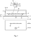
- FIG. 1 schematically shows the components relevant for the position measurement of a position-measuring device according to the invention.
- the basic structure corresponds to the introductory based on the FIG. 3 described position measuring device, which is incorporated herein by reference.
- Components already related to FIG. 3 have been described, carry the same reference numerals.
- the position measuring device comprises a scanning unit 10 and a material measure 40 on which a measuring graduation 41 is arranged.
- the scanning unit 10 consists of a lighting unit 20 known from the prior art and of an inventively improved detector unit 30.
- the decisive improvement of the detector unit 30 could be achieved in that the sensor unit 32, which is designed as a semiconductor chip is not electrically connected by wire bonding to the circuit board 31, but that the terminals of the electrical circuit in the semiconductor chip by means of vias 36 through the semiconductor substrate, from the semiconductor chip is made, are led to contact surfaces 33 on the back of the chip and the electrical connection to corresponding contact surfaces 34 of the circuit board 31 is produced by a soldering process.
- metal beads 37 can first be applied to the contact surfaces 33 of the semiconductor chip, which are then connected by reflow soldering to the corresponding contact surfaces 34 on the printed circuit board 31.
- the elaborate process of wire bonding is thus replaced by a standard soldering process.
- the sensor unit 32 can be placed on the circuit board 31 and soldered simultaneously with the other components in the course of the SMD assembly.
- the front side of a sensor unit 32 designed in this way has a flat surface, which makes the accumulation of dirt particles more difficult in comparison to the sensor unit 532 known from the prior art.
- At least two photodetectors 35 which detect the light of the illumination unit 20 modulated by the measuring graduation 41, are arranged on the front side of the sensor unit 32.
- the actual number of photodetectors 35 depends on the configuration of the measuring graduation 41. If the measuring graduation 41 has more than one graduation track (for example an incremental and, in parallel thereto, one or more absolutely coded graduation tracks), a suitable number of photodetectors 35 are arranged at positions associated with the graduation tracks transversely to the measurement direction X.
- the position signals obtained in this way are processed by a signal processing circuit, which is advantageously integrated partially or completely with the sensor unit 32, and further output to an electronic sequencer (not shown).
- a semiconductor chip comprising both photodetectors and signal processing electronics is an opto-ASIC.
- the printed circuit board 31 can be made of glass fiber reinforced epoxy resin (epoxy), but it can also be used ceramic materials such as alumina.
- the vias 36 are usually applied vertically and made of metal, whereby they have comparable electrical properties, such as the bonding wires used in the prior art.
- the contact surfaces 33 on the semiconductor chip of the sensor unit 32 need not necessarily be arranged directly above the plated-through holes 36. Rather, it is possible that they are arranged offset to one another and connected to each other via a conductor track 38 (redistribution layer).
- the semiconductor chip is based on a silicon substrate, this is also referred to as silicon through-contacts or through-silicon vias (TSV).
- TSV through-silicon vias
- Semiconductor chips with silicon vias are currently used predominantly in image sensors for digital photography, because by laying the contact surfaces on the back of the chip, the usable photosensitive area of the pixels (pixels) can be increased.
- semiconductor chips with silicon vias are used to fabricate 3D integrated circuits (3D-IC) because this interconnect technique is suitable for stacking and interconnecting multiple chips.
- the routing of the contact pads 33 from the front of the sensor unit 32 to the back of the sensor unit 32 allows a sensing distance d defined by the distance of the front of the sensor unit 32 (see FIG. ie, the surface of the semiconductor chip on which the photodetectors are located) to the surface of the measuring graduation 41 (due to the small thickness of the graduation lines in the example shown equates to the surface of the material measure 40), compared to the prior art significantly reduce.
- the sampling distance d is only of assembly tolerances (eg parallelism of the surface of the sensor unit 32 to the surface of the measuring scale 40) and the mechanical guidance of the scanning unit 10, and the sensor unit 32, relative to the material measure 40 dependent. Values of less than 0.55 mm can thus always be selected for the scanning distance d; with a sufficiently precise mechanical structure, even values for the scanning distance d of less than 0.1 mm down to 0.03 mm can be achieved.
- Another advantage resulting from the use of a sensor unit 32 according to the invention is that it is possible to dispense with a scanning plate at a small scanning distance d. This reduces the number of surfaces in the beam path of the light to be detected, whose optical properties can be affected by contamination.
- FIGS. 2a and 2b show the influence of the scanning distance d on the fouling sensitivity of an optical scanning when contaminated by liquid droplets. It is assumed that a liquid droplet 60 is located on the measuring graduation 41. Liquid droplets have a scattering effect on light rays. This results in a blurring in the image of the measuring graduation 41 on the photodetectors 35 (shown are each a central photodetector 35.1 and two adjacent photodetectors 35.2, 35.3), which affects the stronger, the greater the sampling distance d.
- a large sampling distance d causes a significant portion of the scattered light to fall on the adjacent photodetectors 35.2, 35.3. This reduces a position signal detected by the central photodetector 35.1, while the adjacent photodetectors 35.2, 35.3 detect erroneous position signals. Overall, the reliability of the position measurement is compromised.
- a reduction of the scanning distance d, as in FIG. 2b shows that despite scattering of the light, a large portion of the light to be detected falls on the central photodetector 35.1 and only a negligible portion of the scattered light reaches the adjacent photodetectors 35.2, 35.3. This causes a significant increase in the reliability of the position measurement.
- a small sampling distance d also has the effect that larger liquid droplets are compressed between the front of the sensor unit 32 and the surface of the measuring scale 40 and thus form a uniform liquid film, which significantly reduces a scattering of the light. This effect is already effective when the sampling distance d is reduced to less than 0.3 mm.
- the remaining cavity under the sensor unit 32 in an underfill process with an elastic, temperature-resistant plastic material are filled.
- an elastic, temperature-resistant plastic material underfiller 50
- liquid droplets 60 in the range of solder joints between the sensor unit 32 and PCB 31 arrive. Electrical failures caused by fault currents due to an ohmic connection of contacts with electrically conductive liquids, as well as damage to the solder joints by corrosion can be avoided.
- the sensor unit 32 around a side protection 51 made of a plastic material, which protects the side surfaces of the sensor unit 32 from mechanical damage, for example by larger dirt particles.
- the side guard 51 is flush with the edge of the sensor unit 32 associated with the front side.
- FIG. 4a shows an advantageous development of the detector unit 30 FIG. 1 in which the front side of the sensor unit 32 is protected against damage by a protective window 52 made of a suitable transparent material (glass, or the like).
- the connection between the Sensor unit 32 and the protective window 52 can be made by surface bonding or by wringing.
- This construction is particularly easy to produce if in the production of a wafer with a plurality of sensor units 32, this is already connected before sawing off the individual sensor units 32 with a disc made of the material of the protective window 52. Due to the common sawing, the sensor unit 32 and the protective window 52 have the same area. In this case, the side guard 51 can be pulled up so far that it projects beyond the side surfaces of the sensor unit 32 and at least partially covers the side surfaces of the protective window 52. In this way, the sensor unit 32 is fully protected in the fully assembled state of the detector unit 30 from mechanical damage.
- the side shield 51 connects the printed circuit board 31 with the rear side of the protective window 52 facing the sensor unit 32.
- This construction is also easy to produce if the wafer is already connected to the wafer Sensor units 32 and the disc of the material of the protective window 52 are connected to each other and before sowing the sensor units 32, the areas between the sensor units 32 are etched free by an etching process to the disc of the material of the protective window 52.
- the thickness of the protective window can in any case be chosen so that it is less than the height c (approximately 0.5 mm) predetermined by the wire bonding, so that a smaller sampling interval d than the value of 0 specified in the prior art , 55 mm is achievable.
- the thickness of the protective window in the range between 0.2 mm and 0.4 mm, the lower limit can be further reduced by increased effort in manufacturing.
- a graduation structure which fulfills the function of a scanning plate, without the number of contamination exposed, can be arranged on the front side of the protective window 52 facing the measuring graduation 41 Increase surfaces.
- the front side of the sensor unit 32 can be protected from mechanical damage by clear lacquer or clear potting.
Description
Die vorliegende Erfindung betrifft eine Positionsmesseinrichtung nach dem Oberbegriff von Anspruch 1. Derartige Positionsmesseinrichtungen werden vorwiegend in der Automatisierungstechnik zum Messen von Wegen und/oder Winkeln eingesetzt.The present invention relates to a position measuring device according to the preamble of claim 1. Such position measuring devices are mainly used in automation technology for measuring paths and / or angles.
Positionsmesseinrichtungen sind insbesondere bei Werkzeugmaschinen und in der Automatisierungstechnik weit verbreitet. Sie dienen zur Bestimmung der Relativposition zweier zueinander beweglicher Objekte. Dabei unterscheidet man grundsätzlich zwischen Längen- und Winkelmessgeräten. Längenmessgeräte dienen beispielsweise zur Bestimmung der Relativposition zweier zueinander beweglicher Maschinenteile einer Werkzeugmaschine. Hierzu wird eine Maßverkörperung, beispielsweise in Form eines geraden Maßstabs, auf dem eine Messteilung angeordnet ist, mit dem einen und eine Abtasteinheit mit dem anderen der beiden Objekte verbunden, so dass durch Abtasten der Messteilung positionsabhängige Abtastsignale gewonnen werden, mit deren Hilfe sich das Ausmaß der Bewegung der beiden Objekte zueinander in der Bewegungsrichtung bestimmen lässt.Position measuring devices are widely used, in particular, in machine tools and in automation technology. They serve to determine the relative position of two mutually movable objects. In principle, a distinction is made between length and angle encoders. Linear encoders serve, for example, for determining the relative position of two mutually movable machine parts of a machine tool. For this purpose, a material measure, for example in the form of a straight scale, on which a measurement graduation is arranged, connected to the one and a scanning unit with the other of the two objects, so that by scanning the Messteilung position-dependent scanning signals are obtained, with the help of which the extent of movement of the two objects to each other in the direction of movement can be determined.
Winkelmessgeräte, auch unter der Bezeichnung Drehgeber bekannt, sind nach dem gleichen Prinzip aufgebaut. An die Stelle des Maßstabs tritt hier aber als Maßverkörperung eine kreisförmige Scheibe, auf der die Messteilung konzentrisch zum Drehpunkt angeordnet ist. Die Scheibe ist drehfest mit einer zu messenden Welle verbunden, während die Abtasteinheit hierzu fest montiert ist.Angle encoders, also known as encoders, are based on the same principle. Instead of the scale, however, a circular disc appears here as the measuring standard, on which the measuring graduation is arranged concentrically to the point of rotation. The disc is rotatably connected to a shaft to be measured, while the scanning unit is fixedly mounted for this purpose.
Die Messteilung kann eine oder mehrere Teilungsspuren umfassen, wobei inkrementale und absolut codierte Teilungsspuren unterschieden werden. Inkrementale Teilungsspuren bestehen aus regelmäßig angeordneten Teilungselementen, aus deren Abtastung bei gleichförmiger Relativbewegung zwischen Maßverkörperung und Abtasteinheit weitgehend sinusförmige Abtastsignale resultieren. Die Wegbestimmung basiert hier auf der Zählung der Signalperioden oder Bruchteilen von Signalperioden. Für eine absolute Wegbestimmung muss ein Referenzpunkt festgelegt werden, hierfür ist beispielsweise eine Referenzmarke vorgesehen, die ebenfalls von der Abtasteinheit erfasst wird. Aus den Abtastsignalen absolut codierter Teilungsspuren dagegen kann direkt die Absolutposition bestimmt werden, da diese in mehreren, nebeneinander angeordneten Teilungsspuren parallel (z.B. Gray-Code, BCD-Code,...), oder in einer Teilungsspur seriell (z.B. Kettencode, PRC) codiert ist. Darüber hinaus sind auch Messteilungen bekannt, die sowohl inkrementale, als auch absolute Teilungsspuren umfassen.The measurement graduation may comprise one or more graduation tracks, distinguishing incremental and absolutely coded graduation tracks. Incremental graduation tracks consist of regularly arranged graduation elements, the scanning of which results in a uniform relative movement between the measuring standard and the scanning unit resulting in substantially sinusoidal scanning signals. The path determination here is based on the count of the signal periods or fractions of signal periods. For an absolute path determination, a reference point must be determined, for this purpose, for example, a reference mark is provided, which is also detected by the scanning unit. On the other hand, the absolute position can be determined directly from the scanning signals of absolutely coded graduation tracks, since these are coded in a plurality of juxtaposed graduation tracks in parallel (eg gray code, BCD code,...) Or in a graduation track serially (eg chain code, PRC) is. In addition, measuring graduations are also known which comprise both incremental and absolute graduation tracks.
Ein weit verbreitetes Funktionsprinzip bei Positionsmesseinrichtungen ist die optische Abtastung. Dabei wird die Messteilung, die auf einer Maßverkörperung aufgebracht ist, mit gerichtetem Licht, das von einer Lichtquelle abgestrahlt wird, auf eine Anzahl von Fotodetektoren abgebildet. Die Maßverkörperung ist beweglich im Strahlengang des Lichts angeordnet und moduliert das Licht, wenn die Messteilung relativ zur Lichtquelle und den Fotodetektoren bewegt wird. Die Position, bzw. Positionsänderung wird durch Auswertung der Ausgangssignale der Fotodetektoren ermittelt. Die Messteilung kann aus Bereichen mit unterschiedlichen optischen Eigenschaften wie z.B. transparent/opak bestehen.A widely used functional principle in position-measuring devices is optical scanning. In this case, the measurement graduation, which is applied to a material measure, is imaged onto a number of photodetectors using directed light which is emitted by a light source. The material measure is movably arranged in the beam path of the light and modulates the light when the measurement graduation relative to the light source and the photodetectors is moved. The position or position change is determined by evaluating the output signals of the photodetectors. The measurement graduation may consist of areas with different optical properties, such as transparent / opaque.
Die für die Abtastung erforderlichen Fotodetektoren sind meist gemeinsam auf einem Halbleiterchip angeordnet, der mittels Chip-On-Board-Technologie (COB) direkt auf eine Leiterplatte montiert wird. Hierbei wird der Chip mit seiner Rückseite erst auf die Leiterplatte geklebt und anschließend die Kontaktflächen auf seiner Oberseite mittels Drahtbonden an die Leiterplatte angeschlossen. Häufig sind neben den Fotodetektoren auch zumindest Teile der Auswerteelektronik für die Abtastsignale auf dem Halbleiterchip angeordnet.The photodetectors required for scanning are usually arranged together on a semiconductor chip, which is mounted directly on a printed circuit board by means of chip-on-board (COB) technology. In this case, the chip is first glued with its back to the circuit board and then the contact surfaces on its upper side connected by wire bonding to the circuit board. Frequently, at least parts of the evaluation electronics for the scanning signals are arranged on the semiconductor chip in addition to the photodetectors.
Die Abtasteinheit 10 und die Maßverkörperung 40 sind in einer Messrichtung X relativ zueinander beweglich angeordnet. Handelt es sich bei der Positionsmesseinrichtung beispielsweise um eine Einrichtung zur Längenmessung (lineare Positionsmesseinrichtung), so ist die Maßverkörperung 40 als gerader Maßstab ausgeführt, der an einem ersten Maschinenteil befestigt ist und auf dem in Messrichtung X eine Messteilung 41 angeordnet ist. Die Abtasteinheit 10 ist dann an einem zweiten Maschinenteil befestigt und zwar so, dass bei einer Bewegung des ersten Maschinenteils gegenüber dem zweiten Maschinenteil in der Messrichtung X die Abtasteinheit 10 am Maßstab entlang bewegt wird und dabei die Messteilung 41 abtastet. Aus der Abtastung resultieren Abtastsignale, aus denen in weiterer Verarbeitung Positionswerte generiert werden.The scanning unit 10 and the
Bei rotatorischen Positionsmesseinrichtungen (Drehgebern oder Winkelmessgeräten) ist die Maßverkörperung 40 beispielsweise eine kreisrunde Scheibe, die drehfest mit einer Welle, deren Winkelposition gemessen werden soll, verbunden ist. Hier ist die Messteilung 41 konzentrisch zum Drehpunkt der Welle angeordnet. Die Abtasteinheit ist dagegen stationär befestigt und zwar so, dass bei einer Drehung der zu messenden Welle die Messteilung abtastbar ist und aus den Abtastsignalen wiederum Positionswerte, in diesem Fall Winkelwerte, generierbar sind.For rotational position measuring devices (encoders or angle encoders), the
Die Abtasteinheit 10 umfasst eine Beleuchtungseinheit 20 und eine Detektoreinheit 530. Das Funktionsprinzip, das der Positionsmesseinrichtung zugrunde liegt, ist das der optischen Durchlichtabtastung. Das bedeutet, die Messteilung 41 auf der Maßverkörperung 40 ist zwischen der Beleuchtungseinheit 20 und der Detektoreinheit 530 angeordnet. Die Beleuchtungseinheit 20 sendet Licht in Richtung der Messteilung 41 aus. Diese umfasst lichtdurchlässige (transparente) und lichtundurchlässige (opake) Bereiche, die das Licht der Beleuchtungseinheit 20 modulieren. Das modulierte Licht wird auf die Detektoreinheit 530 abgebildet, die hieraus Positionssignale generiert.The scanning unit 10 comprises a lighting unit 20 and a detector unit 530. The operating principle on which the position-measuring device is based is that of the transmitted-light optical scanning. This means that the measuring
In der Praxis wird bei der optischen Durchlichtabtastung bevorzugt parallel ausgerichtetes Licht eingesetzt. Zur Erzeugung von parallel ausgerichtetem Licht kann die Beleuchtungseinheit 20 beispielsweise eine Lichtquelle 21 umfassen, die divergentes Licht aussendet, das von einem Kollimator 22 parallel ausgerichtet wird.In practice, preferably parallel-aligned light is used in the transmitted-light optical scanning. For generating parallel aligned light, the illumination unit 20 may include, for example, a
Die Maßverkörperung 40 besteht mit Vorteil aus einem transparenten Material, beispielsweise Glas. Die Messteilung 41 wird in diesem Fall durch opake Bereiche gebildet, beispielsweise durch Metall, das auf die Maßverkörperung aufgebracht wird. Besonders hierfür geeignet ist beispielsweise Chrom. Es sind aber auch Maßverkörperungen 40 bekannt, die aus einem opaken Material, beispielsweise einem Metall, bestehen. Hier kann die Messteilung 41 als Abfolge von Metallstegen und Durchbrüchen in der Maßverkörperung 40 ausgeführt sein.The
Die Detektoreinheit 530 umfasst eine Leiterplatte 531, eine Sensoreinheit 532 und, insbesondere bei kleinen abzutastenden Teilungsperioden der Messteilung 41, eine Abtastplatte 533.The detector unit 530 comprises a
Die Leiterplatte 531 fungiert unter anderem als Träger für die Sensoreinheit 532, die die zentrale Komponente der Detektoreinheit 530 bildet. Auf der Leiterplatte 531 sind neben unterstützenden elektronischen Schaltungen für die Sensoreinheit 532 beispielsweise Ein-/Ausgabe-Schnittstellen in Form von Steckverbindern etc. angeordnet.The
Die Sensoreinheit 532 ist als Halbleiterchip ausgeführt. Sie weist eine Vorderseite und eine Rückseite auf, wobei die der Leiterplatte 531 zugewandte Seite die Rückseite und die der Messteilung 41 zugewandte Seite die Vorderseite der Sensoreinheit 532 ist. Auf der Vorderseite der Sensoreinheit 532 ist eine Anzahl von Fotodetektoren 535 angeordnet, die zur Erzeugung von Positionssignalen durch Detektion des von der Messteilung 41 und ggf. der Abtastplatte 533 modulierten Lichts der Beleuchtungseinheit 20 dienen. Die Vorderseite der Sensoreinheit 532 ist zu der Ebene, in der sich die Messteilung 41 befindet, vorzugsweise parallel ausgerichtet. Neben den Fotodetektoren 535 umfasst die Sensoreinheit 532 mit Vorteil zusätzliche Komponenten zur Verarbeitung der Positionssignale, ggf. bis hin zur Bildung von Positionswerten aus den Positionssignalen. Darüber hinaus kann die Sensoreinheit eine Vielzahl weiterer Schaltungsblöcke umfassen, wie z.B. Fehlerkorrektur, Schaltungen zur Gewährleistung der Funktionssicherheit, sowie eine digitale Schnittstelle zur Kommunikation mit einer Folgeelektronik. Ein Halbleiterchip, der sowohl Fotodetektoren, als auch Komponenten zur Signalverarbeitung umfasst, wird als Opto-ASIC bezeichnet.The
Die Rückseite der Sensoreinheit 532 ist mit der Leiterplatte 531 verbunden, wobei die Verbindung beispielsweise durch Kleben hergestellt wird. Für die elektrische Verbindung der Schaltungskomponenten der Sensoreinheit 532 mit der Leiterplatte 531 sind auf der Vorderseite der Sensoreinheit 532 und auf der der Sensoreinheit 532 zugewandten Seite der Leiterplatte 531 jeweils korrespondierende Kontaktflächen (nicht dargestellt) angeordnet, die in bekannter Weise durch Drahtbonden über Bonddrähte 537 miteinander verbunden werden. Die Bonddrähte 537 werden durch eine Vergussmasse 538 vor mechanischen Einflüssen geschützt.The rear side of the
Drahtbonden ist ein aufwändiger Fertigungsprozess, sowohl bezogen auf die Anschaffungskosten der erforderlichen Produktionsanlagen (Drahtbonder), als auch auf den zusätzlichen Zeitaufwand für das Drahtbonden, das Vergießen der Bonddrähte und das Aushärten der Vergussmasse.Wire bonding is a complex manufacturing process, both in terms of the cost of the required production equipment (wire bonder), as well as the additional time required for wire bonding, the casting of the bonding wires and the curing of the potting compound.
Resultierend aus dieser Verbindungstechnik ergibt sich ein Damm um die Fotodetektoren, der sich um eine Höhe c bezogen auf die Vorderseite der Sensoreinheit 532 (also der Oberfläche des Halbleiterchips, auf der sich die Fotodetektoren befinden) abhebt. Die Höhe c beträgt bei herkömmlichen Fertigungsverfahren mindestens 0,5 mm. Unter Berücksichtigung von Fertigungstoleranzen, bedingt insbesondere durch Schwankungen in der Dicke der Vergussmasse 538, muss bei diesem Aufbau ein Abtastabstand d, definiert durch den Abstand der Vorderseite der Sensoreinheit 32 (der Oberfläche des Halbleiterchips, auf der sich die Fotodetektoren befinden) zur Oberfläche der Maßverkörperung 40 (im dargestellten Beispiel gleichzusetzen mit der Oberfläche der Messteilung 41), zwischen 0,55 mm und 0,7 mm eingehalten werden, um einen sicheren Betrieb gewährleisten zu können.As a result of this connection technique results in a dam around the photodetectors, which stands for a height c relative to the front of the sensor unit 532 (ie the surface of the semiconductor chip on which the photodetectors are located) lifts. The height c is at least 0.5 mm in conventional manufacturing processes. Taking into account manufacturing tolerances, in particular due to variations in the thickness of the
Die Abtastplatte 533 ist insbesondere bei der Abtastung von kleinen Teilungsperioden notwendig. Sie ist zwischen den Fotodetektoren 535 auf der Vorderseite der Sensoreinheit 532 und der Messteilung 41 angeordnet. Sie weist, ähnlich der Maßverkörperung 40, eine Teilungsstruktur auf, die die Abbildung der Messteilung 41 auf die Fotodetektoren 535 optimiert.The
Die
Es ist offensichtlich, dass sich bei dem optischen Abtastprinzip jegliche Schmutzablagerung im Strahlengang des Lichts nachteilig auf die Funktion auswirkt. Das gilt besonders für flüssige Verschmutzung. Diese tritt in Form von Flüssigkeitströpfchen auf, die beispielsweise aus Schmiermitteln, Kondenswasser, Kühlmittel, etc. bestehen. Sie reduziert nicht nur die auswertbare Lichtmenge, die auf die Fotodetektoren trifft, sondern streut auch noch das Licht, so dass es sich auf mehrere, nebeneinanderliegende Fotodetektoren verteilt.It is obvious that with the optical scanning principle any dirt deposit in the optical path of the light has an adverse effect on the function. This is especially true for liquid pollution. This occurs in the form of liquid droplets, which consist for example of lubricants, condensate, coolant, etc. Not only does it reduce the amount of light that can be applied to the photodetectors, it also disperses light so that it spreads to multiple, adjacent photodetectors.
Der Damm aus Vergussmasse 538 hat bezüglich Schmutzablagerungen negative Eigenschaften, da er, je nach Einbaulage, den Verbleib von Schmutzablagerungen innerhalb des Damms begünstigt.The dam of potting
Um Problemen durch Schmutzablagerungen vorzubeugen, wird bei der Konstruktion von Positionsmesseinrichtungen mit optischer Abtastung besonders darauf geachtet, dass die Einbringung von Schmutzpartikeln, in fester oder auch flüssiger Form, vermieden wird. Dies kann beispielsweise durch die Materialauswahl oder spezielle konstruktive Maßnahmen erfolgen.In order to prevent problems caused by dirt deposits, care is taken in the design of position measuring devices with optical scanning that the introduction of dirt particles, in solid or even liquid form, is avoided. This can be done for example by the selection of materials or special design measures.
Die vollständige Vermeidung einer Verschmutzung ist jedoch schwer möglich. Daher wird versucht, durch Schaffung von Redundanz bei der Abtastung oder durch aufwendige Signalverarbeitung der Abtastsignale den Einfluss von Schmutzpartikeln zu kompensieren.However, avoiding pollution is difficult. Therefore, it is attempted to compensate for the influence of dirt particles by providing redundancy in the sampling or by complex signal processing of the scanning signals.
Trotz all dieser Maßnahmen sind Schmutzpartikel, insbesondere in flüssiger Form, eine mögliche Ausfallursache optischer Positionsmesseinrichtungen.Despite all these measures are dirt particles, especially in liquid form, a possible cause of failure optical position measuring devices.
Es ist daher Aufgabe der Erfindung, eine Positionsmesseinrichtung zu schaffen, die einfach zu Fertigen ist und eine geringe Verschmutzungsempfindlichkeit aufweist.It is therefore an object of the invention to provide a position measuring device which is easy to manufacture and has a low contamination sensitivity.
Diese Aufgabe wird gelöst durch eine Positionsmesseinrichtung nach Anspruch 1. Vorteilhafte Details einer derartigen Positionsmesseinrichtung ergeben sich aus den von Anspruch 1 abhängigen Ansprüchen.This object is achieved by a position-measuring device according to claim 1. Advantageous details of such a position-measuring device result from the claims dependent on claim 1.
Es wird eine Positionsmesseinrichtung vorgeschlagen, umfassend eine Maßverkörperung und eine Abtasteinheit, die in einer Messrichtung relativ zueinander beweglich angeordnet sind, wobei auf der Maßverkörperung eine Messteilung angeordnet ist, die von der Abtasteinheit zur Erzeugung von Positionssignalen abtastbar ist und die Abtasteinheit hierzu eine Beleuchtungseinheit und eine Detektoreinheit umfasst, wobei von der Beleuchtungseinheit Licht in Richtung der Messteilung aussendbar ist und von der Messteilung moduliertes Licht von der Detektoreinheit detektierbar ist und wobei die Detektoreinheit eine Leiterplatte und eine Sensoreinheit umfasst, die als Halbleiterchip ausgebildet ist. Die Erfindung ist dadurch gekennzeichnet, dass auf einer der Messteilung zugewandten Vorderseite der Sensoreinheit wenigstens zwei Fotodetektoren angeordnet sind und die elektrischen Anschlüsse der Sensoreinheit mittels metallischer Durchkontaktierungen zu Kontaktflächen auf deren Rückseite geführt sind und die Sensoreinheit über die Kontaktflächen an korrespondierende Kontaktflächen auf der Leiterplatte angeschlossen ist, wobei ein Abtastabstand zwischen der Vorderseite der Sensoreinheit und der Oberfläche der Messteilung weniger als 0,55 mm beträgt.It is proposed a position measuring device comprising a measuring scale and a scanning unit, which are arranged movable in a measuring direction relative to each other, wherein on the measuring scale a measuring graduation is arranged, which is scanned by the scanning unit for generating position signals and the scanning unit for this purpose, a lighting unit and a Detector unit comprises, wherein from the illumination unit light can be emitted in the direction of the measurement division and modulated by the measurement division light from the detector unit is detectable and wherein the detector unit comprises a circuit board and a sensor unit which is formed as a semiconductor chip. The invention is characterized in that at least two photodetectors are arranged on a front side of the sensor unit facing the measuring graduation and the electrical connections of the sensor unit are guided by means of metallic plated-through holes to contact surfaces on the rear side thereof and the sensor unit is connected via the contact surfaces to corresponding contact surfaces on the printed circuit board wherein a scanning distance between the front of the sensor unit and the surface of the measuring graduation is less than 0.55 mm.
Weitere Vorteile sowie Einzelheiten der vorliegenden Erfindung ergeben sich aus der nachfolgenden Beschreibung anhand der Figuren.Further advantages and details of the present invention will become apparent from the following description with reference to FIGS.
Es zeigt
- Figur 1
- eine schematisch dargestellte erfindungsgemäße Positionsmesseinrichtung,
- Figur 2a
- die durch ein Flüssigkeitströpfchen verursachte Streuung des Lichts bei großem Abtastabstand,
- Figur 2b
- die durch ein Flüssigkeitströpfchen verursachte Streuung des Lichts bei kleinem Abtastabstand,
- Figur 3
- eine schematisch dargestellte Positionsmesseinrichtung entsprechend dem Stand der Technik,
- Figur 4a
- eine vorteilhafte Weiterbildung der Detektoreinheit aus
Figur 1 und - Figur 4b
- eine Variante der Detektoreinheit aus
Figur 4a .
- FIG. 1
- a schematically illustrated position-measuring device according to the invention,
- FIG. 2a
- the scattering of the light caused by a liquid droplet at a large scanning distance,
- FIG. 2b
- the scattering of the light caused by a liquid droplet at a small scanning distance,
- FIG. 3
- a schematically illustrated position measuring device according to the prior art,
- FIG. 4a
- an advantageous development of the detector unit
FIG. 1 and - FIG. 4b
- a variant of the detector unit
FIG. 4a ,
Die Positionsmesseinrichtung umfasst eine Abtasteinheit 10 und eine Maßverkörperung 40, auf der eine Messteilung 41 angeordnet ist. Die Abtasteinheit 10 besteht aus einer aus dem Stand der Technik bekannten Beleuchtungseinheit 20 und aus einer erfindungsgemäß verbesserten Detektoreinheit 30.The position measuring device comprises a scanning unit 10 and a
Die entscheidende Verbesserung der Detektoreinheit 30 konnte dadurch erreicht werden, dass die Sensoreinheit 32, die als Halbleiterchip ausgeführt ist, nicht durch Drahtbonden elektrisch an die Leiterplatte 31 angeschlossen ist, sondern dass die Anschlüsse der elektrischen Schaltung im Halbleiterchip mittels Durchkontaktierungen 36 durch das Halbleitersubstrat, aus dem der Halbleiterchip besteht, zu Kontaktflächen 33 auf der Rückseite des Chips geführt sind und die elektrische Verbindung zu korrespondierenden Kontaktflächen 34 der Leiterplatte 31 über ein Lötverfahren hergestellt wird. Beispielsweise können zuerst auf die Kontaktflächen 33 des Halbleiterchips Metallkügelchen 37 aufgebracht werden, die anschließend durch Reflow-Löten mit den korrespondierenden Kontaktflächen 34 auf der Leiterplatte 31 verbunden werden. Der aufwändige Prozess des Drahtbondens wird also ersetzt durch einen Standard-Lötprozess. Das bedeutet, dass die Sensoreinheit 32 im Zuge der SMD-Bestückung zeitgleich mit den übrigen Komponenten auf der Leiterplatte 31 platziert und gelötet werden kann.The decisive improvement of the
Die Vorderseite einer derart ausgeführten Sensoreinheit 32 weist eine ebene Oberfläche auf, die die Anlagerung von Schmutzpartikeln im Vergleich zu der aus dem Stand der Technik bekannten Sensoreinheit 532 erschwert.The front side of a
Auf der Vorderseite der Sensoreinheit 32 sind wenigstens zwei Fotodetektoren 35 angeordnet, die das von der Messteilung 41 modulierte Licht der Beleuchtungseinheit 20 detektieren. Die tatsächliche Anzahl der Fotodetektoren 35 hängt von der Ausgestaltung der Messteilung 41 ab. Weist die Messteilung 41 mehr als eine Teilungsspur auf (beispielsweise eine inkrementale und, parallel dazu, eine oder mehrere absolut codierte Teilungsspuren), so ist eine geeignete Anzahl von Fotodetektoren 35 an den Teilungsspuren zugeordneten Positionen quer zur Messrichtung X angeordnet. Die so gewonnenen Positionssignale werden von einer Signalverarbeitungsschaltung, die mit Vorteil teilweise oder auch vollständig der Sensoreinheit 32 integriert ist, verarbeitet und weiter an eine Folgeelektronik (nicht dargestellt) ausgegeben. Wie einleitend bereits erwähnt, handelt es sich bei einem Halbleiterchip, der sowohl Fotodetektoren, als auch eine Signalverarbeitungselektronik umfasst, um einen Opto-ASIC.At least two
Die Leiterplatte 31 kann aus glasfaserverstärktem Epoxidharz (Epoxy) bestehen, es können aber auch Keramikwerkstoffe wie beispielsweise Aluminiumoxid zum Einsatz kommen.The printed
Die Durchkontaktierungen 36 sind meist vertikal angelegt und bestehen aus Metall, wodurch sie vergleichbare elektrische Eigenschaften aufweisen, wie die im Stand der Technik verwendeten Bonddrähte. Die Kontaktflächen 33 auf dem Halbleiterchip der Sensoreinheit 32 müssen nicht zwingend direkt über den Durchkontaktierungen 36 angeordnet sein. Vielmehr ist es möglich, dass sie versetzt zueinander angeordnet und über eine Leiterbahn 38 miteinander verbunden sind (Redistribution-Layer).The
Basiert der Halbleiterchip, wie derzeit üblich, auf einem Silizium-Substrat, so spricht man auch von Silizium-Durchkontaktierungen oder Through-Silicon Vias (TSV). Halbleiterchips mit Silizium-Durchkontaktierungen werden derzeit vorwiegend bei Bildsensoren für die Digitalfotografie eingesetzt, weil durch die Verlegung der Kontaktflächen auf die Rückseite des Chips die nutzbare lichtempfindliche Fläche der Bildpunkte (Pixel) vergrößert werden kann. Außerdem kommen Halbleiter-Chips mit Silizium-Durchkontaktierungen zum Einsatz, um 3D-integrierte Schaltkreise (3D-IC) herzustellen, da diese Verbindungstechnik dazu geeignet ist, mehrere Chips übereinander zu stapeln und zu verbinden.If the semiconductor chip, as is currently the case, is based on a silicon substrate, this is also referred to as silicon through-contacts or through-silicon vias (TSV). Semiconductor chips with silicon vias are currently used predominantly in image sensors for digital photography, because by laying the contact surfaces on the back of the chip, the usable photosensitive area of the pixels (pixels) can be increased. In addition, semiconductor chips with silicon vias are used to fabricate 3D integrated circuits (3D-IC) because this interconnect technique is suitable for stacking and interconnecting multiple chips.
Im Hinblick auf die vorliegende Erfindung wurde erkannt, dass es die Verlegung der Kontaktflächen 33 von der Vorderseite der Sensoreinheit 32 auf die Rückseite der Sensoreinheit 32 ermöglicht, einen Abtastabstand d, der im Rahmen dieser Erfindung definiert ist durch den Abstand der Vorderseite der Sensoreinheit 32 (also der Oberfläche des Halbleiterchips, auf der sich die Fotodetektoren befinden) zur Oberfläche der Messteilung 41 (durch die geringe Dicke der Teilungsstriche im dargestellten Beispiel gleichzusetzen mit der Oberfläche der Maßverkörperung 40), gegenüber dem Stand der Technik wesentlich zu verringern. Durch den Wegfall der Bonddrähte 537 und der Vergussmasse 538 (also durch vollständige Eliminierung des Dammes mit der Höhe c) ist der Abtastabstand d nur noch von Aufbautoleranzen (z.B. Parallelität der Oberfläche der Sensoreinheit 32 zur Oberfläche der Maßverkörperung 40) und der mechanischen Führung der Abtasteinheit 10, bzw. der Sensoreinheit 32, gegenüber der Maßverkörperung 40 abhängig. Für den Abtastabstand d können somit in jedem Fall Werte kleiner als 0,55 mm gewählt werden, bei hinreichend genauem mechanischen Aufbau können sogar Werte für den Abtastabstand d von kleiner als 0,1 mm bis hinunter zu 0,03 mm erreicht werden.In view of the present invention, it has been recognized that the routing of the
Weitere elektronische Bauteile, die zusätzlich zur Sensoreinheit 32 benötigt werden, sowie Steckverbinder, etc., sind mit Vorteil auf der Rückseite der Leiterplatte 31 oder in Bereichen, in denen sich die Leiterplatte 31 und die Maßverkörperung 40 im montierten Zustand nicht überlappen, angeordnet.Other electronic components that are required in addition to the
Ein weiterer Vorteil, der sich durch den Einsatz einer erfindungsgemäßen Sensoreinheit 32 ergibt, ist es, dass bei kleinem Abtastabstand d auf eine Abtastplatte verzichtet werden kann. Dadurch verringert sich die Anzahl der Oberflächen im Strahlengang des zu detektierenden Lichts, deren optische Eigenschaften durch Verschmutzung beeinträchtigt werden können.Another advantage resulting from the use of a
Die
Wie in
Eine Verringerung des Abtastabstands d, wie in
Ein kleiner Abtastabstand d hat darüber hinaus den Effekt, dass größere Flüssigkeitströpfchen zwischen der Vorderseite der Sensoreinheit 32 und der Oberfläche der Maßverkörperung 40 zusammengedrückt werden und so einen gleichmäßigen Flüssigkeitsfilm bilden, der eine Streuung des Lichts erheblich reduziert. Dieser Effekt wird bereits wirksam, wenn der Abtastabstand d auf weniger als 0,3 mm reduziert wird.A small sampling distance d also has the effect that larger liquid droplets are compressed between the front of the
Wie in
Weiter ist es vorteilhaft, um die Sensoreinheit 32 herum einen Seitenschutz 51 aus einem Kunststoffmaterial vorzusehen, der die Seitenflächen der Sensoreinheit 32 vor mechanischen Beschädigungen, beispielsweise durch größere Schmutzpartikel, schützt. Mit Vorteil schließt der Seitenschutz 51 mit der der Vorderseite zugehörigen Kante der Sensoreinheit 32 bündig ab.Further, it is advantageous to provide the
Für Seitenschutz 51 und Underfiller 50 kann das gleiche Material eingesetzt werden.For
Dieser Aufbau ist besonders einfach herstellbar, wenn bei der Herstellung eines Wafers mit einer Vielzahl von Sensoreinheiten 32 dieser bereits vor dem Aussägen der einzelnen Sensoreinheiten 32 mit einer Scheibe aus dem Werkstoff des Schutzfensters 52 verbunden wird. Durch das gemeinsame Aussägen weisen Sensoreinheit 32 und Schutzfenster 52 die gleiche Fläche auf. Der Seitenschutz 51 kann in diesem Fall soweit hochgezogen werden, dass er über die Seitenflächen der Sensoreinheit 32 hinaus ragt und die Seitenflächen des Schutzfensters 52 zumindest teilweise bedeckt. Auf diese Weise ist die Sensoreinheit 32 im fertig montierten Zustand der Detektoreinheit 30 allseitig vor mechanischen Beschädigungen geschützt.This construction is particularly easy to produce if in the production of a wafer with a plurality of
Einen noch robusteren Aufbau der Detektoreinheit 30 erhält man, wenn, wie in
Durch das Schutzfenster 52 erhöht sich der minimal erreichbare Abtastabstand d. Die Dicke des Schutzfensters kann aber in jedem Fall so gewählt werden, dass sie geringer als die durch das Drahtbonden vorgegebene Höhe c (ca. 0,5 mm) ist, so dass ein kleinerer Abtastabstand d als der im Stand der Technik vorgegebene Wert von 0,55 mm erreichbar ist. Mit Vorteil liegt die Dicke des Schutzfensters im Bereich zwischen 0,2 mm und 0,4 mm, wobei die untere Grenze durch erhöhten Aufwand in der Fertigung noch weiter verringert werden kann.Through the
Sollte durch den größeren Abtastabstand d in Verbindung mit feinen Teilungsperioden der Messteilung 41 eine Abtastplatte erforderlich werden, so kann auf der der Messteilung 41 zugewandten Vorderseite des Schutzfensters 52 eine Teilungsstruktur angeordnet sein, die die Funktion einer Abtastplatte erfüllt, ohne die Anzahl der einer Verschmutzung ausgesetzten Oberflächen zu erhöhen.Should a scanning plate become necessary due to the larger scanning distance d in conjunction with fine graduation periods of the measuring
Alternativ kann die Vorderseite der Sensoreinheit 32 durch Klarlack oder Klarverguss vor mechanischen Beschädigungen geschützt werden.Alternatively, the front side of the
Claims (9)
- Position measurement device, comprising a material measure (40) and a scanning unit (10), which are arranged to be movable in a measurement direction (X) relative to one another, wherein arranged on the material measure (40) is a measurement graduation (41) which is scannable by the scanning unit (10) for generating position signals and the scanning unit (10) to this end comprises an illumination unit (20) and a detector unit (30), wherein light is emittable by the illumination unit (20) in the direction of the measurement graduation (41) and light which has been modulated by the measurement graduation (41) is detectable by the detector unit (30), and wherein the detector unit (30) comprises a printed circuit board (31) and a sensor unit (32) which is embodied in the form of a semiconductor chip, wherein at least two photodetectors (35) are arranged on a front side of the sensor unit (32) facing the measurement graduation (41), characterized in that the electrical connections of the sensor unit (32) are guided by way of metallic vias (36) to contact surfaces (33) on the rear side thereof and the sensor unit (32) is connected by way of the contact surfaces (33) to corresponding contact surfaces (34) on the printed circuit board (31), wherein a scanning distance (d) between the front side of the sensor unit (32) and the surface of the measurement graduation (41) is less than 0.55 mm.
- Position measurement device according to Claim 1, wherein the remaining hollow space between printed circuit board (31) and sensor unit (32) is filled with an underfill material (50).
- Position measurement device according to either of Claims 1 and 2, wherein a side protection (51) is provided around the sensor unit (32).
- Position measurement device according to one of the preceding claims, wherein the front side of the sensor unit (32) is protected against mechanical damage by a protective window (52) which is connected thereto areally using adhesive bonding or optical contact bonding.
- Position measurement device according to Claim 4, wherein the protective window (52) has the same surface as, or a larger surface than, the sensor unit (32).
- Position measurement device according to either of Claims 4 and 5, wherein a graduation structure is arranged on the side of the protective window (52) facing the measurement graduation (41).
- Position measurement device according to one of Claims 1 to 3, wherein the front side of the sensor unit (32) is protected against mechanical damage by way of clear varnish or clear potting material.
- Position measurement device according to one of the preceding claims, wherein a scanning distance (d) between the front side of the sensor unit (32) and the surface of the measurement graduation (41) is less than 0.3 mm.
- Position measurement device according to one of the preceding claims, wherein the sensor unit (32) is an Opto-ASIC.
Priority Applications (6)
| Application Number | Priority Date | Filing Date | Title |
|---|---|---|---|
| ES15179014T ES2742705T3 (en) | 2015-07-30 | 2015-07-30 | Position measuring device |
| EP15179014.4A EP3124921B1 (en) | 2015-07-30 | 2015-07-30 | Position measuring device |
| DE102016208623.5A DE102016208623A1 (en) | 2015-07-30 | 2016-05-19 | Position measuring device |
| US15/212,943 US10260909B2 (en) | 2015-07-30 | 2016-07-18 | Position measuring device |
| CN201610591470.9A CN106404013B (en) | 2015-07-30 | 2016-07-26 | Position measuring mechanism |
| JP2016149367A JP6889530B2 (en) | 2015-07-30 | 2016-07-29 | Encoder |
Applications Claiming Priority (1)
| Application Number | Priority Date | Filing Date | Title |
|---|---|---|---|
| EP15179014.4A EP3124921B1 (en) | 2015-07-30 | 2015-07-30 | Position measuring device |
Publications (2)
| Publication Number | Publication Date |
|---|---|
| EP3124921A1 EP3124921A1 (en) | 2017-02-01 |
| EP3124921B1 true EP3124921B1 (en) | 2019-05-22 |
Family
ID=53761277
Family Applications (1)
| Application Number | Title | Priority Date | Filing Date |
|---|---|---|---|
| EP15179014.4A Active EP3124921B1 (en) | 2015-07-30 | 2015-07-30 | Position measuring device |
Country Status (6)
| Country | Link |
|---|---|
| US (1) | US10260909B2 (en) |
| EP (1) | EP3124921B1 (en) |
| JP (1) | JP6889530B2 (en) |
| CN (1) | CN106404013B (en) |
| DE (1) | DE102016208623A1 (en) |
| ES (1) | ES2742705T3 (en) |
Families Citing this family (3)
| Publication number | Priority date | Publication date | Assignee | Title |
|---|---|---|---|---|
| DE102016214456A1 (en) * | 2016-08-04 | 2018-02-08 | Dr. Johannes Heidenhain Gesellschaft Mit Beschränkter Haftung | Position measuring device and method for operating a position measuring device |
| JP2019002810A (en) * | 2017-06-15 | 2019-01-10 | 株式会社ミツトヨ | Light receiver and photoelectric encoder having the same |
| EP3657133B1 (en) * | 2018-11-20 | 2021-01-06 | Dr. Johannes Heidenhain GmbH | Sensor unit and position measuring device with this sensor unit |
Family Cites Families (12)
| Publication number | Priority date | Publication date | Assignee | Title |
|---|---|---|---|---|
| DE19855307B4 (en) | 1998-02-20 | 2005-09-29 | Dr. Johannes Heidenhain Gmbh | Scanning unit for an optical position measuring device |
| JP4232301B2 (en) * | 1999-12-14 | 2009-03-04 | ソニー株式会社 | Lead frame manufacturing method and semiconductor device manufacturing method |
| GB0621487D0 (en) * | 2006-10-28 | 2006-12-06 | Renishaw Plc | Opto-electronic read head |
| US8513119B2 (en) * | 2008-12-10 | 2013-08-20 | Taiwan Semiconductor Manufacturing Company, Ltd. | Method of forming bump structure having tapered sidewalls for stacked dies |
| US8212202B2 (en) * | 2009-01-08 | 2012-07-03 | Avago Technologies Ecbu Ip (Singapore) Pte. Ltd. | Reflective optical encoder package and method |
| US9331096B2 (en) * | 2009-09-04 | 2016-05-03 | Luxtera, Inc. | Method and system for hybrid integration of optical communication systems |
| US9057850B2 (en) * | 2011-03-24 | 2015-06-16 | Centera Photonics Inc. | Optoelectronic module |
| US9246601B2 (en) * | 2011-05-03 | 2016-01-26 | Yunzhi Dong | Optical receiver |
| US8829684B2 (en) * | 2011-05-19 | 2014-09-09 | Microsemi Semiconductor Limited | Integrated circuit package |
| EP2693166B1 (en) * | 2012-07-31 | 2015-09-09 | SICK STEGMANN GmbH | Transmission and receiver unit and rotary encoder with such |
| WO2014128796A1 (en) * | 2013-02-25 | 2014-08-28 | パナソニック株式会社 | Semiconductor device |
| TWI571979B (en) * | 2014-11-25 | 2017-02-21 | 彭賢斌 | Integrated passive module, semiconductor device and manufacturing method thereof |
-
2015
- 2015-07-30 ES ES15179014T patent/ES2742705T3/en active Active
- 2015-07-30 EP EP15179014.4A patent/EP3124921B1/en active Active
-
2016
- 2016-05-19 DE DE102016208623.5A patent/DE102016208623A1/en not_active Withdrawn
- 2016-07-18 US US15/212,943 patent/US10260909B2/en active Active
- 2016-07-26 CN CN201610591470.9A patent/CN106404013B/en active Active
- 2016-07-29 JP JP2016149367A patent/JP6889530B2/en active Active
Non-Patent Citations (1)
| Title |
|---|
| None * |
Also Published As
| Publication number | Publication date |
|---|---|
| US10260909B2 (en) | 2019-04-16 |
| DE102016208623A1 (en) | 2017-02-02 |
| JP2017032555A (en) | 2017-02-09 |
| CN106404013B (en) | 2020-08-28 |
| US20170030743A1 (en) | 2017-02-02 |
| JP6889530B2 (en) | 2021-06-18 |
| EP3124921A1 (en) | 2017-02-01 |
| CN106404013A (en) | 2017-02-15 |
| ES2742705T3 (en) | 2020-02-17 |
Similar Documents
| Publication | Publication Date | Title |
|---|---|---|
| DE19843155B4 (en) | Optical displacement measuring device | |
| DE3921756C1 (en) | ||
| WO1999049514A1 (en) | Optoelectronic module | |
| EP3124921B1 (en) | Position measuring device | |
| EP1995566B1 (en) | Measuring rod for a positioning system and positioning system | |
| EP3399284B1 (en) | Sensor unit for position measurement | |
| EP0789228B1 (en) | Opto-electrical position measuring device | |
| EP2063231A2 (en) | Scanning unit of an optical position measuring device and position measuring device with this scanning unit | |
| DE10309679B4 (en) | Scanning unit for scanning a material measure | |
| DE10147987B4 (en) | Optoelectronic component | |
| DE19752511A1 (en) | Scanning unit of optical position measurement device e.g. for flexible printed circuit | |
| DE202017100793U1 (en) | Winkelencoder | |
| EP1377799B1 (en) | Optical position measuring device | |
| EP1141662B1 (en) | Three-dimensional measuring module | |
| WO1999042791A1 (en) | Scanning unit for an optical position measuring device | |
| DE102019119834B4 (en) | ENCODERS | |
| DE102015103253A1 (en) | Optoelectronic component | |
| DE602005004763T2 (en) | Optoelectronic measuring device | |
| EP2823263B1 (en) | Optoelectronic positioning device | |
| DE3126911A1 (en) | Devices for the contactless one- and three-dimensional measurement of jaw or jaw joint movements | |
| DE102006042873A1 (en) | Sensor for determining position of movable object, has light source and photo sensitive detector arranged in fixed manner, and aperture mask arranged together with object in movable manner | |
| EP0993761A1 (en) | Method and device for measuring the height at which object edges of components are positioned | |
| DE102018109615A1 (en) | Sensor chip of a reading head of an optical ruler | |
| DE202018006091U1 (en) | Sensor chip of a reading head of an optical ruler | |
| DE102005043432B4 (en) | Scanning unit of an optical position-measuring device and position-measuring device with this scanning unit |
Legal Events
| Date | Code | Title | Description |
|---|---|---|---|
| PUAI | Public reference made under article 153(3) epc to a published international application that has entered the european phase |
Free format text: ORIGINAL CODE: 0009012 |
|
| STAA | Information on the status of an ep patent application or granted ep patent |
Free format text: STATUS: THE APPLICATION HAS BEEN PUBLISHED |
|
| AK | Designated contracting states |
Kind code of ref document: A1 Designated state(s): AL AT BE BG CH CY CZ DE DK EE ES FI FR GB GR HR HU IE IS IT LI LT LU LV MC MK MT NL NO PL PT RO RS SE SI SK SM TR |
|
| AX | Request for extension of the european patent |
Extension state: BA ME |
|
| STAA | Information on the status of an ep patent application or granted ep patent |
Free format text: STATUS: REQUEST FOR EXAMINATION WAS MADE |
|
| 17P | Request for examination filed |
Effective date: 20170801 |
|
| RBV | Designated contracting states (corrected) |
Designated state(s): AL AT BE BG CH CY CZ DE DK EE ES FI FR GB GR HR HU IE IS IT LI LT LU LV MC MK MT NL NO PL PT RO RS SE SI SK SM TR |
|
| REG | Reference to a national code |
Ref country code: DE Ref legal event code: R079 Ref document number: 502015009112 Country of ref document: DE Free format text: PREVIOUS MAIN CLASS: G01D0005347000 Ipc: G01D0005260000 |
|
| RIC1 | Information provided on ipc code assigned before grant |
Ipc: G01D 5/347 20060101ALI20181107BHEP Ipc: H02S 40/44 20140101ALI20181107BHEP Ipc: G01D 5/26 20060101AFI20181107BHEP Ipc: H01L 31/0203 20140101ALI20181107BHEP |
|
| GRAP | Despatch of communication of intention to grant a patent |
Free format text: ORIGINAL CODE: EPIDOSNIGR1 |
|
| STAA | Information on the status of an ep patent application or granted ep patent |
Free format text: STATUS: GRANT OF PATENT IS INTENDED |
|
| INTG | Intention to grant announced |
Effective date: 20181214 |
|
| GRAS | Grant fee paid |
Free format text: ORIGINAL CODE: EPIDOSNIGR3 |
|
| GRAA | (expected) grant |
Free format text: ORIGINAL CODE: 0009210 |
|
| STAA | Information on the status of an ep patent application or granted ep patent |
Free format text: STATUS: THE PATENT HAS BEEN GRANTED |
|
| AK | Designated contracting states |
Kind code of ref document: B1 Designated state(s): AL AT BE BG CH CY CZ DE DK EE ES FI FR GB GR HR HU IE IS IT LI LT LU LV MC MK MT NL NO PL PT RO RS SE SI SK SM TR |
|
| REG | Reference to a national code |
Ref country code: GB Ref legal event code: FG4D Free format text: NOT ENGLISH |
|
| REG | Reference to a national code |
Ref country code: CH Ref legal event code: EP |
|
| REG | Reference to a national code |
Ref country code: IE Ref legal event code: FG4D Free format text: LANGUAGE OF EP DOCUMENT: GERMAN |
|
| REG | Reference to a national code |
Ref country code: DE Ref legal event code: R096 Ref document number: 502015009112 Country of ref document: DE |
|
| REG | Reference to a national code |
Ref country code: AT Ref legal event code: REF Ref document number: 1136668 Country of ref document: AT Kind code of ref document: T Effective date: 20190615 |
|
| REG | Reference to a national code |
Ref country code: CH Ref legal event code: NV Representative=s name: ICB INGENIEURS CONSEILS EN BREVETS SA, CH |
|
| REG | Reference to a national code |
Ref country code: NL Ref legal event code: MP Effective date: 20190522 |
|
| REG | Reference to a national code |
Ref country code: LT Ref legal event code: MG4D |
|
| PG25 | Lapsed in a contracting state [announced via postgrant information from national office to epo] |
Ref country code: FI Free format text: LAPSE BECAUSE OF FAILURE TO SUBMIT A TRANSLATION OF THE DESCRIPTION OR TO PAY THE FEE WITHIN THE PRESCRIBED TIME-LIMIT Effective date: 20190522 Ref country code: LT Free format text: LAPSE BECAUSE OF FAILURE TO SUBMIT A TRANSLATION OF THE DESCRIPTION OR TO PAY THE FEE WITHIN THE PRESCRIBED TIME-LIMIT Effective date: 20190522 Ref country code: SE Free format text: LAPSE BECAUSE OF FAILURE TO SUBMIT A TRANSLATION OF THE DESCRIPTION OR TO PAY THE FEE WITHIN THE PRESCRIBED TIME-LIMIT Effective date: 20190522 Ref country code: HR Free format text: LAPSE BECAUSE OF FAILURE TO SUBMIT A TRANSLATION OF THE DESCRIPTION OR TO PAY THE FEE WITHIN THE PRESCRIBED TIME-LIMIT Effective date: 20190522 Ref country code: NO Free format text: LAPSE BECAUSE OF FAILURE TO SUBMIT A TRANSLATION OF THE DESCRIPTION OR TO PAY THE FEE WITHIN THE PRESCRIBED TIME-LIMIT Effective date: 20190822 Ref country code: PT Free format text: LAPSE BECAUSE OF FAILURE TO SUBMIT A TRANSLATION OF THE DESCRIPTION OR TO PAY THE FEE WITHIN THE PRESCRIBED TIME-LIMIT Effective date: 20190922 Ref country code: AL Free format text: LAPSE BECAUSE OF FAILURE TO SUBMIT A TRANSLATION OF THE DESCRIPTION OR TO PAY THE FEE WITHIN THE PRESCRIBED TIME-LIMIT Effective date: 20190522 Ref country code: NL Free format text: LAPSE BECAUSE OF FAILURE TO SUBMIT A TRANSLATION OF THE DESCRIPTION OR TO PAY THE FEE WITHIN THE PRESCRIBED TIME-LIMIT Effective date: 20190522 |
|
| PG25 | Lapsed in a contracting state [announced via postgrant information from national office to epo] |
Ref country code: BG Free format text: LAPSE BECAUSE OF FAILURE TO SUBMIT A TRANSLATION OF THE DESCRIPTION OR TO PAY THE FEE WITHIN THE PRESCRIBED TIME-LIMIT Effective date: 20190822 Ref country code: RS Free format text: LAPSE BECAUSE OF FAILURE TO SUBMIT A TRANSLATION OF THE DESCRIPTION OR TO PAY THE FEE WITHIN THE PRESCRIBED TIME-LIMIT Effective date: 20190522 Ref country code: LV Free format text: LAPSE BECAUSE OF FAILURE TO SUBMIT A TRANSLATION OF THE DESCRIPTION OR TO PAY THE FEE WITHIN THE PRESCRIBED TIME-LIMIT Effective date: 20190522 Ref country code: GR Free format text: LAPSE BECAUSE OF FAILURE TO SUBMIT A TRANSLATION OF THE DESCRIPTION OR TO PAY THE FEE WITHIN THE PRESCRIBED TIME-LIMIT Effective date: 20190823 |
|
| PG25 | Lapsed in a contracting state [announced via postgrant information from national office to epo] |
Ref country code: SK Free format text: LAPSE BECAUSE OF FAILURE TO SUBMIT A TRANSLATION OF THE DESCRIPTION OR TO PAY THE FEE WITHIN THE PRESCRIBED TIME-LIMIT Effective date: 20190522 Ref country code: EE Free format text: LAPSE BECAUSE OF FAILURE TO SUBMIT A TRANSLATION OF THE DESCRIPTION OR TO PAY THE FEE WITHIN THE PRESCRIBED TIME-LIMIT Effective date: 20190522 Ref country code: DK Free format text: LAPSE BECAUSE OF FAILURE TO SUBMIT A TRANSLATION OF THE DESCRIPTION OR TO PAY THE FEE WITHIN THE PRESCRIBED TIME-LIMIT Effective date: 20190522 Ref country code: RO Free format text: LAPSE BECAUSE OF FAILURE TO SUBMIT A TRANSLATION OF THE DESCRIPTION OR TO PAY THE FEE WITHIN THE PRESCRIBED TIME-LIMIT Effective date: 20190522 |
|
| REG | Reference to a national code |
Ref country code: ES Ref legal event code: FG2A Ref document number: 2742705 Country of ref document: ES Kind code of ref document: T3 Effective date: 20200217 |
|
| REG | Reference to a national code |
Ref country code: DE Ref legal event code: R097 Ref document number: 502015009112 Country of ref document: DE |
|
| PG25 | Lapsed in a contracting state [announced via postgrant information from national office to epo] |
Ref country code: SM Free format text: LAPSE BECAUSE OF FAILURE TO SUBMIT A TRANSLATION OF THE DESCRIPTION OR TO PAY THE FEE WITHIN THE PRESCRIBED TIME-LIMIT Effective date: 20190522 Ref country code: MC Free format text: LAPSE BECAUSE OF FAILURE TO SUBMIT A TRANSLATION OF THE DESCRIPTION OR TO PAY THE FEE WITHIN THE PRESCRIBED TIME-LIMIT Effective date: 20190522 |
|
| PLBE | No opposition filed within time limit |
Free format text: ORIGINAL CODE: 0009261 |
|
| STAA | Information on the status of an ep patent application or granted ep patent |
Free format text: STATUS: NO OPPOSITION FILED WITHIN TIME LIMIT |
|
| PG25 | Lapsed in a contracting state [announced via postgrant information from national office to epo] |
Ref country code: TR Free format text: LAPSE BECAUSE OF FAILURE TO SUBMIT A TRANSLATION OF THE DESCRIPTION OR TO PAY THE FEE WITHIN THE PRESCRIBED TIME-LIMIT Effective date: 20190522 |
|
| REG | Reference to a national code |
Ref country code: BE Ref legal event code: MM Effective date: 20190731 |
|
| 26N | No opposition filed |
Effective date: 20200225 |
|
| PG25 | Lapsed in a contracting state [announced via postgrant information from national office to epo] |
Ref country code: PL Free format text: LAPSE BECAUSE OF FAILURE TO SUBMIT A TRANSLATION OF THE DESCRIPTION OR TO PAY THE FEE WITHIN THE PRESCRIBED TIME-LIMIT Effective date: 20190522 |
|
| PG25 | Lapsed in a contracting state [announced via postgrant information from national office to epo] |
Ref country code: BE Free format text: LAPSE BECAUSE OF NON-PAYMENT OF DUE FEES Effective date: 20190731 Ref country code: SI Free format text: LAPSE BECAUSE OF FAILURE TO SUBMIT A TRANSLATION OF THE DESCRIPTION OR TO PAY THE FEE WITHIN THE PRESCRIBED TIME-LIMIT Effective date: 20190522 Ref country code: LU Free format text: LAPSE BECAUSE OF NON-PAYMENT OF DUE FEES Effective date: 20190730 |
|
| PG25 | Lapsed in a contracting state [announced via postgrant information from national office to epo] |
Ref country code: FR Free format text: LAPSE BECAUSE OF NON-PAYMENT OF DUE FEES Effective date: 20190731 |
|
| PG25 | Lapsed in a contracting state [announced via postgrant information from national office to epo] |
Ref country code: IE Free format text: LAPSE BECAUSE OF NON-PAYMENT OF DUE FEES Effective date: 20190730 |
|
| PG25 | Lapsed in a contracting state [announced via postgrant information from national office to epo] |
Ref country code: CY Free format text: LAPSE BECAUSE OF FAILURE TO SUBMIT A TRANSLATION OF THE DESCRIPTION OR TO PAY THE FEE WITHIN THE PRESCRIBED TIME-LIMIT Effective date: 20190522 |
|
| PG25 | Lapsed in a contracting state [announced via postgrant information from national office to epo] |
Ref country code: IS Free format text: LAPSE BECAUSE OF FAILURE TO SUBMIT A TRANSLATION OF THE DESCRIPTION OR TO PAY THE FEE WITHIN THE PRESCRIBED TIME-LIMIT Effective date: 20190922 |
|
| PG25 | Lapsed in a contracting state [announced via postgrant information from national office to epo] |
Ref country code: MT Free format text: LAPSE BECAUSE OF FAILURE TO SUBMIT A TRANSLATION OF THE DESCRIPTION OR TO PAY THE FEE WITHIN THE PRESCRIBED TIME-LIMIT Effective date: 20190522 Ref country code: HU Free format text: LAPSE BECAUSE OF FAILURE TO SUBMIT A TRANSLATION OF THE DESCRIPTION OR TO PAY THE FEE WITHIN THE PRESCRIBED TIME-LIMIT; INVALID AB INITIO Effective date: 20150730 |
|
| REG | Reference to a national code |
Ref country code: AT Ref legal event code: MM01 Ref document number: 1136668 Country of ref document: AT Kind code of ref document: T Effective date: 20200730 |
|
| PG25 | Lapsed in a contracting state [announced via postgrant information from national office to epo] |
Ref country code: AT Free format text: LAPSE BECAUSE OF NON-PAYMENT OF DUE FEES Effective date: 20200730 |
|
| PG25 | Lapsed in a contracting state [announced via postgrant information from national office to epo] |
Ref country code: MK Free format text: LAPSE BECAUSE OF FAILURE TO SUBMIT A TRANSLATION OF THE DESCRIPTION OR TO PAY THE FEE WITHIN THE PRESCRIBED TIME-LIMIT Effective date: 20190522 |
|
| PGFP | Annual fee paid to national office [announced via postgrant information from national office to epo] |
Ref country code: IT Payment date: 20230724 Year of fee payment: 9 Ref country code: GB Payment date: 20230721 Year of fee payment: 9 Ref country code: ES Payment date: 20230926 Year of fee payment: 9 Ref country code: CZ Payment date: 20230721 Year of fee payment: 9 Ref country code: CH Payment date: 20230801 Year of fee payment: 9 |
|
| PGFP | Annual fee paid to national office [announced via postgrant information from national office to epo] |
Ref country code: DE Payment date: 20230719 Year of fee payment: 9 |