EP3123976A1 - Lichthärtgerät - Google Patents
Lichthärtgerät Download PDFInfo
- Publication number
- EP3123976A1 EP3123976A1 EP15179313.0A EP15179313A EP3123976A1 EP 3123976 A1 EP3123976 A1 EP 3123976A1 EP 15179313 A EP15179313 A EP 15179313A EP 3123976 A1 EP3123976 A1 EP 3123976A1
- Authority
- EP
- European Patent Office
- Prior art keywords
- light curing
- curing apparatus
- reflector body
- reflector
- led chips
- Prior art date
- Legal status (The legal status is an assumption and is not a legal conclusion. Google has not performed a legal analysis and makes no representation as to the accuracy of the status listed.)
- Granted
Links
Images

Classifications
-
- A—HUMAN NECESSITIES
- A61—MEDICAL OR VETERINARY SCIENCE; HYGIENE
- A61C—DENTISTRY; APPARATUS OR METHODS FOR ORAL OR DENTAL HYGIENE
- A61C19/00—Dental auxiliary appliances
- A61C19/003—Apparatus for curing resins by radiation
Definitions
- the invention relates to a light curing apparatus, according to the preamble of claim 1.
- Such a light curing device is from the EP 2 332 490 known.
- a substrate is provided as the basis for receiving LED chips. This is used for heat dissipation, but also the attachment of electrical connections with the LED chips.
- Each chip has a reflection element which, in a manner known per se, extends from the chip in the direction of the light emission.
- the chips heat up with light emission, which is accompanied by heat emission, and thus the reflector body. Via an expansion gap between the individual reflection elements of the reflectors, there is the possibility that they each extend symmetrically.
- Reflector bodies have therefore also been proposed which extend in a hexagonal arrangement relative to one another in order to achieve the best possible light emission; In such a light curing device, the arrangement of the chips is first mounted, and then subsequently the reflector body is placed in one go.
- the invention has for its object to provide a light curing apparatus according to the preamble of claim 1, which is further improved in terms of flexibility at still lower production costs, but at least constant optical quality.
- the inventive feature is connected to the reinforcing walls or a reinforcing ring surrounding a common reflector body with reflection elements.
- the reflection elements themselves are closely adjacent; they can even cut themselves.
- the annular, in particular circular ring-shaped reinforcing wall is prevented as it were, that the reflection elements "move apart" when heated and move their optical axes to the outside.
- the reinforcing wall is on the one hand quite far away from the heat source LED chip, and on the other hand, it extends freely obliquely upward into the room, so that there is a certain cooling there.
- the slots according to the EP 2 332 491 can thus be avoided without sacrificing quality, and the production is significantly cheaper, since instead of three injection molded parts only one injection molded part must be made.
- sensors can also be accommodated particularly favorably in the reflector body, namely at the outer corners of the partition walls or between these and the reinforcing wall.
- a three-leaf cloverleaf or a four-leaf clover shape is selected for the arrangement of the reflection elements - always a sufficient space before, and the sensor openings, which are provided between the reinforcing wall and the cloverleaf, additionally allow the passage of air, which contributes to the further cooling of the reinforcing wall.
- reinforcing wall is mentioned here as an essential element, it is understood that this does not have to be drawn to the height of the LED chips; insofar as the reinforcing wall could also be referred to as a reinforcing ring, which terminates preferably with the upper level of the reflectors.
- annular configuration with respect to the partitions significantly reduced height also allows a further thermal separation of the substrate and the LED chips as heat sources.
- the reflector body according to the invention can be manufactured relatively inexpensively and mirrored in a conventional manner after completion of the injection molding process inside. He is also flexible, because the recesses provided allow it in a budget version, for example, only two opposing reflectors to equip with LED chips. At higher power, a third LED chip can be added, and with further increased power a fourth, for example with a different emission wavelength.
- a central LED chip can also be added, that is to say in the center of the cloverleaf, below a corresponding passage opening.
- This LED chip can emit, for example, with an emission maximum that is different from the emission maximum of the remaining LED chips.
- sensors are then provided below the indentations of the cloverleaf. These serve to detect radiation to be hardened by the dental restoration part or other objects, in order to favorably influence the control of the light curing device overall.
- a four-leaf clover for example, can accommodate three LED chips that emit with high power and emission maximum, which is in the blue light range, another LED chip in the fourth leaf of the cloverleaf, which also emits high power with a violet emission maximum , and a fifth LED chip in the central aperture, which emits in a green emission maximum with lower power.
- the solution according to the invention with the special reflector body is a flexible and suitable for different light curing devices and inexpensive reflector body.
- converging lenses are provided in each reflector or at least one of the reflectors, which cover the LED chips ever.
- the converging lenses can be realized in such a way that they are already mounted on the printed circuit board together with the associated LED chips and also cover the LED chip over a large area on this printed circuit board.
- the condenser lens then becomes comparatively hot, even if it is made of plastic.
- the converging lens is separated by a gap from the associated reflector, which further contributes to the fact that the reflector deforms only slightly,
- the in Fig. 1 illustrated reflector body 10 is part of a light curing device, not otherwise mentioned.
- the reflector body 10 is preferably made of black plastic and provided on its inside at the Refiekomseiementen with an HR layer with high reflection efficiency.
- the HR layer is tuned to the emitted wavelength.
- the reflector body 10 is located at the interface between light sources and a light guide rod, as is better Fig. 3 can be seen in the handpiece of the light curing device.
- it is located at the tip of a wand intended to be inserted into the mouth of a patient and there emit light radiation for hardening dental restorations in front of the corresponding light sources mounted on the tip of the bar.
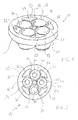
- the reflector body 10 is basically, so from the outer shape ago, circular, and thus extends around a central axis 12. It has a plurality of reflection elements, of which four reflection elements 14 to 20 are provided in the example case. These extend in the manner of a four-leaf clover and terminate flush with a front surface 22. Together with associated, from Fig. 1 not apparent collecting lenses each reflection element 14 to 20 forms a reflector, which is exemplified here as a reflector 24.
- the reflection elements 14 to 20 and thus the associated reflectors 20, 22, 24 are formed evenly distributed in the front view, including on Fig. 2 to refer, which shows the front view of the reflector body 10.
- the reflectors and the associated reflection elements in principle adjoin one another, but are each separated from one another via partitions 30, 32, 34 and 36. This means that the cones do not intersect but are closely adjacent. In particular, the distance is significantly less than the diameter of each cone on the front surface 22.
- all reflectors and reflection elements are part of the common reflector body. This is surrounded by a reinforcing ring 40, which could also be considered as a reinforcing wall.
- the reinforcing ring 40 extends in an annular manner around all the reflection elements 14 to 20 and, to that extent, adjoins them externally.
- the strength of the reinforcing ring viewed in the radial direction is significantly more than the thickness of the partition walls 30 to 36, for example, five times. It is also between 50% and 100% of the radius of a reflection element and therefore represents a solid ring, which holds this stable even when deformation of the "inner life" of the reflector.
- the reinforcing ring 40 accordingly stiffens the thin-walled reflection element arrangement such that the optical axes of the reflection elements do not diverge from one another even when the reflection elements are heated.
- a central aperture 50 is provided, which extends in the "middle" of the cloverleaf around the central axis 12 around. This opening serves the passage of light of a central LED chip, which can have an emission maximum in the green wavelength range.
- the minor wavelength range may be selectively and beneficially green and used for detecting the position of the photocuring apparatus depending on the result of the reflection on a surface of a dental restoration.
- Fig. 4 To detect the reflected radiation, sensors are provided which are made Fig. 4 can be seen. Openings 52, 54, 56 and 58 are provided along the outer periphery of the reflector body 10, but within the reinforcing ring 40, to transmit light to the sensors.
- the naturalb rougeen 52 to 58 have the Fig. 1 and 2 apparent special shape, which is based on the other hand on the outer circumference of the reflection elements on the one hand and on the inner circumference of the reinforcing ring 40 on the other hand.
- the reinforcing ring 40 is missing in the region of the perforations 52 to 58, so that a plurality of reinforcing walls 40 are present on the reflection elements 14 to 20 and, instead of the apertures, depressions are provided with otherwise the same shape.
- Fig. 2 It can be seen that converging lenses 60, 62 and 64 in front of three LED chips can be arranged in the associated reflection elements 14, 16 and 20, which are quite compact and extend in front of LED chips emitting in the main wavelength range with blue emission maximum.
- the fourth LED chip emits in a wavelength range with an emission maximum lying in the violet wavelength range and is covered by a converging lens 66.
- a light guide rod 70 extends in front of the light source 72, which has inter alia LED chips 74 and 76.
- the light source 72 also includes the central LED chip 78 extending in the middle of the cloverleaf array.
- the LED chips are arranged on a plated-through printed circuit board 80.
- the printed circuit board 80 has a high copper content and thick vias, so that the heat can be dissipated well to a heat sink, not shown.
- sensors are arranged, of which two sensors 82 and 84 from Fig. 3 can be seen.
- the sensors extend behind the openings 52 and 56.
- the LED chips 74 to 78 emit transmitted light 89 to the distal end 88 of the light guide rod 70. There, the emitted light leaves the light guide rod 70 and strikes a dental restoration part 90. There it is at least partially reflected. As receiving light 92, it enters again into the light guide rod and through the openings 52 and 56 it falls on the sensors 82 and 84, via which an evaluation takes place.
- a light mixing body 94 may be integrally provided in the light guide rod 70 which is disposed adjacent to the reflector body 10.
- Fig. 4 shows a perspective view of the printed circuit board 80 with mounted LED chips, sensors 82 and 84 and the reflector body 10. About mounting holes 94, the printed circuit board 70 is securely attached to the light curing device 80.
- the light guide rod 70 is preferably detachably mounted in the Lichhärt réelle otherwise. This is done via known per se, but not shown here clamping fasteners, so that the light guide rod including the light mixing body is removable and autoclavable if necessary.
- a part of a reflection element 14 is shown, in combination with the associated condenser lens 60 and the associated LED chips 74. It can be seen that the reflector body 10 projects beyond the outer periphery of the condenser lens 60. However, there is specifically provided a gap 100 between the reflector body 14 and the condenser lens 60, which provides thermal insulation insofar. The heat emitted by chip 74 is therefore predominantly dissipated via the printed circuit board 80.
Landscapes
- Health & Medical Sciences (AREA)
- Oral & Maxillofacial Surgery (AREA)
- Dentistry (AREA)
- Epidemiology (AREA)
- Life Sciences & Earth Sciences (AREA)
- Animal Behavior & Ethology (AREA)
- General Health & Medical Sciences (AREA)
- Public Health (AREA)
- Veterinary Medicine (AREA)
- Led Device Packages (AREA)
Description
- Die Erfindung betrifft ein Lichthärtgerät, gemäß dem Oberbegriff von Anspruch 1.
- Ein derartiges Lichthärtgerät ist aus der
EP 2 332 490 bekannt. Bei einem derartigen Lichthärtgerät ist ein Substrat als Basis für die Aufnahme von LED-Chips vorgesehen. Dieses dient der Wärmeableitung, aber auch der Anbringung von elektrischen Verbindungen mit den LED-Chips. - Jeder Chip weist ein Reflektionselement auf, der sich in an sich bekannter Weise von dem Chip ausgehend in Richtung der Lichtabgabe erstreckt.
- Die Chips erwärmen sich bei Lichtemission, die mit Wärmeemission einhergeht, und damit auch die Reflektorkörper. Über einen Dehnungsspalt zwischen den einzelnen Reflektionselementen der Reflektoren besteht die Möglichkeit, dass diese sich je symmetrisch ausdehnen.
- Diese Lösung ist zwar im Grunde optisch gut, jedoch bedarf sie einer exakten Montage, um den im Submillimeter-Bereich vorgesehenen Spalt zwischen den Reflektoren tatsächlich zu realisieren. Zudem ist diese Lösung ausgesprochen komplex, wenn deutlich mehr als 3 LED-Chips vorgesehen sein sollen.
- Es sind daher auch Reflektorkörper vorgeschlagen worden, die sich in Hexagonal-Anordnung zueinander erstrecken, um eine möglichst dichte Lichtemission zu erreichen; bei einem derartigen Lichthärtgerät wird zunächst die Anordnung der Chips montiert, und hieran anschließend wird in einem Zuge der Reflektorkörper aufgesetzt.
- Auch hier muss jedoch dafür Sorge getragen werden, dass die Ausrichtung zwischen Reflektorkörper und den einzelnen LED-Chips in sich stimmt.
- Es ist auch bereits vorgeschlagen worden, einzelne Einzelreflektoren in einem aus Metall bestehenden Substratkörper vorzusehen. Dies führt zwar dazu, dass sich nur unwesentliche Verformungen einstellen, die die Ausrichtung der optischen Achse der einzelnen Reflektoren praktisch nicht beeinflussen. Nachteilig ist jedoch der vergleichsweise hohe Aufwand und die geringe Flexibilität, denn für jedes Lichthärtgerät bzw. jede Art des Lichthärtgeräts muss ein spezieller Substratkörper aus dem Vollen gefertigt werden, wobei für die spanabhebende Bearbeitung typischerweise zwei unterschiedliche Arten von Werkzeugmaschinen eingesetzt werden müssen, nämlich eine Drehmaschine und eine Fräsmaschine. Dennoch ist die Qualität gedrehter Reflektoren vergleichsweise schlecht, auch wenn im Nachhinein eine entsprechende Überschutzschicht, beispielsweise durch Verchromen, hergestellt ist.
- Von der Flexibilität her, aber auch von der Qualität der Reflexion und der optischen Ausrichtung sind daher demgegenüber Lösungen gemäß der
EP 2 332 491 überlegen. - Demgegenüber liegt jedoch der Erfindung die Aufgabe zugrunde, ein Lichthärtgerät gemäß dem Oberbegriff von Anspruch 1 zu schaffen, das hinsichtlich der Flexibilität bei dennoch geringeren Fertigungskosten, aber mindestens gleichbleibender optischer Qualität weiter verbessert ist.
- Diese Aufgabe wird erfindungsgemäß durch Anspruch 1 gelöst. Vorteilhafte Weiterbildungen ergeben sich aus den Unteransprüchen.
- Die erfindungsgemäße Besonderheit ist mit den Verstärkungswänden oder einem Verstärkungsring verbunden, die einen gemeinsamen Reflektorkörper mit Reflektionselementen umgeben. Die Reflektionselemente selbst sind eng benachbart; sie können sich sogar schneiden. Durch die ringförmige, insbesondere kreisringsförmige Verstärkungswand wird gleichsam verhindert, dass sich die Reflektionselemente bei Erwärmung "auseinander bewegen" und sich ihre optischen Achsen nach außen verlagern. Die Verstärkungswand ist zum einen recht weit entfernt von der Wärmequelle LED-Chip, und zum anderen erstreckt sie sich frei schräg nach oben hin in den Raum hinein, so dass auch eine gewisse Kühlung dort gegeben ist. Die Spielschlitze gemäß der
EP 2 332 491 lassen sich so ohne Qualitätseinbußen vermeiden, und die Fertigung ist deutlich kostengünstiger, da statt dreier Spritzgussteile lediglich ein Spritzgussteil gefertigt werden muss. - In vorteilhafter Ausgestaltung lassen sich zudem besonders günstig auch Sensoren in dem Reflektorkörper unterbringen, nämlich an den Außenecken der Trennwände bzw. zwischen diesen und der Verstärkungswand. Dort liegt - egal ob beispielsweise eine Dreier-Kleeblattform oder eine Vierer-Kleeblattform für die Anordnung der Reflektionselemente gewählt ist - stets ein ausreichender Freiraum vor, und die Sensoröffnungen, die zwischen der Verstärkungswand und dem Kleeblatt vorgesehen sind, ermöglichen zusätzlich das Durchtreten von Luft, was zur weiteren Kühlung der Verstärkungswand beiträgt.
- Auch wenn hier eine Verstärkungswand als wesentliches Element angesprochen ist, versteht es sich, dass diese nicht bis zu der Höhe der LED-Chips gezogen werden muss; insofern könnte die Verstärkungswand auch als Verstärkungsring bezeichnet werden, der bevorzugt mit der oberen Ebene der Reflektoren abschließt.
- Die ringförmige Ausgestaltung mit gegenüber den Trennwänden deutlich reduzierter Bauhöhe erlaubt auch eine weitere thermische Trennung von dem Substrat und den LED-Chips als Wärmequellen.
- Der erfindungsgemäße Reflektorkörper lässt sich vergleichsweise preisgünstig fertigen und in an sich bekannter Weise nach Abschluss des Spritzgussverfahrens innen verspiegeln. Er ist auch flexibel, denn die vorgesehenen Ausnehmungen erlauben es bei einer preisgünstigen Version, beispielsweise lediglich zwei einander gegenüberliegende Reflektoren mit LED-Chips zu bestücken. Bei höherer Leistung kann ein dritter LED-Chip hinzugefügt werden, und bei weiter erhöhter Leistung ein vierter, beispielsweise mit einer anderen Emissionswellenlänge.
- In einer weiteren Ausbaustufe kann auch ein zentraler LED-Chip hinzugefügt werden, also im Zentrum des Kleeblatts, unterhalb einer entsprechenden Durchtrittsausnehmung. Dieser LED-Chip kann beispielsweise mit einem Emissionsmaximum emittieren, das von dem Emissionsmaximum der übrigen LED-Chips verschieden ist. In der maximalen Ausbaustufe sind dann Sensoren unterhalb der Einbuchtungen des Kleeblatts vorgesehen. Diese dienen dazu, von dem zu härtenden Dentalrestaurationsteil oder von anderen Gegenständen reflektierte Strahlung zu erfassen, um die Steuerung des Lichthärtgeräts insgesamt günstig zu beeinflussen.
- Bei einem vierblättrigen Kleeblatt lassen sich daher beispielsweise drei LED-Chips unterbringen, die mit großer Leistung und einem Emissionsmaximum emittieren, das im blauen Lichtbereich liegt, ein weiterer LED-Chip im vierten Blatt des Kleeblatts, der ebenfalls mit großer Leistung mit einem violetten Emissionsmaximum emittiert, und ein fünfter LED-Chip in der zentralen Öffnung, der in einem grünem Emissionsmaximum mit geringerer Leistung emittiert.
- Insofern stellt die erfindungsgemäße Lösung mit dem besonderen Reflektorkörper einen flexiblen und für unterschiedliche Lichthärtgeräte geeigneten und preisgünstigen Reflektorkörper dar.
- In weiterer vorteilhafter Ausgestaltung ist es vorgesehen, dass Sammellinsen in jedem Reflektor oder mindestens einem der Reflektoren vorgesehen sind, die die LED-Chips je abdecken. Die Sammellinsen können so realisiert sein, dass sie zusammen mit den zugehörigen LED-Chips bereits auf der Printplatte montiert sind und auf dieser Printplatte ebenfalls großflächig den LED-Chip umgebend aufliegen. Die Sammellinse wird dann vergleichsweise heiß, auch wenn sie aus Kunststoff besteht. In diesem Zusammenhang ist es dann günstig, wenn die Sammellinse durch einen Spalt von dem zugehörigen Reflektor getrennt ist, was weiter dazu beiträgt, dass der Reflektor sich nur wenig verformt,
- Weitere Vorteile, Einzelheiten und Merkmale ergeben sich aus der nachfolgenden Beschreibung eines Ausführungsbeispiels der Erfindung anhand der Zeichnungen. Es zeigen:
- Fig. 1
- eine schematische Ansicht eines erfindungsgemäßen Lichthärtgeräts in einem Detail, nämlich dem erfindungsgemäßen Reflektorkörper;
- Fig. 2
- den Reflektorkörper in der Ausfürungsform gemäß
Fig. 1 , jedoch in der Draufsicht; - Fig. 3
- ein weiteres Detail eines erfindungsgemäßen Lichthärtgeräts, nämlich den Lichtleitstab in Kombination mit den Lichtquellen, dem Reflektorkörper und auch in der Anwendung an einem Dentalrestaurationsteil;
- Fig. 4
- den erfindungsgemäßen Reflektorkörper, montiert auf einer Printplatte;
- Fig. 5
- ein Detail des Reflektorkörpers und der Printplatte.
- Der in
Fig. 1 dargestellte Reflektorkörper 10 ist Teil eines im Übrigen nicht dargestellten Lichthärtgeräts. Der Reflektorkörper 10 ist vorzugsweise aus schwarzem Kunststoff und an seiner Innenseite an den Refiektionseiementen mit einer HR-Schicht mit hohem Reflexionswirkungsgrad versehen. Die HR-Schicht ist auf die emittierte Wellenlänge abgestimmt. Der Reflektorkörper 10 befindet sich an der Schnittstelle zwischen Lichtquellen und einem Lichtleitstab, wie es besser ausFig. 3 ersichtlich ist, in dem Handstück des Lichthärtgeräts. - In anderer Ausgestaltung befindet er sich an der Spitze eines Stabs, der dafür bestimmt ist, in den Mund eines Patienten eingeführt zu werden und dort Lichtstrahlung zum Härten von Dentalrestaurationen abzugeben, vor den entsprechenden Lichtquellen, die an der Spitze des Stabs montiert sind.
- Der Reflektorkörper 10 ist im Grunde, also von der Außenform her, kreisförmig, und erstreckt sich insofern um eine Zentralachse 12. Er weist eine Mehrzahl von Reflektionselementen auf, von denen im Beispielsfalle vier Reflektionselemente 14 bis 20 vorgesehen sind. Diese erstrecken sich nach der Art eines vierblättrigen Kleeblatts und enden bündig an einer Vorderfläche 22. Zusammen mit zugehörigen, aus
Fig. 1 nicht ersichtlichen Sammellinsen bildet jedes Reflektionselement 14 bis 20 einen Reflektor, der hier beispielhaft als Reflektor 24 bezeichnet sei. - Die Reflektionselemente 14 bis 20 und damit die zugehörigen Reflektoren 20, 22, 24 sind in der Stirnansicht gleichmäßig verteilt ausgebildet, wozu auch auf
Fig. 2 zu verweisen ist, die die Stirnansicht des Reflektorkörpers 10 zeigt. - Die Reflektoren und die zugehörigen Reflektionselemente grenzen grundsätzlich aneinander an, sind jedoch über Trennwände 30, 32, 34 und 36 je voneinander getrennt. Dies bedeutet, dass die Kegel einander nicht schneiden, aber eng benachbart sind. Insbesondere beträgt der Abstand deutlich weniger als der Durchmesser jedes Kegels an der Vorderfläche 22.
- Erfindungsgemäß sind sämtliche Reflektoren und Reflektionselemente Teil des gemeinsamen Reflektorkörpers. Dieser ist mit einem Verstärkungsring 40 umgeben, der auch als Verstärkungswand betrachtet werden könnte. Der Verstärkungsring 40 verläuft kreisringförmig um alle Reflektionselemente 14 bis 20 herum und grenzt insofern außen an diese an.
- Die Stärke des Verstärkungsrings in radialer Richtung betrachtet beträgt deutlich mehr als die Stärke der Trennwände 30 bis 36, beispielsweise das Fünffache. Sie beträgt auch zwischen 50% und 100% des Radius eines Reflektionselements und stellt daher einen massiven Ring dar, der auch bei Verformung des "Innenlebens" des Reflektors diesen außen stabil hält.
- Aufgrund dieser Konfiguration ist es erfindungsgemäß möglich, mit einem einstückigen Reflektor zu der nahezu gleichen Ausschaltung der Parallaxenfehler zu kommen wie beim vorstehend erwähnten Stand der Technik.
- Der Verstärkungsring 40 steift dementsprechend die dünnwandige Reflektionselementanordnung derart aus, dass die optischen Achsen der Reflektionselemente auch bei Erwärmung der Reflektionselemente nicht voneinander divergieren.
- In der in
Fig. 1 dargestellten Ausführungsform ist eine zentrale Durchbrechung 50 vorgesehen, die sich in der "Mitte" des Kleeblatts um die Zentralachse 12 herum erstreckt. Diese Durchbrechung dient dem Lichtdurchlass eines zentralen LED-Chips, der ein Emissionsmaximum im grünen Wellenlängenbereich haben kann. - Der Nebenwellenlängenbereich kann gezielt und günstigerweise grün sein und für die Erfassung der Position des Lichthärtgeräts in Abhängigkeit von dem Reflexionsergebnis auf einer Oberfläche einer Dentalrestauration verwendet werden.
- Um die reflektierte Strahlung zu erfassen, sind Sensoren vorgesehen, die aus
Fig. 4 ersichtlich sind. Durchbrechungen 52, 54, 56 und 58 sind entlang des Außenumfangs des Reflektorkörpers 10, jedoch innerhalb des Verstärkungsrings 40 vorgesehen, um Licht zu den Sensoren durchzulassen. Die Durchbrechnungen 52 bis 58 weisen die ausFig. 1 und 2 ersichtliche besondere Form auf, die sich an den Außenumfang der Reflektionselemente einerseits und an den Innenumfang des Verstärkungsrings 40 andererseits anlehnt. - In einer modifizierten Ausführungsform fehlt der Verstärkungsring 40 im Bereich der Durchbrechungen 52 bis 58, so dass mehrere Verstärkungswände 40 an den Reflektionselementen 14 bis 20 vorliegen und anstelle der Durchbrechungen Einbuchtungen mit im Übrigen gleicher Form vorgesehen sind.
- Aus
Fig. 2 ist ersichtlich, dass Sammellinsen 60, 62 und 64 vor drei LED-Chips in den zugehörigen Reflektionselementen 14, 16 und 20 angeordnet sein können, die recht kompakt sind, und sich vor LED-Chips erstrecken, die im Hauptwellenlängenbereich mit blauem Emissionsmaximum emittieren. - Der vierte LED-Chip emittiert in einem Wellenlängenbereich mit einem Emissionsmaximum, das im violetten Wellenlängenbereich liegt und ist von einer Sammellinse 66 abgedeckt.
- Aus
Fig. 3 ist ersichtlich, in welcher Weise sich ein Lichtleitstab 70 vor der Lichtquelle 72, die unter anderem LED-Chips 74 und 76 aufweist, erstreckt. - Die Lichtquelle 72 umfasst auch den zentralen LED-Chip 78, der sich in der Mitte der Kleeblattanordnung erstreckt.
- Die LED-Chips sind auf einer durchkontaktierten Printplatte 80 angeordnet. Die Printplatte 80 hat einen hohen Kupferanteil und dicke Durchkontaktierungen, so dass die Wärme gut zu einem nicht dargestellten Kühlkörper ableitbar ist.
- Am Außenumfang des Bereichs der Lichtquelle 72 sind Sensoren angeordnet, von denen zwei Sensoren 82 und 84 aus
Fig. 3 ersichtlich sind. Die Sensoren erstrecken sich hinter den Durchbrechungen 52 und 56. - Wie in
Fig. 3 gestrichelt dargestellt ist, emittieren die LED-Chips 74 bis 78 Sendelicht 89 zum distalen Ende 88 des Lichtleitstabs 70. Dort verlässt das emittierte Licht den Lichtleitstab 70 und trifft auf ein Dentalrestaurationsteil 90. Dort wird es mindestens teilweise reflektiert. Als Empfangslicht 92 tritt es erneut in den Lichtleitstab ein und durch die Durchbrechungen 52 und 56 fällt es auf die Sensoren 82 und 84, über welche eine Auswertung stattfindet. - Bei Bedarf kann ein Lichtmischkörper 94 integriert in dem Lichtleitstab 70 vorgesehen sein, der dem Reflektorkörper 10 benachbart angeordnet ist.
-
Fig. 4 zeigt eine perspektivische Ansicht der Printplatte 80 mit aufmontierten LED-Chips, Sensoren 82 und 84 sowie dem Reflektorkörper 10. Über Befestigungslöcher 94 ist die Printplatte 70 sicher an dem Lichthärtgerät 80 befestigt. - Der Lichtleitstab 70 ist bevorzugt lösbar in dem Lichhärtgerät im Übrigen gelagert. Dies geschieht über an sich bekannte, jedoch hier nicht dargestellte klemmende Befestigungsmittel, so dass der Lichtleitstab einschließlich des Lichtmischkörpers entfernbar und bei Bedarf autoklavierbar ist.
- In
Fig. 5 ist ein Teil eines Reflektionselements 14 dargestellt, in Kombination mit der zugehörigen Sammellinse 60 und den zugehörigen LED-Chips 74. Es ist ersichtlich, dass der Reflektorkörper 10 den Außenumfang der Sammellinse 60 überragt. Es ist jedoch gezielt ein Spalt 100 zwischen dem Reflektorkörper 14 und der Sammellinse 60 vorgesehen, der eine thermische Isolierung insofern bietet. Die um Chip 74 abgegebene Wärme wird daher ganz überwiegend über die Printplatte 80 abgeleitet.
Claims (19)
- Lichthärtgerät, mit einer Mehrzahl von einzelnen, je einem Reflektor zugeordneten LED-Chips, die insbesondere je getrennt ansteuerbar sind und um eine gemeinsame Zentralachse angeordnet sind, insbesondere je im gleichen Abstand, und mit Reflektionselementen der Reflektoren, die aneinander angrenzen, wobei ihr Abstand voneinander je deutlich weniger, insbesondere weniger als ein Fünftel, ihres Durchmessers beträgt, dadurch gekennzeichnet, dass die Reflektionselemente (14, 16, 18, 20) kleeblattförmig angeordnet und Teil eines gemeinsamen Reflektorkörpers (10) sind, der die Reflektionselemente (14 - 20) über Trennwände (30, 32, 34, 36) voneinander trennt, und dass der Reflektorkörper (10) außen an den Reflektionselementen (14 - 20) Verstärkungswände (40) aufweist, die - bezogen auf jeden Kegel (14, 16, 18, 20) - der Zentralachse (12) gegenüberliegen.
- Lichthärtgerät n4ach Anspruch 1, dadurch gekennzeichnet, dass der Reflektorkörper (10) gegenüber der Ebene der LED-Chips (74, 76, 78) und Sensoren (82, 84) erhaben und einstückig aufgebaut ist.
- Lichthärtgerät nach Anspruch 1 bis 2, dadurch gekennzeichnet, dass Einbuchtungen oder Durchbrechungen (52, 54, 56, 58) für die Aufnahme von Sensoren (82, 84) innerhalb der Verstärkungswand (40) angeordnet sind.
- Lichthärtgerät nach einem der vorhergehenden Ansprüche, dadurch gekennzeichnet, dass Einbuchtungen oder Durchbrechungen (52, 54, 56, 58) in der Draufsicht auf den Reflektorkörper (10) aus Sicht der Zentralachse (12) betrachtet die Trennwände (30, 32, 34, 36) nach außen begrenzen, wobei insbesondere jede Trennwand (30 - 36) sich symmetrisch zwischen der Zentralachse (12) und der Einbuchtung erstreckt.
- Lichthärtgerät nach einem der vorhergehenden Ansprüche, dadurch gekennzeichnet, dass die Einbuchtungen oder Durchbrechungen (52, 54, 56, 58) außen an dem Reflektorkörper (10) in Form von - in der Draufsicht auf den Reflektorkörper (10) aus Sicht der Zentralachse (12) betrachtet - Doppel-S-förmig ausgebildet sind
- Lichthärtgerät nach einem der vorhergehenden Ansprüche, dadurch gekennzeichnet, dass der Reflektorkörper (10) im Bereich der Zentralachse (12) sternförmig ausgebildet ist, wobei sich die Trennwände (30 - 36) von dieser strahlenförmig wegerstrecken.
- Lichthärtgerät nach einem de vorhergehenden Ansprüche, dadurch gekennzeichnet, dass der Reflektorkörper (10) auf einer Printplatte (80) über eine begrenzte Anzahl, insbesondere drei, Befestigungselemente gelagert ist, die insbesondere die Printplatte (80) mindestens teilweise durchdringen.
- Lichthärtgerät nach einem der vorhergehenden Ansprüche, dadurch gekennzeichnet, dass jeder LED-Chip (74 - 78) von einer Sammellinse abgedeckt ist, die sich den Chip umgebend auf einer Printplatte (80) erstreckt und auf dieser abgestützt ist.
- Lichthärtgerät nach Anspruch 8, dadurch gekennzeichnet, dass jede Sammellinse (60, 62, 64, 68) zugleich auch mindestens eine Führungsfläche für das Reflektionselement (14 - 20) des Reflektorkörpers (10) in dem zugehörigen Reflektor (24) bildet.
- Lichthärtgerät nach einem der vorhergehenden Ansprüche, dadurch gekennzeichnet, dass Sammellinsen (60 - 66) der LED-Chips (74 - 78) mit größerer Wellenlänge innerhalb des Reflektorkörpers (10) enden und Sammellinsen (60 - 66) für LED-Chips (74 - 78) mit geringerer Wellenlänge das Reflektionselement (14 - 20) teilweise abdeckt.
- Lichthärtgerät nach einem der vorhergehenden Ansprüche, dadurch gekennzeichnet, dass drei LED-Chips (74 - 78) zueinander in einem gleichseitigen und gleichschenkligen Dreieck angeordnet sind, wobei einer der Chips bei einer kürzeren Wellenlänge und die beiden anderen LED-Chips bei einer längeren Wellenlänge, insbesondere etwa 470nm, emittieren.
- Lichthärtgerät nach einem der vorhergehenden Ansprüche, dadurch gekennzeichnet, dass eine Verstärkungswand (40) einen Stützvorsprung aufweist, der sich von der Verstärkungswand (40) nach außen erstreckt, sich parallel zur Zentralachse (12) erstreckt und auf der Printplatte (80) abstützt.
- Lichthärtgerät nach einem der vorhergehenden Ansprüche, dadurch gekennzeichnet, dass der Reflektorkörper (10) thermisch von den LED-Chips (74 - 78) getrennt ist.
- Lichthärtgerät nach einem der vorhergehenden Ansprüche, dadurch gekennzeichnet, dass der Reflektorkörper (10) Durchbrechungen (52 - 58) für die Aufnahme der Sensoren (82, 84) aufweist, die nach radial außen hin von einer Rippe nach der Art einer Kühlrippe begrenzt sind.
- Lichthärtgerät nach einem der vorhergehenden Ansprüche, dadurch gekennzeichnet, dass der Reflektorkörper (10) eine zentrale Durchbrechung (50) aufweist, unter der ein LED-Chip (78) mit einem Emissionsspektrum in einem Nebenwellenlängenbereich, insbesondere im grünen Wellenlängenbereich, angeordnet ist.
- Lichthärtgerät nach einem der Ansprüche 1 bis 10, dadurch gekennzeichnet, dass die LED-Chips, die unter Reflektionselementen (14 - 20) angeordnet sind, Licht in einem Hauptwellenlängenbereich emittieren, der sich von blau bis hellblau erstreckt, wobei insbesondere drei LED-Chips mit einem Emissionsmaximum bei 470nm und ein LED-Chip mit einem Emissionsmaximum von 410nm vorgesehen sind.
- Lichthärtgerät gemäß einem der vorhergehenden Ansprüche, dadurch gekennzeichnet, dass Reflektorwände zu den Durchbrechungen (52 - 58) für die Sensoren (82, 84) hin mit einer gleichförmigen Wandstärke, insbesondere zwischen einem Zwanzigstel und einem Sechstel des Reflektordurchmessers an dessen oberem Ende, ausgestattet sind.
- Lichthärtgerät nach einem der vorhergehenden Ansprüche, dadurch gekennzeichnet, dass der Reflektorkörper (10) eine Außenwand aufweist, die sich außen im Wesentlichen kreisringförmig erstreckt, und deren Wandstärke größer als, insbesondere mindestens doppelt so groß wie, Reflektorwände ist, die die Reflektionselemente (14 - 20) mindestens teilweise umgeben.
- Lichthärtgerät nach einem der vorhergehenden Ansprüche, dadurch gekennzeichnet, dass der Reflektorkörper (10) eine plane Oberfläche aufweist und an einem Lichtleitstab (70), gegebenenfalls über ein optisches Koppelelement, unmittelbar anliegt.
Priority Applications (3)
| Application Number | Priority Date | Filing Date | Title |
|---|---|---|---|
| EP15179313.0A EP3123976B1 (de) | 2015-07-31 | 2015-07-31 | Lichthärtgerät |
| US15/748,823 US10966808B2 (en) | 2015-07-31 | 2016-07-25 | Light-curing device |
| PCT/EP2016/067665 WO2017021190A1 (de) | 2015-07-31 | 2016-07-25 | Lichthärtgerät |
Applications Claiming Priority (1)
| Application Number | Priority Date | Filing Date | Title |
|---|---|---|---|
| EP15179313.0A EP3123976B1 (de) | 2015-07-31 | 2015-07-31 | Lichthärtgerät |
Publications (2)
| Publication Number | Publication Date |
|---|---|
| EP3123976A1 true EP3123976A1 (de) | 2017-02-01 |
| EP3123976B1 EP3123976B1 (de) | 2020-01-08 |
Family
ID=53785510
Family Applications (1)
| Application Number | Title | Priority Date | Filing Date |
|---|---|---|---|
| EP15179313.0A Active EP3123976B1 (de) | 2015-07-31 | 2015-07-31 | Lichthärtgerät |
Country Status (3)
| Country | Link |
|---|---|
| US (1) | US10966808B2 (de) |
| EP (1) | EP3123976B1 (de) |
| WO (1) | WO2017021190A1 (de) |
Citations (5)
| Publication number | Priority date | Publication date | Assignee | Title |
|---|---|---|---|---|
| US20010046652A1 (en) * | 2000-03-08 | 2001-11-29 | Ostler Scientific Internationsl, Inc. | Light emitting diode light source for curing dental composites |
| WO2002033312A2 (en) * | 2000-10-19 | 2002-04-25 | Reipur Technology A/S | A light-emitting assembly |
| DE10125341A1 (de) * | 2001-05-23 | 2002-12-05 | Ivoclar Vivadent Ag | Beleuchtungsvorrichtung |
| JP2004267437A (ja) * | 2003-03-07 | 2004-09-30 | Morita Mfg Co Ltd | 歯科用ハンドピースの照明装置 |
| EP2332490A1 (de) | 2009-12-10 | 2011-06-15 | Ivoclar Vivadent AG | Lichthärtgerät für Dentalzwecke |
Family Cites Families (6)
| Publication number | Priority date | Publication date | Assignee | Title |
|---|---|---|---|---|
| US5420768A (en) * | 1993-09-13 | 1995-05-30 | Kennedy; John | Portable led photocuring device |
| US5660461A (en) * | 1994-12-08 | 1997-08-26 | Quantum Devices, Inc. | Arrays of optoelectronic devices and method of making same |
| US6200134B1 (en) * | 1998-01-20 | 2001-03-13 | Kerr Corporation | Apparatus and method for curing materials with radiation |
| US6331111B1 (en) * | 1999-09-24 | 2001-12-18 | Cao Group, Inc. | Curing light system useful for curing light activated composite materials |
| US6719558B2 (en) * | 1999-09-24 | 2004-04-13 | Densen Cao | Curing light |
| US6866506B2 (en) * | 2001-05-23 | 2005-03-15 | Ivoclar Vivadent Ag | Light hardening apparatus particularly for a dental practice |
-
2015
- 2015-07-31 EP EP15179313.0A patent/EP3123976B1/de active Active
-
2016
- 2016-07-25 US US15/748,823 patent/US10966808B2/en active Active
- 2016-07-25 WO PCT/EP2016/067665 patent/WO2017021190A1/de not_active Ceased
Patent Citations (6)
| Publication number | Priority date | Publication date | Assignee | Title |
|---|---|---|---|---|
| US20010046652A1 (en) * | 2000-03-08 | 2001-11-29 | Ostler Scientific Internationsl, Inc. | Light emitting diode light source for curing dental composites |
| WO2002033312A2 (en) * | 2000-10-19 | 2002-04-25 | Reipur Technology A/S | A light-emitting assembly |
| DE10125341A1 (de) * | 2001-05-23 | 2002-12-05 | Ivoclar Vivadent Ag | Beleuchtungsvorrichtung |
| JP2004267437A (ja) * | 2003-03-07 | 2004-09-30 | Morita Mfg Co Ltd | 歯科用ハンドピースの照明装置 |
| EP2332490A1 (de) | 2009-12-10 | 2011-06-15 | Ivoclar Vivadent AG | Lichthärtgerät für Dentalzwecke |
| EP2332491A1 (de) | 2009-12-10 | 2011-06-15 | Ivoclar Vivadent AG | Lichthärtgerät für Dentalzwecke |
Also Published As
| Publication number | Publication date |
|---|---|
| WO2017021190A1 (de) | 2017-02-09 |
| EP3123976B1 (de) | 2020-01-08 |
| US10966808B2 (en) | 2021-04-06 |
| US20180271631A1 (en) | 2018-09-27 |
Similar Documents
| Publication | Publication Date | Title |
|---|---|---|
| EP1632713B1 (de) | Leuchte zur Ausleuchtung von Gebäudeflächen oder Gebäudeteilflächen | |
| EP2332490B1 (de) | Lichthärtgerät für Dentalzwecke | |
| WO2013056928A1 (de) | Halbleiter-leuchtvorrichtung mit einer linse mit lichtablenkungsstruktur | |
| EP3105499B2 (de) | Längliche mehrteilige linsenanordnung sowie leuchte mit einer solchen linsenanordnung | |
| EP3438524A1 (de) | Leuchte | |
| DE102011078287A1 (de) | Lichtlenkungselement | |
| DE10254609B4 (de) | Endoskopkopf | |
| DE69606847T2 (de) | Fräse mit einem rohrförmigen Teil | |
| DE102007033455B4 (de) | Beleuchtungsvorrichtung für die Blitzlichtfotografie | |
| EP1338845B1 (de) | Leuchte | |
| DE2701948A1 (de) | Operationsleuchte | |
| EP3350510B1 (de) | Beleuchtungsanordnung | |
| DE19742535C2 (de) | Chirurgische Vorrichtung zum Herausschneiden einer Schädelplatte aus dem Schädelknochen | |
| EP3123976B1 (de) | Lichthärtgerät | |
| DE102017122956A1 (de) | Leuchte | |
| DE20120588U1 (de) | Beleuchtungsvorrichtung | |
| DE102014116687A1 (de) | Optoelektronisches Bauelement und Beleuchtungsvorrichtung | |
| DE102013006320B4 (de) | Operationsleuchte mit LED-Lichtführung und Fokussierungs-Vorrichtung sowie Verfahren hierzu | |
| EP3686481B1 (de) | Kühlkörper für eine led-platine | |
| DE202006015414U1 (de) | Implantat zur Osteosynthese eines Röhrenknochens | |
| DE202009017961U1 (de) | Optoelektronischer Sensor | |
| EP1685348B2 (de) | Leuchte mit transparentem lichtaustrittselement | |
| EP2107297B1 (de) | Leuchte, insbesondere Raumleuchte | |
| DE102013218536B4 (de) | Mess- und Einstellgerät | |
| DE10043034C2 (de) | Lichtumlenkanordnung |
Legal Events
| Date | Code | Title | Description |
|---|---|---|---|
| PUAI | Public reference made under article 153(3) epc to a published international application that has entered the european phase |
Free format text: ORIGINAL CODE: 0009012 |
|
| STAA | Information on the status of an ep patent application or granted ep patent |
Free format text: STATUS: THE APPLICATION HAS BEEN PUBLISHED |
|
| STAA | Information on the status of an ep patent application or granted ep patent |
Free format text: STATUS: REQUEST FOR EXAMINATION WAS MADE |
|
| AK | Designated contracting states |
Kind code of ref document: A1 Designated state(s): AL AT BE BG CH CY CZ DE DK EE ES FI FR GB GR HR HU IE IS IT LI LT LU LV MC MK MT NL NO PL PT RO RS SE SI SK SM TR |
|
| AX | Request for extension of the european patent |
Extension state: BA ME |
|
| 17P | Request for examination filed |
Effective date: 20170111 |
|
| RBV | Designated contracting states (corrected) |
Designated state(s): AL AT BE BG CH CY CZ DE DK EE ES FI FR GB GR HR HU IE IS IT LI LT LU LV MC MK MT NL NO PL PT RO RS SE SI SK SM TR |
|
| STAA | Information on the status of an ep patent application or granted ep patent |
Free format text: STATUS: EXAMINATION IS IN PROGRESS |
|
| 17Q | First examination report despatched |
Effective date: 20180607 |
|
| GRAP | Despatch of communication of intention to grant a patent |
Free format text: ORIGINAL CODE: EPIDOSNIGR1 |
|
| STAA | Information on the status of an ep patent application or granted ep patent |
Free format text: STATUS: GRANT OF PATENT IS INTENDED |
|
| INTG | Intention to grant announced |
Effective date: 20190807 |
|
| GRAS | Grant fee paid |
Free format text: ORIGINAL CODE: EPIDOSNIGR3 |
|
| GRAA | (expected) grant |
Free format text: ORIGINAL CODE: 0009210 |
|
| STAA | Information on the status of an ep patent application or granted ep patent |
Free format text: STATUS: THE PATENT HAS BEEN GRANTED |
|
| AK | Designated contracting states |
Kind code of ref document: B1 Designated state(s): AL AT BE BG CH CY CZ DE DK EE ES FI FR GB GR HR HU IE IS IT LI LT LU LV MC MK MT NL NO PL PT RO RS SE SI SK SM TR |
|
| REG | Reference to a national code |
Ref country code: GB Ref legal event code: FG4D Free format text: NOT ENGLISH |
|
| REG | Reference to a national code |
Ref country code: CH Ref legal event code: EP |
|
| REG | Reference to a national code |
Ref country code: IE Ref legal event code: FG4D Free format text: LANGUAGE OF EP DOCUMENT: GERMAN |
|
| REG | Reference to a national code |
Ref country code: DE Ref legal event code: R096 Ref document number: 502015011442 Country of ref document: DE |
|
| REG | Reference to a national code |
Ref country code: AT Ref legal event code: REF Ref document number: 1221731 Country of ref document: AT Kind code of ref document: T Effective date: 20200215 |
|
| REG | Reference to a national code |
Ref country code: CH Ref legal event code: NV Representative=s name: KELLER AND PARTNER PATENTANWAELTE AG, CH |
|
| REG | Reference to a national code |
Ref country code: SE Ref legal event code: TRGR |
|
| REG | Reference to a national code |
Ref country code: NL Ref legal event code: MP Effective date: 20200108 |
|
| REG | Reference to a national code |
Ref country code: LT Ref legal event code: MG4D |
|
| PG25 | Lapsed in a contracting state [announced via postgrant information from national office to epo] |
Ref country code: FI Free format text: LAPSE BECAUSE OF FAILURE TO SUBMIT A TRANSLATION OF THE DESCRIPTION OR TO PAY THE FEE WITHIN THE PRESCRIBED TIME-LIMIT Effective date: 20200108 Ref country code: PT Free format text: LAPSE BECAUSE OF FAILURE TO SUBMIT A TRANSLATION OF THE DESCRIPTION OR TO PAY THE FEE WITHIN THE PRESCRIBED TIME-LIMIT Effective date: 20200531 Ref country code: NO Free format text: LAPSE BECAUSE OF FAILURE TO SUBMIT A TRANSLATION OF THE DESCRIPTION OR TO PAY THE FEE WITHIN THE PRESCRIBED TIME-LIMIT Effective date: 20200408 Ref country code: RS Free format text: LAPSE BECAUSE OF FAILURE TO SUBMIT A TRANSLATION OF THE DESCRIPTION OR TO PAY THE FEE WITHIN THE PRESCRIBED TIME-LIMIT Effective date: 20200108 Ref country code: LT Free format text: LAPSE BECAUSE OF FAILURE TO SUBMIT A TRANSLATION OF THE DESCRIPTION OR TO PAY THE FEE WITHIN THE PRESCRIBED TIME-LIMIT Effective date: 20200108 Ref country code: NL Free format text: LAPSE BECAUSE OF FAILURE TO SUBMIT A TRANSLATION OF THE DESCRIPTION OR TO PAY THE FEE WITHIN THE PRESCRIBED TIME-LIMIT Effective date: 20200108 |
|
| PG25 | Lapsed in a contracting state [announced via postgrant information from national office to epo] |
Ref country code: IS Free format text: LAPSE BECAUSE OF FAILURE TO SUBMIT A TRANSLATION OF THE DESCRIPTION OR TO PAY THE FEE WITHIN THE PRESCRIBED TIME-LIMIT Effective date: 20200508 Ref country code: BG Free format text: LAPSE BECAUSE OF FAILURE TO SUBMIT A TRANSLATION OF THE DESCRIPTION OR TO PAY THE FEE WITHIN THE PRESCRIBED TIME-LIMIT Effective date: 20200408 Ref country code: GR Free format text: LAPSE BECAUSE OF FAILURE TO SUBMIT A TRANSLATION OF THE DESCRIPTION OR TO PAY THE FEE WITHIN THE PRESCRIBED TIME-LIMIT Effective date: 20200409 Ref country code: LV Free format text: LAPSE BECAUSE OF FAILURE TO SUBMIT A TRANSLATION OF THE DESCRIPTION OR TO PAY THE FEE WITHIN THE PRESCRIBED TIME-LIMIT Effective date: 20200108 Ref country code: HR Free format text: LAPSE BECAUSE OF FAILURE TO SUBMIT A TRANSLATION OF THE DESCRIPTION OR TO PAY THE FEE WITHIN THE PRESCRIBED TIME-LIMIT Effective date: 20200108 |
|
| REG | Reference to a national code |
Ref country code: CH Ref legal event code: PFA Owner name: IVOCLAR VIVADENT AG, LI Free format text: FORMER OWNER: IVOCLAR VIVADENT AG, LI |
|
| REG | Reference to a national code |
Ref country code: DE Ref legal event code: R097 Ref document number: 502015011442 Country of ref document: DE |
|
| PG25 | Lapsed in a contracting state [announced via postgrant information from national office to epo] |
Ref country code: DK Free format text: LAPSE BECAUSE OF FAILURE TO SUBMIT A TRANSLATION OF THE DESCRIPTION OR TO PAY THE FEE WITHIN THE PRESCRIBED TIME-LIMIT Effective date: 20200108 Ref country code: ES Free format text: LAPSE BECAUSE OF FAILURE TO SUBMIT A TRANSLATION OF THE DESCRIPTION OR TO PAY THE FEE WITHIN THE PRESCRIBED TIME-LIMIT Effective date: 20200108 Ref country code: RO Free format text: LAPSE BECAUSE OF FAILURE TO SUBMIT A TRANSLATION OF THE DESCRIPTION OR TO PAY THE FEE WITHIN THE PRESCRIBED TIME-LIMIT Effective date: 20200108 Ref country code: SK Free format text: LAPSE BECAUSE OF FAILURE TO SUBMIT A TRANSLATION OF THE DESCRIPTION OR TO PAY THE FEE WITHIN THE PRESCRIBED TIME-LIMIT Effective date: 20200108 Ref country code: CZ Free format text: LAPSE BECAUSE OF FAILURE TO SUBMIT A TRANSLATION OF THE DESCRIPTION OR TO PAY THE FEE WITHIN THE PRESCRIBED TIME-LIMIT Effective date: 20200108 Ref country code: EE Free format text: LAPSE BECAUSE OF FAILURE TO SUBMIT A TRANSLATION OF THE DESCRIPTION OR TO PAY THE FEE WITHIN THE PRESCRIBED TIME-LIMIT Effective date: 20200108 Ref country code: SM Free format text: LAPSE BECAUSE OF FAILURE TO SUBMIT A TRANSLATION OF THE DESCRIPTION OR TO PAY THE FEE WITHIN THE PRESCRIBED TIME-LIMIT Effective date: 20200108 |
|
| PLBE | No opposition filed within time limit |
Free format text: ORIGINAL CODE: 0009261 |
|
| STAA | Information on the status of an ep patent application or granted ep patent |
Free format text: STATUS: NO OPPOSITION FILED WITHIN TIME LIMIT |
|
| 26N | No opposition filed |
Effective date: 20201009 |
|
| PG25 | Lapsed in a contracting state [announced via postgrant information from national office to epo] |
Ref country code: PL Free format text: LAPSE BECAUSE OF FAILURE TO SUBMIT A TRANSLATION OF THE DESCRIPTION OR TO PAY THE FEE WITHIN THE PRESCRIBED TIME-LIMIT Effective date: 20200108 Ref country code: SI Free format text: LAPSE BECAUSE OF FAILURE TO SUBMIT A TRANSLATION OF THE DESCRIPTION OR TO PAY THE FEE WITHIN THE PRESCRIBED TIME-LIMIT Effective date: 20200108 Ref country code: MC Free format text: LAPSE BECAUSE OF FAILURE TO SUBMIT A TRANSLATION OF THE DESCRIPTION OR TO PAY THE FEE WITHIN THE PRESCRIBED TIME-LIMIT Effective date: 20200108 |
|
| REG | Reference to a national code |
Ref country code: BE Ref legal event code: MM Effective date: 20200731 |
|
| PG25 | Lapsed in a contracting state [announced via postgrant information from national office to epo] |
Ref country code: LU Free format text: LAPSE BECAUSE OF NON-PAYMENT OF DUE FEES Effective date: 20200731 |
|
| PG25 | Lapsed in a contracting state [announced via postgrant information from national office to epo] |
Ref country code: BE Free format text: LAPSE BECAUSE OF NON-PAYMENT OF DUE FEES Effective date: 20200731 |
|
| PG25 | Lapsed in a contracting state [announced via postgrant information from national office to epo] |
Ref country code: IE Free format text: LAPSE BECAUSE OF NON-PAYMENT OF DUE FEES Effective date: 20200731 |
|
| PG25 | Lapsed in a contracting state [announced via postgrant information from national office to epo] |
Ref country code: TR Free format text: LAPSE BECAUSE OF FAILURE TO SUBMIT A TRANSLATION OF THE DESCRIPTION OR TO PAY THE FEE WITHIN THE PRESCRIBED TIME-LIMIT Effective date: 20200108 Ref country code: MT Free format text: LAPSE BECAUSE OF FAILURE TO SUBMIT A TRANSLATION OF THE DESCRIPTION OR TO PAY THE FEE WITHIN THE PRESCRIBED TIME-LIMIT Effective date: 20200108 Ref country code: CY Free format text: LAPSE BECAUSE OF FAILURE TO SUBMIT A TRANSLATION OF THE DESCRIPTION OR TO PAY THE FEE WITHIN THE PRESCRIBED TIME-LIMIT Effective date: 20200108 |
|
| PG25 | Lapsed in a contracting state [announced via postgrant information from national office to epo] |
Ref country code: MK Free format text: LAPSE BECAUSE OF FAILURE TO SUBMIT A TRANSLATION OF THE DESCRIPTION OR TO PAY THE FEE WITHIN THE PRESCRIBED TIME-LIMIT Effective date: 20200108 Ref country code: AL Free format text: LAPSE BECAUSE OF FAILURE TO SUBMIT A TRANSLATION OF THE DESCRIPTION OR TO PAY THE FEE WITHIN THE PRESCRIBED TIME-LIMIT Effective date: 20200108 |
|
| P01 | Opt-out of the competence of the unified patent court (upc) registered |
Effective date: 20230607 |
|
| PGFP | Annual fee paid to national office [announced via postgrant information from national office to epo] |
Ref country code: IT Payment date: 20230609 Year of fee payment: 9 |
|
| PGFP | Annual fee paid to national office [announced via postgrant information from national office to epo] |
Ref country code: SE Payment date: 20230622 Year of fee payment: 9 |
|
| PGFP | Annual fee paid to national office [announced via postgrant information from national office to epo] |
Ref country code: GB Payment date: 20230613 Year of fee payment: 9 Ref country code: CH Payment date: 20230801 Year of fee payment: 9 Ref country code: AT Payment date: 20230616 Year of fee payment: 9 |
|
| PGFP | Annual fee paid to national office [announced via postgrant information from national office to epo] |
Ref country code: FR Payment date: 20230726 Year of fee payment: 9 Ref country code: DE Payment date: 20230613 Year of fee payment: 9 |
|
| REG | Reference to a national code |
Ref country code: DE Ref legal event code: R119 Ref document number: 502015011442 Country of ref document: DE |
|
| REG | Reference to a national code |
Ref country code: CH Ref legal event code: PL |
|
| REG | Reference to a national code |
Ref country code: AT Ref legal event code: MM01 Ref document number: 1221731 Country of ref document: AT Kind code of ref document: T Effective date: 20240731 |
|
| GBPC | Gb: european patent ceased through non-payment of renewal fee |
Effective date: 20240731 |
|
| REG | Reference to a national code |
Ref country code: SE Ref legal event code: EUG |
|
| PG25 | Lapsed in a contracting state [announced via postgrant information from national office to epo] |
Ref country code: DE Free format text: LAPSE BECAUSE OF NON-PAYMENT OF DUE FEES Effective date: 20250201 |
|
| PG25 | Lapsed in a contracting state [announced via postgrant information from national office to epo] |
Ref country code: AT Free format text: LAPSE BECAUSE OF NON-PAYMENT OF DUE FEES Effective date: 20240731 Ref country code: CH Free format text: LAPSE BECAUSE OF NON-PAYMENT OF DUE FEES Effective date: 20240731 |
|
| PG25 | Lapsed in a contracting state [announced via postgrant information from national office to epo] |
Ref country code: FR Free format text: LAPSE BECAUSE OF NON-PAYMENT OF DUE FEES Effective date: 20240731 |
|
| PG25 | Lapsed in a contracting state [announced via postgrant information from national office to epo] |
Ref country code: GB Free format text: LAPSE BECAUSE OF NON-PAYMENT OF DUE FEES Effective date: 20240731 |
|
| PG25 | Lapsed in a contracting state [announced via postgrant information from national office to epo] |
Ref country code: IT Free format text: LAPSE BECAUSE OF NON-PAYMENT OF DUE FEES Effective date: 20240731 |
|
| PG25 | Lapsed in a contracting state [announced via postgrant information from national office to epo] |
Ref country code: SE Free format text: LAPSE BECAUSE OF NON-PAYMENT OF DUE FEES Effective date: 20240801 |