EP3117174B1 - Skin material design to reduce touch temperature - Google Patents
Skin material design to reduce touch temperature Download PDFInfo
- Publication number
- EP3117174B1 EP3117174B1 EP15718646.1A EP15718646A EP3117174B1 EP 3117174 B1 EP3117174 B1 EP 3117174B1 EP 15718646 A EP15718646 A EP 15718646A EP 3117174 B1 EP3117174 B1 EP 3117174B1
- Authority
- EP
- European Patent Office
- Prior art keywords
- housing
- porous
- sides
- thermally conductive
- electronic device
- Prior art date
- Legal status (The legal status is an assumption and is not a legal conclusion. Google has not performed a legal analysis and makes no representation as to the accuracy of the status listed.)
- Active
Links
Images


Classifications
-
- C—CHEMISTRY; METALLURGY
- C09—DYES; PAINTS; POLISHES; NATURAL RESINS; ADHESIVES; COMPOSITIONS NOT OTHERWISE PROVIDED FOR; APPLICATIONS OF MATERIALS NOT OTHERWISE PROVIDED FOR
- C09K—MATERIALS FOR MISCELLANEOUS APPLICATIONS, NOT PROVIDED FOR ELSEWHERE
- C09K5/00—Heat-transfer, heat-exchange or heat-storage materials, e.g. refrigerants; Materials for the production of heat or cold by chemical reactions other than by combustion
- C09K5/08—Materials not undergoing a change of physical state when used
- C09K5/14—Solid materials, e.g. powdery or granular
-
- F—MECHANICAL ENGINEERING; LIGHTING; HEATING; WEAPONS; BLASTING
- F28—HEAT EXCHANGE IN GENERAL
- F28F—DETAILS OF HEAT-EXCHANGE AND HEAT-TRANSFER APPARATUS, OF GENERAL APPLICATION
- F28F13/00—Arrangements for modifying heat-transfer, e.g. increasing, decreasing
- F28F13/003—Arrangements for modifying heat-transfer, e.g. increasing, decreasing by using permeable mass, perforated or porous materials
-
- G—PHYSICS
- G06—COMPUTING OR CALCULATING; COUNTING
- G06F—ELECTRIC DIGITAL DATA PROCESSING
- G06F1/00—Details not covered by groups G06F3/00 - G06F13/00 and G06F21/00
- G06F1/16—Constructional details or arrangements
- G06F1/1613—Constructional details or arrangements for portable computers
- G06F1/1626—Constructional details or arrangements for portable computers with a single-body enclosure integrating a flat display, e.g. Personal Digital Assistants [PDAs]
-
- G—PHYSICS
- G06—COMPUTING OR CALCULATING; COUNTING
- G06F—ELECTRIC DIGITAL DATA PROCESSING
- G06F1/00—Details not covered by groups G06F3/00 - G06F13/00 and G06F21/00
- G06F1/16—Constructional details or arrangements
- G06F1/1613—Constructional details or arrangements for portable computers
- G06F1/163—Wearable computers, e.g. on a belt
-
- G—PHYSICS
- G06—COMPUTING OR CALCULATING; COUNTING
- G06F—ELECTRIC DIGITAL DATA PROCESSING
- G06F1/00—Details not covered by groups G06F3/00 - G06F13/00 and G06F21/00
- G06F1/16—Constructional details or arrangements
- G06F1/18—Packaging or power distribution
- G06F1/181—Enclosures
- G06F1/182—Enclosures with special features, e.g. for use in industrial environments; grounding or shielding against radio frequency interference [RFI] or electromagnetical interference [EMI]
-
- G—PHYSICS
- G06—COMPUTING OR CALCULATING; COUNTING
- G06F—ELECTRIC DIGITAL DATA PROCESSING
- G06F1/00—Details not covered by groups G06F3/00 - G06F13/00 and G06F21/00
- G06F1/16—Constructional details or arrangements
- G06F1/20—Cooling means
-
- G—PHYSICS
- G06—COMPUTING OR CALCULATING; COUNTING
- G06F—ELECTRIC DIGITAL DATA PROCESSING
- G06F1/00—Details not covered by groups G06F3/00 - G06F13/00 and G06F21/00
- G06F1/16—Constructional details or arrangements
- G06F1/20—Cooling means
- G06F1/203—Cooling means for portable computers, e.g. for laptops
-
- G—PHYSICS
- G06—COMPUTING OR CALCULATING; COUNTING
- G06F—ELECTRIC DIGITAL DATA PROCESSING
- G06F1/00—Details not covered by groups G06F3/00 - G06F13/00 and G06F21/00
- G06F1/16—Constructional details or arrangements
- G06F1/20—Cooling means
- G06F1/206—Cooling means comprising thermal management
-
- G—PHYSICS
- G06—COMPUTING OR CALCULATING; COUNTING
- G06F—ELECTRIC DIGITAL DATA PROCESSING
- G06F2200/00—Indexing scheme relating to G06F1/04 - G06F1/32
- G06F2200/16—Indexing scheme relating to G06F1/16 - G06F1/18
- G06F2200/163—Indexing scheme relating to constructional details of the computer
- G06F2200/1633—Protecting arrangement for the entire housing of the computer
-
- Y—GENERAL TAGGING OF NEW TECHNOLOGICAL DEVELOPMENTS; GENERAL TAGGING OF CROSS-SECTIONAL TECHNOLOGIES SPANNING OVER SEVERAL SECTIONS OF THE IPC; TECHNICAL SUBJECTS COVERED BY FORMER USPC CROSS-REFERENCE ART COLLECTIONS [XRACs] AND DIGESTS
- Y02—TECHNOLOGIES OR APPLICATIONS FOR MITIGATION OR ADAPTATION AGAINST CLIMATE CHANGE
- Y02D—CLIMATE CHANGE MITIGATION TECHNOLOGIES IN INFORMATION AND COMMUNICATION TECHNOLOGIES [ICT], I.E. INFORMATION AND COMMUNICATION TECHNOLOGIES AIMING AT THE REDUCTION OF THEIR OWN ENERGY USE
- Y02D10/00—Energy efficient computing, e.g. low power processors, power management or thermal management
-
- Y—GENERAL TAGGING OF NEW TECHNOLOGICAL DEVELOPMENTS; GENERAL TAGGING OF CROSS-SECTIONAL TECHNOLOGIES SPANNING OVER SEVERAL SECTIONS OF THE IPC; TECHNICAL SUBJECTS COVERED BY FORMER USPC CROSS-REFERENCE ART COLLECTIONS [XRACs] AND DIGESTS
- Y10—TECHNICAL SUBJECTS COVERED BY FORMER USPC
- Y10T—TECHNICAL SUBJECTS COVERED BY FORMER US CLASSIFICATION
- Y10T29/00—Metal working
- Y10T29/49—Method of mechanical manufacture
- Y10T29/49002—Electrical device making
-
- Y—GENERAL TAGGING OF NEW TECHNOLOGICAL DEVELOPMENTS; GENERAL TAGGING OF CROSS-SECTIONAL TECHNOLOGIES SPANNING OVER SEVERAL SECTIONS OF THE IPC; TECHNICAL SUBJECTS COVERED BY FORMER USPC CROSS-REFERENCE ART COLLECTIONS [XRACs] AND DIGESTS
- Y10—TECHNICAL SUBJECTS COVERED BY FORMER USPC
- Y10T—TECHNICAL SUBJECTS COVERED BY FORMER US CLASSIFICATION
- Y10T428/00—Stock material or miscellaneous articles
- Y10T428/29—Coated or structually defined flake, particle, cell, strand, strand portion, rod, filament, macroscopic fiber or mass thereof
- Y10T428/2982—Particulate matter [e.g., sphere, flake, etc.]
Definitions
- the present disclosure relates generally to electronic devices, and more particularly, to electronic devices having skin materials designed to reduce the temperature at the exterior surfaces of devices to thereby reduce the temperature experienced by a user when touching such devices.
- the skin or surface temperature of handheld device is a critical design constraint. Temperatures at one or more surfaces of handheld devices may become too hot to touch, thus leading to uncomfortable user experience. For example, a high temperature at any one of a housing surface, back cover surface, or liquid crystal display (LCD) surface may cause a user to place the device on a surface to continue use or to stop using the device altogether. Furthermore, high temperature surfaces can become a safety hazard due to local skin burning. Thus, it is desirable to reduce the skin temperature of a handheld device. In doing so, however, it is critical to maintain the internal temperature of handheld devices at levels that do not have a detrimental effect on the operation and longevity of internal components.
- LCD liquid crystal display
- US2007/0184245 A1 relates to a chassis structure for an electronic system comprising a non-metal mesh cover formed on one or more surfaces of a metal chassis to obtain additional thermal budget and human-friendly chassis surface.
- US2007/0263352 A1 relates to a method of manufacturing a device housing including positioning within a mold an insert of thermally conductive film.
- WO2013/108312 relates to a portable terminal device with a housing which includes a plurality of stacked carbon fiber layers.
- An electronic device includes a housing defined by a plurality of sides, and electronics components contained in the housing.
- a porous and thermally conductive material is associated with at least one of the plurality of sides of the housing.
- the material has a thermal conductively (k), and a porosity of between 10% and 70% that results in a specific heat (p) and density (C p ) for the material, such that a product k ⁇ ⁇ ⁇ C p is between 0 (J ⁇ W)/(m 4 ⁇ K 2 ) and 1,000,000 (J ⁇ W)/(m 4 ⁇ K 2 ).
- the material may comprise one of: a glass-based material having a thermal conductivity between 0.5 - 2 W/m-K a density between 1000 - 2500 kg/m 3 , and a specific heat between 500 - 1000 J/kg-K; a metal-based material having a thermal conductivity between 300 - 400 W/m-K, a density between 4000 - 8000 kg/m 3 , and a specific heat between 200 - 300 J/kg-K; and a plastic-based material having a thermal conductivity may be between 0.1 - 0.4 W/m-K, a density between 400 - 1000 kg/m 3 , and a specific heat between 1900 - 2000 J/kg-K.
- the porous and thermally conductive material is configured to maintain a contact temperature at the exterior surface of the at least one of the plurality of sides in a range between 30C and 60C, and more specifically at or near average human body temperature (37.5C), during a steady state operation of the device.
- the material also maintains the junction temperature at the interior surface below a threshold level corresponding to effective operation of electronic components.
- FIG. 1 is an illustration of an electronic device 100 in a front view 102 and a side view 104.
- the electronic device 100 includes a housing 106 defined by a number of housing components. These housing components may include a first side 108 opposite a second side 110 and a third side 112 opposite a fourth side 114. The housing components may also include a top side 116 and a bottom side 120.
- the housing 106 encloses the electronic components of the device 100.
- the first side 108, the second side 110, the third side 112, the fourth side 114 and the bottom side 120 of the housing 106 may be formed as a single unitary structure - referred to herein as a housing sub-structure.
- the housing sub-structure may be formed using known manufacturing techniques, such as molding.
- these components 108, 110, 112, 114, 120 may be individually fabricated and then assembled to form a housing sub-structure.
- the housing components 108, 110, 112, 114, 120 may be adhered, e.g., bonded, together to form a housing sub-structure.
- a top side 116 may be placed on the housing sub-structure defined by housing components 108, 110, 112, 114, 120 to thereby form a housing 106 that encloses the electronic components of the device 100.
- the top side 116 may also be considered a housing sub-structure, and may include a display portion 118 formed of a glass-based material to provide a window through which a display screen (not shown) of the device is visible.
- two housing sub-structures - one defined by housing components 108, 110, 112, 114, 120 the other defined by housing component 116 - are assembled to form a housing 106.
- housing generally refers to a structure that encloses electronic components of a device
- housing sub-structure generally refers to a structure that when combined with another housing sub-structure forms a housing.
- the electronic device 100 may be adapted for portability.
- the electronic device 100 may be a mobile phone, a smart phone, a session initiation protocol (SIP) phone, a laptop, a notebook, a netbook, a smartbook, an ultrabook, a tablet, an e-book reader, a personal digital assistant (PDA), a global positioning system (GPS) device, a navigation device, a multimedia device, a video device, a music player, an entertainment unit, a set-top box, a fixed location data unit such as a meter reading equipment, a camera, a game console, or any other electronic device.
- PDA personal digital assistant
- GPS global positioning system
- a navigation device a multimedia device
- video device a music player
- an entertainment unit a set-top box
- a fixed location data unit such as a meter reading equipment, a camera, a game console, or any other electronic device.
- Aspects of the present disclosure may be suitably employed in any electronic device which is adapted to come
- FIG. 2 is an illustration of a side view of the electronic device 100 of FIG. 1 with the interior exposed.
- the housing 106 is sized and shaped to house one or more electronic components of the electronic device 100.
- the housing 106 may be configured to enclose one or more electronic components including, for example, a battery 202, various circuit chips 204 and a memory component 206 mounted on a printed wiring board 208, and a display 210.
- heat dissipated by the electronic components of a device can result in rapid temperature increases both within the device and at the exterior surface or skin of the device. Temperatures at one or more surfaces of an electronic device may become too hot to touch, thus leading to uncomfortable user experience.
- a person's body temperature is 36.5C. If the surface temperature of an electronic device being touched is 45C, the actual temperature that the person feels will be somewhere between 36.5C and 45C. This actual temperature is referred to as an "interface temperature” or "touch temperature.”
- the touch temperature refers to the actual temperature felt by the user's skin, as opposed to the surface temperature of the device.
- the touch temperature may be obtained through measurement using, for example, a thermocouple.
- the "surface temperature” corresponds to the actual temperature on the surface of the device.
- the surface temperature may also be obtained through measurement using, for example, a thermocouple.
- the touch temperature that a person feels when touching an external surface or "skin” of an electronic device is a function of the material properties of the external surface of the device. These material properties include thermal conductivity (k), density (p), and specific heat (C p ).
- the touch temperature that a person feels at the exterior of an electronic device may be made close to body temperature by tailoring one or more of the properties of the skin material of the electronic device.
- Density (p) and specific heat (C p ) are volumetric properties that may be controlled by changing the volume/mass of the material.
- density (p) and specific heat (C p ) may be controlled through porosity of the material, wherein an increase in porosity results in a corresponding decrease in both density and specific heat.
- the structure of a material may be changed or redesigned by controlling one or more of density ( ⁇ ) and specific heat (C p ) to arrive at a new material design that provides an acceptable touch temperature.
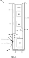
- FIG. 3 is an illustration 300 of a portion of the side view of FIG. 2 , enlarged for clarity.
- Each of the plurality of sides 114, 116, 120 of the housing 106 includes an interior surface 302 facing the internal components 202, 204 and an exterior surface 304.
- a finger is shown touching the exterior surface 304 of the top side 116 of the housing 106.
- a touch temperature (T T ) at the finger and a surface temperature (T S ) at the exterior surface 304 experience a transient thermal response, during which the respective temperatures T T and T S converge to a common temperature referred to as a contact temperature (T C ).
- T T touch temperature
- T S surface temperature
- FIG. 4 is a graph of an example transient thermal response when a finger touches an external surface of a device.
- the graph shows that upon contact between the finger and the surface, the surface temperature of the device decreases rapidly while the touch temperature increases quickly. After touching for 3 seconds, the surface temperature and the touch temperature obtain a thermal steady state condition and converge to a contact temperature.
- a porous and thermally conductive material 306, 308, 310 is associated with at least one of the plurality of sides 114, 116, 120 of the housing 106.
- the porous and thermally conductive material 306, 308, 310 is designed to have properties, e.g., thermal conductivity (k), a density (p), and a specific heat (C p ), that maintain a surface temperature (T S ) at the exterior surface 304 of the at least one side 114, 116, 120 of the housing 106 in a range between 30C and 60C, or in a range between 36C and 45C, or at or near average human body temperature (e.g., 37.5C), during a steady state operation of the device.
- properties e.g., thermal conductivity (k), a density (p), and a specific heat (C p ), that maintain a surface temperature (T S ) at the exterior surface 304 of the at least one side 114, 116, 120 of the housing 106 in a range between 30C and
- a material having an intrinsic thermal conductivity (k) may be designed and made to have a porosity that results in a porous and thermally conductive skin material having a density (p) and a specific heat (C p ) such that the product k ⁇ ⁇ ⁇ C p for the skin material is between 0 (J ⁇ W)/(m 4 ⁇ K 2 ) and 1,000,000 (J ⁇ W)/(m 4 ⁇ K 2 ).
- the variables are: joules (J), watts (W), meters (m) and Kelvin (K).
- human skin has a thermal conductivity (k) of approximately 0.23 W/m-K, a density (p) of approximately 1200 kg/m 3 and a specific heat (C p ) of approximately 3590 J/kg-K.
- the variables are: joules (J), watts (W), meters (m), kilogram (kg), and Kelvin (K).
- the product k ⁇ ⁇ ⁇ C p for human skin is thus approximately 990,000 (J ⁇ W)/(m 4 ⁇ K 2 ).
- the skin material is designed to have a product k ⁇ ⁇ ⁇ C p that is around or less than the product k ⁇ ⁇ ⁇ C p for human skin, e.g., between 0 (J ⁇ W)/(m 4 ⁇ K 2 ) and 1,000,000 (J ⁇ W)/(m 4 ⁇ K 2 ).
- Maintaining the surface temperature (T S ) at the exterior surface 304 within these temperature ranges ensures that the transient thermal response (such as shown in FIG. 4 ) between a user and the device will result in a contact temperature T C within these same temperature range of 30C and 60C.
- Steady state operation in this context means that the device is operating under normal operation and environmental conditions. In other words, the device is not experiencing any operation abnormalities that are causing internal components to overheat, and the device is not exposed to a high ambient temperature, e.g., direct sunlight in a high temperature environment.
- the porous and thermally conductive material associated with the sides of the housing is a layer 306 of material on one or both of the interior surface and exterior surface of the side 120.
- the layer 306 of material may have a thickness in the range of 100 microns and 1.00 mm.
- the material may be associated with all sides of the housing 106 to thereby provide a device with a housing that is entirely coated, either internally, externally, or both internally and externally, with the material.
- the porous and thermally conductive material 308 associated with the sides of the housing 106 forms the entire side 114 of the housing.
- the side of material may have a thickness in the range of 50 ⁇ m to 100mm.
- the material 308 may form all sides of the housing 106 to thereby provide a device with a housing that is formed entirely of the material.
- the porous and thermally conductive material 306, 308, 310 associated with the sides of the housing may be a metal, a glass, a plastic, e.g., polyethylene, or a combined metal/plastic material.
- the entire top side 116 of the housing 106, or at least the display portion 118 of the top side may be formed of porous glass 310; while the first side 108, second side 110, third side 112, fourth side 114 and bottom side 120 of the housing may be formed of a porous metal 308, such as porous aluminum, or a porous plastic, such as porous polyethylene.
- a glass-based skin material may have a thermal conductivity (k) between 0.5 - 2 W/m-K, a density ( ⁇ ) between 1000 - 2500 kg/m 3 , and a specific heat (C p ) between 500 - 1000 J/kg-K.
- the glass-based skin material may be designed and made to have a porosity that results in a glass-based skin material having a density ( ⁇ ) and a specific heat (C p ) such that the product k ⁇ ⁇ ⁇ C p for the end glass-based skin material is between 0 (J ⁇ W)/(m 4 ⁇ K 2 ) and 1,000,000 (J ⁇ W)/(m 4 ⁇ K 2 ).
- This combination of properties of a glass-based skin material may be obtained by structuring the material to have a porosity between 10% and 70%.
- the material may have a porosity between 30% and 50%, and may be fabricated using material particles sized between 100 and 200 ⁇ m.
- a glass-based skin material 310 may be associated with the top side 116 of the housing 106.
- the glass-based skin material 310 may be used to form the display portion 118 of the top side 116 of the housing 106.
- the glass-based skin material 310 may be used to form the entire top side 116 including the display portion 118.
- the top side or the display portion may be formed using well known techniques, such as sintering.
- the glass-based skin material may be applied as a layer on the entire top side 116 or at least on the display portion 118 of the top side. The layer may be applied to the side using well known techniques, such as compression molding.
- a metal-based skin material may have a thermal conductivity between 300 - 400 W/m-K, a density between 4000-8000 kg/m 3 , and a specific heat between 200 - 300 J/kg-K.
- the metal-based skin material may be designed and made to have a porosity that results in a metal-based skin material having a density (p) and a specific heat (C p ) such that the product k ⁇ ⁇ ⁇ C p for the end metal-based skin material is between 0 (J ⁇ W)/(m 4 ⁇ K 2 ) and 1,000,000 (J ⁇ W)/(m 4 ⁇ K 2 ).
- This combination of material properties of a metal-based skin material may be obtained by structuring the material to have a porosity between 10% and 70%.
- the material may have a porosity between 30% and 50%, and may be fabricated using material particles sized between 100 and 200 ⁇ m.
- a plastic-based material may have a thermal conductivity may between 0.1 - 0.4 W/m-K, a density between 900 - 1000 kg/m 3 , and a specific heat between 1900 - 2000 J/kg-K.
- the plastic-based skin material may be designed and made to have a porosity that results in a plastic-based skin material having a density (p) and a specific heat (C p ) such that the product k ⁇ ⁇ ⁇ C p for the end metal-based skin material is between 0 (J ⁇ W)/(m 4 ⁇ K 2 ) and 1,000,000 (J ⁇ W)/(m 4 ⁇ K 2 ).
- This combination of material properties of a plastic-based material may be obtained by structuring the material to have a porosity between 10% and 70%.
- the material may have a porosity between 30% and 50%, and may be fabricated using material particles sized between 100 and 200 ⁇ m.
- a metal-based, plastic-based, or combined metal/plastic-based skin material may be associated with first side 108, second side 110, third side 112, fourth side 114, and bottom side 120 of the housing.
- a metal-based, plastic-based or combined metal/plastic-based skin material may applied as a layer 306 on the bottom side 120, or the material 308 may be used to form one or more sides, such as the fourth side 114.
- junction temperatures T J
- the skin material of the device is further configured to have a density, thermal conductivity, and specific heat that maintain these junction temperatures below a threshold level. For example, if the electronic device has a number of electronic components 202, 204 and each component is able to operate in or at a temperature not exceeding 100C, then the material may be configured to maintain the junction temperature below 100C.
- example skin materials designed to achieve the forgoing include a porous polyethylene, having a smooth surface of between 30-50 microns, a thickness of 1.00mm, a porosity of 40-50% and a particle size of approximately 100um (referred to as "material A"), and a porous polyethylene, having a coarse surface of between 100-200 microns, a thickness of 1.00mm, a porosity of 40-50% and a particle size of approximately 100um (referred to as "material B").
- Each of material A and material B has a thermal conductivity (k) between 0.1 - 0.15 W/m-K, a density(p) of about 470 kg/m 3 , and a specific heat (C p ) of about 950 W/m-K. Based on these material properties, the product k ⁇ ⁇ ⁇ C p for materials A and B may be between 44,650 (J ⁇ W)/(m 4 ⁇ K 2 ) and 66,975 (J ⁇ W)/(m 4 ⁇ K 2 ).
- the surface texture may be adjusted by surface grinding/polishing to obtain a desired smoothness.
- Surface texture may also be controlled by the particle size used to form the skin.
- the same particle size was used for material A and material B.
- Material A was provided with a smooth surface of between 30-50 microns through surface grinding/polishing.
- Material A provided a junction temperature of 97C and a surface temperature of 47.3C, while the conventional material provided a junction temperature of 90C and a surface temperature of 53.8C. In this case, when compared to the conventional material, material A reduced the surface temperature by 7C. Although the junction temperature increased by 6.5C relative to the conventional material, the increase did not result in a junction temperature that exceeded acceptable operating conditions.
- Material B provided a junction temperature of 98C and a surface temperature of 46C, while the conventional material provided a junction temperature of 89C and a surface temperature of 53.9C.
- material A reduced the surface temperature by 7.9C.
- the junction temperature increased by 9C relative to the conventional material, the increase did not result in a junction temperature that exceeded acceptable operating conditions.
- an electronic device 100 that include a housing 106 defined by a plurality of sides 108. 110, 112, 114, 120, and electronics components 202, 204, 206 contained in the housing.
- a porous and thermally conductive material 306, 308, 310 may be associated with at least one of the plurality of sides of the housing 106.
- the material 306, 308, 310 has a thermal conductively (k), and a porosity of between 10% and 70% that results in a specific heat (p) and density (C p ) for the material, such that a product k ⁇ ⁇ ⁇ C p is between 0 (J ⁇ W)/(m 4 ⁇ K 2 ) and 1,000,000 (J ⁇ W)/(m 4 ⁇ K 2 ).
- the material 306, 308, 310 may comprise one of: a glass-based material having a thermal conductivity between 0.5 - 2 W/m-K, a density between 1000 - 2500 kg/m 3 , and a specific heat between 500 - 1000 J/kg-K; a metal-based material having a thermal conductivity between 300 - 400 W/m-K, a density between 4000 - 8000 kg/m 3 , and a specific heat between 200 - 300 J/kg-K; and a plastic-based material having a thermal conductivity may be between 0.1 - 0.4 W/m-K, a density between 400 - 1000 kg/m 3 , and a specific heat between 1900 - 2000 J/kg-K.
- FIG. 5 is a flow chart 500 of a method of making a housing sub-structure for an electronic device.
- the housing sub-structure may include one or more housing components 108, 110, 112, 114, 116, 120.
- a housing sub-structure may have a first side 108, a second side 110, a third side 112, a fourth side 114 and a bottom side 120.
- the housing sub-structure may be a unitary structure defined by housing components 108, 110, 112, 114, 120 and formed using known manufacturing techniques, such as molding.
- the housing sub-structure may be formed of housing components 108, 110, 112, 114, 120 that are individually fabricated and then assembled to form the housing sub-structure.
- the housing sub-structure may be a single housing component.
- the top side 116 of a housing may define a housing sub-structure.
- a porous and thermally conductive material is obtained.
- the material has a thermal conductively (k) and a porosity of between 10% and 70%, wherein the porosity results in a specific heat (p) and density (C p ) for the material, such that a product k ⁇ ⁇ ⁇ C p is between 0 (J ⁇ W)/(m 4 ⁇ K 2 ) and 1,000,000 (J ⁇ W)/(m 4 ⁇ K 2 ).
- the material may be one of: a glass-based material having a thermal conductivity between 0.5 - 2 W/m-K, a density between 1000 - 2500 kg/m 3 , and a specific heat between 500 - 1000 J/kg-K; a metal-based material having a thermal conductivity between 300 - 400 W/m-K, a density between 4000 - 8000 kg/m 3 , and a specific heat between 200 - 300 J/kg-K; and a plastic-based material having a thermal conductivity may be between 0.1 - 0.4 W/m-K, a density between 400 - 1000 kg/m 3 , and a specific heat between 1900 - 2000 J/kg-K.
- the porous and thermally conductive material is associated with at least one component of the housing sub-structure. Association may occur by applying a layer of the material to the component or through formation of the component using the material. In the case of association, the at least one component may have an interior surface and an exterior surface and associating the material with the at least one component may include applying a layer of the material on one or both of the interior surface and the exterior surface of the component. The thickness of the layer may range between 100 microns and 1.00mm. In the case of forming the housing substructure of the material, the thickness of the at least one component formed of the material may range between 50 ⁇ m and 100mm.
- Fabrication of the foregoing skin materials may be done using known methods, including for example, sintering.
- Sintering technology is used to fabricate porous materials. During sintering processes, material particles are held in a mold and then heated to a temperature below the melting point. The atoms in the particles diffuse across the boundaries of the particles, fusing the particles together and creating one solid piece.
- the porosity of a material can be controlled by particle size. Porosity may be further controlled based on packing density.
- FIG. 6 is a flow chart 600 of a method of operating an electronic device.
- heat is generated in an interior of a housing of the electronic device.
- the housing has a plurality of sides, and each side has an interior surface and an exterior surface.
- the housing of the electronic device may include electronic components and generating heat in the interior of the housing may include dissipating heat from at least one electronic component within the housing.
- the conducting may occur through a porous and thermally conductive material associated with at least one of the plurality of sides of the housing.
- the material has a thermal conductively (k) and a porosity of between 10% and 70%, wherein the porosity results in a specific heat (p) and density (C p ) for the porous and thermally conductive material, such that a product k ⁇ ⁇ ⁇ C p is between 0 (J ⁇ W)/(m 4 ⁇ K 2 ) and 1,000,000 (J ⁇ W)/(m 4 ⁇ K 2 ).
- the porosity of the porous and thermally conductive material is between 30% and 50%.
- the porous and thermally conductive material may be one of: a glass-based material having a thermal conductivity between 0.5 - 2 W/m-K, a density between 1000 - 2500 kg/m 3 , and a specific heat between 500 - 1000 J/kg-K; a metal-based material having a thermal conductivity between 300 - 400 W/m-K, a density between 4000 - 8000 kg/m 3 , and a specific heat between 200 - 300 J/kg-K; and a plastic-based material having a thermal conductivity may be between 0.1 - 0.4 W/m-K, a density between 400 - 1000 kg/m 3 , and a specific heat between 1900 - 2000 J/kg-K.
- the porous and thermally conductive material may be a layer associated with one or both of the interior surface and the exterior surface of the at least one of the plurality of sides of the housing.
- the porous and thermally conductive material may form the at least one of the plurality of sides.
- the porous and thermally conductive material may form an entirety of the housing.
- the heat generated in the interior of the housing creates a junction temperature at the interior surface of the at least one side of the housing, and conducting at least a portion of the heat generated in the interior of the housing includes maintaining a surface temperature at the exterior surface of the at least one side in a range between 30C and 60C during a steady state operation of the electronic device, and maintaining the junction temperature below a threshold level.
- FIG. 7 is an illustration 700 of a side view, with interior components exposed, of an electronic device 702 configured in accordance with aspects disclosed herein to implement the method of FIG. 6 .
- the electronic device 702 may include means for generating heat in an interior 722 of a housing 704 of the electronic device.
- the housing 704 may have a plurality of sides 706, 708, 710, 712, each having an interior surface 714 and an exterior surface 716.
- the means for generating heat in the interior 722 of the housing 704 may include one or more electronic components 718 within the housing that are configured to dissipate heat.
- the electronic device 702 may further include means for conducting at least a portion of the heat generated in the interior 722 of the housing 704 to an environment exterior the housing.
- the means for conducting may comprise a porous and thermally conductive material 720 associated with at least one of the plurality of sides 706, 708, 710, 712 of the housing 704.
- the material 720 may have a thermal conductively (k) and a porosity of between 10% and 70%, wherein the porosity results in a specific heat (p) and density (C p ) for the porous and thermally conductive material, such that a product k ⁇ ⁇ ⁇ C p is between 0 (J ⁇ W)/(m 4 ⁇ K 2 ) and 1,000,000 (J ⁇ W)/(m 4 ⁇ K 2 ).
- the porosity of the porous and thermally conductive material 720 may be between 30% and 50%.
- the porous and thermally conductive material 720 may be a layer associated with one or both of the interior surface and the exterior surface of the at least one of the plurality of sides 706, 708, 710, 712 of the housing 704. In another configuration, the porous and thermally conductive material 720 may form the at least one of the plurality of sides706, 708, 710, 712 of the housing 704. In yet another configuration, the porous and thermally conductive material 720 may form an entirety of the housing 704.
- the porous and thermally conductive material 720 may be at least one of: a glass-based material having a thermal conductivity between 0.5 - 2 W/m-K, a density between 1000 - 2500 kg/m 3 , and a specific heat between 500 - 1000 J/kg-K; a metal-based material having a thermal conductivity between 300 - 400 W/m-K, a density between 4000 - 8000 kg/m 3 , and a specific heat between 200 - 300 J/kg-K; and a plastic-based material having a thermal conductivity may be between 0.1 - 0.4 W/m-K, a density between 400 - 1000 kg/m 3 , and a specific heat between 1900 - 2000 J/kg-K.
- the heat generated by the means for generating heat in the interior 722 of the housing 704 creates a junction temperature at the interior surface 714 of the at least one of the plurality of sides 706, 708, 710, 712.
- the means for conducting at least a portion of the heat generated in the interior 714 of the housing 704 is configured to maintain a surface temperature at the exterior surface 716 of the at least one of the plurality of sides 706, 708, 710, 712 of the housing in a range between 30C and 60C during a steady state operation of the electronic device, and to maintain the junction temperature below a threshold level.
- Combinations such as "at least one of A, B, or C,” “at least one of A, B, and C,” and “A, B, C, or any combination thereof' include any combination of A, B, and/or C, and may include multiples of A, multiples of B, or multiples of C.
- combinations such as “at least one of A, B, or C,” “at least one of A, B, and C,” and “A, B, C, or any combination thereof' may be A only, B only, C only, A and B, A and C, B and C, or A and B and C, where any such combinations may contain one or more member or members of A, B, or C.
Landscapes
- Engineering & Computer Science (AREA)
- Theoretical Computer Science (AREA)
- Physics & Mathematics (AREA)
- General Engineering & Computer Science (AREA)
- Human Computer Interaction (AREA)
- General Physics & Mathematics (AREA)
- Computer Hardware Design (AREA)
- Chemical & Material Sciences (AREA)
- Thermal Sciences (AREA)
- Electromagnetism (AREA)
- Power Engineering (AREA)
- Chemical Kinetics & Catalysis (AREA)
- Combustion & Propulsion (AREA)
- Materials Engineering (AREA)
- Organic Chemistry (AREA)
- Dispersion Chemistry (AREA)
- Mechanical Engineering (AREA)
- Casings For Electric Apparatus (AREA)
- Cooling Or The Like Of Electrical Apparatus (AREA)
- Laminated Bodies (AREA)
- Microelectronics & Electronic Packaging (AREA)
Applications Claiming Priority (3)
| Application Number | Priority Date | Filing Date | Title |
|---|---|---|---|
| US201461953653P | 2014-03-14 | 2014-03-14 | |
| US14/594,984 US10152099B2 (en) | 2014-03-14 | 2015-01-12 | Skin material design to reduce touch temperature |
| PCT/US2015/020559 WO2015138973A1 (en) | 2014-03-14 | 2015-03-13 | Skin material design to reduce touch temperature |
Publications (2)
| Publication Number | Publication Date |
|---|---|
| EP3117174A1 EP3117174A1 (en) | 2017-01-18 |
| EP3117174B1 true EP3117174B1 (en) | 2019-09-18 |
Family
ID=54068815
Family Applications (1)
| Application Number | Title | Priority Date | Filing Date |
|---|---|---|---|
| EP15718646.1A Active EP3117174B1 (en) | 2014-03-14 | 2015-03-13 | Skin material design to reduce touch temperature |
Country Status (6)
| Country | Link |
|---|---|
| US (1) | US10152099B2 (OSRAM) |
| EP (1) | EP3117174B1 (OSRAM) |
| JP (1) | JP2017513214A (OSRAM) |
| KR (1) | KR20160132388A (OSRAM) |
| CN (1) | CN106133634B (OSRAM) |
| WO (1) | WO2015138973A1 (OSRAM) |
Families Citing this family (5)
| Publication number | Priority date | Publication date | Assignee | Title |
|---|---|---|---|---|
| US12114453B2 (en) * | 2019-01-29 | 2024-10-08 | Apple Inc. | Core shell with various filler materials for enhanced thermal conductivity |
| US11379023B2 (en) * | 2019-07-15 | 2022-07-05 | Microsoft Technology Licensing, Llc | Regulating device surface temperature |
| US12070797B1 (en) | 2020-05-20 | 2024-08-27 | Apple Inc. | Direct metal deposition of electronic device components |
| CN119663395A (zh) | 2020-05-20 | 2025-03-21 | 苹果公司 | 非水性铝阳极化 |
| US11716808B2 (en) * | 2020-12-10 | 2023-08-01 | International Business Machines Corporation | Tamper-respondent assemblies with porous heat transfer element(s) |
Family Cites Families (9)
| Publication number | Priority date | Publication date | Assignee | Title |
|---|---|---|---|---|
| JP2006114736A (ja) * | 2004-10-15 | 2006-04-27 | Sumitomo Chemical Co Ltd | 携帯電子機器 |
| US7695808B2 (en) * | 2005-11-07 | 2010-04-13 | 3M Innovative Properties Company | Thermal transfer coating |
| US7355849B2 (en) * | 2006-01-09 | 2008-04-08 | Via Technologies, Inc. Of R.O.C. | Non-metal mesh cover for metal chassis |
| US20070263352A1 (en) * | 2006-05-15 | 2007-11-15 | Motorola, Inc. | Plastics Utilizing Thermally Conductive Film |
| JP2008277432A (ja) * | 2007-04-26 | 2008-11-13 | Kaneka Corp | 放熱構造体 |
| JP2010251463A (ja) * | 2009-04-14 | 2010-11-04 | Asahi Kasei E-Materials Corp | 新規吸熱シート |
| US8800641B2 (en) | 2009-06-01 | 2014-08-12 | The Boeing Company | Methods and apparatus for a micro-truss based structural insulation layer |
| US20150005043A1 (en) * | 2012-01-16 | 2015-01-01 | Nec Casio Modile Communications, Ltd. | Portable terminal device |
| US9165854B2 (en) * | 2012-04-12 | 2015-10-20 | Qualcomm Incorporated | Heat dissipation features, electronic devices incorporating heat dissipation features, and methods of making heat dissipation features |
-
2015
- 2015-01-12 US US14/594,984 patent/US10152099B2/en active Active
- 2015-03-13 JP JP2016555573A patent/JP2017513214A/ja active Pending
- 2015-03-13 CN CN201580013484.6A patent/CN106133634B/zh not_active Expired - Fee Related
- 2015-03-13 KR KR1020167024234A patent/KR20160132388A/ko not_active Withdrawn
- 2015-03-13 WO PCT/US2015/020559 patent/WO2015138973A1/en not_active Ceased
- 2015-03-13 EP EP15718646.1A patent/EP3117174B1/en active Active
Non-Patent Citations (1)
| Title |
|---|
| None * |
Also Published As
| Publication number | Publication date |
|---|---|
| EP3117174A1 (en) | 2017-01-18 |
| US10152099B2 (en) | 2018-12-11 |
| WO2015138973A1 (en) | 2015-09-17 |
| US20150261267A1 (en) | 2015-09-17 |
| CN106133634B (zh) | 2019-11-29 |
| JP2017513214A (ja) | 2017-05-25 |
| CN106133634A (zh) | 2016-11-16 |
| KR20160132388A (ko) | 2016-11-18 |
Similar Documents
| Publication | Publication Date | Title |
|---|---|---|
| EP3117174B1 (en) | Skin material design to reduce touch temperature | |
| Hong et al. | Wearable thermoelectrics for personalized thermoregulation | |
| US9165854B2 (en) | Heat dissipation features, electronic devices incorporating heat dissipation features, and methods of making heat dissipation features | |
| US8872997B2 (en) | Display assembly | |
| US20160266629A1 (en) | Changing power limits based on device state | |
| US20160266628A1 (en) | Power management to change power limits based on device skin temperature | |
| KR102709687B1 (ko) | 방열 구조 및 그를 포함하는 전자 장치 | |
| CN101529359A (zh) | 薄的被动冷却系统 | |
| JP3242612U (ja) | 充電装置 | |
| JP2014220371A (ja) | 放熱部材および電子機器 | |
| US20050280987A1 (en) | Phase change materials as a heat sink for computers | |
| CN107734946B (zh) | 运载工具电池中印刷电路板散热方法、装置、计算机可读存储介质以及运载工具电池 | |
| US10041894B1 (en) | Thermal conductivity measurement of anisotropic substrates | |
| US9425374B2 (en) | Electronic apparatus and protective cover of mobile device | |
| CN105700649A (zh) | 散热系统及电子设备 | |
| US10504812B1 (en) | Heating-cooling module | |
| US8363398B2 (en) | Electronic device with heat dissipation casing | |
| CN203633035U (zh) | 散热结构和电子设备 | |
| JP2017162857A (ja) | ヒートシンクシート及び携帯用情報機器 | |
| CN206525067U (zh) | 可携带电子装置的复合支撑散热结构 | |
| JP2007250725A (ja) | 携帯端末装置 | |
| CN214627766U (zh) | 散热结构和电子设备 | |
| US20250246501A1 (en) | Integrated circuit assembly with die coupled to lid | |
| TWM505630U (zh) | 穿戴式電子裝置 | |
| US20220129039A1 (en) | Electronic device housings with shock absorbers |
Legal Events
| Date | Code | Title | Description |
|---|---|---|---|
| STAA | Information on the status of an ep patent application or granted ep patent |
Free format text: STATUS: THE INTERNATIONAL PUBLICATION HAS BEEN MADE |
|
| PUAI | Public reference made under article 153(3) epc to a published international application that has entered the european phase |
Free format text: ORIGINAL CODE: 0009012 |
|
| STAA | Information on the status of an ep patent application or granted ep patent |
Free format text: STATUS: REQUEST FOR EXAMINATION WAS MADE |
|
| 17P | Request for examination filed |
Effective date: 20160819 |
|
| AK | Designated contracting states |
Kind code of ref document: A1 Designated state(s): AL AT BE BG CH CY CZ DE DK EE ES FI FR GB GR HR HU IE IS IT LI LT LU LV MC MK MT NL NO PL PT RO RS SE SI SK SM TR |
|
| AX | Request for extension of the european patent |
Extension state: BA ME |
|
| DAV | Request for validation of the european patent (deleted) | ||
| DAX | Request for extension of the european patent (deleted) | ||
| STAA | Information on the status of an ep patent application or granted ep patent |
Free format text: STATUS: EXAMINATION IS IN PROGRESS |
|
| 17Q | First examination report despatched |
Effective date: 20180620 |
|
| GRAP | Despatch of communication of intention to grant a patent |
Free format text: ORIGINAL CODE: EPIDOSNIGR1 |
|
| STAA | Information on the status of an ep patent application or granted ep patent |
Free format text: STATUS: GRANT OF PATENT IS INTENDED |
|
| INTG | Intention to grant announced |
Effective date: 20190328 |
|
| GRAS | Grant fee paid |
Free format text: ORIGINAL CODE: EPIDOSNIGR3 |
|
| GRAA | (expected) grant |
Free format text: ORIGINAL CODE: 0009210 |
|
| STAA | Information on the status of an ep patent application or granted ep patent |
Free format text: STATUS: THE PATENT HAS BEEN GRANTED |
|
| AK | Designated contracting states |
Kind code of ref document: B1 Designated state(s): AL AT BE BG CH CY CZ DE DK EE ES FI FR GB GR HR HU IE IS IT LI LT LU LV MC MK MT NL NO PL PT RO RS SE SI SK SM TR |
|
| REG | Reference to a national code |
Ref country code: GB Ref legal event code: FG4D |
|
| REG | Reference to a national code |
Ref country code: CH Ref legal event code: EP |
|
| REG | Reference to a national code |
Ref country code: DE Ref legal event code: R096 Ref document number: 602015038192 Country of ref document: DE |
|
| REG | Reference to a national code |
Ref country code: AT Ref legal event code: REF Ref document number: 1181842 Country of ref document: AT Kind code of ref document: T Effective date: 20191015 |
|
| REG | Reference to a national code |
Ref country code: IE Ref legal event code: FG4D |
|
| REG | Reference to a national code |
Ref country code: NL Ref legal event code: MP Effective date: 20190918 |
|
| PG25 | Lapsed in a contracting state [announced via postgrant information from national office to epo] |
Ref country code: NO Free format text: LAPSE BECAUSE OF FAILURE TO SUBMIT A TRANSLATION OF THE DESCRIPTION OR TO PAY THE FEE WITHIN THE PRESCRIBED TIME-LIMIT Effective date: 20191218 Ref country code: HR Free format text: LAPSE BECAUSE OF FAILURE TO SUBMIT A TRANSLATION OF THE DESCRIPTION OR TO PAY THE FEE WITHIN THE PRESCRIBED TIME-LIMIT Effective date: 20190918 Ref country code: SE Free format text: LAPSE BECAUSE OF FAILURE TO SUBMIT A TRANSLATION OF THE DESCRIPTION OR TO PAY THE FEE WITHIN THE PRESCRIBED TIME-LIMIT Effective date: 20190918 Ref country code: FI Free format text: LAPSE BECAUSE OF FAILURE TO SUBMIT A TRANSLATION OF THE DESCRIPTION OR TO PAY THE FEE WITHIN THE PRESCRIBED TIME-LIMIT Effective date: 20190918 Ref country code: LT Free format text: LAPSE BECAUSE OF FAILURE TO SUBMIT A TRANSLATION OF THE DESCRIPTION OR TO PAY THE FEE WITHIN THE PRESCRIBED TIME-LIMIT Effective date: 20190918 Ref country code: BG Free format text: LAPSE BECAUSE OF FAILURE TO SUBMIT A TRANSLATION OF THE DESCRIPTION OR TO PAY THE FEE WITHIN THE PRESCRIBED TIME-LIMIT Effective date: 20191218 |
|
| REG | Reference to a national code |
Ref country code: LT Ref legal event code: MG4D |
|
| PG25 | Lapsed in a contracting state [announced via postgrant information from national office to epo] |
Ref country code: GR Free format text: LAPSE BECAUSE OF FAILURE TO SUBMIT A TRANSLATION OF THE DESCRIPTION OR TO PAY THE FEE WITHIN THE PRESCRIBED TIME-LIMIT Effective date: 20191219 Ref country code: LV Free format text: LAPSE BECAUSE OF FAILURE TO SUBMIT A TRANSLATION OF THE DESCRIPTION OR TO PAY THE FEE WITHIN THE PRESCRIBED TIME-LIMIT Effective date: 20190918 Ref country code: AL Free format text: LAPSE BECAUSE OF FAILURE TO SUBMIT A TRANSLATION OF THE DESCRIPTION OR TO PAY THE FEE WITHIN THE PRESCRIBED TIME-LIMIT Effective date: 20190918 Ref country code: RS Free format text: LAPSE BECAUSE OF FAILURE TO SUBMIT A TRANSLATION OF THE DESCRIPTION OR TO PAY THE FEE WITHIN THE PRESCRIBED TIME-LIMIT Effective date: 20190918 |
|
| REG | Reference to a national code |
Ref country code: AT Ref legal event code: MK05 Ref document number: 1181842 Country of ref document: AT Kind code of ref document: T Effective date: 20190918 |
|
| PG25 | Lapsed in a contracting state [announced via postgrant information from national office to epo] |
Ref country code: RO Free format text: LAPSE BECAUSE OF FAILURE TO SUBMIT A TRANSLATION OF THE DESCRIPTION OR TO PAY THE FEE WITHIN THE PRESCRIBED TIME-LIMIT Effective date: 20190918 Ref country code: NL Free format text: LAPSE BECAUSE OF FAILURE TO SUBMIT A TRANSLATION OF THE DESCRIPTION OR TO PAY THE FEE WITHIN THE PRESCRIBED TIME-LIMIT Effective date: 20190918 Ref country code: ES Free format text: LAPSE BECAUSE OF FAILURE TO SUBMIT A TRANSLATION OF THE DESCRIPTION OR TO PAY THE FEE WITHIN THE PRESCRIBED TIME-LIMIT Effective date: 20190918 Ref country code: PL Free format text: LAPSE BECAUSE OF FAILURE TO SUBMIT A TRANSLATION OF THE DESCRIPTION OR TO PAY THE FEE WITHIN THE PRESCRIBED TIME-LIMIT Effective date: 20190918 Ref country code: EE Free format text: LAPSE BECAUSE OF FAILURE TO SUBMIT A TRANSLATION OF THE DESCRIPTION OR TO PAY THE FEE WITHIN THE PRESCRIBED TIME-LIMIT Effective date: 20190918 Ref country code: IT Free format text: LAPSE BECAUSE OF FAILURE TO SUBMIT A TRANSLATION OF THE DESCRIPTION OR TO PAY THE FEE WITHIN THE PRESCRIBED TIME-LIMIT Effective date: 20190918 Ref country code: AT Free format text: LAPSE BECAUSE OF FAILURE TO SUBMIT A TRANSLATION OF THE DESCRIPTION OR TO PAY THE FEE WITHIN THE PRESCRIBED TIME-LIMIT Effective date: 20190918 Ref country code: PT Free format text: LAPSE BECAUSE OF FAILURE TO SUBMIT A TRANSLATION OF THE DESCRIPTION OR TO PAY THE FEE WITHIN THE PRESCRIBED TIME-LIMIT Effective date: 20200120 |
|
| PGFP | Annual fee paid to national office [announced via postgrant information from national office to epo] |
Ref country code: GB Payment date: 20200103 Year of fee payment: 6 Ref country code: DE Payment date: 20200113 Year of fee payment: 6 |
|
| PG25 | Lapsed in a contracting state [announced via postgrant information from national office to epo] |
Ref country code: IS Free format text: LAPSE BECAUSE OF FAILURE TO SUBMIT A TRANSLATION OF THE DESCRIPTION OR TO PAY THE FEE WITHIN THE PRESCRIBED TIME-LIMIT Effective date: 20200224 Ref country code: SM Free format text: LAPSE BECAUSE OF FAILURE TO SUBMIT A TRANSLATION OF THE DESCRIPTION OR TO PAY THE FEE WITHIN THE PRESCRIBED TIME-LIMIT Effective date: 20190918 Ref country code: SK Free format text: LAPSE BECAUSE OF FAILURE TO SUBMIT A TRANSLATION OF THE DESCRIPTION OR TO PAY THE FEE WITHIN THE PRESCRIBED TIME-LIMIT Effective date: 20190918 Ref country code: CZ Free format text: LAPSE BECAUSE OF FAILURE TO SUBMIT A TRANSLATION OF THE DESCRIPTION OR TO PAY THE FEE WITHIN THE PRESCRIBED TIME-LIMIT Effective date: 20190918 |
|
| REG | Reference to a national code |
Ref country code: DE Ref legal event code: R097 Ref document number: 602015038192 Country of ref document: DE |
|
| PGFP | Annual fee paid to national office [announced via postgrant information from national office to epo] |
Ref country code: FR Payment date: 20200106 Year of fee payment: 6 |
|
| PLBE | No opposition filed within time limit |
Free format text: ORIGINAL CODE: 0009261 |
|
| STAA | Information on the status of an ep patent application or granted ep patent |
Free format text: STATUS: NO OPPOSITION FILED WITHIN TIME LIMIT |
|
| PG2D | Information on lapse in contracting state deleted |
Ref country code: IS |
|
| PG25 | Lapsed in a contracting state [announced via postgrant information from national office to epo] |
Ref country code: DK Free format text: LAPSE BECAUSE OF FAILURE TO SUBMIT A TRANSLATION OF THE DESCRIPTION OR TO PAY THE FEE WITHIN THE PRESCRIBED TIME-LIMIT Effective date: 20190918 Ref country code: IS Free format text: LAPSE BECAUSE OF FAILURE TO SUBMIT A TRANSLATION OF THE DESCRIPTION OR TO PAY THE FEE WITHIN THE PRESCRIBED TIME-LIMIT Effective date: 20200119 |
|
| 26N | No opposition filed |
Effective date: 20200619 |
|
| PG25 | Lapsed in a contracting state [announced via postgrant information from national office to epo] |
Ref country code: SI Free format text: LAPSE BECAUSE OF FAILURE TO SUBMIT A TRANSLATION OF THE DESCRIPTION OR TO PAY THE FEE WITHIN THE PRESCRIBED TIME-LIMIT Effective date: 20190918 |
|
| PG25 | Lapsed in a contracting state [announced via postgrant information from national office to epo] |
Ref country code: MC Free format text: LAPSE BECAUSE OF FAILURE TO SUBMIT A TRANSLATION OF THE DESCRIPTION OR TO PAY THE FEE WITHIN THE PRESCRIBED TIME-LIMIT Effective date: 20190918 |
|
| REG | Reference to a national code |
Ref country code: CH Ref legal event code: PL |
|
| REG | Reference to a national code |
Ref country code: BE Ref legal event code: MM Effective date: 20200331 |
|
| PG25 | Lapsed in a contracting state [announced via postgrant information from national office to epo] |
Ref country code: LU Free format text: LAPSE BECAUSE OF NON-PAYMENT OF DUE FEES Effective date: 20200313 |
|
| PG25 | Lapsed in a contracting state [announced via postgrant information from national office to epo] |
Ref country code: IE Free format text: LAPSE BECAUSE OF NON-PAYMENT OF DUE FEES Effective date: 20200313 Ref country code: CH Free format text: LAPSE BECAUSE OF NON-PAYMENT OF DUE FEES Effective date: 20200331 Ref country code: LI Free format text: LAPSE BECAUSE OF NON-PAYMENT OF DUE FEES Effective date: 20200331 |
|
| PG25 | Lapsed in a contracting state [announced via postgrant information from national office to epo] |
Ref country code: BE Free format text: LAPSE BECAUSE OF NON-PAYMENT OF DUE FEES Effective date: 20200331 |
|
| REG | Reference to a national code |
Ref country code: DE Ref legal event code: R119 Ref document number: 602015038192 Country of ref document: DE |
|
| GBPC | Gb: european patent ceased through non-payment of renewal fee |
Effective date: 20210313 |
|
| PG25 | Lapsed in a contracting state [announced via postgrant information from national office to epo] |
Ref country code: DE Free format text: LAPSE BECAUSE OF NON-PAYMENT OF DUE FEES Effective date: 20211001 Ref country code: FR Free format text: LAPSE BECAUSE OF NON-PAYMENT OF DUE FEES Effective date: 20210331 Ref country code: GB Free format text: LAPSE BECAUSE OF NON-PAYMENT OF DUE FEES Effective date: 20210313 |
|
| PG25 | Lapsed in a contracting state [announced via postgrant information from national office to epo] |
Ref country code: TR Free format text: LAPSE BECAUSE OF FAILURE TO SUBMIT A TRANSLATION OF THE DESCRIPTION OR TO PAY THE FEE WITHIN THE PRESCRIBED TIME-LIMIT Effective date: 20190918 Ref country code: MT Free format text: LAPSE BECAUSE OF FAILURE TO SUBMIT A TRANSLATION OF THE DESCRIPTION OR TO PAY THE FEE WITHIN THE PRESCRIBED TIME-LIMIT Effective date: 20190918 Ref country code: CY Free format text: LAPSE BECAUSE OF FAILURE TO SUBMIT A TRANSLATION OF THE DESCRIPTION OR TO PAY THE FEE WITHIN THE PRESCRIBED TIME-LIMIT Effective date: 20190918 |
|
| PG25 | Lapsed in a contracting state [announced via postgrant information from national office to epo] |
Ref country code: MK Free format text: LAPSE BECAUSE OF FAILURE TO SUBMIT A TRANSLATION OF THE DESCRIPTION OR TO PAY THE FEE WITHIN THE PRESCRIBED TIME-LIMIT Effective date: 20190918 |