EP3113163A1 - Device and method for sensing threshold voltage of driving tft included in organic light emitting display - Google Patents
Device and method for sensing threshold voltage of driving tft included in organic light emitting display Download PDFInfo
- Publication number
- EP3113163A1 EP3113163A1 EP16176788.4A EP16176788A EP3113163A1 EP 3113163 A1 EP3113163 A1 EP 3113163A1 EP 16176788 A EP16176788 A EP 16176788A EP 3113163 A1 EP3113163 A1 EP 3113163A1
- Authority
- EP
- European Patent Office
- Prior art keywords
- sensing
- driving tft
- period
- voltage
- during
- Prior art date
- Legal status (The legal status is an assumption and is not a legal conclusion. Google has not performed a legal analysis and makes no representation as to the accuracy of the status listed.)
- Granted
Links
Images






Classifications
-
- G—PHYSICS
- G09—EDUCATION; CRYPTOGRAPHY; DISPLAY; ADVERTISING; SEALS
- G09G—ARRANGEMENTS OR CIRCUITS FOR CONTROL OF INDICATING DEVICES USING STATIC MEANS TO PRESENT VARIABLE INFORMATION
- G09G3/00—Control arrangements or circuits, of interest only in connection with visual indicators other than cathode-ray tubes
- G09G3/20—Control arrangements or circuits, of interest only in connection with visual indicators other than cathode-ray tubes for presentation of an assembly of a number of characters, e.g. a page, by composing the assembly by combination of individual elements arranged in a matrix no fixed position being assigned to or needed to be assigned to the individual characters or partial characters
- G09G3/22—Control arrangements or circuits, of interest only in connection with visual indicators other than cathode-ray tubes for presentation of an assembly of a number of characters, e.g. a page, by composing the assembly by combination of individual elements arranged in a matrix no fixed position being assigned to or needed to be assigned to the individual characters or partial characters using controlled light sources
- G09G3/30—Control arrangements or circuits, of interest only in connection with visual indicators other than cathode-ray tubes for presentation of an assembly of a number of characters, e.g. a page, by composing the assembly by combination of individual elements arranged in a matrix no fixed position being assigned to or needed to be assigned to the individual characters or partial characters using controlled light sources using electroluminescent panels
- G09G3/32—Control arrangements or circuits, of interest only in connection with visual indicators other than cathode-ray tubes for presentation of an assembly of a number of characters, e.g. a page, by composing the assembly by combination of individual elements arranged in a matrix no fixed position being assigned to or needed to be assigned to the individual characters or partial characters using controlled light sources using electroluminescent panels semiconductive, e.g. using light-emitting diodes [LED]
- G09G3/3208—Control arrangements or circuits, of interest only in connection with visual indicators other than cathode-ray tubes for presentation of an assembly of a number of characters, e.g. a page, by composing the assembly by combination of individual elements arranged in a matrix no fixed position being assigned to or needed to be assigned to the individual characters or partial characters using controlled light sources using electroluminescent panels semiconductive, e.g. using light-emitting diodes [LED] organic, e.g. using organic light-emitting diodes [OLED]
- G09G3/3225—Control arrangements or circuits, of interest only in connection with visual indicators other than cathode-ray tubes for presentation of an assembly of a number of characters, e.g. a page, by composing the assembly by combination of individual elements arranged in a matrix no fixed position being assigned to or needed to be assigned to the individual characters or partial characters using controlled light sources using electroluminescent panels semiconductive, e.g. using light-emitting diodes [LED] organic, e.g. using organic light-emitting diodes [OLED] using an active matrix
-
- G—PHYSICS
- G09—EDUCATION; CRYPTOGRAPHY; DISPLAY; ADVERTISING; SEALS
- G09G—ARRANGEMENTS OR CIRCUITS FOR CONTROL OF INDICATING DEVICES USING STATIC MEANS TO PRESENT VARIABLE INFORMATION
- G09G3/00—Control arrangements or circuits, of interest only in connection with visual indicators other than cathode-ray tubes
- G09G3/20—Control arrangements or circuits, of interest only in connection with visual indicators other than cathode-ray tubes for presentation of an assembly of a number of characters, e.g. a page, by composing the assembly by combination of individual elements arranged in a matrix no fixed position being assigned to or needed to be assigned to the individual characters or partial characters
- G09G3/22—Control arrangements or circuits, of interest only in connection with visual indicators other than cathode-ray tubes for presentation of an assembly of a number of characters, e.g. a page, by composing the assembly by combination of individual elements arranged in a matrix no fixed position being assigned to or needed to be assigned to the individual characters or partial characters using controlled light sources
- G09G3/30—Control arrangements or circuits, of interest only in connection with visual indicators other than cathode-ray tubes for presentation of an assembly of a number of characters, e.g. a page, by composing the assembly by combination of individual elements arranged in a matrix no fixed position being assigned to or needed to be assigned to the individual characters or partial characters using controlled light sources using electroluminescent panels
- G09G3/32—Control arrangements or circuits, of interest only in connection with visual indicators other than cathode-ray tubes for presentation of an assembly of a number of characters, e.g. a page, by composing the assembly by combination of individual elements arranged in a matrix no fixed position being assigned to or needed to be assigned to the individual characters or partial characters using controlled light sources using electroluminescent panels semiconductive, e.g. using light-emitting diodes [LED]
- G09G3/3208—Control arrangements or circuits, of interest only in connection with visual indicators other than cathode-ray tubes for presentation of an assembly of a number of characters, e.g. a page, by composing the assembly by combination of individual elements arranged in a matrix no fixed position being assigned to or needed to be assigned to the individual characters or partial characters using controlled light sources using electroluminescent panels semiconductive, e.g. using light-emitting diodes [LED] organic, e.g. using organic light-emitting diodes [OLED]
- G09G3/3225—Control arrangements or circuits, of interest only in connection with visual indicators other than cathode-ray tubes for presentation of an assembly of a number of characters, e.g. a page, by composing the assembly by combination of individual elements arranged in a matrix no fixed position being assigned to or needed to be assigned to the individual characters or partial characters using controlled light sources using electroluminescent panels semiconductive, e.g. using light-emitting diodes [LED] organic, e.g. using organic light-emitting diodes [OLED] using an active matrix
- G09G3/3258—Control arrangements or circuits, of interest only in connection with visual indicators other than cathode-ray tubes for presentation of an assembly of a number of characters, e.g. a page, by composing the assembly by combination of individual elements arranged in a matrix no fixed position being assigned to or needed to be assigned to the individual characters or partial characters using controlled light sources using electroluminescent panels semiconductive, e.g. using light-emitting diodes [LED] organic, e.g. using organic light-emitting diodes [OLED] using an active matrix with pixel circuitry controlling the voltage across the light-emitting element
-
- G—PHYSICS
- G09—EDUCATION; CRYPTOGRAPHY; DISPLAY; ADVERTISING; SEALS
- G09G—ARRANGEMENTS OR CIRCUITS FOR CONTROL OF INDICATING DEVICES USING STATIC MEANS TO PRESENT VARIABLE INFORMATION
- G09G3/00—Control arrangements or circuits, of interest only in connection with visual indicators other than cathode-ray tubes
- G09G3/20—Control arrangements or circuits, of interest only in connection with visual indicators other than cathode-ray tubes for presentation of an assembly of a number of characters, e.g. a page, by composing the assembly by combination of individual elements arranged in a matrix no fixed position being assigned to or needed to be assigned to the individual characters or partial characters
- G09G3/22—Control arrangements or circuits, of interest only in connection with visual indicators other than cathode-ray tubes for presentation of an assembly of a number of characters, e.g. a page, by composing the assembly by combination of individual elements arranged in a matrix no fixed position being assigned to or needed to be assigned to the individual characters or partial characters using controlled light sources
- G09G3/30—Control arrangements or circuits, of interest only in connection with visual indicators other than cathode-ray tubes for presentation of an assembly of a number of characters, e.g. a page, by composing the assembly by combination of individual elements arranged in a matrix no fixed position being assigned to or needed to be assigned to the individual characters or partial characters using controlled light sources using electroluminescent panels
- G09G3/32—Control arrangements or circuits, of interest only in connection with visual indicators other than cathode-ray tubes for presentation of an assembly of a number of characters, e.g. a page, by composing the assembly by combination of individual elements arranged in a matrix no fixed position being assigned to or needed to be assigned to the individual characters or partial characters using controlled light sources using electroluminescent panels semiconductive, e.g. using light-emitting diodes [LED]
- G09G3/3208—Control arrangements or circuits, of interest only in connection with visual indicators other than cathode-ray tubes for presentation of an assembly of a number of characters, e.g. a page, by composing the assembly by combination of individual elements arranged in a matrix no fixed position being assigned to or needed to be assigned to the individual characters or partial characters using controlled light sources using electroluminescent panels semiconductive, e.g. using light-emitting diodes [LED] organic, e.g. using organic light-emitting diodes [OLED]
- G09G3/3225—Control arrangements or circuits, of interest only in connection with visual indicators other than cathode-ray tubes for presentation of an assembly of a number of characters, e.g. a page, by composing the assembly by combination of individual elements arranged in a matrix no fixed position being assigned to or needed to be assigned to the individual characters or partial characters using controlled light sources using electroluminescent panels semiconductive, e.g. using light-emitting diodes [LED] organic, e.g. using organic light-emitting diodes [OLED] using an active matrix
- G09G3/3233—Control arrangements or circuits, of interest only in connection with visual indicators other than cathode-ray tubes for presentation of an assembly of a number of characters, e.g. a page, by composing the assembly by combination of individual elements arranged in a matrix no fixed position being assigned to or needed to be assigned to the individual characters or partial characters using controlled light sources using electroluminescent panels semiconductive, e.g. using light-emitting diodes [LED] organic, e.g. using organic light-emitting diodes [OLED] using an active matrix with pixel circuitry controlling the current through the light-emitting element
-
- G—PHYSICS
- G09—EDUCATION; CRYPTOGRAPHY; DISPLAY; ADVERTISING; SEALS
- G09G—ARRANGEMENTS OR CIRCUITS FOR CONTROL OF INDICATING DEVICES USING STATIC MEANS TO PRESENT VARIABLE INFORMATION
- G09G3/00—Control arrangements or circuits, of interest only in connection with visual indicators other than cathode-ray tubes
- G09G3/20—Control arrangements or circuits, of interest only in connection with visual indicators other than cathode-ray tubes for presentation of an assembly of a number of characters, e.g. a page, by composing the assembly by combination of individual elements arranged in a matrix no fixed position being assigned to or needed to be assigned to the individual characters or partial characters
- G09G3/22—Control arrangements or circuits, of interest only in connection with visual indicators other than cathode-ray tubes for presentation of an assembly of a number of characters, e.g. a page, by composing the assembly by combination of individual elements arranged in a matrix no fixed position being assigned to or needed to be assigned to the individual characters or partial characters using controlled light sources
- G09G3/30—Control arrangements or circuits, of interest only in connection with visual indicators other than cathode-ray tubes for presentation of an assembly of a number of characters, e.g. a page, by composing the assembly by combination of individual elements arranged in a matrix no fixed position being assigned to or needed to be assigned to the individual characters or partial characters using controlled light sources using electroluminescent panels
- G09G3/32—Control arrangements or circuits, of interest only in connection with visual indicators other than cathode-ray tubes for presentation of an assembly of a number of characters, e.g. a page, by composing the assembly by combination of individual elements arranged in a matrix no fixed position being assigned to or needed to be assigned to the individual characters or partial characters using controlled light sources using electroluminescent panels semiconductive, e.g. using light-emitting diodes [LED]
- G09G3/3208—Control arrangements or circuits, of interest only in connection with visual indicators other than cathode-ray tubes for presentation of an assembly of a number of characters, e.g. a page, by composing the assembly by combination of individual elements arranged in a matrix no fixed position being assigned to or needed to be assigned to the individual characters or partial characters using controlled light sources using electroluminescent panels semiconductive, e.g. using light-emitting diodes [LED] organic, e.g. using organic light-emitting diodes [OLED]
- G09G3/3275—Details of drivers for data electrodes
- G09G3/3291—Details of drivers for data electrodes in which the data driver supplies a variable data voltage for setting the current through, or the voltage across, the light-emitting elements
-
- G—PHYSICS
- G09—EDUCATION; CRYPTOGRAPHY; DISPLAY; ADVERTISING; SEALS
- G09G—ARRANGEMENTS OR CIRCUITS FOR CONTROL OF INDICATING DEVICES USING STATIC MEANS TO PRESENT VARIABLE INFORMATION
- G09G2300/00—Aspects of the constitution of display devices
- G09G2300/08—Active matrix structure, i.e. with use of active elements, inclusive of non-linear two terminal elements, in the pixels together with light emitting or modulating elements
- G09G2300/0809—Several active elements per pixel in active matrix panels
- G09G2300/0842—Several active elements per pixel in active matrix panels forming a memory circuit, e.g. a dynamic memory with one capacitor
-
- G—PHYSICS
- G09—EDUCATION; CRYPTOGRAPHY; DISPLAY; ADVERTISING; SEALS
- G09G—ARRANGEMENTS OR CIRCUITS FOR CONTROL OF INDICATING DEVICES USING STATIC MEANS TO PRESENT VARIABLE INFORMATION
- G09G2310/00—Command of the display device
- G09G2310/02—Addressing, scanning or driving the display screen or processing steps related thereto
- G09G2310/0264—Details of driving circuits
- G09G2310/0289—Details of voltage level shifters arranged for use in a driving circuit
-
- G—PHYSICS
- G09—EDUCATION; CRYPTOGRAPHY; DISPLAY; ADVERTISING; SEALS
- G09G—ARRANGEMENTS OR CIRCUITS FOR CONTROL OF INDICATING DEVICES USING STATIC MEANS TO PRESENT VARIABLE INFORMATION
- G09G2320/00—Control of display operating conditions
- G09G2320/02—Improving the quality of display appearance
- G09G2320/0233—Improving the luminance or brightness uniformity across the screen
-
- G—PHYSICS
- G09—EDUCATION; CRYPTOGRAPHY; DISPLAY; ADVERTISING; SEALS
- G09G—ARRANGEMENTS OR CIRCUITS FOR CONTROL OF INDICATING DEVICES USING STATIC MEANS TO PRESENT VARIABLE INFORMATION
- G09G2320/00—Control of display operating conditions
- G09G2320/02—Improving the quality of display appearance
- G09G2320/0252—Improving the response speed
-
- G—PHYSICS
- G09—EDUCATION; CRYPTOGRAPHY; DISPLAY; ADVERTISING; SEALS
- G09G—ARRANGEMENTS OR CIRCUITS FOR CONTROL OF INDICATING DEVICES USING STATIC MEANS TO PRESENT VARIABLE INFORMATION
- G09G2320/00—Control of display operating conditions
- G09G2320/02—Improving the quality of display appearance
- G09G2320/029—Improving the quality of display appearance by monitoring one or more pixels in the display panel, e.g. by monitoring a fixed reference pixel
- G09G2320/0295—Improving the quality of display appearance by monitoring one or more pixels in the display panel, e.g. by monitoring a fixed reference pixel by monitoring each display pixel
-
- G—PHYSICS
- G09—EDUCATION; CRYPTOGRAPHY; DISPLAY; ADVERTISING; SEALS
- G09G—ARRANGEMENTS OR CIRCUITS FOR CONTROL OF INDICATING DEVICES USING STATIC MEANS TO PRESENT VARIABLE INFORMATION
- G09G2320/00—Control of display operating conditions
- G09G2320/04—Maintaining the quality of display appearance
- G09G2320/043—Preventing or counteracting the effects of ageing
Definitions
- the present invention relates to an organic light emitting display, and more particularly, to a device and method for sensing the threshold voltage of a driving TFT included in an organic light emitting display.
- An active-matrix organic light emitting display comprises organic light emitting diodes OLEDs that emit light themselves, and has the advantages of fast response time, high luminous efficiency, high luminance, and wide viewing angle.
- An OLED which is a self-luminous device, comprises an anode and a cathode, and organic compound layers HIL, HTL, EML, ETL, and EIL formed between the anode and cathode.
- the organic compound layers comprise a hole injection layer HIL, a hole transport layer HTL, an emission layer EML, an electron transport layer ETL, and an electron injection layer EIL.
- pixels each comprising an organic light emitting diode are arranged in a matrix, and the luminance of the pixels is adjusted based on the grayscale of video data.
- Each individual pixel comprises a driving TFT (thin-film transistor) that controls the drive current flowing through the OLED.
- the electrical characteristic of the driving TFT such as threshold voltage, mobility, etc., may vary from pixel to pixel because of the process condition, driving environment, etc. Such variation in the electrical characteristics of the driving TFT causes luminance differences between the pixels.
- the technology that senses the characteristic parameters (threshold voltage, mobility, etc.) of the driving TFT of each pixel and corrects image data based on the sensing results is known.
- a driving TFT DT is operated according to a source follower method, and then the source node voltage Vs of the driving TFT DT is detected as a sensing voltage Vsen at the time ta when the gate-source voltage Vgs of the driving TFT DT reaches saturation state by an electric current flowing through the driving TFT DT, in order to sense a change in the threshold voltage Vth of the driving TFT DT.
- a long period of time is needed in order for the gate-source voltage Vgs of the driving TFT DT to reach the threshold voltage Vth of the driving TFT DT. Accordingly, in the conventional art, it is not possible to sense a change in the threshold voltage Vth of the driving TFT DT during real-time operation.
- the present invention is directed to a device and method for sensing the threshold voltage of a driving TFT included in an organic light emitting display so that a change in the threshold voltage of the driving TFT is sensed during real-time operation by reducing sensing time.
- An exemplary embodiment of the present invention provides a device for sensing threshold voltage in an organic light emitting display with a plurality of pixels each having an OLED and a driving TFT for controlling the amount of light emitted by the OLED, the device comprising: a data drive circuit and a timing controller.
- the data drive circuit applies a first data voltage for sensing to the gate node of the driving TFT during a first programming period, obtains the source node voltage of the driving TFT as a first sensing voltage during a first sensing period in which the gate-source voltage of the driving TFT is constantly held at a first value higher than the threshold voltage of the driving TFT, applies a second data voltage for sensing to the gate node of the driving TFT during a second programming period, and obtains the source node voltage of the driving TFT as a second sensing voltage during a second sensing period in which the gate-source voltage of the driving TFT is constantly held at a second value higher than the threshold voltage of the driving TFT.
- the timing controller calculates an nth sensing ratio (n is a positive integer) based on the ratio between the first and second sensing voltages, calculates a change in sensing ratio by comparing the nth sensing ratio with a preset initial sensing ratio, and then obtains a change in the threshold voltage of the driving TFT based on the change in sensing ratio.
- the first programing period and the first sensing period are included in a first compensation period
- the second programming period and the second sensing period are included in a second compensation period.
- the first and second compensation periods are placed in a vertical blanking interval.
- the vertical blanking interval is the time between active intervals for image display
- data for image display is not written during the vertical blanking interval.
- the first and second compensation periods are arranged consecutively in the same vertical blanking interval.
- the first and second compensation periods are placed separately in different vertical blanking intervals.
- the data drive circuit may be adapted to supply a reference voltage to the source node of the driving TFT during a first initial period between the first programming period and the first sensing period.
- the data drive circuit may be adapted to supply the reference voltage to the source node of the driving TFT during a second initial period between the second programming period and the second sensing period.
- a gate drive circuit may be adapted to generate a scan control signal and/or a sensing control signal.
- each pixel may comprise a first switching TFT adapted to be turned on in response to the scan control signal to connect a data line connected to the data drive circuit to the gate node of the driving TFT,
- each pixel may comprise a second switching TFT adapted to be turned on in response to the sensing control signal to connect the source node of the driving TFT to a sensing line connected to a sensing unit in the data drive circuit, and a storage capacitor connected between the gate node and source node of the driving TFT.
- a second switching TFT adapted to be turned on in response to the sensing control signal to connect the source node of the driving TFT to a sensing line connected to a sensing unit in the data drive circuit, and a storage capacitor connected between the gate node and source node of the driving TFT.
- the sensing unit may comprise a reference voltage control switch adapted to be switched on in response to a reference voltage control signal to connect a reference voltage input terminal and the sensing line, and a sampling control switch adapted to be switched on in response to a sampling control signal (SAM) to connect the sensing line and a sample and hold circuit.
- SAM sampling control signal
- the scan control signal is applied at ON level during the first and second programming periods
- the sensing control signal is applied at ON level during the first and second programming periods, the first and second initial periods, and the first and second sensing periods
- the reference voltage control signal is applied at ON level during the first and second programming periods and the first and second initial periods.
- the sampling control signal is applied at ON level during a first sampling period after the first sensing period and a second sampling period after the second sensing period.
- Another exemplary embodiment of the present invention provides a method for sensing threshold voltage in organic light emitting display with a plurality of pixels each having an OLED and a driving TFT for controlling the amount of light emitted by the OLED, the method comprising: applying a first data voltage for sensing to the gate node of the driving TFT during a first programming period and obtaining the source node voltage of the driving TFT as a first sensing voltage during a first sensing period in which the gate-source voltage of the driving TFT is constantly held at a first value higher than the threshold voltage of the driving TFT; applying a second data voltage for sensing to the gate node of the driving TFT during a second programming period and obtaining the source node voltage of the driving TFT as a second sensing voltage during a second sensing period in which the gate-source voltage of the driving TFT is constantly held at a second value higher than the threshold voltage of the driving TFT; and calculating an nth sensing ratio (n is a positive integer) based on the ratio between the first and second
- the first programing period and the first sensing period are included in a first compensation period and the second programming period and the second sensing period are included in a second compensation period.
- the first and second compensation periods are placed in a vertical blanking interval, and the vertical blanking interval is the time between active intervals for image display, wherein data for image display is not written during the vertical blanking interval.
- the first and second compensation periods are placed consecutively in the same vertical blanking interval or the first and second compensation periods are placed separately in different vertical blanking intervals.
- the method may further comprise supplying a reference voltage to the source node of the driving TFT during a first initial period between the first programming period and the first sensing period and supplying the reference voltage to the source node of the driving TFT during a second initial period between the second programming period and the second sensing period.
- FIG. 2 is a view schematically showing an organic light emitting display according to an exemplary embodiment of the present invention.
- FIG. 3 is a view showing an example of the configuration of a pixel array and a data driver IC.
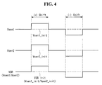
- FIG. 4 is a view showing the principle for deriving a change in the threshold voltage of the driving TFT based on a sensing ratio.
- an organic light emitting display may comprise a display panel 10, a timing controller 11, a data drive circuit 12, a gate drive circuit 13, and a memory 16.
- the gate lines 15 comprise a plurality of first gate lines 15A sequentially supplied with a scan control signal (SCAN of FIG. 5 ) and a plurality of second gate lines 15B sequentially supplied with a sensing control signal (SEN of FIG. 5 ).
- Each pixel P may be connected to any one of the data lines 14A, any one of the sensing lines 14B, any one of the first gate lines 15A, and any one of the second gate lines 15B.
- Each pixel P may be connected to a data line 14A in response to a scan control signal SCAN input through a first gate line 15A, and may be connected to a sensing line 14B in response to a sensing control signal SEN input through a second gate line 15B.
- Each pixel P is supplied with a high-level operating voltage EVDD and a low-level operating voltage EVSS from a power generator (not shown).
- Each pixel P of this invention may comprise an OLED and a driving TFT that drives the OLED.
- the driving TFT may be implemented as p-type or n-type.
- a semiconductor layer of the driving TFT may comprise amorphous silicon, polysilicon, or oxide.
- Each pixel P displays an image, and may operate differently in an image display operation for internally compensating for a change in the mobility of the driving TFT and in a compensation operation for sensing and compensating for a change in the threshold voltage of the driving TFT.
- the compensation operation of this invention may be performed for a predetermined amount of time during power-on or power-off. Particularly, the compensation operation of this invention may reduce the time taken to sense a change in the threshold voltage of the driving TFT by a method to be described later. Thus, it is possible to sense a change in the threshold voltage of the driving TFT during vertical blanking intervals of a real-time operation, that is, image display operation.
- the image display operation and the compensation operation may be implemented depending on the operation of the data drive circuit 12 and gate drive circuit 13 under the control of the timing controller 11.
- the data drive circuit 12 comprises at least one data driver IC (integrated circuit) SDIC.
- the data driver IC may comprise a plurality of digital-to-analog converters (hereinafter, DAC) 121 connected to data lines 14A, a plurality of sensing units 122 connected to sensing lines 14B, a multiplexer (MUX) 123 that selectively connects the sensing units 122 to an analog-to-digital converter (hereinafter, ADC), and a shift register 124 that generates a selection control signal and sequentially turns on switches SS1 to SSk in the MUX 123.
- DAC digital-to-analog converters
- ADC analog-to-digital converter
- the DACs In the compensation operation, the DACs generate a data voltage for sensing and supply it to the data lines 14A, under the control of the timing controller 11. In the image display operation, the DACs generate a data voltage for image display and supply it to the data lines 14A, under the control of the timing controller 11.
- the sensing units SU#1 to SU#k may be connected to the sensing lines 14B on a one-to-one basis.
- the sensing units SU#1 to SU#k may supply a reference voltage to the sensing lines 14B or read a sensing voltage stored in the sensing lines 14B and supply it to the ADC, under the control of the timing controller 11.
- the ADC converts a sensing voltage selectively input through the MUX 123 to a digital value and transmits it to the timing controller 11.
- the gate drive circuit 13 may generate a scan control signal corresponding to the image display operation or compensation operation and then supply it to the first gate lines 15Aline by line, under the control of the timing controller 11.
- the gate drive circuit 13 generates a sensing control signal corresponding to the image display operation or compensation operation and then supplies it to the second gate lines 15Bline by line, under the control of the timing controller 11.
- the timing controller 11 generates a data control signal DDC for controlling the operation timing of the data drive circuit 12 and a gate control signal GDC for controlling the operation timing of the gate drive circuit 131, based on timing signals such as a vertical synchronization signal Vsync, a horizontal synchronization signal Hsync, a dot clock signal DCLK, and a data enable signal DE.
- the timing controller 11 may differentiate between the image display operation and the compensation operation based on a predetermined reference signal (driving power enable signal, a vertical synchronization signal, a data enable signal, etc.), and generate a data control signal DDC and gate control signal GDC corresponding to each of the image display operation and compensation operation.
- the timing controller 11 may further generate relevant switching control signals CON (including PRE and SAM of FIG. 5 ) in order to operate internal switches in each sensing unit SU#1 to SU#k for the image display operation and compensation operation.
- the timing controller 11 obtains a first sensing voltage Vsen1 and a second sensing voltage Vsen2 by sensing a change in the threshold voltage of the driving TFT twice for each pixel, and obtains a change in the threshold voltage of the driving TFT based on the sensing ratio VSR between the first and second sensing voltages Vsen1 and Vsen2.
- Vsen1_init indicates a first initial sensing voltage of when a first data voltage for sensing is applied
- Vsen2_init indicates a second initial sensed voltage of when a second data voltage for sensing is applied.
- VSRinit is an initial sensing ratio, which is equal to the first initial sensing voltage Vsen1_init divided by the second initial sensing voltage Vsen2_init.
- the initial sensing ratio VSRinit may vary depending on the product model and specification, and is preset at the time of product release and stored in the internal memory of the display device.
- the present invention when there is a change in the threshold voltage of the driving TFT due to driving stress, different sensing data voltages are applied to each pixel, and the source node voltage of the driving TFT is acquired as the first and second sensing voltages while the gate-source voltage of the driving TFT is higher than the threshold voltage of the driving TFT.
- the first and second sensing voltages comprise a change in the mobility of the driving TFT, as well as a change in the threshold voltage of the driving TFT.
- the change in the mobility of the driving TFT commonly included in the first and second sensing voltages may be canceled out, and only the change in the threshold voltage of the driving TFT may be obtained.
- the source node voltage of the driving TFT is sensed at the timing when the gate-source voltage of the driving TFT is saturated at the threshold voltage of the driving TFT.
- the sensing requires a very long time, making it impossible to sense a change in the threshold voltage of the driving TFT during a vertical blanking interval in the image display operation.
- the sensing is done while the gate-source voltage of the driving TFT is higher than the threshold voltage of the driving TFT, as in the present invention, the total time taken for the sensing is reduced to 1/10 of the conventional art even if the sensing is done twice. Accordingly, a change in the threshold voltage of the driving TFT can be adequately sensed during the vertical blanking interval in the image display operation.
- the timing controller 11 calculates an nth sensing ratio (n is a positive integer) based on the ratio between the first and second sensing voltages, calculates a change in sensing ratio by comparing the nth sensing ratio with a preset initial sensing ratio, and then obtains a change in the threshold voltage based on the change in sensing ratio.
- the timing controller 11 may properly update an (n-1)th compensation value stored in the memory 16 based on the obtained threshold voltage change.
- the timing controller 11 may transmit first and second compensation data corresponding to the first and second data voltage for sensings to the data drive circuit 12.
- the first and second compensation data reflects the change in the threshold voltage of the driving TFT that was sensed in the previous sensing period.
- the timing controller 11 may transmit image data RGB corresponding to the image display data voltage.
- the image data RGB may be modulated in such a way as to compensate for the change in the threshold voltage of the driving TFT that was sensed in the previous sensing period.
- FIG. 5 shows detailed configurations of a pixel and a sensing unit according to an exemplary embodiment of the present invention.
- FIG. 6 shows the compensation of a change in the mobility of the driving TFT according to an exemplary embodiment of the present invention.
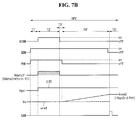
- FIGS. 7A and 7B show a process of sensing a change in the threshold voltage of the driving TFT according to an exemplary embodiment of the present invention.
- FIG. 8 shows that the change in the threshold voltage of the driving TFT appears as the difference in slope between the curves in the TFT linear region.
- a pixel P of this invention may comprise an OLED, a driving TFT (thin film transistor) DT, a storage capacitor Cst, a first switching TFT ST1, and a second switching TFT ST2.
- the OLED comprises an anode connected to a source node Ns, a cathode connected to an input terminal of a low-level operating voltage EVSS, and an organic compound layer positioned between the anode and the cathode.
- the driving TFT DT controls the amount of current input into the OLED based on a gate-source voltage Vgs.
- the driving TFT DT comprises a gate electrode connected to a gate node Ng, a drain electrode connected to an input terminal of a high-level operating voltage EVDD, and a source electrode connected to the source node Ns.
- the storage capacitor Cst is connected between the gate node Ng and the source node Ns to maintain the gate-source voltage Vgs of the driving TFT DT.
- the first switching TFT ST1 applies a sensing data voltage Vdata on a data line 14A to the gate node Ng in response to a scan control signal SCAN.
- the first switching TFT ST1 comprises a gate electrode connected to the first gate line 15A, a drain electrode connected to the data line 14A, and a source electrode connected to the gate node Ng.
- the second switching TFT ST2 switches on an electrical connection between the source node Ns and a sensing line 14B in response to a sensing control signal SEN.
- the second switching TFT ST2 comprises a gate electrode connected to a second gate line 15B, a drain electrode connected to the sensing line 14B, and a source node connected to the source node Ns.
- a sensing unit SU of this invention comprises a reference voltage control switch SW1, a sampling switch SW2, and a sample and hold circuit S/H.
- the reference voltage control switch SW1 is switched on in response to a reference voltage control signal PRE to connect an input terminal of a reference voltage Vref and the sensing line 14B.
- the sampling switch SW2 is switched on in response to a sampling control signal SAM to connect the sensing line 14B and the sample and hold circuit S/H.
- the sampling switch SW2 is turned on, the sample and hold circuit S/H samples and holds the source node voltage Vs of the driving TFT DT stored in a line capacitor LCa of the sensing line 14B as a sensing voltage Vsen and then passes it to an ADC.
- a parasitic capacitor present in the sensing line 14B may be substituted for the line capacitor LCa.
- An image display operation for internally compensating for a change in the mobility of the driving TFT will be described below in conjunction with an exemplary configuration of such a pixel and FIG. 6 .
- the image display operation is performed based on an image display data voltage reflecting the compensation voltage.
- a change in the mobility of the driving TFT is not compensated for in the compensation operation but compensated for in the image display operation. Accordingly, in the image display operation, an image is displayed, with the compensation of the changes in both the threshold voltage and mobility of the driving TFT.
- the image display operation comprises a initial period Ti, a sensing period Ts, an emission period Te.
- the reference voltage control switch SW1 remains ON to apply the reference voltage Vref to the sensing line 14B, and the sampling switch SW2 remains OFF.
- both the scan control signal SCAN and the sensing control signal SEN remain ON.
- the first switching TFT ST1 is turned on in response to the scan control signal SCAN of ON state to apply an image display data voltage to the gate electrode of the driving TFT DT
- the second switching TFT ST2 is turned on in response to the sensing control signal SEN of ON state and applies a reference voltage Vref to the source electrode of the driving TFT DT.
- the scan control signal SCAN remains ON, and the sensing control signal SEN is inverted to OFF.
- the first switching TFT ST1 remains ON and holds the voltage at the gate node Ng of the driving TFT DT at the image display data voltage.
- the second switching TFT ST2 is turned off, whereupon a current corresponding to a gate-source voltage difference Vgs, which is set in the initial period Ti, flows through the driving TFT DT. Accordingly, the voltage at the source node Ns of the driving TFT DT rises toward the image display data voltage applied to the gate electrode of the driving TFT DT according to a source-follower method, so that the gate-source voltage difference Vgs of the driving TFT DT is programmed to a desired gray level.
- both the scan control signal SCAN and the sensing control signal SEN remain OFF.
- the voltage at the gate node Ng of the driving TFT DT and the voltage at the source node Ns rise to a voltage level equal to or higher than the threshold voltage of the OLED while maintaining the voltage difference Vgs programmed in the sensing period Ts, and then maintain this voltage level.
- a drive current corresponding to the programmed gate-source voltage difference Vgs of the driving TFT DT flows through the OLED. As a result, the OLED emits light, thereby representing a desired gray level.
- a change in the mobility of the driving TFT DT is compensated for based on the principle that the source voltage Vs of the driving TFT DT is raised by capacitive coupling while the gate voltage Vg of the driving TFT DT is fixed at the image display data voltage during the sensing period Ts.
- the drive current which determines the light intensity (luminance) of the pixel, is proportional to the mobility ⁇ of the driving TFT DT and the gate-source voltage difference Vgs of the driving TFT DT programmed in the sensing period Ts.
- the source voltage Vs of the driving TFT DT rises at a first rate of rise toward the higher gate voltage Vg so that the gate-source voltage difference Vgs of the driving TFT DT is programmed to be relatively small.
- the source voltage Vs of the driving TFT DT rises at a second rate of rise (which is slower than the first rate of rise) toward the higher gate voltage Vg so that the gate-source voltage difference Vgs of the driving TFT DT is programmed to be relatively large. That is, the gate-source voltage is automatically programmed to be inversely proportional to the degree of mobility. As a result, luminance variations caused by differences in mobility ⁇ between pixels are compensated for.
- a compensation operation for compensating a change in the threshold voltage of the driving TFT will be described below in conjunction with the above-described exemplary configuration of a pixel and FIGS. 7A and 7B and FIG. 8 .
- a compensation operation comprises a first process for obtaining a first sensing voltage Vsen1 during a first compensation period SP1 shown in FIG. 7A , and a second process for obtaining a second sensing voltage Vsen2 during a second compensation period SP2 shown in FIG. 7B .
- the first compensation period SP1 and the second compensation period SP2 may be placed consecutively within one vertical blanking interval or separately in different vertical blanking intervals.
- the first compensation period SP1 may comprise a first programming period T2, a first sensing period T4, and a first sampling period T5.
- the first compensation period SP1 may further comprise a first source node initial period T3 in order to increase sensing accuracy.
- T1 is a first sensing line initial period for resetting the sensing line 14B to a reference voltage Vref in advance before the first programming period T2, and may be omitted.
- a scan control signal SCAN, sensing control signal SEN, and reference voltage signal PRE are all input as ON.
- the first switching TFT ST1 is turned on to apply a first data voltage for sensing Vdata1' to the gate node Ng of the driving TFT DT
- the second switching TFT ST2 and the reference voltage control switch SW1 are turned on to apply the reference voltage Vref to the source node Ns of the driving TFT DT.
- the gate-source voltage Vgs of the driving TFT DT is programmed to a first level LV1.
- the first data voltage for sensing Vdata1' reflects a threshold voltage component Vth(n-1) of the previous sensing period.
- the scan control signal SCAN is inverted to OFF, and the sensing control signal SEN and the reference voltage control signal PRE remain ON.
- the first switching TFT ST1 is turned off to make the gate node Ng of the driving TFT DT float, and the second switching TFT ST2 and the reference voltage control switch SW1 are turned on to constantly apply the reference voltage Vref to the source node Ns of the driving TFT DT.
- the source node Ns of the driving TFT DT is reset for the second time to the reference voltage Vref while the gate-source voltage Vgs of the driving TFT DT is held at the first level LV1.
- the reason why the source node Ns of the driving TFT DT is reset for the second time to the reference voltage Vref is because sensing accuracy can be increased by making the voltage at the start point of the first sensing period T4 equal for all pixels.
- the scan control signal SCAN is held at OFF level
- the sensing control signal SEN is held at ON level
- the reference voltage control signal PRE is inverted to OFF level.
- the first switching TFT ST1 is turned off to keep the gate node Ng of the driving TFT DT floating
- the reference voltage control switch SW1 is turned off to disconnect the source node Ns of the driving TFT DT from an input of the reference voltage Vref.
- a pixel current flows through the driving TFT DT by the gate-source voltage Vgs of the first level LV1, and the source node voltage Vs of the driving TFT DT rises due to this pixel current.
- the source node voltage Vs of the driving TFT DT is stored in the line capacitor LCa of the sensing line 14B by the turned-on second switching TFT ST2.
- the sensing control signal SEN is inverted to OFF level, and the sampling control signal SAM is input as ON level.
- the second switching TFT ST2 is turned off to release the electrical connection between the source node Ns of the driving TFT DT and the sensing line 14B.
- the sampling control switch SW2 is turned on to connect the sensing line 14B and the sample and hold circuit S/H, thereby sampling the source node voltage Vs of the driving TFT DT stored in the sensing line 14B as the first sensing voltage Vsen1.
- the first sensing voltage Vsen1 is converted to a first digital value by an ADC and then stored in an internal latch in the data drive circuit 12.
- the second compensation period SP2 may comprise a second programming period T2', a second sensing period T4', and a second sampling period T5'.
- the second compensation period SP2 may further comprise a second source node initial period T3' in order to increase sensing accuracy.
- T1' is a second sensing line initial period for resetting the sensing line 14B to a reference voltage Vref in advance before the second programming period T2', and may be omitted.
- a scan control signal SCAN, sensing control signal SEN, and reference voltage signal PRE are all input as ON.
- the first switching TFT ST1 is turned on to apply a second data voltage for sensing Vdata2' to the gate node Ng of the driving TFT DT
- the second switching TFT ST2 and the reference voltage control switch SW1 are turned on to apply the reference voltage Vref to the source node Ns of the driving TFT DT.
- the gate-source voltage Vgs of the driving TFT DT is programmed to a second level LV2.
- the second data voltage for sensing Vdata2' reflects a threshold voltage component Vth(n-1) of the previous sensing period.
- the scan control signal SCAN is inverted to OFF, and the sensing control signal SEN and the reference voltage control signal PRE remain ON.
- the first switching TFT ST1 is turned off to make the gate node Ng of the driving TFT DT float, and the second switching TFT ST2 and the reference voltage control switch SW1 are turned on to keep applying the reference voltage Vref to the source node Ns of the driving TFT DT.
- the source node Ns of the driving TFT DT is reset for the second time to the reference voltage Vref while the gate-source voltage Vgs of the driving TFT DT is held at the second level LV2.
- the reason why the source node Ns of the driving TFT DT is reset for the second time to the reference voltage Vref is because sensing accuracy can be increased by making the voltage at the start point of the second sensing period T4' equal for all pixels.
- the scan control signal SCAN is held at OFF level
- the sensing control signal SEN is held at ON level
- the reference voltage control signal PRE is inverted to OFF level.
- the first switching TFT ST1 is turned off to keep the gate node Ng of the driving TFT DT floating
- the reference voltage control switch sW1 is turned off to disconnect the source node Ns of the driving TFT DT from an input of the reference voltage Vref.
- a pixel current flows through the driving TFT DT by the gate-source voltage Vgs of the second level LV2, and the source node voltage Vs of the driving TFT DT rises due to this pixel current.
- the source node voltage Vs of the driving TFT DT is stored in the line capacitor LCa of the sensing line 14B by the turned-on second switching TFT ST2.
- the sensing control signal SEN is inverted to OFF level, and the sampling control signal SAM is input as ON level.
- the second switching TFT ST2 is turned off to release the electrical connection between the source node Ns of the driving TFT DT and the sensing line 14B.
- the sampling control switch SW2 is turned on to connect the sensing line 14B and the sample and hold circuit S/H, thereby sampling the source node voltage Vs of the driving TFT DT stored in the sensing line 14B as the second sensing voltage Vsen2.
- the second sensing voltage Vsen2 is converted to a second digital value by an ADC and then stored in an internal latch in the data drive circuit 12.
- the first and second sensing voltages Vsen1 and Vsen2 stored as digital values in the internal latch are transmitted to the timing controller 11.
- the timing controller 11 calculates the sensing ratio VSR between the first and second sensing voltages Vsen1 and Vsen2, and reads a change ⁇ Vth in the threshold voltage of the driving TFT DT from a look-up table by using a change in sensing ratio - which is obtained by subtracting the sensing ratio VSR from a preset initial sensing ratio VSRinit) - as a read address.
- a change in the threshold voltage of the driving TFT may be accurately sensed by canceling out a change in the mobility of the driving TFT commonly included in the first and second sensing voltages by using a sensing ratio VSR.
- a threshold voltage change ⁇ Vth is determined by a change in sensing ratio VSR.
- a change in the threshold voltage Vth of the driving TFT is represented as a difference in slope between the curves in the TFT linear region in which Vgs is lower than Vth.
- the voltage values in the TFT linear region are sensed in order to reduce the time taken for the sensing.
- a sensing voltage comprises the change in mobility as well as a change in threshold voltage, and the change in mobility has a much greater effect on the sensing voltage, thereby making it possible to precisely detect a change in threshold voltage.
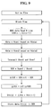
- FIG. 9 shows a method for sensing a change in the threshold voltage of the driving TFT according to an exemplary embodiment of the present invention.
- FIG. 10 shows a vertical blanking interval in one frame during which a change in the threshold voltage of the driving TFT is sensed.
- first and second sensing voltages are obtained by fast sensing in the TFT linear region, and a change in the threshold voltage of the driving TFT is obtained based on the sensing ratio between the sensing voltages.
- a number of processes for deducing a change in threshold voltage such as programming, source node resetting, sensing, and sampling, may be performed during the vertical blanking interval. That is, it is possible to sense a change in the threshold voltage of the driving TFT DT during real-time operation, without the need of arranging a time during power-on or power-off in order to sense a threshold voltage change, thereby improving compensation performance.
- the vertical blanking interval indicates the time between active intervals for image display during which data for image display is not written, as illustrated in FIG. 10 .
- a data enable signal DE continues to remain at low logic level L.
- the data enable signal DE is at low logic level, data writing is paused.
Landscapes
- Engineering & Computer Science (AREA)
- Physics & Mathematics (AREA)
- Computer Hardware Design (AREA)
- General Physics & Mathematics (AREA)
- Theoretical Computer Science (AREA)
- Control Of El Displays (AREA)
- Control Of Indicators Other Than Cathode Ray Tubes (AREA)
Abstract
Description
- The present invention relates to an organic light emitting display, and more particularly, to a device and method for sensing the threshold voltage of a driving TFT included in an organic light emitting display.
- An active-matrix organic light emitting display comprises organic light emitting diodes OLEDs that emit light themselves, and has the advantages of fast response time, high luminous efficiency, high luminance, and wide viewing angle.
- An OLED, which is a self-luminous device, comprises an anode and a cathode, and organic compound layers HIL, HTL, EML, ETL, and EIL formed between the anode and cathode. The organic compound layers comprise a hole injection layer HIL, a hole transport layer HTL, an emission layer EML, an electron transport layer ETL, and an electron injection layer EIL. When an operating voltage is applied to the anode and the cathode, a hole passing through the hole transport layer HTL and an electron passing through the electron transport layer ETL move to the emission layer EML, forming an exciton. As a result, the emission layer EML generates visible light.
- In an organic light emitting diode display, pixels each comprising an organic light emitting diode are arranged in a matrix, and the luminance of the pixels is adjusted based on the grayscale of video data. Each individual pixel comprises a driving TFT (thin-film transistor) that controls the drive current flowing through the OLED. The electrical characteristic of the driving TFT, such as threshold voltage, mobility, etc., may vary from pixel to pixel because of the process condition, driving environment, etc. Such variation in the electrical characteristics of the driving TFT causes luminance differences between the pixels. As a solution to this problem, the technology that senses the characteristic parameters (threshold voltage, mobility, etc.) of the driving TFT of each pixel and corrects image data based on the sensing results is known.
- In the conventional art, as shown in
FIG. 1 , a driving TFT DT is operated according to a source follower method, and then the source node voltage Vs of the driving TFT DT is detected as a sensing voltage Vsen at the time ta when the gate-source voltage Vgs of the driving TFT DT reaches saturation state by an electric current flowing through the driving TFT DT, in order to sense a change in the threshold voltage Vth of the driving TFT DT. However, a long period of time is needed in order for the gate-source voltage Vgs of the driving TFT DT to reach the threshold voltage Vth of the driving TFT DT. Accordingly, in the conventional art, it is not possible to sense a change in the threshold voltage Vth of the driving TFT DT during real-time operation. - Accordingly, the present invention is directed to a device and method for sensing the threshold voltage of a driving TFT included in an organic light emitting display so that a change in the threshold voltage of the driving TFT is sensed during real-time operation by reducing sensing time.
- The object is solved by the features of the independent claims.
- An exemplary embodiment of the present invention provides a device for sensing threshold voltage in an organic light emitting display with a plurality of pixels each having an OLED and a driving TFT for controlling the amount of light emitted by the OLED, the device comprising: a data drive circuit and a timing controller. The data drive circuit applies a first data voltage for sensing to the gate node of the driving TFT during a first programming period, obtains the source node voltage of the driving TFT as a first sensing voltage during a first sensing period in which the gate-source voltage of the driving TFT is constantly held at a first value higher than the threshold voltage of the driving TFT, applies a second data voltage for sensing to the gate node of the driving TFT during a second programming period, and obtains the source node voltage of the driving TFT as a second sensing voltage during a second sensing period in which the gate-source voltage of the driving TFT is constantly held at a second value higher than the threshold voltage of the driving TFT. The timing controller calculates an nth sensing ratio (n is a positive integer) based on the ratio between the first and second sensing voltages, calculates a change in sensing ratio by comparing the nth sensing ratio with a preset initial sensing ratio, and then obtains a change in the threshold voltage of the driving TFT based on the change in sensing ratio.
- Preferably, the first programing period and the first sensing period are included in a first compensation period
- Preferably, the second programming period and the second sensing period are included in a second compensation period.
- Preferably, the first and second compensation periods are placed in a vertical blanking interval.
- Preferably, the vertical blanking interval is the time between active intervals for image display
- Preferably, data for image display is not written during the vertical blanking interval.
- Preferably, the first and second compensation periods are arranged consecutively in the same vertical blanking interval.
- Preferably, the first and second compensation periods are placed separately in different vertical blanking intervals.
- Preferably, the data drive circuit may be adapted to supply a reference voltage to the source node of the driving TFT during a first initial period between the first programming period and the first sensing period.
- Preferably, the data drive circuit may be adapted to supply the reference voltage to the source node of the driving TFT during a second initial period between the second programming period and the second sensing period.
- Preferably, a gate drive circuit may be adapted to generate a scan control signal and/or a sensing control signal.
- Preferably, each pixel may comprise a first switching TFT adapted to be turned on in response to the scan control signal to connect a data line connected to the data drive circuit to the gate node of the driving TFT,
- Preferably, each pixel may comprise a second switching TFT adapted to be turned on in response to the sensing control signal to connect the source node of the driving TFT to a sensing line connected to a sensing unit in the data drive circuit, and a storage capacitor connected between the gate node and source node of the driving TFT.
- Preferably, the sensing unit may comprise a reference voltage control switch adapted to be switched on in response to a reference voltage control signal to connect a reference voltage input terminal and the sensing line, and a sampling control switch adapted to be switched on in response to a sampling control signal (SAM) to connect the sensing line and a sample and hold circuit.
- Preferably, the scan control signal is applied at ON level during the first and second programming periods,
- Preferably, the sensing control signal is applied at ON level during the first and second programming periods, the first and second initial periods, and the first and second sensing periods
- Preferably, the reference voltage control signal is applied at ON level during the first and second programming periods and the first and second initial periods.
- Preferably, the sampling control signal is applied at ON level during a first sampling period after the first sensing period and a second sampling period after the second sensing period.
- Another exemplary embodiment of the present invention provides a method for sensing threshold voltage in organic light emitting display with a plurality of pixels each having an OLED and a driving TFT for controlling the amount of light emitted by the OLED, the method comprising: applying a first data voltage for sensing to the gate node of the driving TFT during a first programming period and obtaining the source node voltage of the driving TFT as a first sensing voltage during a first sensing period in which the gate-source voltage of the driving TFT is constantly held at a first value higher than the threshold voltage of the driving TFT; applying a second data voltage for sensing to the gate node of the driving TFT during a second programming period and obtaining the source node voltage of the driving TFT as a second sensing voltage during a second sensing period in which the gate-source voltage of the driving TFT is constantly held at a second value higher than the threshold voltage of the driving TFT; and calculating an nth sensing ratio (n is a positive integer) based on the ratio between the first and second sensing voltages, calculating a change in sensing ratio by comparing the nth sensing ratio with a preset initial sensing ratio, and then obtaining a change in the threshold voltage of the driving TFT based on the change in sensing ratio.
- Preferably, the first programing period and the first sensing period are included in a first compensation period and the second programming period and the second sensing period are included in a second compensation period.
- Preferably, the first and second compensation periods are placed in a vertical blanking interval, and the vertical blanking interval is the time between active intervals for image display, wherein data for image display is not written during the vertical blanking interval.
- Preferably, the first and second compensation periods are placed consecutively in the same vertical blanking interval or the first and second compensation periods are placed separately in different vertical blanking intervals.
- Preferably, the method may further comprise supplying a reference voltage to the source node of the driving TFT during a first initial period between the first programming period and the first sensing period and supplying the reference voltage to the source node of the driving TFT during a second initial period between the second programming period and the second sensing period.
- The accompanying drawings, which are included to provide a further understanding of the invention and are incorporated in and constitute a part of this specification, illustrate embodiments of the invention and together with the description serve to explain the principles of the invention. In the drawings:
-
FIG. 1 is a view showing a conventional technology for sensing the threshold voltage of a driving TFT according to a source follower method; -
FIG. 2 is a view schematically showing an organic light emitting display according to an exemplary embodiment of the present invention; -
FIG. 3 is a view showing an example of the configuration of a pixel array and a data driver IC; -
FIG. 4 is a view showing the principle for deducing a change in the threshold voltage of the driving TFT based on a sensing ratio; -
FIG. 5 is a circuit diagram showing detailed configurations of a pixel and a sensing unit according to an exemplary embodiment of the present invention; -
FIG. 6 is a waveform diagram showing the compensation of a change in the mobility of the driving TFT according to an exemplary embodiment of the present invention; -
FIGS. 7A and7B are waveform diagrams showing a process of sensing a change in the threshold voltage of the driving TFT according to an exemplary embodiment of the present invention; -
FIG. 8 is a view showing that the change in the threshold voltage of the driving TFT appears as the difference in slope between the curves in the TFT linear region; -
FIG. 9 shows a method for sensing a change in the threshold voltage of the driving TFT according to an exemplary embodiment of the present invention; and -
FIG. 10 shows a vertical blanking interval in one frame during which a change in the threshold voltage of the driving TFT is sensed. - Hereinafter, exemplary embodiments of the present invention will be described in detail with reference to the accompanying drawings. Throughout the specification, like numbers refer to like elements. In describing the present invention, when it is deemed that a detailed description of known functions or configurations may unnecessarily obscure the subject matter of the present invention, the detailed description will be omitted
-
FIG. 2 is a view schematically showing an organic light emitting display according to an exemplary embodiment of the present invention.FIG. 3 is a view showing an example of the configuration of a pixel array and a data driver IC.FIG. 4 is a view showing the principle for deriving a change in the threshold voltage of the driving TFT based on a sensing ratio. - Referring to
FIGS. 2 and3 , an organic light emitting display according to an exemplary embodiment of the present invention may comprise adisplay panel 10, atiming controller 11, adata drive circuit 12, agate drive circuit 13, and amemory 16. - A plurality of data lines and
sensing lines gate lines 15 intersect each other on thedisplay panel 10, and pixels P are arranged in a matrix at the intersections. The gate lines 15 comprise a plurality offirst gate lines 15A sequentially supplied with a scan control signal (SCAN ofFIG. 5 ) and a plurality of second gate lines 15B sequentially supplied with a sensing control signal (SEN ofFIG. 5 ). - Each pixel P may be connected to any one of the data lines 14A, any one of the sensing lines 14B, any one of the
first gate lines 15A, and any one of the second gate lines 15B. Each pixel P may be connected to adata line 14A in response to a scan control signal SCAN input through afirst gate line 15A, and may be connected to asensing line 14B in response to a sensing control signal SEN input through asecond gate line 15B. - Each pixel P is supplied with a high-level operating voltage EVDD and a low-level operating voltage EVSS from a power generator (not shown). Each pixel P of this invention may comprise an OLED and a driving TFT that drives the OLED. The driving TFT may be implemented as p-type or n-type. Also, a semiconductor layer of the driving TFT may comprise amorphous silicon, polysilicon, or oxide.
- Each pixel P displays an image, and may operate differently in an image display operation for internally compensating for a change in the mobility of the driving TFT and in a compensation operation for sensing and compensating for a change in the threshold voltage of the driving TFT. The compensation operation of this invention may be performed for a predetermined amount of time during power-on or power-off. Particularly, the compensation operation of this invention may reduce the time taken to sense a change in the threshold voltage of the driving TFT by a method to be described later. Thus, it is possible to sense a change in the threshold voltage of the driving TFT during vertical blanking intervals of a real-time operation, that is, image display operation.
- The image display operation and the compensation operation may be implemented depending on the operation of the data drive
circuit 12 andgate drive circuit 13 under the control of thetiming controller 11. - The data drive
circuit 12 comprises at least one data driver IC (integrated circuit) SDIC. The data driver IC (SDIC) may comprise a plurality of digital-to-analog converters (hereinafter, DAC) 121 connected todata lines 14A, a plurality of sensingunits 122 connected to sensinglines 14B, a multiplexer (MUX) 123 that selectively connects thesensing units 122 to an analog-to-digital converter (hereinafter, ADC), and ashift register 124 that generates a selection control signal and sequentially turns on switches SS1 to SSk in theMUX 123. - In the compensation operation, the DACs generate a data voltage for sensing and supply it to the data lines 14A, under the control of the
timing controller 11. In the image display operation, the DACs generate a data voltage for image display and supply it to the data lines 14A, under the control of thetiming controller 11. - The sensing
units SU# 1 to SU#k may be connected to thesensing lines 14B on a one-to-one basis. The sensingunits SU# 1 to SU#k may supply a reference voltage to thesensing lines 14B or read a sensing voltage stored in thesensing lines 14B and supply it to the ADC, under the control of thetiming controller 11. - The ADC converts a sensing voltage selectively input through the
MUX 123 to a digital value and transmits it to thetiming controller 11. - The
gate drive circuit 13 may generate a scan control signal corresponding to the image display operation or compensation operation and then supply it to the first gate lines 15Aline by line, under the control of thetiming controller 11. Thegate drive circuit 13 generates a sensing control signal corresponding to the image display operation or compensation operation and then supplies it to the second gate lines 15Bline by line, under the control of thetiming controller 11. - The
timing controller 11 generates a data control signal DDC for controlling the operation timing of the data drivecircuit 12 and a gate control signal GDC for controlling the operation timing of the gate drive circuit 131, based on timing signals such as a vertical synchronization signal Vsync, a horizontal synchronization signal Hsync, a dot clock signal DCLK, and a data enable signal DE. Thetiming controller 11 may differentiate between the image display operation and the compensation operation based on a predetermined reference signal (driving power enable signal, a vertical synchronization signal, a data enable signal, etc.), and generate a data control signal DDC and gate control signal GDC corresponding to each of the image display operation and compensation operation. Moreover, thetiming controller 11 may further generate relevant switching control signals CON (including PRE and SAM ofFIG. 5 ) in order to operate internal switches in each sensingunit SU# 1 to SU#k for the image display operation and compensation operation. - As shown in
FIG. 4 , thetiming controller 11 obtains a first sensing voltage Vsen1 and a second sensing voltage Vsen2 by sensing a change in the threshold voltage of the driving TFT twice for each pixel, and obtains a change in the threshold voltage of the driving TFT based on the sensing ratio VSR between the first and second sensing voltages Vsen1 and Vsen2. InFIG. 4 , Vsen1_init indicates a first initial sensing voltage of when a first data voltage for sensing is applied, Vsen2_init indicates a second initial sensed voltage of when a second data voltage for sensing is applied. VSRinit is an initial sensing ratio, which is equal to the first initial sensing voltage Vsen1_init divided by the second initial sensing voltage Vsen2_init. The initial sensing ratio VSRinit may vary depending on the product model and specification, and is preset at the time of product release and stored in the internal memory of the display device. - In the present invention, when there is a change in the threshold voltage of the driving TFT due to driving stress, different sensing data voltages are applied to each pixel, and the source node voltage of the driving TFT is acquired as the first and second sensing voltages while the gate-source voltage of the driving TFT is higher than the threshold voltage of the driving TFT. The first and second sensing voltages comprise a change in the mobility of the driving TFT, as well as a change in the threshold voltage of the driving TFT. Thus, in the present invention, by calculating the sensing ratio between the first and second sensing voltages, the change in the mobility of the driving TFT commonly included in the first and second sensing voltages may be canceled out, and only the change in the threshold voltage of the driving TFT may be obtained. Conventionally, the source node voltage of the driving TFT is sensed at the timing when the gate-source voltage of the driving TFT is saturated at the threshold voltage of the driving TFT. This means that the sensing requires a very long time, making it impossible to sense a change in the threshold voltage of the driving TFT during a vertical blanking interval in the image display operation. However, if the sensing is done while the gate-source voltage of the driving TFT is higher than the threshold voltage of the driving TFT, as in the present invention, the total time taken for the sensing is reduced to 1/10 of the conventional art even if the sensing is done twice. Accordingly, a change in the threshold voltage of the driving TFT can be adequately sensed during the vertical blanking interval in the image display operation.
- In the compensation operation, the
timing controller 11 calculates an nth sensing ratio (n is a positive integer) based on the ratio between the first and second sensing voltages, calculates a change in sensing ratio by comparing the nth sensing ratio with a preset initial sensing ratio, and then obtains a change in the threshold voltage based on the change in sensing ratio. Thetiming controller 11 may properly update an (n-1)th compensation value stored in thememory 16 based on the obtained threshold voltage change. - In the compensation operation, the
timing controller 11 may transmit first and second compensation data corresponding to the first and second data voltage for sensings to the data drivecircuit 12. Here, the first and second compensation data reflects the change in the threshold voltage of the driving TFT that was sensed in the previous sensing period. In the image display operation, thetiming controller 11 may transmit image data RGB corresponding to the image display data voltage. Here, the image data RGB may be modulated in such a way as to compensate for the change in the threshold voltage of the driving TFT that was sensed in the previous sensing period. -
FIG. 5 shows detailed configurations of a pixel and a sensing unit according to an exemplary embodiment of the present invention.FIG. 6 shows the compensation of a change in the mobility of the driving TFT according to an exemplary embodiment of the present invention. -
FIGS. 7A and7B show a process of sensing a change in the threshold voltage of the driving TFT according to an exemplary embodiment of the present invention.FIG. 8 shows that the change in the threshold voltage of the driving TFT appears as the difference in slope between the curves in the TFT linear region. - Referring to
FIG. 5 , a pixel P of this invention may comprise an OLED, a driving TFT (thin film transistor) DT, a storage capacitor Cst, a first switching TFT ST1, and a second switching TFT ST2. - The OLED comprises an anode connected to a source node Ns, a cathode connected to an input terminal of a low-level operating voltage EVSS, and an organic compound layer positioned between the anode and the cathode.
- The driving TFT DT controls the amount of current input into the OLED based on a gate-source voltage Vgs. The driving TFT DT comprises a gate electrode connected to a gate node Ng, a drain electrode connected to an input terminal of a high-level operating voltage EVDD, and a source electrode connected to the source node Ns. The storage capacitor Cst is connected between the gate node Ng and the source node Ns to maintain the gate-source voltage Vgs of the driving TFT DT. The first switching TFT ST1 applies a sensing data voltage Vdata on a
data line 14A to the gate node Ng in response to a scan control signal SCAN. The first switching TFT ST1 comprises a gate electrode connected to thefirst gate line 15A, a drain electrode connected to thedata line 14A, and a source electrode connected to the gate node Ng. The second switching TFT ST2 switches on an electrical connection between the source node Ns and asensing line 14B in response to a sensing control signal SEN. The second switching TFT ST2 comprises a gate electrode connected to asecond gate line 15B, a drain electrode connected to thesensing line 14B, and a source node connected to the source node Ns. - Also, a sensing unit SU of this invention comprises a reference voltage control switch SW1, a sampling switch SW2, and a sample and hold circuit S/H.
- The reference voltage control switch SW1 is switched on in response to a reference voltage control signal PRE to connect an input terminal of a reference voltage Vref and the
sensing line 14B. The sampling switch SW2 is switched on in response to a sampling control signal SAM to connect thesensing line 14B and the sample and hold circuit S/H. When the sampling switch SW2 is turned on, the sample and hold circuit S/H samples and holds the source node voltage Vs of the driving TFT DT stored in a line capacitor LCa of thesensing line 14B as a sensing voltage Vsen and then passes it to an ADC. Here, a parasitic capacitor present in thesensing line 14B may be substituted for the line capacitor LCa. - An image display operation for internally compensating for a change in the mobility of the driving TFT will be described below in conjunction with an exemplary configuration of such a pixel and
FIG. 6 . When a compensation value corresponding to a threshold voltage change is obtained in the compensation operation for sensing a change in threshold voltage, the image display operation is performed based on an image display data voltage reflecting the compensation voltage. A change in the mobility of the driving TFT is not compensated for in the compensation operation but compensated for in the image display operation. Accordingly, in the image display operation, an image is displayed, with the compensation of the changes in both the threshold voltage and mobility of the driving TFT. - The image display operation comprises a initial period Ti, a sensing period Ts, an emission period Te. During the image display operation, the reference voltage control switch SW1 remains ON to apply the reference voltage Vref to the
sensing line 14B, and the sampling switch SW2 remains OFF. - In the initial period Ti, both the scan control signal SCAN and the sensing control signal SEN remain ON. The first switching TFT ST1 is turned on in response to the scan control signal SCAN of ON state to apply an image display data voltage to the gate electrode of the driving TFT DT, and the second switching TFT ST2 is turned on in response to the sensing control signal SEN of ON state and applies a reference voltage Vref to the source electrode of the driving TFT DT.
- In the sensing period Ts, the scan control signal SCAN remains ON, and the sensing control signal SEN is inverted to OFF. The first switching TFT ST1 remains ON and holds the voltage at the gate node Ng of the driving TFT DT at the image display data voltage. The second switching TFT ST2 is turned off, whereupon a current corresponding to a gate-source voltage difference Vgs, which is set in the initial period Ti, flows through the driving TFT DT. Accordingly, the voltage at the source node Ns of the driving TFT DT rises toward the image display data voltage applied to the gate electrode of the driving TFT DT according to a source-follower method, so that the gate-source voltage difference Vgs of the driving TFT DT is programmed to a desired gray level.
- In the emission period Te, both the scan control signal SCAN and the sensing control signal SEN remain OFF. The voltage at the gate node Ng of the driving TFT DT and the voltage at the source node Ns rise to a voltage level equal to or higher than the threshold voltage of the OLED while maintaining the voltage difference Vgs programmed in the sensing period Ts, and then maintain this voltage level. A drive current corresponding to the programmed gate-source voltage difference Vgs of the driving TFT DT flows through the OLED. As a result, the OLED emits light, thereby representing a desired gray level.
- As such, a change in the mobility of the driving TFT DT is compensated for based on the principle that the source voltage Vs of the driving TFT DT is raised by capacitive coupling while the gate voltage Vg of the driving TFT DT is fixed at the image display data voltage during the sensing period Ts. The drive current, which determines the light intensity (luminance) of the pixel, is proportional to the mobility µ of the driving TFT DT and the gate-source voltage difference Vgs of the driving TFT DT programmed in the sensing period Ts. During the sensing period Ts, in the case of a pixel with high mobility µ, the source voltage Vs of the driving TFT DT rises at a first rate of rise toward the higher gate voltage Vg so that the gate-source voltage difference Vgs of the driving TFT DT is programmed to be relatively small. On the contrary, during the sensing period Ts, in the case of a pixel with low mobility µ, the source voltage Vs of the driving TFT DT rises at a second rate of rise (which is slower than the first rate of rise) toward the higher gate voltage Vg so that the gate-source voltage difference Vgs of the driving TFT DT is programmed to be relatively large. That is, the gate-source voltage is automatically programmed to be inversely proportional to the degree of mobility. As a result, luminance variations caused by differences in mobility µ between pixels are compensated for.
- A compensation operation for compensating a change in the threshold voltage of the driving TFT will be described below in conjunction with the above-described exemplary configuration of a pixel and
FIGS. 7A and7B andFIG. 8 . - A compensation operation comprises a first process for obtaining a first sensing voltage Vsen1 during a first compensation period SP1 shown in
FIG. 7A , and a second process for obtaining a second sensing voltage Vsen2 during a second compensation period SP2 shown inFIG. 7B . Here, the first compensation period SP1 and the second compensation period SP2 may be placed consecutively within one vertical blanking interval or separately in different vertical blanking intervals. - As shown in
FIG. 7A , the first compensation period SP1 may comprise a first programming period T2, a first sensing period T4, and a first sampling period T5. The first compensation period SP1 may further comprise a first source node initial period T3 in order to increase sensing accuracy. InFIG. 7A , "T1" is a first sensing line initial period for resetting thesensing line 14B to a reference voltage Vref in advance before the first programming period T2, and may be omitted. - In the first programming period T2, a scan control signal SCAN, sensing control signal SEN, and reference voltage signal PRE are all input as ON. In the first programming period T2, the first switching TFT ST1 is turned on to apply a first data voltage for sensing Vdata1' to the gate node Ng of the driving TFT DT, and the second switching TFT ST2 and the reference voltage control switch SW1 are turned on to apply the reference voltage Vref to the source node Ns of the driving TFT DT. As a result, the gate-source voltage Vgs of the driving TFT DT is programmed to a first level LV1. Here, the first data voltage for sensing Vdata1' reflects a threshold voltage component Vth(n-1) of the previous sensing period.
- In the first source node initial period T3, the scan control signal SCAN is inverted to OFF, and the sensing control signal SEN and the reference voltage control signal PRE remain ON. In the first source node initial period T3, the first switching TFT ST1 is turned off to make the gate node Ng of the driving TFT DT float, and the second switching TFT ST2 and the reference voltage control switch SW1 are turned on to constantly apply the reference voltage Vref to the source node Ns of the driving TFT DT. As a result, the source node Ns of the driving TFT DT is reset for the second time to the reference voltage Vref while the gate-source voltage Vgs of the driving TFT DT is held at the first level LV1. The reason why the source node Ns of the driving TFT DT is reset for the second time to the reference voltage Vref is because sensing accuracy can be increased by making the voltage at the start point of the first sensing period T4 equal for all pixels.
- In the first sensing period T4, the scan control signal SCAN is held at OFF level, the sensing control signal SEN is held at ON level, and the reference voltage control signal PRE is inverted to OFF level. In the first sensing period T4, the first switching TFT ST1 is turned off to keep the gate node Ng of the driving TFT DT floating, and the reference voltage control switch SW1 is turned off to disconnect the source node Ns of the driving TFT DT from an input of the reference voltage Vref. In this state, a pixel current flows through the driving TFT DT by the gate-source voltage Vgs of the first level LV1, and the source node voltage Vs of the driving TFT DT rises due to this pixel current. The source node voltage Vs of the driving TFT DT is stored in the line capacitor LCa of the
sensing line 14B by the turned-on second switching TFT ST2. - In the first sampling period T5, the sensing control signal SEN is inverted to OFF level, and the sampling control signal SAM is input as ON level. In the first sampling period T5, the second switching TFT ST2 is turned off to release the electrical connection between the source node Ns of the driving TFT DT and the
sensing line 14B. Also, the sampling control switch SW2 is turned on to connect thesensing line 14B and the sample and hold circuit S/H, thereby sampling the source node voltage Vs of the driving TFT DT stored in thesensing line 14B as the first sensing voltage Vsen1. The first sensing voltage Vsen1 is converted to a first digital value by an ADC and then stored in an internal latch in the data drivecircuit 12. - As shown in
FIG. 7B , the second compensation period SP2 may comprise a second programming period T2', a second sensing period T4', and a second sampling period T5'. The second compensation period SP2 may further comprise a second source node initial period T3' in order to increase sensing accuracy. InFIG. 7B , T1' is a second sensing line initial period for resetting thesensing line 14B to a reference voltage Vref in advance before the second programming period T2', and may be omitted. - In the second programming period T2', a scan control signal SCAN, sensing control signal SEN, and reference voltage signal PRE are all input as ON. In the second programming period T2', the first switching TFT ST1 is turned on to apply a second data voltage for sensing Vdata2' to the gate node Ng of the driving TFT DT, and the second switching TFT ST2 and the reference voltage control switch SW1 are turned on to apply the reference voltage Vref to the source node Ns of the driving TFT DT. As a result, the gate-source voltage Vgs of the driving TFT DT is programmed to a second level LV2. Here, the second data voltage for sensing Vdata2' reflects a threshold voltage component Vth(n-1) of the previous sensing period.
- In the second source node initial period T3', the scan control signal SCAN is inverted to OFF, and the sensing control signal SEN and the reference voltage control signal PRE remain ON. In the second source node initial period T3', the first switching TFT ST1 is turned off to make the gate node Ng of the driving TFT DT float, and the second switching TFT ST2 and the reference voltage control switch SW1 are turned on to keep applying the reference voltage Vref to the source node Ns of the driving TFT DT. As a result, the source node Ns of the driving TFT DT is reset for the second time to the reference voltage Vref while the gate-source voltage Vgs of the driving TFT DT is held at the second level LV2. The reason why the source node Ns of the driving TFT DT is reset for the second time to the reference voltage Vref is because sensing accuracy can be increased by making the voltage at the start point of the second sensing period T4' equal for all pixels.
- In the second sensing period T4', the scan control signal SCAN is held at OFF level, the sensing control signal SEN is held at ON level, and the reference voltage control signal PRE is inverted to OFF level. In the second sensing period T4', the first switching TFT ST1 is turned off to keep the gate node Ng of the driving TFT DT floating, and the reference voltage control switch sW1 is turned off to disconnect the source node Ns of the driving TFT DT from an input of the reference voltage Vref. In this state, a pixel current flows through the driving TFT DT by the gate-source voltage Vgs of the second level LV2, and the source node voltage Vs of the driving TFT DT rises due to this pixel current. The source node voltage Vs of the driving TFT DT is stored in the line capacitor LCa of the
sensing line 14B by the turned-on second switching TFT ST2. - In the second sampling period T5', the sensing control signal SEN is inverted to OFF level, and the sampling control signal SAM is input as ON level. In the second sampling period T5', the second switching TFT ST2 is turned off to release the electrical connection between the source node Ns of the driving TFT DT and the
sensing line 14B. Also, the sampling control switch SW2 is turned on to connect thesensing line 14B and the sample and hold circuit S/H, thereby sampling the source node voltage Vs of the driving TFT DT stored in thesensing line 14B as the second sensing voltage Vsen2. The second sensing voltage Vsen2 is converted to a second digital value by an ADC and then stored in an internal latch in the data drivecircuit 12. - The first and second sensing voltages Vsen1 and Vsen2 stored as digital values in the internal latch are transmitted to the
timing controller 11. Thetiming controller 11 calculates the sensing ratio VSR between the first and second sensing voltages Vsen1 and Vsen2, and reads a change ΔVth in the threshold voltage of the driving TFT DT from a look-up table by using a change in sensing ratio - which is obtained by subtracting the sensing ratio VSR from a preset initial sensing ratio VSRinit) - as a read address. - In the present invention, a change in the threshold voltage of the driving TFT may be accurately sensed by canceling out a change in the mobility of the driving TFT commonly included in the first and second sensing voltages by using a sensing ratio VSR. According to the present invention, a threshold voltage change ΔVth is determined by a change in sensing ratio VSR. Even for pixels having driving TFTs with the same mobility, a change in the threshold voltage Vth of the driving TFT is represented as a difference in slope between the curves in the TFT linear region in which Vgs is lower than Vth. In the present invention, the voltage values in the TFT linear region are sensed in order to reduce the time taken for the sensing.
- In the present invention, since a change in mobility is linearly and internally compensated for during the image display operation, accurate and fast sensing may be done in the TFT linear region during the compensation operation. In cases where fast sensing is done as discussed above without linearly compensating for a change in mobility, a sensing voltage comprises the change in mobility as well as a change in threshold voltage, and the change in mobility has a much greater effect on the sensing voltage, thereby making it possible to precisely detect a change in threshold voltage.
-
FIG. 9 shows a method for sensing a change in the threshold voltage of the driving TFT according to an exemplary embodiment of the present invention.FIG. 10 shows a vertical blanking interval in one frame during which a change in the threshold voltage of the driving TFT is sensed. - Referring to
FIG. 9 , in the present invention, first and second sensing voltages are obtained by fast sensing in the TFT linear region, and a change in the threshold voltage of the driving TFT is obtained based on the sensing ratio between the sensing voltages. Thus, a number of processes for deducing a change in threshold voltage, such as programming, source node resetting, sensing, and sampling, may be performed during the vertical blanking interval. That is, it is possible to sense a change in the threshold voltage of the driving TFT DT during real-time operation, without the need of arranging a time during power-on or power-off in order to sense a threshold voltage change, thereby improving compensation performance. - Here, the vertical blanking interval indicates the time between active intervals for image display during which data for image display is not written, as illustrated in
FIG. 10 . During the vertical blanking interval, a data enable signal DE continues to remain at low logic level L. When the data enable signal DE is at low logic level, data writing is paused. - Throughout the description, it should be understood by those skilled in the art that various changes and modifications are possible without departing from the technical principles of the present invention. Therefore, the technical scope of the present invention is not limited to the detailed descriptions in this specification but should be defined by the scope of the appended claims.
Claims (15)
- A device for sensing the threshold voltage (Vth) of a driving TFT (DT) included in an organic light emitting display with a plurality of pixels (P) each having an OLED and a driving TFT (DT) for controlling the amount of light emitted by the OLED, the device comprising:a data drive circuit (12) adapted to apply a first data voltage (Vdata1') for sensing to the gate node (Ng) of the driving TFT (DT) during a first programming period (T2), obtain the source node voltage (Vgs) of the driving TFT (DT) as a first sensing voltage (Vsen1) during a first sensing period (T4) in which the gate-source voltage (Vgs) of the driving TFT (DT) is constantly held at a first value higher than the threshold voltage (Vth) of the driving TFT (DT), apply a second data voltage (Vdata2') for sensing to the gate node (Ng) of the driving TFT (DT) during a second programming period (T2'), and obtain the source node voltage (Vs) of the driving TFT (DT) as a second sensing voltage (Vsen2) during a second sensing period (T4') in which the gate-source voltage (Vgs) of the driving TFT (DT) is constantly held at a second value higher than the threshold voltage of the driving TFT (DT); anda timing controller (11) adapted to calculate an nth sensing ratio (VSR), n is a positive integer, based on the ratio between the first and second sensing voltages (Vsen1/Vsen2), calculate a change in sensing ratio (VSR) by comparing the nth sensing ratio with a preset initial sensing ratio, and then obtain a change in the threshold voltage of the driving TFT based on the change in sensing ratio.
- The device of claim 1, wherein the first programing period (T2) and the first sensing period (T4) are included in a first compensation period (SP1), and the second programming period (T2') and the second sensing period (T4') are included in a second compensation period (SP2).
- The device of claim 2, wherein the first and second compensation periods (Sp1, SP2) are placed in a vertical blanking interval, and the vertical blanking interval is the time between active intervals for image display, wherein data for image display is not written during the vertical blanking interval.
- The device of claims 2 or 3, wherein the first and second compensation periods (SP1, SP2) are arranged consecutively in the same vertical blanking interval or the first and second compensation periods (SP1, SP2) are placed separately in different vertical blanking intervals.
- The device as claimed in any one of the preceding claims, wherein the data drive circuit (12) is adapted to supply a reference voltage (Vref) to the source node (Ns) of the driving TFT (DT) during a first initial period (T3) between the first programming period (T2) and the first sensing period (T4), and to supply the reference voltage (Vref) to the source node (Ns) of the driving TFT (DT) during a second initial period (T3') between the second programming period (T2') and the second sensing period (T4').
- The device as claimed in any one of the preceding claims, further comprising a gate drive circuit (13) adapted to generate a scan control signal (SCAN) and a sensing control signal (SEN).
- The device as claimed in any one of the preceding claims, wherein each pixel (P) further comprises a first switching TFT (ST1) adapted to be turned on in response to the scan control signal (SCAN) to connect a data line (14A) connected to the data drive circuit (12) to the gate node (Ng) of the driving TFT (DT), a second switching TFT (ST2) adapted to be turned on in response to the sensing control signal (SEN) to connect the source node (Ns) of the driving TFT (DT) to a sensing line (14B) connected to a sensing unit (SU) in the data drive circuit (12), and a storage capacitor (Cst) connected between the gate node (Ng) and source node (Ns) of the driving TFT.
- The device as claimed in claim 7, wherein the sensing unit (SU) comprises a reference voltage control switch (SW1) adapted to be switched on in response to a reference voltage control signal (PRE) to connect a reference voltage input terminal and the sensing line (14B), and a sampling control switch (SW2) adapted to be switched on in response to a sampling control signal (SAM) to connect the sensing line (14B) and a sample and hold circuit (S/H).
- The device as claimed in any one of the preceding claims, wherein the scan control signal (SCAN) is applied at ON level during the first and second programming periods (T2, T2'), the sensing control signal (SEN) is applied at ON level during the first and second programming periods (T2, T2'), the first and second initial periods (T3, T3'), and the first and second sensing periods (T4, T4'), the reference voltage control signal (PRE) is applied at ON level during the first and second programming periods (T2, T2') and the first and second initial periods (T3, T3'), and the sampling control signal (SAM) is applied at ON level during a first sampling period (T5) after the first sensing period (T4) and a second sampling period (T5') after the second sensing period (T4').
- The device as claimed in any one of the preceding claims 7 to 9, wherein data drive circuit (12) comprises a multiplexer (123) for selectively connecting the sensing units (SU) to an analog-to-digital converter, and a shift register (124) for generating a selection control signal and sequentially turning on switches SS1 to SSk in the multiplexer (123).
- A method for sensing threshold voltage (Vth) in organic light emitting display with a plurality of pixels (P) each having an OLED and a driving TFT (DT) for controlling the amount of light emitted by the OLED, the method comprising:applying a first data voltage (Vdata1') for sensing to the gate node (Ng) of the driving TFT (DT) during a first programming period (T2) andobtaining the source node voltage (Vgs) of the driving TFT (DT) as a first sensing voltage (Vsen1) during a first sensing period (T4) in which the gate-source voltage (Vgs) of the driving TFT (DT) is constantly held at a first value higher than the threshold voltage of the driving TFT (DT);applying a second data voltage (Vdata2') for sensing to the gate node (Ng) of the driving TFT (DT) during a second programming period (T4') andobtaining the source node voltage (Vgs) of the driving TFT (DT) as a second sensing voltage (Vsen2) during a second sensing period (T4') in which the gate-source voltage (Vgs) of the driving TFT (DT) is constantly held at a second value higher than the threshold voltage of the driving TFT (DT); andcalculating an nth sensing ratio (VSR), n is a positive integer, based on the ratio between the first and second sensing voltages (Vsen1/Vsen2),calculating a change in sensing ratio by comparing the nth sensing ratio with a preset initial sensing ratio, and thenobtaining a change in the threshold voltage of the driving TFT (DT) based on the change in sensing ratio.
- The method of claim 11, wherein the first programing period (T2) and the first sensing period (T4) are included in a first compensation period (SP1), and the second programming period (T2') and the second sensing period (T4') are included in a second compensation period (SP2).
- The method of claim 12, wherein the first and second compensation periods (SP1, SP2) are placed in a vertical blanking interval, and the vertical blanking interval is the time between active intervals for image display, wherein data for image display is not written during the vertical blanking interval.
- The method of claim 12 or 13, wherein the first and second compensation periods (SP1, SP2) are placed consecutively in the same vertical blanking interval or the first and second compensation periods (SP1, SP2) are placed separately in different vertical blanking intervals.
- The method as claimed in any one of the preceding claims 11 - 14, further comprising supplying a reference voltage (Vref) to the source node (Ns) of the driving TFT (DT) during a first initial period (T3) between the first programming period (T2) and the first sensing period (T4) and supplying the reference voltage (Vref) to the source node (Ns) of the driving TFT (DT) during a second initial period (T3') between the second programming period (T2') and the second sensing period (T4').
Applications Claiming Priority (1)
| Application Number | Priority Date | Filing Date | Title |
|---|---|---|---|
| KR1020150093654A KR102301325B1 (en) | 2015-06-30 | 2015-06-30 | Device And Method For Sensing Threshold Voltage Of Driving TFT included in Organic Light Emitting Display |
Publications (3)
| Publication Number | Publication Date |
|---|---|
| EP3113163A1 true EP3113163A1 (en) | 2017-01-04 |
| EP3113163B1 EP3113163B1 (en) | 2018-10-17 |
| EP3113163B8 EP3113163B8 (en) | 2019-03-06 |
Family
ID=56289401
Family Applications (1)
| Application Number | Title | Priority Date | Filing Date |
|---|---|---|---|
| EP16176788.4A Active EP3113163B8 (en) | 2015-06-30 | 2016-06-29 | Device and method for sensing threshold voltage of driving tft included in organic light emitting display |
Country Status (4)
| Country | Link |
|---|---|
| US (1) | US9830854B2 (en) |
| EP (1) | EP3113163B8 (en) |
| KR (1) | KR102301325B1 (en) |
| CN (1) | CN106328062B (en) |
Cited By (3)
| Publication number | Priority date | Publication date | Assignee | Title |
|---|---|---|---|---|
| CN109994078A (en) * | 2017-12-11 | 2019-07-09 | 乐金显示有限公司 | Data driver and the organic light-emitting display device for using the data driver |
| CN110599958A (en) * | 2018-06-12 | 2019-12-20 | 乐金显示有限公司 | Organic light emitting display device and driving method thereof |
| EP3699898A4 (en) * | 2017-10-20 | 2021-08-18 | BOE Technology Group Co., Ltd. | PIXEL CIRCUIT DETECTION METHOD, DISPLAY PANEL DRIVING METHOD, AND DISPLAY DEVICE |
Families Citing this family (50)
| Publication number | Priority date | Publication date | Assignee | Title |
|---|---|---|---|---|
| KR102517810B1 (en) | 2016-08-17 | 2023-04-05 | 엘지디스플레이 주식회사 | Display device |
| KR102516371B1 (en) | 2016-10-25 | 2023-04-03 | 엘지디스플레이 주식회사 | Display device and method of driving the same |
| KR102609508B1 (en) * | 2016-11-11 | 2023-12-04 | 엘지디스플레이 주식회사 | Driver Integrated Circuit For External Compensation And Display Device Including The Same |
| KR102286762B1 (en) * | 2017-03-14 | 2021-08-05 | 주식회사 실리콘웍스 | Measuring apparatus of oled and measuring method thereof |
| CN107093403B (en) * | 2017-06-30 | 2019-03-15 | 深圳市华星光电技术有限公司 | The compensation method of pixel-driving circuit for OLED display panel |
| KR102350396B1 (en) | 2017-07-27 | 2022-01-14 | 엘지디스플레이 주식회사 | Organic Light Emitting Display And Degradation Sensing Method Of The Same |
| CN107393469B (en) * | 2017-08-29 | 2019-07-30 | 京东方科技集团股份有限公司 | Pixel compensation method, pixel compensation device and display device |
| CN107452333B (en) * | 2017-08-29 | 2019-07-09 | 京东方科技集团股份有限公司 | A kind of pixel compensation method, pixel compensation device and display device |
| KR102406711B1 (en) * | 2017-08-31 | 2022-06-10 | 엘지디스플레이 주식회사 | Organic Light Emitting Display And Sensing Method For Electric Characteristics Of The Same |
| CN107622754B (en) * | 2017-09-22 | 2023-11-14 | 京东方科技集团股份有限公司 | Pixel circuit and control method thereof, display substrate, display device |
| CN109754754B (en) * | 2017-11-03 | 2020-10-30 | 深圳天德钰电子有限公司 | Drive control circuit for driving pixel drive circuit and display device |
| US10643543B2 (en) * | 2017-11-23 | 2020-05-05 | Novatek Microelectronics Corp. | Multi-sensing channels design for pixel compensation |
| CN108091301B (en) | 2017-12-14 | 2020-06-09 | 京东方科技集团股份有限公司 | Voltage sampling circuit and method and display device |
| CN107945764B (en) | 2018-01-08 | 2020-06-09 | 惠科股份有限公司 | Driving circuit of display panel, display device and driving method of display panel |
| CN110097840B (en) * | 2018-01-29 | 2021-11-16 | 京东方科技集团股份有限公司 | Detection method of pixel circuit, driving method of display panel and display device |
| CN108510922B (en) * | 2018-03-30 | 2021-03-30 | 京东方科技集团股份有限公司 | Threshold voltage value detection method and device |
| CN108597449B (en) | 2018-04-26 | 2020-04-21 | 京东方科技集团股份有限公司 | Detection method of pixel circuit, driving method of display panel, and display panel |
| CN108806608B (en) * | 2018-06-12 | 2020-06-02 | 京东方科技集团股份有限公司 | Threshold voltage detection method and device for driving transistor, and display device |
| CN108877653B (en) * | 2018-06-29 | 2021-11-02 | 京东方科技集团股份有限公司 | Pixel circuit, display device and manufacturing method thereof |
| CN108877611B (en) * | 2018-07-16 | 2019-12-17 | 深圳市华星光电半导体显示技术有限公司 | Pixel driving circuit sensing method and pixel driving circuit |
| KR102513528B1 (en) * | 2018-07-16 | 2023-03-24 | 삼성디스플레이 주식회사 | Organic light emitting display device and a method of driving the same |
| CN108682388A (en) * | 2018-07-27 | 2018-10-19 | 京东方科技集团股份有限公司 | data compression and decompression method, device and display device |
| CN109119026B (en) * | 2018-09-29 | 2020-06-23 | 京东方科技集团股份有限公司 | A pixel circuit data signal compensation method, device and display panel |
| KR102618477B1 (en) * | 2018-10-12 | 2023-12-28 | 삼성디스플레이 주식회사 | Organic light emitting display device and method of driving the same |
| WO2020118658A1 (en) * | 2018-12-14 | 2020-06-18 | 深圳市柔宇科技有限公司 | Display assembly and electronic device |
| CN109473064B (en) | 2018-12-14 | 2020-06-09 | 京东方科技集团股份有限公司 | Voltage compensation method and device, and display device |
| CN111785195A (en) * | 2019-04-04 | 2020-10-16 | 合肥鑫晟光电科技有限公司 | Pixel circuit driving method, compensation device and display device |
| CN110111736B (en) * | 2019-04-09 | 2020-10-16 | 深圳市华星光电半导体显示技术有限公司 | Display device driving method and display device driving system |
| CN110111740B (en) | 2019-06-26 | 2020-12-25 | 京东方科技集团股份有限公司 | Control device and method for charging time of display panel and electronic equipment |
| CN110491319B (en) * | 2019-08-23 | 2022-09-27 | 深圳市华星光电半导体显示技术有限公司 | Light emitting diode driving circuit and method for detecting electron mobility of driving transistor |
| KR102633822B1 (en) * | 2019-09-06 | 2024-02-06 | 엘지디스플레이 주식회사 | Light Emitting Display Device and Driving Method of the same |
| US10957243B1 (en) * | 2019-11-13 | 2021-03-23 | Tcl China Star Optoelectronics Technology Co., Ltd. | Display drive circuit, method for operating same, and display panel |
| CN210378422U (en) * | 2019-11-27 | 2020-04-21 | 京东方科技集团股份有限公司 | Pixel circuit and display device |
| KR102683915B1 (en) * | 2019-12-27 | 2024-07-11 | 엘지디스플레이 주식회사 | Light Emitting Display Device and Driving Method of the same |
| CN111048040B (en) * | 2020-01-02 | 2021-08-03 | 深圳市华星光电半导体显示技术有限公司 | Pixel driving circuit voltage compensation method, voltage compensation circuit and display panel |
| KR102690401B1 (en) * | 2020-02-26 | 2024-08-02 | 삼성전자주식회사 | Display driving integrated circuit and display device including the same |
| KR102777620B1 (en) * | 2020-02-28 | 2025-03-11 | 주식회사 엘엑스세미콘 | Pixel sensing circuit and panel driving apparatus |
| CN111179842B (en) * | 2020-03-12 | 2021-03-30 | 京东方科技集团股份有限公司 | Compensation circuit, display module and driving method thereof |
| CN111312150B (en) * | 2020-04-02 | 2022-03-08 | 深圳市华星光电半导体显示技术有限公司 | Pixel driving circuit and display panel |
| KR102773893B1 (en) * | 2020-07-10 | 2025-02-28 | 삼성디스플레이 주식회사 | Organic light emitting diode display device, and method of sensing a driving characteristic |
| CN113972914B (en) * | 2020-07-22 | 2025-08-05 | 睿生光电股份有限公司 | Processing circuit and signal processing method of sampling circuit |
| CN114446207B (en) * | 2020-10-16 | 2023-12-08 | 合肥京东方卓印科技有限公司 | Pixel circuit detection method, display panel and driving method thereof, display device |
| US11170719B1 (en) * | 2020-12-10 | 2021-11-09 | Sharp Kabushiki Kaisha | TFT pixel threshold voltage compensation circuit with a source follower |
| KR102852062B1 (en) * | 2020-12-18 | 2025-08-27 | 엘지디스플레이 주식회사 | Light emitting display apparatus |
| KR102692384B1 (en) * | 2020-12-22 | 2024-08-05 | 엘지디스플레이 주식회사 | Organic light emitting display apparatus |
| KR102924559B1 (en) * | 2021-02-18 | 2026-02-09 | 삼성디스플레이 주식회사 | Display device |
| KR102864250B1 (en) | 2021-06-21 | 2025-09-26 | 삼성디스플레이 주식회사 | Display device and method of sensing a threshold voltage |
| CN114038421B (en) * | 2021-12-07 | 2022-08-05 | 深圳市华星光电半导体显示技术有限公司 | Threshold voltage detection method and display device |
| KR102813519B1 (en) * | 2021-12-23 | 2025-05-27 | 엘지디스플레이 주식회사 | Display device and driving method thereof |
| KR102930132B1 (en) * | 2021-12-24 | 2026-02-23 | 엘지디스플레이 주식회사 | Organic Light Emitting Diode Display Device Including Compensating Part And Method Of Driving The Same |
Citations (5)
| Publication number | Priority date | Publication date | Assignee | Title |
|---|---|---|---|---|
| US20080074413A1 (en) * | 2006-09-26 | 2008-03-27 | Casio Computer Co., Ltd. | Display apparatus, display driving apparatus and method for driving same |
| US20100039422A1 (en) * | 2008-08-18 | 2010-02-18 | Fujifilm Corporation | Display apparatus and drive control method for the same |
| US20110032264A1 (en) * | 2009-08-05 | 2011-02-10 | Ietomi Kunihiko | Correction circuit and display device |
| US20110205250A1 (en) * | 2010-02-23 | 2011-08-25 | Samsung Mobile Display Co., Ltd. | Organic Light Emitting Display and Driving Method Thereof |
| US20130162617A1 (en) * | 2011-12-26 | 2013-06-27 | Lg Display Co., Ltd. | Organic light emitting diode display device and method for sensing characteristic parameters of pixel driving circuits |
Family Cites Families (7)
| Publication number | Priority date | Publication date | Assignee | Title |
|---|---|---|---|---|
| JP2003195815A (en) * | 2000-11-07 | 2003-07-09 | Sony Corp | Active matrix type display device and active matrix type organic electroluminescence display device |
| KR101218048B1 (en) * | 2004-07-23 | 2013-01-03 | 가부시키가이샤 한도오따이 에네루기 켄큐쇼 | Display device and driving method thereof |
| EP1895545B1 (en) * | 2006-08-31 | 2014-04-23 | Semiconductor Energy Laboratory Co., Ltd. | Liquid crystal display device |
| JP5177999B2 (en) * | 2006-12-05 | 2013-04-10 | 株式会社半導体エネルギー研究所 | Liquid crystal display |
| JP5456901B2 (en) * | 2010-09-06 | 2014-04-02 | パナソニック株式会社 | Display device and driving method thereof |
| JP6562608B2 (en) * | 2013-09-19 | 2019-08-21 | 株式会社半導体エネルギー研究所 | Electronic device and driving method of electronic device |
| KR101702429B1 (en) * | 2013-12-13 | 2017-02-03 | 엘지디스플레이 주식회사 | Organic light emitting display device |
-
2015
- 2015-06-30 KR KR1020150093654A patent/KR102301325B1/en active Active
-
2016
- 2016-06-22 US US15/189,403 patent/US9830854B2/en active Active
- 2016-06-28 CN CN201610489564.5A patent/CN106328062B/en active Active
- 2016-06-29 EP EP16176788.4A patent/EP3113163B8/en active Active
Patent Citations (5)
| Publication number | Priority date | Publication date | Assignee | Title |
|---|---|---|---|---|
| US20080074413A1 (en) * | 2006-09-26 | 2008-03-27 | Casio Computer Co., Ltd. | Display apparatus, display driving apparatus and method for driving same |
| US20100039422A1 (en) * | 2008-08-18 | 2010-02-18 | Fujifilm Corporation | Display apparatus and drive control method for the same |
| US20110032264A1 (en) * | 2009-08-05 | 2011-02-10 | Ietomi Kunihiko | Correction circuit and display device |
| US20110205250A1 (en) * | 2010-02-23 | 2011-08-25 | Samsung Mobile Display Co., Ltd. | Organic Light Emitting Display and Driving Method Thereof |
| US20130162617A1 (en) * | 2011-12-26 | 2013-06-27 | Lg Display Co., Ltd. | Organic light emitting diode display device and method for sensing characteristic parameters of pixel driving circuits |
Cited By (8)
| Publication number | Priority date | Publication date | Assignee | Title |
|---|---|---|---|---|
| EP3699898A4 (en) * | 2017-10-20 | 2021-08-18 | BOE Technology Group Co., Ltd. | PIXEL CIRCUIT DETECTION METHOD, DISPLAY PANEL DRIVING METHOD, AND DISPLAY DEVICE |
| US11308889B2 (en) | 2017-10-20 | 2022-04-19 | Boe Technology Group Co., Ltd. | Detection method of pixel circuit, driving method of display panel, and display device |
| CN109994078A (en) * | 2017-12-11 | 2019-07-09 | 乐金显示有限公司 | Data driver and the organic light-emitting display device for using the data driver |
| CN110599958A (en) * | 2018-06-12 | 2019-12-20 | 乐金显示有限公司 | Organic light emitting display device and driving method thereof |
| GB2576230A (en) * | 2018-06-12 | 2020-02-12 | Lg Display Co Ltd | Organic light emitting display device and driving method thereof |
| US10777140B2 (en) | 2018-06-12 | 2020-09-15 | Lg Display Co., Ltd. | Organic light emitting display device and driving method thereof |
| GB2576230B (en) * | 2018-06-12 | 2020-10-07 | Lg Display Co Ltd | Organic light emitting display device and driving method thereof |
| CN110599958B (en) * | 2018-06-12 | 2022-02-25 | 乐金显示有限公司 | Organic light emitting display device and driving method thereof |
Also Published As
| Publication number | Publication date |
|---|---|
| KR20170003247A (en) | 2017-01-09 |
| US20170004764A1 (en) | 2017-01-05 |
| CN106328062A (en) | 2017-01-11 |
| CN106328062B (en) | 2018-09-28 |
| EP3113163B1 (en) | 2018-10-17 |
| KR102301325B1 (en) | 2021-09-14 |
| US9830854B2 (en) | 2017-11-28 |
| EP3113163B8 (en) | 2019-03-06 |
Similar Documents
| Publication | Publication Date | Title |
|---|---|---|
| EP3113163B1 (en) | Device and method for sensing threshold voltage of driving tft included in organic light emitting display | |
| US10665174B2 (en) | Organic light emitting diode display and compensation method of driving characteristics thereof | |
| KR101577909B1 (en) | Degradation Sensing Method of Organic Light Emitting Display | |
| EP2704131B1 (en) | Organic light emitting display and driving method thereof | |
| KR102053444B1 (en) | Organic Light Emitting Display And Mobility Compensation Method Thereof | |
| CN104658474B (en) | The method of the threshold voltage of OLED and compensation OLED | |
| KR102633409B1 (en) | Electro Luminance Display Device And Sensing Method For Electrical Characteristic Of The Same | |
| KR101577907B1 (en) | Method For Sensing Threshold Voltage Change Value Of Organic Light Emitting Display | |
| KR20150076033A (en) | Organic Light Emitting Display and Image Quality Compensation Method Of The Same | |
| KR102348765B1 (en) | Degradation Sensing Method For Emitting Device Of Organic Light Emitting Display | |
| US12499836B2 (en) | Electroluminescent display apparatus | |
| KR102462834B1 (en) | Method for sensing degradation of organic light emitting diode | |
| KR102328983B1 (en) | Organic Light Emitting Display | |
| KR102408901B1 (en) | Organic Light Emitting Display | |
| KR102122541B1 (en) | Organic Light Emitting Display For Compensating Distortion Of Reference Voltage | |
| KR102324660B1 (en) | Method For Sensing Threshold Voltage Of Driving TFT included in Organic Light Emitting Display | |
| KR20160067636A (en) | Organic Light Emitting Display | |
| KR20190003161A (en) | Organic Light Emitting Display | |
| KR20180057285A (en) | Driver Integrated Circuit For External Compensation And Display Device Including The Same And Data Calibration Method of The Display Device | |
| KR20180062523A (en) | Organic Light Emitting Display | |
| KR102326284B1 (en) | Organic Light Emitting Display | |
| US20240212539A1 (en) | Driving device and driving method of electroluminescent display apparatus |
Legal Events
| Date | Code | Title | Description |
|---|---|---|---|
| PUAI | Public reference made under article 153(3) epc to a published international application that has entered the european phase |
Free format text: ORIGINAL CODE: 0009012 |
|
| STAA | Information on the status of an ep patent application or granted ep patent |
Free format text: STATUS: REQUEST FOR EXAMINATION WAS MADE |
|
| 17P | Request for examination filed |
Effective date: 20160629 |
|
| AK | Designated contracting states |
Kind code of ref document: A1 Designated state(s): AL AT BE BG CH CY CZ DE DK EE ES FI FR GB GR HR HU IE IS IT LI LT LU LV MC MK MT NL NO PL PT RO RS SE SI SK SM TR |
|
| AX | Request for extension of the european patent |
Extension state: BA ME |
|
| RBV | Designated contracting states (corrected) |
Designated state(s): AL AT BE BG CH CY CZ DE DK EE ES FI FR GB GR HR HU IE IS IT LI LT LU LV MC MK MT NL NO PL PT RO RS SE SI SK SM TR |
|
| STAA | Information on the status of an ep patent application or granted ep patent |
Free format text: STATUS: EXAMINATION IS IN PROGRESS |
|
| 17Q | First examination report despatched |
Effective date: 20180105 |
|
| GRAP | Despatch of communication of intention to grant a patent |
Free format text: ORIGINAL CODE: EPIDOSNIGR1 |
|
| STAA | Information on the status of an ep patent application or granted ep patent |
Free format text: STATUS: GRANT OF PATENT IS INTENDED |
|
| INTG | Intention to grant announced |
Effective date: 20180604 |
|
| GRAS | Grant fee paid |
Free format text: ORIGINAL CODE: EPIDOSNIGR3 |
|
| GRAJ | Information related to disapproval of communication of intention to grant by the applicant or resumption of examination proceedings by the epo deleted |
Free format text: ORIGINAL CODE: EPIDOSDIGR1 |
|
| GRAL | Information related to payment of fee for publishing/printing deleted |
Free format text: ORIGINAL CODE: EPIDOSDIGR3 |
|
| GRAA | (expected) grant |
Free format text: ORIGINAL CODE: 0009210 |
|
| STAA | Information on the status of an ep patent application or granted ep patent |
Free format text: STATUS: THE PATENT HAS BEEN GRANTED |
|
| AK | Designated contracting states |
Kind code of ref document: B1 Designated state(s): AL AT BE BG CH CY CZ DE DK EE ES FI FR GB GR HR HU IE IS IT LI LT LU LV MC MK MT NL NO PL PT RO RS SE SI SK SM TR |
|
| INTG | Intention to grant announced |
Effective date: 20180604 |
|
| REG | Reference to a national code |
Ref country code: GB Ref legal event code: FG4D |
|
| REG | Reference to a national code |
Ref country code: CH Ref legal event code: EP |
|
| REG | Reference to a national code |
Ref country code: IE Ref legal event code: FG4D |
|
| REG | Reference to a national code |
Ref country code: CH Ref legal event code: PK Free format text: TITEL Ref country code: DE Ref legal event code: R096 Ref document number: 602016006413 Country of ref document: DE Ref country code: AT Ref legal event code: REF Ref document number: 1054909 Country of ref document: AT Kind code of ref document: T Effective date: 20181115 |
|
| REG | Reference to a national code |
Ref country code: CH Ref legal event code: PK Free format text: BERICHTIGUNG B8 |
|
| REG | Reference to a national code |
Ref country code: NL Ref legal event code: MP Effective date: 20181017 |
|
| REG | Reference to a national code |
Ref country code: LT Ref legal event code: MG4D |
|
| REG | Reference to a national code |
Ref country code: AT Ref legal event code: MK05 Ref document number: 1054909 Country of ref document: AT Kind code of ref document: T Effective date: 20181017 |
|
| PG25 | Lapsed in a contracting state [announced via postgrant information from national office to epo] |
Ref country code: NL Free format text: LAPSE BECAUSE OF FAILURE TO SUBMIT A TRANSLATION OF THE DESCRIPTION OR TO PAY THE FEE WITHIN THE PRESCRIBED TIME-LIMIT Effective date: 20181017 |
|
| PG25 | Lapsed in a contracting state [announced via postgrant information from national office to epo] |
Ref country code: ES Free format text: LAPSE BECAUSE OF FAILURE TO SUBMIT A TRANSLATION OF THE DESCRIPTION OR TO PAY THE FEE WITHIN THE PRESCRIBED TIME-LIMIT Effective date: 20181017 Ref country code: PL Free format text: LAPSE BECAUSE OF FAILURE TO SUBMIT A TRANSLATION OF THE DESCRIPTION OR TO PAY THE FEE WITHIN THE PRESCRIBED TIME-LIMIT Effective date: 20181017 Ref country code: HR Free format text: LAPSE BECAUSE OF FAILURE TO SUBMIT A TRANSLATION OF THE DESCRIPTION OR TO PAY THE FEE WITHIN THE PRESCRIBED TIME-LIMIT Effective date: 20181017 Ref country code: LV Free format text: LAPSE BECAUSE OF FAILURE TO SUBMIT A TRANSLATION OF THE DESCRIPTION OR TO PAY THE FEE WITHIN THE PRESCRIBED TIME-LIMIT Effective date: 20181017 Ref country code: FI Free format text: LAPSE BECAUSE OF FAILURE TO SUBMIT A TRANSLATION OF THE DESCRIPTION OR TO PAY THE FEE WITHIN THE PRESCRIBED TIME-LIMIT Effective date: 20181017 Ref country code: IS Free format text: LAPSE BECAUSE OF FAILURE TO SUBMIT A TRANSLATION OF THE DESCRIPTION OR TO PAY THE FEE WITHIN THE PRESCRIBED TIME-LIMIT Effective date: 20190217 Ref country code: LT Free format text: LAPSE BECAUSE OF FAILURE TO SUBMIT A TRANSLATION OF THE DESCRIPTION OR TO PAY THE FEE WITHIN THE PRESCRIBED TIME-LIMIT Effective date: 20181017 Ref country code: BG Free format text: LAPSE BECAUSE OF FAILURE TO SUBMIT A TRANSLATION OF THE DESCRIPTION OR TO PAY THE FEE WITHIN THE PRESCRIBED TIME-LIMIT Effective date: 20190117 Ref country code: AT Free format text: LAPSE BECAUSE OF FAILURE TO SUBMIT A TRANSLATION OF THE DESCRIPTION OR TO PAY THE FEE WITHIN THE PRESCRIBED TIME-LIMIT Effective date: 20181017 Ref country code: NO Free format text: LAPSE BECAUSE OF FAILURE TO SUBMIT A TRANSLATION OF THE DESCRIPTION OR TO PAY THE FEE WITHIN THE PRESCRIBED TIME-LIMIT Effective date: 20190117 |
|
| PG25 | Lapsed in a contracting state [announced via postgrant information from national office to epo] |
Ref country code: RS Free format text: LAPSE BECAUSE OF FAILURE TO SUBMIT A TRANSLATION OF THE DESCRIPTION OR TO PAY THE FEE WITHIN THE PRESCRIBED TIME-LIMIT Effective date: 20181017 Ref country code: PT Free format text: LAPSE BECAUSE OF FAILURE TO SUBMIT A TRANSLATION OF THE DESCRIPTION OR TO PAY THE FEE WITHIN THE PRESCRIBED TIME-LIMIT Effective date: 20190217 Ref country code: GR Free format text: LAPSE BECAUSE OF FAILURE TO SUBMIT A TRANSLATION OF THE DESCRIPTION OR TO PAY THE FEE WITHIN THE PRESCRIBED TIME-LIMIT Effective date: 20190118 Ref country code: AL Free format text: LAPSE BECAUSE OF FAILURE TO SUBMIT A TRANSLATION OF THE DESCRIPTION OR TO PAY THE FEE WITHIN THE PRESCRIBED TIME-LIMIT Effective date: 20181017 Ref country code: SE Free format text: LAPSE BECAUSE OF FAILURE TO SUBMIT A TRANSLATION OF THE DESCRIPTION OR TO PAY THE FEE WITHIN THE PRESCRIBED TIME-LIMIT Effective date: 20181017 |
|
| REG | Reference to a national code |
Ref country code: DE Ref legal event code: R097 Ref document number: 602016006413 Country of ref document: DE |
|
| PG25 | Lapsed in a contracting state [announced via postgrant information from national office to epo] |
Ref country code: DK Free format text: LAPSE BECAUSE OF FAILURE TO SUBMIT A TRANSLATION OF THE DESCRIPTION OR TO PAY THE FEE WITHIN THE PRESCRIBED TIME-LIMIT Effective date: 20181017 Ref country code: CZ Free format text: LAPSE BECAUSE OF FAILURE TO SUBMIT A TRANSLATION OF THE DESCRIPTION OR TO PAY THE FEE WITHIN THE PRESCRIBED TIME-LIMIT Effective date: 20181017 Ref country code: IT Free format text: LAPSE BECAUSE OF FAILURE TO SUBMIT A TRANSLATION OF THE DESCRIPTION OR TO PAY THE FEE WITHIN THE PRESCRIBED TIME-LIMIT Effective date: 20181017 |
|
| PLBE | No opposition filed within time limit |
Free format text: ORIGINAL CODE: 0009261 |
|
| STAA | Information on the status of an ep patent application or granted ep patent |
Free format text: STATUS: NO OPPOSITION FILED WITHIN TIME LIMIT |
|
| PG25 | Lapsed in a contracting state [announced via postgrant information from national office to epo] |
Ref country code: SK Free format text: LAPSE BECAUSE OF FAILURE TO SUBMIT A TRANSLATION OF THE DESCRIPTION OR TO PAY THE FEE WITHIN THE PRESCRIBED TIME-LIMIT Effective date: 20181017 Ref country code: EE Free format text: LAPSE BECAUSE OF FAILURE TO SUBMIT A TRANSLATION OF THE DESCRIPTION OR TO PAY THE FEE WITHIN THE PRESCRIBED TIME-LIMIT Effective date: 20181017 Ref country code: SM Free format text: LAPSE BECAUSE OF FAILURE TO SUBMIT A TRANSLATION OF THE DESCRIPTION OR TO PAY THE FEE WITHIN THE PRESCRIBED TIME-LIMIT Effective date: 20181017 Ref country code: RO Free format text: LAPSE BECAUSE OF FAILURE TO SUBMIT A TRANSLATION OF THE DESCRIPTION OR TO PAY THE FEE WITHIN THE PRESCRIBED TIME-LIMIT Effective date: 20181017 |
|
| 26N | No opposition filed |
Effective date: 20190718 |
|
| PG25 | Lapsed in a contracting state [announced via postgrant information from national office to epo] |
Ref country code: SI Free format text: LAPSE BECAUSE OF FAILURE TO SUBMIT A TRANSLATION OF THE DESCRIPTION OR TO PAY THE FEE WITHIN THE PRESCRIBED TIME-LIMIT Effective date: 20181017 |
|
| PG25 | Lapsed in a contracting state [announced via postgrant information from national office to epo] |
Ref country code: MC Free format text: LAPSE BECAUSE OF FAILURE TO SUBMIT A TRANSLATION OF THE DESCRIPTION OR TO PAY THE FEE WITHIN THE PRESCRIBED TIME-LIMIT Effective date: 20181017 |
|
| REG | Reference to a national code |
Ref country code: CH Ref legal event code: PL |
|
| REG | Reference to a national code |
Ref country code: BE Ref legal event code: MM Effective date: 20190630 |
|
| PG25 | Lapsed in a contracting state [announced via postgrant information from national office to epo] |
Ref country code: TR Free format text: LAPSE BECAUSE OF FAILURE TO SUBMIT A TRANSLATION OF THE DESCRIPTION OR TO PAY THE FEE WITHIN THE PRESCRIBED TIME-LIMIT Effective date: 20181017 |
|
| PG25 | Lapsed in a contracting state [announced via postgrant information from national office to epo] |
Ref country code: IE Free format text: LAPSE BECAUSE OF NON-PAYMENT OF DUE FEES Effective date: 20190629 |
|
| PG25 | Lapsed in a contracting state [announced via postgrant information from national office to epo] |
Ref country code: CH Free format text: LAPSE BECAUSE OF NON-PAYMENT OF DUE FEES Effective date: 20190630 Ref country code: BE Free format text: LAPSE BECAUSE OF NON-PAYMENT OF DUE FEES Effective date: 20190630 Ref country code: LU Free format text: LAPSE BECAUSE OF NON-PAYMENT OF DUE FEES Effective date: 20190629 Ref country code: LI Free format text: LAPSE BECAUSE OF NON-PAYMENT OF DUE FEES Effective date: 20190630 |
|
| PG25 | Lapsed in a contracting state [announced via postgrant information from national office to epo] |
Ref country code: CY Free format text: LAPSE BECAUSE OF FAILURE TO SUBMIT A TRANSLATION OF THE DESCRIPTION OR TO PAY THE FEE WITHIN THE PRESCRIBED TIME-LIMIT Effective date: 20181017 |
|
| PG25 | Lapsed in a contracting state [announced via postgrant information from national office to epo] |
Ref country code: HU Free format text: LAPSE BECAUSE OF FAILURE TO SUBMIT A TRANSLATION OF THE DESCRIPTION OR TO PAY THE FEE WITHIN THE PRESCRIBED TIME-LIMIT; INVALID AB INITIO Effective date: 20160629 Ref country code: MT Free format text: LAPSE BECAUSE OF FAILURE TO SUBMIT A TRANSLATION OF THE DESCRIPTION OR TO PAY THE FEE WITHIN THE PRESCRIBED TIME-LIMIT Effective date: 20181017 |
|
| PG25 | Lapsed in a contracting state [announced via postgrant information from national office to epo] |
Ref country code: MK Free format text: LAPSE BECAUSE OF FAILURE TO SUBMIT A TRANSLATION OF THE DESCRIPTION OR TO PAY THE FEE WITHIN THE PRESCRIBED TIME-LIMIT Effective date: 20181017 |
|
| REG | Reference to a national code |
Ref country code: DE Ref legal event code: R082 Ref document number: 602016006413 Country of ref document: DE Representative=s name: TER MEER STEINMEISTER & PARTNER PATENTANWAELTE, DE |
|
| PGFP | Annual fee paid to national office [announced via postgrant information from national office to epo] |
Ref country code: DE Payment date: 20250422 Year of fee payment: 10 |
|
| PGFP | Annual fee paid to national office [announced via postgrant information from national office to epo] |
Ref country code: GB Payment date: 20250422 Year of fee payment: 10 |
|
| PGFP | Annual fee paid to national office [announced via postgrant information from national office to epo] |
Ref country code: FR Payment date: 20250422 Year of fee payment: 10 |