EP3107125A1 - Verfahren zur bildung von abstandhaltern eines gates eines transistors - Google Patents
Verfahren zur bildung von abstandhaltern eines gates eines transistors Download PDFInfo
- Publication number
- EP3107125A1 EP3107125A1 EP16174868.6A EP16174868A EP3107125A1 EP 3107125 A1 EP3107125 A1 EP 3107125A1 EP 16174868 A EP16174868 A EP 16174868A EP 3107125 A1 EP3107125 A1 EP 3107125A1
- Authority
- EP
- European Patent Office
- Prior art keywords
- dielectric layer
- layer
- etching
- component
- modified
- Prior art date
- Legal status (The legal status is an assumption and is not a legal conclusion. Google has not performed a legal analysis and makes no representation as to the accuracy of the status listed.)
- Granted
Links
- 238000000034 method Methods 0.000 title claims abstract description 63
- 125000006850 spacer group Chemical group 0.000 title claims abstract description 44
- 150000002500 ions Chemical class 0.000 claims abstract description 70
- 239000000463 material Substances 0.000 claims abstract description 55
- 239000004065 semiconductor Substances 0.000 claims abstract description 32
- 238000010494 dissociation reaction Methods 0.000 claims abstract description 21
- 230000005593 dissociations Effects 0.000 claims abstract description 21
- 229910052799 carbon Inorganic materials 0.000 claims abstract description 8
- OKTJSMMVPCPJKN-UHFFFAOYSA-N Carbon Chemical compound [C] OKTJSMMVPCPJKN-UHFFFAOYSA-N 0.000 claims abstract description 7
- 230000001737 promoting effect Effects 0.000 claims abstract description 5
- 230000005669 field effect Effects 0.000 claims abstract description 4
- 239000010410 layer Substances 0.000 claims description 383
- 238000005530 etching Methods 0.000 claims description 97
- 238000002513 implantation Methods 0.000 claims description 75
- 229910052739 hydrogen Inorganic materials 0.000 claims description 61
- 239000001257 hydrogen Substances 0.000 claims description 55
- 229910052581 Si3N4 Inorganic materials 0.000 claims description 53
- HQVNEWCFYHHQES-UHFFFAOYSA-N silicon nitride Chemical compound N12[Si]34N5[Si]62N3[Si]51N64 HQVNEWCFYHHQES-UHFFFAOYSA-N 0.000 claims description 52
- KRHYYFGTRYWZRS-UHFFFAOYSA-N Fluorane Chemical compound F KRHYYFGTRYWZRS-UHFFFAOYSA-N 0.000 claims description 51
- UFHFLCQGNIYNRP-UHFFFAOYSA-N Hydrogen Chemical compound [H][H] UFHFLCQGNIYNRP-UHFFFAOYSA-N 0.000 claims description 37
- XUIMIQQOPSSXEZ-UHFFFAOYSA-N Silicon Chemical compound [Si] XUIMIQQOPSSXEZ-UHFFFAOYSA-N 0.000 claims description 36
- 230000004048 modification Effects 0.000 claims description 36
- 238000012986 modification Methods 0.000 claims description 36
- 229910052710 silicon Inorganic materials 0.000 claims description 34
- 239000010703 silicon Substances 0.000 claims description 34
- 239000000758 substrate Substances 0.000 claims description 31
- 239000007789 gas Substances 0.000 claims description 28
- XKRFYHLGVUSROY-UHFFFAOYSA-N Argon Chemical compound [Ar] XKRFYHLGVUSROY-UHFFFAOYSA-N 0.000 claims description 24
- QPJSUIGXIBEQAC-UHFFFAOYSA-N n-(2,4-dichloro-5-propan-2-yloxyphenyl)acetamide Chemical compound CC(C)OC1=CC(NC(C)=O)=C(Cl)C=C1Cl QPJSUIGXIBEQAC-UHFFFAOYSA-N 0.000 claims description 24
- 230000015572 biosynthetic process Effects 0.000 claims description 18
- 229910052734 helium Inorganic materials 0.000 claims description 16
- 230000008569 process Effects 0.000 claims description 16
- 229910052786 argon Inorganic materials 0.000 claims description 14
- 239000001307 helium Substances 0.000 claims description 14
- SWQJXJOGLNCZEY-UHFFFAOYSA-N helium atom Chemical group [He] SWQJXJOGLNCZEY-UHFFFAOYSA-N 0.000 claims description 14
- QGZKDVFQNNGYKY-UHFFFAOYSA-N Ammonia Chemical compound N QGZKDVFQNNGYKY-UHFFFAOYSA-N 0.000 claims description 13
- VYPSYNLAJGMNEJ-UHFFFAOYSA-N Silicium dioxide Chemical compound O=[Si]=O VYPSYNLAJGMNEJ-UHFFFAOYSA-N 0.000 claims description 13
- 238000001312 dry etching Methods 0.000 claims description 13
- 238000005468 ion implantation Methods 0.000 claims description 13
- 238000000151 deposition Methods 0.000 claims description 11
- 239000003989 dielectric material Substances 0.000 claims description 11
- 239000007787 solid Substances 0.000 claims description 11
- IJGRMHOSHXDMSA-UHFFFAOYSA-N Atomic nitrogen Chemical compound N#N IJGRMHOSHXDMSA-UHFFFAOYSA-N 0.000 claims description 9
- 229910052724 xenon Inorganic materials 0.000 claims description 8
- 239000002243 precursor Substances 0.000 claims description 7
- FHNFHKCVQCLJFQ-UHFFFAOYSA-N xenon atom Chemical compound [Xe] FHNFHKCVQCLJFQ-UHFFFAOYSA-N 0.000 claims description 6
- 229910021529 ammonia Inorganic materials 0.000 claims description 5
- 238000001039 wet etching Methods 0.000 claims description 5
- CPELXLSAUQHCOX-UHFFFAOYSA-N Hydrogen bromide Chemical compound Br CPELXLSAUQHCOX-UHFFFAOYSA-N 0.000 claims description 4
- 239000011241 protective layer Substances 0.000 claims description 4
- 150000003839 salts Chemical class 0.000 claims description 4
- BLRPTPMANUNPDV-UHFFFAOYSA-N Silane Chemical compound [SiH4] BLRPTPMANUNPDV-UHFFFAOYSA-N 0.000 claims description 3
- 238000000859 sublimation Methods 0.000 claims description 3
- 230000008022 sublimation Effects 0.000 claims description 3
- 125000004435 hydrogen atom Chemical group [H]* 0.000 claims description 2
- 229910052681 coesite Inorganic materials 0.000 claims 1
- 239000004020 conductor Substances 0.000 claims 1
- 229910052906 cristobalite Inorganic materials 0.000 claims 1
- 239000000377 silicon dioxide Substances 0.000 claims 1
- 235000012239 silicon dioxide Nutrition 0.000 claims 1
- 239000002210 silicon-based material Substances 0.000 claims 1
- 229910052682 stishovite Inorganic materials 0.000 claims 1
- 229910052905 tridymite Inorganic materials 0.000 claims 1
- 210000002381 plasma Anatomy 0.000 description 80
- 150000002431 hydrogen Chemical class 0.000 description 22
- NBIIXXVUZAFLBC-UHFFFAOYSA-N Phosphoric acid Chemical compound OP(O)(O)=O NBIIXXVUZAFLBC-UHFFFAOYSA-N 0.000 description 19
- 238000004140 cleaning Methods 0.000 description 16
- 150000004767 nitrides Chemical class 0.000 description 11
- 229910052814 silicon oxide Inorganic materials 0.000 description 11
- 238000009616 inductively coupled plasma Methods 0.000 description 10
- 229910000577 Silicon-germanium Inorganic materials 0.000 description 9
- 230000007547 defect Effects 0.000 description 9
- 238000004519 manufacturing process Methods 0.000 description 9
- 239000002344 surface layer Substances 0.000 description 9
- 229910021421 monocrystalline silicon Inorganic materials 0.000 description 8
- 230000009467 reduction Effects 0.000 description 8
- 229910000147 aluminium phosphate Inorganic materials 0.000 description 7
- 230000008901 benefit Effects 0.000 description 7
- 239000002019 doping agent Substances 0.000 description 7
- 238000001020 plasma etching Methods 0.000 description 7
- 230000010287 polarization Effects 0.000 description 7
- 229910004298 SiO 2 Inorganic materials 0.000 description 6
- NBVXSUQYWXRMNV-UHFFFAOYSA-N monofluoromethane Natural products FC NBVXSUQYWXRMNV-UHFFFAOYSA-N 0.000 description 6
- 238000006243 chemical reaction Methods 0.000 description 5
- 238000004377 microelectronic Methods 0.000 description 5
- QKCGXXHCELUCKW-UHFFFAOYSA-N n-[4-[4-(dinaphthalen-2-ylamino)phenyl]phenyl]-n-naphthalen-2-ylnaphthalen-2-amine Chemical compound C1=CC=CC2=CC(N(C=3C=CC(=CC=3)C=3C=CC(=CC=3)N(C=3C=C4C=CC=CC4=CC=3)C=3C=C4C=CC=CC4=CC=3)C3=CC4=CC=CC=C4C=C3)=CC=C21 QKCGXXHCELUCKW-UHFFFAOYSA-N 0.000 description 5
- VIKNJXKGJWUCNN-XGXHKTLJSA-N norethisterone Chemical compound O=C1CC[C@@H]2[C@H]3CC[C@](C)([C@](CC4)(O)C#C)[C@@H]4[C@@H]3CCC2=C1 VIKNJXKGJWUCNN-XGXHKTLJSA-N 0.000 description 5
- 229910021420 polycrystalline silicon Inorganic materials 0.000 description 5
- 229910017855 NH 4 F Inorganic materials 0.000 description 4
- 230000000875 corresponding effect Effects 0.000 description 4
- 230000008021 deposition Effects 0.000 description 4
- 238000011161 development Methods 0.000 description 4
- 239000012212 insulator Substances 0.000 description 4
- -1 ion ions Chemical class 0.000 description 4
- 238000004518 low pressure chemical vapour deposition Methods 0.000 description 4
- 230000003071 parasitic effect Effects 0.000 description 4
- 230000002829 reductive effect Effects 0.000 description 4
- QVGXLLKOCUKJST-UHFFFAOYSA-N atomic oxygen Chemical compound [O] QVGXLLKOCUKJST-UHFFFAOYSA-N 0.000 description 3
- 238000000407 epitaxy Methods 0.000 description 3
- 238000007654 immersion Methods 0.000 description 3
- 238000010849 ion bombardment Methods 0.000 description 3
- 230000000670 limiting effect Effects 0.000 description 3
- 229910052751 metal Inorganic materials 0.000 description 3
- 239000002184 metal Substances 0.000 description 3
- 229910052757 nitrogen Inorganic materials 0.000 description 3
- 229910052760 oxygen Inorganic materials 0.000 description 3
- 239000001301 oxygen Substances 0.000 description 3
- 238000005549 size reduction Methods 0.000 description 3
- ZRNSSRODJSSVEJ-UHFFFAOYSA-N 2-methylpentacosane Chemical compound CCCCCCCCCCCCCCCCCCCCCCCC(C)C ZRNSSRODJSSVEJ-UHFFFAOYSA-N 0.000 description 2
- 229910018557 Si O Inorganic materials 0.000 description 2
- 229910020177 SiOF Inorganic materials 0.000 description 2
- 229910008284 Si—F Inorganic materials 0.000 description 2
- 230000004075 alteration Effects 0.000 description 2
- 230000008878 coupling Effects 0.000 description 2
- 238000010168 coupling process Methods 0.000 description 2
- 238000005859 coupling reaction Methods 0.000 description 2
- 230000001419 dependent effect Effects 0.000 description 2
- OKZIUSOJQLYFSE-UHFFFAOYSA-N difluoroboron Chemical compound F[B]F OKZIUSOJQLYFSE-UHFFFAOYSA-N 0.000 description 2
- 230000000694 effects Effects 0.000 description 2
- 230000005684 electric field Effects 0.000 description 2
- 238000005516 engineering process Methods 0.000 description 2
- 239000008246 gaseous mixture Substances 0.000 description 2
- 239000007943 implant Substances 0.000 description 2
- 238000002955 isolation Methods 0.000 description 2
- 229920002120 photoresistant polymer Polymers 0.000 description 2
- LIVNPJMFVYWSIS-UHFFFAOYSA-N silicon monoxide Inorganic materials [Si-]#[O+] LIVNPJMFVYWSIS-UHFFFAOYSA-N 0.000 description 2
- 238000010561 standard procedure Methods 0.000 description 2
- ZOXJGFHDIHLPTG-UHFFFAOYSA-N Boron Chemical compound [B] ZOXJGFHDIHLPTG-UHFFFAOYSA-N 0.000 description 1
- YCKRFDGAMUMZLT-UHFFFAOYSA-N Fluorine atom Chemical compound [F] YCKRFDGAMUMZLT-UHFFFAOYSA-N 0.000 description 1
- 238000000342 Monte Carlo simulation Methods 0.000 description 1
- OAICVXFJPJFONN-UHFFFAOYSA-N Phosphorus Chemical compound [P] OAICVXFJPJFONN-UHFFFAOYSA-N 0.000 description 1
- LEVVHYCKPQWKOP-UHFFFAOYSA-N [Si].[Ge] Chemical compound [Si].[Ge] LEVVHYCKPQWKOP-UHFFFAOYSA-N 0.000 description 1
- 238000005280 amorphization Methods 0.000 description 1
- 229910021417 amorphous silicon Inorganic materials 0.000 description 1
- 230000003042 antagnostic effect Effects 0.000 description 1
- 229910052785 arsenic Inorganic materials 0.000 description 1
- RQNWIZPPADIBDY-UHFFFAOYSA-N arsenic atom Chemical compound [As] RQNWIZPPADIBDY-UHFFFAOYSA-N 0.000 description 1
- 125000004429 atom Chemical group 0.000 description 1
- 229910052796 boron Inorganic materials 0.000 description 1
- 239000000969 carrier Substances 0.000 description 1
- 230000015556 catabolic process Effects 0.000 description 1
- 239000000470 constituent Substances 0.000 description 1
- 230000001276 controlling effect Effects 0.000 description 1
- 230000002596 correlated effect Effects 0.000 description 1
- 238000006731 degradation reaction Methods 0.000 description 1
- 239000003085 diluting agent Substances 0.000 description 1
- 230000003628 erosive effect Effects 0.000 description 1
- 229910052731 fluorine Inorganic materials 0.000 description 1
- 239000011737 fluorine Substances 0.000 description 1
- 150000002222 fluorine compounds Chemical class 0.000 description 1
- 229910052732 germanium Inorganic materials 0.000 description 1
- GNPVGFCGXDBREM-UHFFFAOYSA-N germanium atom Chemical compound [Ge] GNPVGFCGXDBREM-UHFFFAOYSA-N 0.000 description 1
- 229910000042 hydrogen bromide Inorganic materials 0.000 description 1
- 230000001771 impaired effect Effects 0.000 description 1
- 230000006872 improvement Effects 0.000 description 1
- 238000010348 incorporation Methods 0.000 description 1
- 239000011810 insulating material Substances 0.000 description 1
- 230000010354 integration Effects 0.000 description 1
- 230000003993 interaction Effects 0.000 description 1
- 230000002045 lasting effect Effects 0.000 description 1
- 230000007246 mechanism Effects 0.000 description 1
- 239000000203 mixture Substances 0.000 description 1
- 238000005457 optimization Methods 0.000 description 1
- 230000000737 periodic effect Effects 0.000 description 1
- 229910052698 phosphorus Inorganic materials 0.000 description 1
- 239000011574 phosphorus Substances 0.000 description 1
- 238000006116 polymerization reaction Methods 0.000 description 1
- 229920005591 polysilicon Polymers 0.000 description 1
- 230000004044 response Effects 0.000 description 1
- 230000000284 resting effect Effects 0.000 description 1
- 230000000717 retained effect Effects 0.000 description 1
- 239000012056 semi-solid material Substances 0.000 description 1
- 239000007921 spray Substances 0.000 description 1
- 238000005507 spraying Methods 0.000 description 1
- 238000004544 sputter deposition Methods 0.000 description 1
- 239000010421 standard material Substances 0.000 description 1
- 238000012360 testing method Methods 0.000 description 1
- 230000007704 transition Effects 0.000 description 1
- 238000013519 translation Methods 0.000 description 1
- 238000013022 venting Methods 0.000 description 1
Images


Classifications
-
- H—ELECTRICITY
- H01—ELECTRIC ELEMENTS
- H01L—SEMICONDUCTOR DEVICES NOT COVERED BY CLASS H10
- H01L29/00—Semiconductor devices specially adapted for rectifying, amplifying, oscillating or switching and having potential barriers; Capacitors or resistors having potential barriers, e.g. a PN-junction depletion layer or carrier concentration layer; Details of semiconductor bodies or of electrodes thereof ; Multistep manufacturing processes therefor
- H01L29/66—Types of semiconductor device ; Multistep manufacturing processes therefor
- H01L29/66007—Multistep manufacturing processes
- H01L29/66075—Multistep manufacturing processes of devices having semiconductor bodies comprising group 14 or group 13/15 materials
- H01L29/66227—Multistep manufacturing processes of devices having semiconductor bodies comprising group 14 or group 13/15 materials the devices being controllable only by the electric current supplied or the electric potential applied, to an electrode which does not carry the current to be rectified, amplified or switched, e.g. three-terminal devices
- H01L29/66409—Unipolar field-effect transistors
- H01L29/66477—Unipolar field-effect transistors with an insulated gate, i.e. MISFET
- H01L29/6656—Unipolar field-effect transistors with an insulated gate, i.e. MISFET using multiple spacer layers, e.g. multiple sidewall spacers
-
- H—ELECTRICITY
- H01—ELECTRIC ELEMENTS
- H01L—SEMICONDUCTOR DEVICES NOT COVERED BY CLASS H10
- H01L21/00—Processes or apparatus adapted for the manufacture or treatment of semiconductor or solid state devices or of parts thereof
- H01L21/02—Manufacture or treatment of semiconductor devices or of parts thereof
- H01L21/02104—Forming layers
- H01L21/02107—Forming insulating materials on a substrate
- H01L21/02109—Forming insulating materials on a substrate characterised by the type of layer, e.g. type of material, porous/non-porous, pre-cursors, mixtures or laminates
- H01L21/02112—Forming insulating materials on a substrate characterised by the type of layer, e.g. type of material, porous/non-porous, pre-cursors, mixtures or laminates characterised by the material of the layer
- H01L21/02123—Forming insulating materials on a substrate characterised by the type of layer, e.g. type of material, porous/non-porous, pre-cursors, mixtures or laminates characterised by the material of the layer the material containing silicon
- H01L21/0217—Forming insulating materials on a substrate characterised by the type of layer, e.g. type of material, porous/non-porous, pre-cursors, mixtures or laminates characterised by the material of the layer the material containing silicon the material being a silicon nitride not containing oxygen, e.g. SixNy or SixByNz
-
- H—ELECTRICITY
- H01—ELECTRIC ELEMENTS
- H01L—SEMICONDUCTOR DEVICES NOT COVERED BY CLASS H10
- H01L21/00—Processes or apparatus adapted for the manufacture or treatment of semiconductor or solid state devices or of parts thereof
- H01L21/02—Manufacture or treatment of semiconductor devices or of parts thereof
- H01L21/02104—Forming layers
- H01L21/02107—Forming insulating materials on a substrate
- H01L21/02109—Forming insulating materials on a substrate characterised by the type of layer, e.g. type of material, porous/non-porous, pre-cursors, mixtures or laminates
- H01L21/02203—Forming insulating materials on a substrate characterised by the type of layer, e.g. type of material, porous/non-porous, pre-cursors, mixtures or laminates the layer being porous
-
- H—ELECTRICITY
- H01—ELECTRIC ELEMENTS
- H01L—SEMICONDUCTOR DEVICES NOT COVERED BY CLASS H10
- H01L21/00—Processes or apparatus adapted for the manufacture or treatment of semiconductor or solid state devices or of parts thereof
- H01L21/02—Manufacture or treatment of semiconductor devices or of parts thereof
- H01L21/02104—Forming layers
- H01L21/02107—Forming insulating materials on a substrate
- H01L21/02296—Forming insulating materials on a substrate characterised by the treatment performed before or after the formation of the layer
- H01L21/02318—Forming insulating materials on a substrate characterised by the treatment performed before or after the formation of the layer post-treatment
- H01L21/02321—Forming insulating materials on a substrate characterised by the treatment performed before or after the formation of the layer post-treatment introduction of substances into an already existing insulating layer
-
- H—ELECTRICITY
- H01—ELECTRIC ELEMENTS
- H01L—SEMICONDUCTOR DEVICES NOT COVERED BY CLASS H10
- H01L21/00—Processes or apparatus adapted for the manufacture or treatment of semiconductor or solid state devices or of parts thereof
- H01L21/02—Manufacture or treatment of semiconductor devices or of parts thereof
- H01L21/02104—Forming layers
- H01L21/02107—Forming insulating materials on a substrate
- H01L21/02296—Forming insulating materials on a substrate characterised by the treatment performed before or after the formation of the layer
- H01L21/02318—Forming insulating materials on a substrate characterised by the treatment performed before or after the formation of the layer post-treatment
- H01L21/02337—Forming insulating materials on a substrate characterised by the treatment performed before or after the formation of the layer post-treatment treatment by exposure to a gas or vapour
- H01L21/0234—Forming insulating materials on a substrate characterised by the treatment performed before or after the formation of the layer post-treatment treatment by exposure to a gas or vapour treatment by exposure to a plasma
-
- H—ELECTRICITY
- H01—ELECTRIC ELEMENTS
- H01L—SEMICONDUCTOR DEVICES NOT COVERED BY CLASS H10
- H01L21/00—Processes or apparatus adapted for the manufacture or treatment of semiconductor or solid state devices or of parts thereof
- H01L21/02—Manufacture or treatment of semiconductor devices or of parts thereof
- H01L21/04—Manufacture or treatment of semiconductor devices or of parts thereof the devices having potential barriers, e.g. a PN junction, depletion layer or carrier concentration layer
- H01L21/18—Manufacture or treatment of semiconductor devices or of parts thereof the devices having potential barriers, e.g. a PN junction, depletion layer or carrier concentration layer the devices having semiconductor bodies comprising elements of Group IV of the Periodic Table or AIIIBV compounds with or without impurities, e.g. doping materials
- H01L21/30—Treatment of semiconductor bodies using processes or apparatus not provided for in groups H01L21/20 - H01L21/26
- H01L21/31—Treatment of semiconductor bodies using processes or apparatus not provided for in groups H01L21/20 - H01L21/26 to form insulating layers thereon, e.g. for masking or by using photolithographic techniques; After treatment of these layers; Selection of materials for these layers
- H01L21/3105—After-treatment
- H01L21/311—Etching the insulating layers by chemical or physical means
- H01L21/31105—Etching inorganic layers
- H01L21/31111—Etching inorganic layers by chemical means
- H01L21/31116—Etching inorganic layers by chemical means by dry-etching
-
- H—ELECTRICITY
- H01—ELECTRIC ELEMENTS
- H01L—SEMICONDUCTOR DEVICES NOT COVERED BY CLASS H10
- H01L21/00—Processes or apparatus adapted for the manufacture or treatment of semiconductor or solid state devices or of parts thereof
- H01L21/02—Manufacture or treatment of semiconductor devices or of parts thereof
- H01L21/04—Manufacture or treatment of semiconductor devices or of parts thereof the devices having potential barriers, e.g. a PN junction, depletion layer or carrier concentration layer
- H01L21/18—Manufacture or treatment of semiconductor devices or of parts thereof the devices having potential barriers, e.g. a PN junction, depletion layer or carrier concentration layer the devices having semiconductor bodies comprising elements of Group IV of the Periodic Table or AIIIBV compounds with or without impurities, e.g. doping materials
- H01L21/30—Treatment of semiconductor bodies using processes or apparatus not provided for in groups H01L21/20 - H01L21/26
- H01L21/31—Treatment of semiconductor bodies using processes or apparatus not provided for in groups H01L21/20 - H01L21/26 to form insulating layers thereon, e.g. for masking or by using photolithographic techniques; After treatment of these layers; Selection of materials for these layers
- H01L21/3105—After-treatment
- H01L21/3115—Doping the insulating layers
- H01L21/31155—Doping the insulating layers by ion implantation
-
- H—ELECTRICITY
- H01—ELECTRIC ELEMENTS
- H01L—SEMICONDUCTOR DEVICES NOT COVERED BY CLASS H10
- H01L21/00—Processes or apparatus adapted for the manufacture or treatment of semiconductor or solid state devices or of parts thereof
- H01L21/70—Manufacture or treatment of devices consisting of a plurality of solid state components formed in or on a common substrate or of parts thereof; Manufacture of integrated circuit devices or of parts thereof
- H01L21/77—Manufacture or treatment of devices consisting of a plurality of solid state components or integrated circuits formed in, or on, a common substrate
- H01L21/78—Manufacture or treatment of devices consisting of a plurality of solid state components or integrated circuits formed in, or on, a common substrate with subsequent division of the substrate into plural individual devices
- H01L21/82—Manufacture or treatment of devices consisting of a plurality of solid state components or integrated circuits formed in, or on, a common substrate with subsequent division of the substrate into plural individual devices to produce devices, e.g. integrated circuits, each consisting of a plurality of components
- H01L21/822—Manufacture or treatment of devices consisting of a plurality of solid state components or integrated circuits formed in, or on, a common substrate with subsequent division of the substrate into plural individual devices to produce devices, e.g. integrated circuits, each consisting of a plurality of components the substrate being a semiconductor, using silicon technology
- H01L21/8232—Field-effect technology
- H01L21/8234—MIS technology, i.e. integration processes of field effect transistors of the conductor-insulator-semiconductor type
- H01L21/823468—MIS technology, i.e. integration processes of field effect transistors of the conductor-insulator-semiconductor type with a particular manufacturing method of the gate sidewall spacers, e.g. double spacers, particular spacer material or shape
-
- H—ELECTRICITY
- H01—ELECTRIC ELEMENTS
- H01L—SEMICONDUCTOR DEVICES NOT COVERED BY CLASS H10
- H01L21/00—Processes or apparatus adapted for the manufacture or treatment of semiconductor or solid state devices or of parts thereof
- H01L21/70—Manufacture or treatment of devices consisting of a plurality of solid state components formed in or on a common substrate or of parts thereof; Manufacture of integrated circuit devices or of parts thereof
- H01L21/77—Manufacture or treatment of devices consisting of a plurality of solid state components or integrated circuits formed in, or on, a common substrate
- H01L21/78—Manufacture or treatment of devices consisting of a plurality of solid state components or integrated circuits formed in, or on, a common substrate with subsequent division of the substrate into plural individual devices
- H01L21/82—Manufacture or treatment of devices consisting of a plurality of solid state components or integrated circuits formed in, or on, a common substrate with subsequent division of the substrate into plural individual devices to produce devices, e.g. integrated circuits, each consisting of a plurality of components
- H01L21/822—Manufacture or treatment of devices consisting of a plurality of solid state components or integrated circuits formed in, or on, a common substrate with subsequent division of the substrate into plural individual devices to produce devices, e.g. integrated circuits, each consisting of a plurality of components the substrate being a semiconductor, using silicon technology
- H01L21/8232—Field-effect technology
- H01L21/8234—MIS technology, i.e. integration processes of field effect transistors of the conductor-insulator-semiconductor type
- H01L21/8238—Complementary field-effect transistors, e.g. CMOS
- H01L21/823864—Complementary field-effect transistors, e.g. CMOS with a particular manufacturing method of the gate sidewall spacers, e.g. double spacers, particular spacer material or shape
-
- H—ELECTRICITY
- H01—ELECTRIC ELEMENTS
- H01L—SEMICONDUCTOR DEVICES NOT COVERED BY CLASS H10
- H01L29/00—Semiconductor devices specially adapted for rectifying, amplifying, oscillating or switching and having potential barriers; Capacitors or resistors having potential barriers, e.g. a PN-junction depletion layer or carrier concentration layer; Details of semiconductor bodies or of electrodes thereof ; Multistep manufacturing processes therefor
- H01L29/66—Types of semiconductor device ; Multistep manufacturing processes therefor
- H01L29/66007—Multistep manufacturing processes
- H01L29/66075—Multistep manufacturing processes of devices having semiconductor bodies comprising group 14 or group 13/15 materials
- H01L29/66227—Multistep manufacturing processes of devices having semiconductor bodies comprising group 14 or group 13/15 materials the devices being controllable only by the electric current supplied or the electric potential applied, to an electrode which does not carry the current to be rectified, amplified or switched, e.g. three-terminal devices
- H01L29/66409—Unipolar field-effect transistors
- H01L29/66477—Unipolar field-effect transistors with an insulated gate, i.e. MISFET
- H01L29/66568—Lateral single gate silicon transistors
- H01L29/66613—Lateral single gate silicon transistors with a gate recessing step, e.g. using local oxidation
- H01L29/66628—Lateral single gate silicon transistors with a gate recessing step, e.g. using local oxidation recessing the gate by forming single crystalline semiconductor material at the source or drain location
-
- H—ELECTRICITY
- H01—ELECTRIC ELEMENTS
- H01L—SEMICONDUCTOR DEVICES NOT COVERED BY CLASS H10
- H01L29/00—Semiconductor devices specially adapted for rectifying, amplifying, oscillating or switching and having potential barriers; Capacitors or resistors having potential barriers, e.g. a PN-junction depletion layer or carrier concentration layer; Details of semiconductor bodies or of electrodes thereof ; Multistep manufacturing processes therefor
- H01L29/66—Types of semiconductor device ; Multistep manufacturing processes therefor
- H01L29/66007—Multistep manufacturing processes
- H01L29/66075—Multistep manufacturing processes of devices having semiconductor bodies comprising group 14 or group 13/15 materials
- H01L29/66227—Multistep manufacturing processes of devices having semiconductor bodies comprising group 14 or group 13/15 materials the devices being controllable only by the electric current supplied or the electric potential applied, to an electrode which does not carry the current to be rectified, amplified or switched, e.g. three-terminal devices
- H01L29/66409—Unipolar field-effect transistors
- H01L29/66477—Unipolar field-effect transistors with an insulated gate, i.e. MISFET
- H01L29/66742—Thin film unipolar transistors
- H01L29/66772—Monocristalline silicon transistors on insulating substrates, e.g. quartz substrates
-
- H—ELECTRICITY
- H01—ELECTRIC ELEMENTS
- H01L—SEMICONDUCTOR DEVICES NOT COVERED BY CLASS H10
- H01L29/00—Semiconductor devices specially adapted for rectifying, amplifying, oscillating or switching and having potential barriers; Capacitors or resistors having potential barriers, e.g. a PN-junction depletion layer or carrier concentration layer; Details of semiconductor bodies or of electrodes thereof ; Multistep manufacturing processes therefor
- H01L29/66—Types of semiconductor device ; Multistep manufacturing processes therefor
- H01L29/68—Types of semiconductor device ; Multistep manufacturing processes therefor controllable by only the electric current supplied, or only the electric potential applied, to an electrode which does not carry the current to be rectified, amplified or switched
- H01L29/76—Unipolar devices, e.g. field effect transistors
- H01L29/772—Field effect transistors
- H01L29/78—Field effect transistors with field effect produced by an insulated gate
- H01L29/786—Thin film transistors, i.e. transistors with a channel being at least partly a thin film
- H01L29/78651—Silicon transistors
- H01L29/78654—Monocrystalline silicon transistors
Definitions
- the present invention generally relates to field effect transistors (FETs) used by the microelectronics industry and more particularly to the realization of gate spacers of metal-oxide-semiconductor (MOSFET) type transistors mainly used for the production of all kinds of integrated circuits.
- FETs field effect transistors
- MOSFET metal-oxide-semiconductor
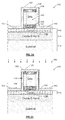
- the figure 1a is a sectional view of an example of this type of transistor 100 in progress. It contains the source and drain areas 110, generally designated source / drain zones, since they are very generally perfectly symmetrical and can play both roles depending on the electric polarizations that are applied to the transistor.
- the grid conventionally consists of a stack of layers 120, a large part of which is always composed of polycrystalline silicon 123.
- the formation of the source and drain zones is typically done by ion implantation 105 of dopants in the zones 110, the grid 120 serving mask as mentioned above, thus preventing the doping of the area of the MOSFET transistor in which, depending on the voltages applied to the gate, will be able to develop the channel 130 of conduction between source and drain.
- a widely used technique currently consists in manufacturing the integrated circuits starting from elaborate substrates 140 of silicon-on-insulator type, designated by their acronym SOI, of the English "silicon on insulator".
- SOI silicon-on-insulator type
- the SOI developed substrate is characterized by the presence of a thin superficial layer of monocrystalline silicon 146 resting on a continuous layer of silicon oxide 144, called buried oxide or BOX, acronym for "buried oxide layer”.
- BOX buried oxide layer
- the strength and the mechanical rigidity of the assembly are ensured by the layer 142 which constitutes the body of the SOI substrate, often described as "bulk” to indicate that the starting substrate is very generally made of solid silicon.
- This structure offers many advantages for the realization of MOSFET transistors. In particular, it allows a drastic reduction of parasitic capacitances due to the presence of the insulating continuous layer 144.
- the surface layer of monocrystalline silicon 146 can be precisely controlled in thickness and in doping .
- the channel 130 can be completely deserted carriers, that is to say “fully depleted” (FD), English term which is generally used to designate this state. This is achieved by producing the transistors from SOI substrates whose surface layer 146 is very thin, which is not without disadvantage otherwise as will be seen in the description of the invention. This type of transistor is thus designated by the acronym FDSOI.
- spacers 150 on the flanks of the grid.
- the spacers 150 typically made of silicon nitride (SiN), will allow in particular the implementation of a technique called “Source and Drain elevated”.
- Source and Drain elevated In order to maintain low electrical resistance to access the source and drain electrodes, despite the size reduction of the transistors, it was indeed necessary to increase their section. This is obtained by selective epitaxy of the source / drain zones 110. During this operation, the initial layer of monocrystalline silicon 14 will be grown locally 112. It is then necessary to protect the grid areas to prevent the growth from also being made from polycrystalline silicon 123 of the grid. It is, among other things, the role of spacers to ensure this function. They also perform a role of preserving the gate during siliciding of the contacts (not shown) which is then performed for the same purpose in order to reduce the series resistance of access to the electrodes of the transistor.
- the spacers are made without involving any photoengraving operation. They are self-aligned on the gate 120 from the deposition of a uniform layer of silicon nitride 152 (SiN) which then undergoes a very strongly anisotropic etching. This etching of the SiN preferentially attacks the horizontal surfaces, that is to say all the surfaces that are parallel to the plane of the SOI substrate. It leaves in place, imperfectly, only the vertical portions of the layer 152, those substantially perpendicular to the plane of the substrate, in order to obtain in practice the patterns 150 whose ideal shape would obviously be rectangular.
- the figures 1b , 1c and 1d each illustrate a type of defect observed.
- etching is used which is said to be “dry” and which is carried out using a process which is most often referred to by its acronym RIE, of the English “reactive-ion eching", c. 'ie reactive ion etching'. It is an etching process in which a plasma is formed in a confined space that reacts physically and chemically with the surface of the wafer to be etched.
- the reactive gas is typically methyl fluoride (CH 3 F) which is reacted. with the material to be etched by also introducing oxygen (O2).
- etching plasma based on fluorine chemistry is thus formed and often designated by its constituents: CH3F / O2 / He.
- the fluorine compound serves to etch the silicon nitride whereas the oxygen makes it possible to limit the polymerization of the methyl fluoride and also serves to oxidize the silicon when this material is reached during etching.
- the oxide layer formed on the silicon makes it possible to slow the etching of the silicon at the cost, however, of a surface conversion of the latter into oxide and thus of a silicon surface consumption.
- Helium serves as a diluent for oxygen.
- the advantage of this type of etching is that it is fairly anisotropic and allows to control sufficiently the profile of the spacers 150 even if one can not obtain in practice the ideal rectangular shape.
- the disadvantage of this type of etching is that the etch selectivity of the underlying silicon is however limited.
- the selectivity that is to say the ratio of the etching rates between the silicon nitride and the silicon is of the order of 10 and can reach a maximum of 15 depending on the conditions of formation of the plasma (the nitride is etched 10 to 15 times faster than silicon).
- wet etchings based on hydrofluoric acid (HF) or phosphoric acid (H3PO4) which have a much better selectivity, respectively, with respect to silicon or its oxide (SiO2) but which do not however make it possible to control the profile of the spacers since the etching is essentially isotropic in this case. Note that this type of engraving is also called “wet cleaning” translation of the English “wet clean”.
- the figure 1b illustrates a first problem which is related to the insufficient etching selectivity which exists during dry etching of the CH3F / O2 / He type between the silicon nitride and the silicon of the surface layer 146.
- the result is that A significant fraction of the thin surface layer of monocrystalline silicon 146 of the SOI substrate can then be partially consumed 147 during the anisotropic etching of the nitride.
- the surface layer 146 is chosen to be thin in order to improve the electrical characteristics of the transistors. It is typically less than 10 nm. The remaining thickness 145 may be very small. Under these conditions the ion implantation 105 to form the source and drain zones 110 which will follow is likely to be very damaging for the remaining monocrystalline silicon.
- the implantation energy of the dopants may be sufficient to cause complete amorphization 149 of the single-crystal silicon, which will then in particular compromise the next epitaxial growth step 112 intended to form the raised source / drain.
- this last operation is made necessary because of the size reduction of the transistors in order to be able to maintain the access resistances to the source and drain electrodes at sufficiently low values so as not to impact the electrical operation of the transistors. Growth from a partially or totally amorphous silicon layer will create many defects in the layer formed by epitaxy.
- the figure 1c illustrates another problem where there is no significant silicon consumption of the surface layer 146 but there is formation of "feet" 154 at the bottom of the remaining silicon nitride patterns on the sides of the gate after etching.
- the consequence is that the transition 114 of the junctions which are formed after ion implantation doping 105 of the source and drain zones 110, with the zone of the channel 130, is much less abrupt than when the spacers do not have feet as represented in FIG. previous figures.
- the presence of feet 154 affects the electrical characteristics of the transistors.
- the figure 1d illustrates a third problem that occurs when etching produces excessive erosion of the spacers in the upper portions of the grids and exposes polysilicon 123 in these areas 156.
- the consequence is that the subsequent epitaxial growth 112 to form the sources / Elevated drain will also occur at these locations, as well as silicidation of parasitic contacts, which may cause short circuits between electrodes.
- the etching of the spacers requires that the etching time is adjusted to etch, for example, 150% of the deposited nitride thickness. That is, a 50% overgraft is performed in this example to account for the non-uniformity of the deposit, or the etching operation itself, at a wafer.
- This type of defect is also called "faceting".
- a protective layer often based on carbon such as a mask or a photoresist (or "photoresist") or heat-sensitive to protect during the etching of spacers structures formed on the substrate.
- a protective layer often based on carbon such as a mask or a photoresist (or "photoresist") or heat-sensitive to protect during the etching of spacers structures formed on the substrate.
- This is for example the case when producing PMOS transistors close to NMOS transistors whose spacers are in progress.
- the known methods of etching can lead to a high consumption of this protective layer during etching of the spacers of the PMOS transistor.
- the object of the present invention is to propose a method for forming spacers which fully plays their role of isolation and which would eliminate or limit at least some of the defects in the production of transistors, such as the consumption or the alteration of the semiconductor material.
- one aspect of the present invention relates to a method of forming the spacers of a gate of a field effect transistor, the gate being located above a layer of a semiconductor material, comprising a step of forming a dielectric layer covering the gate of the transistor.
- the method comprises, after the step of forming the dielectric layer, at least one step of modifying said dielectric layer by placing the dielectric layer in contact with a plasma comprising light ions.
- Plasma creates anisotropic light ion bombardment in a preferred direction parallel to flanks of the grid, the plasma conditions, in particular the light ion energy and the implanted dose being chosen so as to modify at least portions of the the dielectric layer which are located on a top of the gate and on either side of the gate and which are perpendicular to the sides of the gate while maintaining portions unmodified dielectric layer covering the sides of the grid; the light ions being ions based on hydrogen (H).
- the method also includes at least one step of removing the modified dielectric layer by selectively etching said layer-modified dielectric layer of a semiconductor material and against the unmodified dielectric layer.
- the step of modifying the dielectric layer is carried out by bringing the dielectric layer into contact with a plasma formed from a gaseous mixture formed of at least a first non-carbonated gaseous component whose dissociation generates said light ions and a second gaseous component comprising at least one species promoting the dissociation of the first component to form said light ions, wherein the ratio of gas between the first component and the second component is between 1: 19 and 19: 1.
- the step of modifying the dielectric layer is carried out in a plasma formed from a gaseous mixture formed of at least a first non-carbon gas whose dissociation generates said hydrogen-based ions (H) and a second gas comprising at least one species promoting dissociation of the first component to form said hydrogen-based ions (H), wherein the ratio of the first gas to the second gas is from 1: 19 to 19: 1.
- the role of the first component is to modify, by ion bombardment, the crystalline structure of the dielectric layer in order to subsequently be able to differentiate the initial dielectric layer from the modified dielectric layer.
- the problem is that if we use a plasma based on only one component, hydrogen (H 2 ), for example, the risk is not to uniformly modify the dielectric layer in its thickness. This results in poor control of the actual depth up to which the modified layer has significantly improved selectivity. In this case, the depth of the ion implantation in the dielectric layer is not equivalent to the thickness of the modified dielectric layer whose selectivity is significantly improved and which will be etched after the bombardment.
- a second component advantageously acting as a dissociation gas makes it possible to facilitate the dissociation of the first component and thereby promote implantation of said first dissociated component in the dielectric layer, in the form of light ions.
- the implanted dose is therefore higher without having to increase the maximum implantation depth. It is therefore important to find a fair ratio between the content of first component and second component in the plasma for modifying the dielectric layer.
- the ratio of gas between the first component and the second component is greater than 1:19 and less than 19: 1. A lower ratio, which would be the case if the flow rate of the first gas is reduced, would have the effect of limiting the efficiency of the modification of the dielectric film.
- said ratio is between 1: 19 and 19: 1.
- said ratio is between 1: 9 and 9: 1.
- said ratio is between 1: 5 and 5: 1.
- a ratio between two gaseous components is a ratio relating to the respective rates of introduction of the components into the chamber of the plasma, typically in the plasma reactor. Each flow is usually measured in sccm. Typically a flow rate is measured with a flow meter associated with the reactor.
- the skilled person would have at best increased the duration of implantation to try to increase the dose without increasing the implanted depth.
- increasing the implantation time is not a solution because it causes a constraint from an industrial point of view (a loss of time necessarily entailing significant costs).
- the skilled person would have increased the flow of light gas, the problem is that too much concentration of gas in the reactor would not result in a greater depth of implantation. In fact, beyond a certain proportion of the first gas in the plasma, this first gas no longer dissociates. The density of light ion ions in the plasma and thus the content of implanted ions no longer increase.
- the layer underlying the dielectric layer typically the active layer of semiconductor material is not impaired.
- the transistor performance is not degraded.
- implantation is performed from a plasma comprising said light ions.
- Plasma implantation has the advantage of allowing implantation to be continuous in a volume extending from the surface of the implanted layer.
- the use of plasma allows implantation at lower depths than the minimum depths that can be obtained with implants.
- a plasma implantation makes it possible to implement efficiently and relatively homogeneously or at least continuously thin layers that can then be removed by selective etching.
- This continuity of implantation from the implanted face makes it possible to improve the homogeneity of the modification according to the depth, which leads to a constant etching rate in the time of the implanted layer.
- the increase of the selectivity conferred by the implantation with respect to the other layers is effective from the beginning of the etching of the implanted layer. The plasma implantation thus allows a significantly improved control of the engraving accuracy.
- Plasma implantation typically allows implanting and then removing thicknesses extending from the surface of the implanted layer and at a depth of 0 nm to 100 nm.
- Traditional implanters allow implantation in a volume between 30 nm and several hundred nanometers.
- conventional implanters do not make it possible to implant the species between the surface of the layer to be implanted and a depth of 30 nm.
- the implanters do not then make it possible to obtain a sufficiently constant etching rate of the modified layer from the surface of the latter, thus leading to a lower precision of engraving compared to what the invention allows.
- a plasma to modify the layer to be removed is therefore particularly advantageous in the context of the invention which aims to remove a thin layer of a dielectric layer, typically between 1 and 10 nm and more generally between 1 and 10 nm. 30 nm.
- the modification step made from a plasma modifies the dielectric layer continuously from the surface of the dielectric layer and over a thickness of between 1 nm and 30 nm and preferably between 1 nm and 10 nm.
- the implantation and the removal of the dielectric layer are carried out in the same plasma reactor.
- a modification of the layer to be removed by plasma implantation thus makes it possible to modify the layer and etch it in the same chamber, which is very advantageous in terms of simplification, time and cost of the process.
- This implantation also means that the thickness of the modified dielectric layer is increased more rapidly than that of the unmodified dielectric layer.
- the invention is based in particular on the fact that the second component forming the plasma is able to act as a dissociation gas vis-à-vis the first component, preferably based on hydrogen.
- the density of hydrogen ions in the gas phase is increased.
- the density of hydrogen contained in the dielectric layer by using the method according to the present invention is greater than that obtained from a plasma containing only hydrogen (H2).
- the consumption of the modified dielectric layer by a hydrofluoric acid-based cleaning is close to the depth of the ion implantation in said modified dielectric layer.
- the depth of implantation in the dielectric layer it is possible to estimate with a better precision the thickness of the modified dielectric layer which will be etched after implantation.
- the present invention allows a better control of the modification of the dielectric layer and in particular a better estimation of the thickness of the modified dielectric layer, which can be differentiated more strongly from the initial dielectric layer, thanks to a stronger a dose of hydrogen-based light ions implanted in said dielectric layer.
- the method according to the present invention proposes a reduction of the ionic energy for a similar thickness of the dielectric layer, allowing, in a particularly advantageous manner, to reduce the faceting of the hard mask as well as the damage that can be generated on the stack Si / SiGe.
- the modification of the dielectric layer is carried out using a carbon-free chemistry so as to avoid the formation of a residual layer based on carbon which would make it difficult to etch the dielectric layer.
- Etching consumes the modified dielectric layer preferentially to the layer of a semiconductor material and the unmodified dielectric layer. Thus, the risk of excessive consumption of the surface layer of semiconductor material is reduced or eliminated.
- the modification of the dielectric layer maintains an unmodified dielectric thickness on the sidewalls of the gate. This thickness is preserved, at least in part, during the selective etching. It then defines grid spacers.
- the invention thus makes it possible to obtain spacers based on a dielectric material while reducing or even eliminating the problems of the solutions known and mentioned previously.
- the invention is particularly advantageous for the formation of spacers of FDSOI transistors for example.
- the modification of the dielectric layer by implantation of light ions such as hydrogen (H2) also makes it possible to improve the selectivity of this modified dielectric layer with respect to the oxide of the layer in a semi-solid material. -driver.
- the method may further have at least any of the features and steps below.
- the implantation parameters in particular the implantation energy of the light ions from the first component and the implanted dose, are provided so that the modified dielectric layer can be etched selectively with respect to said implanted dose. semiconductor material and vis-à-vis the unmodified dielectric layer.
- the etching of the dielectric layer is carried out using a carbon-free chemistry.
- a carbon-free chemistry advantageously avoids the deposition of a carbonaceous layer that can hinder the etching of the dielectric layer.
- the role of the first component is to modify, by ion bombardment, the crystalline structure of the dielectric layer in order to subsequently be able to differentiate the initial dielectric layer from the modified dielectric layer.
- H 2 hydrogen
- the depth of the ion implantation in the dielectric layer is not equivalent to the thickness of the modified dielectric layer which will be etched after the bombardment.
- the implanted dose of hydrogen is not sufficient then this also causes nonuniformity of the implanted species in the dielectric layer, thereby causing poor control of the actual depth of the modified dielectric layer.
- a second component advantageously acting as a dissociation gas such as argon, helium, xenon, nitrogen
- the ratio of gas between the first component and the second component is greater than 1: 9 and less than 9: 1.
- the first component is selected from hydrogen (H2), silicon nitride (SiH4), hydrogen nitride (NH3) or hydrogen bromide (HBr).
- the second component is chosen from helium (He), nitrogen (N2), argon (Ar) or xenon (Xe).
- the entire dielectric layer located on the top of the gate and on either side of the gate is modified.
- the dielectric layer located on the sidewalls of the gate is not modified.
- the entire dielectric layer located on the top of the gate and on either side of the gate is removed by etching.
- the dielectric layer is formed of one or more dielectric materials whose dielectric constant k is less than or equal to 8 and preferably less than or equal to 7.
- the present invention is not limited to one layer. formed dielectric based on nitride.
- the present invention is also not limited to a dielectric layer of silicon nitride (SiN).
- the present invention advantageously extends to any spacer comprising a low k (low-k) dielectric material in which, according to one embodiment, the dielectric layer comprises a material having a dielectric constant of less than 4 and preferably less than 3.1 and preferably less than or equal to 2.
- the dielectric layer is advantageously a silicon-based layer (Si).
- the material of the dielectric layer is preferably selected from: SiCO, SiC, SiCN, SiOCN, SiCBN, SiOCH, CBN, BN, and SiO 2.
- the dielectric layer is a non-porous layer.
- the dielectric layer is a porous layer.
- the term porous layer a layer whose presence of vacuum in the film is greater than 5% and preferably between 5 and 10%.
- the dielectric layer is made of silicon nitride and the step of forming the dielectric layer comprises a step of depositing the dielectric layer during which is carried out followed by a step of reducing the dielectric constant of the dielectric layer.
- the step of reducing the dielectric constant of the dielectric layer comprises introducing a porosity into the dielectric layer.
- the dielectric layer is made of silicon nitride and the layer forming step dielectric comprises the introduction of precursors into the dielectric layer being deposited deposition precursor formation.
- the dielectric layer is a layer based on silicon nitride and the precursors are chosen so as to form bonds reducing the polarizability of the dielectric layer. These precursors are chosen so as to generate less polar bonds than silicon nitride, such as Si-F, SiOF, Si-O, C-C, C-H, and Si-CH3.
- the step of modifying the dielectric layer modifies the dielectric layer continuously from the surface of the dielectric layer and over a thickness of between 1 nm (nm) and 30 nm, preferably between 1 nm and 10 nm.
- the flow rate of the first component is between 10 and 1000 sccm (cubic centimeter per minute).
- the flow rate of the second component is between 10 and 1000 sccm.
- the step of modifying the dielectric layer is performed so as to provide a polarization power or source power, at a frequency of between 100 Hz (Hertz) and 5 kHz, with a duty cycle of between 10% and 90%. %.
- the modification step comprises bringing the dielectric layer into contact with a plasma comprising the light ions in an etching reactor.
- light ions means ions from materials whose atomic number in the periodic table of elements is low. In a general way all the elements that can be implanted in the material to be engraved, without causing dislocation of its atomic structure such that it would result in a spraying of the latter, and therefore without re-deposition of the material etched on the reactor walls or the patterns being etched themselves, are likely to agree.
- the light ions are taken from hydrogen (H2).
- the step of removing the modified dielectric layer is carried out by selective wet etching at the layer of a semiconductor material.
- the semiconductor material is silicon and the step of removing the modified dielectric layer is carried out by selectively wet etching with silicon (Si) and / or with silicon oxide (SiO 2).
- the selective silicon etching is obtained using a solution based on hydrofluoric acid (HF) or using a phosphoric acid solution (H3PO4) for a dielectric layer based on silicon nitride (SiN).
- the removal step is performed by selective dry etching at the layer of a semiconductor material.
- the layer made of a semiconductor material is silicon.
- the step of removing the modified dielectric layer is carried out by selective dry etching with silicon (Si) and / or with silicon oxide (SiO 2).
- the dry etching is carried out in a plasma formed in a confined chamber from a mixture of nitrogen trifluoride (NF3), hydrogen (H2) or ammonia (NH3) to form hydrofluoric acid (HF).
- NF3 nitrogen trifluoride
- H2 hydrogen
- NH3 ammonia
- the dry etching comprises: an etching step consisting of the formation of solid salts; a step of sublimation of the solid species.
- This embodiment makes it possible to obtain a very good selectivity of the etching of the modified dielectric layer with respect to the unmodified dielectric layer and to the unmodified semiconductor material.
- this selectivity of the etching is much greater (typically a factor of at least 10) than that obtained with a solution of HF.
- a single modification step is performed so as to modify the dielectric layer throughout its thickness on all the surfaces parallel to the plane of a substrate on which the grid rests and not to modify the dielectric layer throughout its thickness on the surfaces parallel to the preferred direction of the bombing.
- the light ions comprise ions based on hydrogen (H2) taken from: H, H +, H2 +, H3 +.
- the light ions comprise ions based on hydrogen (H2) taken from H, H +, H2 +, H3 +
- the implantation is performed so as to modify the entire thickness of the dielectric layer outside the dielectric layer disposed on the sides of the grid.
- etching removes the entire dielectric layer with the exception of at least a portion of the dielectric layer located on the sidewalls of the grid.
- the thickness of the modified dielectric layer on the sidewalls of the gate is zero or less than the thickness of the dielectric layer before modification by implantation.
- the implantation modifies the dielectric layer from its surface and to depth corresponding to at least part of its thickness.
- the implantation modifies the dielectric layer uninterruptedly from the surface.
- the method comprises a single modification step performed so as to modify the dielectric layer throughout its thickness on all the surfaces parallel to the plane of a substrate on which the grid rests and not to modify the layer. dielectric throughout its thickness on surfaces perpendicular to this plane. These surfaces perpendicular to this plane, that is to say perpendicular to the layer of a semiconductor material forming a conduction channel or solid substrate are typically parallel to the sides of the gate of the transistor.
- a selective etching of the modified dielectric layer makes it possible to remove the dielectric layer on all the surfaces except on those parallel to the sidewalls of the gate.
- the method comprises several sequences each comprising a modification step and a withdrawal step.
- a modification step During at least one of the modifying steps, only a portion of the thickness of the dielectric layer is changed.
- the sequences are repeated until the dielectric layer disappears on all the surfaces parallel to the plane of a substrate on which the grid rests. Only the faces parallel to the sidewalls of the grid retain a dielectric thickness, this thickness has not been modified by implantation.
- the dielectric layer is disposed directly in contact with the layer of a semiconductor material.
- the dielectric layer is disposed directly in contact with the gate which is preferably formed of a semiconductor material.
- the gate of the transistor is located on a stack of layers forming an elaborate silicon-on-insulator (SOI) substrate. Preferably, it is disposed directly in contact with the layer forming the conduction channel.
- SOI silicon-on-insulator
- the use of the invention with such an SOI substrate makes it possible to preserve the integrity of the superficial layer of very thin thickness which forms the conduction channel of a transistor formed from an SOI substrate.
- the semiconductor material is silicon.
- the etching is selective for silicon oxide (SiO 2).
- the semiconductor material may also be germanium (Ge) or silicon-germanium SiGe.
- the step of removing the modified dielectric layer is carried out by selectively etching with Ge or SiGe or and / or with SiGe oxide or Ge oxide.
- the transistor is a FDSOI type transistor.
- the method comprises a step of completely removing the dielectric layer outside the sidewalls and on both sides of the grid to expose the layer in a semiconductor material and a source zone forming step drain from the layer into a semiconductor material, for example by epitaxy.
- the implantation in particular its energy, the concentration and the nature of the light ions, the dose used and the duration of the implantation process, are provided so that the modified dielectric layer can be etched selectively vis-à- screw the remainder of the dielectric layer, that is to say the unmodified dielectric layer.
- the modification of the silicon dielectric layer by implantation of hydrogen (H2) makes it possible to improve the selectivity of this layer with respect to silicon and / or silicon oxide.
- the etching is obtained, for example, using a solution based on phosphoric acid (H 3 PO 4) for a dielectric layer 152 based on silicon nitride or using a solution based on of hydrofluoric acid (HF).
- H 3 PO 4 phosphoric acid
- HF hydrofluoric acid
- the term “over”, “overcomes” or “underlying” or their equivalent do not necessarily mean “in contact with”.
- the deposition of a first layer on a second layer does not necessarily mean that the two layers are in direct contact with one another, but that means that the first layer at least partially covers the second layer. being either directly in contact with it or separated from it by another layer or another element.
- the thicknesses are generally measured in directions perpendicular to the plane of the lower face of the layer to be etched or a substrate on which the lower layer is disposed. Thus, the thicknesses are generally taken in a vertical direction in the figures shown. On the other hand, the thickness of a layer covering a flank of a pattern is taken in a direction perpendicular to this flank.
- FIGS. 2a to 2d describe the steps of a detailed example of a method according to the invention applied to the realization of FDSOI type transistors.
- the principles of these steps can also be applied to the formation of spacers on the flanks of a gate of another type of transistor.
- the figure 2a illustrates the step of depositing a dielectric layer 152, preferably of substantially uniform thickness, on all the vertical and horizontal surfaces of the devices being manufactured.
- This step is preferably carried out using a so-called LPCVD deposition method, ie “low pressure chemical vapor deposition", that is to say “low pressure chemical vapor deposition” .
- LPCVD deposition method ie “low pressure chemical vapor deposition”
- This type of deposit which is practiced under atmospheric pressure allows indeed a uniform deposit on all surfaces regardless of their orientation.
- the gate electrode is composed at this stage of the multi-layer method for certain types of transistors.
- the polycrystalline silicon layer 123 there are found in the stack layers forming the gate 120 firstly the thin insulating layer of gate oxide 121 through which an electric field will be able to develop to create the channel 130 of underlying conduction between source and drain when a voltage sufficient is applied on the grid.
- a high-k / metal gate technology is used which is to say that the insulating layer 121 is made of an insulating material with a high permittivity ( high-k) covered by a metal gate represented by the layer 122.
- the stack of layers of the grid also comprises a hard mask 124 of protection which will be removed later to allow the resumption of contact on this electrode.
- This hard mask which remains in place after etching the gate, is typically made of silicon oxide (SiO2). Its role is to protect the top of the grid from any damage during the engraving of the spacers.
- the insulating layer 121 is disposed in contact with the layer 146 of a semiconductor material forming the conduction channel.
- the layer 122 is disposed in contact with the layer 121.
- the layer 123 is disposed directly in contact with the gate oxide formed by the layer 121, if the layer 122 is absent or is disposed directly in contact of the layer 122.
- the dielectric layer 152 is disposed directly in contact with the layer 123 at the sidewalls of the gate.
- the dielectric layer 152 is disposed directly in contact with the layer 146 of a semiconductor material for forming the conduction channel.
- the dielectric layer 152 is based on nitride.
- the nitride dielectric layer 152 has a thickness of between 5 and 20 nm, and typically of the order of 10 nm.
- the dielectric layer 152 is based on silicon nitride (SiN).
- the dielectric layer 152 comprises a low k (or low dielectric constant k) dielectric material, with k preferably less than or equal to 7.
- the present invention is not limited to dielectric layer formed based on nitride.
- the present invention is also not limited to a dielectric layer of silicon nitride (SiN).
- the present invention advantageously extends to any spacer comprising a dielectric material with low permittivity k (called "low-k” in English).
- the permittivity of a material is a tensor magnitude (the response of the material may depend on the orientation of the axes crystallographic material), which is reduced to a scalar in isotropic media.
- the dielectric constant is denoted k in the field of integrated circuits and semiconductors, for example.
- the so-called "low-k” materials are dielectrics with low permittivity. They are used as insulators between metal interconnects to reduce the coupling between them.
- the dielectric layer 152 has or comprises a material having a dielectric constant of less than 4 and preferably less than 3.1 and preferably less than or equal to 2, thereby reducing the parasitic capacitance to possibly improve the transistor performance.
- the material of the dielectric layer 152 is taken from: SiCO, SiC, SiCN, SiOCN, SiCBN, SiOCH and SiO2. This reduces the parasitic capacitance and consequently improves the performance of the transistor.
- the method of the invention comprises an optional step of reducing the dielectric constant of the dielectric layer 152.
- the reduction of the dielectric constant is obtained during the step of depositing the dielectric layer 152.
- the reduction of the dielectric constant comprises the introduction into the dielectric layer 152 in forming precursors which form bonds reducing the polarizability of the dielectric layer 152.
- precursors are chosen so as to generate less polar bonds as silicon nitride, such as Si-F, SiOF, Si-O, CC, CH, and Si-CH3.
- the reduction of the dielectric constant comprises the introduction into the dielectric layer 152 forming a porosity.
- the figure 2b illustrates the next step of the invention applied to the realization of FDSOI transistors in which a modification 430 of the dielectric layer 152 that has just been deposited is directly carried out.
- this operation may have been preceded by a conventional dry etching type CH3F / O2 / He.
- the modification step 430 of the dielectric layer 152 as deposited, or of the layer remaining after a first conventional etching, is by implantation 351 of light species also designated light ions.
- these ions are ions based on hydrogen (H). These ions can be implanted in a material to be etched, without causing dislocation of its atomic structure such that it would cause a spray of the latter.
- the modification of the dielectric layer 152 to be etched is based on the implantation of light species based on hydrogen (H) such as: H, H +, H2 +, H3 +.
- the implantation of light species is favored by the incorporation into the plasma of a second component allowing the dissociation of the light ions and therefore the increase in the density of light ions in the plasma and the plasma. increase of the implanted dose.
- the implantation parameters in particular the energy imparted to the ions, the duration and the implantation dose are provided so that the modified dielectric layer 158 can be etched selectively with respect to the layer 146 in a semiconductor material. driver.
- these parameters are also adjusted so that the modified dielectric layer 158 can be etched selectively with respect to the unmodified portion of the dielectric layer 152.
- these parameters are also adjusted so that the modified dielectric layer 158 can be etched selectively with respect to a layer made of an oxide, typically an oxide of said semiconductor material, the latter forming for example an oxide layer grid.
- the etching is selective of the modified dielectric material by implantation of hydrogen vis-à-vis the silicon oxide.
- Implantation is effected for example in a plasma based on hydrogen gas (H2). More generally, all the gaseous components, which can dissociate the light ions mentioned above, can be used in the plasma. It will be noted here that this modification step 430 of the dielectric layer 152 to be etched can be practiced in many different ways by adapting all kinds of means commonly used by the microelectronics industry. In particular, standard etching reactors are used in which low or high density plasmas can be produced and where the energy of the ions can be controlled to allow the implantation of the light species above intended to modify the layer to be etched. It is also possible to use a type of so-called immersion plasma commonly used for practicing implantation of species on the surface of a device during manufacture. Finally, implantation can also be done in a standard implanter where the ions are accelerated in an electric field to obtain their implantation in a solid.
- H2 hydrogen gas
- the modification operation is advantageously very anisotropic for the production of the spacers on the sidewalls of the grids because of the directionality of the ions of the plasma or the implanter. It therefore preferably affects the horizontal surfaces, that is to say all the surfaces parallel to the plane of the substrate 142.
- the thickness modified on the horizontal surfaces 154 is thus much larger than on the vertical surfaces 156 that is to say on all surfaces perpendicular to the plane of the substrate 146 developed, on which is arranged the grid. This plane is perpendicular to the plane of the section represented on the Figures 2a to 2d .
- the prepared substrate 142 preferably forms a plate with two parallel faces. It is for example in the form of a disk, a square, a polygon, etc.
- the thin layer 146, the buried oxide layer 144 and the solid substrate 142 are arranged in parallel planes.
- a surface will be described as horizontal if it is parallel to the plane of the layer or layers forming the substrate 146, on which the grid is formed and a surface will be described as vertical if it is perpendicular to the same plane.
- a thickness 154 of 10 nm on the horizontal surfaces can be changed during this operation.
- a thickness 156 of the layer 152 ranging from 1 to 3 nm is however also modified on the vertical surfaces regardless of the plasma conditions. These vertical surfaces with respect to the plane of the substrate 146 are therefore parallel to the sides of the grid.
- the modified thicknesses depend on the conditions of implementation, in particular on the means employed (plasma or implanter) and also on the fact that it is desired to obtain the etching of the spacers in a single overall modification and etching step or that on the contrary repeat these operations until you obtain a complete engraving.
- the step of modifying this layer can affect the whole of this layer where, as represented in the example of the figure 2b , only part of it.
- the modification step 430 and the subsequent step 440 of removing the modified layer described below can be repeated until complete removal of the dielectric material of the modified dielectric layer 158 on all horizontal surfaces.
- the Figure 2c illustrates the final result of the next step after the etching process, that is to say the removal of the modified dielectric layer 158 and possibly repeated, on the one hand, the modification operation described in FIG. preceding, and secondly, the operation of removing the modified dielectric layer 158.
- One method used for the removal of the modified dielectric layer 158 is, as already mentioned, to use an etching solution, for example, based on hydrofluoric acid (HF) (or phosphoric acid (H3PO4) for a dielectric layer 152 based on silicon nitride). Stopping the etching is done on the unmodified dielectric layer 152 or on the monocrystalline silicon of the layer 146 or on the hard mask 124 at the top of the grids. It will be noted here, with reference to the problem described in figure 1b that there is no silicon consumption due to the use of hydrofluoric acid or phosphoric acid.
- HF hydrofluoric acid
- H3PO4 phosphoric acid
- an optimization of the modification step 430 by implantation of light species described above entails only a modification of the dielectric layer 152 and the subsequent etching operation does not therefore affect the silicon under -jacent.
- the vertical dielectric units remain essentially of the initial dielectric layer 152, essentially on the sidewalls of the stack of layers forming the gate 120. They constitute the gate spacers 150 of the transistor.
- the figure 2d illustrates the formation of the drain and source zones of a FDSOI type transistor.
- wet cleaning most often qualified by its English term wet clean
- the doping which will delimit the source and the drain and therefore the length of the channel 132 can be done by ion implantation before the epitaxially grow on these areas in order to increase their cross-section and decrease their resistance. If the doping is carried out before epitaxial growth, as shown on the figure 2d , the method is said to be an English term "first extension” used to indicate that the extensions (of source and of drain under the spacers) are carried out first, that is to say before epitaxial growth. Otherwise, who is said to be "extension last", proceed directly to the epitaxial growth step without prior doping. The doping of the source / drain zones is done only after epitaxial growth of these zones.
- the implanted dopants are typically arsenic (As) or phosphorus (P).
- the dopants are boron (B) or boron difluoride (BF2).
- the figure 3 illustrates the ion implantation profiles obtained for different species (Argon, Helium, Hydrogen) in a silicon nitride layer with an energy of 300 eV.
- the ions (argon, helium, hydrogen, hydrogen associated with another component), having a kinetic energy of 300 eV, reach the surface of the plate (corresponding to the DC bias, measured at the surface of the plate (-300 V)).
- the simulated Rp profile, illustrated in figure 3 is estimated between 2 nm, 7 nm and 12 nm using, respectively, a plasma based on argon 510, helium and hydrogen 530.
- the consumption of the silicon nitride layer is estimated at 2 nm.min -1 under the experimental conditions of this example. Therefore, the degradation of the SiN layer, generated by the ions, is suppressed because formed by the rate of argon sputtering.
- the ion implantation is deeper. Thus, the degraded modified layer can be adjusted, taking into account the consumption of said layer.
- a hydrogen-based plasma 530 does not etch the silicon nitride layer. Therefore, the use of a hydrogen plasma offers a larger process window than helium, allowing more precise and controlled modification of the depth of the modified silicon nitride layer. Based on these results, it appears that a plasma preferably based on hydrogen offers a particularly interesting means for precise control of the etching depth.
- HF hydrofluoric acid
- the Figures 4a, 4b and 4c illustrate an embodiment according to the prior art where a dielectric layer 152, formed on a substrate 142, is modified and then removed by plasma etching based on hydrogen only.
- the Figures 5a, 5b and 5c illustrates an embodiment according to the invention wherein a dielectric layer 152, formed on a substrate 142, is modified and then removed by hydrogen-based plasma etching associated with another component X, acting as a dissociation gas.
- the dopant of the present invention it has been observed that there is a threshold value of the hydrogen dose from which the dielectric layer 152 is sufficiently modified to be attacked by means of a dye-based cleaning.
- hydrofluoric acid for example, or at least to be etched with a high selectivity to the unmodified material of the dielectric layer 152. If the material of the dielectric layer 152 is modified without the dose being less than this threshold dose, then the modified material of the dielectric layer 152 will not be etched or will be etched with a low selectivity vis-à-vis the unmodified material.
- the known solutions do not make it possible to reach this threshold dose for the maximum implanted depth. Indeed, above the depth at which the threshold dose is reached, there is a depth of about 3 to 5 nm, which is implanted but without presenting an implanted dose equal to or greater than the threshold dose.
- the dielectric layer 152 in this example formed based on silicon nitride, is implanted by light ions H, for example.
- the modified dielectric layer 158 is not uniformly implanted over the entire maximum depth Pmax of the dielectric layer 152.
- only a portion of the dielectric layer 152, on a Threshold depth Ps is implanted with a dose greater than or equal to the threshold dose sufficient to allow selective etching of the modified dielectric layer 158.
- One way to increase the H dose of ions in the silicon nitride layer is to increase the treatment time.
- the problem is the time consuming (> 600 s) important to saturate the hydrogen in the SiN layer.
- This solution because of the important time it requires, can not therefore be implemented from an industrial point of view (high cycle time, today the treatment time for etching a nitride spacer being less than 60 s).
- a problem to be solved is the removal of the modified layer, since the modified layer is removed by HF cleaning from only a light ion dose threshold value implanted in the nitride layer. As a result, the damage caused in the nitride layer by the HF cleaning is underestimated. Thus, if we target a 15nm thickness removal of silicon nitride layer thickness by 1% HF cleaning, the risk is to damage the underlying layer (Si or SiGe), since the depth of ion implantation will be deeper than 15 nm.
- the present invention allows a better control of the modification of the dielectric layer 152 (thanks to a higher dose of H implanted in the SiN layer) and thus by a reduction of the energy of the ions (reduction of the damage which can affect the Si / SiGe underlying layers).
- the Figures 5a to 5c illustrate an embodiment according to the present invention wherein the method makes it possible to modify the dielectric layer 152 so that the modified dielectric layer 158 is implanted on the depth Pmax with a dose greater than the threshold dose, thus allowing precise etching the modified dielectric layer 158 over the entire depth Pmax.
- the use of a second component acting as a dissociation gas X (with X chosen for example from: Ar, He, Xe, N2) with the chemistry of the first component H2, advantageously makes it possible to increase the concentration of light ions in the gas phase. Therefore, for the same implantation energy, the dose H implanted in the SiN layer is greater than that obtained from a plasma based on a single component H2 only.
- the profile Rp (associated with the implantation depth) for implantation from a plasma based on a gas comprising at least a first non-carbonaceous gaseous component (H2) and a second component (X with X selected, for example among: Ar, He, Xe, N2) dissociation gas is close to that obtained for an implantation based on a single component H (cf. figure 3 ). Only the implanted dose will be greater in the case of a plasma comprising a first component H and a second component X compared to a plasma comprising only hydrogen, for example. In this way, the threshold dose of implantation can be reached at the maximum depth Pmax at which the light ions are implanted.
- the consumption of the modified dielectric layer 158 by the HF cleaning is close to the implantation depth Pmax of the ions.
- a better accuracy is obtained for etching the dielectric layer 152, without, however, damaging the underlying layer.
- the figure 6 summarizes the steps of the process of the invention intended to form spacers and which do not induce any of the defects described in particular in the Figures 1b, 1c and 1d for producing transistors, for example FDSOI.
- the said modified dielectric layer 158 is removed on the surfaces that are not intended to be used. form the spacers. This removal comprises several steps, including steps 430, 440 and optionally step 420 beforehand.
- anisotropic conventional dry etching 420 is carried out of the modified dielectric layer 158. This is typically carried out in a CH3F / O2 / He type plasma described above.
- the etching of the spacers is thus, according to this optional and nonlimiting embodiment, carried out in two steps comprising: a first step called “main etching” and a second finishing step generally described as “over-etching” or the English-speaking term of "over etching (OE)" having the same meaning.
- step 440 the dielectric material of the modified dielectric layer 158 remaining on the horizontal surfaces will be removed after having modified (step 430) the dielectric layer 152 to avoid or limit the problems described in the Figures 1b to 1d .
- next step 430 consists in anisotropically modifying all or part 154 of the remaining dielectric layer 152 by implantation of light ions.
- the second component interacts with the first component to dissociate the first component and promote the creation of light ions, thereby increasing the concentration of H ions and the dose.
- the cost of the apparatus is lower, the manufacturing cycle times may be shorter since the main etching step 420 and that of modification 430 of the dielectric layer 152 can then be done in the same apparatus without releasing devices in the process of manufacture.
- modification step 430 can be practiced in many different ways by adapting all kinds of means commonly used by the microelectronics industry, such as using any type of burner, for example in a ICP reactor of the English “Inductively Coupled Plasma” that is to say “inductively coupled plasma”, or in a type of reactor CCP of the English “Capacitive Coupled Plasma” that is to say “plasma Capacitive coupling "which controls the energy of the ions.
- a type of plasma called immersion commonly used to practice a species implantation on the surface of a device during manufacture.
- the person skilled in the art in order to determine the behavior of the material to be etched in the type of plasma etcher chosen, will preferentially proceed to "full-plate” tests in order to establish behavior curves. He will deduce the parameters of the implantation, in particular the energy and the dose of ions, that is to say the exposure time, to use to reach the desired thickness of material to be modified.
- the next step 440 is that in which etching of the modified layer or at least the modified thickness of the modified dielectric layer 158 is practiced by etching.
- etching of the modified dielectric layer 158 is as selective as possible with respect to the silicon in particular so as not to attack the monocrystalline silicon of the source / drain zones with the disadvantages and consequences described above.
- a wet etching for example, based on hydrofluoric acid (HF) (or phosphoric acid (H3PO4) for a dielectric layer 152 based on silicon nitride) which, as already mentioned, combines the removal of the modified dielectric layer 158 with cleaning of the wafer containing the devices being manufactured, is advantageously used. This simplifies the process and saves time.
- HF hydrofluoric acid
- H3PO4 phosphoric acid
- the thickness of the modified dielectric layer 158 is typically in a range of values from 1 nm to a few tens of nm. Burning times can range from seconds to minutes. They are obviously directly dependent on the thickness that has been modified. For example, to remove a thickness of 15 nm from the modified dielectric layer 158, it takes about 60 seconds with a 1% solution of hydrofluoric acid (HF). An etching time of the order of 45 seconds is required with phosphoric acid (H3PO4).
- HF hydrofluoric acid
- H3PO4 phosphoric acid
- the etching of the modified dielectric layer 158 will also be as selective with respect to the silicon oxide in other applications of the method as that used for making the spacers of FDSOI type transistors where this is not useful. This is particularly the case for making three-dimensional transistors FinFET type. Selective dry etching with silicon and its oxide (Si / SiO2) can then also be practiced for this step of removing the modified dielectric layer 158.
- An alternative is therefore to perform a step of dry removal of the dielectric layer which has been modified 158 by implantation, preferably hydrogen.
- modified dielectric layer 158 The principle of dry removal of the modified dielectric layer 158 is identical to that described in the above publication. The difference is that, in the case of the invention, silicon oxide is not etched but a modified dielectric layer 158 having undergone implantation based on hydrogen. The mechanism is however the same and comprises the following steps which take place in a reaction chamber where a plasma is formed, that is to say in a plasma reactor.
- the thicknesses treated are typically between 1 nm and a few tens of nanometers.
- a first step 610 consists in generating the etching product in the plasma according to the following chemical reaction: NF 3 + NH 3 ⁇ NH 4 F + NH 4 F.HF which reacts nitrogen trifluoride (NF 3 ) with ammonia (NH 3 ) or with hydrogen (H2) to form hydrofluoric acid (HF).
- NF 3 nitrogen trifluoride
- NH 3 ammonia
- H2 hydrogen
- Etching is carried out during a second step 620, at a temperature of the order of 30 ° C. and more generally between 10 ° C. and 50 ° C., in the form of a salt formation according to the following chemical reaction : NH 4 F or NH 4 F.HF + SiNH ⁇ (NH 4 ) 2SiF 6 (solid) + H 2 during an operation which lasts between a few seconds and a few minutes and which takes place under a pressure of between a few milli Torr and a few Torr. More precisely, this operation lasts between 20 seconds and 2 minutes and is carried out under a pressure of between 500 milli Torr and 3 Torr.
- the streams of nitrogen trifluoride (NF 3 ) and ammonia (NH 3 ) are respectively 50 sccm and 300 sccm at 30 ° C for 45 seconds for step 620 salt formation which is followed by the sublimation step 630 which is carried out at 180 ° C for 60 seconds.
- This embodiment makes it possible to obtain a very good selectivity of the etching of the modified nitride relative to the unmodified nitride and to the unmodified semiconductor material.
- this selectivity of the etching is much greater (typically a factor of at least 10) than that obtained with a solution of HF.
- etching reactors for performing implantation for example of hydrogen, from a plasma which can be followed, in the same system, by removing the modified dielectric layer 158 from the plasma. using a dry etching as described above.
- etching reactors for performing implantation for example of hydrogen
- a plasma which can be followed, in the same system, by removing the modified dielectric layer 158 from the plasma. using a dry etching as described above.
- the modification operations 430 of the dielectric layer 152 and the recess 440 of the modified dielectric layer 158 may optionally be repeated 450 until the dielectric material of the modified dielectric layer 158 disappears on all the horizontal surfaces.
- step 430 of modifying the dielectric layer 152 in the case of using a standard plasma etching reactor. These conditions are largely dependent on the thickness to be modified in the dielectric layer 152. This is only a particular example of the implementation of step 430 for modifying the layer to be etched. As already mentioned, other means can be used for the implantation of the light species, H, used to modify the layer to be etched. In particular, it will be possible to use low or high density plasmas or plasmas by immersion.
- any type of dry etching device is potentially usable and especially those said ICP of the English “inductively coupled plasma” that is to say “inductively coupled plasma” or CCP of English “capacitively coupled plasma” that is to say “capacitively coupled plasma).
- These devices have the advantage of being able to achieve not only etchings, but also carbon deposits (C) in the same device.
- Engraving reactor The values below apply more particularly to the type of ICP burner although any type of dry etching device is potentially usable.
- Modified thickness from 1 nm to a few tens of nm, typically 15 nm
- a first hydrogen-based component H2, HBr, NH3, SiH4
- a second component gas permitting the dissociation of the first hydrogen-based ion component (H) selected from the group consisting of argon, nitrogen, xenon, helium.
- the figure 7 gives for the standard material used to form the spacers, that is to say the silicon nitride (SiN) in this example, the thicknesses of modified layers obtained according to different conditions of implementation of the step of implantation of light species in a standard plasma etching reactor.
- the figure 7 gives the modified thickness as a function of the bias voltage (bias) in volts for an ICP type burner and under the following conditions, for the figure 7 flow rate of the first component of 50 sccm; flow of the second sccm component; power of the source 500 watts; pressure 10 milli Torr.
- bias voltage bias voltage
- H2 hydrogen-based component
- He helium-based component
- N2 nitrogen
- Xe xenon
- Ar argon
- the dissociation of the first component by its interaction with the second component makes it possible to increase the concentration of hydrogen-based ions in the plasma, and therefore to increase the dose of implanted hydrogen.
- the hard mask faceting and damage are reduced. be generated on the Si / SiGe stack, compared to a hydrogen based plasma (H2) only.
- H2 hydrogen based plasma
Landscapes
- Engineering & Computer Science (AREA)
- Power Engineering (AREA)
- Microelectronics & Electronic Packaging (AREA)
- Physics & Mathematics (AREA)
- General Physics & Mathematics (AREA)
- Computer Hardware Design (AREA)
- Condensed Matter Physics & Semiconductors (AREA)
- Manufacturing & Machinery (AREA)
- Chemical & Material Sciences (AREA)
- Ceramic Engineering (AREA)
- Chemical Kinetics & Catalysis (AREA)
- General Chemical & Material Sciences (AREA)
- Inorganic Chemistry (AREA)
- Crystallography & Structural Chemistry (AREA)
- Plasma & Fusion (AREA)
- Insulated Gate Type Field-Effect Transistor (AREA)
- Thin Film Transistor (AREA)
Applications Claiming Priority (1)
| Application Number | Priority Date | Filing Date | Title |
|---|---|---|---|
| FR1555667A FR3037715B1 (fr) | 2015-06-19 | 2015-06-19 | Procede de formation des espaceurs d'une grille d'un transistor |
Publications (2)
| Publication Number | Publication Date |
|---|---|
| EP3107125A1 true EP3107125A1 (de) | 2016-12-21 |
| EP3107125B1 EP3107125B1 (de) | 2020-01-08 |
Family
ID=54478115
Family Applications (1)
| Application Number | Title | Priority Date | Filing Date |
|---|---|---|---|
| EP16174868.6A Active EP3107125B1 (de) | 2015-06-19 | 2016-06-16 | Verfahren zur bildung von abstandhaltern eines gates eines transistors |
Country Status (3)
| Country | Link |
|---|---|
| US (1) | US9947768B2 (de) |
| EP (1) | EP3107125B1 (de) |
| FR (1) | FR3037715B1 (de) |
Cited By (1)
| Publication number | Priority date | Publication date | Assignee | Title |
|---|---|---|---|---|
| FR3120157A1 (fr) * | 2021-02-25 | 2022-08-26 | Commissariat A L'energie Atomique Et Aux Energies Alternatives | Procédé de gravure d’une couche diélectrique tridimensionnelle |
Families Citing this family (7)
| Publication number | Priority date | Publication date | Assignee | Title |
|---|---|---|---|---|
| FR3051964B1 (fr) | 2016-05-27 | 2018-11-09 | Commissariat A L'energie Atomique Et Aux Energies Alternatives | Procede de formation d’un motif de guidage fonctionnalise pour un procede de grapho-epitaxie |
| FR3051965A1 (fr) | 2016-05-27 | 2017-12-01 | Commissariat Energie Atomique | Procede de formation d’un motif de guidage fonctionnalise pour un procede de grapho-epitaxie |
| FR3051966B1 (fr) | 2016-05-27 | 2018-11-09 | Commissariat A L'energie Atomique Et Aux Energies Alternatives | Procede de formation d’un motif de guidage fonctionnalise pour un procede de grapho-epitaxie |
| US11355340B2 (en) * | 2019-07-19 | 2022-06-07 | Iqe Plc | Semiconductor material having tunable permittivity and tunable thermal conductivity |
| FR3120156B1 (fr) * | 2021-02-25 | 2023-02-10 | Commissariat Energie Atomique | Procédé de gravure d’une couche diélectrique tridimensionnelle |
| FR3120158B1 (fr) | 2021-02-25 | 2023-04-14 | Commissariat Energie Atomique | Procédé de formation des espaceurs d'une grille d'un transistor |
| FR3122525B1 (fr) * | 2021-04-28 | 2024-01-19 | Commissariat Energie Atomique | Procédé de formation des espaceurs d'une grille d'un transistor |
Citations (6)
| Publication number | Priority date | Publication date | Assignee | Title |
|---|---|---|---|---|
| FR1262962A (fr) | 1960-07-12 | 1961-06-05 | Raccord automatique pour tuyauteries démontables | |
| US6335535B1 (en) * | 1998-06-26 | 2002-01-01 | Nissin Electric Co., Ltd | Method for implanting negative hydrogen ion and implanting apparatus |
| US20100099263A1 (en) * | 2008-10-20 | 2010-04-22 | Applied Materials, Inc. | Nf3/h2 remote plasma process with high etch selectivity of psg/bpsg over thermal oxide and low density surface defects |
| EP2750170A1 (de) * | 2012-12-28 | 2014-07-02 | Commissariat A L'energie Atomique Et Aux Energies Alternatives | Verfahren zur Bildung von Abstandhaltern eines Gates eines Transistors |
| US20140273292A1 (en) | 2013-03-14 | 2014-09-18 | Applied Materials, Inc. | Methods of forming silicon nitride spacers |
| US20140273461A1 (en) * | 2013-03-15 | 2014-09-18 | Applied Materials, Inc. | Carbon film hardmask stress reduction by hydrogen ion implantation |
Family Cites Families (6)
| Publication number | Priority date | Publication date | Assignee | Title |
|---|---|---|---|---|
| US6380030B1 (en) * | 1999-04-23 | 2002-04-30 | Taiwan Semiconductor Manufacturing Company | Implant method for forming Si3N4 spacer |
| US7220650B2 (en) * | 2004-04-09 | 2007-05-22 | Taiwan Semiconductor Manufacturing Co., Ltd. | Sidewall spacer for semiconductor device and fabrication method thereof |
| US7365378B2 (en) * | 2005-03-31 | 2008-04-29 | International Business Machines Corporation | MOSFET structure with ultra-low K spacer |
| US7977249B1 (en) * | 2007-03-07 | 2011-07-12 | Novellus Systems, Inc. | Methods for removing silicon nitride and other materials during fabrication of contacts |
| US9054048B2 (en) * | 2011-07-05 | 2015-06-09 | Applied Materials, Inc. | NH3 containing plasma nitridation of a layer on a substrate |
| FR3000600B1 (fr) | 2012-12-28 | 2018-04-20 | Commissariat Energie Atomique | Procede microelectronique de gravure d'une couche |
-
2015
- 2015-06-19 FR FR1555667A patent/FR3037715B1/fr not_active Expired - Fee Related
-
2016
- 2016-06-16 EP EP16174868.6A patent/EP3107125B1/de active Active
- 2016-06-17 US US15/185,446 patent/US9947768B2/en active Active
Patent Citations (6)
| Publication number | Priority date | Publication date | Assignee | Title |
|---|---|---|---|---|
| FR1262962A (fr) | 1960-07-12 | 1961-06-05 | Raccord automatique pour tuyauteries démontables | |
| US6335535B1 (en) * | 1998-06-26 | 2002-01-01 | Nissin Electric Co., Ltd | Method for implanting negative hydrogen ion and implanting apparatus |
| US20100099263A1 (en) * | 2008-10-20 | 2010-04-22 | Applied Materials, Inc. | Nf3/h2 remote plasma process with high etch selectivity of psg/bpsg over thermal oxide and low density surface defects |
| EP2750170A1 (de) * | 2012-12-28 | 2014-07-02 | Commissariat A L'energie Atomique Et Aux Energies Alternatives | Verfahren zur Bildung von Abstandhaltern eines Gates eines Transistors |
| US20140273292A1 (en) | 2013-03-14 | 2014-09-18 | Applied Materials, Inc. | Methods of forming silicon nitride spacers |
| US20140273461A1 (en) * | 2013-03-15 | 2014-09-18 | Applied Materials, Inc. | Carbon film hardmask stress reduction by hydrogen ion implantation |
Non-Patent Citations (1)
| Title |
|---|
| "Damage-free selective etching of Si native oxides using NH3/NF3 and SF6/H20 down flow etching", JOURNAL OF APPLIED PHYSICS, vol. 74, no. 2, July 1993 (1993-07-01) |
Cited By (2)
| Publication number | Priority date | Publication date | Assignee | Title |
|---|---|---|---|---|
| FR3120157A1 (fr) * | 2021-02-25 | 2022-08-26 | Commissariat A L'energie Atomique Et Aux Energies Alternatives | Procédé de gravure d’une couche diélectrique tridimensionnelle |
| EP4053883A1 (de) * | 2021-02-25 | 2022-09-07 | Commissariat à l'énergie atomique et aux énergies alternatives | Verfahren zum ätzen einer dielektrischen dreidimensionalen schicht |
Also Published As
| Publication number | Publication date |
|---|---|
| FR3037715A1 (fr) | 2016-12-23 |
| EP3107125B1 (de) | 2020-01-08 |
| US20160372568A1 (en) | 2016-12-22 |
| FR3037715B1 (fr) | 2017-06-09 |
| US9947768B2 (en) | 2018-04-17 |
Similar Documents
| Publication | Publication Date | Title |
|---|---|---|
| EP2750170B1 (de) | Verfahren zur Bildung von Abstandshaltern eines Gates eines Transistors | |
| EP3107125B1 (de) | Verfahren zur bildung von abstandhaltern eines gates eines transistors | |
| EP3144973B1 (de) | Verfahren zur bildung von abstandhaltern eines gates eines transistors | |
| EP2975645B1 (de) | Verfahren zur herstellung von abstandshaltern eines gates eines transistors | |
| EP2876677B1 (de) | Verfahren zur Bildung von Abstandhaltern eines Gates eines Transistors | |
| EP2939262B1 (de) | Mikroelektronisches verfahren zum ätzen einer schicht | |
| EP3174092B1 (de) | Verfahren zur bildung von abstandhaltern eines gates eines transistors | |
| EP3261124B1 (de) | Verfahren zur bildung von abstandhaltern eines gates eines transistors | |
| EP3107118B1 (de) | Verfahren zur bildung von abstandhaltern eines gates eines transistors | |
| EP3506336B1 (de) | Ätzverfahren einer dielektrischen 3d-schicht | |
| EP3246953B1 (de) | Verfahren zur herstellung von transistoren, die unterschiedliche eigenschaften aufweisen, auf demselben substrat | |
| EP3671857A1 (de) | Herstellungsverfahren eines transistors mit erhöhter source und drain | |
| EP3671814B1 (de) | Verfahren zum ätzen einer dielektrischen schicht | |
| EP3671815B1 (de) | Gravurverfahren einer dielektrischen 3d-schicht | |
| EP2975634B1 (de) | Verfahren zur bildung von kontaktöffnungen für einen transistor | |
| EP3107124B1 (de) | Verfahren zur bildung von abstandshaltern eines gates eines transistors | |
| EP4050642B1 (de) | Verfahren zur bildung von abstandhaltern eines gates eines transistors | |
| EP4053883B1 (de) | Verfahren zum ätzen einer dielektrischen dreidimensionalen schicht | |
| EP4084045A1 (de) | Verfahren zur bildung von abstandhaltern eines gates eines transistors |
Legal Events
| Date | Code | Title | Description |
|---|---|---|---|
| PUAI | Public reference made under article 153(3) epc to a published international application that has entered the european phase |
Free format text: ORIGINAL CODE: 0009012 |
|
| STAA | Information on the status of an ep patent application or granted ep patent |
Free format text: STATUS: REQUEST FOR EXAMINATION WAS MADE |
|
| 17P | Request for examination filed |
Effective date: 20160616 |
|
| AK | Designated contracting states |
Kind code of ref document: A1 Designated state(s): AL AT BE BG CH CY CZ DE DK EE ES FI FR GB GR HR HU IE IS IT LI LT LU LV MC MK MT NL NO PL PT RO RS SE SI SK SM TR |
|
| AX | Request for extension of the european patent |
Extension state: BA ME |
|
| STAA | Information on the status of an ep patent application or granted ep patent |
Free format text: STATUS: EXAMINATION IS IN PROGRESS |
|
| 17Q | First examination report despatched |
Effective date: 20180628 |
|
| GRAP | Despatch of communication of intention to grant a patent |
Free format text: ORIGINAL CODE: EPIDOSNIGR1 |
|
| STAA | Information on the status of an ep patent application or granted ep patent |
Free format text: STATUS: GRANT OF PATENT IS INTENDED |
|
| RIC1 | Information provided on ipc code assigned before grant |
Ipc: H01L 21/311 20060101ALI20190708BHEP Ipc: H01L 21/02 20060101ALI20190708BHEP Ipc: H01L 29/66 20060101AFI20190708BHEP Ipc: H01L 21/8234 20060101ALI20190708BHEP Ipc: H01L 21/8238 20060101ALI20190708BHEP Ipc: H01L 29/786 20060101ALI20190708BHEP Ipc: H01L 21/3115 20060101ALI20190708BHEP |
|
| INTG | Intention to grant announced |
Effective date: 20190731 |
|
| GRAS | Grant fee paid |
Free format text: ORIGINAL CODE: EPIDOSNIGR3 |
|
| GRAA | (expected) grant |
Free format text: ORIGINAL CODE: 0009210 |
|
| STAA | Information on the status of an ep patent application or granted ep patent |
Free format text: STATUS: THE PATENT HAS BEEN GRANTED |
|
| AK | Designated contracting states |
Kind code of ref document: B1 Designated state(s): AL AT BE BG CH CY CZ DE DK EE ES FI FR GB GR HR HU IE IS IT LI LT LU LV MC MK MT NL NO PL PT RO RS SE SI SK SM TR |
|
| REG | Reference to a national code |
Ref country code: GB Ref legal event code: FG4D Free format text: NOT ENGLISH |
|
| REG | Reference to a national code |
Ref country code: CH Ref legal event code: EP |
|
| REG | Reference to a national code |
Ref country code: IE Ref legal event code: FG4D Free format text: LANGUAGE OF EP DOCUMENT: FRENCH |
|
| REG | Reference to a national code |
Ref country code: DE Ref legal event code: R096 Ref document number: 602016027675 Country of ref document: DE |
|
| REG | Reference to a national code |
Ref country code: AT Ref legal event code: REF Ref document number: 1223766 Country of ref document: AT Kind code of ref document: T Effective date: 20200215 |
|
| REG | Reference to a national code |
Ref country code: NL Ref legal event code: MP Effective date: 20200108 |
|
| REG | Reference to a national code |
Ref country code: LT Ref legal event code: MG4D |
|
| PG25 | Lapsed in a contracting state [announced via postgrant information from national office to epo] |
Ref country code: NO Free format text: LAPSE BECAUSE OF FAILURE TO SUBMIT A TRANSLATION OF THE DESCRIPTION OR TO PAY THE FEE WITHIN THE PRESCRIBED TIME-LIMIT Effective date: 20200408 Ref country code: FI Free format text: LAPSE BECAUSE OF FAILURE TO SUBMIT A TRANSLATION OF THE DESCRIPTION OR TO PAY THE FEE WITHIN THE PRESCRIBED TIME-LIMIT Effective date: 20200108 Ref country code: RS Free format text: LAPSE BECAUSE OF FAILURE TO SUBMIT A TRANSLATION OF THE DESCRIPTION OR TO PAY THE FEE WITHIN THE PRESCRIBED TIME-LIMIT Effective date: 20200108 Ref country code: PT Free format text: LAPSE BECAUSE OF FAILURE TO SUBMIT A TRANSLATION OF THE DESCRIPTION OR TO PAY THE FEE WITHIN THE PRESCRIBED TIME-LIMIT Effective date: 20200531 Ref country code: NL Free format text: LAPSE BECAUSE OF FAILURE TO SUBMIT A TRANSLATION OF THE DESCRIPTION OR TO PAY THE FEE WITHIN THE PRESCRIBED TIME-LIMIT Effective date: 20200108 Ref country code: LT Free format text: LAPSE BECAUSE OF FAILURE TO SUBMIT A TRANSLATION OF THE DESCRIPTION OR TO PAY THE FEE WITHIN THE PRESCRIBED TIME-LIMIT Effective date: 20200108 |
|
| PG25 | Lapsed in a contracting state [announced via postgrant information from national office to epo] |
Ref country code: GR Free format text: LAPSE BECAUSE OF FAILURE TO SUBMIT A TRANSLATION OF THE DESCRIPTION OR TO PAY THE FEE WITHIN THE PRESCRIBED TIME-LIMIT Effective date: 20200409 Ref country code: BG Free format text: LAPSE BECAUSE OF FAILURE TO SUBMIT A TRANSLATION OF THE DESCRIPTION OR TO PAY THE FEE WITHIN THE PRESCRIBED TIME-LIMIT Effective date: 20200408 Ref country code: IS Free format text: LAPSE BECAUSE OF FAILURE TO SUBMIT A TRANSLATION OF THE DESCRIPTION OR TO PAY THE FEE WITHIN THE PRESCRIBED TIME-LIMIT Effective date: 20200508 Ref country code: LV Free format text: LAPSE BECAUSE OF FAILURE TO SUBMIT A TRANSLATION OF THE DESCRIPTION OR TO PAY THE FEE WITHIN THE PRESCRIBED TIME-LIMIT Effective date: 20200108 Ref country code: SE Free format text: LAPSE BECAUSE OF FAILURE TO SUBMIT A TRANSLATION OF THE DESCRIPTION OR TO PAY THE FEE WITHIN THE PRESCRIBED TIME-LIMIT Effective date: 20200108 Ref country code: HR Free format text: LAPSE BECAUSE OF FAILURE TO SUBMIT A TRANSLATION OF THE DESCRIPTION OR TO PAY THE FEE WITHIN THE PRESCRIBED TIME-LIMIT Effective date: 20200108 |
|
| REG | Reference to a national code |
Ref country code: DE Ref legal event code: R097 Ref document number: 602016027675 Country of ref document: DE |
|
| PG25 | Lapsed in a contracting state [announced via postgrant information from national office to epo] |
Ref country code: SK Free format text: LAPSE BECAUSE OF FAILURE TO SUBMIT A TRANSLATION OF THE DESCRIPTION OR TO PAY THE FEE WITHIN THE PRESCRIBED TIME-LIMIT Effective date: 20200108 Ref country code: EE Free format text: LAPSE BECAUSE OF FAILURE TO SUBMIT A TRANSLATION OF THE DESCRIPTION OR TO PAY THE FEE WITHIN THE PRESCRIBED TIME-LIMIT Effective date: 20200108 Ref country code: DK Free format text: LAPSE BECAUSE OF FAILURE TO SUBMIT A TRANSLATION OF THE DESCRIPTION OR TO PAY THE FEE WITHIN THE PRESCRIBED TIME-LIMIT Effective date: 20200108 Ref country code: SM Free format text: LAPSE BECAUSE OF FAILURE TO SUBMIT A TRANSLATION OF THE DESCRIPTION OR TO PAY THE FEE WITHIN THE PRESCRIBED TIME-LIMIT Effective date: 20200108 Ref country code: ES Free format text: LAPSE BECAUSE OF FAILURE TO SUBMIT A TRANSLATION OF THE DESCRIPTION OR TO PAY THE FEE WITHIN THE PRESCRIBED TIME-LIMIT Effective date: 20200108 Ref country code: CZ Free format text: LAPSE BECAUSE OF FAILURE TO SUBMIT A TRANSLATION OF THE DESCRIPTION OR TO PAY THE FEE WITHIN THE PRESCRIBED TIME-LIMIT Effective date: 20200108 Ref country code: RO Free format text: LAPSE BECAUSE OF FAILURE TO SUBMIT A TRANSLATION OF THE DESCRIPTION OR TO PAY THE FEE WITHIN THE PRESCRIBED TIME-LIMIT Effective date: 20200108 |
|
| PLBE | No opposition filed within time limit |
Free format text: ORIGINAL CODE: 0009261 |
|
| STAA | Information on the status of an ep patent application or granted ep patent |
Free format text: STATUS: NO OPPOSITION FILED WITHIN TIME LIMIT |
|
| REG | Reference to a national code |
Ref country code: AT Ref legal event code: MK05 Ref document number: 1223766 Country of ref document: AT Kind code of ref document: T Effective date: 20200108 |
|
| 26N | No opposition filed |
Effective date: 20201009 |
|
| PG25 | Lapsed in a contracting state [announced via postgrant information from national office to epo] |
Ref country code: AT Free format text: LAPSE BECAUSE OF FAILURE TO SUBMIT A TRANSLATION OF THE DESCRIPTION OR TO PAY THE FEE WITHIN THE PRESCRIBED TIME-LIMIT Effective date: 20200108 Ref country code: MC Free format text: LAPSE BECAUSE OF FAILURE TO SUBMIT A TRANSLATION OF THE DESCRIPTION OR TO PAY THE FEE WITHIN THE PRESCRIBED TIME-LIMIT Effective date: 20200108 |
|
| REG | Reference to a national code |
Ref country code: CH Ref legal event code: PL |
|
| PG25 | Lapsed in a contracting state [announced via postgrant information from national office to epo] |
Ref country code: PL Free format text: LAPSE BECAUSE OF FAILURE TO SUBMIT A TRANSLATION OF THE DESCRIPTION OR TO PAY THE FEE WITHIN THE PRESCRIBED TIME-LIMIT Effective date: 20200108 Ref country code: SI Free format text: LAPSE BECAUSE OF FAILURE TO SUBMIT A TRANSLATION OF THE DESCRIPTION OR TO PAY THE FEE WITHIN THE PRESCRIBED TIME-LIMIT Effective date: 20200108 |
|
| PG25 | Lapsed in a contracting state [announced via postgrant information from national office to epo] |
Ref country code: LU Free format text: LAPSE BECAUSE OF NON-PAYMENT OF DUE FEES Effective date: 20200616 |
|
| REG | Reference to a national code |
Ref country code: BE Ref legal event code: MM Effective date: 20200630 |
|
| PG25 | Lapsed in a contracting state [announced via postgrant information from national office to epo] |
Ref country code: IE Free format text: LAPSE BECAUSE OF NON-PAYMENT OF DUE FEES Effective date: 20200616 Ref country code: CH Free format text: LAPSE BECAUSE OF NON-PAYMENT OF DUE FEES Effective date: 20200630 Ref country code: LI Free format text: LAPSE BECAUSE OF NON-PAYMENT OF DUE FEES Effective date: 20200630 |
|
| PG25 | Lapsed in a contracting state [announced via postgrant information from national office to epo] |
Ref country code: BE Free format text: LAPSE BECAUSE OF NON-PAYMENT OF DUE FEES Effective date: 20200630 |
|
| PGFP | Annual fee paid to national office [announced via postgrant information from national office to epo] |
Ref country code: GB Payment date: 20210622 Year of fee payment: 6 |
|
| PG25 | Lapsed in a contracting state [announced via postgrant information from national office to epo] |
Ref country code: TR Free format text: LAPSE BECAUSE OF FAILURE TO SUBMIT A TRANSLATION OF THE DESCRIPTION OR TO PAY THE FEE WITHIN THE PRESCRIBED TIME-LIMIT Effective date: 20200108 Ref country code: MT Free format text: LAPSE BECAUSE OF FAILURE TO SUBMIT A TRANSLATION OF THE DESCRIPTION OR TO PAY THE FEE WITHIN THE PRESCRIBED TIME-LIMIT Effective date: 20200108 Ref country code: CY Free format text: LAPSE BECAUSE OF FAILURE TO SUBMIT A TRANSLATION OF THE DESCRIPTION OR TO PAY THE FEE WITHIN THE PRESCRIBED TIME-LIMIT Effective date: 20200108 |
|
| PG25 | Lapsed in a contracting state [announced via postgrant information from national office to epo] |
Ref country code: MK Free format text: LAPSE BECAUSE OF FAILURE TO SUBMIT A TRANSLATION OF THE DESCRIPTION OR TO PAY THE FEE WITHIN THE PRESCRIBED TIME-LIMIT Effective date: 20200108 Ref country code: AL Free format text: LAPSE BECAUSE OF FAILURE TO SUBMIT A TRANSLATION OF THE DESCRIPTION OR TO PAY THE FEE WITHIN THE PRESCRIBED TIME-LIMIT Effective date: 20200108 |
|
| GBPC | Gb: european patent ceased through non-payment of renewal fee |
Effective date: 20220616 |
|
| PG25 | Lapsed in a contracting state [announced via postgrant information from national office to epo] |
Ref country code: GB Free format text: LAPSE BECAUSE OF NON-PAYMENT OF DUE FEES Effective date: 20220616 |
|
| PGFP | Annual fee paid to national office [announced via postgrant information from national office to epo] |
Ref country code: DE Payment date: 20230620 Year of fee payment: 8 |
|
| PGFP | Annual fee paid to national office [announced via postgrant information from national office to epo] |
Ref country code: IT Payment date: 20230630 Year of fee payment: 8 |
|
| PGFP | Annual fee paid to national office [announced via postgrant information from national office to epo] |
Ref country code: FR Payment date: 20240624 Year of fee payment: 9 |