EP3107124B1 - Verfahren zur bildung von abstandshaltern eines gates eines transistors - Google Patents
Verfahren zur bildung von abstandshaltern eines gates eines transistors Download PDFInfo
- Publication number
- EP3107124B1 EP3107124B1 EP16151402.1A EP16151402A EP3107124B1 EP 3107124 B1 EP3107124 B1 EP 3107124B1 EP 16151402 A EP16151402 A EP 16151402A EP 3107124 B1 EP3107124 B1 EP 3107124B1
- Authority
- EP
- European Patent Office
- Prior art keywords
- protective layer
- layer
- plasma
- carbon
- ions
- Prior art date
- Legal status (The legal status is an assumption and is not a legal conclusion. Google has not performed a legal analysis and makes no representation as to the accuracy of the status listed.)
- Active
Links
- 238000000034 method Methods 0.000 title claims description 52
- 125000006850 spacer group Chemical group 0.000 title claims description 50
- 239000011241 protective layer Substances 0.000 claims description 252
- 239000010410 layer Substances 0.000 claims description 201
- 229910052799 carbon Inorganic materials 0.000 claims description 175
- OKTJSMMVPCPJKN-UHFFFAOYSA-N Carbon Chemical compound [C] OKTJSMMVPCPJKN-UHFFFAOYSA-N 0.000 claims description 168
- 238000005530 etching Methods 0.000 claims description 99
- 150000002500 ions Chemical class 0.000 claims description 94
- 230000004048 modification Effects 0.000 claims description 78
- 238000012986 modification Methods 0.000 claims description 78
- 229910052739 hydrogen Inorganic materials 0.000 claims description 75
- 239000001257 hydrogen Substances 0.000 claims description 63
- 238000002513 implantation Methods 0.000 claims description 56
- UFHFLCQGNIYNRP-UHFFFAOYSA-N Hydrogen Chemical compound [H][H] UFHFLCQGNIYNRP-UHFFFAOYSA-N 0.000 claims description 49
- 239000000463 material Substances 0.000 claims description 43
- XUIMIQQOPSSXEZ-UHFFFAOYSA-N Silicon Chemical compound [Si] XUIMIQQOPSSXEZ-UHFFFAOYSA-N 0.000 claims description 40
- 230000015572 biosynthetic process Effects 0.000 claims description 34
- 229910052710 silicon Inorganic materials 0.000 claims description 31
- 239000010703 silicon Substances 0.000 claims description 31
- 229910052581 Si3N4 Inorganic materials 0.000 claims description 26
- HQVNEWCFYHHQES-UHFFFAOYSA-N silicon nitride Chemical compound N12[Si]34N5[Si]62N3[Si]51N64 HQVNEWCFYHHQES-UHFFFAOYSA-N 0.000 claims description 26
- 150000004767 nitrides Chemical class 0.000 claims description 23
- 239000004065 semiconductor Substances 0.000 claims description 23
- -1 Si-F Chemical compound 0.000 claims description 21
- 238000000151 deposition Methods 0.000 claims description 17
- QGZKDVFQNNGYKY-UHFFFAOYSA-N Ammonia Chemical compound N QGZKDVFQNNGYKY-UHFFFAOYSA-N 0.000 claims description 16
- 239000013626 chemical specie Substances 0.000 claims description 15
- VYPSYNLAJGMNEJ-UHFFFAOYSA-N Silicium dioxide Chemical compound O=[Si]=O VYPSYNLAJGMNEJ-UHFFFAOYSA-N 0.000 claims description 11
- 238000001312 dry etching Methods 0.000 claims description 9
- QKCGXXHCELUCKW-UHFFFAOYSA-N n-[4-[4-(dinaphthalen-2-ylamino)phenyl]phenyl]-n-naphthalen-2-ylnaphthalen-2-amine Chemical compound C1=CC=CC2=CC(N(C=3C=CC(=CC=3)C=3C=CC(=CC=3)N(C=3C=C4C=CC=CC4=CC=3)C=3C=C4C=CC=CC4=CC=3)C3=CC4=CC=CC=C4C=C3)=CC=C21 QKCGXXHCELUCKW-UHFFFAOYSA-N 0.000 claims description 8
- 239000007787 solid Substances 0.000 claims description 8
- 238000001039 wet etching Methods 0.000 claims description 8
- 239000002243 precursor Substances 0.000 claims description 7
- 150000002431 hydrogen Chemical class 0.000 claims description 6
- 125000002496 methyl group Chemical group [H]C([H])([H])* 0.000 claims description 5
- 229910018557 Si O Inorganic materials 0.000 claims description 4
- 229910020177 SiOF Inorganic materials 0.000 claims description 4
- 229910008284 Si—F Inorganic materials 0.000 claims description 4
- 229910021529 ammonia Inorganic materials 0.000 claims description 4
- 230000005669 field effect Effects 0.000 claims description 4
- 229910000069 nitrogen hydride Inorganic materials 0.000 claims description 4
- 150000003839 salts Chemical class 0.000 claims description 4
- LIVNPJMFVYWSIS-UHFFFAOYSA-N silicon monoxide Inorganic materials [Si-]#[O+] LIVNPJMFVYWSIS-UHFFFAOYSA-N 0.000 claims description 4
- 238000000859 sublimation Methods 0.000 claims description 4
- 230000008022 sublimation Effects 0.000 claims description 4
- 229910052681 coesite Inorganic materials 0.000 claims 1
- 229910052906 cristobalite Inorganic materials 0.000 claims 1
- 239000000377 silicon dioxide Substances 0.000 claims 1
- 235000012239 silicon dioxide Nutrition 0.000 claims 1
- 229910052682 stishovite Inorganic materials 0.000 claims 1
- 229910052905 tridymite Inorganic materials 0.000 claims 1
- 210000002381 plasma Anatomy 0.000 description 105
- KRHYYFGTRYWZRS-UHFFFAOYSA-N Fluorane Chemical compound F KRHYYFGTRYWZRS-UHFFFAOYSA-N 0.000 description 32
- 239000000758 substrate Substances 0.000 description 32
- 239000000243 solution Substances 0.000 description 19
- QPJSUIGXIBEQAC-UHFFFAOYSA-N n-(2,4-dichloro-5-propan-2-yloxyphenyl)acetamide Chemical compound CC(C)OC1=CC(NC(C)=O)=C(Cl)C=C1Cl QPJSUIGXIBEQAC-UHFFFAOYSA-N 0.000 description 17
- 241000894007 species Species 0.000 description 12
- 229910052786 argon Inorganic materials 0.000 description 11
- 230000006870 function Effects 0.000 description 11
- 238000010849 ion bombardment Methods 0.000 description 11
- 238000004519 manufacturing process Methods 0.000 description 11
- 229910052734 helium Inorganic materials 0.000 description 10
- XKRFYHLGVUSROY-UHFFFAOYSA-N Argon Chemical compound [Ar] XKRFYHLGVUSROY-UHFFFAOYSA-N 0.000 description 9
- NBIIXXVUZAFLBC-UHFFFAOYSA-N Phosphoric acid Chemical compound OP(O)(O)=O NBIIXXVUZAFLBC-UHFFFAOYSA-N 0.000 description 9
- 230000008901 benefit Effects 0.000 description 9
- 238000006243 chemical reaction Methods 0.000 description 9
- 229910052814 silicon oxide Inorganic materials 0.000 description 9
- 239000002344 surface layer Substances 0.000 description 9
- 150000001721 carbon Chemical class 0.000 description 7
- 238000004140 cleaning Methods 0.000 description 7
- 230000007547 defect Effects 0.000 description 7
- 230000008021 deposition Effects 0.000 description 7
- 239000000203 mixture Substances 0.000 description 7
- 229910021421 monocrystalline silicon Inorganic materials 0.000 description 7
- NBVXSUQYWXRMNV-UHFFFAOYSA-N monofluoromethane Natural products FC NBVXSUQYWXRMNV-UHFFFAOYSA-N 0.000 description 7
- 230000008569 process Effects 0.000 description 7
- 239000011347 resin Substances 0.000 description 7
- 229920005989 resin Polymers 0.000 description 7
- 230000000670 limiting effect Effects 0.000 description 6
- 229910052751 metal Inorganic materials 0.000 description 6
- 239000002184 metal Substances 0.000 description 6
- 238000004377 microelectronic Methods 0.000 description 6
- VIKNJXKGJWUCNN-XGXHKTLJSA-N norethisterone Chemical compound O=C1CC[C@@H]2[C@H]3CC[C@](C)([C@](CC4)(O)C#C)[C@@H]4[C@@H]3CCC2=C1 VIKNJXKGJWUCNN-XGXHKTLJSA-N 0.000 description 6
- 229910021420 polycrystalline silicon Inorganic materials 0.000 description 6
- QVGXLLKOCUKJST-UHFFFAOYSA-N atomic oxygen Chemical compound [O] QVGXLLKOCUKJST-UHFFFAOYSA-N 0.000 description 5
- 239000001307 helium Substances 0.000 description 5
- SWQJXJOGLNCZEY-UHFFFAOYSA-N helium atom Chemical compound [He] SWQJXJOGLNCZEY-UHFFFAOYSA-N 0.000 description 5
- 239000007943 implant Substances 0.000 description 5
- 238000005468 ion implantation Methods 0.000 description 5
- 230000003902 lesion Effects 0.000 description 5
- 239000001301 oxygen Substances 0.000 description 5
- 229910052760 oxygen Inorganic materials 0.000 description 5
- 230000003071 parasitic effect Effects 0.000 description 5
- 230000010287 polarization Effects 0.000 description 5
- 229910017855 NH 4 F Inorganic materials 0.000 description 4
- 229910052732 germanium Inorganic materials 0.000 description 4
- 238000009616 inductively coupled plasma Methods 0.000 description 4
- 239000003607 modifier Substances 0.000 description 4
- 230000009467 reduction Effects 0.000 description 4
- 238000005549 size reduction Methods 0.000 description 4
- IJGRMHOSHXDMSA-UHFFFAOYSA-N Atomic nitrogen Chemical compound N#N IJGRMHOSHXDMSA-UHFFFAOYSA-N 0.000 description 3
- 229910000147 aluminium phosphate Inorganic materials 0.000 description 3
- 239000002019 doping agent Substances 0.000 description 3
- GNPVGFCGXDBREM-UHFFFAOYSA-N germanium atom Chemical compound [Ge] GNPVGFCGXDBREM-UHFFFAOYSA-N 0.000 description 3
- 238000007654 immersion Methods 0.000 description 3
- 239000012212 insulator Substances 0.000 description 3
- 230000035515 penetration Effects 0.000 description 3
- 239000000126 substance Substances 0.000 description 3
- ZRNSSRODJSSVEJ-UHFFFAOYSA-N 2-methylpentacosane Chemical compound CCCCCCCCCCCCCCCCCCCCCCCC(C)C ZRNSSRODJSSVEJ-UHFFFAOYSA-N 0.000 description 2
- PZNSFCLAULLKQX-UHFFFAOYSA-N Boron nitride Chemical compound N#B PZNSFCLAULLKQX-UHFFFAOYSA-N 0.000 description 2
- 229910000577 Silicon-germanium Inorganic materials 0.000 description 2
- 240000008042 Zea mays Species 0.000 description 2
- LEVVHYCKPQWKOP-UHFFFAOYSA-N [Si].[Ge] Chemical compound [Si].[Ge] LEVVHYCKPQWKOP-UHFFFAOYSA-N 0.000 description 2
- 150000001722 carbon compounds Chemical class 0.000 description 2
- 230000001419 dependent effect Effects 0.000 description 2
- 238000011161 development Methods 0.000 description 2
- 238000010790 dilution Methods 0.000 description 2
- 239000012895 dilution Substances 0.000 description 2
- 238000010494 dissociation reaction Methods 0.000 description 2
- 230000005593 dissociations Effects 0.000 description 2
- 230000000694 effects Effects 0.000 description 2
- 230000003628 erosive effect Effects 0.000 description 2
- 239000007789 gas Substances 0.000 description 2
- 238000002955 isolation Methods 0.000 description 2
- 238000004518 low pressure chemical vapour deposition Methods 0.000 description 2
- VNWKTOKETHGBQD-UHFFFAOYSA-N methane Chemical compound C VNWKTOKETHGBQD-UHFFFAOYSA-N 0.000 description 2
- 229920002120 photoresistant polymer Polymers 0.000 description 2
- 238000001020 plasma etching Methods 0.000 description 2
- 229920005591 polysilicon Polymers 0.000 description 2
- 230000001681 protective effect Effects 0.000 description 2
- 230000002829 reductive effect Effects 0.000 description 2
- 230000000717 retained effect Effects 0.000 description 2
- 150000003376 silicon Chemical class 0.000 description 2
- 238000013519 translation Methods 0.000 description 2
- 229910052724 xenon Inorganic materials 0.000 description 2
- FHNFHKCVQCLJFQ-UHFFFAOYSA-N xenon atom Chemical compound [Xe] FHNFHKCVQCLJFQ-UHFFFAOYSA-N 0.000 description 2
- 229910052582 BN Inorganic materials 0.000 description 1
- YCKRFDGAMUMZLT-UHFFFAOYSA-N Fluorine atom Chemical compound [F] YCKRFDGAMUMZLT-UHFFFAOYSA-N 0.000 description 1
- 241001080024 Telles Species 0.000 description 1
- 241000897276 Termes Species 0.000 description 1
- 230000009471 action Effects 0.000 description 1
- 230000004075 alteration Effects 0.000 description 1
- 229940095054 ammoniac Drugs 0.000 description 1
- 238000005280 amorphization Methods 0.000 description 1
- 229910021417 amorphous silicon Inorganic materials 0.000 description 1
- 230000003042 antagnostic effect Effects 0.000 description 1
- 238000012550 audit Methods 0.000 description 1
- 229910021386 carbon form Inorganic materials 0.000 description 1
- 239000000969 carrier Substances 0.000 description 1
- 238000005234 chemical deposition Methods 0.000 description 1
- 239000004020 conductor Substances 0.000 description 1
- 239000000470 constituent Substances 0.000 description 1
- 238000007796 conventional method Methods 0.000 description 1
- 230000008878 coupling Effects 0.000 description 1
- 238000010168 coupling process Methods 0.000 description 1
- 238000005859 coupling reaction Methods 0.000 description 1
- 239000003085 diluting agent Substances 0.000 description 1
- 230000008034 disappearance Effects 0.000 description 1
- 230000005684 electric field Effects 0.000 description 1
- 238000005516 engineering process Methods 0.000 description 1
- 238000000407 epitaxy Methods 0.000 description 1
- 229910052731 fluorine Inorganic materials 0.000 description 1
- 239000011737 fluorine Substances 0.000 description 1
- 150000002222 fluorine compounds Chemical class 0.000 description 1
- 229910021385 hard carbon Inorganic materials 0.000 description 1
- 230000006872 improvement Effects 0.000 description 1
- 239000011810 insulating material Substances 0.000 description 1
- 230000010354 integration Effects 0.000 description 1
- 230000000873 masking effect Effects 0.000 description 1
- 230000007246 mechanism Effects 0.000 description 1
- QSHDDOUJBYECFT-UHFFFAOYSA-N mercury Chemical compound [Hg] QSHDDOUJBYECFT-UHFFFAOYSA-N 0.000 description 1
- 229910052753 mercury Inorganic materials 0.000 description 1
- 230000036961 partial effect Effects 0.000 description 1
- 230000000149 penetrating effect Effects 0.000 description 1
- 238000006116 polymerization reaction Methods 0.000 description 1
- 230000000284 resting effect Effects 0.000 description 1
- 238000012552 review Methods 0.000 description 1
- 239000007921 spray Substances 0.000 description 1
- 238000005507 spraying Methods 0.000 description 1
- 238000004544 sputter deposition Methods 0.000 description 1
- 238000010561 standard procedure Methods 0.000 description 1
- 238000012360 testing method Methods 0.000 description 1
- 238000012549 training Methods 0.000 description 1
- 230000007704 transition Effects 0.000 description 1
- 239000012808 vapor phase Substances 0.000 description 1
Images


Classifications
-
- H—ELECTRICITY
- H01—ELECTRIC ELEMENTS
- H01L—SEMICONDUCTOR DEVICES NOT COVERED BY CLASS H10
- H01L29/00—Semiconductor devices specially adapted for rectifying, amplifying, oscillating or switching and having potential barriers; Capacitors or resistors having potential barriers, e.g. a PN-junction depletion layer or carrier concentration layer; Details of semiconductor bodies or of electrodes thereof ; Multistep manufacturing processes therefor
- H01L29/66—Types of semiconductor device ; Multistep manufacturing processes therefor
- H01L29/66007—Multistep manufacturing processes
- H01L29/66075—Multistep manufacturing processes of devices having semiconductor bodies comprising group 14 or group 13/15 materials
- H01L29/66227—Multistep manufacturing processes of devices having semiconductor bodies comprising group 14 or group 13/15 materials the devices being controllable only by the electric current supplied or the electric potential applied, to an electrode which does not carry the current to be rectified, amplified or switched, e.g. three-terminal devices
- H01L29/66409—Unipolar field-effect transistors
- H01L29/66477—Unipolar field-effect transistors with an insulated gate, i.e. MISFET
- H01L29/6656—Unipolar field-effect transistors with an insulated gate, i.e. MISFET using multiple spacer layers, e.g. multiple sidewall spacers
-
- H—ELECTRICITY
- H01—ELECTRIC ELEMENTS
- H01L—SEMICONDUCTOR DEVICES NOT COVERED BY CLASS H10
- H01L21/00—Processes or apparatus adapted for the manufacture or treatment of semiconductor or solid state devices or of parts thereof
- H01L21/70—Manufacture or treatment of devices consisting of a plurality of solid state components formed in or on a common substrate or of parts thereof; Manufacture of integrated circuit devices or of parts thereof
- H01L21/77—Manufacture or treatment of devices consisting of a plurality of solid state components or integrated circuits formed in, or on, a common substrate
- H01L21/78—Manufacture or treatment of devices consisting of a plurality of solid state components or integrated circuits formed in, or on, a common substrate with subsequent division of the substrate into plural individual devices
- H01L21/82—Manufacture or treatment of devices consisting of a plurality of solid state components or integrated circuits formed in, or on, a common substrate with subsequent division of the substrate into plural individual devices to produce devices, e.g. integrated circuits, each consisting of a plurality of components
- H01L21/84—Manufacture or treatment of devices consisting of a plurality of solid state components or integrated circuits formed in, or on, a common substrate with subsequent division of the substrate into plural individual devices to produce devices, e.g. integrated circuits, each consisting of a plurality of components the substrate being other than a semiconductor body, e.g. being an insulating body
-
- H—ELECTRICITY
- H01—ELECTRIC ELEMENTS
- H01L—SEMICONDUCTOR DEVICES NOT COVERED BY CLASS H10
- H01L21/00—Processes or apparatus adapted for the manufacture or treatment of semiconductor or solid state devices or of parts thereof
- H01L21/02—Manufacture or treatment of semiconductor devices or of parts thereof
- H01L21/027—Making masks on semiconductor bodies for further photolithographic processing not provided for in group H01L21/18 or H01L21/34
- H01L21/033—Making masks on semiconductor bodies for further photolithographic processing not provided for in group H01L21/18 or H01L21/34 comprising inorganic layers
- H01L21/0334—Making masks on semiconductor bodies for further photolithographic processing not provided for in group H01L21/18 or H01L21/34 comprising inorganic layers characterised by their size, orientation, disposition, behaviour, shape, in horizontal or vertical plane
- H01L21/0337—Making masks on semiconductor bodies for further photolithographic processing not provided for in group H01L21/18 or H01L21/34 comprising inorganic layers characterised by their size, orientation, disposition, behaviour, shape, in horizontal or vertical plane characterised by the process involved to create the mask, e.g. lift-off masks, sidewalls, or to modify the mask, e.g. pre-treatment, post-treatment
-
- H—ELECTRICITY
- H01—ELECTRIC ELEMENTS
- H01L—SEMICONDUCTOR DEVICES NOT COVERED BY CLASS H10
- H01L21/00—Processes or apparatus adapted for the manufacture or treatment of semiconductor or solid state devices or of parts thereof
- H01L21/02—Manufacture or treatment of semiconductor devices or of parts thereof
- H01L21/04—Manufacture or treatment of semiconductor devices or of parts thereof the devices having potential barriers, e.g. a PN junction, depletion layer or carrier concentration layer
- H01L21/18—Manufacture or treatment of semiconductor devices or of parts thereof the devices having potential barriers, e.g. a PN junction, depletion layer or carrier concentration layer the devices having semiconductor bodies comprising elements of Group IV of the Periodic Table or AIIIBV compounds with or without impurities, e.g. doping materials
- H01L21/30—Treatment of semiconductor bodies using processes or apparatus not provided for in groups H01L21/20 - H01L21/26
- H01L21/31—Treatment of semiconductor bodies using processes or apparatus not provided for in groups H01L21/20 - H01L21/26 to form insulating layers thereon, e.g. for masking or by using photolithographic techniques; After treatment of these layers; Selection of materials for these layers
- H01L21/3105—After-treatment
- H01L21/311—Etching the insulating layers by chemical or physical means
- H01L21/31105—Etching inorganic layers
- H01L21/31111—Etching inorganic layers by chemical means
- H01L21/31116—Etching inorganic layers by chemical means by dry-etching
-
- H—ELECTRICITY
- H01—ELECTRIC ELEMENTS
- H01L—SEMICONDUCTOR DEVICES NOT COVERED BY CLASS H10
- H01L21/00—Processes or apparatus adapted for the manufacture or treatment of semiconductor or solid state devices or of parts thereof
- H01L21/02—Manufacture or treatment of semiconductor devices or of parts thereof
- H01L21/04—Manufacture or treatment of semiconductor devices or of parts thereof the devices having potential barriers, e.g. a PN junction, depletion layer or carrier concentration layer
- H01L21/18—Manufacture or treatment of semiconductor devices or of parts thereof the devices having potential barriers, e.g. a PN junction, depletion layer or carrier concentration layer the devices having semiconductor bodies comprising elements of Group IV of the Periodic Table or AIIIBV compounds with or without impurities, e.g. doping materials
- H01L21/30—Treatment of semiconductor bodies using processes or apparatus not provided for in groups H01L21/20 - H01L21/26
- H01L21/31—Treatment of semiconductor bodies using processes or apparatus not provided for in groups H01L21/20 - H01L21/26 to form insulating layers thereon, e.g. for masking or by using photolithographic techniques; After treatment of these layers; Selection of materials for these layers
- H01L21/3105—After-treatment
- H01L21/311—Etching the insulating layers by chemical or physical means
- H01L21/31144—Etching the insulating layers by chemical or physical means using masks
-
- H—ELECTRICITY
- H01—ELECTRIC ELEMENTS
- H01L—SEMICONDUCTOR DEVICES NOT COVERED BY CLASS H10
- H01L21/00—Processes or apparatus adapted for the manufacture or treatment of semiconductor or solid state devices or of parts thereof
- H01L21/02—Manufacture or treatment of semiconductor devices or of parts thereof
- H01L21/04—Manufacture or treatment of semiconductor devices or of parts thereof the devices having potential barriers, e.g. a PN junction, depletion layer or carrier concentration layer
- H01L21/18—Manufacture or treatment of semiconductor devices or of parts thereof the devices having potential barriers, e.g. a PN junction, depletion layer or carrier concentration layer the devices having semiconductor bodies comprising elements of Group IV of the Periodic Table or AIIIBV compounds with or without impurities, e.g. doping materials
- H01L21/30—Treatment of semiconductor bodies using processes or apparatus not provided for in groups H01L21/20 - H01L21/26
- H01L21/31—Treatment of semiconductor bodies using processes or apparatus not provided for in groups H01L21/20 - H01L21/26 to form insulating layers thereon, e.g. for masking or by using photolithographic techniques; After treatment of these layers; Selection of materials for these layers
- H01L21/3105—After-treatment
- H01L21/3115—Doping the insulating layers
- H01L21/31155—Doping the insulating layers by ion implantation
-
- H—ELECTRICITY
- H01—ELECTRIC ELEMENTS
- H01L—SEMICONDUCTOR DEVICES NOT COVERED BY CLASS H10
- H01L27/00—Devices consisting of a plurality of semiconductor or other solid-state components formed in or on a common substrate
- H01L27/02—Devices consisting of a plurality of semiconductor or other solid-state components formed in or on a common substrate including semiconductor components specially adapted for rectifying, oscillating, amplifying or switching and having potential barriers; including integrated passive circuit elements having potential barriers
- H01L27/12—Devices consisting of a plurality of semiconductor or other solid-state components formed in or on a common substrate including semiconductor components specially adapted for rectifying, oscillating, amplifying or switching and having potential barriers; including integrated passive circuit elements having potential barriers the substrate being other than a semiconductor body, e.g. an insulating body
- H01L27/1203—Devices consisting of a plurality of semiconductor or other solid-state components formed in or on a common substrate including semiconductor components specially adapted for rectifying, oscillating, amplifying or switching and having potential barriers; including integrated passive circuit elements having potential barriers the substrate being other than a semiconductor body, e.g. an insulating body the substrate comprising an insulating body on a semiconductor body, e.g. SOI
-
- H—ELECTRICITY
- H01—ELECTRIC ELEMENTS
- H01L—SEMICONDUCTOR DEVICES NOT COVERED BY CLASS H10
- H01L29/00—Semiconductor devices specially adapted for rectifying, amplifying, oscillating or switching and having potential barriers; Capacitors or resistors having potential barriers, e.g. a PN-junction depletion layer or carrier concentration layer; Details of semiconductor bodies or of electrodes thereof ; Multistep manufacturing processes therefor
- H01L29/66—Types of semiconductor device ; Multistep manufacturing processes therefor
- H01L29/66007—Multistep manufacturing processes
- H01L29/66075—Multistep manufacturing processes of devices having semiconductor bodies comprising group 14 or group 13/15 materials
- H01L29/66227—Multistep manufacturing processes of devices having semiconductor bodies comprising group 14 or group 13/15 materials the devices being controllable only by the electric current supplied or the electric potential applied, to an electrode which does not carry the current to be rectified, amplified or switched, e.g. three-terminal devices
- H01L29/66409—Unipolar field-effect transistors
- H01L29/66477—Unipolar field-effect transistors with an insulated gate, i.e. MISFET
- H01L29/6653—Unipolar field-effect transistors with an insulated gate, i.e. MISFET using the removal of at least part of spacer, e.g. disposable spacer
-
- H—ELECTRICITY
- H01—ELECTRIC ELEMENTS
- H01L—SEMICONDUCTOR DEVICES NOT COVERED BY CLASS H10
- H01L29/00—Semiconductor devices specially adapted for rectifying, amplifying, oscillating or switching and having potential barriers; Capacitors or resistors having potential barriers, e.g. a PN-junction depletion layer or carrier concentration layer; Details of semiconductor bodies or of electrodes thereof ; Multistep manufacturing processes therefor
- H01L29/66—Types of semiconductor device ; Multistep manufacturing processes therefor
- H01L29/66007—Multistep manufacturing processes
- H01L29/66075—Multistep manufacturing processes of devices having semiconductor bodies comprising group 14 or group 13/15 materials
- H01L29/66227—Multistep manufacturing processes of devices having semiconductor bodies comprising group 14 or group 13/15 materials the devices being controllable only by the electric current supplied or the electric potential applied, to an electrode which does not carry the current to be rectified, amplified or switched, e.g. three-terminal devices
- H01L29/66409—Unipolar field-effect transistors
- H01L29/66477—Unipolar field-effect transistors with an insulated gate, i.e. MISFET
- H01L29/66742—Thin film unipolar transistors
- H01L29/66772—Monocristalline silicon transistors on insulating substrates, e.g. quartz substrates
-
- H—ELECTRICITY
- H01—ELECTRIC ELEMENTS
- H01L—SEMICONDUCTOR DEVICES NOT COVERED BY CLASS H10
- H01L29/00—Semiconductor devices specially adapted for rectifying, amplifying, oscillating or switching and having potential barriers; Capacitors or resistors having potential barriers, e.g. a PN-junction depletion layer or carrier concentration layer; Details of semiconductor bodies or of electrodes thereof ; Multistep manufacturing processes therefor
- H01L29/66—Types of semiconductor device ; Multistep manufacturing processes therefor
- H01L29/68—Types of semiconductor device ; Multistep manufacturing processes therefor controllable by only the electric current supplied, or only the electric potential applied, to an electrode which does not carry the current to be rectified, amplified or switched
- H01L29/76—Unipolar devices, e.g. field effect transistors
- H01L29/772—Field effect transistors
- H01L29/78—Field effect transistors with field effect produced by an insulated gate
- H01L29/786—Thin film transistors, i.e. transistors with a channel being at least partly a thin film
- H01L29/78651—Silicon transistors
- H01L29/78654—Monocrystalline silicon transistors
Definitions
- the present invention generally relates to field effect transistors (FETs) used by the microelectronics industry and more particularly to the realization of gate spacers of metal-oxide-semiconductor (MOSFET) type transistors mainly used for the production of all kinds of integrated circuits.
- FETs field effect transistors
- MOSFET metal-oxide-semiconductor
- the figure 1 is a sectional view of an example of this type of transistor 100 in progress. It contains the source and drain areas 110, generally designated source / drain zones, since they are very generally perfectly symmetrical and can play both roles depending on the electric polarizations that are applied to the transistor.
- the grid conventionally consists of a stack of layers 120, a large part of which is always composed of polycrystalline silicon 123.
- the formation of the source and drain zones is typically done by ion implantation 105 of dopants in the zones 110, the grid 120 serving mask as mentioned above, thus preventing the doping of the area of the MOSFET transistor in which, depending on the voltages applied to the gate, will be able to develop the channel 130 of conduction between source and drain.
- a widely used technique currently consists in manufacturing the integrated circuits starting from elaborate substrates 140 of silicon-on-insulator type, designated by their acronym SOI, of the English "silicon on insulator".
- SOI silicon-on-insulator type
- the SOI developed substrate is characterized by the presence of a thin superficial layer of monocrystalline silicon 146 resting on a continuous layer of silicon oxide 144, called buried oxide or BOX, acronym for "buried oxide layer”.
- BOX buried oxide layer
- the strength and the mechanical rigidity of the assembly are ensured by the layer 142 which constitutes the body of the SOI substrate, often described as "bulk” to indicate that the starting substrate is very generally made of solid silicon.
- This structure offers many advantages for the realization of MOSFET transistors. In particular, it allows a drastic reduction of parasitic capacitances due to the presence of the insulating continuous layer 144.
- the surface layer of monocrystalline silicon 146 can be precisely controlled in thickness and in doping .
- the channel 130 can be completely deserted carriers, that is to say “fully depleted” (FD), English term which is generally used to designate this state. This is achieved by producing the transistors from SOI substrates whose surface layer 146 is very thin, which is not without disadvantage otherwise as will be seen in the description of the invention. This type of transistor is thus designated by the acronym FDSOI.
- spacers 150 on the flanks of the grid.
- the spacers 150 typically made of silicon nitride (SiN), will allow in particular the implementation of a technique called "Source and Drain elevated".
- Source and Drain elevated In order to maintain low electrical resistance to access the source and drain electrodes, despite the size reduction of the transistors, it was indeed necessary to increase their section. This is obtained by selective epitaxy of the source / drain zones 110. During this operation one will locally grow the initial layer of monocrystalline silicon 146. It is then necessary to protect the grid areas to prevent growth from also being made from the polysilicon 123 of the grid. It is, among other things, the role of spacers to ensure this function. They also perform a role of preserving the gate during siliciding of the contacts (not shown) which is then performed for the same purpose in order to reduce the series resistance of access to the electrodes of the transistor.
- the spacers are made without involving any photoengraving operation. They are self-aligned on the gate 120 from the deposition of a uniform layer of silicon nitride 152 (SiN) which then undergoes a very strongly anisotropic etching. This etching of the SiN preferentially attacks the horizontal surfaces, that is to say all the surfaces that are parallel to the plane of the SOI substrate.
- FIGS. 2a , 2b and 2c each illustrate a type of defect observed.
- a type of etching which is said to be "dry” and which is carried out using a process which is most often referred to by its acronym RIE, of the English “reactive-ion eching", c. 'ie reactive ion etching'. It is a process of engraving in which one forms, in a confined chamber, a plasma that reacts physically and chemically with the surface of the wafer to be etched.
- the reactive gas is typically methyl fluoride (CH 3 F) which is reacted.
- etching plasma based on fluorine chemistry is thus formed and often designated by its constituents: CH3F / O2 / He.
- the fluorine compound serves to etch the silicon nitride whereas the oxygen makes it possible to limit the polymerization of the methyl fluoride and also serves to oxidize the silicon when this material is reached during etching.
- the oxide layer formed on the silicon makes it possible to slow the etching of the silicon at the cost, however, of a surface conversion of the latter into oxide and thus of a silicon surface consumption.
- Helium serves as a diluent for oxygen.
- the advantage of this type of etching is that it is fairly anisotropic and allows to control sufficiently the profile of the spacers 150 even if one can not obtain in practice the ideal rectangular shape.
- the disadvantage of this type of etching is that the etch selectivity of the underlying silicon is however limited.
- the selectivity that is to say the ratio of the etching rates between the silicon nitride and the silicon is of the order of 10 and can reach a maximum of 15 depending on the conditions of formation of the plasma (the nitride is etched 10 to 15 times faster than silicon).
- wet etchings based on hydrofluoric acid (HF) or phosphoric acid (H3PO4), the latter in particular for SiN or SiC, which have a much better selectivity, respectively, vis-à-vis -vis silicon or its oxide (SiO2) but which does not however allow to control the profile of the spacers since the etching is essentially isotropic in this case.
- HF hydrofluoric acid
- H3PO4 phosphoric acid
- the figure 2a illustrates a first problem which is related to the insufficient etching selectivity which exists during dry etching of the CH3F / O2 / He type between the silicon nitride and the silicon of the surface layer 146.
- the result is that A significant fraction of the thin surface layer of monocrystalline silicon 146 of the SOI substrate can then be partially consumed 147 during the anisotropic etching of the nitride.
- the surface layer 146 is chosen to be thin in order to improve the electrical characteristics of the transistors. It is typically less than 10 nm. The remaining thickness 145 may be very small. Under these conditions the ion implantation 105 to form the source and drain zones 110 which will follow is likely to be very damaging for the remaining monocrystalline silicon.
- the implantation energy of the dopants may be sufficient to cause complete amorphization 149 of the single-crystal silicon, which will then in particular compromise the next epitaxial growth step 112 intended to form the raised source / drain.
- this last operation is made necessary because of the size reduction of the transistors in order to be able to maintain the access resistances to the source and drain electrodes at sufficiently low values so as not to impact the electrical operation of the transistors. Growth from a partially or fully amorphous silicon layer will create many defects in the epitaxial layer.
- the figure 2b illustrates another problem where there is no significant silicon consumption of the surface layer 146 but there is formation of "feet" 154 at the bottom of the remaining silicon nitride patterns on the sides of the gate after etching.
- the consequence is that the transition 114 of the junctions which are formed after ion implantation doping 105 of the source and drain zones 110, with the zone of the channel 130, is much less abrupt than when the spacers do not have feet as represented in FIG. previous figures.
- the presence of feet 154 affects the electrical characteristics of the transistors.
- the Figure 2c illustrates a third problem that occurs when etching produces excessive erosion of the spacers in the upper portions of the grids and exposes polysilicon 123 in these areas 156.
- the consequence is that the subsequent epitaxial growth 112 to form the sources / Elevated drain will also occur at these locations, as well as silicidation of parasitic contacts, which may cause short circuits between electrodes.
- the etching of the spacers requires that the etching time is adjusted to etch, for example, 150% of the deposited nitride thickness. That is, a 50% overgraft is performed in this example to account for the nonuniformity of the deposit, or the etch operation itself, at a wafer.
- This type of defect is also called "faceting".
- a protective layer often based on carbon such as a mask or a photoresist (or "photoresist") or heat-sensitive to protect during the etching of spacers structures formed on the substrate.
- a protective layer often based on carbon such as a mask or a photoresist (or "photoresist") or heat-sensitive to protect during the etching of spacers structures formed on the substrate.
- This is for example the case when producing PMOS transistors close to NMOS transistors whose spacers are in progress.
- the known methods of etching can lead to a high consumption of this protective layer during etching of the spacers of the PMOS transistor.
- the object of the present invention is to propose a method for forming spacers which fully plays their role of isolation and which would eliminate or limit at least some of the defects in the production of transistors, such as the consumption or the alteration of the semiconductor material.
- conductor ie Si, SiGe
- the formation of "feet" at the bottom of the patterns on the flanks the gate of a transistor the consumption of a protective layer based on carbon etc.
- one aspect of the present invention relates to a method of forming the spacers of a gate of a field effect transistor, the gate being located above an active layer of a semiconductor material, comprising: a step of forming a protective layer covering the gate of said transistor; at least one step of modifying the protective layer, performed after the step of forming the protective layer, by placing the protective layer in the presence of a plasma comprising ions heavier than hydrogen and CxHy where x is the proportion of carbon and y is the proportion of hydrogen to form a modified protective layer and form a carbon film.
- the protective layer is a layer based on nitride (N) and / or based on silicon (Si) and / or carbon base (C).
- the protective layer has a dielectric constant equal to or less than 8 and preferably equal to or less than 7.
- the modification step is performed so that the plasma causes anisotropic bombardment of hydrogen-based ions from the CxHy along a main direction of implantation parallel to the sides of the grid and so as to form a layer modified protection by modifying portions of the protective layer located on the top of the grid and on either side of the grid and so as to keep unmodified portions, or at least not modified over their entire thickness, the protective layer covering the sides of the grid.
- the hydrogen-based ions are preferably taken from: H, H + , H 2 + , H 3 + .
- a carbon film is a film comprising chemical species containing carbon.
- the carbon film is carbon.
- the carbonaceous film may contribute to protecting the sidewalls of the grid during the bombardment by preventing hydrogen or heavy ions from modifying the protective layer or modifying it over its entire thickness.
- the carbonaceous film contributes to protecting the unmodified protective layer at the sidewalls during etching of the protective layer modified by HF, for example.
- the modification step is carried out so as to form a carbon film, in particular on surfaces parallel to the main direction of implantation, also referred to as the direction of the bombardment.
- the method also comprises at least one step of removing the modified protective layer by means of a selective etching of the modified protective layer with respect to said carbonaceous film and with respect to the unmodified portions of the protective layer.
- Said unmodified portions may thus constitute the spacers for the grid.
- the bombardment of ions heavier than hydrogen such as He allows the chemical species of the carbon-containing plasma from CxHy to form a carbon-protective film (carbon film) in particular on surfaces parallel to the direction of the bombardment and while also preventing these carbon-containing chemical species from forming a carbonaceous film on the surfaces of the protective layer which are perpendicular to the direction of the bombardment.
- this engraving engraves the surfaces of the modified protective layer which are not covered with the carbon film.
- the modification of the protective layer by bombarding hydrogen ions (H) leads to implant these hydrogen-based ions in the targeted layers.
- This modification by ion implantation makes it possible to considerably improve the selectivity of the etching of this layer with respect to the semiconductor material, typically silicon.
- This implantation also means that the thickness of the modified protective layer is increased more rapidly than the unmodified protective layer.
- the etching thus consumes the protective layer that is modified preferentially to the layer of semiconductor material and to the unmodified portions of the protective layer.
- the risk of excessive consumption of the surface layer of semiconductor material is reduced or eliminated.
- the modification of the protective layer maintains a partial or complete thickness of the unmodified protective layer on the sidewalls of the grid. This thickness is preserved, at least in part, during the selective etching. It then defines grid spacers.
- the carbon film contributes to protecting the unmodified protective layer at the sidewalls during etching of the modified protective layer.
- the invention thus makes it possible to obtain spacers while reducing or even eliminating the problems of the solutions known and mentioned previously.
- a layer or block comprising carbon is present.
- This carbon-based layer is not consumed by etching. It can for example be a hard carbon mask. It can also act of a carbon-based resin arranged so as to protect the engraving and plasma structure previously made.
- Implantation made from a plasma comprising said hydrogen-based ions has the advantage of allowing implantation to be continuous in a volume extending from the surface of the implanted layer.
- the use of plasma allows implantation at lower depths than the minimum depths that can be obtained with implants.
- a plasma implantation makes it possible to implement efficiently and relatively homogeneously or at least continuously thin layers that can then be removed by selective etching.
- This continuity of implantation from the implanted face makes it possible to improve the homogeneity of the modification according to the depth, which leads to a constant etching rate in the time of the implanted layer.
- the increase of the selectivity conferred by the implantation with respect to the other layers is effective from the beginning of the etching of the implanted layer. The plasma implantation thus allows a significantly improved control of the engraving accuracy.
- Plasma implantation typically allows implanting and then removing thicknesses extending from the surface of the implanted layer and at a depth of 0 nm to 100 nm.
- Traditional implanters allow implantation in a volume between 30 nm and several hundred nanometers.
- conventional implanters do not make it possible to implant the species between the surface of the layer to be implanted and a depth of 30 nm.
- the implanters then do not allow to obtain a sufficiently constant etching rate of the modified protective layer and this from the surface of the latter, thus leading to a lower accuracy of etching compared to what allows the invention.
- a plasma to modify the layer to be removed is therefore particularly advantageous in the context of the invention which aims to remove a thin layer of the protective layer, typically between 1 and 10 nm and more generally between 1 and 10 nm. 30 nm.
- the modification step made from a plasma modifies the protective layer continuously from the surface of the protective layer and over a thickness of between 1 nm and 30 nm and preferably between 1 nm and 10 nm.
- the modification of the protective layer by implantation of hydrogen-based ions also makes it possible to improve the selectivity of this modified protective layer with respect to the oxide of the semiconductor material.
- the method comprises, prior to the step of modifying and preferably after the step of forming the protective layer, a step of depositing a layer comprising carbon.
- the carbonaceous film acts as a protective film for the carbon layer preventing or reducing the modification of the latter under the effect of ion bombardment.
- the carbon layer may optionally be modified during the modification step, but it is not removed by the HF.
- This layer comprising carbon is distinct from the transistor for which the spacers are made.
- This layer comprising carbon forms for example a masking block of a previously formed structure.
- the carbon layer is not significantly modified by the implantation of ions heavier than hydrogen even on its surfaces perpendicular to the preferred direction bombing. It turned out that carbon from CxHy reacts with carbon in the carbon-containing layer to form a sufficiently thick and dense carbon layer on the surface to resist ion bombardment, even on the surfaces of the layer. of carbon that are perpendicular to the preferred direction of the bombardment. Specifically, because of the chemical affinities between the carbon-containing layer and the plasma carbon, the plasma is deposited on the carbon-comprising layer rapidly and before being sprayed. These chemical affinities make it possible to rapidly reach a deposition regime and the layer comprising carbon is thus not consumed. Thus, the invention is particularly advantageous for producing different structures on the same substrate, for example an NMOS transistor adjacent to a PMOS transistor.
- the layer comprising carbon is a photosensitive or heat-sensitive resin layer.
- An NMOS transistor for example may be coated with a carbon-based resin while a PMOS transistor is not covered by the resin. The resin protects the NMOS transistor during the step of modifying and etching the protective layer of the PMOS transistor.
- this layer comprising carbon is a hard mask preferably made of carbon.
- said layer comprising carbon is configured to cover a structure distinct from said transistor, said structure and the transistor being on the same substrate.
- said structure is located above said active layer in a semiconductor material.
- said transistor is an NMOS transistor and said structure is a PMOS transistor.
- said transistor is a PMOS transistor and said structure is an NMOS transistor.
- the carbon film covers the walls of the layer comprising carbon, the thickness e2 of the carbon film covering the walls of the layer comprising carbon being greater than the thickness e1 of the carbon film at the flanks of the grid.
- the carbon film of thickness e2 is resistant to ion bombardment, which makes it possible to protect the layer comprising carbon during the modification step as well as during the withdrawal step. In addition, the withdrawal step therefore does not lead to consumption of the layer comprising carbon.
- the term “over”, “overcomes”, “overlap” or “underlying” or their equivalents do not necessarily mean “in contact with”.
- the deposition of a first layer on a second layer does not necessarily mean that the two layers are in direct contact with one another, but that means that the first layer at least partially covers the second layer. being either directly in contact with it or separated from it by another layer or another element.
- the thicknesses are generally measured in directions perpendicular to the plane of the lower face of the layer to be etched or a substrate on which the lower layer is disposed. Thus, the thicknesses are generally taken in a vertical direction in the figures shown. On the other hand, the thickness of a layer covering a flank of a pattern is taken in a direction perpendicular to this flank.
- the dielectric constant of a layer can be measured for example according to the so-called mercury drop method.
- the ions heavier than the hydrogen of the plasma taken among argon (Ar), helium (He), nitrogen (N2), xenon (Xe) and oxygen (O2), can be used alternatively or combined in the same plasma. Their role is to prevent the formation of the carbon film in the background of the pattern. Other ions may be suitable.
- the hydrogen-based ions are preferably taken from: H, H + , H 2 + , H 3 + .
- the concentration of ions heavier than hydrogen in the plasma is between 50% and 98%.
- these concentrations make it possible to ensure effective modification of the protective layer by the hydrogen-based ions while allowing the formation of a carbon film which protects the sidewalls of the grid.
- These concentrations also allow ions heavier than hydrogen to prevent the formation of the carbonaceous film that would tend to settle on all surfaces.
- these concentrations effectively dissociate the molecule CxHy to release the species H.
- the implantation parameters in particular the energy communicated to the ions, the duration and the implantation dose as well as the nature of the ions are provided so that the modified portions of the layer to be etched can be selectively etched relative to the carbon film. These parameters are also adjusted so that the modified portions of the layer to be etched can be etched selectively with respect to the unmodified portions of the layer to be etched. These parameters are also adjusted so that the modified portions of the layer to be etched can be etched selectively relative to the layer underlying the layer to be etched.
- the protective layer is preferably a nitride-based layer such as a silicon nitride layer.
- the protective layer has or comprises a material having a dielectric constant of less than 4 and preferably less than 3.1 and preferably less than or equal to 2, thereby reducing parasitic capacitance to possibly improve the transistor performance.
- the material of the protective layer is taken from: SiCO, SiC, SiCN, SiOCN, SiCBN, SiCBO, SiOCH, cBN (cubic boron nitride) and SiO2.
- the step of removing the modified protective layer is preferably carried out by carbon selective wet etching, the unmodified portions of the protective layer, and / or said semiconductor material of the active layer and / or silicon oxide (SiO2).
- the modified protective layer is consumed very easily with respect to the consumption of carbon, the semiconductor material of the active layer (typically silicon) and / or silicon oxide (SiO2).
- the solutions indeed provide a hydrofluoric acid (HF) etching solution that consumes the nitride at a speed of 0.5. nm / minute and with a selectivity of the nitride relative to silicon of the order of 20 to 30.
- HF hydrofluoric acid
- the selectivity of the modified nitride relative to the carbon and the unmodified nitride is respectively greater than 100 and 30.
- an object of the invention is to overcome all or at least some of the problems mentioned above.
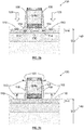
- the figure 3 summarizes the main steps 410 to 440 of a detailed example of a method for forming the spacers of a transistor according to the invention. These steps 410 to 440 can also be applied to the formation of spacers on the sides of the gates of various transistors: FDSOI, FinFET, etc. Steps 410 to 440 will be detailed in the paragraphs below regarding Figures 4a to 4d and 5a to 5e respectively illustrating a structure of a transistor 200 obtained at the end of one of the steps 410 to 440 according to one embodiment of the invention.
- the figure 4a illustrates a structure obtained at the end of the forming step 410 of a protective layer 152 covering a transistor 200 formed on a SOI substrate 140 comprise an active layer 146 surmounted by a gate 120 of the transistor 200.
- the formation of the transistor 200 consists in producing an elaborate substrate 140 of the SOI type, from a substrate 142, often referred to as bulk substrate (bulk substrate), an initial insulating layer 144 and the active layer 146, the latter being intended to subsequently form a conduction channel of the transistor 200.
- the semiconductor material is taken from: germanium (Ge), silicon germanium (SiGe).
- a thin insulating layer of gate oxide 121 through which an electric field is able to pass. develop to create an underlying conduction channel between source and drain when a sufficient electrical voltage is applied to the gate 120.
- the dielectric layer 121 is made of an insulating material with high permittivity ( high-k) covered by a metal layer (metal gate, not shown in figures) of the grid 120.
- the stack of layers of the grid 120 also comprises a hard mask 126 of protection which will be removed later to allow the resumption of contact on this electrode.
- This hard mask 126 which remains in place after etching the gate, is typically made of silicon oxide (SiO2). Its role is to protect the top of the grid 120 from any damage during the completion of the following steps and in particular those of etching spacers.
- the dielectric layer 121 is disposed in contact with the active layer 146 forming the conduction channel.
- the metal layer is disposed in contact with the dielectric layer 121.
- the polycrystalline silicon layer 123 is disposed directly in contact with the gate oxide formed by the dielectric layer 121 if the metal layer is absent or is disposed directly in contact with the metal layer.
- a structure 300 distinct from the transistor 200 is formed, prior to the forming step 410 of the protective layer 152, on the substrate 140 on which the grid 120 rests.
- this structure 300 is optional.
- the transistor 200 is an NMOS transistor and the structure 300 is a PMOS transistor.
- the transistor 200 is a PMOS transistor and the structure 300 is an NMOS transistor.
- the forming step 410 of the protective layer 152 is performed so as to cover the transistor 200 and the structure 300, that is to say on all the surfaces, vertical and horizontal, devices being manufactured. This is a deposit that can be described as compliant.
- the protective layer 152 is disposed directly in contact with the surfaces of the structures being manufactured.
- This forming step 410 is preferably, but not exclusively, using a deposit method known as LPCVD, the acronym for “low pressure chemical vapor deposition”, that is to say “chemical deposition in low pressure vapor phase ".
- LPCVD low pressure chemical vapor deposition
- This type of deposit which is practiced at atmospheric pressure allows indeed a uniform deposit on all surfaces regardless of their orientation.
- This protective layer 152 may be based on nitride (N) and / or silicon (Si) and / or carbon (C). It has a dielectric constant equal to or less than 7.
- the protective layer 152 is for example a silicon nitride (SiN) layer whose dielectric constant is equal to 8 and preferably to 7.
- the protective layer 152 comprises a material having a low dielectric constant less than 4 and preferably less than 3.1 and preferably less than or equal to 2.
- materials such as SiCO, SiC SiCN, SiOCN, SiCBN, SiOCH, c-BN, boron nitride (BN) and SiO2 are referred to as "low-k" materials, i.e. dielectric.
- the material of the protective layer 152 taken from the "low-k" materials as above thus makes it possible to reduce the parasitic capacitance in order to improve the performance of the transistor.
- the invention is nevertheless not limited to the examples of materials as above.
- the protective layer 152 may be of another material having a low dielectric constant less than or equal to 8 and preferably 7.
- the protective layer 152 is a porous layer.
- the protective layer 152 is a non-porous layer.
- the material of the protective layer 152 is compatible with dry or wet cleaning performed at a next step 440 to remove a modified protective layer 158 (described later).
- the thickness of the protective layer 152 is preferably sufficiently large so that after the completion of the modification 430 and the removal step 440, there remain unmodified portions 152a, 152b of the protective layer 152 at the flanks from the grid 120.
- the thickness of the protective layer 152 is between 5 nm and 30 nm, preferably 10 nm.
- the method of the invention comprises an optional step of reducing the dielectric constant of the protective layer 152.
- the reduction of the dielectric constant is obtained during the step depositing the protective layer 152.
- the reduction of the dielectric constant comprises the introduction into the protective layer 152 in forming precursors which form bonds reducing the polarizability of the layer 152.
- precursors are chosen so as to generate less polar bonds as silicon nitride, such as Si-F, SiOF, Si-O, CC, CH, and Si-CH3.
- the reduction of the dielectric constant comprises the introduction into the protective layer 152 forming a porosity.
- the figure 4b illustrates the structure of the transistor 200 at the end of an optional deposition step 310 of a layer 311 comprising carbon, this layer 311 comprising carbon being distinct from said transistor 200.
- the layer 311 comprising carbon is configured to cover the structure 300 distinct from said transistor 200, the structure 300 and said transistor 200 being on the same substrate 140.
- This layer 311 comprising carbon can serve as protection for the structure it covers.
- the layer 311 comprising carbon is a photosensitive or thermosensitive resin layer.
- the layer 311 comprising carbon is a hard mask comprising carbon and preferably formed of carbon.
- the figure 4c illustrates the structure of the transistor 200 at the end of the modification step 430 of the protective layer 152 and the formation of a carbon film 271.
- the modification step 430 of the protective layer 152 as formed at the end of step 410 is done by bringing the protective layer 152 into contact with a plasma comprising ions heavier than hydrogen. and CxHy where x is the proportion of carbon and y is the proportion of hydrogen and ions heavier than hydrogen, to form a modified protective layer 158 and a carbonaceous film 271.
- CxHy is introduced into the plasma, for example methane (CH4) to perform the functions "a” and "c".
- CH4 methane
- the chemical species of the plasma containing carbon from CH4 or more generally from CxHy provide the "a" function.
- the plasma comprises heavier ions than hydrogen such as helium (He), argon (Ar), nitrogen (N2), xenon (Xe) and oxygen (O2).
- these ions are referred to in the following description "heavy ions”.
- the "c” function is provided by hydrogen-based ions.
- the hydrogen-based ions are preferably taken from: H, H + , H 2 + , H 3 + .
- hydrogen ions These ions have the property of penetrating easily and deeply into the protective layer 152. They thus modify the protective layer 152 but without spraying it.
- the heavy ions penetrate much less deeply into the protective layer 152. These heavy ions remain localized on the surface and are therefore not able to modify a significant thickness, and a fortiori the entire thickness, of the protective layer 152.
- the depth Heavy ion penetration is about ten times lower than the penetration depth of hydrogen ions.
- the hydrogen-based ions can be implanted in the material to be etched, without causing dislocation of its atomic structure such that it would cause a sputtering of the latter, and therefore without redeposition of the etched material on the walls of the reactor or the patterns being etched themselves, are likely to be suitable.
- This additional function consists of dissociating the molecule CxHy in order to release the species H.
- Helium (He) is particularly effective for this function.
- the mixture introduced into the plasma reactor thus preferably comprises a CxHy / He mixture.
- this modification step 430 of the layer to be etched can be practiced in many different ways by adapting all kinds of means commonly used by the microelectronics industry.
- Standard etchings are used in which low or high density plasmas can be developed and where the energy of the ions can be controlled to allow the implantation of the light species above to modify the layer to be etched.
- immersion plasma commonly used for practicing implantation of species on the surface of a device during manufacture.
- a modification of the layer performed by an implantation using a plasma has the advantage of allowing a continuous implantation from the free surface of the protective layer 152 and a small thickness, typically between 0 and 100 nm or even between 0 and 30 nm. It also makes it possible to benefit from improved selectivity from the beginning of etching and from a constant etching rate, leading to improved etching accuracy.
- the use of a plasma to implant the protective layer 152 thus makes it possible to remove a very thin layer, typically between 1 and 10 nm and more generally between 1 and 30 nm.
- This step of modification 430 is performed so that the plasma is anisotropic so as to bombard the ions in a preferred direction 351 parallel to the sidewalls of the gate 120.
- the plasma used in this step 430 creates a bombardment of ion-based ions.
- hydrogen (H) from the CxHy molecule and implanting itself in an upper portion of the thickness of the protective layer 152 at the sides of the gate 120.
- These ions based on of hydrogen come from the CxHy whose molecule is dissociated by ions heavier than hydrogen from the plasma.
- the ions modify the surfaces perpendicular to the direction of the bombardment to a greater thickness than the surfaces parallel to the direction of the bombardment.
- the upper portion of the thickness of the protective layer 152 at the edges of the gate 120 is modified to a lesser thickness than the surface at the top of the gate 120 and the surfaces of the protective layer 152 covering the active layer. 146.
- An unmodified thickness 152a, 152b of the protective layer 152 covering the sidewalls of the grid 120 is retained and will become spacers 152a, 152b.
- the hydrogen-based ions enter the protective layer 152 to modify it.
- CxHy preferably CH4
- plasma tends to deposit a carbon film 271 on the different walls.
- the bombardment of ions heavier than hydrogen allows the carbon species from the CxHy to form the carbonaceous film 271, especially on surfaces parallel to the direction of the bombardment, while preventing the formation of a carbon film 271 on the surfaces of the film.
- protective layer 152 which are perpendicular to the direction 351 of the bombardment, such as the bottom of the trenches.
- the heavy ions of the plasma pulverize the carbon species coming from the CxHy which would have a tendency to form on these walls perpendicular to the direction of implantation and thus prevent the growth of this carbon film 271 on these walls perpendicular to the direction of implantation.
- this carbon film 271 is formed on surfaces that receive less bombardment or do not receive bombardment. Thus, it is formed in particular on the surfaces parallel to the direction 351 of the bombardment.
- the carbon film 271 acts as a carbon protection layer for the protective layer 152 that it covers, reducing the thickness on which the hydrogen ions penetrate into the protective layer 152 and modifies the latter .
- the carbon film 271 makes it possible to increase the difference in thickness of modification between the surfaces covered by the carbon film 271 and the surfaces that are not. This controls the engraved thickness even better.
- the concentration of ions heavier than hydrogen in the plasma is between 50% and 98% and preferably between 55% and 85% and 60% and 80%. These concentrations are usually measured by a ratio between the two gaseous components.
- a ratio between two gaseous components is a ratio relating to the respective rates of introduction of the components into the plasma reactor.
- Each flow is usually measured in sccm.
- a flow rate is measured with a flow meter associated with the reactor.
- the protective layer 152 is modified by the H ions coming from the CH4 gas. He ions destroy or prevent the formation of the carbonaceous film 271 which would tend to form on the surfaces perpendicular to the direction 351 such as the surfaces of the modified protective layer 158 covering the active layer 146 and the hard mask 126 at the top of the grid 120 .
- the nature of the Argon ions and the parameters of the plasma, in particular its energy, make it possible to ensure a depletion of the methyl groups of the carbonaceous film. 271 made anisotropically, so that the carbonaceous film 271 is not formed on the surfaces perpendicular to the direction 351 as above.
- argon can prevent, possibly alone, also the formation of the carbon film on the surfaces perpendicular to the direction 351 of bombardment. Combined with He, N2, Xe and / or O2, it helps to pulverize the carbon film 271 which would tend to form.
- the heavy ions Ar, He, N2, Xe or O2 make it possible to reinforce the action of the hydrogen-based ions by also preventing the formation of the carbon film 271 on the surfaces perpendicular to the main direction 351 of the bombardment.
- the H ions of the CH4 participate in synergy with the heavy ions of the plasma (He, Ar, N2, Xe or O2 for example) in the modification of the portion 158 of the protective layer. , although the penetration depth of these heavy ions is lower than that of hydrogen-based ions.
- the carbon film 271 formed covers only the surfaces of the protective layer 152 which are perpendicular or strongly inclined with respect to the plane of the substrate 140, such as the upper surfaces of the layer modified guard 158 at the edges of the gate 120 and the walls or flanks of the layer 311 comprising carbon.
- the carbon film 271 is formed on the walls of the layer 311 comprising carbon.
- the plasma ions do not spray the carbon film 271 formed on the walls of the layer 311 comprising carbon. This is likely due to the chemical affinities and molecular reactions between the carbon of the 311 layer and the carbon-containing chemical species from the CxHy. This affinity accelerates the obtaining of a deposition regime and promotes the formation of the carbonaceous film 271 on the layer 311 comprising carbon.
- the carbon film 271 is therefore formed quickly and despite the bombardment of heavy ions.
- This carbon film 271 thus acts as a protective layer for the layer 311 comprising carbon and prevents the latter from being degraded by ion bombardment. The dimensions of the layer 311 are thus preserved despite the ion bombardment.
- the thickness e2 of the carbonaceous film 271 covering the walls of the layer 311 comprising carbon is greater than the thickness e1 of the carbonaceous film 271 on the protective layer 152 (at the flanks of the the grid 120). Even more advantageously, the thickness e2 of the carbon film 271 is at least two times greater than the thickness e1 of the carbon film 271. The thicknesses e1 and e2 appear on the figure 4c .
- the thickness e1 of the carbon film 271, measured on a sidewall of the grid 120 and perpendicular to the sidewall, is preferably very thin, for example between 1 and 5 nm, preferably 1 nm.
- the thickness e2 of the carbon film 271, measured on the layer 311 comprising carbon and parallel to the implantation direction, is for example 5 nm or between 1 and 10 nm.
- the carbon film 271 formed on the layer 311 comprising carbon is thus thicker than that on the protective layer 152 because of the chemical reactions between the carbon of the layer 311 and the carbon provided by the CxHy of the plasma.
- the thickness e2 of the carbonaceous film 271 formed on the layer 311 comprising carbon enables it to withstand ion bombardment carried out anisotropically as above.
- this reinforced or thickened carbon film 271 makes it possible to protect the layer 311 comprising carbon during the modification step 430 as well as during the withdrawal step 440 and this even on the surfaces perpendicular to the direction 351 of the bombardment.
- the carbonaceous film 271 acts as a protective layer for the layer 311 comprising carbon, preventing or reducing the modification of the latter under the effect of ion bombardment.
- modification step 430 can be practiced in many different ways by adapting all kinds of means commonly used by the microelectronics industry, such as using any type of burner, for example in a reactor.
- CCP type reactor of the English “Capacitive Coupled Plasma” that is to say “plasma to capacitive coupling "which controls the energy of the ions.
- immersion plasma commonly used for practicing implantation of species on the surface of a device during manufacture.
- the person skilled in the art in order to determine the behavior of the material to be etched in the chosen type of implanter, will preferentially proceed to "full-plate” tests in order to establish behavior curves. He will deduce the parameters of the implantation, in particular the energy and the dose of ions, that is to say the exposure time, to use to reach the desired thickness of material to be modified.
- the following table gives typical conditions for implementing the modification step 430 of the protective layer 152, carried out using a plasma of He / CH4, H2 / CH4 / Ar, CH4 / Ar, CH4 / N2, or CH4 / N2 / H2, as a function of time in seconds and the power polarization (bias) in watts, etc. These conditions are largely dependent on the thickness to be modified of the protective layer 152.
- the protective layer 152 is a nitride-based layer such as a silicon nitride layer.
- Engraving reactor ICP or CCP reactor or by plasma immersion of He / CH4 (He: 50-500 sccm, CH4: 5-15 sccm), or H2 / CH4 / Ar or H2 / CH4 / N2 plasma (H2: 50-500 sccm) , CH4: 5-15 sccm, Ar (Argon) or N2: 100-1000 sccm)
- Thickness of the protective layer 152 to be modified Thickness of the modified protective layer 158): 1 - some ten nm, for example 6-10nm
- Power of the source 0 - 2000 Watts Polarization power (ion energy): 20 - 500 V Pressure: 5 milli Torr - 10 milli Torr Temperature : 10 - 100 ° C Time : a few seconds to a few hundred seconds
- the protective layer 152 is modified over its entire thickness above the gate 120 and above the active layer 146 and while leaving in place unmodified portions 152a, 152b of the protective layer 152 at the level of the sides of the grid 120.
- the figure 4d illustrates the result of the removal step 440 of the modified protective layer 158 after a selective etching operation of the modified protective layer 158 with respect to: the carbonaceous film 271, at the unmodified portions 152a, 152b of the protective layer 152 and the active layer 146.
- the etching solution thus etches the modified protective layer 158 to which it has direct access on the top of the grid 120 and in the bottom of the trenches.
- a thickness of the protective layer located on the sides of the grid is then modified.
- the etching solution can also be introduced into the space located at the edges of the gate 120, between the carbon film 271 covering the sidewalls and the unmodified portions 152a, 152b.
- the etching solution consumes the modified protective layer 158.
- the passages taken by the etching solution to consume this portion of the protective layer modified protection 158 are referenced 272 on the figure 4c .
- the carbon film 271 is no longer supported and disappears. Typically this disintegration of the carbon film is called “lift off” or withdrawal by lifting.
- the protective layer located on the sides of the grid is not changed or very little changed.
- the etching solution does not remove the protective layer 152 located on the sidewalls.
- the carbon film 271 thus remains maintained by the latter. It does not disappear then during the withdrawal step.
- the carbon film 271 of thickness e2 protects the layer 311 comprising carbon during this removal step 440.
- the etching solution does not consume advantageously or only a little of the layer 311 comprising carbon.
- the realization of the withdrawal step 440 therefore does not lead to a consumption of the layer 311 comprising carbon.
- the parameters of the removal step are also adjusted so that the modified protective layer 158 can be etched selectively with respect to a layer made of an oxide, typically an oxide of said semiconductor material, the latter forming for example a gate oxide layer.
- the selective etching of the modified protective layer 158 does not consume silicon oxide SiO2.
- these parameters are also adjusted so that the modified protective layer 158 can be etched selectively with respect to the semiconductor material of the active layer 146.
- the removal step 440 is carried out by wet etching using a hydrofluoric acid (HF) etching solution.
- HF hydrofluoric acid
- the shrinkage step 440 may be performed by wet etching using a hydrofluoric acid (HF) etching solution or of phosphoric acid (H3PO4) for SiC, SiCN or SiN.
- HF hydrofluoric acid
- H3PO4 phosphoric acid
- the etching of the protective layer 158 is changed selectively as possible with respect to silicon especially in order not to attack the silicon of the active layer 146.
- wet etching it there is no silicon consumption of the active layer 146 due to the use of the hydrofluoric acid (HF) etching solution.
- HF hydrofluoric acid
- the thickness of the modified protective layer 158 is typically in a range of values from 1 nm to a few tens of nm. Burning times can range from a few seconds to a few minutes, obviously being directly dependent on the thickness that has been modified.
- etching time is obtained with 85% diluted phosphoric acid (H3PO4) to etch a layer of silicon nitride (SiN) or SiC.
- a solution of hydrofluoric acid (HF) can be used for protective layers based on other materials than nitride, silicon and carbon.
- the stopping of said selective etching can therefore be done on the unmodified portions 152a, 152b of the protective layer 152 and / or on the monocrystalline silicon of the active layer 146 or / and again on the hard mask 126 at the top of the gate 120, until the disappearance of the modified protective layer 158.
- wet etching is preferably used which combines the removal of the modified protective layer 158 with wet cleaning of the wafer containing the devices being manufactured, because after this etching wet, conventionally wet cleaning (translation of English "wet clean") is performed to clean a wafer on which is the transistor 200.
- this wet etching is combined with wet cleaning, which simplifies the process and saves time.
- the wet cleaning parameters are also adjusted so that the modified protective layer 158 can be etched very selectively with respect to the carbon-containing species of the carbonaceous film 271, in particular covering the walls of the layer 311 comprising the carbon, and to the portions unmodified (the spacers obtained) 152a, 152b of the protective layer 152.
- a dry etch of the modified silicon protection layer 158 of the active layer 146, the material of the spacers 152a, 152b, and the silicon oxide (SiO2) of the hard mask 126 can then be performed for this step of dry removal of the modified protective layer 158.
- the principle of the dry shrinkage of the modified protective layer 158 typically a nitride-based modified layer 158 comprises the following steps 610 to 630 illustrated in FIG. figure 6 which take place in a reaction chamber where a plasma is formed.
- the thicknesses treated are typically between 1 nm and a few tens of nanometers.
- the principle of dry removal of the modified protective layer 158 is close to that described in the above publication. The difference is that in the case of the invention no silicon oxide is etched but the modified protective layer 158 by using a plasma such as H2 / CH4 / Ar.
- a first step 610 consists in generating the etching product in the plasma according to the following chemical reaction: NF 3 + NH 3 ⁇ NH 4 F + NH 4 F.HF which reacts nitrogen trifluoride (NF 3 ) with ammonia (NH 3 ).
- Etching is carried out during a second step 620, at a temperature of the order of 30 ° C. and more generally between 10 ° C. and 50 ° C., in the form of a salt formation according to the following chemical reaction : NH 4 F or NH 4 F.HF + SiNH ⁇ (NH 4 ) 2SiF 6 (solid) + H 2
- the streams of nitrogen trifluoride (NF 3 ) and ammonia (NH 3 ) are respectively 50 sccm and 300 sccm at 30 ° C. for 45 seconds for step 620 of forming salts which is followed by the sublimation step 630 which is carried out at 180 ° C for 60 seconds.
- This embodiment makes it possible to obtain a very good selectivity of the etching of the modified protective layer 158 with respect to the unmodified portions 152a, 152b and to the unmodified semiconductor material.
- this selectivity of the etching is much greater (typically a factor of at least 10) than that obtained with a solution of HF.
- Unmodified 152a, 152b of the initial protective layer 152 remain essentially on the sidewalls of the stack of layers that form the grid 120.
- Unmodified 152a, 152b constitute the spacers 152a, 152b for the gate 120 of the transistor 200, for example of the FDSOI type.
- the etching of the modified protective layer 158 can also be performed for the production of the spacers of a three-dimensional transistor FinFET type without this application being limiting of the invention.
- the result of the figure 4d may be the result of a single modification step and a single withdrawal step or a plurality of sequences comprising these steps.
- the modification operations 430 of the protective layer 152 and the removal layer 440 of the modified protective layer 158 may optionally be repeated 450.
- the sequences each comprising a modification step 430 and a withdrawal step 440 are carried out until complete removal of the protective layer 158 outside the sides of the gate 120.
- the number of sequences is calculated according to the etching rate of the first sequence.
- Additional steps may for example be standard steps where the extensions of the source / drain zones may be carried out by ion implantation of dopants before epitaxial growth of the raised source / drain of FDSOI transistors.
- the embodiment illustrated in Figures 4a to 4d shows the manufacture of the spacers 152a, 152b of the transistor 200, for example of the PMOS type, without consuming the layer 311 comprising carbon covering the structure 300 such as an NMOS type transistor, in order to prevent the layer 311 comprising carbon from be damaged by performing the modification 430 and withdrawal 440 steps.
- the method of the invention can be applied to fabricate microelectronic devices on the same substrate on which none of the devices being manufactured are covered and protected by a protective layer such as the layer 311 comprising carbon.
- FIG. Figures 5a, 5b and 5th An embodiment without depositing a layer 311 comprising carbon is illustrated in FIG. Figures 5a, 5b and 5th .
- the figure 5a illustrates a structure obtained at the end of the forming step 410 of a protective layer 152 covering a transistor 500 formed on a SOI type substrate 140 comprise an active layer 146 surmounted by a gate 120 of the transistor 500.
- the starting structure of transistor 500 is similar to that of transistor 200 as illustrated in FIG. figure 4a .
- This training step 410 is not different from that illustrated above with reference to the embodiment described in FIG. Figures 4a to 4d .
- no deposition step of a layer comprising carbon (such as the layer 311 as described above) is performed so as to cover another structure previously formed on the substrate 140.
- the figure 5b shows the structure of the transistor 500 obtained at the end of the modification step 430 according to the present embodiment.
- the modification step 430 is a single step performed so as to modify the protective layer 152 throughout its thickness on all the surfaces parallel to the plane of the substrate 140 on which the gate 120 of the transistor 500 rests and not to modify the protective layer 152 throughout its thickness on the surfaces perpendicular to this plane.
- step 430 The type of plasma used and the implementation conditions for implementing this modification step 430 are similar to those of step 430 of the embodiment illustrated previously in FIG. Figures 4a to 4d .
- the carbon film 271 formed covers only the surfaces perpendicular to the plane of the substrate 140, such as the upper surfaces of the modified protective layer 158 at the edges of the grid 120.
- the carbon film 271 is preferably very fine, for example between 1 and 5 nm, preferably 1 nm.
- the carbon film 271 of the present embodiment is not formed on the surfaces perpendicular to the direction 351 due to ion bombardment of He or Ar made anisotropically.
- the figure 5e shows the final structure of the removal step 440 of the modified protection layer 158 according to the present embodiment.
- This retraction step 440 is performed to etch the modified protective layer 158 by selectively etching the unmodified portions 152a, 152b of the protective layer 152, and / or the semiconductor material of the active layer 146 and / or the silicon oxide (SiO2) of the hard mask 126 at the top of the gate 120.
- This removal step can be combined with a standard cleaning step to simplify the process, which saves time.
- the etching is also selective with respect to the chemical species containing carbon, typically carbon, of the carbon film 271. Nevertheless, when the modified protective layer 158 disappears at the edges of the grid 120, the film carbon 271 very thin (for example 1 nm) disintegrates because it is no longer supported.
- step 440 The type of selective etching and the implementation conditions for implementing this retraction step 440 are similar to those of step 440 of the embodiment illustrated previously in FIG. Figures 4a to 4d .
- FIG. figures 5a , 5c at 5th Another embodiment without depositing a layer 311 comprising carbon is illustrated in FIG. figures 5a , 5c at 5th.
- the present embodiment begins with the step 410 of forming a protective layer 152 covering a transistor 500, as previously illustrated in FIG. figure 5a .
- the figure 5c shows the structure of the transistor 500 obtained at the end of an optional anisotropic etching step 320 of the protective layer 152.
- an anisotropic etching 320 of the protective layer 152 is thus, according to this optional and nonlimiting embodiment, carried out in two stages comprising: a first step called “main etching” performed isotropically, and a second finishing step generally referred to as "overgrading” or of the English term “over etching (OE)” having the same meaning. It is during the overgrafting step (steps 440) that the protective layer 152 remaining on the horizontal surfaces will be removed, after modifying (step 430) the protective layer 152 to avoid or limit the problems described in Figures 2a to 2c .
- the next step to be carried out is the modification step 430 of the protective layer 152 remaining at the end of the anisotropic etching step 320.
- the structure of the transistor 500 at the end of this step 430 is illustrated in FIG. figure 5d .
- This modification step 430 is not different from that of the embodiment illustrated previously in Figures 5a, 5b and 5th nor that of the embodiment illustrated above in Figures 4a to 4d .
- the removal step 440 of the modified protective layer 158 is then performed, as illustrated in FIG. figure 5e .
- This removal step 440 is not different from that of the embodiment illustrated previously in FIG. Figures 5a, 5b and 5th nor that of the embodiment illustrated above in Figures 4a to 4d .
- This embodiment makes it possible to rapidly remove a large protective layer thickness modified by isotropic etching and then to precisely control the thickness of the spacers by performing steps 430 and 440.
- this step will therefore be avoided, which will be replaced by a repetition 450 of the modification operations 430 of the protective layer 152 and of the withdrawal layer 440 of the modified protective layer 158, the removal being preferably done in this case. case in the form of a dry withdrawal as described in figure 6 since, as noted above, the two operations can be performed in the same etching reactor.
- a carbonaceous film formed during the process modification step resists plasma ion bombardment, thereby protecting the carbon-containing layer during the modification step as well as during the removal step.
- the method of the invention is particularly advantageous for forming the spacers of MOSFET or FinFET type transistors.
- the method of the present invention makes it possible to very precisely control the dimension of the spacers while overcoming or reducing the problems detailed previously, for example: the excessive consumption of the active layer and / or of a carbon mask or of a photosensitive resin layer typically comprising carbon, the formation of feet at the spacers of the grid at the interface with the SOI substrate as described in FIG. Figures 2a and 2b as well as the erosion of the spacers of the grid as described in Figure 2c .
Landscapes
- Engineering & Computer Science (AREA)
- Power Engineering (AREA)
- Microelectronics & Electronic Packaging (AREA)
- General Physics & Mathematics (AREA)
- Computer Hardware Design (AREA)
- Physics & Mathematics (AREA)
- Condensed Matter Physics & Semiconductors (AREA)
- Manufacturing & Machinery (AREA)
- Chemical & Material Sciences (AREA)
- Ceramic Engineering (AREA)
- Inorganic Chemistry (AREA)
- Chemical Kinetics & Catalysis (AREA)
- General Chemical & Material Sciences (AREA)
- Crystallography & Structural Chemistry (AREA)
- Metal-Oxide And Bipolar Metal-Oxide Semiconductor Integrated Circuits (AREA)
Claims (15)
- Verfahren zum Bilden von Abstandshaltern (152a, 152b) eines Gates (120) eines Feldeffekttransistors (200), wobei das Gate (120) einen Scheitel und Flanken aufweist und sich oberhalb einer Wirkschicht (146) aus einem Halbleitermaterial befindet, dadurch gekennzeichnet, dass es umfasst:- zumindest einen Schritt des Ausbildens (410) einer das Gate (120) überdeckenden Schutzschicht (152), wobei die Schutzschicht (152) eine Schicht auf Basis von Nitrid (N) und/oder auf Basis von Silicium (Si) und/oder auf Basis von Kohlenstoff (C) ist, die eine Dielektrizitätskonstante gleich oder unter 8 aufweist;- zumindest einen Schritt des Modifizierens (430) der Schutzschicht (152) durch Inkontaktbringen der Schutzschicht (152) mit einem Plasma, in das CxHy eingebracht wird, wobei x der Anteil an Kohlenstoff (C) ist und y der Anteil an Wasserstoff (H) ist, und Ionen schwerer als Wasserstoff enthält; wobei die Plasmabedingungen, insbesondere die CxHy-Konzentration, die Energie der Plasmaionen und die Implantationshauptrichtung so gewählt sind, dass:∘ das Plasma eine Bombardierung mit Ionen auf Basis von Wasserstoff (H, H+, H2 +, H3+, etc.) aus dem CxHy schafft, wobei die Bombardierung anisotrop in der Implantationshauptrichtung ist, die parallel zu den Flanken des Gates (120) verläuft, so dass eine modifizierte Schutzschicht (158) gebildet wird, indem die Abschnitte (158) der Schutzschicht (152), die am Scheitel des Gates (120) und beiderseits des Gates (120) liegen, modifiziert werden, und so dass nicht modifizierten Abschnitte (152a, 152b) der Schutzschicht (152) erhalten bleiben, die die Flanken des Gates (120) überdecken,∘ chemische Spezies des Plasmas, die Kohlenstoff enthalten, das aus CxHy stammt, einen kohlenstoffhaltigen Film (271) insbesondere an den Oberflächen bilden, die parallel zur Implantationshauptrichtung (351) verlaufen;∘ das Plasma eine Bombardierung mit Ionen schwerer als Wasserstoff schafft, welche die chemischen Spezies des Plasmas, die Kohlenstoff enthalten und aus CxHy stammen, daran hindert, einen kohlenstoffhaltigen Film (271) insbesondere an den Oberflächen der Schutzschicht (152) zu bilden, die senkrecht zur Implantationshauptrichtung (351) verlaufen;- zumindest einen Schritt des Entfernens (440) der modifizierten Schutzschicht (158) mit Hilfe einer selektiven Ätzung der modifizierten Schutzschicht (158) gegenüber der nicht modifizierten Abschnitte (152a, 152b) der Schutzschicht (152).
- Verfahren nach Anspruch 1, wobei die Schutzschicht (152) eine Dielektrizitätskonstante unter 4 und vorzugsweise unter 3.1 und bevorzugt unter oder gleich 2 aufweist.
- Verfahren nach einem der vorangehenden Ansprüche, wobei die Schutzschicht (152) eine Schicht auf Basis von Nitrid (N) und vorzugsweise eine Siliciumnitridschicht (SiN) ist.
- Verfahren nach einem der Ansprüche 1 oder 2, wobei die Schutzschicht (152) eine Schicht auf Basis von Silicium (Si) oder auf Basis von Kohlenstoff (C) ist und wobei das Material der Schutzschicht (152) ausgewählt ist aus: SiCO, SiC, SiCN, SiOCN, SiCBN, SiOCH, CBN, Bn, SiCBO und SiO2.
- Verfahren nach einem der vorangehenden Ansprüche, wobei die Schutzschicht (152) eine poröse Schicht ist.
- Verfahren nach einem der vorangehenden Ansprüche, wobei der Schritt des Ausbildens (410) der Schutzschicht (152) einen Schritt des Aufbringens der Schutzschicht (152) umfasst, bei dem ein Schritt der Verringerung der Dielektrizitätskonstante der Schutzschicht (152) erfolgt und wobei vorzugsweise der Schritt des Verringerns der Dielektrizitätskonstante der Schutzschicht (152) das Einbringen einer Porosität in die Schutzschicht (152) umfasst und/oder wobei der Schritt des Ausbildens (410) der Schutzschicht (152) das Einbringen von Vorläufern in die Schutzschicht (152) während des Aufbringens umfasst.
- Verfahren nach Anspruch 1, wobei der Schritt des Ausbildens (410) der Schutzschicht (152) einen Schritt des Aufbringens der Schutzschicht (152) umfasst, während dessen ein Schritt des Verringerns der Dielektrizitätskonstante der Schutzschicht (152) erfolgt, wobei der Schritt des Ausbildens (410) der Schutzschicht (152) das Einbringen von Vorläufern in die Schutzschicht (152) während des Aufbringens umfasst, wobei die Schutzschicht eine Schicht auf Basis von Siliciumnitrid ist und wobei die Vorläufer so ausgewählt sind, dass weniger polare Bindungen als Siliciumnitrid, wie etwa Si-F, SiOF, Si-O, C-C, C-H und Si-CH3, bilden.
- Verfahren nach einem der vorangehenden Ansprüche, wobei bei dem Schritt des Modifizierens (430) der Schutzschicht (152) die CxHy-Konzentration in dem Plasma zwischen 2 % und 50 % und vorzugsweise zwischen 8 % und 40 % beträgt und wobei vorzugsweise bei dem Schritt des Modifizierens (430) der Schutzschicht (152) die Konzentration an schweren Ionen als Wasserstoff in dem Plasma zwischen 50 % und 98 % beträgt.
- Verfahren nach einem der vorangehenden Ansprüche, das vor dem Schritt des Modifizierens (430) einen Schritt des Aufbringens (310) einer kohlenstoffhaltigen Schicht (311) umfasst, wobei diese kohlenstoffhaltige Schicht (311) gesondert vom Transistor (200) vorliegt, und wobei das Ätzen der modifizierten Schutzschicht (158) selektiv gegenüber dem Kohlenstoff (271) und gegenüber den nicht modifizierten Abschnitten (152a, 152b) der Schutzschicht (152) erfolgt.
- Verfahren nach dem vorangehenden Anspruch, wobei die kohlenstoffhaltige Schicht (311) dazu ausgelegt ist, eine von dem Transistor (200) gesondert vorliegende Struktur (300) zu überdecken und wobei der Transistor (200) ein NMOS-Transistor ist und die Struktur (300) ein PMOS-Transistor ist, oder wobei der Transistor (200) ein PMOS-Transistor ist und die Struktur (300) ein NMOS-Transistor ist.
- Verfahren nach einem der vorangehenden Ansprüche, wobei der Schritt des Modifizierens (430) so erfolgt, dass das Plasma eine Bombardierung mit schwereren Ionen als Wasserstoff in anisotroper Weise in der parallel zu den Flanken des Gates (120) verlaufenden Implantationshauptrichtung erzeugt, so dass die chemischen Spezies des Plasmas, die Kohlenstoff enthalten und aus CxHy stammen, daran gehindert werden, einen kohlenstoffhaltigen Film (271) an den Oberflächen zu bilden, die senkrecht zu den Flanken des Gates (120) verlaufen.
- Verfahren nach einem der vorangehenden Ansprüche, wobei der Schritt des Modifizierens (430) so erfolgt, dass die schwereren Plasmaionen als Wasserstoff das Molekül von CxHy dissoziieren, so dass den aus CxHy stammenden Wasserstoff-Ionen (H) ermöglicht wird, Ionen auf Basis von Wasserstoff zu bilden und sich in den Abschnitten (158) der Schutzschicht (152) zu implantieren.
- Verfahren nach einem der vorangehenden Ansprüche, wobei beim dem Schritt des Modifizierens (430) die Plasmabedingungen, insbesondere die CxHy-Konzentration, die Energie der Ionen und die Implantationshauptrichtung, so gewählt sind, dass im Bereich der Oberflächen, die senkrecht zur Implantationshauptrichtung verlaufen, die gesamte Dicke der Schutzschicht (152) durch die Implantation von Ionen auf Basis von Wasserstoff modifiziert wird und wobei der Schritt des Entfernens (440) so erfolgt, dass die gesamte modifizierte Schutzschicht (158) entfernt wird, wobei dadurch die Wirkschicht (146) im Bereich der senkrecht zur Implantationshauptrichtung verlaufenden Flächen freigelegt wird.
- Verfahren nach einem der vorangehenden Ansprüche, wobei der Schritt des Entfernens (440) der modifizierten Schutzschicht (158) durch Nassätzen erfolgt.
- Verfahren nach einem der Ansprüche 1 bis 13, wobei der Schritt des Entfernens (440) durch selektives Trockenätzen der modifizierten Schutzschicht (158) gegenüber dem kohlenstoffhaltigen Film (271), gegenüber den nicht modifizierten Abschnitten (152a, 152b) der Schutzschicht (152) und gegenüber dem Halbleitermaterial erfolgt, wobei vorzugsweise das Trockenätzen in einem Plasma erfolgt, das in einem Sicherheitsbehälter ausgehend von Stickstofftrifluorid (NF3) und Ammoniak (NH3) gebildet wird, und wobei vorzugsweise das Trockenätzen umfasst:- einen Schritt des Ätzens (620), der in der Bildung von festen Salzen besteht;- einen Schritt der Sublimation (630) der festen Spezies.
Applications Claiming Priority (1)
| Application Number | Priority Date | Filing Date | Title |
|---|---|---|---|
| FR1555666A FR3023973B1 (fr) | 2014-07-18 | 2015-06-19 | Procede de formation des espaceurs d'une grille d'un transistor |
Publications (2)
| Publication Number | Publication Date |
|---|---|
| EP3107124A1 EP3107124A1 (de) | 2016-12-21 |
| EP3107124B1 true EP3107124B1 (de) | 2018-04-04 |
Family
ID=55070972
Family Applications (1)
| Application Number | Title | Priority Date | Filing Date |
|---|---|---|---|
| EP16151402.1A Active EP3107124B1 (de) | 2015-06-19 | 2016-01-15 | Verfahren zur bildung von abstandshaltern eines gates eines transistors |
Country Status (1)
| Country | Link |
|---|---|
| EP (1) | EP3107124B1 (de) |
Family Cites Families (8)
| Publication number | Priority date | Publication date | Assignee | Title |
|---|---|---|---|---|
| DE3420347A1 (de) | 1983-06-01 | 1984-12-06 | Hitachi, Ltd., Tokio/Tokyo | Gas und verfahren zum selektiven aetzen von siliciumnitrid |
| US5786276A (en) | 1997-03-31 | 1998-07-28 | Applied Materials, Inc. | Selective plasma etching of silicon nitride in presence of silicon or silicon oxides using mixture of CH3F or CH2F2 and CF4 and O2 |
| US6756313B2 (en) | 2002-05-02 | 2004-06-29 | Jinhan Choi | Method of etching silicon nitride spacers with high selectivity relative to oxide in a high density plasma chamber |
| US6794303B2 (en) * | 2002-07-18 | 2004-09-21 | Mosel Vitelic, Inc. | Two stage etching of silicon nitride to form a nitride spacer |
| US7288482B2 (en) | 2005-05-04 | 2007-10-30 | International Business Machines Corporation | Silicon nitride etching methods |
| DE102006015087B4 (de) * | 2006-03-31 | 2011-03-10 | Advanced Micro Devices, Inc., Sunnyvale | Verfahren zur Herstellung von Transistoren |
| US9111746B2 (en) * | 2012-03-22 | 2015-08-18 | Tokyo Electron Limited | Method for reducing damage to low-k gate spacer during etching |
| FR3000601B1 (fr) * | 2012-12-28 | 2016-12-09 | Commissariat Energie Atomique | Procede de formation des espaceurs d'une grille d'un transistor |
-
2016
- 2016-01-15 EP EP16151402.1A patent/EP3107124B1/de active Active
Non-Patent Citations (1)
| Title |
|---|
| None * |
Also Published As
| Publication number | Publication date |
|---|---|
| EP3107124A1 (de) | 2016-12-21 |
Similar Documents
| Publication | Publication Date | Title |
|---|---|---|
| EP2975645B1 (de) | Verfahren zur herstellung von abstandshaltern eines gates eines transistors | |
| EP2750170B1 (de) | Verfahren zur Bildung von Abstandshaltern eines Gates eines Transistors | |
| EP2876677B1 (de) | Verfahren zur Bildung von Abstandhaltern eines Gates eines Transistors | |
| EP3144973B1 (de) | Verfahren zur bildung von abstandhaltern eines gates eines transistors | |
| EP3174092B1 (de) | Verfahren zur bildung von abstandhaltern eines gates eines transistors | |
| EP2939262B1 (de) | Mikroelektronisches verfahren zum ätzen einer schicht | |
| EP3107125B1 (de) | Verfahren zur bildung von abstandhaltern eines gates eines transistors | |
| EP3107118B1 (de) | Verfahren zur bildung von abstandhaltern eines gates eines transistors | |
| EP3261124B1 (de) | Verfahren zur bildung von abstandhaltern eines gates eines transistors | |
| EP3246953B1 (de) | Verfahren zur herstellung von transistoren, die unterschiedliche eigenschaften aufweisen, auf demselben substrat | |
| EP3506336B1 (de) | Ätzverfahren einer dielektrischen 3d-schicht | |
| FR3037712A1 (fr) | Methode de realisation de motifs par implantation | |
| EP3671857A1 (de) | Herstellungsverfahren eines transistors mit erhöhter source und drain | |
| EP2975634B1 (de) | Verfahren zur bildung von kontaktöffnungen für einen transistor | |
| EP3671814B1 (de) | Verfahren zum ätzen einer dielektrischen schicht | |
| EP3671815B1 (de) | Gravurverfahren einer dielektrischen 3d-schicht | |
| EP3107124B1 (de) | Verfahren zur bildung von abstandshaltern eines gates eines transistors | |
| EP4053883B1 (de) | Verfahren zum ätzen einer dielektrischen dreidimensionalen schicht | |
| EP4084045A1 (de) | Verfahren zur bildung von abstandhaltern eines gates eines transistors |
Legal Events
| Date | Code | Title | Description |
|---|---|---|---|
| PUAI | Public reference made under article 153(3) epc to a published international application that has entered the european phase |
Free format text: ORIGINAL CODE: 0009012 |
|
| STAA | Information on the status of an ep patent application or granted ep patent |
Free format text: STATUS: THE APPLICATION HAS BEEN PUBLISHED |
|
| AK | Designated contracting states |
Kind code of ref document: A1 Designated state(s): AL AT BE BG CH CY CZ DE DK EE ES FI FR GB GR HR HU IE IS IT LI LT LU LV MC MK MT NL NO PL PT RO RS SE SI SK SM TR |
|
| AX | Request for extension of the european patent |
Extension state: BA ME |
|
| STAA | Information on the status of an ep patent application or granted ep patent |
Free format text: STATUS: REQUEST FOR EXAMINATION WAS MADE |
|
| 17P | Request for examination filed |
Effective date: 20170620 |
|
| RBV | Designated contracting states (corrected) |
Designated state(s): AL AT BE BG CH CY CZ DE DK EE ES FI FR GB GR HR HU IE IS IT LI LT LU LV MC MK MT NL NO PL PT RO RS SE SI SK SM TR |
|
| GRAP | Despatch of communication of intention to grant a patent |
Free format text: ORIGINAL CODE: EPIDOSNIGR1 |
|
| STAA | Information on the status of an ep patent application or granted ep patent |
Free format text: STATUS: GRANT OF PATENT IS INTENDED |
|
| RIC1 | Information provided on ipc code assigned before grant |
Ipc: H01L 21/84 20060101ALI20171011BHEP Ipc: H01L 29/66 20060101AFI20171011BHEP Ipc: H01L 21/8238 20060101ALI20171011BHEP Ipc: H01L 21/3065 20060101ALI20171011BHEP Ipc: H01L 27/12 20060101ALI20171011BHEP Ipc: H01L 21/8234 20060101ALI20171011BHEP |
|
| INTG | Intention to grant announced |
Effective date: 20171026 |
|
| GRAS | Grant fee paid |
Free format text: ORIGINAL CODE: EPIDOSNIGR3 |
|
| GRAA | (expected) grant |
Free format text: ORIGINAL CODE: 0009210 |
|
| STAA | Information on the status of an ep patent application or granted ep patent |
Free format text: STATUS: THE PATENT HAS BEEN GRANTED |
|
| AK | Designated contracting states |
Kind code of ref document: B1 Designated state(s): AL AT BE BG CH CY CZ DE DK EE ES FI FR GB GR HR HU IE IS IT LI LT LU LV MC MK MT NL NO PL PT RO RS SE SI SK SM TR |
|
| REG | Reference to a national code |
Ref country code: GB Ref legal event code: FG4D Free format text: NOT ENGLISH |
|
| REG | Reference to a national code |
Ref country code: CH Ref legal event code: EP |
|
| REG | Reference to a national code |
Ref country code: AT Ref legal event code: REF Ref document number: 986472 Country of ref document: AT Kind code of ref document: T Effective date: 20180415 |
|
| REG | Reference to a national code |
Ref country code: IE Ref legal event code: FG4D Free format text: LANGUAGE OF EP DOCUMENT: FRENCH |
|
| REG | Reference to a national code |
Ref country code: DE Ref legal event code: R096 Ref document number: 602016002251 Country of ref document: DE |
|
| REG | Reference to a national code |
Ref country code: NL Ref legal event code: MP Effective date: 20180404 |
|
| REG | Reference to a national code |
Ref country code: LT Ref legal event code: MG4D |
|
| PG25 | Lapsed in a contracting state [announced via postgrant information from national office to epo] |
Ref country code: NL Free format text: LAPSE BECAUSE OF FAILURE TO SUBMIT A TRANSLATION OF THE DESCRIPTION OR TO PAY THE FEE WITHIN THE PRESCRIBED TIME-LIMIT Effective date: 20180404 |
|
| PG25 | Lapsed in a contracting state [announced via postgrant information from national office to epo] |
Ref country code: SE Free format text: LAPSE BECAUSE OF FAILURE TO SUBMIT A TRANSLATION OF THE DESCRIPTION OR TO PAY THE FEE WITHIN THE PRESCRIBED TIME-LIMIT Effective date: 20180404 Ref country code: ES Free format text: LAPSE BECAUSE OF FAILURE TO SUBMIT A TRANSLATION OF THE DESCRIPTION OR TO PAY THE FEE WITHIN THE PRESCRIBED TIME-LIMIT Effective date: 20180404 Ref country code: LT Free format text: LAPSE BECAUSE OF FAILURE TO SUBMIT A TRANSLATION OF THE DESCRIPTION OR TO PAY THE FEE WITHIN THE PRESCRIBED TIME-LIMIT Effective date: 20180404 Ref country code: FI Free format text: LAPSE BECAUSE OF FAILURE TO SUBMIT A TRANSLATION OF THE DESCRIPTION OR TO PAY THE FEE WITHIN THE PRESCRIBED TIME-LIMIT Effective date: 20180404 Ref country code: BG Free format text: LAPSE BECAUSE OF FAILURE TO SUBMIT A TRANSLATION OF THE DESCRIPTION OR TO PAY THE FEE WITHIN THE PRESCRIBED TIME-LIMIT Effective date: 20180704 Ref country code: AL Free format text: LAPSE BECAUSE OF FAILURE TO SUBMIT A TRANSLATION OF THE DESCRIPTION OR TO PAY THE FEE WITHIN THE PRESCRIBED TIME-LIMIT Effective date: 20180404 Ref country code: PL Free format text: LAPSE BECAUSE OF FAILURE TO SUBMIT A TRANSLATION OF THE DESCRIPTION OR TO PAY THE FEE WITHIN THE PRESCRIBED TIME-LIMIT Effective date: 20180404 Ref country code: NO Free format text: LAPSE BECAUSE OF FAILURE TO SUBMIT A TRANSLATION OF THE DESCRIPTION OR TO PAY THE FEE WITHIN THE PRESCRIBED TIME-LIMIT Effective date: 20180704 |
|
| PG25 | Lapsed in a contracting state [announced via postgrant information from national office to epo] |
Ref country code: GR Free format text: LAPSE BECAUSE OF FAILURE TO SUBMIT A TRANSLATION OF THE DESCRIPTION OR TO PAY THE FEE WITHIN THE PRESCRIBED TIME-LIMIT Effective date: 20180705 Ref country code: LV Free format text: LAPSE BECAUSE OF FAILURE TO SUBMIT A TRANSLATION OF THE DESCRIPTION OR TO PAY THE FEE WITHIN THE PRESCRIBED TIME-LIMIT Effective date: 20180404 Ref country code: RS Free format text: LAPSE BECAUSE OF FAILURE TO SUBMIT A TRANSLATION OF THE DESCRIPTION OR TO PAY THE FEE WITHIN THE PRESCRIBED TIME-LIMIT Effective date: 20180404 Ref country code: HR Free format text: LAPSE BECAUSE OF FAILURE TO SUBMIT A TRANSLATION OF THE DESCRIPTION OR TO PAY THE FEE WITHIN THE PRESCRIBED TIME-LIMIT Effective date: 20180404 |
|
| REG | Reference to a national code |
Ref country code: AT Ref legal event code: MK05 Ref document number: 986472 Country of ref document: AT Kind code of ref document: T Effective date: 20180404 |
|
| PG25 | Lapsed in a contracting state [announced via postgrant information from national office to epo] |
Ref country code: PT Free format text: LAPSE BECAUSE OF FAILURE TO SUBMIT A TRANSLATION OF THE DESCRIPTION OR TO PAY THE FEE WITHIN THE PRESCRIBED TIME-LIMIT Effective date: 20180806 |
|
| REG | Reference to a national code |
Ref country code: DE Ref legal event code: R097 Ref document number: 602016002251 Country of ref document: DE |
|
| PG25 | Lapsed in a contracting state [announced via postgrant information from national office to epo] |
Ref country code: CZ Free format text: LAPSE BECAUSE OF FAILURE TO SUBMIT A TRANSLATION OF THE DESCRIPTION OR TO PAY THE FEE WITHIN THE PRESCRIBED TIME-LIMIT Effective date: 20180404 Ref country code: SK Free format text: LAPSE BECAUSE OF FAILURE TO SUBMIT A TRANSLATION OF THE DESCRIPTION OR TO PAY THE FEE WITHIN THE PRESCRIBED TIME-LIMIT Effective date: 20180404 Ref country code: RO Free format text: LAPSE BECAUSE OF FAILURE TO SUBMIT A TRANSLATION OF THE DESCRIPTION OR TO PAY THE FEE WITHIN THE PRESCRIBED TIME-LIMIT Effective date: 20180404 Ref country code: AT Free format text: LAPSE BECAUSE OF FAILURE TO SUBMIT A TRANSLATION OF THE DESCRIPTION OR TO PAY THE FEE WITHIN THE PRESCRIBED TIME-LIMIT Effective date: 20180404 Ref country code: DK Free format text: LAPSE BECAUSE OF FAILURE TO SUBMIT A TRANSLATION OF THE DESCRIPTION OR TO PAY THE FEE WITHIN THE PRESCRIBED TIME-LIMIT Effective date: 20180404 Ref country code: EE Free format text: LAPSE BECAUSE OF FAILURE TO SUBMIT A TRANSLATION OF THE DESCRIPTION OR TO PAY THE FEE WITHIN THE PRESCRIBED TIME-LIMIT Effective date: 20180404 |
|
| PLBE | No opposition filed within time limit |
Free format text: ORIGINAL CODE: 0009261 |
|
| STAA | Information on the status of an ep patent application or granted ep patent |
Free format text: STATUS: NO OPPOSITION FILED WITHIN TIME LIMIT |
|
| PG25 | Lapsed in a contracting state [announced via postgrant information from national office to epo] |
Ref country code: SM Free format text: LAPSE BECAUSE OF FAILURE TO SUBMIT A TRANSLATION OF THE DESCRIPTION OR TO PAY THE FEE WITHIN THE PRESCRIBED TIME-LIMIT Effective date: 20180404 Ref country code: IT Free format text: LAPSE BECAUSE OF FAILURE TO SUBMIT A TRANSLATION OF THE DESCRIPTION OR TO PAY THE FEE WITHIN THE PRESCRIBED TIME-LIMIT Effective date: 20180404 |
|
| 26N | No opposition filed |
Effective date: 20190107 |
|
| PG25 | Lapsed in a contracting state [announced via postgrant information from national office to epo] |
Ref country code: SI Free format text: LAPSE BECAUSE OF FAILURE TO SUBMIT A TRANSLATION OF THE DESCRIPTION OR TO PAY THE FEE WITHIN THE PRESCRIBED TIME-LIMIT Effective date: 20180404 |
|
| PG25 | Lapsed in a contracting state [announced via postgrant information from national office to epo] |
Ref country code: MC Free format text: LAPSE BECAUSE OF FAILURE TO SUBMIT A TRANSLATION OF THE DESCRIPTION OR TO PAY THE FEE WITHIN THE PRESCRIBED TIME-LIMIT Effective date: 20180404 |
|
| REG | Reference to a national code |
Ref country code: CH Ref legal event code: PL |
|
| PG25 | Lapsed in a contracting state [announced via postgrant information from national office to epo] |
Ref country code: LU Free format text: LAPSE BECAUSE OF NON-PAYMENT OF DUE FEES Effective date: 20190115 |
|
| REG | Reference to a national code |
Ref country code: BE Ref legal event code: MM Effective date: 20190131 |
|
| REG | Reference to a national code |
Ref country code: IE Ref legal event code: MM4A |
|
| PG25 | Lapsed in a contracting state [announced via postgrant information from national office to epo] |
Ref country code: BE Free format text: LAPSE BECAUSE OF NON-PAYMENT OF DUE FEES Effective date: 20190131 |
|
| PG25 | Lapsed in a contracting state [announced via postgrant information from national office to epo] |
Ref country code: CH Free format text: LAPSE BECAUSE OF NON-PAYMENT OF DUE FEES Effective date: 20190131 Ref country code: LI Free format text: LAPSE BECAUSE OF NON-PAYMENT OF DUE FEES Effective date: 20190131 |
|
| PG25 | Lapsed in a contracting state [announced via postgrant information from national office to epo] |
Ref country code: IE Free format text: LAPSE BECAUSE OF NON-PAYMENT OF DUE FEES Effective date: 20190115 |
|
| PG25 | Lapsed in a contracting state [announced via postgrant information from national office to epo] |
Ref country code: TR Free format text: LAPSE BECAUSE OF FAILURE TO SUBMIT A TRANSLATION OF THE DESCRIPTION OR TO PAY THE FEE WITHIN THE PRESCRIBED TIME-LIMIT Effective date: 20180404 |
|
| PG25 | Lapsed in a contracting state [announced via postgrant information from national office to epo] |
Ref country code: MT Free format text: LAPSE BECAUSE OF FAILURE TO SUBMIT A TRANSLATION OF THE DESCRIPTION OR TO PAY THE FEE WITHIN THE PRESCRIBED TIME-LIMIT Effective date: 20180404 |
|
| GBPC | Gb: european patent ceased through non-payment of renewal fee |
Effective date: 20200115 |
|
| PG25 | Lapsed in a contracting state [announced via postgrant information from national office to epo] |
Ref country code: GB Free format text: LAPSE BECAUSE OF NON-PAYMENT OF DUE FEES Effective date: 20200115 |
|
| PG25 | Lapsed in a contracting state [announced via postgrant information from national office to epo] |
Ref country code: CY Free format text: LAPSE BECAUSE OF FAILURE TO SUBMIT A TRANSLATION OF THE DESCRIPTION OR TO PAY THE FEE WITHIN THE PRESCRIBED TIME-LIMIT Effective date: 20180404 |
|
| PG25 | Lapsed in a contracting state [announced via postgrant information from national office to epo] |
Ref country code: IS Free format text: LAPSE BECAUSE OF FAILURE TO SUBMIT A TRANSLATION OF THE DESCRIPTION OR TO PAY THE FEE WITHIN THE PRESCRIBED TIME-LIMIT Effective date: 20180804 |
|
| PG25 | Lapsed in a contracting state [announced via postgrant information from national office to epo] |
Ref country code: HU Free format text: LAPSE BECAUSE OF FAILURE TO SUBMIT A TRANSLATION OF THE DESCRIPTION OR TO PAY THE FEE WITHIN THE PRESCRIBED TIME-LIMIT; INVALID AB INITIO Effective date: 20160115 |
|
| PG25 | Lapsed in a contracting state [announced via postgrant information from national office to epo] |
Ref country code: MK Free format text: LAPSE BECAUSE OF FAILURE TO SUBMIT A TRANSLATION OF THE DESCRIPTION OR TO PAY THE FEE WITHIN THE PRESCRIBED TIME-LIMIT Effective date: 20180404 |
|
| PGFP | Annual fee paid to national office [announced via postgrant information from national office to epo] |
Ref country code: DE Payment date: 20240119 Year of fee payment: 9 |
|
| PGFP | Annual fee paid to national office [announced via postgrant information from national office to epo] |
Ref country code: FR Payment date: 20240118 Year of fee payment: 9 |