EP3102003B1 - Led light source with improved glow reduction - Google Patents
Led light source with improved glow reduction Download PDFInfo
- Publication number
- EP3102003B1 EP3102003B1 EP16170050.5A EP16170050A EP3102003B1 EP 3102003 B1 EP3102003 B1 EP 3102003B1 EP 16170050 A EP16170050 A EP 16170050A EP 3102003 B1 EP3102003 B1 EP 3102003B1
- Authority
- EP
- European Patent Office
- Prior art keywords
- light source
- led light
- control element
- led
- converter
- Prior art date
- Legal status (The legal status is an assumption and is not a legal conclusion. Google has not performed a legal analysis and makes no representation as to the accuracy of the status listed.)
- Active
Links
- 230000009467 reduction Effects 0.000 title description 8
- 230000003071 parasitic effect Effects 0.000 claims description 27
- 230000001681 protective effect Effects 0.000 claims description 9
- 230000008878 coupling Effects 0.000 claims description 6
- 238000010168 coupling process Methods 0.000 claims description 6
- 238000005859 coupling reaction Methods 0.000 claims description 6
- 230000000903 blocking effect Effects 0.000 claims description 5
- 238000009877 rendering Methods 0.000 claims description 3
- 239000003990 capacitor Substances 0.000 description 11
- 230000000694 effects Effects 0.000 description 8
- 101150083534 cpar-1 gene Proteins 0.000 description 3
- 230000008901 benefit Effects 0.000 description 2
- 230000007935 neutral effect Effects 0.000 description 2
- 230000003213 activating effect Effects 0.000 description 1
- 230000009286 beneficial effect Effects 0.000 description 1
- 230000008859 change Effects 0.000 description 1
- 230000007423 decrease Effects 0.000 description 1
- 230000001419 dependent effect Effects 0.000 description 1
- 238000010586 diagram Methods 0.000 description 1
- 238000007599 discharging Methods 0.000 description 1
- 238000000034 method Methods 0.000 description 1
- 230000003287 optical effect Effects 0.000 description 1
- 230000008569 process Effects 0.000 description 1
- 239000000758 substrate Substances 0.000 description 1
Images

Classifications
-
- H—ELECTRICITY
- H05—ELECTRIC TECHNIQUES NOT OTHERWISE PROVIDED FOR
- H05B—ELECTRIC HEATING; ELECTRIC LIGHT SOURCES NOT OTHERWISE PROVIDED FOR; CIRCUIT ARRANGEMENTS FOR ELECTRIC LIGHT SOURCES, IN GENERAL
- H05B45/00—Circuit arrangements for operating light-emitting diodes [LED]
- H05B45/30—Driver circuits
- H05B45/37—Converter circuits
-
- H—ELECTRICITY
- H05—ELECTRIC TECHNIQUES NOT OTHERWISE PROVIDED FOR
- H05B—ELECTRIC HEATING; ELECTRIC LIGHT SOURCES NOT OTHERWISE PROVIDED FOR; CIRCUIT ARRANGEMENTS FOR ELECTRIC LIGHT SOURCES, IN GENERAL
- H05B45/00—Circuit arrangements for operating light-emitting diodes [LED]
- H05B45/10—Controlling the intensity of the light
-
- H—ELECTRICITY
- H05—ELECTRIC TECHNIQUES NOT OTHERWISE PROVIDED FOR
- H05B—ELECTRIC HEATING; ELECTRIC LIGHT SOURCES NOT OTHERWISE PROVIDED FOR; CIRCUIT ARRANGEMENTS FOR ELECTRIC LIGHT SOURCES, IN GENERAL
- H05B44/00—Circuit arrangements for operating electroluminescent light sources
-
- H—ELECTRICITY
- H05—ELECTRIC TECHNIQUES NOT OTHERWISE PROVIDED FOR
- H05B—ELECTRIC HEATING; ELECTRIC LIGHT SOURCES NOT OTHERWISE PROVIDED FOR; CIRCUIT ARRANGEMENTS FOR ELECTRIC LIGHT SOURCES, IN GENERAL
- H05B45/00—Circuit arrangements for operating light-emitting diodes [LED]
- H05B45/30—Driver circuits
- H05B45/37—Converter circuits
- H05B45/3725—Switched mode power supply [SMPS]
-
- H—ELECTRICITY
- H05—ELECTRIC TECHNIQUES NOT OTHERWISE PROVIDED FOR
- H05B—ELECTRIC HEATING; ELECTRIC LIGHT SOURCES NOT OTHERWISE PROVIDED FOR; CIRCUIT ARRANGEMENTS FOR ELECTRIC LIGHT SOURCES, IN GENERAL
- H05B45/00—Circuit arrangements for operating light-emitting diodes [LED]
- H05B45/40—Details of LED load circuits
- H05B45/44—Details of LED load circuits with an active control inside an LED matrix
- H05B45/46—Details of LED load circuits with an active control inside an LED matrix having LEDs disposed in parallel lines
-
- H—ELECTRICITY
- H05—ELECTRIC TECHNIQUES NOT OTHERWISE PROVIDED FOR
- H05B—ELECTRIC HEATING; ELECTRIC LIGHT SOURCES NOT OTHERWISE PROVIDED FOR; CIRCUIT ARRANGEMENTS FOR ELECTRIC LIGHT SOURCES, IN GENERAL
- H05B45/00—Circuit arrangements for operating light-emitting diodes [LED]
- H05B45/40—Details of LED load circuits
- H05B45/44—Details of LED load circuits with an active control inside an LED matrix
- H05B45/48—Details of LED load circuits with an active control inside an LED matrix having LEDs organised in strings and incorporating parallel shunting devices
-
- Y—GENERAL TAGGING OF NEW TECHNOLOGICAL DEVELOPMENTS; GENERAL TAGGING OF CROSS-SECTIONAL TECHNOLOGIES SPANNING OVER SEVERAL SECTIONS OF THE IPC; TECHNICAL SUBJECTS COVERED BY FORMER USPC CROSS-REFERENCE ART COLLECTIONS [XRACs] AND DIGESTS
- Y02—TECHNOLOGIES OR APPLICATIONS FOR MITIGATION OR ADAPTATION AGAINST CLIMATE CHANGE
- Y02B—CLIMATE CHANGE MITIGATION TECHNOLOGIES RELATED TO BUILDINGS, e.g. HOUSING, HOUSE APPLIANCES OR RELATED END-USER APPLICATIONS
- Y02B20/00—Energy efficient lighting technologies, e.g. halogen lamps or gas discharge lamps
- Y02B20/30—Semiconductor lamps, e.g. solid state lamps [SSL] light emitting diodes [LED] or organic LED [OLED]
Definitions
- the invention relates to the field of LED light sources. More in particular, the invention relates to LED light sources equipped with a standby function, in other words the operation of the LED light source can be stopped while the mains supply is still connected to it.
- LEDs are used on an increasing scale. LEDs have a high efficiency and a long life time. In many lighting systems, LEDs also offer a higher optical efficiency than other light sources. As a consequence, LEDs offer an interesting alternative for the well known light sources such as fluorescent lamps, high intensity discharge lamps or incandescent lamps.
- LED light sources are often comprised in a lighting system, wherein the operation of the LED light sources is controlled by control commands.
- control commands include commands for activating the LED light source and commands for stopping the operation of the LED light source, i.e. commands to start generating a LED current and commands to stop generating a LED current, respectively.
- operation is not stopped by interrupting the connection of the LED light source to the mains supply but by stopping for instance the operation of a converter circuit comprised in the LED light source.
- the LED light source is said to be in standby mode. In this standby mode, since the mains supply is still connected to the LED light source, the LED light source is still capable to receive further commands and process those commands.
- the mains supply may cause a leakage current through parasitic capacitances and (part of) the LED load comprised in the LED light source.
- This leakage current can cause the LED string to generate a small amount of light resulting in a glow effect that is often undesirable.
- LED light source functions properly in combination with LED boards having a relatively low capacitance and with LED boards having a relatively high capacitance to protective earth, some glow effect may occur when such LED light source is combined with LED boards having a moderate parasitic capacitance.
- a LED load may comprise one LED or a plurality of LEDs.
- the LED load comprises a plurality of LEDs in a series arrangement
- an anode of the LED load will be the anode of the first LED in the series arrangement that is to be flowed through with current
- a cathode of the LED load will be the cathode of the last LED in the series arrangement that is to be flowed through with current.
- the LED load comprises a plurality of LEDs in a parallel arrangement, with possibly a plurality of parallel branches each comprising a plurality of LED arranged in series
- an anode of such an arrangement will be the electrical node that is of the same potential as the anodes of the first LEDs of each parallel branch to be flowed through with current
- a cathode of such an arrangement will be the electrical node that is of the same potential as the cathodes of the last LED in each parallel branch to be flowed through with current.
- the anode of the LED load will be considered as the most positive node thereof, while the cathode will be considered as the most negative node.
- a LED light source comprising:
- the first current control element and the second control element do not allow any undesirable current to flow through the load, which would be likely to result in glow effect, whatever the used configuration of the LED board.
- the second current control element can comprise a diode.
- the first current control element can comprise a diode.
- the LED light source can be provided with a protective earth terminal PE, and a predominantly capacitive element coupled between the protective earth terminal PE and a node coupling the first controllable switch and the second current control element.
- At least the DC-DC converter can be located on a first PCB, the first current control element and/or the second current control element being located on said first PCB.
- At least the LED load can be located on a second PCB, the first control element and/or the second current control element being located on said second PCB.
- the first and second current control elements can each have a parasitic capacitance that is smaller than the parasitic capacitance across the first controllable switch.
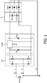
- K1 and K2 are input terminals for connection to a mains supply source.
- Diodes D1-D4 form a rectifier RB comprising rectifier output terminals.
- the rectifier output terminals are connected to respective converter input terminals of a DC-DC converter CONV for generating a DC-current out of the rectified mains supply voltage.
- the converter CONV comprises a first converter output terminal A and a second converter output terminal B.
- the converter input terminals are connected by means of a capacitor Cin and the first and second converter output terminals are connected by means of a capacitor Cout.
- Converter CONV is equipped with an input terminal K3 for receiving a control signal that activates or stops the operation of a converter control circuit comprised in the DC-DC converter and thereby, respectively, starts the operation of the LED light source or causes the LED light source to go into standby mode.
- the control signal can for instance be generated by light control circuitry in a lighting system of which the LED light source forms part.
- the DC-DC converter CONV may comprise one or more converter stages.
- the first stage may be a power factor correction (PFC) stage, matching the LED light source to the supplying mains, and one or more output stages, matching the converter to the LED load.
- PFC power factor correction
- the first converter output terminal A is connected to an anode of a LED load LL.
- the LED load LL is schematically represented by two LEDs, LED1 and LED2. In practice, the LED load will generally comprise a far higher number of LEDs.
- a cathode of the LED load LL is connected to the second converter output terminal B.
- the LED light source shown in Figure 1 is very suitable to be used in a luminaire.
- a luminaire is usually connected to a protective earth PE, which in turn is coupled to the "neutral" of the mains supply source.
- Coupling of the PE to the "neutral" of the mains supply source is not necessarily done through a direct connection as depicted in Figure 1 .
- Such coupling can be done at utility-grid level, or via a line filter capacitor such as a so-called "Y cap”.
- the LED load may couple with the luminaire and thus also with the protective earth PE by means of the parasitic capacitances schematically represented in Figure 1 as Cpar1, Cpar2 and Cpar3.
- the mains supply voltage is rectified by rectifier RB, and DC-DC converter CONV generates, out of the rectified mains supply voltage, a DC current that is supplied to the LED load LL. This DC current causes the LEDs to generate light.
- a first current flows from terminal K2 through parasitic capacitance Cpar3 and diode D3 to input terminal K1.
- a second current flows from input terminal K2, through Cpar2, LED2 and diode D3 to input terminal K1.
- a third current flows from terminal K2, through parasitic capacitance Cpar1, capacitor Cout and diode D3 to input terminal K1.
- a current flows from terminal K1, through diode D1 and capacitor Cin to converter output terminal B.
- a first current flows through capacitor Cout and parasitic capacitance Cpar1 to input terminal K2.
- a second current flows from converter output terminal B through capacitor Cout, LED1 and parasitic capacitance Cpar2 to input terminal K2.
- a third current flows from converter output terminal B through parasitic capacitance Cpar3 to terminal K2.
- the leakage current thus flows through the parasitic capacitances and also partly through the LEDs and thereby causes the LEDs to generate a small amount of light that is considered undesirable.
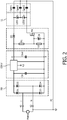
- the LED light source shown in Figure 2 is described in previously cited patent application WO 2013/132379 . It differs from the LED light source shown in Figure 1 in that the LED light source of Figure 2 further comprises resistors R1 and R2, diode D5, first controllable switch M1 and Zener diode Z1.
- the first controllable switch is a FET.
- the converter output terminals of DC-DC converter CONV are connected by means of a series arrangement of resistor R1 and resistor R2.
- a common terminal of resistor R1 and resistor R2 is connected to a control electrode of first controllable switch M1 and resistor R2 is shunted by Zener diode Z1.
- Resistor R1, resistor R2 and Zener diode Z1 together form first control circuitry for rendering the controllable switch M1 non-conductive in case the operation of the DC-DC converter is stopped and the LED light source is in standby mode.
- the operation of the DC-DC converter is stopped, the DC current supplying the LED load is no longer generated and the voltage between the converter output terminals decreases so that the first controllable switch M1 becomes non-conductive.
- Diode D5 and the body diode of controllable switch M1 block the leakage current, so that the parasitic capacitances are no longer charged and discharged, and the LEDs no longer generate a small amount of light, when the LED light source is in standby mode, so that the glow effect is effectively suppressed.
- the LEDs would still generate a small amount of light. This is because the LEDs would carry a reverse current flowing from their cathode to their anode for a high momentary magnitude of the mains voltage, when the voltage at terminal K2 is higher than the voltage at terminal K1. This current charges the parasitic capacitances. The LEDs would subsequently carry a current discharging the parasitic capacitances and flowing from their anode to their cathode in case the voltage at terminal K1 is higher than the voltage at terminal K2. In the embodiment shown in Figure 2 , the reverse current flowing through the LEDs is blocked by diode D5, acting as a first current control element.
- LED light source as illustrated in Figure 2 may still exhibit some glow effect under some circumstances, as explained in more detail hereinafter in reference to Figures 3 and 4 .
- Figure 3 illustrates a LED light source with an improved glow reduction circuit, in an exemplary embodiment of the invention.
- Figure 3 is substantially similar to Figure 2 , and most of the elements depicted in Figure 3 are introduced above in reference to Figure 2 .
- Figure 3 further discloses a typical line filter capacitor such as a so-called "Y capacitor" Ycap, which is a predominantly capacitive element that couples the drain electrode of the controllable switch M1 to PE.
- the controllable switch M1 itself has a parasitic capacitance, designated as Cpar in Figure 3 , between the drain electrode and the source electrode of controllable switch M1.
- the parasitic capacitance Cpar of the controllable switch M1 has been identified by the inventors as being the root cause for the flow of an undesirable current resulting in glow effect even during the non-conductive state of controllable switch M1.
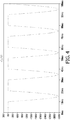
- Figure 4 shows the waveform of the voltage difference between the second output terminal B of converter CONV and PE.
- Cpar and Ycap form a capacitive divider for the voltage difference between the second output terminal B and PE.
- the remaining magnitude of the voltage difference between the drain of controllable switch M1 and PE can still be high enough to result in a current flowing through the LED load LL, likely to make the LED load emit glow light.
- the predominantly capacitive element may be coupled between the protective earth PE and a node coupling the first controllable switch M1 and the second current control element D, which has a beneficial technical effect of further improving glow current reduction.
- the current invention proposes that a second current control element is employed for blocking a current flowing from the first controllable switch M1 to the cathode of the LED load LL.
- the second current control element is preferably formed by a diode D, but may e.g. also be formed by a thyristor, sidac or Zener.
- the anode of diode D is electrically coupled to the cathode of the LED load LL, while the cathode of diode D is electrically coupled to the drain of the controllable switch M1.
- the technical function of the second current control element is that its parasitic capacitance that can be designated as CparD together with parasitic capacitance of the LED board Cpar3 forms a further capacitive divider of the voltage difference between the drain of controllable switch M1 and PE, such that only low ripple voltage remains on the LED board. If that ripple voltage is lower than the forward voltage of the LED load LL, then no visible glow light will be present.
- the first and the second current control elements are chosen to each have a parasitic capacitance smaller than the parasitic capacitance Cpar across controllable switch M1, that is: the capacitance between the source and the drain of the controllable switch M1.
- all the components of the LED light source may be implemented on a same Printed Circuit Board (PCB) substrate.
- PCB Printed Circuit Board
- the DC-DC converter CONV may be physically located on a first PCB, or so-called “driver PCB", while the LED load LL may be physically located on a second PCB, or "LED board” as referred to above.
- the first current control element D5 and/or the second current control element D may be physically implemented on either the first or the second PCB.
Landscapes
- Physics & Mathematics (AREA)
- Engineering & Computer Science (AREA)
- Microelectronics & Electronic Packaging (AREA)
- Optics & Photonics (AREA)
- Circuit Arrangement For Electric Light Sources In General (AREA)
- Led Devices (AREA)
Description
- The invention relates to the field of LED light sources. More in particular, the invention relates to LED light sources equipped with a standby function, in other words the operation of the LED light source can be stopped while the mains supply is still connected to it.
- Lighting systems based on LEDs are used on an increasing scale. LEDs have a high efficiency and a long life time. In many lighting systems, LEDs also offer a higher optical efficiency than other light sources. As a consequence, LEDs offer an interesting alternative for the well known light sources such as fluorescent lamps, high intensity discharge lamps or incandescent lamps.
- LED light sources are often comprised in a lighting system, wherein the operation of the LED light sources is controlled by control commands. Such control commands include commands for activating the LED light source and commands for stopping the operation of the LED light source, i.e. commands to start generating a LED current and commands to stop generating a LED current, respectively. In the latter case, operation is not stopped by interrupting the connection of the LED light source to the mains supply but by stopping for instance the operation of a converter circuit comprised in the LED light source. In this latter case, the LED light source is said to be in standby mode. In this standby mode, since the mains supply is still connected to the LED light source, the LED light source is still capable to receive further commands and process those commands. At the same time, however, the mains supply may cause a leakage current through parasitic capacitances and (part of) the LED load comprised in the LED light source. This leakage current can cause the LED string to generate a small amount of light resulting in a glow effect that is often undesirable.
- Published international patent application
WO 2013/132379 , commonly assigned herewith to the same applicant, relates to a LED light source allowing that during operation, a current supplying the LEDs can flow through a current control element and also through a first controllable switch that is maintained in the conductive state. In case the LED current supplied to the LED load by the converter is stopped, the LED light source is in a standby state and the first controllable switch is rendered non-conductive. As a result, leakage currents flowing from the mains supply to the LED load via parasitic capacitances are effectively suppressed, so that the LEDs do not generate a small amount of light during the standby state. However, surprisingly, the LED light source described inWO 2013/132379 cited above, may still suffer from undesirable glow effect during operation under certain conditions. - Notably, though such LED light source functions properly in combination with LED boards having a relatively low capacitance and with LED boards having a relatively high capacitance to protective earth, some glow effect may occur when such LED light source is combined with LED boards having a moderate parasitic capacitance.
- In the current disclosure, what will be referred to as a LED load may comprise one LED or a plurality of LEDs. When the LED load comprises a plurality of LEDs in a series arrangement, then what will be referred to as an anode of the LED load will be the anode of the first LED in the series arrangement that is to be flowed through with current, and what will be referred to as a cathode of the LED load will be the cathode of the last LED in the series arrangement that is to be flowed through with current. Similarly, when the LED load comprises a plurality of LEDs in a parallel arrangement, with possibly a plurality of parallel branches each comprising a plurality of LED arranged in series, then what will be referred to as an anode of such an arrangement will be the electrical node that is of the same potential as the anodes of the first LEDs of each parallel branch to be flowed through with current, while what will be referred to as a cathode of such an arrangement will be the electrical node that is of the same potential as the cathodes of the last LED in each parallel branch to be flowed through with current. In other words, the anode of the LED load will be considered as the most positive node thereof, while the cathode will be considered as the most negative node.
- It is an object of the invention to provide a LED light source having an improved glow reduction, notably in comparison with the LED light source described in
WO 2013/132379 cited above. - According to a first aspect of the invention, a LED light source is provided, comprising:
- input terminals for connection to a mains voltage supply source,
- a rectifier coupled to the input terminals for rectifying the mains supply voltage supplied by the mains supply voltage source and comprising rectifier output terminals,
- a DC-DC converter for generating a DC current out of the rectified mains supply voltage, comprising converter input terminals connected to the rectifier output terminals and comprising a first converter output terminal and a second converter output terminal,
- a LED load comprising one or more LEDs and having an anode as its most positive node and a cathode as its most negative node , the anode of the LED load being coupled to the first converter output terminal via a first current control element for blocking a current flowing from the anode of the LED load to the first converter output terminal, and the cathode of the LED load being coupled to the second converter output terminal via a first controllable switch having a control electrode coupled to first control circuitry for rendering the controllable switch non-conductive in case the LED light source is in standby mode, whereby the cathode of the LED load is coupled to the first controllable switch via a second current control element for blocking a current flowing from the first controllable switch to the cathode of the LED load.
- Thus, the first current control element and the second control element do not allow any undesirable current to flow through the load, which would be likely to result in glow effect, whatever the used configuration of the LED board.
- In accordance with a further aspect of the invention, the second current control element can comprise a diode.
- In accordance with a further aspect of the invention, the first current control element can comprise a diode.
- In a further embodiment of the invention, the LED light source can be provided with a protective earth terminal PE, and a predominantly capacitive element coupled between the protective earth terminal PE and a node coupling the first controllable switch and the second current control element.
- In a further embodiment of the invention, at least the DC-DC converter can be located on a first PCB, the first current control element and/or the second current control element being located on said first PCB.
- In a further embodiment of the invention, at least the LED load can be located on a second PCB, the first control element and/or the second current control element being located on said second PCB.
- In a further embodiment of the invention, the first and second current control elements can each have a parasitic capacitance that is smaller than the parasitic capacitance across the first controllable switch.
- These and other characteristics and advantages of the invention will be made clearer in view of the detailed description given below of preferred embodiments, provided by way of an illustrative and non-limiting example only, as well as the accompanying drawings which represent:
-
Figure 1 , a LED light source known in the prior art, that does not comprise a glow reduction circuit; -
Figure 2 , a LED light source comprising a glow reduction circuit, known in the prior art; -
Figure 3 , a LED light source with an improved glow reduction circuit, in an exemplary embodiment of the invention; -
Figure 4 , a diagram depicting a voltage waveform resulting from a parasitic capacitance in a LED light source comprising a glow reduction circuit as illustrated byFigure 2 . - In
Figure 1 , K1 and K2 are input terminals for connection to a mains supply source. Diodes D1-D4 form a rectifier RB comprising rectifier output terminals. The rectifier output terminals are connected to respective converter input terminals of a DC-DC converter CONV for generating a DC-current out of the rectified mains supply voltage. The converter CONV comprises a first converter output terminal A and a second converter output terminal B. The converter input terminals are connected by means of a capacitor Cin and the first and second converter output terminals are connected by means of a capacitor Cout. - Converter CONV is equipped with an input terminal K3 for receiving a control signal that activates or stops the operation of a converter control circuit comprised in the DC-DC converter and thereby, respectively, starts the operation of the LED light source or causes the LED light source to go into standby mode. The control signal can for instance be generated by light control circuitry in a lighting system of which the LED light source forms part.
- The DC-DC converter CONV may comprise one or more converter stages. In case the DC-DC converter comprises multiple stages, the first stage may be a power factor correction (PFC) stage, matching the LED light source to the supplying mains, and one or more output stages, matching the converter to the LED load.
- The first converter output terminal A is connected to an anode of a LED load LL. In
Figure 1 , the LED load LL is schematically represented by two LEDs, LED1 and LED2. In practice, the LED load will generally comprise a far higher number of LEDs. A cathode of the LED load LL is connected to the second converter output terminal B. - The LED light source shown in
Figure 1 is very suitable to be used in a luminaire. For safety reasons such a luminaire is usually connected to a protective earth PE, which in turn is coupled to the "neutral" of the mains supply source. Coupling of the PE to the "neutral" of the mains supply source is not necessarily done through a direct connection as depicted inFigure 1 . Such coupling can be done at utility-grid level, or via a line filter capacitor such as a so-called "Y cap". The LED load may couple with the luminaire and thus also with the protective earth PE by means of the parasitic capacitances schematically represented inFigure 1 as Cpar1, Cpar2 and Cpar3. - During normal operation of the LED light source shown in
Figure 1 , the mains supply voltage is rectified by rectifier RB, and DC-DC converter CONV generates, out of the rectified mains supply voltage, a DC current that is supplied to the LED load LL. This DC current causes the LEDs to generate light. - However, in case a control signal that stops the operation of the DC-DC converter is received at terminal K3, the DC current that flows through the LEDs is no longer generated and the LED light source is in standby mode.
- Since the input terminals of the LED light source are still connected to the mains supply source, the parasitic capacitances coupling the protective earth to the LED load cause an AC leakage current to flow.
- During a first part of the mains cycle, a first current flows from terminal K2 through parasitic capacitance Cpar3 and diode D3 to input terminal K1. A second current flows from input terminal K2, through Cpar2, LED2 and diode D3 to input terminal K1. A third current flows from terminal K2, through parasitic capacitance Cpar1, capacitor Cout and diode D3 to input terminal K1.These currents charge the parasitic capacitances.
- During a second part of the mains cycle, a current flows from terminal K1, through diode D1 and capacitor Cin to converter output terminal B. From converter output terminal B a first current flows through capacitor Cout and parasitic capacitance Cpar1 to input terminal K2. A second current flows from converter output terminal B through capacitor Cout, LED1 and parasitic capacitance Cpar2 to input terminal K2. A third current flows from converter output terminal B through parasitic capacitance Cpar3 to terminal K2. These currents discharge the parasitic capacitances.
- The leakage current thus flows through the parasitic capacitances and also partly through the LEDs and thereby causes the LEDs to generate a small amount of light that is considered undesirable.
- The LED light source shown in
Figure 2 is described in previously cited patent applicationWO 2013/132379 . It differs from the LED light source shown inFigure 1 in that the LED light source ofFigure 2 further comprises resistors R1 and R2, diode D5, first controllable switch M1 and Zener diode Z1. In the embodiment shown inFigure 2 , the first controllable switch is a FET. The converter output terminals of DC-DC converter CONV are connected by means of a series arrangement of resistor R1 and resistor R2. A common terminal of resistor R1 and resistor R2 is connected to a control electrode of first controllable switch M1 and resistor R2 is shunted by Zener diode Z1. Resistor R1, resistor R2 and Zener diode Z1 together form first control circuitry for rendering the controllable switch M1 non-conductive in case the operation of the DC-DC converter is stopped and the LED light source is in standby mode. - During normal operation of the LED light source shown in
Figure 2 , the voltage across capacitor Cout and thus across the series arrangement of resistor R1 and resistor R2 is high enough to maintain the first controllable switch M1 in a conductive state. As a consequence, the normal operation of the LED light source shown inFigure 2 is very similar to the normal operation of the prior art LED light source shown inFigure 1 , since the diode D5 and the controllable switch M1 conduct the DC current generated by the DC-DC converter CONV. - In case the DC-DC converter receives a control signal at its terminal K3 to change from normal operation to standby mode, the operation of the DC-DC converter is stopped, the DC current supplying the LED load is no longer generated and the voltage between the converter output terminals decreases so that the first controllable switch M1 becomes non-conductive. Diode D5 and the body diode of controllable switch M1 block the leakage current, so that the parasitic capacitances are no longer charged and discharged, and the LEDs no longer generate a small amount of light, when the LED light source is in standby mode, so that the glow effect is effectively suppressed.
- It is noted that in case the diode D5 were dispensed with, the LEDs would still generate a small amount of light. This is because the LEDs would carry a reverse current flowing from their cathode to their anode for a high momentary magnitude of the mains voltage, when the voltage at terminal K2 is higher than the voltage at terminal K1. This current charges the parasitic capacitances. The LEDs would subsequently carry a current discharging the parasitic capacitances and flowing from their anode to their cathode in case the voltage at terminal K1 is higher than the voltage at terminal K2. In the embodiment shown in
Figure 2 , the reverse current flowing through the LEDs is blocked by diode D5, acting as a first current control element. - However a LED light source as illustrated in
Figure 2 may still exhibit some glow effect under some circumstances, as explained in more detail hereinafter in reference toFigures 3 and4 . -
Figure 3 illustrates a LED light source with an improved glow reduction circuit, in an exemplary embodiment of the invention.Figure 3 is substantially similar toFigure 2 , and most of the elements depicted inFigure 3 are introduced above in reference toFigure 2 . In contrast toFigure 2 ,Figure 3 further discloses a typical line filter capacitor such as a so-called "Y capacitor" Ycap, which is a predominantly capacitive element that couples the drain electrode of the controllable switch M1 to PE. Furthermore, the controllable switch M1 itself has a parasitic capacitance, designated as Cpar inFigure 3 , between the drain electrode and the source electrode of controllable switch M1. The parasitic capacitance Cpar of the controllable switch M1 has been identified by the inventors as being the root cause for the flow of an undesirable current resulting in glow effect even during the non-conductive state of controllable switch M1.Figure 4 shows the waveform of the voltage difference between the second output terminal B of converter CONV and PE. Cpar and Ycap form a capacitive divider for the voltage difference between the second output terminal B and PE. However, the remaining magnitude of the voltage difference between the drain of controllable switch M1 and PE can still be high enough to result in a current flowing through the LED load LL, likely to make the LED load emit glow light. As depicted inFigure 3 , the predominantly capacitive element may be coupled between the protective earth PE and a node coupling the first controllable switch M1 and the second current control element D, which has a beneficial technical effect of further improving glow current reduction. - The current invention proposes that a second current control element is employed for blocking a current flowing from the first controllable switch M1 to the cathode of the LED load LL. In the exemplary embodiment illustrated by
Figure 3 , the second current control element is preferably formed by a diode D, but may e.g. also be formed by a thyristor, sidac or Zener. The anode of diode D is electrically coupled to the cathode of the LED load LL, while the cathode of diode D is electrically coupled to the drain of the controllable switch M1. - The technical function of the second current control element is that its parasitic capacitance that can be designated as CparD together with parasitic capacitance of the LED board Cpar3 forms a further capacitive divider of the voltage difference between the drain of controllable switch M1 and PE, such that only low ripple voltage remains on the LED board. If that ripple voltage is lower than the forward voltage of the LED load LL, then no visible glow light will be present. Preferably, the first and the second current control elements are chosen to each have a parasitic capacitance smaller than the parasitic capacitance Cpar across controllable switch M1, that is: the capacitance between the source and the drain of the controllable switch M1.
- In some embodiments, all the components of the LED light source may be implemented on a same Printed Circuit Board (PCB) substrate.
- In other exemplary embodiments, the DC-DC converter CONV, and possibly the rectifier RB, as well as the capacitors Cin and Cout, may be physically located on a first PCB, or so-called "driver PCB", while the LED load LL may be physically located on a second PCB, or "LED board" as referred to above. The first current control element D5 and/or the second current control element D may be physically implemented on either the first or the second PCB.
- While the invention has been illustrated and described in detail in the drawings and foregoing description, such illustration and description are to be considered illustrative or exemplary and not restrictive; the invention is not limited to the disclosed embodiments. Other variations to the disclosed embodiments can be understood and effected by those skilled in the art in practicing the claimed invention, from a study of the drawings, the disclosure, and the appended claims. In the claims, the word "comprising" does not exclude other elements or steps, and the indefinite article "a" or "an" does not exclude a plurality. The mere fact that certain measures are recited in mutually different dependent claims does not indicate that a combination of these measures cannot be used to advantage. Any reference signs in the claims should not be construed as limiting the scope.
Claims (7)
- A LED light source comprising:- input terminals (K1, K2) for connection to a mains voltage supply source,- a rectifier (RB) coupled to the input terminals for rectifying the mains supply voltage supplied by the mains supply voltage source and comprising rectifier output terminals,- a DC-DC converter (CONV) for generating a DC current out of the rectified mains supply voltage, comprising converter input terminals connected to the rectifier output terminals and comprising a first converter output terminal (A) and a second converter output terminal (B),- a LED load (LL) comprising one or more LEDs and having an anode as its most positive node and a cathode as its most negative node,the anode being coupled to the first converter output terminal via a first current control element (D5) for blocking a current flowing from the anode of the LED load to the first converter output terminal, and the cathode being coupled to the second converter output terminal via a first controllable switch (M1) having a control electrode coupled to first control circuitry for rendering the controllable switch non-conductive in case the LED light source is in standby mode, characterised in that the cathode of the LED load is coupled to the first controllable switch (M1) via a second current control element (D) for blocking a current flowing from the first controllable switch (M1) to the cathode of LED load.
- A LED light source as claimed in Claim 1, wherein the second current control element (D) comprises a diode.
- A LED light source as claimed in any of previous claims, wherein the first current control element (D5) comprises a diode.
- A LED light source as claimed in any of previous claims, wherein the LED light source is provided with a protective earth terminal (PE), and a predominantly capacitive element (Ycap) is coupled between the protective earth terminal (PE) and a node coupling the first controllable switch (M1) and the second current control element (D).
- A LED light source as claimed in any of previous claims, wherein at least the DC-DC converter (CONV) is located on a first PCB, the first current control element (D5) and/or the second current control element (D) being located on said first PCB.
- A LED light source as claimed in any of Claims 1 to 3, wherein at least the LED load (LL) is located on a second PCB, the first control element (D5) and/or the second current control element (D) being located on said second PCB.
- A LED light source as claimed in any of the previous claims, wherein the first and second current control elements (D5, D) are each selected to have a parasitic capacitance that is smaller than the parasitic capacitance (Cpar) across the first controllable switch (M1).
Priority Applications (1)
| Application Number | Priority Date | Filing Date | Title |
|---|---|---|---|
| PL16170050T PL3102003T3 (en) | 2015-06-04 | 2016-05-18 | Led light source with improved glow reduction |
Applications Claiming Priority (1)
| Application Number | Priority Date | Filing Date | Title |
|---|---|---|---|
| EP15170629 | 2015-06-04 |
Publications (2)
| Publication Number | Publication Date |
|---|---|
| EP3102003A1 EP3102003A1 (en) | 2016-12-07 |
| EP3102003B1 true EP3102003B1 (en) | 2017-08-16 |
Family
ID=53284104
Family Applications (1)
| Application Number | Title | Priority Date | Filing Date |
|---|---|---|---|
| EP16170050.5A Active EP3102003B1 (en) | 2015-06-04 | 2016-05-18 | Led light source with improved glow reduction |
Country Status (8)
| Country | Link |
|---|---|
| US (1) | US9967935B2 (en) |
| EP (1) | EP3102003B1 (en) |
| JP (1) | JP6353992B1 (en) |
| CN (1) | CN107710872B (en) |
| ES (1) | ES2644863T3 (en) |
| PL (1) | PL3102003T3 (en) |
| RU (1) | RU2713922C2 (en) |
| WO (1) | WO2016192987A1 (en) |
Families Citing this family (3)
| Publication number | Priority date | Publication date | Assignee | Title |
|---|---|---|---|---|
| DE102015101086B4 (en) * | 2015-01-26 | 2018-04-12 | Infineon Technologies Ag | SEMICONDUCTOR POWER MODULE ARRANGEMENT |
| WO2023104614A1 (en) * | 2021-12-07 | 2023-06-15 | Signify Holding B.V. | Lighting assembly |
| WO2024179819A1 (en) | 2023-03-02 | 2024-09-06 | Signify Holding B.V. | An led module |
Family Cites Families (19)
| Publication number | Priority date | Publication date | Assignee | Title |
|---|---|---|---|---|
| WO2007016373A2 (en) * | 2005-07-28 | 2007-02-08 | Synditec, Inc. | Pulsed current averaging controller with amplitude modulation and time division multiplexing for arrays of independent pluralities of light emitting diodes |
| US8742674B2 (en) * | 2006-01-20 | 2014-06-03 | Point Somee Limited Liability Company | Adaptive current regulation for solid state lighting |
| TW200820166A (en) * | 2006-10-27 | 2008-05-01 | Beyond Innovation Tech Co Ltd | Driving device and switching circuit thereof |
| US7675761B2 (en) * | 2007-06-01 | 2010-03-09 | Power Integrations, Inc. | Method and apparatus to control two regulated outputs of a flyback power supply |
| US8729870B2 (en) * | 2008-08-15 | 2014-05-20 | Analog Modules, Inc. | Biphase laser diode driver and method |
| EP2510749B1 (en) * | 2009-12-11 | 2013-09-25 | Koninklijke Philips N.V. | Driving modes for light circuits |
| US20120256550A1 (en) * | 2009-12-22 | 2012-10-11 | Takashi Akiyama | Led driving circuit |
| GB201011081D0 (en) * | 2010-07-01 | 2010-08-18 | Macfarlane Alistair | Improved semi resonant switching regulator, power factor control and LED lighting |
| EP2634823B1 (en) * | 2010-10-28 | 2019-05-08 | Citizen Watch Co., Ltd. | Led lighting circuit, led illuminating device, and socket for led illuminating unit |
| WO2013027171A1 (en) * | 2011-08-23 | 2013-02-28 | Koninklijke Philips Electronics N.V. | Led light source |
| US9253831B2 (en) * | 2011-11-04 | 2016-02-02 | Koninklijke Philips N.V. | Driver device and driving method for driving a load, in particular an led unit |
| US20130163270A1 (en) * | 2011-12-22 | 2013-06-27 | Seth Burgin | Elevator cabin lighting with integrated emergency lighting |
| PL2823691T3 (en) * | 2012-03-09 | 2019-09-30 | Signify Holding B.V. | Led light source |
| DE102013201439A1 (en) * | 2012-05-04 | 2013-11-07 | Osram Gmbh | Circuit arrangement for operating at least a first and a second cascade of LEDs |
| WO2014085837A2 (en) * | 2012-12-06 | 2014-06-12 | Tridonic Gmbh & Co Kg | Operating device for illuminant |
| US9093894B2 (en) * | 2012-12-17 | 2015-07-28 | Greenmark Technology Inc. | Multiple-level power control system |
| US8829819B1 (en) * | 2013-05-07 | 2014-09-09 | Power Integrations, Inc. | Enhanced active preload for high performance LED driver with extended dimming |
| US9538623B2 (en) * | 2014-05-12 | 2017-01-03 | Lg Electronics Inc. | Lighting device |
| US20160088702A1 (en) * | 2014-09-24 | 2016-03-24 | Richard Landry Gray | Devices for LED Direct Driver |
-
2016
- 2016-05-18 JP JP2017562769A patent/JP6353992B1/en active Active
- 2016-05-18 PL PL16170050T patent/PL3102003T3/en unknown
- 2016-05-18 EP EP16170050.5A patent/EP3102003B1/en active Active
- 2016-05-18 RU RU2017146373A patent/RU2713922C2/en active
- 2016-05-18 ES ES16170050.5T patent/ES2644863T3/en active Active
- 2016-05-18 WO PCT/EP2016/061061 patent/WO2016192987A1/en active Application Filing
- 2016-05-18 CN CN201680032200.2A patent/CN107710872B/en active Active
- 2016-05-23 US US15/161,370 patent/US9967935B2/en active Active
Non-Patent Citations (1)
| Title |
|---|
| None * |
Also Published As
| Publication number | Publication date |
|---|---|
| US20160360588A1 (en) | 2016-12-08 |
| PL3102003T3 (en) | 2018-01-31 |
| JP6353992B1 (en) | 2018-07-04 |
| RU2713922C2 (en) | 2020-02-11 |
| CN107710872B (en) | 2019-11-22 |
| JP2018520471A (en) | 2018-07-26 |
| US9967935B2 (en) | 2018-05-08 |
| WO2016192987A1 (en) | 2016-12-08 |
| RU2017146373A3 (en) | 2019-12-12 |
| RU2017146373A (en) | 2019-07-09 |
| CN107710872A (en) | 2018-02-16 |
| ES2644863T3 (en) | 2017-11-30 |
| EP3102003A1 (en) | 2016-12-07 |
Similar Documents
| Publication | Publication Date | Title |
|---|---|---|
| EP2914065B1 (en) | Illumination lamp and illumination apparatus | |
| EP2823691B1 (en) | Led light source | |
| JP5498240B2 (en) | Light source module, lighting device, and lighting apparatus using the same | |
| US8847497B2 (en) | Driving modes for light circuits | |
| EP3102003B1 (en) | Led light source with improved glow reduction | |
| US20130342115A1 (en) | Light-emitting device | |
| CN111212497A (en) | Driving circuit | |
| JP2017513184A (en) | Fluorescent lamp compatible type LED lighting device and electric shock protection device therefor | |
| JP2016006761A (en) | Led driver | |
| US11172551B2 (en) | Solid-state lighting with a driver controllable by a power-line dimmer | |
| CN210351736U (en) | Low-frequency-flash high-power-factor driving circuit | |
| US10219332B2 (en) | Constant-current constant-voltage (CCCV) control unit power supply | |
| US20160205738A1 (en) | Led tube adapted for use with electronic ballast or ac mains and controlling method thereof | |
| KR102654416B1 (en) | light emitting diode lighting device | |
| KR20140049841A (en) | Apparatus and method for supplying power of led lighting, and led lighting apparatus using that | |
| CN110999538B (en) | LED light source and LED lamp | |
| KR101597773B1 (en) | Power saving device og LED lighting fixtures | |
| JP2017174680A (en) | LED lamp and LED lighting device | |
| KR101382708B1 (en) | Power supply circuit | |
| KR101219993B1 (en) | Power supply apparatus | |
| JP2017120732A (en) | Light-emitting device |
Legal Events
| Date | Code | Title | Description |
|---|---|---|---|
| PUAI | Public reference made under article 153(3) epc to a published international application that has entered the european phase |
Free format text: ORIGINAL CODE: 0009012 |
|
| 17P | Request for examination filed |
Effective date: 20160929 |
|
| AK | Designated contracting states |
Kind code of ref document: A1 Designated state(s): AL AT BE BG CH CY CZ DE DK EE ES FI FR GB GR HR HU IE IS IT LI LT LU LV MC MK MT NL NO PL PT RO RS SE SI SK SM TR |
|
| AX | Request for extension of the european patent |
Extension state: BA ME |
|
| GRAP | Despatch of communication of intention to grant a patent |
Free format text: ORIGINAL CODE: EPIDOSNIGR1 |
|
| INTG | Intention to grant announced |
Effective date: 20170303 |
|
| GRAS | Grant fee paid |
Free format text: ORIGINAL CODE: EPIDOSNIGR3 |
|
| GRAA | (expected) grant |
Free format text: ORIGINAL CODE: 0009210 |
|
| RBV | Designated contracting states (corrected) |
Designated state(s): AL AT BE BG CH CY CZ DE DK EE ES FI FR GB GR HR HU IE IS IT LI LT LU LV MC MK MT NL NO PL PT RO RS SE SI SK SM TR |
|
| RIN1 | Information on inventor provided before grant (corrected) |
Inventor name: HULSHOF, FOKKO, JAN, WILLEM |
|
| AK | Designated contracting states |
Kind code of ref document: B1 Designated state(s): AL AT BE BG CH CY CZ DE DK EE ES FI FR GB GR HR HU IE IS IT LI LT LU LV MC MK MT NL NO PL PT RO RS SE SI SK SM TR |
|
| REG | Reference to a national code |
Ref country code: GB Ref legal event code: FG4D |
|
| REG | Reference to a national code |
Ref country code: CH Ref legal event code: EP |
|
| REG | Reference to a national code |
Ref country code: IE Ref legal event code: FG4D |
|
| REG | Reference to a national code |
Ref country code: AT Ref legal event code: REF Ref document number: 920247 Country of ref document: AT Kind code of ref document: T Effective date: 20170915 |
|
| REG | Reference to a national code |
Ref country code: DE Ref legal event code: R096 Ref document number: 602016000239 Country of ref document: DE |
|
| REG | Reference to a national code |
Ref country code: ES Ref legal event code: FG2A Ref document number: 2644863 Country of ref document: ES Kind code of ref document: T3 Effective date: 20171130 |
|
| REG | Reference to a national code |
Ref country code: NL Ref legal event code: MP Effective date: 20170816 |
|
| REG | Reference to a national code |
Ref country code: LT Ref legal event code: MG4D |
|
| REG | Reference to a national code |
Ref country code: AT Ref legal event code: MK05 Ref document number: 920247 Country of ref document: AT Kind code of ref document: T Effective date: 20170816 |
|
| PG25 | Lapsed in a contracting state [announced via postgrant information from national office to epo] |
Ref country code: FI Free format text: LAPSE BECAUSE OF FAILURE TO SUBMIT A TRANSLATION OF THE DESCRIPTION OR TO PAY THE FEE WITHIN THE PRESCRIBED TIME-LIMIT Effective date: 20170816 Ref country code: NL Free format text: LAPSE BECAUSE OF FAILURE TO SUBMIT A TRANSLATION OF THE DESCRIPTION OR TO PAY THE FEE WITHIN THE PRESCRIBED TIME-LIMIT Effective date: 20170816 Ref country code: LT Free format text: LAPSE BECAUSE OF FAILURE TO SUBMIT A TRANSLATION OF THE DESCRIPTION OR TO PAY THE FEE WITHIN THE PRESCRIBED TIME-LIMIT Effective date: 20170816 Ref country code: AT Free format text: LAPSE BECAUSE OF FAILURE TO SUBMIT A TRANSLATION OF THE DESCRIPTION OR TO PAY THE FEE WITHIN THE PRESCRIBED TIME-LIMIT Effective date: 20170816 Ref country code: SE Free format text: LAPSE BECAUSE OF FAILURE TO SUBMIT A TRANSLATION OF THE DESCRIPTION OR TO PAY THE FEE WITHIN THE PRESCRIBED TIME-LIMIT Effective date: 20170816 Ref country code: NO Free format text: LAPSE BECAUSE OF FAILURE TO SUBMIT A TRANSLATION OF THE DESCRIPTION OR TO PAY THE FEE WITHIN THE PRESCRIBED TIME-LIMIT Effective date: 20171116 |
|
| PG25 | Lapsed in a contracting state [announced via postgrant information from national office to epo] |
Ref country code: BG Free format text: LAPSE BECAUSE OF FAILURE TO SUBMIT A TRANSLATION OF THE DESCRIPTION OR TO PAY THE FEE WITHIN THE PRESCRIBED TIME-LIMIT Effective date: 20171116 Ref country code: GR Free format text: LAPSE BECAUSE OF FAILURE TO SUBMIT A TRANSLATION OF THE DESCRIPTION OR TO PAY THE FEE WITHIN THE PRESCRIBED TIME-LIMIT Effective date: 20171117 Ref country code: LV Free format text: LAPSE BECAUSE OF FAILURE TO SUBMIT A TRANSLATION OF THE DESCRIPTION OR TO PAY THE FEE WITHIN THE PRESCRIBED TIME-LIMIT Effective date: 20170816 Ref country code: RS Free format text: LAPSE BECAUSE OF FAILURE TO SUBMIT A TRANSLATION OF THE DESCRIPTION OR TO PAY THE FEE WITHIN THE PRESCRIBED TIME-LIMIT Effective date: 20170816 Ref country code: IS Free format text: LAPSE BECAUSE OF FAILURE TO SUBMIT A TRANSLATION OF THE DESCRIPTION OR TO PAY THE FEE WITHIN THE PRESCRIBED TIME-LIMIT Effective date: 20171216 |
|
| PG25 | Lapsed in a contracting state [announced via postgrant information from national office to epo] |
Ref country code: DK Free format text: LAPSE BECAUSE OF FAILURE TO SUBMIT A TRANSLATION OF THE DESCRIPTION OR TO PAY THE FEE WITHIN THE PRESCRIBED TIME-LIMIT Effective date: 20170816 Ref country code: CZ Free format text: LAPSE BECAUSE OF FAILURE TO SUBMIT A TRANSLATION OF THE DESCRIPTION OR TO PAY THE FEE WITHIN THE PRESCRIBED TIME-LIMIT Effective date: 20170816 |
|
| REG | Reference to a national code |
Ref country code: DE Ref legal event code: R097 Ref document number: 602016000239 Country of ref document: DE |
|
| REG | Reference to a national code |
Ref country code: FR Ref legal event code: PLFP Year of fee payment: 3 |
|
| PG25 | Lapsed in a contracting state [announced via postgrant information from national office to epo] |
Ref country code: SK Free format text: LAPSE BECAUSE OF FAILURE TO SUBMIT A TRANSLATION OF THE DESCRIPTION OR TO PAY THE FEE WITHIN THE PRESCRIBED TIME-LIMIT Effective date: 20170816 Ref country code: SM Free format text: LAPSE BECAUSE OF FAILURE TO SUBMIT A TRANSLATION OF THE DESCRIPTION OR TO PAY THE FEE WITHIN THE PRESCRIBED TIME-LIMIT Effective date: 20170816 Ref country code: EE Free format text: LAPSE BECAUSE OF FAILURE TO SUBMIT A TRANSLATION OF THE DESCRIPTION OR TO PAY THE FEE WITHIN THE PRESCRIBED TIME-LIMIT Effective date: 20170816 |
|
| PLBE | No opposition filed within time limit |
Free format text: ORIGINAL CODE: 0009261 |
|
| STAA | Information on the status of an ep patent application or granted ep patent |
Free format text: STATUS: NO OPPOSITION FILED WITHIN TIME LIMIT |
|
| 26N | No opposition filed |
Effective date: 20180517 |
|
| PG25 | Lapsed in a contracting state [announced via postgrant information from national office to epo] |
Ref country code: SI Free format text: LAPSE BECAUSE OF FAILURE TO SUBMIT A TRANSLATION OF THE DESCRIPTION OR TO PAY THE FEE WITHIN THE PRESCRIBED TIME-LIMIT Effective date: 20170816 |
|
| REG | Reference to a national code |
Ref country code: BE Ref legal event code: MM Effective date: 20180531 |
|
| PG25 | Lapsed in a contracting state [announced via postgrant information from national office to epo] |
Ref country code: MC Free format text: LAPSE BECAUSE OF FAILURE TO SUBMIT A TRANSLATION OF THE DESCRIPTION OR TO PAY THE FEE WITHIN THE PRESCRIBED TIME-LIMIT Effective date: 20170816 |
|
| REG | Reference to a national code |
Ref country code: IE Ref legal event code: MM4A |
|
| PG25 | Lapsed in a contracting state [announced via postgrant information from national office to epo] |
Ref country code: LU Free format text: LAPSE BECAUSE OF NON-PAYMENT OF DUE FEES Effective date: 20180518 |
|
| PG25 | Lapsed in a contracting state [announced via postgrant information from national office to epo] |
Ref country code: IE Free format text: LAPSE BECAUSE OF NON-PAYMENT OF DUE FEES Effective date: 20180518 |
|
| PG25 | Lapsed in a contracting state [announced via postgrant information from national office to epo] |
Ref country code: BE Free format text: LAPSE BECAUSE OF NON-PAYMENT OF DUE FEES Effective date: 20180531 |
|
| REG | Reference to a national code |
Ref country code: DE Ref legal event code: R079 Ref document number: 602016000239 Country of ref document: DE Free format text: PREVIOUS MAIN CLASS: H05B0033080000 Ipc: H05B0045000000 |
|
| REG | Reference to a national code |
Ref country code: CH Ref legal event code: PL |
|
| PG25 | Lapsed in a contracting state [announced via postgrant information from national office to epo] |
Ref country code: LI Free format text: LAPSE BECAUSE OF NON-PAYMENT OF DUE FEES Effective date: 20190531 Ref country code: CH Free format text: LAPSE BECAUSE OF NON-PAYMENT OF DUE FEES Effective date: 20190531 Ref country code: MT Free format text: LAPSE BECAUSE OF NON-PAYMENT OF DUE FEES Effective date: 20180518 |
|
| PG25 | Lapsed in a contracting state [announced via postgrant information from national office to epo] |
Ref country code: TR Free format text: LAPSE BECAUSE OF FAILURE TO SUBMIT A TRANSLATION OF THE DESCRIPTION OR TO PAY THE FEE WITHIN THE PRESCRIBED TIME-LIMIT Effective date: 20170816 |
|
| PG25 | Lapsed in a contracting state [announced via postgrant information from national office to epo] |
Ref country code: PT Free format text: LAPSE BECAUSE OF FAILURE TO SUBMIT A TRANSLATION OF THE DESCRIPTION OR TO PAY THE FEE WITHIN THE PRESCRIBED TIME-LIMIT Effective date: 20170816 |
|
| PG25 | Lapsed in a contracting state [announced via postgrant information from national office to epo] |
Ref country code: HR Free format text: LAPSE BECAUSE OF FAILURE TO SUBMIT A TRANSLATION OF THE DESCRIPTION OR TO PAY THE FEE WITHIN THE PRESCRIBED TIME-LIMIT Effective date: 20170816 Ref country code: CY Free format text: LAPSE BECAUSE OF FAILURE TO SUBMIT A TRANSLATION OF THE DESCRIPTION OR TO PAY THE FEE WITHIN THE PRESCRIBED TIME-LIMIT Effective date: 20170816 Ref country code: HU Free format text: LAPSE BECAUSE OF FAILURE TO SUBMIT A TRANSLATION OF THE DESCRIPTION OR TO PAY THE FEE WITHIN THE PRESCRIBED TIME-LIMIT; INVALID AB INITIO Effective date: 20160518 Ref country code: MK Free format text: LAPSE BECAUSE OF NON-PAYMENT OF DUE FEES Effective date: 20170816 Ref country code: RO Free format text: LAPSE BECAUSE OF FAILURE TO SUBMIT A TRANSLATION OF THE DESCRIPTION OR TO PAY THE FEE WITHIN THE PRESCRIBED TIME-LIMIT Effective date: 20170816 |
|
| PG25 | Lapsed in a contracting state [announced via postgrant information from national office to epo] |
Ref country code: AL Free format text: LAPSE BECAUSE OF FAILURE TO SUBMIT A TRANSLATION OF THE DESCRIPTION OR TO PAY THE FEE WITHIN THE PRESCRIBED TIME-LIMIT Effective date: 20170816 |
|
| REG | Reference to a national code |
Ref country code: DE Ref legal event code: R081 Ref document number: 602016000239 Country of ref document: DE Owner name: SIGNIFY HOLDING B.V., NL Free format text: FORMER OWNER: PHILIPS LIGHTING HOLDING B.V., EINDHOVEN, NL |
|
| P01 | Opt-out of the competence of the unified patent court (upc) registered |
Effective date: 20230425 |
|
| PGFP | Annual fee paid to national office [announced via postgrant information from national office to epo] |
Ref country code: IT Payment date: 20230525 Year of fee payment: 8 |
|
| PGFP | Annual fee paid to national office [announced via postgrant information from national office to epo] |
Ref country code: DE Payment date: 20230726 Year of fee payment: 8 |
|
| PGFP | Annual fee paid to national office [announced via postgrant information from national office to epo] |
Ref country code: GB Payment date: 20240521 Year of fee payment: 9 |
|
| PGFP | Annual fee paid to national office [announced via postgrant information from national office to epo] |
Ref country code: ES Payment date: 20240610 Year of fee payment: 9 |
|
| PGFP | Annual fee paid to national office [announced via postgrant information from national office to epo] |
Ref country code: FR Payment date: 20240527 Year of fee payment: 9 |
|
| PGFP | Annual fee paid to national office [announced via postgrant information from national office to epo] |
Ref country code: PL Payment date: 20240508 Year of fee payment: 9 |