EP3101791A2 - Control power supply device for inverter - Google Patents
Control power supply device for inverter Download PDFInfo
- Publication number
- EP3101791A2 EP3101791A2 EP16169363.5A EP16169363A EP3101791A2 EP 3101791 A2 EP3101791 A2 EP 3101791A2 EP 16169363 A EP16169363 A EP 16169363A EP 3101791 A2 EP3101791 A2 EP 3101791A2
- Authority
- EP
- European Patent Office
- Prior art keywords
- smps
- controller
- inverter
- voltage
- main
- Prior art date
- Legal status (The legal status is an assumption and is not a legal conclusion. Google has not performed a legal analysis and makes no representation as to the accuracy of the status listed.)
- Granted
Links
Images

Classifications
-
- H—ELECTRICITY
- H02—GENERATION; CONVERSION OR DISTRIBUTION OF ELECTRIC POWER
- H02J—ELECTRIC POWER NETWORKS; CIRCUIT ARRANGEMENTS OR SYSTEMS FOR SUPPLYING OR DISTRIBUTING ELECTRIC POWER; SYSTEMS FOR STORING ELECTRIC ENERGY
- H02J9/00—Circuit arrangements for emergency or stand-by power supply, e.g. for emergency lighting
- H02J9/04—Circuit arrangements for emergency or stand-by power supply, e.g. for emergency lighting in which the distribution system is disconnected from the normal source and connected to a standby source
- H02J9/06—Circuit arrangements for emergency or stand-by power supply, e.g. for emergency lighting in which the distribution system is disconnected from the normal source and connected to a standby source with automatic change-over, e.g. UPS systems
-
- H—ELECTRICITY
- H02—GENERATION; CONVERSION OR DISTRIBUTION OF ELECTRIC POWER
- H02M—APPARATUS FOR CONVERSION BETWEEN AC AND AC, BETWEEN AC AND DC, OR BETWEEN DC AND DC, AND FOR USE WITH MAINS OR SIMILAR POWER SUPPLY SYSTEMS; CONVERSION OF DC OR AC INPUT POWER INTO SURGE OUTPUT POWER; CONTROL OR REGULATION THEREOF
- H02M5/00—Conversion of AC power input into AC power output, e.g. for change of voltage, for change of frequency, for change of number of phases
- H02M5/40—Conversion of AC power input into AC power output, e.g. for change of voltage, for change of frequency, for change of number of phases with intermediate conversion into DC
- H02M5/42—Conversion of AC power input into AC power output, e.g. for change of voltage, for change of frequency, for change of number of phases with intermediate conversion into DC by static converters
- H02M5/44—Conversion of AC power input into AC power output, e.g. for change of voltage, for change of frequency, for change of number of phases with intermediate conversion into DC by static converters using discharge tubes or semiconductor devices to convert the intermediate DC into AC
- H02M5/453—Conversion of AC power input into AC power output, e.g. for change of voltage, for change of frequency, for change of number of phases with intermediate conversion into DC by static converters using discharge tubes or semiconductor devices to convert the intermediate DC into AC using devices of a triode or transistor type requiring continuous application of a control signal
- H02M5/458—Conversion of AC power input into AC power output, e.g. for change of voltage, for change of frequency, for change of number of phases with intermediate conversion into DC by static converters using discharge tubes or semiconductor devices to convert the intermediate DC into AC using devices of a triode or transistor type requiring continuous application of a control signal using semiconductor devices only
-
- H—ELECTRICITY
- H02—GENERATION; CONVERSION OR DISTRIBUTION OF ELECTRIC POWER
- H02J—ELECTRIC POWER NETWORKS; CIRCUIT ARRANGEMENTS OR SYSTEMS FOR SUPPLYING OR DISTRIBUTING ELECTRIC POWER; SYSTEMS FOR STORING ELECTRIC ENERGY
- H02J9/00—Circuit arrangements for emergency or stand-by power supply, e.g. for emergency lighting
- H02J9/02—Circuit arrangements for emergency or stand-by power supply, e.g. for emergency lighting in which an auxiliary distribution system and its associated lamps are brought into service
-
- H—ELECTRICITY
- H02—GENERATION; CONVERSION OR DISTRIBUTION OF ELECTRIC POWER
- H02M—APPARATUS FOR CONVERSION BETWEEN AC AND AC, BETWEEN AC AND DC, OR BETWEEN DC AND DC, AND FOR USE WITH MAINS OR SIMILAR POWER SUPPLY SYSTEMS; CONVERSION OF DC OR AC INPUT POWER INTO SURGE OUTPUT POWER; CONTROL OR REGULATION THEREOF
- H02M1/00—Details of apparatus for conversion
- H02M1/08—Circuits specially adapted for the generation of control voltages for semiconductor devices incorporated in static converters
-
- H—ELECTRICITY
- H02—GENERATION; CONVERSION OR DISTRIBUTION OF ELECTRIC POWER
- H02M—APPARATUS FOR CONVERSION BETWEEN AC AND AC, BETWEEN AC AND DC, OR BETWEEN DC AND DC, AND FOR USE WITH MAINS OR SIMILAR POWER SUPPLY SYSTEMS; CONVERSION OF DC OR AC INPUT POWER INTO SURGE OUTPUT POWER; CONTROL OR REGULATION THEREOF
- H02M7/00—Conversion of AC power input into DC power output; Conversion of DC power input into AC power output
- H02M7/42—Conversion of DC power input into AC power output without possibility of reversal
- H02M7/44—Conversion of DC power input into AC power output without possibility of reversal by static converters
- H02M7/48—Conversion of DC power input into AC power output without possibility of reversal by static converters using discharge tubes with control electrode or semiconductor devices with control electrode
-
- H—ELECTRICITY
- H02—GENERATION; CONVERSION OR DISTRIBUTION OF ELECTRIC POWER
- H02M—APPARATUS FOR CONVERSION BETWEEN AC AND AC, BETWEEN AC AND DC, OR BETWEEN DC AND DC, AND FOR USE WITH MAINS OR SIMILAR POWER SUPPLY SYSTEMS; CONVERSION OF DC OR AC INPUT POWER INTO SURGE OUTPUT POWER; CONTROL OR REGULATION THEREOF
- H02M7/00—Conversion of AC power input into DC power output; Conversion of DC power input into AC power output
- H02M7/42—Conversion of DC power input into AC power output without possibility of reversal
- H02M7/44—Conversion of DC power input into AC power output without possibility of reversal by static converters
- H02M7/48—Conversion of DC power input into AC power output without possibility of reversal by static converters using discharge tubes with control electrode or semiconductor devices with control electrode
- H02M7/53—Conversion of DC power input into AC power output without possibility of reversal by static converters using discharge tubes with control electrode or semiconductor devices with control electrode using devices of a triode or transistor type requiring continuous application of a control signal
- H02M7/537—Conversion of DC power input into AC power output without possibility of reversal by static converters using discharge tubes with control electrode or semiconductor devices with control electrode using devices of a triode or transistor type requiring continuous application of a control signal using semiconductor devices only, e.g. single switched pulse inverters
-
- H—ELECTRICITY
- H02—GENERATION; CONVERSION OR DISTRIBUTION OF ELECTRIC POWER
- H02M—APPARATUS FOR CONVERSION BETWEEN AC AND AC, BETWEEN AC AND DC, OR BETWEEN DC AND DC, AND FOR USE WITH MAINS OR SIMILAR POWER SUPPLY SYSTEMS; CONVERSION OF DC OR AC INPUT POWER INTO SURGE OUTPUT POWER; CONTROL OR REGULATION THEREOF
- H02M1/00—Details of apparatus for conversion
- H02M1/0003—Details of control, feedback or regulation circuits
- H02M1/0006—Arrangements for supplying an adequate voltage to the control circuit of converters
-
- H—ELECTRICITY
- H02—GENERATION; CONVERSION OR DISTRIBUTION OF ELECTRIC POWER
- H02M—APPARATUS FOR CONVERSION BETWEEN AC AND AC, BETWEEN AC AND DC, OR BETWEEN DC AND DC, AND FOR USE WITH MAINS OR SIMILAR POWER SUPPLY SYSTEMS; CONVERSION OF DC OR AC INPUT POWER INTO SURGE OUTPUT POWER; CONTROL OR REGULATION THEREOF
- H02M1/00—Details of apparatus for conversion
- H02M1/32—Means for protecting converters other than automatic disconnection
- H02M1/325—Means for protecting converters other than automatic disconnection with means for allowing continuous operation despite a fault, i.e. fault tolerant converters
-
- H—ELECTRICITY
- H02—GENERATION; CONVERSION OR DISTRIBUTION OF ELECTRIC POWER
- H02P—CONTROL OR REGULATION OF ELECTRIC MOTORS, ELECTRIC GENERATORS OR DYNAMO-ELECTRIC CONVERTERS; CONTROLLING TRANSFORMERS, REACTORS OR CHOKE COILS
- H02P27/00—Arrangements or methods for the control of AC motors characterised by the kind of supply voltage
- H02P27/04—Arrangements or methods for the control of AC motors characterised by the kind of supply voltage using variable-frequency supply voltage, e.g. inverter or converter supply voltage
- H02P27/06—Arrangements or methods for the control of AC motors characterised by the kind of supply voltage using variable-frequency supply voltage, e.g. inverter or converter supply voltage using DC to AC converters or inverters
Definitions
- the present invention relates to a control power supply device for an inverter. More particularly, the present disclosure relates to a control power supply device for an inverter, which senses an output voltage of a main switched-mode power supply (SMPS) for supplying stable power to the inverter, and, if the sensed voltage is not in a normal range, interrupts an operation of the main SMPS to operate an auxiliary SMPS, and transmits trip information to a controller for controlling the inverter.
- SMPS main switched-mode power supply
- An inverter is a power conversion device that converts AC mains electricity to a DC voltage and then again converts the DC voltage to an AC voltage, thereby freely controlling an electric motor.
- Inverters find a variety of applications in the overall industry, including fans, pumps, elevators, transfer devices, production lines, and the like.
- an inverter for driving motors converts power in such a manner that it receives and converts three-phase AC mains electricity to a DC voltage using a rectifier circuit, stores the DC voltage in a capacitor of a DC-link, and then converts the DC voltage to an AC voltage using an inverter unit.
- An inverter is a variable voltage variable frequency (VVVF) system, whose voltage and frequency input to an AC motor can vary depending on a pulse width modulation (PWM) output, thereby controlling the speed of the motor.
- VVVF variable voltage variable frequency
- inverters or converters as power conversion devices essentially includes auxiliary circuits for performing functions including communications, protection, control, and the like, as well as a circuit for performing a main function.
- auxiliary circuits require the respective stable rated voltages to be supplied thereto.
- SMPS switched-mode power supply
- the SMPS is a very important circuit that supplies power to a controller for controlling the overall operations of the inverter and other main functional circuits. If a problem occurs in the stable power supply of the SMPS, functions of the controller and the main functional circuits are interrupted, which actually results in interruption of the overall functions of the inverter. In existing inverters, an SMPS is a sole component as a main circuit of the inverter and thus is highly risky and the inverter is not highly reliable.
- SMPS main switched-mode power supply
- a control power supply device for an inverter includes a main switched-mode power supply (SMPS) configured to supply rated voltages to a controller and an auxiliary circuit of the inverter; an auxiliary SMPS configured to be operated when the main SMPS is interrupted to supply the rated voltages to the controller and the auxiliary circuit of the inverter ; and an SMPS controller configured to sense an output voltage from the main SMPS, determine whether the sensed voltage is within a normal range and interrupt the main SMPS and operate the auxiliary SMPS if not, and transmit trip information to the controller.
- SMPS switched-mode power supply
- the SMPS controller may store a main SMPS fault history in a memory when the sensed voltage is not within the normal range.
- the SMPS controller upon being powered, may determine whether there is a main SMPS fault history stored in the memory, interrupt the main SMPS and operate the auxiliary SMPS if so, and transmit the tip information to the controller.
- the SMPS controller may sense an output voltage from the main SMPS when a DC-link voltage of the inverter is greater than a set voltage at the time of turning on or off the inverter, and determine whether the sensed voltage is in the normal range.
- the set voltage level may be an operating voltage of the main SMPS plus a margin voltage.
- the control power supply device may further include a down converter configured to step down a voltage from a DC-link of the inverter and output it to the SMPS controller.
- the main SMPS and the auxiliary SMPS may be supplied with an operated voltage from the DC-link of the inverter.
- the controller may indicate the trip information received from the SMPS controller to a user.
- a first mode may be performed in which the SMPS controller transmits the trip information to the controller and the auxiliary SMPS supplies a voltage only to the controller.
- a second mode may be performed in which the SMPS controller transmits the trip information to the controller and the auxiliary SMPS supplies the controller and the auxiliary circuit with a minimum power including a gate drive power for restarting the inverter and an I/O power.
- a third mode may be performed in which the SMPS controller transmits the trip information to the controller and the auxiliary SMPS supplies the controller and the auxiliary circuit with a maximum voltage including a gate drive power for restarting the inverter and an I/O power, and power for communications and fan control.
- FIG. 1 is a diagram illustrating a control power supply device for an inverter according to an embodiment of the present invention.
- the control power supply device 100 may be included in the inverter 10.
- the inverter 10 may further include a converter unit 11, a DC-link 12, an inverter unit 13, a controller 14, and an auxiliary circuit 15.
- the converter unit 11 receives three-phase AC mains electricity and converts it into a DC voltage using a rectifier circuit.
- the DC-link 12 stores the DC voltage converted by the converter unit 11 in a capacitor.
- the inverter unit 13 converts the DC voltage stored in the DC-link into an AC voltage, thereby driving a motor M.
- the controller 14 controls an operation of the inverter unit 13.
- the auxiliary circuit 15 may be disposed to perform an auxiliary operation in the inverter 10.
- the control power supply device 100 consists of a main switched-mode power supply (SMPS) and an auxiliary SMPS and may regulate voltages to the controller 14 and the auxiliary circuit 15 so that rated voltages are supplied to the controller 14 and the auxiliary circuit 15, respectively.
- SMPS main switched-mode power supply
- auxiliary SMPS auxiliary switched-mode power supply
- FIG. 2 is a diagram illustrating a configuration of the control power supply device according to an embodiment of the present invention.
- the control power supply device 100 supplies stable voltages to the controller 14 and the auxiliary circuit 15 included in the inverter 10.
- the control power supply device 100 may include a down converter 110, a main SMPS 120, an auxiliary SMPS 130, and an SMPS controller 140.
- the down converter 110 steps down a voltage of the DC-link 12 to output it to the main SMPS 120 and the auxiliary SMPS 130.
- the down converter 110 may be a buck converter.
- the main SMPS 120 and the auxiliary SMPS 130 are supplied with an operating voltage through the DC-link 12.
- Each of the main SMPS 120 and the auxiliary SMPS 130 includes a switching circuit.
- each of the main SMPS 120 and the auxiliary SMPS 130 may include a MOSFET as the switching circuit.
- the SMPS controller 140 uses the voltage stepped down by the down converter 110 as an operating power.
- the SMPS controller 140 turns on the MOSFET of the main SMPS 120 and turns off the MOSFET of the auxiliary SMPS 130, such that the main SMPS 120 is operated in a normal operation.
- the SMPS controller 140 senses, in real time, a voltage output from the main SMPS 120 during the operation of the main SMPS 120.
- the SMPS controller 140 monitors the sensed voltage from the main SMPS 120. When the sensed voltage from the main SMPS 120 is in an abnormal range, the SMPS controller 140 turns off the MOSFET of the main SMPS 120 and turns on the MOSFET of the auxiliary SMPS 130, so that the auxiliary SMPS 130 is operated.
- the SMPS controller 140 stores main SMPS fault history in a memory thereof, and transmits trip information to the controller 14 such that trip history is stored, allowing a user to see the trip history.
- the trip information indicates that an SMPS fault occurred in the main SMPS 120 and accordingly the auxiliary SMPS 130 has been operated.
- the controller 14 may provide the trip information to the user.
- auxiliary SMPS 130 When the auxiliary SMPS 130 is operated, a normal operation of the inverter 10 can be performed using the auxiliary SMPS 130.
- the main SMPS 120 and the auxiliary SMPS 130 may supply all voltages of 3.3 V, 5 V, 7 V, 15 V, and 24 V, or may selectively supply only a required voltage.
- the controller 14 may be supplied with the voltage of 3.3 V from the main SMPS 120 and the auxiliary SMPS 130.
- the auxiliary circuit 15 may be supplied with voltages of 5 V, 7 V, 15 V, and 24 V, which are set to operate an I/O circuit, a communications circuit, a gate drive circuit, and a fan drive circuit, respectively. It will be understood that the main SMPS 120 and the auxiliary SMPS 130 do not necessarily supply voltages of 3.3 V, 5 V, 7 V, 15 V, and 24 V, and may supply voltages having other magnitudes.
- the SMPS controller 140 may perform control power supply in various modes according to specifications of the inverter 10.
- the SMPS controller 140 may perform a first mode in which trip information is transmitted to the controller 14 and the auxiliary SMPS 130 supplies a voltage only to the controller 14.
- the SMPS controller 140 may perform a second mode in which trip information is transmitted to the controller 14 and the auxiliary SMPS 130 supplies, to the controller 14 and the auxiliary circuit 15, a minimum power including a gate drive power for restarting the inverter 10 and an I/O power.
- the SMPS controller 140 may perform a third mode in which trip information is transmitted to the controller 14 and the auxiliary SMPS 130 supplies, to the controller 14 and the auxiliary circuit 15, a maximum power including a power including a gate drive power for restarting the inverter 10 and an I/O voltage, and power for communications and fan control.
- the first mode may be performed such that the auxiliary SMPS 130 supplies power only to the controller 14 and only trip information is transmitted to the controller 14, allowing a user to see trip history.
- the second mode may be performed such that the auxiliary SMPS 130 supplies, to the controller 14 and the auxiliary circuit 15, only the minimum power including power for the controller 14, an I/O power, and a gate drive power, allowing a user to see trip history and restart the inverter.
- the third mode may be performed such that the auxiliary SMPS 130 supplies all voltages to the controller 14 and the auxiliary circuit 15; allowing a user to see trip history, restart the inverter, as well as auxiliary operations including communications and fan driving.
- FIG. 3 is a flowchart illustrating a power supply control method in the control power supply device according to an embodiment of the present invention.
- the inverter 10 upon being powered, the inverter 10 enters the on-state (S1).
- the SMPS controller 140 is supplied with the power from the DC-link 12 of the inverter 10, to enter the on state (S2).
- the SMPS controller 140 searches for the memory therein and determines whether main SMPS fault history is stored in the memory (S3). To this end, the SMPS controller 140 stores the main SMPS fault history in the memory.
- the main SMPS fault history may be created by the SMPS controller 140 to be stored in the memory.
- the main SMPS fault history stored in the memory may be deleted by the SMPS controller 140 when the operation of the main SMPS 120 is returned to a normal operation through repair or replacement of the main SMPS 120.
- the determination as to whether the operation of the main SMPS 120 has been returned to the normal operation and the deletion of the main SMPS fault history may be performed by the SMPS controller 140 through a system operator's manipulation.
- the SMPS controller 140 may periodically determine whether the operation of the main SMPS 120 has been returned to the normal operation, and delete the main SMPS fault history from the memory when it is determined that the operation of the main SMPS 120 has been returned to the normal operation.
- step S3 If it is determined in step S3 that there is a main SMPS fault history, the SMPS controller 140 determines that a problem has occurred in the main SMPS 120, and turns of the auxiliary SMPS 130 (S4). To this end, the SMPS controller 140 turns on the MOSFET of the auxiliary SMPS 130. Accordingly, SMPS control is completed (S5).
- the SMPS controller 140 compares a DC-link voltage with an operating voltage of the main SMPS 120 plus a margin voltage, thereby determining which one is larger.
- the margin voltage refers to an allowable error in voltage from the normal range, which is smaller or greater than the operating voltage set based on specifications of the main SMPS 120.
- the margin voltage may be + 10 V.
- step S6 If it is determined in step S6 that the DC-link voltage is greater than the operating voltage of the main SMPS 120 plus 10 V, the SMPS controller 140 recognizes that information on an output voltage sensed from the main SMPS 120 is valid information, and allows the main SMPS 120 to be operated (S7). To this end, the SMPS controller 140 turns on the MOSFET of the main SMPS 120. In this regard, a voltage margin for determining the validity of the output voltage sensed from the main SMPS 120 by the SMPS controller 140 is set to 10 V.
- the margin of 10 V is considered because power is not yet supplied to the main SMPS 120 at the moment when the power is supplied to the inverter 10.
- the SMPS controller 140 compares the DC-link voltage with the operating voltage of the main SMPS 120 plus 10 V, thereby determining that the sensed information of the main SMPS 120 is not valid after the power of the main SMPS 120 is completely turned off, which is safe.
- the SMPS controller 140 senses an output voltage from the main SMPS 120, thereby determining whether the sensed voltage is in a preset normal range (S8).
- the main SMPS 120 continuously remains in the on state. On the other hand, if it is determined that the sensed voltage is not in the normal range, the operation of the SMPS 120 is interrupted, and a main SMPS fault history is stored in the memory (S9). Then, the auxiliary SMPS 130 is operated (S4), thereby completing the SMPS control (S5).
- trip information is provided to a user, so that the user can accurately grasp the situation.
- power required in operations of the auxiliary SMPS is supplied by performing various operating modes, so that the transmission of trip information and the operation of the inverter can be continuously performed.
- it is possible to reduce user's risk and to promote user's convenience. Furthermore, it is possible to provide high reliability.
Landscapes
- Engineering & Computer Science (AREA)
- Power Engineering (AREA)
- Business, Economics & Management (AREA)
- Emergency Management (AREA)
- Inverter Devices (AREA)
- Control Of Ac Motors In General (AREA)
- Stand-By Power Supply Arrangements (AREA)
Abstract
Description
- The present invention relates to a control power supply device for an inverter. More particularly, the present disclosure relates to a control power supply device for an inverter, which senses an output voltage of a main switched-mode power supply (SMPS) for supplying stable power to the inverter, and, if the sensed voltage is not in a normal range, interrupts an operation of the main SMPS to operate an auxiliary SMPS, and transmits trip information to a controller for controlling the inverter.
- An inverter is a power conversion device that converts AC mains electricity to a DC voltage and then again converts the DC voltage to an AC voltage, thereby freely controlling an electric motor.
- Inverters find a variety of applications in the overall industry, including fans, pumps, elevators, transfer devices, production lines, and the like. Typically, an inverter for driving motors converts power in such a manner that it receives and converts three-phase AC mains electricity to a DC voltage using a rectifier circuit, stores the DC voltage in a capacitor of a DC-link, and then converts the DC voltage to an AC voltage using an inverter unit.
- An inverter is a variable voltage variable frequency (VVVF) system, whose voltage and frequency input to an AC motor can vary depending on a pulse width modulation (PWM) output, thereby controlling the speed of the motor.
- Typically, inverters or converters as power conversion devices essentially includes auxiliary circuits for performing functions including communications, protection, control, and the like, as well as a circuit for performing a main function. Such auxiliary circuits require the respective stable rated voltages to be supplied thereto. To this end, a switched-mode power supply (SMPS) is employed. If a problem occurs in an operation of the SMPS, it also affects the main function of the inverter. Hence, the SMPS is a especially important component among others.
- The SMPS is a very important circuit that supplies power to a controller for controlling the overall operations of the inverter and other main functional circuits. If a problem occurs in the stable power supply of the SMPS, functions of the controller and the main functional circuits are interrupted, which actually results in interruption of the overall functions of the inverter. In existing inverters, an SMPS is a sole component as a main circuit of the inverter and thus is highly risky and the inverter is not highly reliable.
- In practice, from analysis results of the field claims on the existing products, it can be seen that the failure that the SMPS does not work appears at high rate.
- It is an aspect of the present invention to provide a control power supply device for an inverter, which senses an output voltage of a main switched-mode power supply (SMPS) for supplying stable power to the inverter, and, if the sensed voltage is not in a normal range, interrupts an operation of the main SMPS to operate an auxiliary SMPS, and transmits trip information to a controller for controlling the inverter.
- It should be noted that objects of the present invention are not limited to those described above and other objects of the present invention will be apparent to those skilled in the art from the following descriptions
- In accordance with one aspect of the present invention, a control power supply device for an inverter includes a main switched-mode power supply (SMPS) configured to supply rated voltages to a controller and an auxiliary circuit of the inverter; an auxiliary SMPS configured to be operated when the main SMPS is interrupted to supply the rated voltages to the controller and the auxiliary circuit of the inverter ; and an SMPS controller configured to sense an output voltage from the main SMPS, determine whether the sensed voltage is within a normal range and interrupt the main SMPS and operate the auxiliary SMPS if not, and transmit trip information to the controller.
- The SMPS controller may store a main SMPS fault history in a memory when the sensed voltage is not within the normal range.
- The SMPS controller, upon being powered, may determine whether there is a main SMPS fault history stored in the memory, interrupt the main SMPS and operate the auxiliary SMPS if so, and transmit the tip information to the controller.
- The SMPS controller may sense an output voltage from the main SMPS when a DC-link voltage of the inverter is greater than a set voltage at the time of turning on or off the inverter, and determine whether the sensed voltage is in the normal range.
- The set voltage level may be an operating voltage of the main SMPS plus a margin voltage.
- The control power supply device may further include a down converter configured to step down a voltage from a DC-link of the inverter and output it to the SMPS controller.
- The main SMPS and the auxiliary SMPS may be supplied with an operated voltage from the DC-link of the inverter.
- The controller may indicate the trip information received from the SMPS controller to a user.
- A first mode may be performed in which the SMPS controller transmits the trip information to the controller and the auxiliary SMPS supplies a voltage only to the controller.
- A second mode may be performed in which the SMPS controller transmits the trip information to the controller and the auxiliary SMPS supplies the controller and the auxiliary circuit with a minimum power including a gate drive power for restarting the inverter and an I/O power.
- A third mode may be performed in which the SMPS controller transmits the trip information to the controller and the auxiliary SMPS supplies the controller and the auxiliary circuit with a maximum voltage including a gate drive power for restarting the inverter and an I/O power, and power for communications and fan control.
-
-
FIG. 1 is a diagram illustrating a control power supply device for an inverter according to an embodiment of the present invention. -
FIG. 2 is a diagram illustrating a configuration of the control power supply device according to an embodiment of the present invention. -
FIG. 3 is a flowchart illustrating a power supply control method in the control power supply device according to an embodiment of the present invention. - Embodiments of the present invention will now be described in detail with reference to the accompanying drawings. However, it should be noted that the spirit of the present invention is not limited to the embodiments set forth herein and those skilled in the art will understand that the present invention could easily accomplish retrogressive inventions or other embodiments included in the spirit of the present invention by the addition, modification, and removal of components within the spirit construed as being included in the spirit of the present invention.
- Terms or words used in the specification and claims shall not be construed merely in a conventional and dictionary definition but shall be construed in a meaning and concept corresponding to the technical idea of the present invention based on the principle that an inventor is allowed to properly define the concepts of terms in order to describe his or her invention in the best way.
- That is, in the following description, the term "include(s)" may not exclude other components or steps.
-
FIG. 1 is a diagram illustrating a control power supply device for an inverter according to an embodiment of the present invention. - Referring to
FIG. 1 , the controlpower supply device 100 according to the embodiment of the present invention may be included in the inverter 10. The inverter 10 may further include aconverter unit 11, a DC-link 12, aninverter unit 13, acontroller 14, and anauxiliary circuit 15. - The
converter unit 11 receives three-phase AC mains electricity and converts it into a DC voltage using a rectifier circuit. The DC-link 12 stores the DC voltage converted by theconverter unit 11 in a capacitor. Theinverter unit 13 converts the DC voltage stored in the DC-link into an AC voltage, thereby driving a motor M. Thecontroller 14 controls an operation of theinverter unit 13. Theauxiliary circuit 15 may be disposed to perform an auxiliary operation in the inverter 10. - The control
power supply device 100 consists of a main switched-mode power supply (SMPS) and an auxiliary SMPS and may regulate voltages to thecontroller 14 and theauxiliary circuit 15 so that rated voltages are supplied to thecontroller 14 and theauxiliary circuit 15, respectively. -
FIG. 2 is a diagram illustrating a configuration of the control power supply device according to an embodiment of the present invention. - Referring to
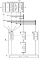
FIG. 2 , the controlpower supply device 100 according to the embodiment of the present invention supplies stable voltages to thecontroller 14 and theauxiliary circuit 15 included in the inverter 10. The controlpower supply device 100 may include adown converter 110, a main SMPS 120, an auxiliary SMPS 130, and anSMPS controller 140. - The
down converter 110 steps down a voltage of the DC-link 12 to output it to themain SMPS 120 and theauxiliary SMPS 130. Thedown converter 110 may be a buck converter. - The
main SMPS 120 and theauxiliary SMPS 130 are supplied with an operating voltage through the DC-link 12. Each of themain SMPS 120 and the auxiliary SMPS 130 includes a switching circuit. For example, each of the main SMPS 120 and theauxiliary SMPS 130 may include a MOSFET as the switching circuit. - The
SMPS controller 140 uses the voltage stepped down by thedown converter 110 as an operating power. - In an initial operation of the inverter 10, the
SMPS controller 140 turns on the MOSFET of themain SMPS 120 and turns off the MOSFET of theauxiliary SMPS 130, such that the main SMPS 120 is operated in a normal operation. - The SMPS controller 140 senses, in real time, a voltage output from the
main SMPS 120 during the operation of themain SMPS 120. - The
SMPS controller 140 monitors the sensed voltage from themain SMPS 120. When the sensed voltage from themain SMPS 120 is in an abnormal range, theSMPS controller 140 turns off the MOSFET of themain SMPS 120 and turns on the MOSFET of theauxiliary SMPS 130, so that theauxiliary SMPS 130 is operated. - At the moment when the auxiliary SMPS 130 is operated, the
SMPS controller 140 stores main SMPS fault history in a memory thereof, and transmits trip information to thecontroller 14 such that trip history is stored, allowing a user to see the trip history. The trip information indicates that an SMPS fault occurred in the main SMPS 120 and accordingly the auxiliary SMPS 130 has been operated. Upon receiving the trip information from theSMPS controller 140, thecontroller 14 may provide the trip information to the user. - When the
auxiliary SMPS 130 is operated, a normal operation of the inverter 10 can be performed using theauxiliary SMPS 130. - The
main SMPS 120 and theauxiliary SMPS 130, according to specifications of the inverter 10, may supply all voltages of 3.3 V, 5 V, 7 V, 15 V, and 24 V, or may selectively supply only a required voltage. For example, thecontroller 14 may be supplied with the voltage of 3.3 V from themain SMPS 120 and theauxiliary SMPS 130. Theauxiliary circuit 15 may be supplied with voltages of 5 V, 7 V, 15 V, and 24 V, which are set to operate an I/O circuit, a communications circuit, a gate drive circuit, and a fan drive circuit, respectively. It will be understood that themain SMPS 120 and theauxiliary SMPS 130 do not necessarily supply voltages of 3.3 V, 5 V, 7 V, 15 V, and 24 V, and may supply voltages having other magnitudes. - The
SMPS controller 140 may perform control power supply in various modes according to specifications of the inverter 10. - For example, the
SMPS controller 140 may perform a first mode in which trip information is transmitted to thecontroller 14 and theauxiliary SMPS 130 supplies a voltage only to thecontroller 14. - For example, the
SMPS controller 140 may perform a second mode in which trip information is transmitted to thecontroller 14 and theauxiliary SMPS 130 supplies, to thecontroller 14 and theauxiliary circuit 15, a minimum power including a gate drive power for restarting the inverter 10 and an I/O power. - For example, the
SMPS controller 140 may perform a third mode in which trip information is transmitted to thecontroller 14 and theauxiliary SMPS 130 supplies, to thecontroller 14 and theauxiliary circuit 15, a maximum power including a power including a gate drive power for restarting the inverter 10 and an I/O voltage, and power for communications and fan control. - For example, a compact inverter has limited space and cost. Therefore, the first mode may be performed such that the
auxiliary SMPS 130 supplies power only to thecontroller 14 and only trip information is transmitted to thecontroller 14, allowing a user to see trip history. - For example, in a standard-grade inverter, the second mode may be performed such that the
auxiliary SMPS 130 supplies, to thecontroller 14 and theauxiliary circuit 15, only the minimum power including power for thecontroller 14, an I/O power, and a gate drive power, allowing a user to see trip history and restart the inverter. - For example, in a premium grade inverter that requires high reliability, the third mode may be performed such that the
auxiliary SMPS 130 supplies all voltages to thecontroller 14 and theauxiliary circuit 15; allowing a user to see trip history, restart the inverter, as well as auxiliary operations including communications and fan driving. -
FIG. 3 is a flowchart illustrating a power supply control method in the control power supply device according to an embodiment of the present invention. - Referring to
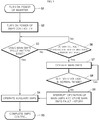
FIG. 3 , upon being powered, the inverter 10 enters the on-state (S1). As the inverter 10 is powered, theSMPS controller 140 is supplied with the power from the DC-link 12 of the inverter 10, to enter the on state (S2). TheSMPS controller 140 searches for the memory therein and determines whether main SMPS fault history is stored in the memory (S3). To this end, theSMPS controller 140 stores the main SMPS fault history in the memory. When the operation of themain SMPS 120 is interrupted and theauxiliary SMPS 130 is operated as a fault occurs in themain SMPS 120, the main SMPS fault history may be created by theSMPS controller 140 to be stored in the memory. The main SMPS fault history stored in the memory may be deleted by theSMPS controller 140 when the operation of themain SMPS 120 is returned to a normal operation through repair or replacement of themain SMPS 120. The determination as to whether the operation of themain SMPS 120 has been returned to the normal operation and the deletion of the main SMPS fault history may be performed by theSMPS controller 140 through a system operator's manipulation. However, the present invention is not limited thereto. Alternatively, theSMPS controller 140 may periodically determine whether the operation of themain SMPS 120 has been returned to the normal operation, and delete the main SMPS fault history from the memory when it is determined that the operation of themain SMPS 120 has been returned to the normal operation. - If it is determined in step S3 that there is a main SMPS fault history, the
SMPS controller 140 determines that a problem has occurred in themain SMPS 120, and turns of the auxiliary SMPS 130 (S4). To this end, theSMPS controller 140 turns on the MOSFET of theauxiliary SMPS 130. Accordingly, SMPS control is completed (S5). - If it is determined in step S3 that there is no main SMPS fault history, the
SMPS controller 140 compares a DC-link voltage with an operating voltage of themain SMPS 120 plus a margin voltage, thereby determining which one is larger. The margin voltage refers to an allowable error in voltage from the normal range, which is smaller or greater than the operating voltage set based on specifications of themain SMPS 120. For example, the margin voltage may be + 10 V. - If it is determined in step S6 that the DC-link voltage is greater than the operating voltage of the
main SMPS 120 plus 10 V, theSMPS controller 140 recognizes that information on an output voltage sensed from themain SMPS 120 is valid information, and allows themain SMPS 120 to be operated (S7). To this end, theSMPS controller 140 turns on the MOSFET of themain SMPS 120. In this regard, a voltage margin for determining the validity of the output voltage sensed from themain SMPS 120 by theSMPS controller 140 is set to 10 V. - The margin of 10 V is considered because power is not yet supplied to the
main SMPS 120 at the moment when the power is supplied to the inverter 10. - Without considering such margin, it may be erroneously determined that there is an SMPS error in the
main SMPS 120 because themain SMPS 120 is not operated and the sensed information frommain SMPS 120 is out of the normal range. - Even when the power of the inverter 10 is turned off, the
SMPS controller 140 compares the DC-link voltage with the operating voltage of themain SMPS 120 plus 10 V, thereby determining that the sensed information of themain SMPS 120 is not valid after the power of themain SMPS 120 is completely turned off, which is safe. - If the operation of the
main SMPS 120 enters the on state, theSMPS controller 140 senses an output voltage from themain SMPS 120, thereby determining whether the sensed voltage is in a preset normal range (S8). - If it is determined that the sensed voltage is within the normal range, the
main SMPS 120 continuously remains in the on state. On the other hand, if it is determined that the sensed voltage is not in the normal range, the operation of theSMPS 120 is interrupted, and a main SMPS fault history is stored in the memory (S9). Then, theauxiliary SMPS 130 is operated (S4), thereby completing the SMPS control (S5). - For standard and premium grade products, reliability is more important than size and price. In the case that an inverter used in a crane, a production line, etc., is interrupted due to the failure that an SMPS is not working, this may result in a great amount of monetary loss and even casualties. Therefore, high reliability is economical in terms of cost.
- According to the present invention, trip information is provided to a user, so that the user can accurately grasp the situation.
- Also, according to the present invention, power required in operations of the auxiliary SMPS is supplied by performing various operating modes, so that the transmission of trip information and the operation of the inverter can be continuously performed. Thus, it is possible to reduce user's risk and to promote user's convenience. Furthermore, it is possible to provide high reliability.
- While the present invention has been described in connection with the preferred embodiments, it will be understood by those skilled in the art that various modifications and changes can be made thereto without departing from the spirit and scope of the invention defined by the appended claims.
Claims (11)
- A control power supply device for an inverter, which supplies stable power to the inverter, the control power supply device comprising:a main switched-mode power supply, SMPS, (120) configured to supply rated voltages to a controller and an auxiliary circuit of the inverter;an auxiliary SMPS (130) configured to be operated when the main SMPS (120) is interrupted to supply the rated voltages to the controller (14) and the auxiliary circuit (15) of the inverter ; andan SMPS controller (140) configured to sense an output voltage from the main SMPS (120), determine whether the sensed voltage is within a normal range and interrupt the main SMPS (120) and operate the auxiliary SMPS (130) if not, and transmit trip information to the controller (14).
- The control power supply device according to claim 1, wherein the SMPS controller (140) stores a main SMPS fault history in a memory when the sensed voltage is not within the normal range.
- The control power supply device according to claim 2, wherein the SMPS controller (140), upon being powered, determines whether there is a main SMPS fault history stored in the memory, interrupts the main SMPS (120) and operates the auxiliary SMPS (130) if so, and transmits the tip information to the controller (14).
- The control power supply device according to one of claim 1 to 3, wherein the SMPS controller (140) senses an output voltage from the main SMPS (120) when a DC-link voltage of the inverter is greater than a set voltage at the time of turning on or off the inverter, and determines whether the sensed voltage is in the normal range.
- The control power supply device according to claim 4, wherein the set voltage level is an operating voltage of the main SMPS (120) plus a margin voltage.
- The control power supply device according to claim 1, further comprising a down converter (110) configured to step down a voltage from a DC-link of the inverter and output it to the SMPS controller (140).
- The control power supply device according to claim 1, wherein the main SMPS (120) and the auxiliary SMPS (130) are supplied with an operating voltage from the DC-link of the inverter.
- The control power supply device according to claim 1, wherein the controller indicates the trip information received from the SMPS controller (140) to a user.
- The control power supply device according to claim 1, wherein a first mode is performed in which the SMPS controller (140) transmits the trip information to the controller and the auxiliary SMPS (140) supplies a voltage only to the controller (14).
- The control power supply device according to claim 1, wherein a second mode is performed in which the SMPS controller (140) transmits the trip information to the controller (14) and the auxiliary SMPS (130) supplies the controller (14) and the auxiliary circuit (15) with a minimum power including a gate drive power for restarting the inverter and an I/O power.
- The control power supply device according to claim 1, wherein a third mode is performed in which the SMPS controller (140) transmits the trip information to the controller (14) and the auxiliary SMPS (130) supplies the controller (14) and the auxiliary circuit (15) with a maximum voltage including a gate drive power for restarting the inverter and an I/O power, and power for communications and fan control.
Applications Claiming Priority (1)
| Application Number | Priority Date | Filing Date | Title |
|---|---|---|---|
| KR1020150077695A KR102024286B1 (en) | 2015-06-02 | 2015-06-02 | Control power supply device for inverter |
Publications (3)
| Publication Number | Publication Date |
|---|---|
| EP3101791A2 true EP3101791A2 (en) | 2016-12-07 |
| EP3101791A3 EP3101791A3 (en) | 2017-04-19 |
| EP3101791B1 EP3101791B1 (en) | 2022-08-31 |
Family
ID=55967163
Family Applications (1)
| Application Number | Title | Priority Date | Filing Date |
|---|---|---|---|
| EP16169363.5A Active EP3101791B1 (en) | 2015-06-02 | 2016-05-12 | Control power supply device for inverter |
Country Status (6)
| Country | Link |
|---|---|
| US (1) | US9876441B2 (en) |
| EP (1) | EP3101791B1 (en) |
| JP (1) | JP6705582B2 (en) |
| KR (1) | KR102024286B1 (en) |
| CN (1) | CN106230271B (en) |
| ES (1) | ES2926901T3 (en) |
Cited By (2)
| Publication number | Priority date | Publication date | Assignee | Title |
|---|---|---|---|---|
| EP3379711A1 (en) * | 2017-03-20 | 2018-09-26 | LSIS Co., Ltd. | Managing device for cooling inverter |
| EP4462661A1 (en) * | 2023-05-10 | 2024-11-13 | Huawei Digital Power Technologies Co., Ltd. | Motor controller and powertrain |
Families Citing this family (4)
| Publication number | Priority date | Publication date | Assignee | Title |
|---|---|---|---|---|
| KR102006730B1 (en) * | 2017-03-23 | 2019-08-02 | 두산중공업 주식회사 | Multiplexing control method and analog output module |
| US10019021B1 (en) | 2017-09-22 | 2018-07-10 | Qualcomm Incorporated | Voltage settling detection for switching regulators |
| FR3153965A1 (en) * | 2023-10-09 | 2025-04-11 | Valeo Eautomotive Germany Gmbh | Electrical system for electric or hybrid vehicle, comprising a voltage converter, an inverter and a control card on the same substrate |
| CN118641865A (en) * | 2024-06-28 | 2024-09-13 | 胜利油田胜兴变压器有限责任公司 | Submersible electric pump transformer performance test system based on multi-terminal analysis |
Family Cites Families (29)
| Publication number | Priority date | Publication date | Assignee | Title |
|---|---|---|---|---|
| JPS5847918U (en) | 1981-09-22 | 1983-03-31 | 日本電気株式会社 | Dual power supply circuit |
| JPS6387193A (en) | 1986-09-29 | 1988-04-18 | Toyo Electric Mfg Co Ltd | D.c. voltage detecting circuit for voltage type inverter |
| US5315533A (en) * | 1991-05-17 | 1994-05-24 | Best Power Technology, Inc. | Back-up uninterruptible power system |
| JP3084800B2 (en) * | 1991-07-24 | 2000-09-04 | 日本電気株式会社 | Power supply method |
| JP2876581B2 (en) * | 1992-12-02 | 1999-03-31 | 三菱電機株式会社 | Power supply |
| JP3309494B2 (en) | 1993-06-08 | 2002-07-29 | 株式会社明電舎 | Inverter power failure countermeasure circuit |
| JP3369346B2 (en) * | 1995-02-21 | 2003-01-20 | ファナック株式会社 | Power outage control device |
| US5602462A (en) * | 1995-02-21 | 1997-02-11 | Best Power Technology, Incorporated | Uninterruptible power system |
| JP2842375B2 (en) | 1996-04-19 | 1999-01-06 | 日本電気株式会社 | Power control device |
| KR100324743B1 (en) * | 1999-01-28 | 2002-02-20 | 구자홍 | Over load sensing method for electrical equipment |
| KR100332799B1 (en) | 2000-01-20 | 2002-04-18 | 구자홍 | Over current protection circuit for inverter |
| JP4311915B2 (en) * | 2002-06-05 | 2009-08-12 | 株式会社リコー | DC-DC converter with voltage detection function |
| US8540493B2 (en) * | 2003-12-08 | 2013-09-24 | Sta-Rite Industries, Llc | Pump control system and method |
| KR200345177Y1 (en) * | 2003-12-10 | 2004-03-16 | 이기석 | Apparatus for Preventing the Inrush Current in the Refrigerator |
| KR100576840B1 (en) * | 2004-03-31 | 2006-05-10 | 주식회사 해성산전 | Elevator emergency operation device |
| US20060259202A1 (en) * | 2005-01-24 | 2006-11-16 | Vaish Himangshu R | Signaling system |
| JP2008067559A (en) * | 2006-09-11 | 2008-03-21 | Sony Corp | Electronics |
| ES2689089T3 (en) * | 2007-02-13 | 2018-11-08 | Otis Elevator Company | Automatic rescue operation for a regenerative drive system |
| US8330381B2 (en) * | 2009-05-14 | 2012-12-11 | Ilumisys, Inc. | Electronic circuit for DC conversion of fluorescent lighting ballast |
| JP5412993B2 (en) * | 2009-06-26 | 2014-02-12 | 富士電機株式会社 | Safety device and power converter |
| KR101062605B1 (en) | 2009-10-30 | 2011-09-06 | 대성전기공업 주식회사 | DC / AC inverter overload protection device and DC / AC inverter including the same |
| JP5220063B2 (en) | 2010-06-24 | 2013-06-26 | ハウス食品株式会社 | A processed wasabi product containing allyl isothiocyanate with a wasabi-like flavor. |
| JP5146514B2 (en) * | 2010-11-09 | 2013-02-20 | 日本電気株式会社 | Switching device, switching device control method, switching device control program |
| BRPI1100270B1 (en) | 2011-02-25 | 2019-03-19 | Embraco Indústria De Compressores E Soluções Em Refrigeração Ltda | ELECTRONIC CONTROL SYSTEM AND METHOD OF A VARIABLE CAPACITY COMPRESSOR |
| KR101354792B1 (en) * | 2012-07-13 | 2014-01-23 | 엘에스산전 주식회사 | Power cabel breaking detection method of inverter system |
| US9401640B2 (en) * | 2013-04-11 | 2016-07-26 | Telefonaktiebolaget L M Ericsson (Publ) | Voltage droop control in a voltage-regulated switched mode power supply |
| KR101452634B1 (en) * | 2013-05-20 | 2014-10-22 | 엘에스산전 주식회사 | Method for detecting power cable state in inverter system |
| KR101768256B1 (en) | 2013-08-29 | 2017-08-14 | 엘에스산전 주식회사 | Inverter with power cell of dual structure |
| DE102013014427A1 (en) * | 2013-08-30 | 2015-03-05 | Liebherr-Elektronik Gmbh | Drive circuit for air bearing motor |
-
2015
- 2015-06-02 KR KR1020150077695A patent/KR102024286B1/en active Active
-
2016
- 2016-05-12 ES ES16169363T patent/ES2926901T3/en active Active
- 2016-05-12 EP EP16169363.5A patent/EP3101791B1/en active Active
- 2016-05-27 CN CN201610366115.1A patent/CN106230271B/en not_active Expired - Fee Related
- 2016-05-31 US US15/169,127 patent/US9876441B2/en active Active
- 2016-06-02 JP JP2016110630A patent/JP6705582B2/en not_active Expired - Fee Related
Non-Patent Citations (1)
| Title |
|---|
| None |
Cited By (3)
| Publication number | Priority date | Publication date | Assignee | Title |
|---|---|---|---|---|
| EP3379711A1 (en) * | 2017-03-20 | 2018-09-26 | LSIS Co., Ltd. | Managing device for cooling inverter |
| US10251320B2 (en) | 2017-03-20 | 2019-04-02 | Lsis Co., Ltd. | Managing device for cooling inverter |
| EP4462661A1 (en) * | 2023-05-10 | 2024-11-13 | Huawei Digital Power Technologies Co., Ltd. | Motor controller and powertrain |
Also Published As
| Publication number | Publication date |
|---|---|
| KR20160141967A (en) | 2016-12-12 |
| EP3101791A3 (en) | 2017-04-19 |
| EP3101791B1 (en) | 2022-08-31 |
| CN106230271A (en) | 2016-12-14 |
| JP2016226283A (en) | 2016-12-28 |
| JP6705582B2 (en) | 2020-06-03 |
| US20160359428A1 (en) | 2016-12-08 |
| KR102024286B1 (en) | 2019-09-23 |
| ES2926901T3 (en) | 2022-10-31 |
| CN106230271B (en) | 2019-05-28 |
| US9876441B2 (en) | 2018-01-23 |
Similar Documents
| Publication | Publication Date | Title |
|---|---|---|
| US9876441B2 (en) | Control power supply device for inverter | |
| US10090795B2 (en) | Motor drive having function of protecting dynamic braking circuit | |
| CN111656666B (en) | power conversion device | |
| US20140070743A1 (en) | Motor drive device with alarm level setting unit | |
| EP2675060A1 (en) | Power conversion apparatus | |
| JP6496371B2 (en) | Motor drive device in which step-up rate of PWM converter is controlled | |
| JP2017017805A (en) | Motor drive device having means for detecting abnormal heat generation of initial charge circuit | |
| JP6133827B2 (en) | Motor driving device having welding detection function of magnetic contactor | |
| US11128252B2 (en) | Motor drive device | |
| KR102526874B1 (en) | Apparatus for controlling operation of power conversion device | |
| EP2017951B1 (en) | Restart control of an A.C. motor drive | |
| JP2011120366A (en) | Overvoltage protection device | |
| US12525782B2 (en) | Motor drive device provided with charging control unit | |
| KR102036115B1 (en) | Air conditioner having function of protecting compressor | |
| JP2013153603A (en) | Motor controller | |
| CN105324934A (en) | Dual power mode drive | |
| US20170302213A1 (en) | Motor drive device suppressing voltage fluctuation in dc link capacitor | |
| KR20210103206A (en) | Apparatus and method for controlling relay of inverter initial charging circuit | |
| JP2020129904A (en) | Switching power supply device and motor drive control system using the same | |
| EP4683205A1 (en) | Soft start control method for multiple motors, and inverter using same | |
| EP4436034A1 (en) | Robot controller and electric discharge method | |
| US11791757B2 (en) | Extended braking with variable frequency drive without input power | |
| JP2013005463A (en) | Power supply circuit | |
| JP2014230334A (en) | Semiconductor electric power conversion system and rapid discharging method for dc intermediate capacitor | |
| CN105656390A (en) | Small power frequency conversion speed regulation driving device |
Legal Events
| Date | Code | Title | Description |
|---|---|---|---|
| PUAI | Public reference made under article 153(3) epc to a published international application that has entered the european phase |
Free format text: ORIGINAL CODE: 0009012 |
|
| STAA | Information on the status of an ep patent application or granted ep patent |
Free format text: STATUS: THE APPLICATION HAS BEEN PUBLISHED |
|
| AK | Designated contracting states |
Kind code of ref document: A2 Designated state(s): AL AT BE BG CH CY CZ DE DK EE ES FI FR GB GR HR HU IE IS IT LI LT LU LV MC MK MT NL NO PL PT RO RS SE SI SK SM TR |
|
| AX | Request for extension of the european patent |
Extension state: BA ME |
|
| PUAL | Search report despatched |
Free format text: ORIGINAL CODE: 0009013 |
|
| AK | Designated contracting states |
Kind code of ref document: A3 Designated state(s): AL AT BE BG CH CY CZ DE DK EE ES FI FR GB GR HR HU IE IS IT LI LT LU LV MC MK MT NL NO PL PT RO RS SE SI SK SM TR |
|
| AX | Request for extension of the european patent |
Extension state: BA ME |
|
| RIC1 | Information provided on ipc code assigned before grant |
Ipc: H02J 9/02 20060101ALI20170313BHEP Ipc: H02J 9/06 20060101ALI20170313BHEP Ipc: H02M 1/00 20070101AFI20170313BHEP |
|
| STAA | Information on the status of an ep patent application or granted ep patent |
Free format text: STATUS: REQUEST FOR EXAMINATION WAS MADE |
|
| 17P | Request for examination filed |
Effective date: 20171016 |
|
| RBV | Designated contracting states (corrected) |
Designated state(s): AL AT BE BG CH CY CZ DE DK EE ES FI FR GB GR HR HU IE IS IT LI LT LU LV MC MK MT NL NO PL PT RO RS SE SI SK SM TR |
|
| STAA | Information on the status of an ep patent application or granted ep patent |
Free format text: STATUS: EXAMINATION IS IN PROGRESS |
|
| 17Q | First examination report despatched |
Effective date: 20210216 |
|
| REG | Reference to a national code |
Ref country code: DE Ref legal event code: R079 Ref document number: 602016074603 Country of ref document: DE Free format text: PREVIOUS MAIN CLASS: H02M0001000000 Ipc: H02M0007480000 |
|
| GRAP | Despatch of communication of intention to grant a patent |
Free format text: ORIGINAL CODE: EPIDOSNIGR1 |
|
| STAA | Information on the status of an ep patent application or granted ep patent |
Free format text: STATUS: GRANT OF PATENT IS INTENDED |
|
| RIC1 | Information provided on ipc code assigned before grant |
Ipc: H02J 9/06 20060101ALI20220317BHEP Ipc: H02M 7/48 20070101AFI20220317BHEP |
|
| INTG | Intention to grant announced |
Effective date: 20220420 |
|
| GRAS | Grant fee paid |
Free format text: ORIGINAL CODE: EPIDOSNIGR3 |
|
| GRAA | (expected) grant |
Free format text: ORIGINAL CODE: 0009210 |
|
| STAA | Information on the status of an ep patent application or granted ep patent |
Free format text: STATUS: THE PATENT HAS BEEN GRANTED |
|
| AK | Designated contracting states |
Kind code of ref document: B1 Designated state(s): AL AT BE BG CH CY CZ DE DK EE ES FI FR GB GR HR HU IE IS IT LI LT LU LV MC MK MT NL NO PL PT RO RS SE SI SK SM TR |
|
| REG | Reference to a national code |
Ref country code: CH Ref legal event code: EP Ref country code: GB Ref legal event code: FG4D |
|
| REG | Reference to a national code |
Ref country code: AT Ref legal event code: REF Ref document number: 1516043 Country of ref document: AT Kind code of ref document: T Effective date: 20220915 |
|
| REG | Reference to a national code |
Ref country code: DE Ref legal event code: R096 Ref document number: 602016074603 Country of ref document: DE |
|
| REG | Reference to a national code |
Ref country code: IE Ref legal event code: FG4D |
|
| REG | Reference to a national code |
Ref country code: ES Ref legal event code: FG2A Ref document number: 2926901 Country of ref document: ES Kind code of ref document: T3 Effective date: 20221031 |
|
| REG | Reference to a national code |
Ref country code: LT Ref legal event code: MG9D |
|
| REG | Reference to a national code |
Ref country code: NL Ref legal event code: MP Effective date: 20220831 |
|
| PG25 | Lapsed in a contracting state [announced via postgrant information from national office to epo] |
Ref country code: SE Free format text: LAPSE BECAUSE OF FAILURE TO SUBMIT A TRANSLATION OF THE DESCRIPTION OR TO PAY THE FEE WITHIN THE PRESCRIBED TIME-LIMIT Effective date: 20220831 Ref country code: RS Free format text: LAPSE BECAUSE OF FAILURE TO SUBMIT A TRANSLATION OF THE DESCRIPTION OR TO PAY THE FEE WITHIN THE PRESCRIBED TIME-LIMIT Effective date: 20220831 Ref country code: NO Free format text: LAPSE BECAUSE OF FAILURE TO SUBMIT A TRANSLATION OF THE DESCRIPTION OR TO PAY THE FEE WITHIN THE PRESCRIBED TIME-LIMIT Effective date: 20221130 Ref country code: LV Free format text: LAPSE BECAUSE OF FAILURE TO SUBMIT A TRANSLATION OF THE DESCRIPTION OR TO PAY THE FEE WITHIN THE PRESCRIBED TIME-LIMIT Effective date: 20220831 Ref country code: LT Free format text: LAPSE BECAUSE OF FAILURE TO SUBMIT A TRANSLATION OF THE DESCRIPTION OR TO PAY THE FEE WITHIN THE PRESCRIBED TIME-LIMIT Effective date: 20220831 Ref country code: FI Free format text: LAPSE BECAUSE OF FAILURE TO SUBMIT A TRANSLATION OF THE DESCRIPTION OR TO PAY THE FEE WITHIN THE PRESCRIBED TIME-LIMIT Effective date: 20220831 |
|
| REG | Reference to a national code |
Ref country code: AT Ref legal event code: MK05 Ref document number: 1516043 Country of ref document: AT Kind code of ref document: T Effective date: 20220831 |
|
| PG25 | Lapsed in a contracting state [announced via postgrant information from national office to epo] |
Ref country code: PL Free format text: LAPSE BECAUSE OF FAILURE TO SUBMIT A TRANSLATION OF THE DESCRIPTION OR TO PAY THE FEE WITHIN THE PRESCRIBED TIME-LIMIT Effective date: 20220831 Ref country code: IS Free format text: LAPSE BECAUSE OF FAILURE TO SUBMIT A TRANSLATION OF THE DESCRIPTION OR TO PAY THE FEE WITHIN THE PRESCRIBED TIME-LIMIT Effective date: 20221231 Ref country code: HR Free format text: LAPSE BECAUSE OF FAILURE TO SUBMIT A TRANSLATION OF THE DESCRIPTION OR TO PAY THE FEE WITHIN THE PRESCRIBED TIME-LIMIT Effective date: 20220831 Ref country code: GR Free format text: LAPSE BECAUSE OF FAILURE TO SUBMIT A TRANSLATION OF THE DESCRIPTION OR TO PAY THE FEE WITHIN THE PRESCRIBED TIME-LIMIT Effective date: 20221201 |
|
| PG25 | Lapsed in a contracting state [announced via postgrant information from national office to epo] |
Ref country code: SM Free format text: LAPSE BECAUSE OF FAILURE TO SUBMIT A TRANSLATION OF THE DESCRIPTION OR TO PAY THE FEE WITHIN THE PRESCRIBED TIME-LIMIT Effective date: 20220831 Ref country code: RO Free format text: LAPSE BECAUSE OF FAILURE TO SUBMIT A TRANSLATION OF THE DESCRIPTION OR TO PAY THE FEE WITHIN THE PRESCRIBED TIME-LIMIT Effective date: 20220831 Ref country code: PT Free format text: LAPSE BECAUSE OF FAILURE TO SUBMIT A TRANSLATION OF THE DESCRIPTION OR TO PAY THE FEE WITHIN THE PRESCRIBED TIME-LIMIT Effective date: 20230102 Ref country code: DK Free format text: LAPSE BECAUSE OF FAILURE TO SUBMIT A TRANSLATION OF THE DESCRIPTION OR TO PAY THE FEE WITHIN THE PRESCRIBED TIME-LIMIT Effective date: 20220831 Ref country code: CZ Free format text: LAPSE BECAUSE OF FAILURE TO SUBMIT A TRANSLATION OF THE DESCRIPTION OR TO PAY THE FEE WITHIN THE PRESCRIBED TIME-LIMIT Effective date: 20220831 Ref country code: AT Free format text: LAPSE BECAUSE OF FAILURE TO SUBMIT A TRANSLATION OF THE DESCRIPTION OR TO PAY THE FEE WITHIN THE PRESCRIBED TIME-LIMIT Effective date: 20220831 |
|
| PG25 | Lapsed in a contracting state [announced via postgrant information from national office to epo] |
Ref country code: SK Free format text: LAPSE BECAUSE OF FAILURE TO SUBMIT A TRANSLATION OF THE DESCRIPTION OR TO PAY THE FEE WITHIN THE PRESCRIBED TIME-LIMIT Effective date: 20220831 Ref country code: EE Free format text: LAPSE BECAUSE OF FAILURE TO SUBMIT A TRANSLATION OF THE DESCRIPTION OR TO PAY THE FEE WITHIN THE PRESCRIBED TIME-LIMIT Effective date: 20220831 |
|
| REG | Reference to a national code |
Ref country code: DE Ref legal event code: R097 Ref document number: 602016074603 Country of ref document: DE |
|
| PG25 | Lapsed in a contracting state [announced via postgrant information from national office to epo] |
Ref country code: NL Free format text: LAPSE BECAUSE OF FAILURE TO SUBMIT A TRANSLATION OF THE DESCRIPTION OR TO PAY THE FEE WITHIN THE PRESCRIBED TIME-LIMIT Effective date: 20220831 Ref country code: AL Free format text: LAPSE BECAUSE OF FAILURE TO SUBMIT A TRANSLATION OF THE DESCRIPTION OR TO PAY THE FEE WITHIN THE PRESCRIBED TIME-LIMIT Effective date: 20220831 |
|
| PLBE | No opposition filed within time limit |
Free format text: ORIGINAL CODE: 0009261 |
|
| STAA | Information on the status of an ep patent application or granted ep patent |
Free format text: STATUS: NO OPPOSITION FILED WITHIN TIME LIMIT |
|
| 26N | No opposition filed |
Effective date: 20230601 |
|
| PG25 | Lapsed in a contracting state [announced via postgrant information from national office to epo] |
Ref country code: SI Free format text: LAPSE BECAUSE OF FAILURE TO SUBMIT A TRANSLATION OF THE DESCRIPTION OR TO PAY THE FEE WITHIN THE PRESCRIBED TIME-LIMIT Effective date: 20220831 |
|
| REG | Reference to a national code |
Ref country code: DE Ref legal event code: R119 Ref document number: 602016074603 Country of ref document: DE |
|
| REG | Reference to a national code |
Ref country code: CH Ref legal event code: PL |
|
| PG25 | Lapsed in a contracting state [announced via postgrant information from national office to epo] |
Ref country code: MC Free format text: LAPSE BECAUSE OF FAILURE TO SUBMIT A TRANSLATION OF THE DESCRIPTION OR TO PAY THE FEE WITHIN THE PRESCRIBED TIME-LIMIT Effective date: 20220831 |
|
| GBPC | Gb: european patent ceased through non-payment of renewal fee |
Effective date: 20230512 |
|
| REG | Reference to a national code |
Ref country code: BE Ref legal event code: MM Effective date: 20230531 |
|
| PG25 | Lapsed in a contracting state [announced via postgrant information from national office to epo] |
Ref country code: MC Free format text: LAPSE BECAUSE OF FAILURE TO SUBMIT A TRANSLATION OF THE DESCRIPTION OR TO PAY THE FEE WITHIN THE PRESCRIBED TIME-LIMIT Effective date: 20220831 Ref country code: LU Free format text: LAPSE BECAUSE OF NON-PAYMENT OF DUE FEES Effective date: 20230512 Ref country code: LI Free format text: LAPSE BECAUSE OF NON-PAYMENT OF DUE FEES Effective date: 20230531 Ref country code: CH Free format text: LAPSE BECAUSE OF NON-PAYMENT OF DUE FEES Effective date: 20230531 |
|
| REG | Reference to a national code |
Ref country code: IE Ref legal event code: MM4A |
|
| PG25 | Lapsed in a contracting state [announced via postgrant information from national office to epo] |
Ref country code: IE Free format text: LAPSE BECAUSE OF NON-PAYMENT OF DUE FEES Effective date: 20230512 |
|
| PG25 | Lapsed in a contracting state [announced via postgrant information from national office to epo] |
Ref country code: IT Free format text: LAPSE BECAUSE OF NON-PAYMENT OF DUE FEES Effective date: 20230512 Ref country code: IE Free format text: LAPSE BECAUSE OF NON-PAYMENT OF DUE FEES Effective date: 20230512 Ref country code: DE Free format text: LAPSE BECAUSE OF NON-PAYMENT OF DUE FEES Effective date: 20231201 Ref country code: GB Free format text: LAPSE BECAUSE OF NON-PAYMENT OF DUE FEES Effective date: 20230512 |
|
| PG25 | Lapsed in a contracting state [announced via postgrant information from national office to epo] |
Ref country code: FR Free format text: LAPSE BECAUSE OF NON-PAYMENT OF DUE FEES Effective date: 20230531 Ref country code: BE Free format text: LAPSE BECAUSE OF NON-PAYMENT OF DUE FEES Effective date: 20230531 |
|
| REG | Reference to a national code |
Ref country code: ES Ref legal event code: FD2A Effective date: 20240628 |
|
| PG25 | Lapsed in a contracting state [announced via postgrant information from national office to epo] |
Ref country code: ES Free format text: LAPSE BECAUSE OF NON-PAYMENT OF DUE FEES Effective date: 20230513 |
|
| PG25 | Lapsed in a contracting state [announced via postgrant information from national office to epo] |
Ref country code: ES Free format text: LAPSE BECAUSE OF NON-PAYMENT OF DUE FEES Effective date: 20230513 |
|
| PG25 | Lapsed in a contracting state [announced via postgrant information from national office to epo] |
Ref country code: BG Free format text: LAPSE BECAUSE OF FAILURE TO SUBMIT A TRANSLATION OF THE DESCRIPTION OR TO PAY THE FEE WITHIN THE PRESCRIBED TIME-LIMIT Effective date: 20220831 |
|
| PG25 | Lapsed in a contracting state [announced via postgrant information from national office to epo] |
Ref country code: BG Free format text: LAPSE BECAUSE OF FAILURE TO SUBMIT A TRANSLATION OF THE DESCRIPTION OR TO PAY THE FEE WITHIN THE PRESCRIBED TIME-LIMIT Effective date: 20220831 |
|
| PG25 | Lapsed in a contracting state [announced via postgrant information from national office to epo] |
Ref country code: CY Free format text: LAPSE BECAUSE OF FAILURE TO SUBMIT A TRANSLATION OF THE DESCRIPTION OR TO PAY THE FEE WITHIN THE PRESCRIBED TIME-LIMIT; INVALID AB INITIO Effective date: 20160512 |
|
| PG25 | Lapsed in a contracting state [announced via postgrant information from national office to epo] |
Ref country code: HU Free format text: LAPSE BECAUSE OF FAILURE TO SUBMIT A TRANSLATION OF THE DESCRIPTION OR TO PAY THE FEE WITHIN THE PRESCRIBED TIME-LIMIT; INVALID AB INITIO Effective date: 20160512 |
|
| PG25 | Lapsed in a contracting state [announced via postgrant information from national office to epo] |
Ref country code: TR Free format text: LAPSE BECAUSE OF FAILURE TO SUBMIT A TRANSLATION OF THE DESCRIPTION OR TO PAY THE FEE WITHIN THE PRESCRIBED TIME-LIMIT Effective date: 20220831 |