EP3100468B1 - Leistungs- und datenübertragung bei hörprothesen - Google Patents
Leistungs- und datenübertragung bei hörprothesen Download PDFInfo
- Publication number
- EP3100468B1 EP3100468B1 EP15743022.4A EP15743022A EP3100468B1 EP 3100468 B1 EP3100468 B1 EP 3100468B1 EP 15743022 A EP15743022 A EP 15743022A EP 3100468 B1 EP3100468 B1 EP 3100468B1
- Authority
- EP
- European Patent Office
- Prior art keywords
- external
- during
- power
- data
- implantable
- Prior art date
- Legal status (The legal status is an assumption and is not a legal conclusion. Google has not performed a legal analysis and makes no representation as to the accuracy of the status listed.)
- Active
Links
Images


Classifications
-
- A—HUMAN NECESSITIES
- A61—MEDICAL OR VETERINARY SCIENCE; HYGIENE
- A61N—ELECTROTHERAPY; MAGNETOTHERAPY; RADIATION THERAPY; ULTRASOUND THERAPY
- A61N1/00—Electrotherapy; Circuits therefor
- A61N1/18—Applying electric currents by contact electrodes
- A61N1/32—Applying electric currents by contact electrodes alternating or intermittent currents
- A61N1/36—Applying electric currents by contact electrodes alternating or intermittent currents for stimulation
- A61N1/372—Arrangements in connection with the implantation of stimulators
- A61N1/378—Electrical supply
- A61N1/3787—Electrical supply from an external energy source
-
- A—HUMAN NECESSITIES
- A61—MEDICAL OR VETERINARY SCIENCE; HYGIENE
- A61N—ELECTROTHERAPY; MAGNETOTHERAPY; RADIATION THERAPY; ULTRASOUND THERAPY
- A61N1/00—Electrotherapy; Circuits therefor
- A61N1/18—Applying electric currents by contact electrodes
- A61N1/32—Applying electric currents by contact electrodes alternating or intermittent currents
- A61N1/36—Applying electric currents by contact electrodes alternating or intermittent currents for stimulation
- A61N1/36036—Applying electric currents by contact electrodes alternating or intermittent currents for stimulation of the outer, middle or inner ear
- A61N1/36038—Cochlear stimulation
-
- A—HUMAN NECESSITIES
- A61—MEDICAL OR VETERINARY SCIENCE; HYGIENE
- A61N—ELECTROTHERAPY; MAGNETOTHERAPY; RADIATION THERAPY; ULTRASOUND THERAPY
- A61N1/00—Electrotherapy; Circuits therefor
- A61N1/18—Applying electric currents by contact electrodes
- A61N1/32—Applying electric currents by contact electrodes alternating or intermittent currents
- A61N1/36—Applying electric currents by contact electrodes alternating or intermittent currents for stimulation
- A61N1/372—Arrangements in connection with the implantation of stimulators
- A61N1/37211—Means for communicating with stimulators
- A61N1/37217—Means for communicating with stimulators characterised by the communication link, e.g. acoustic or tactile
- A61N1/37223—Circuits for electromagnetic coupling
-
- A—HUMAN NECESSITIES
- A61—MEDICAL OR VETERINARY SCIENCE; HYGIENE
- A61N—ELECTROTHERAPY; MAGNETOTHERAPY; RADIATION THERAPY; ULTRASOUND THERAPY
- A61N1/00—Electrotherapy; Circuits therefor
- A61N1/18—Applying electric currents by contact electrodes
- A61N1/32—Applying electric currents by contact electrodes alternating or intermittent currents
- A61N1/36—Applying electric currents by contact electrodes alternating or intermittent currents for stimulation
- A61N1/372—Arrangements in connection with the implantation of stimulators
- A61N1/37211—Means for communicating with stimulators
- A61N1/37252—Details of algorithms or data aspects of communication system, e.g. handshaking, transmitting specific data or segmenting data
-
- H—ELECTRICITY
- H02—GENERATION; CONVERSION OR DISTRIBUTION OF ELECTRIC POWER
- H02J—ELECTRIC POWER NETWORKS; CIRCUIT ARRANGEMENTS OR SYSTEMS FOR SUPPLYING OR DISTRIBUTING ELECTRIC POWER; SYSTEMS FOR STORING ELECTRIC ENERGY
- H02J50/00—Circuit arrangements or systems for wireless supply or distribution of electric power
- H02J50/10—Circuit arrangements or systems for wireless supply or distribution of electric power using inductive coupling
- H02J50/12—Circuit arrangements or systems for wireless supply or distribution of electric power using inductive coupling of the resonant type
-
- H—ELECTRICITY
- H02—GENERATION; CONVERSION OR DISTRIBUTION OF ELECTRIC POWER
- H02J—ELECTRIC POWER NETWORKS; CIRCUIT ARRANGEMENTS OR SYSTEMS FOR SUPPLYING OR DISTRIBUTING ELECTRIC POWER; SYSTEMS FOR STORING ELECTRIC ENERGY
- H02J50/00—Circuit arrangements or systems for wireless supply or distribution of electric power
- H02J50/80—Circuit arrangements or systems for wireless supply or distribution of electric power involving the exchange of data, concerning supply or distribution of electric power, between transmitting devices and receiving devices
-
- H—ELECTRICITY
- H02—GENERATION; CONVERSION OR DISTRIBUTION OF ELECTRIC POWER
- H02J—ELECTRIC POWER NETWORKS; CIRCUIT ARRANGEMENTS OR SYSTEMS FOR SUPPLYING OR DISTRIBUTING ELECTRIC POWER; SYSTEMS FOR STORING ELECTRIC ENERGY
- H02J50/00—Circuit arrangements or systems for wireless supply or distribution of electric power
- H02J50/90—Circuit arrangements or systems for wireless supply or distribution of electric power involving detection or optimisation of position, e.g. alignment
-
- H—ELECTRICITY
- H02—GENERATION; CONVERSION OR DISTRIBUTION OF ELECTRIC POWER
- H02J—ELECTRIC POWER NETWORKS; CIRCUIT ARRANGEMENTS OR SYSTEMS FOR SUPPLYING OR DISTRIBUTING ELECTRIC POWER; SYSTEMS FOR STORING ELECTRIC ENERGY
- H02J7/00—Circuit arrangements for charging or discharging batteries or for supplying loads from batteries
- H02J7/40—Circuit arrangements for charging or discharging batteries or for supplying loads from batteries characterised by the exchange of charge or discharge related data
- H02J7/42—Circuit arrangements for charging or discharging batteries or for supplying loads from batteries characterised by the exchange of charge or discharge related data with electronic devices having internal batteries, e.g. mobile phones
-
- H—ELECTRICITY
- H04—ELECTRIC COMMUNICATION TECHNIQUE
- H04B—TRANSMISSION
- H04B5/00—Near-field transmission systems, e.g. inductive or capacitive transmission systems
- H04B5/70—Near-field transmission systems, e.g. inductive or capacitive transmission systems specially adapted for specific purposes
- H04B5/79—Near-field transmission systems, e.g. inductive or capacitive transmission systems specially adapted for specific purposes for data transfer in combination with power transfer
-
- H—ELECTRICITY
- H02—GENERATION; CONVERSION OR DISTRIBUTION OF ELECTRIC POWER
- H02J—ELECTRIC POWER NETWORKS; CIRCUIT ARRANGEMENTS OR SYSTEMS FOR SUPPLYING OR DISTRIBUTING ELECTRIC POWER; SYSTEMS FOR STORING ELECTRIC ENERGY
- H02J2105/00—Networks for supplying or distributing electric power characterised by their spatial reach or by the load
- H02J2105/40—Networks for supplying or distributing electric power characterised by their spatial reach or by the load characterised by the loads connecting to the networks or being supplied by the networks
- H02J2105/46—Medical devices, medical implants or life supporting devices
-
- H—ELECTRICITY
- H04—ELECTRIC COMMUNICATION TECHNIQUE
- H04R—LOUDSPEAKERS, MICROPHONES, GRAMOPHONE PICK-UPS OR LIKE ACOUSTIC ELECTROMECHANICAL TRANSDUCERS; ELECTRIC HEARING AIDS; PUBLIC ADDRESS SYSTEMS
- H04R2225/00—Details of deaf aids covered by H04R25/00, not provided for in any of its subgroups
- H04R2225/67—Implantable hearing aids or parts thereof not covered by H04R25/606
Definitions
- the present invention relates generally to hearing prostheses, and more particularly, to power and data transfer in hearing prostheses.
- Implantable medical devices Medical devices having one or more implantable components, generally referred to herein as implantable medical devices, have provided a wide range of therapeutic benefits to recipients over recent decades.
- partially or fully-implantable medical devices such as hearing prostheses (e.g., bone conduction devices, mechanical stimulators, cochlear implants, etc.), implantable pacemakers, defibrillators, functional electrical stimulation devices, and other implantable medical devices, have been successful in performing life saving and/or lifestyle enhancement functions for a number of years.
- implantable medical devices and the ranges of functions performed thereby have increased over the years.
- many implantable medical devices now often include one or more instruments, apparatus, sensors, processors, controllers or other functional mechanical or electrical components that are permanently or temporarily implanted in a recipient.
- These functional components perform diagnosis, prevention, monitoring, treatment or management of a disease or injury or symptom thereof, or to investigate, replace or modify of the anatomy or of a physiological process.
- Many of these functional components utilize power and/or data received from external components that are part of, or operate in conjunction with, the implantable medical device.
- US 2013/0214731 A1 relates to a self-tuning external device for wirelesslv recharging implantable medical devices and discloses all of the features in the preamble of claim 1.
- Implantable medical devices having implantable and external resonant circuits configured to transcutaneously transfer power and data to an implanted coil are described in the state-of-the-art, for example, in the United States patent applications US 2009/0216296 A1 , US 2011/0287717 A1 . US 2002/0032471 A1 , US 2013/0123881 A1 and US 2010/0204756 A1 . US 2011/0287717 A1 addresses the problem of voltage overshoot protection by means of an output signal damping element in the transmission circuitry that is selectively operable according to the value of the data signal.
- US 2002/0032471 A1 addresses the problem that the integrity of the data transmission is significantly adversely affected in proportion to the sharpness of the rise and fall times of the modulated data signal. This problem is solved by providing a modulation amplifier in the external transmitter that selectively alters the Q of the resonant circuit as a function of whether the carrier signal is being modulated with data or not.
- US 2013/0123881 A1 and US 2010/0204756 A1 use different frequencies for power transmission and data transmission.
- the external resonant circuitry of these documents includes a capacitor as a tuning means so that the resonance circuitry is operated in resonance during power transmission and data transmission.
- the present invention provides an implantable medical device as set forth in claim 1. Preferred embodiments are defined in the dependent claims.
- an implantable medical device comprises an implantable resonant circuit comprising an implantable coil, and an external resonant circuit comprising an external coil configured to transcutaneously transfer power and data to the implantable coil using separate power and data time slots. At least one of the external or implantable resonant circuit is substantially more damped during the data time slots than during the power time slots.
- an external transmitter circuit comprises an external resonant circuit comprising an external coil and one or more driver bridges configured to cause the external coil to transfer power and data to an implantable receiver circuit using separate power and data time slots.
- the quality factor of the external resonant circuit is lower during the data slots than during the power time slots.
- an apparatus comprising an implantable resonant circuit comprising an implantable coil, an external resonantcircuit comprising an external coil forming a transcutaneous power and data link with the implantable coil, and at least one driver bridge configured to drive the external coil so as to separately transfer power and data to the implantable coil. Operational characteristics of at least one of the implantable resonant circuit or the external resonant circuit are dynamically adjusted during transfer of data to the implantable coil.
- a method for transmitting power from an external transmitter circuit to an implantable receiver circuit comprises an external resonant circuit that includes an external coil, while the implantable receiver circuit comprise an implantable resonant circuit that includes an implantable coil.
- the method comprises driving the external resonant circuit with one or more driver bridges during a power time slot to cause the external coil to transfer power to the implantable receiver circuit.
- the method further comprises driving the external resonant circuit with one or more driver bridges during a data time slot to cause the external coil to transfer data to the implantable receiver circuit.
- the power and data time slots are different time slots and the external resonant circuit is driven such that the quality factor of the external resonant circuit is lower during the data slot than during the power time slot.
- Embodiments presented herein are generally directed to techniques for separately transferring power and data from an external device to an implantable component of a partially or fully implantable medical device.
- the separated power and data transfer techniques use a single external coil and a single implantable coil.
- the external coil is part of an external resonant circuit, while the implantable coil is part of an implantable resonant circuit.
- the external coil is configured to transcutaneously transfer power and data to the implantable coil using separate (different) power and data time slots.
- At least one of the external or internal resonant circuit is substantially more damped during the data time slot than during the power time slot.
- the external and internal resonant circuits are resonsant tank circuits.
- Embodiments of the present disclosure are described herein primarily in connection with one type of implantable medical devices, namely partially implantable hearing prostheses comprising an external component and an internal (implantable component).
- Hearing prostheses include, but are not limited to, auditory brain stimulators, cochlear implants (also commonly referred to as cochlear implant devices, cochlear prostheses, and the like; simply “cochlear implants” herein), bone conduction devices, and mechanical stimulators. It is to be appreciated that embodiments of the present disclosure may be implemented in any partially or fully implantable medical device now known or later developed.
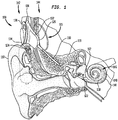
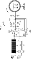
- FIG. 1 is a perspective view of an exemplary cochlear implant 100 configured to implement separated power and data transfer techniques in accordance with embodiments presented herein.
- the cochlear implant 100 includes an external component 142 and an internal or implantable component 144.
- the external component 142 is directly or indirectly attached to the body of the recipient and typically comprises one or more sound input elements 124 (e.g., microphones, telecoils, etc .) for detecting sound, a sound processor 134, a power source (not shown), an external coil 130 and, generally, a magnet (not shown) fixed relative to the external coil 130.
- the sound processor 134 processes electrical signals generated by a sound input element 124 that is positioned, in the depicted embodiment, by auricle 110 of the recipient.
- the sound processor 134 provides the processed signals to a transmitter circuit configured to drive (activate) external coil 130.
- an “external component” refers to one or more elements or devices that are part of, or operate in conjunction with, the implantable medical device.
- an external component may form part of the implantable medical device or may be a separate device that operates with an implantable medical device.
- the implantable component 144 comprises an implant body 105, a lead region 108, and an elongate stimulating assembly 118.
- the implant body 105 comprises a stimulator unit 120, an implantable (internal) coil 136, and an internal receiver/transceiver unit 132, sometimes referred to herein as transceiver unit 132.
- the transceiver unit 132 is connected to the internal coil 136 and, generally, a magnet (not shown) fixed relative to the internal coil 136.
- Internal transceiver unit 132 and stimulator unit 120 are sometimes collectively referred to herein as a stimulator/transceiver unit 120.
- Implantable coil 136 is typically a wire antenna coil comprised of multiple turns of electrically insulated single-strand or multi-strand platinum or gold wire. The electrical insulation of implantable coil 136 is provided by a flexible silicone molding. In use, transceiver unit 132 may be positioned in a recess of the temporal bone of the recipient.
- the magnets in the external component 142 and implantable component 144 facilitate the operational alignment of the external coil 130 with the implantable coil 136.
- the operational alignment of the coils enables the external coil 130 to transmit/receive power and data to the implantable coil 136.
- the external component 142 is configured to transmit electrical signals (i.e., power and data) from external coil 130 to implantable coil 136 using separate time slots over a radio frequency (RF) link.
- RF radio frequency
- Elongate stimulating assembly 118 is implanted in cochlea 140 and includes a contact array 146 comprising a plurality of stimulating contacts 148.
- Stimulating assembly 118 extends through cochleostomy 122 and has a proximal end connected to stimulator unit 120 via lead region 108 that extends through mastoid bone 119.
- Lead region 108 couples the stimulating assembly 118 to implant body 105 and, more particularly, stimulator/transceiver unit 120.
- the stimulating contacts 148 may be electrical contacts, optical contacts, or a combination of optical and electrical contacts.
- a transcutaneous RF link is provided to transfer power and data from external component 142 to implantable component 144.
- Certain conventional transcutaneous RF links use an amplitude modulated signal where the data and the power are transferred simultaneously (i.e., at the same time) over the same RF coil for extraction by the implantable component.
- the data signals are embedded in the power signals for simultaneous transmission from the external coil to the implantable coil.
- RF links that simultaneously transmit power and data are sometimes referred to as combined power and data links.
- first RF link is created between a first external coil and an implantable coil. This first RF link is used solely for data transmission.
- second RF link is created between a second (different) external coil and the implantable coil. This second RF link is used solely for power transmission.
- a time multiplexing scheme is implemented such that either the first RF link or the second RF link is activated and at one time in order to avoid interference between the power and data signals.
- these arrangements use a first RF link (and first external coil) that is dedicated to data transmission and a second RF link (and second external coil) that is dedicated to power transmission where the first and second links are alternatively activated.
- a single transcutaneous RF link is used to separately transfer power and data from an external component to an implantable component.
- transfer of power and data occur during separate (different) time slots using the same external coil 130 (i.e., a shared external coil for both data and power).
- a single transmission sequence/frame may be split into a power time slot (block) and a data time slot (block) and repeated. All of the power towards the implantable component 144 is transferred during the power time slot.
- the operational characteristics of one or both of an external transmitter (or transceiver) or an implantable receiver (or transceiver) are dynamically adjusted between the power and data slots.
- the implantable receiver includes an implantable resonant circuit (e.g., an implantable resonant tank circuit) comprising an implantable coil
- the external transmitter includes an external resonant circuit (e.g., an external resonant tank circuit) comprising an external coil configured to transcutaneously transfer power and data to the implantable coil using the separate power and data time slots.
- At least one of the external or internal resonant circuit is substantially more damped during the data time slot than during the power time slot. That is, the quality factor (Q) of one or both of the external circuit or the internal resonant circuit is reduced during data transmission (relative to the quality factor of one or both of the external circuit or the internal resonant circuit during power transmission).
- embodiments will be primarily described herein with reference to the use of external and implantable resonsant tank circuits. It is to be appreciated that embodiments may include other types of external and/or implantable resonant circuits.
- the techniques presented herein involve switching between power transfer for some fraction of the frame, and then data transfer for another part of the frame.
- the RF link can be optimized for efficient power transfer during the power time slots and then independently optimized for data transfer. For example, a very high quality factor may be used to optimize the power transfer efficiency during the power time slots.
- the internal or external tank circuit is dampened (and optionally detuned) to improve data integrity.
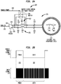
- FIG. 2A is a schematic diagram illustrating a transmitter circuit 220 configured to separately transfer power and data signals from an external component of an implantable component via a single external coil 222.
- the external coil 222 is part of an external resonant tank circuit 225 that also comprises capacitor 242 (capacitor C1) and capacitor 244 (capacitor C2).
- external coil 222 has an inductive component (L HPC ) 246 and some small copper losses represented as the series resistive component (R HPC ) 248.
- the transmitter circuit 220 comprises a driver bridge 240.
- the driver bridge 240 is a full H-bridge driver. In other embodiments, the driver bridge 240 is a half H-bridge driver.
- the driver bridge 240 includes an input 250 that receives an input signal 231 ( FIG. 2B ) via a data input line 252.
- the driver bridge 240 also comprises a first output 254 and a second output 256 (differential output).
- the first output 254 is connected to capacitor 242 (which is connected to external coil 222) via a series circuit 257.
- the series circuit 257 comprises a resistor 258 (R1) in series with an inductor 260 (L1).
- the second output 256 is connected to capacitor 244 (which is also connected to external coil 222) via a series circuit 261.
- the series circuit 261 comprises resistor 262 (R2) in series with an inductor 264 (L2).
- the driver may only contain a single output (Half H-bridge or single push-pull) connected to a single series circuit comprising a resistor (R1) in series with an inductor 260 (L1).
- the first output 254 and the second output 256 of driver bridge 240 are also connected to the capacitors 242 and 244, respectively, via a switch 266.
- the switch 266 When the switch 266 is closed, the first output 254 is directly connected to capacitor 242 so as to bypass series circuit 257 (i.e., bypass resistor 258 and inductor 260).
- the second output 256 is directly connected to capacitor 244 so as to bypass series circuit 261 (i.e., bypass resistor 262 and inductor 264).
- the switch 266 may be closed in response to an enable power signal 233 ( FIG. 2B ) received via enable power line 268.
- FIG. 2B illustrates a power time slot 235 and a data time slot 237 where On-Off keying (OOK) is used to transmit both the power and the data.
- OOK On-Off keying
- the signal may be either a "1" (i.e., a pulse of energy is present) or a "0" (i.e., no pulse of energy is present).
- five (5) cycles or pulses may represent a '1' cell and the absence of energy during five (5) cycles may represent a '0' cell. Energy is taken from the ' 1' cells. As shown in FIG.
- the input signal 231 is all '1s,' but switches between '1s' and '0s' during the data time slot 237.
- the switching between 1s' and '0s' during the data time slot 237 is a digital code that is decoded at the implantable component.
- the enable power signal 233 is a pulse waveform that also alternatives between a value of '1' and '0'. During the power time slot 235, the enable power signal 233 has a value of '1' so as to close the switch 266. This causes the outputs 254 and 256 of the driver bridge 240 to be directly connected to the capacitors 242 and 244, respectively, so as to bypass the series circuits 257 (R1 and L1) and 261 (R2 and L2).
- the resonance frequency of the external resonant tank circuit 225 during the power time slot ( f res_power_timeslot ) is defined below in Equation 1.
- f res _ power _ timeslot 1 2 ⁇ ⁇ L HPC . C 1 . C 2 C 1 + C 2
- the quality factor (Q) of the resonant tank circuit 225 during the power time slot (Q ext_power_timeslot ) is defined below in Equation 2.
- the external coil current is maximized when the resonant frequency of the resonant tank circuit 225 during the power time slot is substantially equal or close to the operating frequency ( f 0 ) of the external coil 222 (i.e., drive more current through the external coil while maintaining the driver at the same voltage). Therefore, the frequency of the external resonant tank circuit 225 is set (via tuning of capacitors 242 and 244) to be close or equal to the operating frequency to maximize the power efficiency of the transcutaneous link.
- the switch 266 is opened so that the series circuits 257 (R1 and L1) and 261 (R2 and L2) are placed in series between the driver bridge 240 and the external coil 222. Placing the series circuits 257 and 261 between the driver bridge 240 and the external coil 222 causes a drop in the quality factor of the resonant tank circuit 225, the external coil current, and the resonance frequency.
- the resonance frequency of the external resonant tank circuit 225 during the data time slot ( f res_data_timeslot ) is defined below in Equation 4.
- f res _ data _ timeslot 1 2 ⁇ ⁇ L HPC + L 1 + L 2 . C 1 . C 2 C 1 + C 2
- the quality factor of the resonant tank circuit 225 during the data time slot (Q ext_data_timeslot ) is defined below in Equation 5.
- the data integrity improves when the external resonant tank circuit 225 is more dampened (i.e., has a lower quality factor) during data transmission. This is opposed to power transmission where, as noted above, maximum power efficiency is achieved when the quality factor of the resonant tank circuit is maximized. As such, in accordance with the techniques presented herein, the quality factor of the resonant tank circuit is maximized during power transmission, but is purposely lowered during data transmission (i.e., Q ext_data_timeslot ⁇ Q ext_power_timeslot ).
- the dampened external resonant tank circuit 225 reduces the ringing effects during one or more '0' cycle transitions after a sequence of ' 1' cycles during use of OOK modulation at f 0 .
- the series resistors 258 and 262 operate to dampen the external resonant tank circuit 225 when connected in series between the between the driver bridge 240 and the external coil 222.
- the data integrity improves and that the external coil current drops during the data time slot when the external resonant tank circuit 225 is tuned lower than the operating frequency.
- the lower the tuning frequency of the external coil 222 is relative to the operating frequency the higher the decrease in current flow through the external coil 222 when the driver bridge 222 is acting as a pulsating voltage source (e.g. Class-D driver bridge).
- the decrease in the external coil current prevents interference of the implantable component load with the data recovery at the implantable component.
- the operating frequency of the external coil 222 is 5 megahertz (MHz) and the resonant frequency of the external resonant tank circuit 225 during data transmission ( f res_data_timeslot ) is set equal to 4.75 MHz).
- the series inductors 260 and 264 operate to reduce the resonant frequency of the external resonant tank circuit 225 when connected in series between the between the driver bridge 240 and the external coil 222.
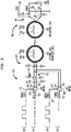
- FIG. 3 illustrates an alternative arrangement where a dedicated driver bridge, rather than a switch, is used to dynamically adjust the resonance frequency and quality factor of an external tank circuit.
- FIG. 3 is a schematic diagram illustrating an external transmitter circuit 320 configured to separately transfer power and data signals to an implantable component via a single external coil 322.
- the external transmitter circuit 320 comprises a first driver bridge 340 (data driver bridge) and a second driver bridge 341 (power driver bridge).
- the driver bridge 340 is enabled during the data time slot, but is deactivated during the power time slot.
- the driver bridge 341 is enabled during the power time slot, but is deactivated during the data time slot.
- the arrangement of FIG. 3 uses dedicated driver bridges for each of data and power transmission (i.e., the data and power signals have their own driver bridges and only a single driver bridge is enabled at a time).
- the external coil 322 is part of an external resonant tank circuit 325 that also comprises capacitor 342 (capacitor C1) and capacitor 344 (capacitor C2).
- external coil 322 has an inductive component (L HPC ) 346 and some small copper losses represented as the series resistive component (R HPC ) 348.
- the driver bridge 340 includes an input 350 that receives an input signal 331 via data input line 352 and an enable data input 353 that receives a enable data signal 329 via enable data signal line 355.
- the driver bridge 340 also comprises a first output 354 and a second output 356.
- the first output 354 is connected to capacitor 342 (which is connected to external coil 322) via a series circuit 357 that comprises a resistor 358 (R1) in series with an inductor 360 (L1).
- the second output 356 is connected to capacitor 344 (which is also connected to external coil 322) via a series circuit 361 that comprises resistor 362 (R2) in series with an inductor 364 (L2).
- the driver bridge 341 includes an input 369 that receives a power signal 327 via power input line 372 and an enable power input 373 configured to receive an enable power signal 327 via enable power signal line 375.
- the driver bridge 341 also comprises a first output 374 and a second output 376.
- the first output 374 is directly connected to capacitor 342 (which is connected to external coil 322) so as to bypass series circuit 357.
- the second output 376 is directly connected to capacitor 344 so as to bypass series circuit 361.
- the power signal 327 is a series of all '1' values (consecutive power cycles), while the data input signal 331 switches between '1s' and '0s' (i.e., at 5 MHz a '1' represents five (5) cycles or pulses during 1 ⁇ 3 and a '0' represents a silence during 1 ⁇ s for a data rate of 1Mbps).
- the enable power signal 333 is a logic signal that alternatives between a value of '1' and '0'.
- the enable data signal 329 is also a pulse waveform that alternatives between a value of '1' and '0'. The enable signal activates the respective driver at value '1'.
- the enable data signal 329 is the inverse of the enable power signal 333(note WME: make this more visible in Fig.3 ). That is, when the enable power signal 333 is '1,' the enable data signal 329 is a '0' value, and vice versa.
- power and data are transmitted during non-overlapping and separate (i.e., different) time slots using the separate driver bridges.
- the enable data signal 329 is high so as to enable driver bridge 340.
- the outputs 354 and 356, generated using data input signal 331 are used to drive external coil 322.
- the enable power signal 333 is low so as to cause the outputs 374 and 376 of driver bridge 341 to be placed in a high impedance state.
- the first output 354 is connected to external coil 322 via series circuit 357 (R1 and L1) and the second output 356 is connected to external coil 322 via series circuit 361 (R2 and L2).
- driver bridge 340 when driver bridge 340 is enabled, the external coil 322 is driven with signals that pass through series circuit 357 and series circuit 361.
- the enable power signal 333 is high (i.e., a '1' value) so as to enable driver bridge 341.
- the outputs 374 and 376 generated using power signal 327, are used to drive external coil 322.
- the enable data signal 329 is low (i.e., a '0' value) so as to cause the outputs 354 and 356 of driver bridge 340 to be placed in a high impedance state.
- the bridge 341 is enabled to drive the external coil 322 with signals that pass directly from the outputs 374 and 376 to capacitors 342 and 344, respectively.
- the signals bypass the series circuits 357 (R1 and L1) and 361 (R2 and L2), thereby ensuring that the quality factor and resonant frequency of the external resonant tank circuit 325 are not affected by the series circuits 357 and 361.
- the data integrity improves when the external resonant tank circuit 325 is more dampened (i.e., has a lower quality factor) during data transmission.
- the driver bridge 340 is enabled so as to drive external coil 322 with signals that pass through the series circuit 357 (R1 and L1) and series circuit 361 (R2 and L2). That is, the series circuit 357 (R1 and L1) and series circuit 361 (R2 and L2) are placed in between the driver bridge 340 and the external coil 322.
- Driving the external coil 322 via the series circuits 357 and 361 causes a drop in the quality factor of the resonant tank circuit 325, the external coil current, and the resonance frequency of the resonant tank circuit.
- R1 and R2 may be an intrinsic part of the data driver bridge.
- the quality factor of the resonant tank circuit 325 is maximized during power transmission, but is purposely lowered during data transmission (i.e., Q ext_data_timeslot ⁇ Q ext_power_timeslot ).
- the dampened external resonant tank circuit 325 reduces the ringing effects during one or more '0' cycle transitions after a sequence of '1' cycles during use of OOK modulation at f 0 .
- the series resistors 358 and 362 operate to dampen the external resonant tank circuit 325 when connected in series between the between the driver bridge 340 and the external coil 322.
- FIG. 3 also illustrates an implantable receiver circuit 380 configured to receive separate power and data signals transmitted by the external transmitter circuit 320.
- the implantable receiver circuit 380 comprises an implantable coil 382 that is part of an implantable (internal) resonant tank circuit 385 that also comprises capacitor 394 (capacitor C4) and capacitor 396 (capacitor C5).
- implantable coil 382 has an inductive component (LI PC ) 377 and some small copper losses represented as the series resistive component (RI PC ) 379.
- the implantable receiver circuit 380 also comprises a data output 381, a load 383 (i.e., battery or other energy storage device), and an energy rectifier connected between the implantable coil 382 and the load 383.
- the energy rectifier 384 is a diode.
- the implantable receiver circuit 380 is described in relation to external transmitter circuit 320. It is to be appreciated that the implantable receiver circuit 380, or variants thereof, may be used with the other external transmitter circuits described herein.
- the data integrity improves and that the current through external coil 322 drops when the external resonant tank circuit 325 is tuned lower than the operating frequency.
- the operating frequency of the external coil 322 is 5 MHz and the resonant frequency of the external resonant tank circuit 325 during data transmission ( f res _ data_timeslot ) is set equal to 4.75 MHz).
- the series inductors 360 and 364 operate to reduce the resonant frequency of the external resonant tank circuit 325 when connected in series between the between the driver bridge 340 and the external coil 322.
- the decrease in the external coil current in response to the detuning of the resonant frequency prevents interference of the implantable component load 383 with the data recovery at the implantable receiver circuit 380. More specifically, the detuning lowers the peak amplitude of the data signals so that the diode 384 is maintained in reverse polarization (i.e., non-conducting during data transmission), thereby preventing the load 383 from being seen at the data output 381.
- the driver bridge 341 is constructed as a full H-bridge driver, while the driver bridge 340 is a half H-bridge driver.
- the use of a half H-bridge driver lowers the peak amplitude of the data signal, thereby assisting in maintaining the diode 384 in reverse polarization.
- Fine adjustments to the received implant voltage level may also be accomplished by altering the pulse width of each RF cycle during the data and power time slot or adapting the driver bridge supply voltages.
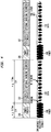
- FIG. 4 is a diagram illustrating the signal observed at the implantable receiver circuit 380 during power time slots 335 and data time slots 337.
- the power time slots 335 are approximately 0.5 milliseconds (ms) in length
- the data time slots are approximately 1.5 ms in length (i.e., the power time slots 335 occupy approximately 1 ⁇ 4 of the time while the data time slots 337 occupy approximately 3 ⁇ 4 of the time).
- the implant voltage (VDD) at load 383 is represented in FIG. 4 as dotted line 386.
- the implantable receiver circuit 380 receives all '1' signals.
- ringing is observed at the implantable receiver circuit 380. This ringing is a result of the high quality factor and efficiency of the external resonant tank circuit 325 during transmission of the power signals 388.
- the ringing is eliminated by reducing the quality factor of the external resonant tank circuit 325.
- the peak amplitude of the data signals 410 is reduced from the peak amplitude of the power signals 408. As shown in FIG. 4 , the peak amplitude of the data signals 410 is reduced so as to stay below the implant voltage 486 so that the implant voltage is not observed during the data time slots 337 (i.e., so that the diode 384 remains in reverse polarization).
- the data time slots 337 may not be fully filled (i.e., the number of signals sent may depend on the amount of data that needs to be transferred from the external component to the implantable component). In certain embodiments, all or part of a data time slot 337 may be used for backlink telemetry where data is sent from the implantable component to the external component.
- the external transmitter circuit 320 and the implantable receiver circuit 380 are, in practice, both transceiver circuits.
- FIG. 5 is a schematic diagram illustrating another external transmitter circuit 520 configured to separately transfer power and data signals to an implantable component via a single external coil 522 in accordance with embodiments presented herein. Similar to the embodiment of FIG. 3 , the external transmitter circuit 520 uses dedicated driver bridges for each of data and power transmission (i.e., the data and power signals have their own driver bridges and only a single driver bridge is enabled at a time). However, as described further below, the separate driver bridges are driven differently than as shown in FIG. 3 .
- the external transmitter circuit 520 comprises a first driver bridge 540 (data driver bridge) and a second driver bridge 541 (power driver bridge) that are each separately connected to the external coil 522.
- the external coil 522 is part of an external resonant tank circuit 525 that also comprises capacitor 542 (capacitor C1) and capacitor 544 (capacitor C2).
- external coil 522 has an inductive component (L HPC ) 546 and some small copper losses represented as the series resistive component (R HPC ) 548.
- the driver bridge 540 includes an input 550 that receives an input signal 531 via input signal line 552 and an enable input 553 that receives an enable signal 529 via enable signal line 555. As described further below, the enable input 553 is an inverting input.
- the driver bridge 540 also comprises a first output 554 and a second output 556.
- the first output 554 is connected to capacitor 542 (which is connected to external coil 522) via a series circuit 557 that comprises a resistor 558 (R1) in series with an inductor 560 (L1).
- the second output 556 is connected to capacitor 544 (which is also connected to external coil 522) via a series circuit 561 that comprises resistor 562 (R2) in series with an inductor 564 (L2).
- the driver bridge 541 includes an input 569 that receives the signal 531 via input line 552.
- the driver bridge 541 also comprises an enable input 573 configured to receive the enable signal 529 via enable signal line 555.
- the driver bridge 541 is connected to the same input signal line and the same enable signal as the driver bridge 540.
- the driver bridge 541 also comprises a first output 574 and a second output 576.
- the first output 574 is directly connected to capacitor 542 (which is connected to external coil 522) so as to bypass series circuit 557.
- the second output 576 is directly connected to capacitor 544 so as to bypass series circuit 561.
- the input signal 531 is a series of all '1' values or consecutive RF cycles during a power time slot 535. However, during a data time slot 537, the input signal 531 switches between '1s' and '0s' (i.e., is a digital code representing the OOK modulation).
- the enable signal 529 is a logic signal that alternatives between a value of '1' and '0'. The enable signal 529 has a vale of '1' during the power time slots 535 and a value of '0' during the data time slots 537.
- the enable signal 529 is high (i.e., a '1' value) so as to enable driver bridge 541.
- the outputs 574 and 576 generated using input signal 531, are used to drive external coil 522.
- the input 553 of driver bridge 540 is an inverting input. Therefore, when the enable signal 529 is high, the inverting input 553 will cause the driver bridge 540 to interpret the enable signal 529 as low (i.e., '0' value). This causes the outputs 554 and 556 of driver bridge 540 to be placed in a high impedance state.
- the enable signal 529 is low so as to cause the outputs 574 and 576 of driver bridge 541 to be placed in a high impedance state.
- the inverting input 553 will cause the driver bridge 540 to interpret the enable signal 529 as a high value.
- the outputs 554 and 556, generated using input signal 531, are used to drive external coil 522.
- the first output 554 is connected to external coil 522 via series circuit 557 (R1 and L1) and the second output 556 is connected to external coil 522 via series circuit 561 (R2 and L2).
- driver bridge 540 when driver bridge 540 is enabled, the external coil 522 is driven with signals that pass through series circuit 557 and series circuit 561.
- the bridge 541 is enabled to drive the external coil 522 with signals that pass directly from the outputs 574 and 576 to capacitors 542 and 544, respectively.
- the signals bypass the series circuits 557 (R1 and L1) and 561 (R2 and L2), thereby ensuring that the quality factor and resonant frequency of the external resonant tank circuit 525 are not affected by the series circuits 557 and 561.
- the driver bridge 350 is enabled so as to drive external coil 522 with signals that pass through the series circuit 557 (R1 and L1) and series circuit 561 (R2 and L2). That is, the series circuit 557 (R1 and L1) and series circuit 561 (R2 and L2) are placed in between the driver bridge 540 and the external coil 522.
- Driving the external coil 522 via the series circuits 557 and 561 causes a drop in (i.e., damp) the quality factor of the resonant tank circuit 525, the external coil current, and the resonance frequency.
- the quality factor of the resonant tank circuit 525 is maximized during power transmission, but is purposely lowered during data transmission (i.e., Q ext_data_timeslot ⁇ Q ext_power_timeslot ).
- the dampened external resonant tank circuit 525 reduces the ringing effects during one or more '0' cycle transitions after a sequence of '1' cycles during use of OOK modulation at f 0 .
- the series resistors 558 and 562 operate to dampen the external resonant tank circuit 525 when connected in series between the between the driver bridge 540 and the external coil 522.
- the external coil current drops during the data time slot when the external resonant tank circuit 525 is tuned lower than the operating frequency.
- the decrease in the external coil current prevents interference of the implantable component load with the data recovery at the implantable component.
- the operating frequency of the external coil 522 is 5 MHz and the resonant frequency of the external resonant tank circuit 525 during data transmission ( f res_data_timeslot ) is set equal to 4.75 MHz).
- the series inductors 560 and 564 operate to reduce the resonant frequency of the external resonant tank circuit 525 when connected in series between the between the driver bridge 540 and the external coil 522.
- FIG. 6 is simplified schematic diagram illustrating another external transmitter circuit 620 configured to separately transfer power and data signals to an implantable component via a single external coil 622 in accordance with embodiments presented herein. Similar to the embodiment of FIG. 5 , the external transmitter circuit 620 uses dedicated driver bridges for each of data and power transmission. However, in the embodiment of FIG. 6 , two (2) bridges are dedicated for use during power time slots, while a single separate driver bridge is used during the data time slots.
- the external transmitter circuit 620 comprises a data driver bridge 640 and two power driver bridges 641(1) and 641(2).
- the external coil 622 is part of an external resonant tank circuit 625 that comprises capacitors 642 (capacitors C1, C2, and C3).
- the driver bridges 640, 641(1), and 641(2) receive an input signal 531 (described above with reference to FIG. 5 ) and an enable signal 529 (also described above with reference to FIG. 5 ).
- the enable signal 529 is inverted before reaching data bridge 640.
- the driver bridge 640 may be a half H-bridge driver, while the driver bridges 641(1) and 641(2) may be full H-bridge drivers.
- the full H-bridge drivers 641(1) and 641(2) are activated and the outputs of the full H-bridge drivers are used to drive the external coil 622.
- the half H-bridge driver 640 is deactivated and the outputs of the half H-bridge driver are placed in a high impedance state. Placing the full H-bridge drivers 641(1) and 641(2) in parallel to operate simultaneously lowers the conductive losses at the output (relative to a single driver arrangement), thereby further increasing the quality factor of the tank circuit.
- the half H-bridge driver 640 is activated and the outputs of the half H-bridge driver are used to drive the external coil 622.
- a resistor 658 and an inductor 660 are connected between the outputs of the half H-bridge driver 640 and the external coil 622. The positioning of the resistor 658 and an inductor 660 between the half H-bridge driver 640 and the external coil 622 during data transmission will (1) dampen the resonant tank circuit 625 as described above and (2) lower the signal level of the data pulses received by the implant resulting in a non-conducting energy rectifier as described above.
- FIG. 6 illustrates a switch 605 that is closed when data is received at the external transmitter circuit 620 from an implantable component.
- the switch 605 bypasses the unidirectional driver bridges 640, 641(1), and 641(2) during backlink telemetry.
- Similar switches may be present in the embodiments of FIGS. 2A , 3 , 4 , and 5 , but have been omitted from those FIGS. for ease of illustration.
- the quality factor of the resonant tank circuit 625 is maximized during power transmission because the outputs of the full H-bridge drivers 641(1) and 641(2) are directly connected to the resonant tank circuit 625.
- the quality factor of the resonant tank circuit 625 is purposely lowered during data transmission.
- the dampened external resonant tank circuit 625 reduces the ringing effects during one or more '0' cycle transitions after a sequence of '1' cycles during use of OOK modulation at f o .
- the resistor 658 operates to dampen the external resonant tank circuit 625 when connected in series between the between the driver bridge 640 and the external coil 622.
- the external resonant tank circuit 625 is tuned lower than the operating frequency. As described elsewhere herein, the decrease in the external coil current prevents interference of the implantable component load with the data recovery at the implantable component.
- the operating frequency of the external coil 622 is 5 MHz and the resonant frequency of the external resonant tank circuit 625 during data transmission ( f res_data_timeslot ) is set equal to 4.75 MHz).
- the inductor 660 operates to reduce the resonant frequency of the external resonant tank circuit 625 when connected in series between the between the driver bridge 640 and the external coil 622.
- Embodiments have been primarily described above with reference to adjustments to the operational characteristics of an external resonant tank circuit. However, it is to be appreciated that adjustments to the operational characteristics of an implantable (internal) resonant tank circuit may be made in addition to, or in place of, the above adjustments to an external resonant tank circuit during the separated power and data transfer techniques.
- FIG. 7 illustrates an implantable receiver circuit 780 configured to receive separate power and data signals transmitted by an external transmitter circuit (not shown).
- the implantable receiver circuit 780 comprises an implantable coil 782 that is part of an implantable (internal) resonant tank circuit 785 that also comprises capacitor 794 (capacitor C4) and capacitor 796 (capacitor C5).
- implantable coil 792 has an inductive component (LI PC ) 777 and some small copper losses represented as the series resistive component (RI PC ) 779.
- LI PC inductive component
- RI PC series resistive component
- the implantable receiver circuit 780 also comprises a data output 781, a load 783 (i.e., battery or other energy storage device) connected between a power terminal 785 and a ground terminal 787, and an energy rectifier 784 connected between the implantable coil 782 and the load 783.
- the energy rectifier 784 is a diode.
- the implantable receiver circuit 780 also comprises a resistor 798 and a switch 799 connected in parallel to the capacitor 794.
- the switch 799 is closed.
- the resistor 798 is connected to the implantable resonant tank circuit 785.
- the resistor 798 operates to dampen the implantable resonant tank circuit 785. In other words, the resistor 798 functions to reduce the quality factor of the implantable resonant tank circuit 785 during data reception.
- a method for transmitting power from an external transmitter circuit to an implantable receiver circuit comprises an external resonant circuit that includes an external coil, while the implantable receiver circuit comprise an implantable resonant circuit that includes an implantable coil.
- the method comprises driving the external resonant circuit with one or more driver bridges during a power time slot to cause the external coil to transfer power to the implantable receiver circuit.
- the method further comprises driving the external resonant circuit with one or more driver bridges during a data time slot to cause the external coil to transfer data to the implantable receiver circuit.
- the power and data time slots are different time slots and the external resonant circuit is driven such that the quality factor of the external resonant circuit is lower during the data slot than during the power time slot.
- the the external resonant circuit and the implantable resonant circuit are resonant tank circuits.
- the method further comprises driving the external resonant circuit with one or more driver bridges during the data time slot such that a resonance frequency of the external resonant circuit is adjusted during the data time slot so as to be lower or higher than the resonant frequency of the external circuit during the power time slots.
- the method further comprises driving the external resonant circuit with one or more driver bridges during the data time slot such that a peak amplitude of current used to drive the external coil during the data time slots is lower than a peak amplitude of current used to drive the external coil during the power time slots.
- the implantable receiver circuit comprises an energy rectifier and the method further comprises driving the external resonant circuit with one or more driver bridges during the data time slot such that the peak amplitude of current used to drive the external during the data time slot is such that the energy rectifier does not allow current to pass there through during the data time slots.
- the external coil is part of an external resonant tank circuit, while the implantable coil is part of an implantable resonant tank circuit.
- the external coil is configured to transcutaneously transfer power and data to the implantable coil using separate power and data time slots. At least one of the external or internal resonant tank circuit is substantially more damped during the data time slot than during the power time slot.
- High efficiently power transfers may reduce the number of implantable batteries needed, increase autonomy of the implantable component, and enable use of implantable components with larger skin flaps
- the data link can be considered as a Magnetic Induction (MI) radio system over, for example, 5MHz and could accept data from the bilateral implant during the data time slot. Additionally, ringing effects are substantially eliminated during data transfer due to the damped external tank circuit.
- MI Magnetic Induction
- the techniques presented herein may also provide stable waveforms shapes during data time slots received by the implant and almost independent of coupling factor, implant load, data time slot duration or frame occupation.
- the data link can support other modulation types.
- amplitude ringing is a phenomena typically observed in OOK modulation
- other modulation types such as FSK or PSK may also suffer from excessive phase ringing or distortion due to insufficient dampening during the data time slot.
Landscapes
- Health & Medical Sciences (AREA)
- Engineering & Computer Science (AREA)
- Biomedical Technology (AREA)
- Nuclear Medicine, Radiotherapy & Molecular Imaging (AREA)
- Radiology & Medical Imaging (AREA)
- Life Sciences & Earth Sciences (AREA)
- Animal Behavior & Ethology (AREA)
- General Health & Medical Sciences (AREA)
- Public Health (AREA)
- Veterinary Medicine (AREA)
- Computer Networks & Wireless Communication (AREA)
- Power Engineering (AREA)
- Otolaryngology (AREA)
- Physics & Mathematics (AREA)
- Electromagnetism (AREA)
- Acoustics & Sound (AREA)
- Signal Processing (AREA)
- Near-Field Transmission Systems (AREA)
- Electrotherapy Devices (AREA)
- Arrangements For Transmission Of Measured Signals (AREA)
- Prostheses (AREA)
Claims (14)
- Implantierbares medizinisches Gerät, das umfasst:einen implantierbaren Resonanzschaltkreis (385, 785), der eine implantierbare Spule (382,782) umfasst; undeinen externen Resonanzschaltkreis (225, 325, 525, 625), der eine externe Spule (222, 322, 522, 622) umfasst, die konfiguriert ist, transkutan Energie und Daten an die implantierbare Spule unter Verwendung getrennter Energie- und DatenZeitfenster zu übertragen,wobei eine Stromspitzenamplitude, die verwendet wird, die externe Spule (222, 322, 522, 622) während dem Datenzeitfenster anzusteuern, kleiner ist als eine Stromspitzenamplitude, die verwendet wird, die externe Spule (222, 322, 522, 622) während dem Energiezeitfenster anzusteuern, undwobei zumindest der externe oder der implantierbare Resonanzschaltkreis während dem Datenzeitfenster im Wesentlichen stärker gedämpft ist als während dem Energiezeitfenster,dadurch gekennzeichnet, dassdas implantierbare medizinische Gerät konfiguriert ist, den externen Resonanzschaltkreis (225, 325, 525, 625) mit einem oder mehreren Treiberbrücken während dem Datenzeitfenster so anzusteuern, dass die Resonanzfrequenz des externen Resonanz Schaltkreises (225, 325, 525, 625) so eingestellt wird, dass sie geringer oder höher ist als die Resonanzfrequenz des externen Schaltkreises während dem Energiezeitfenster.
- Implantierbares medizinisches Gerät nach Anspruch 1, wobei der externe und der implantierbare Resonanzschaltkreis Resonanzschwingkreise sind.
- Implantierbares medizinisches Gerät nach Anspruch 1, wobei eine Resonanzfrequenz des externen Resonanzschaltkreises während dem Datenzeitfenster so eingestellt wird, dass sie kleiner oder größer ist als die Resonanzfrequenz des externen Schaltkreises während dem Energiezeitfenster.
- Implantierbares medizinisches Gerät nach Anspruch 1, wobei die implantierbare Spule an einem Energiegleichrichter angeschlossen ist, und wobei die Stromspitzenamplitude, die verwendet wird, um die externe Spule während dem Datenzeitfenster anzutreiben, so ist, dass der Energiegleichrichter nicht zulässt, dass Strom während dem Datenzeitfenster durchfließt.
- Implantierbares medizinisches Gerät nach Anspruch 1, wobei der externe Resonanzschaltkreis mit einer Treiberbrücke verbunden ist, die verwendet wird, die externe Spule während sowohl dem Energiezeitfenster als auch dem Datenzeitfenster anzusteuern.
- Implantierbares medizinisches Gerät nach Anspruch 5, das weiterhin umfasst:einen ersten Reihenschaltkreis, der einen ersten Widerstand und eine erste Spule umfasst, die zwischen einem ersten Ausgang der Treiberbrücke und dem externen Resonanzschaltkreis verbunden ist;einen zweiten Reihenschaltkreis, der einen zweiten Widerstand und eine zweite Spule umfasst, die zwischen einem zweiten Ausgang der Treiberbrücke und dem externen Resonanzschaltkreis verbunden ist; undeinen Schalter, der parallel zum ersten und zweiten Reihenschaltkreis zwischen dem ersten und dem zweiten Ausgang der Treiberbrücke und dem externen Resonanzschaltkreis angeschlossen ist,wobei der Schalter während dem Datenzeitfenster offen ist, so dass Signale vom ersten und zweiten Ausgang der Treiberbrücke durch den ersten bzw. zweiten Reihenschaltkreis durchgehen, und wobei der Schalter während dem Energiezeitfenster geschlossen ist, so dass die Signale von dem ersten und zweiten Ausgang der Treiberbrücke den ersten und zweiten Reihenschaltkreis umgehen.
- Implantierbares medizinisches Gerät nach Anspruch 1, wobei der Resonanzschaltkreis mit zwei oder mehr Treiberbrücken verbunden ist, wobei unterschiedliche Treiberbrücken verwendet werden, um die Spule während dem Energie- bzw. dem Datenzeitfenster anzusteuern.
- Implantierbares medizinisches Gerät nach Anspruch 7, wobei eine erste Treiberbrücke eine halbe H-Brücke ist und die mindestens eine zusätzliche Treiberbrücke eine volle H-Brücke ist.
- Implantierbares medizinisches Gerät nach Anspruch 7, wobei Ausgänge einer Treiberbrücke, die während dem Energiezeitfenster oder dem Datenzeitfenster nicht verwendet werden, in einen Zustand hoher Impedanz versetzt werden.
- Implantierbares medizinisches Gerät nach Anspruch 7, wobei eine erste fest zugewiesene Treiberbrücke während dem Datenzeitfenster aktiviert wird und eine zweite fest zugewiesene Treiberbrücke während dem Energiezeitfenster aktiviert wird.
- Implantierbares medizinisches Gerät nach Anspruch 7, das weiterhin umfasst:eine Datentreiberbrücke;einen ersten Reihenschaltkreis, der einen ersten Widerstand und eine erste Spule umfasst, die zwischen einem ersten Ausgang der Datentreiberbrücke und dem externen Resonanzschaltkreises verbunden ist;einen zweiten Reihenschaltkreis, der einen zweiten Widerstand und eine zweite Spule umfasst, die zwischen einem zweiten Ausgang der Datentreiberbrücke und dem externen Resonanzschaltkreises verbunden ist; undmindestens eine Energietreiberbrücke, die direkt mit dem externen Resonanzschaltkreis verbunden ist, um so den ersten und zweiten Reihenschaltkreis zu umgehen,wobei die Datentreiberbrücke während dem Datenzeitfenster aktiviert ist und Ausgänge der mindestens einen Energietreiberbrücke in einen Zustand hoher Impedanz versetzt werden, und wobei die mindestens eine Energietreiberbrücke während dem Energiezeitfenster aktiviert ist und die ersten und zweiten Ausgänge der Datentreiberbrücke in einen Zustand hoher Impedanz versetzt werden.
- Implantierbares medizinisches Gerät nach Anspruch 11, wobei die mindestens eine Energietreiberbrücke eine erste und eine zweite Energietreiberbrücke umfasst, die konfiguriert sind, gleichzeitig aktiviert zu werden.
- Implantierbares medizinisches Gerät nach Anspruch 1, das weiterhin umfasst:einen Kondensator, der mit der implantierbaren Spule verbunden ist und der einen Teil des implantierbaren Resonanzschaltkreises bildet; undeinen Widerstand, der über einen implantierbaren Schalter parallel zum Kondensator verbindbar ist,wobei der implantierbare Schalter während dem Datenzeitfenster geschlossen ist, um so den Widerstand mit dem implantierbaren Resonanzschaltkreis zu verbinden, um den implantierbaren Resonanzschaltkreis zu dämpfen, und wobei der implantierbare Schalter während dem Energiezeitfenster geöffnet ist, um so den Widerstand von dem implantierbaren Resonanzschaltkreises abzutrennen.
- Implantierbares medizinisches Gerät nach Anspruch 1, wobei der Qualitätsfaktor des externen Resonanzschaltkreises während dem Datenfenster kleiner ist als während dem Energiezeitfenster.
Applications Claiming Priority (3)
| Application Number | Priority Date | Filing Date | Title |
|---|---|---|---|
| US201461933512P | 2014-01-30 | 2014-01-30 | |
| US14/542,877 US9724525B2 (en) | 2014-01-30 | 2014-11-17 | Power and data transfer in hearing prostheses |
| PCT/IB2015/050694 WO2015114571A1 (en) | 2014-01-30 | 2015-01-29 | Power and data transfer in hearing prostheses |
Publications (3)
| Publication Number | Publication Date |
|---|---|
| EP3100468A1 EP3100468A1 (de) | 2016-12-07 |
| EP3100468A4 EP3100468A4 (de) | 2017-09-13 |
| EP3100468B1 true EP3100468B1 (de) | 2019-08-21 |
Family
ID=53678079
Family Applications (1)
| Application Number | Title | Priority Date | Filing Date |
|---|---|---|---|
| EP15743022.4A Active EP3100468B1 (de) | 2014-01-30 | 2015-01-29 | Leistungs- und datenübertragung bei hörprothesen |
Country Status (6)
| Country | Link |
|---|---|
| US (4) | US9724525B2 (de) |
| EP (1) | EP3100468B1 (de) |
| KR (1) | KR102450304B1 (de) |
| CN (1) | CN105917673B (de) |
| AU (1) | AU2015212353B2 (de) |
| WO (1) | WO2015114571A1 (de) |
Cited By (6)
| Publication number | Priority date | Publication date | Assignee | Title |
|---|---|---|---|---|
| WO2022006009A1 (en) | 2020-06-28 | 2022-01-06 | Nucurrent, Inc. | Higher power high frequency wireless power transfer system |
| US12199700B2 (en) | 2021-01-28 | 2025-01-14 | Nucurrent, Inc. | Wireless power transmission systems and methods with selective signal damping at periodic active mode windows |
| US12244159B2 (en) | 2020-06-28 | 2025-03-04 | Nucurrent, Inc. | Wireless power transmitter for high fidelity communications and high power transfer |
| US12289141B2 (en) | 2021-01-28 | 2025-04-29 | Nucurrent, Inc. | Wireless power transmitter for high fidelity communications with amplitude shift keying |
| US12301305B2 (en) | 2021-01-28 | 2025-05-13 | Nucurrent, Inc. | Wireless power transmitter for high fidelity communications at high power transfer |
| US12614928B2 (en) | 2024-03-25 | 2026-04-28 | Nucurrent, Inc. | Wireless charging in eyewear with enhanced positional freedom |
Families Citing this family (20)
| Publication number | Priority date | Publication date | Assignee | Title |
|---|---|---|---|---|
| DE102015112098A1 (de) | 2014-07-25 | 2016-01-28 | Minnetronix, Inc. | Spulenparameter und Steuerung |
| US9855376B2 (en) | 2014-07-25 | 2018-01-02 | Minnetronix, Inc. | Power scaling |
| US10342908B2 (en) | 2015-01-14 | 2019-07-09 | Minnetronix, Inc. | Distributed transformer |
| DE102016100534A1 (de) | 2015-01-16 | 2016-07-21 | Vlad BLUVSHTEIN | Datenübertragung in einem transkutanen Energieübertragungssystem |
| US10193395B2 (en) | 2015-04-14 | 2019-01-29 | Minnetronix, Inc. | Repeater resonator |
| WO2017072674A1 (en) * | 2015-10-27 | 2017-05-04 | Cochlear Limited | Inductance coil with varied geometry |
| US10425751B2 (en) | 2015-12-18 | 2019-09-24 | Cochlear Limited | Dual power supply |
| JP6757260B2 (ja) * | 2017-01-12 | 2020-09-16 | ホシデン株式会社 | 非接触送信モジュール、これを備えた非接触通信システムおよび非接触通信方法 |
| US10864379B2 (en) | 2017-03-22 | 2020-12-15 | Cochlear Limited | Autonomous implantable medical device tuning |
| CN111295895B (zh) * | 2017-10-23 | 2021-10-15 | 科利耳有限公司 | 一种身体穿戴装置、多用途装置和方法 |
| GB201721863D0 (en) * | 2017-12-24 | 2018-02-07 | Vivoplex Group Ltd | Monitoring system |
| US10418862B1 (en) | 2018-05-31 | 2019-09-17 | Advanced Bionics Ag | Systems and methods for wirelessly transmitting power and data from an active headpiece to a cochlear implant |
| US11251660B2 (en) | 2018-05-31 | 2022-02-15 | Advanced Bionics Ag | Systems and methods for wirelessly transmitting power and data to an implantable stimulator |
| US20200144480A1 (en) * | 2018-11-01 | 2020-05-07 | Northeastern University | Implantable Devices Based on Magnetoelectric Antenna, Energy Harvesting and Communication |
| EP3999169A4 (de) * | 2019-07-15 | 2023-09-06 | Cochlear Limited | Transkutane strom- und datenkommunikationsverbindung |
| US12290686B2 (en) * | 2019-09-17 | 2025-05-06 | Advanced Bionics Ag | Systems and devices for equalizing telemetry signals transmitted by way of a transcutaneous narrowband inductive link |
| FR3114710B1 (fr) | 2020-09-25 | 2024-07-26 | Neurinnov | Dispositif médical implantable actif |
| FR3114724B1 (fr) * | 2020-09-30 | 2023-11-10 | St Microelectronics Rousset | Dispositif et procédé de communication en champ proche |
| WO2024224272A1 (en) * | 2023-04-25 | 2024-10-31 | Cochlear Limited | Initialization protocol for implant radio frequency links |
| FR3153712B1 (fr) * | 2023-10-02 | 2025-10-31 | St Microelectronics Int Nv | Dispositif NFC |
Family Cites Families (27)
| Publication number | Priority date | Publication date | Assignee | Title |
|---|---|---|---|---|
| CA2235216C (en) | 1995-10-19 | 2006-05-30 | The University Of Melbourne | Embedded data link and protocol |
| DE19621076C2 (de) * | 1996-05-24 | 2001-06-28 | Siemens Ag | Vorrichtung und Verfahren zum kontaktlosen Übertragen von Energie oder Daten |
| WO2001080795A1 (en) | 2000-04-20 | 2001-11-01 | Cochlear Limited | Transcutaneous power optimization circuit for cochlear implant |
| US6591139B2 (en) * | 2000-09-06 | 2003-07-08 | Advanced Bionics Corporation | Low-power, high-modulation-index amplifier for use in battery-powered device |
| US7016738B1 (en) | 2002-07-31 | 2006-03-21 | Advanced Bionics Corporation | Digitally controlled RF amplifier with wide dynamic range output |
| US7580395B2 (en) * | 2002-11-29 | 2009-08-25 | Intermec Ip Corp. | Information gathering apparatus and method having multiple wireless communication options |
| US7623827B2 (en) * | 2003-10-20 | 2009-11-24 | Cochlear Limited | Voltage overshoot protection |
| NZ535390A (en) * | 2004-09-16 | 2007-10-26 | Auckland Uniservices Ltd | Inductively powered mobile sensor system |
| US7746921B1 (en) * | 2005-10-11 | 2010-06-29 | Thomas Robert Wik | Resonant digital data transmission |
| KR20060108251A (ko) | 2006-08-21 | 2006-10-17 | 장순석 | 귓속 보청기 |
| US9889307B2 (en) * | 2008-02-22 | 2018-02-13 | Cochlear Limited | Interleaving power and data in a transcutaneous communications link |
| WO2009124174A2 (en) * | 2008-04-02 | 2009-10-08 | Cochlear Americas | An adjustable transcutaneous energy transfer system |
| US20120112691A1 (en) * | 2008-09-27 | 2012-05-10 | Kurs Andre B | Wireless energy transfer for vehicles |
| US8335569B2 (en) * | 2009-02-10 | 2012-12-18 | Boston Scientific Neuromodulation Corporation | External device for communicating with an implantable medical device having data telemetry and charging integrated in a single housing |
| EP4234001A3 (de) * | 2009-03-09 | 2023-10-18 | NuCurrent, Inc. | System und verfahren für drahtlose leistungsübertragung bei implantierten medizinischen vorrichtungen |
| US9166655B2 (en) * | 2010-10-28 | 2015-10-20 | Cochlear Limited | Magnetic induction communication system for an implantable medical device |
| CN105490314B (zh) * | 2011-05-13 | 2019-04-26 | 三星电子株式会社 | 发送无线电力的发送器、接收无线电力的接收器、及方法 |
| WO2013009881A2 (en) * | 2011-07-11 | 2013-01-17 | Vascor, Inc. | Transcutaneous power transmission and communication for implanted heart assist and other devices |
| US20130043735A1 (en) * | 2011-08-16 | 2013-02-21 | Qualcomm Incorporated | Systems, methods, and devices for multi-level signaling via a wireless power transfer field |
| US8687831B2 (en) | 2011-10-27 | 2014-04-01 | Med-El Elektromedizinische Geraete Gmbh | Optimized energy and data transfer in hearing implant systems |
| US20130123881A1 (en) * | 2011-11-11 | 2013-05-16 | Boston Scientific Neuromodulation Corporation | External Charger for an Implantable Medical Device System Having a Coil for Communication and Charging |
| US9744368B2 (en) * | 2012-02-16 | 2017-08-29 | Medtronic, Inc. | Self-tuning external device for wirelessly recharging implantable medical devices |
| US8827889B2 (en) * | 2012-05-21 | 2014-09-09 | University Of Washington Through Its Center For Commercialization | Method and system for powering implantable devices |
| DK2675189T3 (en) * | 2012-06-14 | 2015-11-09 | Oticon As | Binaural listening system with automatic mode can |
| US20140021909A1 (en) * | 2012-07-19 | 2014-01-23 | Barnesandnoble.Com Llc | Charging case for electronic devices |
| US20140214123A1 (en) | 2013-01-28 | 2014-07-31 | Jan Janssen | Bilateral Communication in a Two-Channel System |
| CN203233402U (zh) * | 2013-05-21 | 2013-10-09 | 谭丽萍 | 宽带脉冲发射器 |
-
2014
- 2014-11-17 US US14/542,877 patent/US9724525B2/en active Active
-
2015
- 2015-01-29 EP EP15743022.4A patent/EP3100468B1/de active Active
- 2015-01-29 CN CN201580004517.0A patent/CN105917673B/zh active Active
- 2015-01-29 KR KR1020167019559A patent/KR102450304B1/ko active Active
- 2015-01-29 AU AU2015212353A patent/AU2015212353B2/en active Active
- 2015-01-29 WO PCT/IB2015/050694 patent/WO2015114571A1/en not_active Ceased
-
2017
- 2017-05-12 US US15/593,576 patent/US10632317B2/en active Active
-
2020
- 2020-03-30 US US16/834,053 patent/US11577087B2/en active Active
-
2023
- 2023-01-12 US US18/153,638 patent/US12246186B2/en active Active
Non-Patent Citations (1)
| Title |
|---|
| None * |
Cited By (7)
| Publication number | Priority date | Publication date | Assignee | Title |
|---|---|---|---|---|
| WO2022006009A1 (en) | 2020-06-28 | 2022-01-06 | Nucurrent, Inc. | Higher power high frequency wireless power transfer system |
| EP4173113A4 (de) * | 2020-06-28 | 2025-01-01 | NuCurrent, Inc. | Hochfrequentes drahtloses stromübertragungssystem mit höherer leistung |
| US12244159B2 (en) | 2020-06-28 | 2025-03-04 | Nucurrent, Inc. | Wireless power transmitter for high fidelity communications and high power transfer |
| US12199700B2 (en) | 2021-01-28 | 2025-01-14 | Nucurrent, Inc. | Wireless power transmission systems and methods with selective signal damping at periodic active mode windows |
| US12289141B2 (en) | 2021-01-28 | 2025-04-29 | Nucurrent, Inc. | Wireless power transmitter for high fidelity communications with amplitude shift keying |
| US12301305B2 (en) | 2021-01-28 | 2025-05-13 | Nucurrent, Inc. | Wireless power transmitter for high fidelity communications at high power transfer |
| US12614928B2 (en) | 2024-03-25 | 2026-04-28 | Nucurrent, Inc. | Wireless charging in eyewear with enhanced positional freedom |
Also Published As
| Publication number | Publication date |
|---|---|
| AU2015212353A1 (en) | 2016-07-21 |
| US20150209591A1 (en) | 2015-07-30 |
| US10632317B2 (en) | 2020-04-28 |
| KR20160114591A (ko) | 2016-10-05 |
| WO2015114571A1 (en) | 2015-08-06 |
| EP3100468A4 (de) | 2017-09-13 |
| AU2015212353B2 (en) | 2019-04-18 |
| US12246186B2 (en) | 2025-03-11 |
| US20230166117A1 (en) | 2023-06-01 |
| EP3100468A1 (de) | 2016-12-07 |
| US20200222701A1 (en) | 2020-07-16 |
| US11577087B2 (en) | 2023-02-14 |
| US20170246462A1 (en) | 2017-08-31 |
| CN105917673B (zh) | 2019-12-10 |
| CN105917673A (zh) | 2016-08-31 |
| US9724525B2 (en) | 2017-08-08 |
| KR102450304B1 (ko) | 2022-09-30 |
Similar Documents
| Publication | Publication Date | Title |
|---|---|---|
| US12246186B2 (en) | Power and data transfer in hearing prostheses | |
| US8996121B2 (en) | Varying the effective coil area for an inductive transcutaneous power link | |
| US9166655B2 (en) | Magnetic induction communication system for an implantable medical device | |
| US12476037B2 (en) | Inductance coil path | |
| US11272300B2 (en) | Dual power supply | |
| WO2009137204A2 (en) | Transceiver for an implantable medical device having switchable series-to-parallel tank circuit | |
| US20250381399A1 (en) | Transcutaneous power and data communication link | |
| US12539429B2 (en) | Autonomous implantable medical device tuning | |
| US10265533B2 (en) | Implant heat protection | |
| US20230405347A1 (en) | Quantized waveform power transmission | |
| WO2023105357A1 (en) | Charging device for implant | |
| US12329980B2 (en) | Medical device component with dual-band coil assembly | |
| US20250367458A1 (en) | Load modulation detector | |
| US11679267B1 (en) | Medical implant with stimulation leakage current blocking | |
| US10397715B2 (en) | System and method for improving data integrity and power efficiency | |
| WO2024231777A1 (en) | Active coil damping |
Legal Events
| Date | Code | Title | Description |
|---|---|---|---|
| PUAI | Public reference made under article 153(3) epc to a published international application that has entered the european phase |
Free format text: ORIGINAL CODE: 0009012 |
|
| STAA | Information on the status of an ep patent application or granted ep patent |
Free format text: STATUS: REQUEST FOR EXAMINATION WAS MADE |
|
| 17P | Request for examination filed |
Effective date: 20160728 |
|
| AK | Designated contracting states |
Kind code of ref document: A1 Designated state(s): AL AT BE BG CH CY CZ DE DK EE ES FI FR GB GR HR HU IE IS IT LI LT LU LV MC MK MT NL NO PL PT RO RS SE SI SK SM TR |
|
| AX | Request for extension of the european patent |
Extension state: BA ME |
|
| DAX | Request for extension of the european patent (deleted) | ||
| A4 | Supplementary search report drawn up and despatched |
Effective date: 20170811 |
|
| RIC1 | Information provided on ipc code assigned before grant |
Ipc: A61N 1/372 20060101ALI20170807BHEP Ipc: A61N 1/378 20060101AFI20170807BHEP Ipc: H02J 5/00 20160101ALN20170807BHEP Ipc: H02J 7/02 20160101ALN20170807BHEP Ipc: H04R 25/00 20060101ALN20170807BHEP Ipc: H02J 50/12 20160101ALI20170807BHEP |
|
| STAA | Information on the status of an ep patent application or granted ep patent |
Free format text: STATUS: EXAMINATION IS IN PROGRESS |
|
| 17Q | First examination report despatched |
Effective date: 20180727 |
|
| REG | Reference to a national code |
Ref country code: DE Ref legal event code: R079 Ref document number: 602015036278 Country of ref document: DE Free format text: PREVIOUS MAIN CLASS: H04R0025000000 Ipc: A61N0001378000 |
|
| GRAP | Despatch of communication of intention to grant a patent |
Free format text: ORIGINAL CODE: EPIDOSNIGR1 |
|
| STAA | Information on the status of an ep patent application or granted ep patent |
Free format text: STATUS: GRANT OF PATENT IS INTENDED |
|
| RIC1 | Information provided on ipc code assigned before grant |
Ipc: H02J 50/12 20160101ALI20190220BHEP Ipc: H04R 25/00 20060101ALN20190220BHEP Ipc: H02J 5/00 20160101ALN20190220BHEP Ipc: H02J 50/80 20160101ALN20190220BHEP Ipc: H02J 7/02 20160101ALN20190220BHEP Ipc: A61N 1/36 20060101ALN20190220BHEP Ipc: A61N 1/372 20060101ALI20190220BHEP Ipc: A61N 1/378 20060101AFI20190220BHEP |
|
| INTG | Intention to grant announced |
Effective date: 20190306 |
|
| RIN1 | Information on inventor provided before grant (corrected) |
Inventor name: MESKENS, WERNER |
|
| GRAS | Grant fee paid |
Free format text: ORIGINAL CODE: EPIDOSNIGR3 |
|
| GRAA | (expected) grant |
Free format text: ORIGINAL CODE: 0009210 |
|
| STAA | Information on the status of an ep patent application or granted ep patent |
Free format text: STATUS: THE PATENT HAS BEEN GRANTED |
|
| AK | Designated contracting states |
Kind code of ref document: B1 Designated state(s): AL AT BE BG CH CY CZ DE DK EE ES FI FR GB GR HR HU IE IS IT LI LT LU LV MC MK MT NL NO PL PT RO RS SE SI SK SM TR |
|
| REG | Reference to a national code |
Ref country code: GB Ref legal event code: FG4D |
|
| REG | Reference to a national code |
Ref country code: CH Ref legal event code: EP |
|
| REG | Reference to a national code |
Ref country code: DE Ref legal event code: R096 Ref document number: 602015036278 Country of ref document: DE |
|
| REG | Reference to a national code |
Ref country code: AT Ref legal event code: REF Ref document number: 1169027 Country of ref document: AT Kind code of ref document: T Effective date: 20190915 |
|
| REG | Reference to a national code |
Ref country code: IE Ref legal event code: FG4D |
|
| REG | Reference to a national code |
Ref country code: LT Ref legal event code: MG4D |
|
| REG | Reference to a national code |
Ref country code: NL Ref legal event code: MP Effective date: 20190821 |
|
| PG25 | Lapsed in a contracting state [announced via postgrant information from national office to epo] |
Ref country code: PT Free format text: LAPSE BECAUSE OF FAILURE TO SUBMIT A TRANSLATION OF THE DESCRIPTION OR TO PAY THE FEE WITHIN THE PRESCRIBED TIME-LIMIT Effective date: 20191223 Ref country code: NO Free format text: LAPSE BECAUSE OF FAILURE TO SUBMIT A TRANSLATION OF THE DESCRIPTION OR TO PAY THE FEE WITHIN THE PRESCRIBED TIME-LIMIT Effective date: 20191121 Ref country code: SE Free format text: LAPSE BECAUSE OF FAILURE TO SUBMIT A TRANSLATION OF THE DESCRIPTION OR TO PAY THE FEE WITHIN THE PRESCRIBED TIME-LIMIT Effective date: 20190821 Ref country code: FI Free format text: LAPSE BECAUSE OF FAILURE TO SUBMIT A TRANSLATION OF THE DESCRIPTION OR TO PAY THE FEE WITHIN THE PRESCRIBED TIME-LIMIT Effective date: 20190821 Ref country code: LT Free format text: LAPSE BECAUSE OF FAILURE TO SUBMIT A TRANSLATION OF THE DESCRIPTION OR TO PAY THE FEE WITHIN THE PRESCRIBED TIME-LIMIT Effective date: 20190821 Ref country code: HR Free format text: LAPSE BECAUSE OF FAILURE TO SUBMIT A TRANSLATION OF THE DESCRIPTION OR TO PAY THE FEE WITHIN THE PRESCRIBED TIME-LIMIT Effective date: 20190821 Ref country code: NL Free format text: LAPSE BECAUSE OF FAILURE TO SUBMIT A TRANSLATION OF THE DESCRIPTION OR TO PAY THE FEE WITHIN THE PRESCRIBED TIME-LIMIT Effective date: 20190821 Ref country code: BG Free format text: LAPSE BECAUSE OF FAILURE TO SUBMIT A TRANSLATION OF THE DESCRIPTION OR TO PAY THE FEE WITHIN THE PRESCRIBED TIME-LIMIT Effective date: 20191121 |
|
| PG25 | Lapsed in a contracting state [announced via postgrant information from national office to epo] |
Ref country code: AL Free format text: LAPSE BECAUSE OF FAILURE TO SUBMIT A TRANSLATION OF THE DESCRIPTION OR TO PAY THE FEE WITHIN THE PRESCRIBED TIME-LIMIT Effective date: 20190821 Ref country code: ES Free format text: LAPSE BECAUSE OF FAILURE TO SUBMIT A TRANSLATION OF THE DESCRIPTION OR TO PAY THE FEE WITHIN THE PRESCRIBED TIME-LIMIT Effective date: 20190821 Ref country code: LV Free format text: LAPSE BECAUSE OF FAILURE TO SUBMIT A TRANSLATION OF THE DESCRIPTION OR TO PAY THE FEE WITHIN THE PRESCRIBED TIME-LIMIT Effective date: 20190821 Ref country code: RS Free format text: LAPSE BECAUSE OF FAILURE TO SUBMIT A TRANSLATION OF THE DESCRIPTION OR TO PAY THE FEE WITHIN THE PRESCRIBED TIME-LIMIT Effective date: 20190821 Ref country code: GR Free format text: LAPSE BECAUSE OF FAILURE TO SUBMIT A TRANSLATION OF THE DESCRIPTION OR TO PAY THE FEE WITHIN THE PRESCRIBED TIME-LIMIT Effective date: 20191122 Ref country code: IS Free format text: LAPSE BECAUSE OF FAILURE TO SUBMIT A TRANSLATION OF THE DESCRIPTION OR TO PAY THE FEE WITHIN THE PRESCRIBED TIME-LIMIT Effective date: 20191221 |
|
| REG | Reference to a national code |
Ref country code: AT Ref legal event code: MK05 Ref document number: 1169027 Country of ref document: AT Kind code of ref document: T Effective date: 20190821 |
|
| PG25 | Lapsed in a contracting state [announced via postgrant information from national office to epo] |
Ref country code: TR Free format text: LAPSE BECAUSE OF FAILURE TO SUBMIT A TRANSLATION OF THE DESCRIPTION OR TO PAY THE FEE WITHIN THE PRESCRIBED TIME-LIMIT Effective date: 20190821 |
|
| PG25 | Lapsed in a contracting state [announced via postgrant information from national office to epo] |
Ref country code: RO Free format text: LAPSE BECAUSE OF FAILURE TO SUBMIT A TRANSLATION OF THE DESCRIPTION OR TO PAY THE FEE WITHIN THE PRESCRIBED TIME-LIMIT Effective date: 20190821 Ref country code: PL Free format text: LAPSE BECAUSE OF FAILURE TO SUBMIT A TRANSLATION OF THE DESCRIPTION OR TO PAY THE FEE WITHIN THE PRESCRIBED TIME-LIMIT Effective date: 20190821 Ref country code: EE Free format text: LAPSE BECAUSE OF FAILURE TO SUBMIT A TRANSLATION OF THE DESCRIPTION OR TO PAY THE FEE WITHIN THE PRESCRIBED TIME-LIMIT Effective date: 20190821 Ref country code: AT Free format text: LAPSE BECAUSE OF FAILURE TO SUBMIT A TRANSLATION OF THE DESCRIPTION OR TO PAY THE FEE WITHIN THE PRESCRIBED TIME-LIMIT Effective date: 20190821 Ref country code: IT Free format text: LAPSE BECAUSE OF FAILURE TO SUBMIT A TRANSLATION OF THE DESCRIPTION OR TO PAY THE FEE WITHIN THE PRESCRIBED TIME-LIMIT Effective date: 20190821 Ref country code: DK Free format text: LAPSE BECAUSE OF FAILURE TO SUBMIT A TRANSLATION OF THE DESCRIPTION OR TO PAY THE FEE WITHIN THE PRESCRIBED TIME-LIMIT Effective date: 20190821 |
|
| PG25 | Lapsed in a contracting state [announced via postgrant information from national office to epo] |
Ref country code: IS Free format text: LAPSE BECAUSE OF FAILURE TO SUBMIT A TRANSLATION OF THE DESCRIPTION OR TO PAY THE FEE WITHIN THE PRESCRIBED TIME-LIMIT Effective date: 20200224 Ref country code: CZ Free format text: LAPSE BECAUSE OF FAILURE TO SUBMIT A TRANSLATION OF THE DESCRIPTION OR TO PAY THE FEE WITHIN THE PRESCRIBED TIME-LIMIT Effective date: 20190821 Ref country code: SM Free format text: LAPSE BECAUSE OF FAILURE TO SUBMIT A TRANSLATION OF THE DESCRIPTION OR TO PAY THE FEE WITHIN THE PRESCRIBED TIME-LIMIT Effective date: 20190821 Ref country code: SK Free format text: LAPSE BECAUSE OF FAILURE TO SUBMIT A TRANSLATION OF THE DESCRIPTION OR TO PAY THE FEE WITHIN THE PRESCRIBED TIME-LIMIT Effective date: 20190821 |
|
| REG | Reference to a national code |
Ref country code: DE Ref legal event code: R097 Ref document number: 602015036278 Country of ref document: DE |
|
| PLBE | No opposition filed within time limit |
Free format text: ORIGINAL CODE: 0009261 |
|
| STAA | Information on the status of an ep patent application or granted ep patent |
Free format text: STATUS: NO OPPOSITION FILED WITHIN TIME LIMIT |
|
| PG2D | Information on lapse in contracting state deleted |
Ref country code: IS |
|
| 26N | No opposition filed |
Effective date: 20200603 |
|
| PG25 | Lapsed in a contracting state [announced via postgrant information from national office to epo] |
Ref country code: MC Free format text: LAPSE BECAUSE OF FAILURE TO SUBMIT A TRANSLATION OF THE DESCRIPTION OR TO PAY THE FEE WITHIN THE PRESCRIBED TIME-LIMIT Effective date: 20190821 Ref country code: SI Free format text: LAPSE BECAUSE OF FAILURE TO SUBMIT A TRANSLATION OF THE DESCRIPTION OR TO PAY THE FEE WITHIN THE PRESCRIBED TIME-LIMIT Effective date: 20190821 |
|
| REG | Reference to a national code |
Ref country code: CH Ref legal event code: PL |
|
| REG | Reference to a national code |
Ref country code: BE Ref legal event code: MM Effective date: 20200131 |
|
| PG25 | Lapsed in a contracting state [announced via postgrant information from national office to epo] |
Ref country code: LU Free format text: LAPSE BECAUSE OF NON-PAYMENT OF DUE FEES Effective date: 20200129 |
|
| PG25 | Lapsed in a contracting state [announced via postgrant information from national office to epo] |
Ref country code: LI Free format text: LAPSE BECAUSE OF NON-PAYMENT OF DUE FEES Effective date: 20200131 Ref country code: CH Free format text: LAPSE BECAUSE OF NON-PAYMENT OF DUE FEES Effective date: 20200131 Ref country code: BE Free format text: LAPSE BECAUSE OF NON-PAYMENT OF DUE FEES Effective date: 20200131 |
|
| PG25 | Lapsed in a contracting state [announced via postgrant information from national office to epo] |
Ref country code: IE Free format text: LAPSE BECAUSE OF NON-PAYMENT OF DUE FEES Effective date: 20200129 |
|
| PG25 | Lapsed in a contracting state [announced via postgrant information from national office to epo] |
Ref country code: MT Free format text: LAPSE BECAUSE OF FAILURE TO SUBMIT A TRANSLATION OF THE DESCRIPTION OR TO PAY THE FEE WITHIN THE PRESCRIBED TIME-LIMIT Effective date: 20190821 Ref country code: CY Free format text: LAPSE BECAUSE OF FAILURE TO SUBMIT A TRANSLATION OF THE DESCRIPTION OR TO PAY THE FEE WITHIN THE PRESCRIBED TIME-LIMIT Effective date: 20190821 |
|
| PG25 | Lapsed in a contracting state [announced via postgrant information from national office to epo] |
Ref country code: MK Free format text: LAPSE BECAUSE OF FAILURE TO SUBMIT A TRANSLATION OF THE DESCRIPTION OR TO PAY THE FEE WITHIN THE PRESCRIBED TIME-LIMIT Effective date: 20190821 |
|
| P01 | Opt-out of the competence of the unified patent court (upc) registered |
Effective date: 20230505 |
|
| PGFP | Annual fee paid to national office [announced via postgrant information from national office to epo] |
Ref country code: GB Payment date: 20251211 Year of fee payment: 12 |
|
| PGFP | Annual fee paid to national office [announced via postgrant information from national office to epo] |
Ref country code: FR Payment date: 20251128 Year of fee payment: 12 |
|
| PGFP | Annual fee paid to national office [announced via postgrant information from national office to epo] |
Ref country code: DE Payment date: 20251203 Year of fee payment: 12 |