EP3098844A1 - Heat-dissipating member, method for manufacturing heat-dissipating member, electronic device, method for manufacturing electronic device, integrated module, and information processing system - Google Patents
Heat-dissipating member, method for manufacturing heat-dissipating member, electronic device, method for manufacturing electronic device, integrated module, and information processing system Download PDFInfo
- Publication number
- EP3098844A1 EP3098844A1 EP14880107.9A EP14880107A EP3098844A1 EP 3098844 A1 EP3098844 A1 EP 3098844A1 EP 14880107 A EP14880107 A EP 14880107A EP 3098844 A1 EP3098844 A1 EP 3098844A1
- Authority
- EP
- European Patent Office
- Prior art keywords
- fins
- heat dissipating
- main body
- mold
- dissipating sheet
- Prior art date
- Legal status (The legal status is an assumption and is not a legal conclusion. Google has not performed a legal analysis and makes no representation as to the accuracy of the status listed.)
- Withdrawn
Links
Images














Classifications
-
- H—ELECTRICITY
- H05—ELECTRIC TECHNIQUES NOT OTHERWISE PROVIDED FOR
- H05K—PRINTED CIRCUITS; CASINGS OR CONSTRUCTIONAL DETAILS OF ELECTRIC APPARATUS; MANUFACTURE OF ASSEMBLAGES OF ELECTRICAL COMPONENTS
- H05K7/00—Constructional details common to different types of electric apparatus
- H05K7/20—Modifications to facilitate cooling, ventilating, or heating
- H05K7/2039—Modifications to facilitate cooling, ventilating, or heating characterised by the heat transfer by conduction from the heat generating element to a dissipating body
- H05K7/20436—Inner thermal coupling elements in heat dissipating housings, e.g. protrusions or depressions integrally formed in the housing
-
- G—PHYSICS
- G08—SIGNALLING
- G08G—TRAFFIC CONTROL SYSTEMS
- G08G1/00—Traffic control systems for road vehicles
- G08G1/01—Detecting movement of traffic to be counted or controlled
- G08G1/042—Detecting movement of traffic to be counted or controlled using inductive or magnetic detectors
-
- H—ELECTRICITY
- H10—SEMICONDUCTOR DEVICES; ELECTRIC SOLID-STATE DEVICES NOT OTHERWISE PROVIDED FOR
- H10N—ELECTRIC SOLID-STATE DEVICES NOT OTHERWISE PROVIDED FOR
- H10N10/00—Thermoelectric devices comprising a junction of dissimilar materials, i.e. devices exhibiting Seebeck or Peltier effects
- H10N10/10—Thermoelectric devices comprising a junction of dissimilar materials, i.e. devices exhibiting Seebeck or Peltier effects operating with only the Peltier or Seebeck effects
- H10N10/13—Thermoelectric devices comprising a junction of dissimilar materials, i.e. devices exhibiting Seebeck or Peltier effects operating with only the Peltier or Seebeck effects characterised by the heat-exchanging means at the junction
-
- H—ELECTRICITY
- H10—SEMICONDUCTOR DEVICES; ELECTRIC SOLID-STATE DEVICES NOT OTHERWISE PROVIDED FOR
- H10N—ELECTRIC SOLID-STATE DEVICES NOT OTHERWISE PROVIDED FOR
- H10N10/00—Thermoelectric devices comprising a junction of dissimilar materials, i.e. devices exhibiting Seebeck or Peltier effects
- H10N10/10—Thermoelectric devices comprising a junction of dissimilar materials, i.e. devices exhibiting Seebeck or Peltier effects operating with only the Peltier or Seebeck effects
- H10N10/17—Thermoelectric devices comprising a junction of dissimilar materials, i.e. devices exhibiting Seebeck or Peltier effects operating with only the Peltier or Seebeck effects characterised by the structure or configuration of the cell or thermocouple forming the device
-
- H—ELECTRICITY
- H10—SEMICONDUCTOR DEVICES; ELECTRIC SOLID-STATE DEVICES NOT OTHERWISE PROVIDED FOR
- H10N—ELECTRIC SOLID-STATE DEVICES NOT OTHERWISE PROVIDED FOR
- H10N10/00—Thermoelectric devices comprising a junction of dissimilar materials, i.e. devices exhibiting Seebeck or Peltier effects
- H10N10/80—Constructional details
-
- H—ELECTRICITY
- H10—SEMICONDUCTOR DEVICES; ELECTRIC SOLID-STATE DEVICES NOT OTHERWISE PROVIDED FOR
- H10N—ELECTRIC SOLID-STATE DEVICES NOT OTHERWISE PROVIDED FOR
- H10N19/00—Integrated devices, or assemblies of multiple devices, comprising at least one thermoelectric or thermomagnetic element covered by groups H10N10/00 - H10N15/00
-
- H—ELECTRICITY
- H10—SEMICONDUCTOR DEVICES; ELECTRIC SOLID-STATE DEVICES NOT OTHERWISE PROVIDED FOR
- H10W—GENERIC PACKAGES, INTERCONNECTIONS, CONNECTORS OR OTHER CONSTRUCTIONAL DETAILS OF DEVICES COVERED BY CLASS H10
- H10W40/00—Arrangements for thermal protection or thermal control
- H10W40/01—Manufacture or treatment
- H10W40/03—Manufacture or treatment of arrangements for cooling
- H10W40/037—Assembling together parts thereof
-
- H—ELECTRICITY
- H10—SEMICONDUCTOR DEVICES; ELECTRIC SOLID-STATE DEVICES NOT OTHERWISE PROVIDED FOR
- H10W—GENERIC PACKAGES, INTERCONNECTIONS, CONNECTORS OR OTHER CONSTRUCTIONAL DETAILS OF DEVICES COVERED BY CLASS H10
- H10W40/00—Arrangements for thermal protection or thermal control
- H10W40/10—Arrangements for heating
-
- H—ELECTRICITY
- H10—SEMICONDUCTOR DEVICES; ELECTRIC SOLID-STATE DEVICES NOT OTHERWISE PROVIDED FOR
- H10W—GENERIC PACKAGES, INTERCONNECTIONS, CONNECTORS OR OTHER CONSTRUCTIONAL DETAILS OF DEVICES COVERED BY CLASS H10
- H10W40/00—Arrangements for thermal protection or thermal control
- H10W40/20—Arrangements for cooling
- H10W40/22—Arrangements for cooling characterised by their shape, e.g. having conical or cylindrical projections
-
- H—ELECTRICITY
- H10—SEMICONDUCTOR DEVICES; ELECTRIC SOLID-STATE DEVICES NOT OTHERWISE PROVIDED FOR
- H10W—GENERIC PACKAGES, INTERCONNECTIONS, CONNECTORS OR OTHER CONSTRUCTIONAL DETAILS OF DEVICES COVERED BY CLASS H10
- H10W40/00—Arrangements for thermal protection or thermal control
- H10W40/20—Arrangements for cooling
- H10W40/25—Arrangements for cooling characterised by their materials
-
- H—ELECTRICITY
- H10—SEMICONDUCTOR DEVICES; ELECTRIC SOLID-STATE DEVICES NOT OTHERWISE PROVIDED FOR
- H10W—GENERIC PACKAGES, INTERCONNECTIONS, CONNECTORS OR OTHER CONSTRUCTIONAL DETAILS OF DEVICES COVERED BY CLASS H10
- H10W40/00—Arrangements for thermal protection or thermal control
- H10W40/70—Fillings or auxiliary members in containers or in encapsulations for thermal protection or control
- H10W40/77—Auxiliary members characterised by their shape
- H10W40/778—Auxiliary members characterised by their shape in encapsulations
-
- H—ELECTRICITY
- H10—SEMICONDUCTOR DEVICES; ELECTRIC SOLID-STATE DEVICES NOT OTHERWISE PROVIDED FOR
- H10W—GENERIC PACKAGES, INTERCONNECTIONS, CONNECTORS OR OTHER CONSTRUCTIONAL DETAILS OF DEVICES COVERED BY CLASS H10
- H10W70/00—Package substrates; Interposers; Redistribution layers [RDL]
- H10W70/01—Manufacture or treatment
- H10W70/02—Manufacture or treatment of conductive package substrates serving as an interconnection, e.g. of metal plates
- H10W70/027—Mechanical treatments, e.g. deforming, punching or cutting
-
- H—ELECTRICITY
- H10—SEMICONDUCTOR DEVICES; ELECTRIC SOLID-STATE DEVICES NOT OTHERWISE PROVIDED FOR
- H10W—GENERIC PACKAGES, INTERCONNECTIONS, CONNECTORS OR OTHER CONSTRUCTIONAL DETAILS OF DEVICES COVERED BY CLASS H10
- H10W74/00—Encapsulations, e.g. protective coatings
- H10W74/01—Manufacture or treatment
- H10W74/016—Manufacture or treatment using moulds
-
- H—ELECTRICITY
- H10—SEMICONDUCTOR DEVICES; ELECTRIC SOLID-STATE DEVICES NOT OTHERWISE PROVIDED FOR
- H10W—GENERIC PACKAGES, INTERCONNECTIONS, CONNECTORS OR OTHER CONSTRUCTIONAL DETAILS OF DEVICES COVERED BY CLASS H10
- H10W74/00—Encapsulations, e.g. protective coatings
- H10W74/10—Encapsulations, e.g. protective coatings characterised by their shape or disposition
- H10W74/111—Encapsulations, e.g. protective coatings characterised by their shape or disposition the semiconductor body being completely enclosed
- H10W74/114—Encapsulations, e.g. protective coatings characterised by their shape or disposition the semiconductor body being completely enclosed by a substrate and the encapsulations
-
- H—ELECTRICITY
- H10—SEMICONDUCTOR DEVICES; ELECTRIC SOLID-STATE DEVICES NOT OTHERWISE PROVIDED FOR
- H10W—GENERIC PACKAGES, INTERCONNECTIONS, CONNECTORS OR OTHER CONSTRUCTIONAL DETAILS OF DEVICES COVERED BY CLASS H10
- H10W72/00—Interconnections or connectors in packages
- H10W72/50—Bond wires
- H10W72/531—Shapes of wire connectors
- H10W72/5363—Shapes of wire connectors the connected ends being wedge-shaped
-
- H—ELECTRICITY
- H10—SEMICONDUCTOR DEVICES; ELECTRIC SOLID-STATE DEVICES NOT OTHERWISE PROVIDED FOR
- H10W—GENERIC PACKAGES, INTERCONNECTIONS, CONNECTORS OR OTHER CONSTRUCTIONAL DETAILS OF DEVICES COVERED BY CLASS H10
- H10W72/00—Interconnections or connectors in packages
- H10W72/50—Bond wires
- H10W72/541—Dispositions of bond wires
- H10W72/5445—Dispositions of bond wires being orthogonal to a side surface of the chip, e.g. parallel arrangements
-
- H—ELECTRICITY
- H10—SEMICONDUCTOR DEVICES; ELECTRIC SOLID-STATE DEVICES NOT OTHERWISE PROVIDED FOR
- H10W—GENERIC PACKAGES, INTERCONNECTIONS, CONNECTORS OR OTHER CONSTRUCTIONAL DETAILS OF DEVICES COVERED BY CLASS H10
- H10W72/00—Interconnections or connectors in packages
- H10W72/851—Dispositions of multiple connectors or interconnections
- H10W72/853—On the same surface
- H10W72/865—Die-attach connectors and bond wires
-
- H—ELECTRICITY
- H10—SEMICONDUCTOR DEVICES; ELECTRIC SOLID-STATE DEVICES NOT OTHERWISE PROVIDED FOR
- H10W—GENERIC PACKAGES, INTERCONNECTIONS, CONNECTORS OR OTHER CONSTRUCTIONAL DETAILS OF DEVICES COVERED BY CLASS H10
- H10W74/00—Encapsulations, e.g. protective coatings
- H10W74/10—Encapsulations, e.g. protective coatings characterised by their shape or disposition
-
- H—ELECTRICITY
- H10—SEMICONDUCTOR DEVICES; ELECTRIC SOLID-STATE DEVICES NOT OTHERWISE PROVIDED FOR
- H10W—GENERIC PACKAGES, INTERCONNECTIONS, CONNECTORS OR OTHER CONSTRUCTIONAL DETAILS OF DEVICES COVERED BY CLASS H10
- H10W90/00—Package configurations
- H10W90/701—Package configurations characterised by the relative positions of pads or connectors relative to package parts
- H10W90/751—Package configurations characterised by the relative positions of pads or connectors relative to package parts of bond wires
- H10W90/754—Package configurations characterised by the relative positions of pads or connectors relative to package parts of bond wires between a chip and a stacked insulating package substrate, interposer or RDL
Definitions
- Technology disclosed herein relates to a heat dissipating component, a manufacturing method for a heat dissipating component, an electronic device, a manufacturing method for an electronic device, an integrated module, and an information processing system.
- a heat dissipating component thermally connected to the electronic component is employed to dissipate heat.
- An object of one aspect of technology disclosed herein is to suppress reduction of the heat dissipation performance of a heat dissipating component.
- a heat dissipating component includes: a main body formed from a first material; a heat dissipating sheet that is formed from a second material having higher thermal conductivity than the first material, that is provided at the main body, and that includes plural fins thermally connected to each other at positions other than apexes and a connecting portion thermally connecting the plural fins to an electronic component; and a covering portion that is formed from the first material, and that covers at least a portion of a bottom portion of a groove between the plural fins.
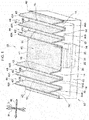
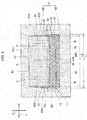
- an electronic device 10 includes a main body 12, a substrate 30, and a heat dissipating sheet 40.
- the arrow W, the arrow L, and the arrow H respectively indicate the width direction, length direction, and height direction of the electronic device 10.
- the width direction, length direction, and height direction of the electronic device 10 are referred to as the width W direction, the length L direction, and the height H direction.
- the main body 12 includes a flat cuboidal base 13, and plural protrusions 14 that project out from the base 13 toward the upper side in the height H direction.
- the main body 12 is formed by molding as described below, and is formed from resin (for example, polyamide resin), which is an example of a "first material".
- the substrate 30 is formed as a flat plate, and is disposed with its thickness direction in the height H direction.
- Packaged components that include a thermoelectric element 31 serving as an example of an "electronic component", and a communication component 32 serving as an example of a "communication section”, a packaged on the substrate 30.
- the packaged components of the substrate 30, including the thermoelectric element 31, the communication component 32, and the like, are connected together by a circuit pattern formed on the substrate 30. As illustrated in Fig. 2 , the packaged components such as the thermoelectric element 31 and the communication component 32, and the substrate 30 are encapsulated by the resin base 13 of the main body 12.
- thermoelectric element 31 A heat dissipating face of the thermoelectric element 31 is thermally connected to a connecting portion 41 of the heat dissipating sheet 40, described below, through a connecting member 33 and a heat spreader 34.
- a heat conducting member 35 is disposed at a heat absorbing face side of the thermoelectric element 31.
- the heat conducting member 35 is thermally connected to the heat absorbing face of the thermoelectric element 31.
- a portion 35A at the opposite side of the heat conducting member 35 to the thermoelectric element 31 projects out from a bottom face of the main body 12, and is exposed to the exterior.
- the heat dissipating sheet 40 is formed from a second material having higher thermal conductivity than the first material that forms the main body 12.
- the material that forms the heat dissipating sheet 40 is graphite (carbon) as an example.
- the heat dissipating sheet 40 is provided at the height H direction upper side of the main body 12 and covers the main body 12 from the height H direction upper side.
- the connecting portion 41 is formed at a width W direction central portion of the heat dissipating sheet 40 and is thermally connected to the thermoelectric element 31 described above, and an edge portion 42 is formed at both width W direction end portions of the heat dissipating sheet 40.
- the connecting portion 41 and the edge portions 42 are formed with their thickness directions in the height H direction.
- the positions (heights) of the connecting portion 41 and the edge portions 42 in the height H direction are, as an example, aligned with each other.
- the heat dissipating sheet 40 is formed with plural bent fins 43.
- the plural fins 43 are formed with their height directions in the height H direction.
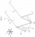
- Each of the fins 43 has a pointed shape (a shape with an isosceles triangle-shaped cross-section) that narrows in width on progression toward an apex 43A.
- the plural fins 43 are, as an example, aligned at the same height.
- the plural fins 43 formed at one side or another side of the heat dissipating sheet 40 in the width W direction are arrayed in the width W direction, and the length direction of each of the fins 43 extends in the length L direction.
- the length L direction this being the direction in which the fins 43 extend, is an example of a "direction intersecting a direction in which plural fins are arrayed".
- one fin 43 and another fin 43 are connected by a bottom portion 44A.
- Grooves 44 having V-shaped cross-sections are formed between the plural fins 43.
- the inner side of the fins 43 and the grooves 44 are each open in the length L direction, this being the length direction of each of the fins 43.
- the heat dissipating sheet 40 including the plural fins 43, the connecting portion 41, and the edge portions 42 is, for example, formed by pressing.
- a resin that forms the protrusions 14 is filled into the inner side of the fins 43, and the fins 43 are supported by the protrusions 14 from the inner side of the fins 43.
- the electronic device 10 is further provided with covering portions 16.
- the covering portions 16 are formed from the same material as the main body 12, and cover the entirety of the bottom portions 44A of the grooves 44 formed between the plural fins 43.
- Coupling portions 19 are formed between the main body 12 and the covering portions 16 during molding, described below, and the main body 12 and the covering portions 16 are integrally formed through the coupling portions 19.
- the coupling portions 19 are omitted from illustration in order to facilitate understanding of the internal structure of the electronic device 10.
- the main body 12 and the covering portions 16 are made of resin, and are integrated with the heat dissipating sheet 40 by molding.
- the covering portions 16 are formed in long thin plate shapes and are provided to the bottom portion 44A sides of the grooves 44. Portions of side face portions 43B of the fins 43 on the apex 43A sides of the fins 43 with respect to the covering portions 16 are exposed to the exterior due to the covering portions 16 being thinly formed.
- the heat dissipating component 50 includes the main body 12, the heat dissipating sheet 40, and the plural covering portions 16.
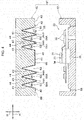
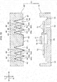
- the electronic device 10 illustrated in Fig. 1 is manufactured using a mold 51 illustrated in Fig. 3 .
- the mold 51 includes a first mold 52 and a second mold 62.
- the first mold 52 is a fixed mold
- the second mold 62 is a movable mold.
- a first cavity 53 is formed in the first mold 52 indented toward the lower side in the height H direction.
- the first cavity 53 has depth equivalent to the height of the base 13 (see Fig. 1 ).
- Injection ports 54 for injecting resin into the mold 51, and exhaust outlets 55 for removing air from the mold 51 are formed in the first mold 52.
- the injection ports 54 are open toward the inner side of plural second cavities 63 formed in the second mold 62, described below.
- Plural of the second cavities 63 are formed in the second mold 62 in a row in the width W direction, indented toward the upper side and the height H direction.
- Each of the second cavities 63 is formed to match the outer profile and size of of the plural fins 43 formed on the heat dissipating sheet 40, described above, and is formed with an inverted V-shaped cross-section.
- the heat dissipating sheet 40 is attached to the second mold 62, and the plural fins 43 are housed in the plural second cavities 63.
- Pointed portions between the plural second cavities 63 are formed as projections 64 that project out toward the first mold 52 side, and that are inserted into the grooves 44 between the plural fins 43.
- opposing faces 65, 66 that oppose the connecting portion 41 and the edge portions 42 are, as an example, aligned at the same height. As illustrated in Fig. 4 , the opposing faces 65, 66 respectively abut the connecting portion 41 and the edge portions 42 in a state in which the heat dissipating sheet 40 is attached to the second mold 62.
- the bottom portions 44A of the grooves 44 formed in the heat dissipating sheet 40 are at a lower position in the depth direction of the grooves 44 (the height H direction) than the connecting portion 41 and the edge portions 42, and gaps 68 are formed between leading end portions 64A of the projections 64 inserted into the grooves 44 and the bottom portions 44A.
- length L direction end portions 40A of the heat dissipating sheet 40 extend in a straight line along the height H direction in a state in which the heat dissipating sheet 40 is attached to the second mold 62.
- length L direction side faces 63A of the second cavities 63 are inclined with respect to the height H direction so as to approach the length L direction end sides on progression toward the height H direction lower side.
- the side faces 63A in the length L direction of the second cavities 63 have an inclination angle ⁇ with respect to the height H direction.
- the inclination angle ⁇ (taper) of the second cavities 63 is provided to facilitate removal of molded articles from the second cavities 63.
- a length L2 of the heat dissipating sheet 40 in the length L direction is shorter than a length L1 of the first cavity 53 and the second cavities 63 in the length L direction for forming the main body 12.
- the length L1 of the second cavities 63 in the length L direction is equivalent to the opening width of the second cavities 63 at the first mold 52 side and the opening width of the first cavity 53 at the second mold 62 side.
- the electronic device 10 is manufactured under the following principles using the above mold 51.
- the substrate 30, on which the thermoelectric element 31, the communication component 32, the connecting member 33, the heat spreader 34, the heat conducting member 35, and the like are mounted is housed in the first cavity 53 in the first mold 52.
- the heat dissipating sheet 40, in which the plural bent fins 43 have been formed in advance by pressing, is housed in the second cavities 63 in the second mold 62.
- the heat dissipating sheet 40 is formed in advance such that the length L2 in the length L direction is shorter than the length L1 of the first cavity 53 and the second cavities 63 in the length L direction.
- the bottom portions 44A are positioned at lower positions in the depth direction of the grooves 44 (the height H direction) than the leading end portions 64A of the projections 64 of the second mold 62 inserted into the grooves 44, and the gaps 68 are formed between the leading end portions 64A of the projections 64 and the bottom portions 44A.
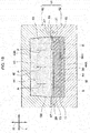
- the first mold 52 and the second mold 62 are assembled together as illustrated in Fig. 7 .
- the state in which the first mold 52 and the second mold 62 are assembled together in this manner is an example of a "set state".
- resin which is an example of a "first material"
- resin is injected in a molten state into the mold 51, toward the inner side of the fins 43 through the injection ports 54.
- the resin injected into the mold 51 flows from the inner side of the fins 43 toward the apexes 43A of the fins 43 as indicated by the arrows A in Fig. 8 , and is filled into the inner side of the fins 43.
- the fins 43 bulge and adhere to inner faces of the second cavities 63 due to the resin being filled into the inner side of the fins 43.
- through-holes that allow the resin to pass may be formed in the substrate 30 to facilitate the in-flow of the resin injected into the mold 51 toward the inner side of the fins 43.
- resin that has reached the apexes 43A of the fins 43 rebounds off the apexes 43A, and flows to end portions at both length L direction sides of the fins 43.
- the resin that has flowed to the end portions at both length direction sides of the fins 43 flows out to the outside of the fins 43 through the openings inner side the fins 43 at both length L direction sides thereof.
- the resin that has flowed out to the outside of the fins 43 passes through gaps 69 between the length L direction end portions 40A of the heat dissipating sheet 40 and the side faces 63A of the second cavities 63 and fills the gaps 68 between the leading end portions 64A of the projections 64 and the bottom portions 44A as indicated by the arrows B in Fig. 8 .
- the gaps 68 are set with appropriate dimensions for the material and temperature of the molten resin.
- the mold 51 is cooled.
- the mold 51 may be cooled naturally, or may be force cooled by cycling cold water supplied from outside through a water-cooling pipe provided to the mold 51.
- the resin that was filled into the mold 51 in the above-described manner is cooled and solidified to form the base 13, the plural protrusions 14, and the plural covering portions 16.
- the base 13 that encapsulates the thermoelectric element 31, the substrate 30, and the like is formed by the resin filled into the first cavity 53 of the first mold 52
- the protrusions 14 that support the fins 43 are formed by the resin filled into the inner side of the fins 43.
- the covering portions 16 that cover the entirety of the bottom portions 44A are formed by the resin filled into the gaps 68 between the leading end portions 64A of the projections 64 of the second mold 62 and the bottom portions 44A.
- the coupling portions 19 are formed by the resin filled into the gap 69 between the length L direction end portions 40A of the heat dissipating sheet 40 and the side faces 63A of the second cavities 63.
- the main body 12 and the covering portions 16 are integrally formed through the coupling portions 19.
- the coupling portions 19 cover the heat dissipating sheet 40 from both length L direction sides, and extend from the main body 12 toward the apexes 43A of the fins 43.
- the main body 12 and the covering portions 16 are integrated with the heat dissipating sheet 40 by molding as described above.
- the length of the main body 12 in the length L direction is similar to the length L1 of the first cavity 53 and the second cavities 63 in the length L direction.
- the length L1 of the main body 12 in the length L direction is longer than the length L2 of the heat dissipating sheet 40 in the length L direction at the portions where the coupling portions 19 are formed to the main body 12.
- the electronic device 10 manufactured using the above principles is removed from the mold 51.
- the electronic device 10 integrally includes the main body 12 that is formed from resin by molding and the sheet shaped heat dissipating sheet 40 that is provided at the main body 12, as illustrated in Fig. 1 and Fig. 2 .
- the heat dissipating sheet 40 provided at the main body 12 handles heat dissipation, rather than the main body 12, which is formed from a resin having lower thermal conductivity.
- the heat dissipating sheet 40 is sheet-shaped, and therefore needs to be continuous in order to secure heat dissipation performance.
- the bottom portions 44A of the grooves 44 are covered by the covering portions 16 in the electronic device 10 according to the first exemplary embodiment. Accordingly, even when foreign matter collected in the grooves 44 is removed using a cleaning tool such as a brush, contact between the cleaning tool and the bottom portions 44A is prevented, enabling damage to the surface of the bottom portions 44A to be suppressed. This enables reduction of the heat dissipation performance of the heat dissipating sheet 40 to be suppressed even when the heat dissipating sheet 40 is formed from, for example, a soft, easily damaged material.
- the covering portions 16 enable damage to the surface of the bottom portions 44A to be suppressed across the entirety of each bottom portion 44A since the entirety of each bottom portion 44A is covered. This enables a reduction of the heat dissipation performance of the heat dissipating sheet 40 to be more effectively suppressed.
- the covering portions 16 are provided at the bottom portion 44A sides in the grooves 44, and portions of the side face portions 43B of the fins 43 on the apex 43A sides of the fins 43 with respect to the covering portions 16 are exposed to the exterior. Accordingly, since heat in the heat dissipating sheet 40 is dissipated at the portions of the side face portions 43B of the fins 43 on the apex 43A sides of the fins 43 with respect to the covering portions 16, the heat dissipation performance of the heat dissipating sheet 40 can be secured.
- the electronic device 10 includes the sheet-shaped heat dissipating sheet 40 for heat dissipation. Accordingly, the electronic device 10 can be made more compact compared to configurations provided with a heat dissipating member such as a cast or machined article for heat dissipation.
- the main body 12 integrated with the heat dissipating sheet 40 encapsulates the thermoelectric element 31, the substrate 30, and the like, and the thermoelectric element 31, the substrate 30, and the like can therefore be protected by the main body 12.
- the surface area of the heat dissipating sheet 40 can be increased at the portions where the plural fins 43 are formed. This enables the heat dissipation performance of the heat dissipating sheet 40 to be improved.
- the protrusions 14 filled into the inner side of the fins 43 are formed in the main body 12, and the fins 43 are supported by the protrusions 14 from the inner side of the fins 43. Accordingly, the fins 43 can be suppressed from undergoing deformations such as breakage even when an external force is applied to the fins 43. This enables the heat dissipation performance of the heat dissipating sheet 40 to be maintained.
- the molding in which the thermoelectric element 31, the substrate 30, and the like are encapsulated by the main body 12, and the adhesion of the heat dissipating sheet 40 to the main body 12 are performed by the same process. Accordingly, there are fewer manufacturing processes than in cases in which the molding process in which the thermoelectric element 31, the substrate 30, and the like are encapsulated by the main body 12, and the adhesion process of the heat dissipating sheet 40 to the main body 12 are performed as separate processes. This enables the cost of the electronic device 10 to be reduced.
- the main body 12 and the covering portions 16 are integrally formed by the molding. Likewise, this enables the cost of the electronic device 10 to be reduced compared to cases in which, for example, the main body 12 and the covering portions 16 are formed separately, since there are fewer manufacturing processes.
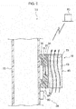
- an information processing system 70 illustrated in Fig. 9 is a system for managing temperature data of a pipe 72 having high temperature fluid flowing therein.
- the information processing system 70 includes an integrated module 80 and a server 85.
- the integrated module 80 is installed on a surface of the pipe 72, which is an example of an "installation target".
- the integrated module 80 includes the electronic device 10 described above, and a sensor 83.
- the thermoelectric element 31 of the electronic device 10 is an example of a "power supply section”
- the sensor 83 is an example of a "detector”.
- the thermoelectric element 31 is thermally connected to the pipe 72 via the heat conducting member 35.
- the sensor 83 is, for example, a thermosensor and is fixed to the surface of the pipe 72.
- the sensor 83 is connected to the substrate 30 via wiring 84.
- the temperature of the heat absorbing face of the thermoelectric element 31 thermally connected to the pipe 72 rises when the high temperature fluid flows inner side the pipe 72.
- the temperature of the heat dissipating face of the thermoelectric element 31 thermally connected to the heat dissipating sheet 40 is lowered when the fins 43 are exposed to, for example, external air such as an air current 73.
- Packaged components including the communication component 32 and the like, packaged on the substrate 30, and the sensor 83, operate using power generated by the thermoelectric element 31.
- the sensor 83 outputs signals in accordance with the surface temperature of the pipe 72, and the communication component 32 transmits the data detected by the sensor 83 to the server 85.
- the server 85 receives and accumulates data transmitted from the integrated module 80. Note that an operation lamp indicating the operational state of the communication component 32 or the like may be provided to the integrated module 80.
- the surroundings of the pipe 72 reach a high temperature due to heat emitted by the pipe 72, and data can be transmitted from the integrated module 80 even in environments ill-suited to human entry, such as those with high levels of dust and grime. This enables the temperature state of the pipe 72 to be ascertained based on the data transmitted from the integrated module 80.
- the electronic device 10 is formed as a sensor node-type integrated module combined with a sensor in the first exemplary embodiment, the electronic device 10 may be employed in applications other than that described above.
- thermoelectric element 31 As an example of an "electronic component", electronic components other than the thermoelectric element 31 may be included.
- the main body 12 is formed using polyamide resin as an example of a "first material"
- the main body 12 may be formed from a resin other than polyamide resin.
- the heat dissipating sheet 40 is formed using graphite as an example of a "second material", as long as this material has higher thermal conductivity than the material forming the main body 12, the heat dissipating sheet 40 may be formed from, for example, a metal such as aluminum or copper, or may be formed from a material other than a metal.
- the covering portions 16 cover the entirety of the bottom portions 44A
- the covering portions 16 may be configured with a size and shape that covers a portion of the bottom portions 44A.
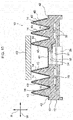
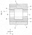
- a placement member 49 is disposed at the opposite side of the heat dissipating sheet 40 to the main body 12 (the upper side). Since foreign matter does not easily build up below the placement member 49, covering portions 16 are omitted below the placement member 49. Namely, the covering portions 16 are positioned at the outsides of the placement member 49 when the heat dissipating sheet 40 and the disposing member 49 are viewed along the height direction of the fins 43.
- the exposed surface area of the heat dissipating sheet 40 increases by an amount corresponding to the portions where the covering portions 16 are not provided below the placement member 49, enabling the heat dissipation performance of the heat dissipating sheet 40 to be improved.
- each of the fins 43 has a pointed shape (an isosceles triangle-shaped cross-section) that narrows in width on progression toward the apexes 43A in the first exemplary embodiment
- the fins 43 may have another cross-section profile, such as a rectangle-shaped cross-section.
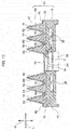
- the electronic device 10 includes the thermoelectric element 31, the connecting member 33, the heat spreader 34, the heat conducting member 35, the substrate 30, and the heat dissipating component 50 integrated together in the first exemplary embodiment, the heat dissipating component 50 may be independent from the device body of the electronic device 10.
- a device body 11 is formed by the thermoelectric element 31, the connecting member 33, the heat spreader 34, the heat conducting member 35, the substrate 30, and an encapsulating resin 25 that encapsulates these components.
- the heat dissipating component 50 includes the main body 12, the heat dissipating sheet 40, and the plural covering portions 16, and is formed independently from the device body 11.
- the heat dissipating component 50 is a molded article, and the heat dissipating component 50 can be provided at low cost, enabling the cost of the electronic device 10 to be reduced.
- the electronic device 10 may include a battery that stores power generated by the thermoelectric element 31.
- the thermoelectric element 31 and the battery correspond to an example of a "power supply section”.
- the sensor 83 and the communication component 32 may operate using power from at least one out of the thermoelectric element 31 or the battery.
- the information processing system 70 may be employed in applications other than the management of temperature data of the pipe 72 having high temperature fluid flowing therein.
- the manufacturing method differs as follows from the manufacturing method for an electronic device according to the first exemplary embodiment described above.
- the electronic device is manufactured under the following principles.
- the substrate 30 is housed in the first cavity 53 inner side the first mold 52, and the heat dissipating sheet 40 is housed in the second cavities 63 inner side the second mold 62.
- the heat dissipating sheet 40 is pre-formed so as to have a length along the length L direction that is equal to the length L1 of the first cavity 53 and the second cavities 63 in the length L direction.
- the length L direction end portions 40A of the heat dissipating sheet 40 are inclined with respect to the height H direction so as to approach the length L direction end sides on progression toward the height H direction lower side. Then, in a state in which the heat dissipating sheet 40 is attached to the second mold 62, the length L direction end portions 40A of the heat dissipating sheet 40 extend in a straight line along the side faces 63A in the length L direction of the second cavities 63.
- the bottom portions 44A are formed in flat shapes, and are positioned at lower positions than the lower face of the second mold 62.
- cut-outs 47 also see Fig. 14 , which are examples of an "inflow port" are pre-formed in both length direction side end portions of the bottom portions 44A of the heat dissipating sheet 40.
- the cut-outs 47 are formed when the heat dissipating sheet 40 is pressed.
- the cut-outs 47 penetrate through the thickness direction of the bottom portions 44A, and place the inner side of the fins 43 in communication with the grooves 44.
- the cut-outs 47 are cut out in a circular arc shape as an example.
- the bottom portions 44A are positioned at a lower position in the depth direction of the grooves 44 (the height H direction) than the leading end portions 64A of the projections 64 of the second mold 62 inserted into the grooves 44, and the gaps 68 are formed between the leading end portions 64A of the projections 64 and the bottom portions 44A. Then, in a state in which the heat dissipating sheet 40 and the substrate 30 are thus set up in the mold 51, the first mold 52 and the second mold 62 are assembled together.
- resin which is an example of a "first material"
- the resin injected into the mold 51 flows from the inner side of the fins 43 toward the apexes 43A of the fins 43 as indicated by the arrows A in Fig. 16 , and is filled into the inner side of the fins 43.
- the fins 43 bulge and adhere to the inner faces of the second cavities 63 due to the resin being filled into the inner side of the fins 43.
- Resin that has reached the apexes 43A of the fins 43 rebounds off the apexes 43A and flows to the end portions inner side the fins 43 at both length L direction sides thereof.
- the resin that has flowed to the end portions inner side the fins 43 at both length L direction sides thereof passes through the cut-outs 47 and fills the gaps 68 between the leading end portions 64A of the projections 64 and the bottom portions 44A as indicated by the arrows B in Fig. 16 .
- an electronic device 100 (see Fig. 16 ) is manufactured under the principles above.
- the main body 12 and the covering portions 16 are formed integrally through coupling portions 20 formed in the cut-outs 47.
- the main body 12 and the covering portions 16 are integrated with the heat dissipating sheet 40 by molding as described above.
- the coupling portions 19 (see Fig. 8 ) are not formed.
- the main body 12 and the covering portions 16 are integrally formed by molding similarly to in the first exemplary embodiment. Accordingly, there are fewer manufacturing processes than in cases in which, for example, the main body 12 and the covering portions 16 are formed separately. This enables the cost of the electronic device 10 to be reduced.
- the length L direction end portions 40A are inclined with respect to the height H direction so as to approach the length L direction end sides on progression toward the height H direction lower side. Accordingly, the surface area of the side face portions of the heat dissipating sheet 40 increases by an amount corresponding to the inclined portions, enabling the heat dissipation performance of the heat dissipating sheet 40 to be improved.
- cut-outs 47 of the heat dissipating sheet 40 are cut out in circular arc shapes in the second exemplary embodiment, a shape other than a circular arc may be cut out.
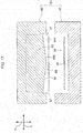
- the projections 64 of the second mold 62 may be formed as follows.
- the projections 64 of the second mold 62 are formed such that the end portions at both length L direction sides thereof have a shorter projection length than that of length L direction central portions thereof.
- the gaps 68 formed between the leading end portions 64A of the projections 64 and the bottom portions 44A can be made larger at both length L direction sides than at the length L direction central portion. This enables a smooth flow of resin passing through the cut-outs 47 and filling the gaps 68 between the leading end portions 64A of the projections 64 of the second mold 62 and the bottom portions 44A.
- the manufacturing method differs from the manufacturing method for an electronic device according to the second exemplary embodiment, described above, as follows.
- the second mold 62 is structured as follows.
- the projections 64 of the second mold 62 are formed such that the length L direction central portions thereof have a shorter projection length that that of the end portions at both length L direction sides thereof.
- the leading end portions 64A of the projections 64 are formed so as to approach the bottom portions 44A on progression from the length L direction central portions thereof toward the end portions.
- the electronic device is manufactured under the following principles using a second mold 62 with such a structure.
- the substrate 30 is housed in the first cavity 53 inner side the first mold 52, and the heat dissipating sheet 40 is housed in the second cavities 63 inner side the second mold 62.
- the heat dissipating sheet 40 is pre-formed so as to have a length in the length L direction that is equal to the length L1 of the first cavity 53 and the second cavities 63 in the length L direction.
- the length L direction end portions 40A of the heat dissipating sheet 40 are inclined with respect to the height H direction so as to approach the length L direction end sides on progression toward the height H direction lower side. Then, in a state in which the heat dissipating sheet 40 is attached to the second mold 62, the length L direction end portions 40A of the heat dissipating sheet 40 extend in a straight line along the side faces 63A of the second cavities 63 in the length L direction.
- the bottom portions 44A are formed in flat shapes, and are positioned at the same height as the lower face of the second mold 62.
- Holes 48 which are examples of an "inflow port", are pre-formed in length direction central portions of the bottom portions 44A of the heat dissipating sheet 40.
- the holes 48 are formed when the heat dissipating sheet 40 is pressed.
- the holes 48 penetrate the thickness direction of the bottom portions 44A and place the inner side of the fins 43 in communication with the grooves 44.
- the holes 48 are formed in a circular shape as an example.
- the gaps 68 are formed between the leading end portions 64A of the projections 64 of the second mold 62 inserted into the grooves 44 and the bottom portions 44A. Then, in a state in which the heat dissipating sheet 40 and the substrate 30 are thus set up in the mold 51, the first mold 52 and the second mold 62 are assembled together.
- resin which is an example of a "first material"
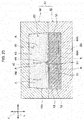
- the resin injected into the mold 51 flows from the inner side of the fins 43 toward the apexes 43A of the fins 43 as indicated by the arrows A in Fig. 20 , and is filled into the inner side of the fins 43.
- the fins 43 bulge and adhere to the inner faces of the second cavities 63 due to resin being filled into the inner side of the fins 43.
- the resin inner side the fins 43 passes through the holes 48 and fills the gaps 68 between the leading end portions 64A of the projections 64 and the bottom portions 44A, as indicated by the arrows B in Fig. 20 .
- the resin filled into the mold 51 as described above is cooled and solidified to form the base 13, the plural protrusions 14, and the plural covering portions 16 (see Fig. 1 , Fig. 2 ), similarly to in the first and second exemplary embodiments.
- an electronic device 110 (also see Fig. 21 , Fig. 22 ) is manufactured by the principles described above.
- the main body 12 and the covering portions 16 are integrally formed through coupling portions 21 formed in the holes 48 (also see Fig. 22 ).
- the main body 12 and the covering portions 16 are integrated with the heat dissipating sheet 40 by molding as described above.
- the covering portions 16 are formed such that the thickness of the length L direction central portions of the covering portions 16 is thicker than the thickness of both length L direction end portions of the covering portions 16.
- the main body 12 and the covering portions 16 are integrally formed by molding similarly to in the first and second exemplary embodiment. Accordingly, there are fewer manufacturing processes than in cases in which, for example, the main body 12 and the covering portions 16 are formed separately. This enables the cost of the electronic device 10 to be reduced.
- the covering portions 16 are formed such that the thickness of the length L direction central portions of the covering portions 16 is thicker than the thickness of both length L direction side end portions of the covering portions 16. Accordingly, in cases in which, for example, the electronic device 110 is employed outdoors with the fins 43 facing upward, foreign matter collected on the covering portions 16 can be washed off by rainfall due to the incline (taper) of the covering portions 16.
- the holes 48 of the heat dissipating sheet 40 are formed circular shapes in the third exemplary embodiment, the holes 48 may be formed in a shape other than a circle.
- the manufacturing method differs from the manufacturing method for an electronic device according to the first to the third exemplary embodiments, described above, as follows.
- the mold 51 is structured as follows. Out of the inner faces (molding faces) of the first cavity 53 formed in the first mold 52, the side faces of the first cavity 53 that oppose the side faces of the main body 12 and the bottom faces of the first cavity 53 that oppose the bottom faces of the main body 12, are each formed with a transfer portion 56. Similarly, out of the inner faces (molding faces) of the second cavities 63 formed in the second mold 62, leading end faces of the projections 64 that oppose the surface of the covering portions 16 are formed with a transfer portion 57.
- the respective transfer portions 56, 57 are structured to include indentations and protrusions so as to be able to form graining 22 on the surfaces of the main body 12 and the covering portions 16 of an electronic device 120 as described below.
- the electronic device 120 is manufactured under similar principles to those of the first exemplary embodiment described above, using the mold 51 that includes such transfer portions 56, 57.
- graining 22 is respectively formed on the side faces of the main body 12, the bottom faces of the main body 12, and the surface of the covering portions 16 as an example of "anti-fouling treatment", using the transfer portions 56, 57.
- the graining 22 includes plural protrusions 22A (land portions). A shape that exhibits the advantageous effects of not being easily damaged, not easily becoming dirty, and being easily cleaned is suitably applied for the graining 22.
- the side faces of the main body 12, the bottom faces of the main body 12, and the surface of the covering portions 16 are formed with the graining 22. Due to the graining 22, this thereby enables the side faces of the main body 12, the bottom faces of the main body 12, and the surface of the covering portions 16 to be suppressed from becoming dirty.
- a fine periodic structure 23 may be formed on the side faces of the main body 12, the bottom faces of the main body 12, and the surface plural covering portions 16, instead of the graining 22 described above (see Fig. 23 , Fig. 24 ).
- the fine periodic structure 23 is formed by changing the structure of the transfer portions 56, 57 of the mold 51 (see Fig. 23 ). As illustrated in Fig. 26 , as an example, the fine periodic structure 23 includes plural fine projections 23A that form a lattice.
- the array pitch of the plural fine projections is preferably from 5 ⁇ m to 20 ⁇ m.
- a shape that exhibits water repellency due to the lotus effect, or a shape that exhibits self-cleaning activity is suitably applied as the fine periodic structure 23.
- a fine periodic structure 23 having such plural fine projections also enables the side faces of the main body 12, the bottom faces of the main body 12, and the surface of the covering portions 16 to be suppressed from becoming dirty.
- the graining 22 or the fine periodic structure 23 is formed by the transfer portions 56, 57 in the fourth exemplary embodiment, the graining 22 or the fine periodic structure 23 may be formed by an additional process after removing the electronic device 120 from the mold 51.
- a coating layer 24 having hydrophilicity and hydrophobicity may be formed on the side faces of the main body 12, the bottom faces of the main body 12, and the surface of the covering portions 16,.
- a coating material having hydrophilicity and hydrophobicity examples include a combination of an acrylic polymer having hydrophilicity and a fluorine polymer having hydrophobicity, or fine particles of a hydrophobic fluorine resin dispersed in a hydrophilic coating material at intervals smaller than dirt particles.
- Such a coating layer 24 also enables the side faces of the main body 12, the bottom faces of the main body 12, and the surface of the covering portions 16 to be suppressed from becoming dirty.
- the graining 22, the fine periodic structure 23, and the coating layer 24 may be formed on the side faces of the main body 12 and the bottom faces of the main body 12 without being formed on the surface of the covering portions 16.
- the graining 22, the fine periodic structure 23, and the coating layer 24 may be formed on the surface of the covering portions 16 without being formed on the side faces of the main body 12 or the bottom faces of the main body 12.
- the graining 22, the fine periodic structure 23, and the coating layer 24 may be formed anywhere, as long as they are formed on at least a portion of a surface of the main body 12 or the covering portions 16, or both.
- an integrated module 160 includes a power generating module 161, a power storing module 162, a sensor 163, a controller 164, a memory 165, a communication circuit 166, and an antenna 167.
- the electronic device of the first to the fourth exemplary embodiment described above is employed in the power generating module 161.
- the power generating module 161 includes the substrate 30 packaged with the thermoelectric element 31 and the like (not including the communication component 32), the main body 12, the heat dissipating sheet 40, and the plural covering portions 16 (see Fig. 1 to Fig. 27 , mentioned above).
- the power storing module 162 is connected to the power generating module 161, and stores power generated by the power generating module 161. Any component with functionality for storing power may be employed as the power storing module 162.
- the power storing module 162 is preferably, for example, a solid-state secondary battery, from the viewpoints of having high safety while saving space.
- the power generating module 161 and the power storing module 162 form a power supply section 168. Power is supplied to the sensor 163, the controller 164, and the communication circuit 166 from at least one out the power generating module 161 and the power storing module 162 that form the power supply section 168.
- the power storing module 162 may be omitted in cases in which power can be supplied stably from the power generating module 161.
- the sensor 163 is an example of a "detector".
- a sensor that detects temperature, humidity, pressure, light, sound, magnetic waves, acceleration, vibration, gas, fine particles, or the like may be employed as the sensor 163.
- a distance sensor that measures a distance to a target object by emitting infrared light toward the target object and receiving light reflected back from the target object
- a weight sensor that measures the weight of a target object
- a water level sensor that detects data such a water level, or the like may be employed as the sensor 163.
- the controller 164 transmits various data detected by the sensor 163 to a server via the communication circuit 166 and the antenna 167.
- the controller 164 may, for example, transmit secondary data based on the various data detected by the sensor 163 and other data to the server.
- the controller 164 may compute secondary data by performing a specific calculation using the various data detected by the sensor 163, and transmit the secondary data to the server.
- the memory 165 stores the various data detected by the sensor 163 and computed secondary data on instruction by the controller 164. Stored information is read on instruction from the controller 164.
- the communication circuit 166 and the antenna 167 form a communication section 169.
- the communication section 169 transmits and receives data between the controller 164 and the server, which is not illustrated in the drawings.
- wireless communication using the antenna 167 is employed as illustrated in the example of Fig. 28 , wired communication may be employed instead of wireless communication.
- the integrated module 160 described above employs, for example, an information processing system 170 according to the fifth exemplary embodiment.
- the information processing system 170 includes plural integrated modules 160 and a server 175.
- the plural integrated modules 160 are installed in manholes 176.
- the plural integrated modules 160 installed in plural manholes 176 are connected to the server 175 via a network 177.
- data may be transmitted from the integrated modules 160 to the server 175 by near field communication each time a travelling vehicle provided with the server 175 approaches the integrated modules 160 installed in each of the manholes 176.
- An integrated module 160 may be installed anywhere on a structural member of a manhole 176.
- Each integrated module 160 is, for example, fixed to a lid 178 or a concrete pipe 179, which are structural members of the manholes 176, depending on the detection target of the sensor 163 and the type of the sensor 163.
- the thermoelectric element 31 provided to each integrated module 160 is thermally connected to the structural member of a manhole 176, which is an example of an "installation target", and power is generated due to a temperature difference between the structural member of the manhole 176 and either external air or the temperature inner side the manhole 176.
- the information processing system 170 is employed in order to ascertain degradation of the structural members of manholes 176 (the lids 178 or the concrete pipes 179).
- a sensor 163 detects the temperature or humidity inner side a manhole 176, vibrations (acceleration) acting on the structural member of the manhole 176, or the like, and data detected by the sensor 163 is accumulated in the memory 165.
- the controller 164 transmits the data accumulated by the memory 165 via the communication circuit 166 and the antenna 167.
- the server 175 provided to the measuring vehicle 180 collects the data.
- the server 175 combines position information of the vehicle 180 from a global positioning system (GPS) with the collected data, and displays the collected data on a map displayed on an in-car monitor.
- GPS global positioning system
- the degree of degradation of the concrete pipe 179 in each of the manholes 176 is estimated from the information expressing the temperature, humidity, vibrations, or the like.
- a camera 182 that acquires images of the lid 178 of the manhole 176 is attached to a lower portion of the measuring vehicle 180, and degradation of the lid 178 (an iron part) of the manhole 176 is determined using image recognition. Based on the result, the time to replace the lid 178 of the manhole 176 may be sold as information to a local government. Rather than a specialized measuring vehicle, the vehicle collecting the data may, for example, be a garbage truck operated by the local government. Installing the receiving device 181 and the camera 182 to the bottom portion of a garbage truck enables data to be collected periodically without incurring collection expenses.
- the sensor 163 may detect the concentration of a gas generated inner side the manhole 176.
- the gas generated inner side the manhole 176 may, for example, be hydrogen sulfide gas.
- Hydrogen sulfide gas generated by a sewer 183 is known to rapidly degrade structural members of manholes 176.
- the generation of hydrogen sulfide gas is also a cause of complaint among local residents.
- Using a hydrogen sulfide gas sensor as the sensor 163 increases the precision of degradation predictions for the structural members of manholes 176, and enables complaints by residents to be swiftly dealt with.
- the senor 163 it is sufficient for the sensor 163 to detect at least one out of the temperature, humidity, or vibrations inner side a manhole 176, or a concentration of gas generated inner side the manhole 176.
- the information processing system 170 is applied in order to predict a flow rate in the sewer 183 connected to the manholes 176.
- the sensor 163 employs, for example, a water level meter or a flow meter. Installing the sensor 163, which is a water level meter or a flow meter, in the manholes 176 enables the flow rate in the sewer 183 to be ascertained in fine detail.
- the sensor 163 is incorporated into the integrated module 160 in Fig. 31 , for example, a sensor controller that controls the operation of an external sensor may be provided instead of the sensor 163.
- the sensor controller may control a sensor such as a water level meter or a flow meter, not illustrated in the drawings, disposed in the sewer 183, and may acquire information detected by the sensor. Moreover, information detected by the sensor may be transmitted to the sensor controller wirelessly.
- a sensor such as a water level meter or a flow meter, not illustrated in the drawings, disposed in the sewer 183.
- the flow rate in the sewer 183 is detected by the sensor 163 once every day, or once every hour, and data detected by the sensor 163 travels along a high speed communication line and is gathered in the server 175 of a data center 184.
- the flow rate data of the sewer 183 detected by the sensor 163 may be transmitted at the same time that measurement is made, or may be accumulated and then transmitted every day or week in order to reduce power consumption.
- data may be collected by a measuring vehicle similarly to in the first application example.
- a relationship can be established between weather phenomena and the flow rate in the sewer 183 from the results of analysis of flow rate data in the sewer 183 and rainfall data from a meteorological agency. Then, the flow rate in the sewer 183 at each location may be predicted from the rainfall data of the meteorological agency, and charges made for the provision and distribution of the prediction data.
- An information processing system 170 capable of continuously updating data is useful since flow rates in the sewer 183 may change from year to year according to residential home construction, residential statuses, and land development status.
- the information processing system 170 can also be utilized for flow rate measurements in the sewer 183 in cases of locally concentrated heavy rainfall.
- minute-by-minute measurement and information transmission of water levels in the sewer 183 are needed to secure worker safety in the sewer 183 and to prevent the sewer 183 from flooding.
- data gathering may be limited to a small number of integrated modules 160 installed in manholes 176 at relatively low elevations.
- the power storing module 162 of the integrated module 160 that measures the water level is preferably stored with sufficient power in advance.
- the controller 164 sequentially transmits data to the server 175 through the communication circuit 166 and a high speed communication line.
- the server 175 can issue the received data as a warning to the smartphones and tablets of workers and residents near the flooding.
- data may be collected in a server provided to a measuring vehicle parked over a specific manhole 176, using near field communication.
- the information processing system 170 is employed for the security and operation history of the manholes 176.
- the sensor 163 detects opening and closing of the lids 178 of the manholes 176.
- the sensor 163, for example, employs an acceleration sensor or an opening and closing switch. It is sufficient for the sensor 163 to detect at least one out of acceleration of the lid 178 of the manhole 176 or open and closed states of the lid 178 of the manhole 176 in order to detect opening and closing of the lid 178 of the manhole 176.
- Data (signals) output from the sensor 163 in accordance with the opening and closing of the lid 178 of the manhole 176 are received by the server 175.
- security countermeasures for example, terrorist bombing countermeasures
- the operation history of cleaning operations of the sewer 183 can be confirmed.
- the information processing system 170 is employed for acquiring road traffic information.
- the sensor 163 detects vehicles 185, 186, 187 passing over the manhole 176.
- an acceleration sensor, a magnetic sensor, a microphone, or the like may be employed by the sensor 163.
- Signals obtained from the sensor 163 depend on the number vehicles that pass over the manhole 176.
- Data (signals) output from the sensor 163 are received by the server 175.
- traffic information can be obtained even for small roads, alley ways, and the like for which measurements are not made using current road traffic information communication systems. This enables finely detailed traffic information to be provided.
- the type of the vehicle 185, 186, 187 (for example, small car, regular car, truck, etc.) passing over the manhole 176 may be detected from the magnitude of the detection value of the sensor 163.
- a data set associating the detection value of the sensor 163 with the type of the vehicle may be pre-stored in the memory 165.
- Information indicating the type of vehicle determined from the detection value of the sensor 163 and the data set described above is transmitted from the controller 164 to the server 175. This enables the type of vehicle passing over the manhole 176 to be ascertained.
- individual identification information of the vehicle 185, 186, 187 passing over the manhole 176 may be detected by the sensor 163.
- the sensor 163 For example, in cases in which a magnetic sensor is employed as the sensor 163, it is possible that the characteristics of the vehicle could be obtained from the response of the magnetic sensor. Namely, individual vehicles can be recognized by, for example, installing a medium that gives out characteristic magnetism by vehicle. Analysis of differences in the flow of vehicles in a city by vehicle type is relevant to municipal road control and municipal evaluation, such as for schemes to guide certain vehicles onto certain roads.
- the senor 163 it is sufficient for the sensor 163 to detect at least one out of the number, type, or individual identification information of vehicles passing over the manhole 176.
- the information processing system 170 is employed for measuring amounts of rainfall.
- an X-band radar for predicting weather is employed as the sensor 163.
- Radio waves from X-band radar do not reach beyond an area where rain is falling during heavy rains, and will not cross over large objects such as mountains.
- there are many issues in current radars regarding detection and tracking of areas where heavy rain suddenly or rapidly begins to fall. Highly precise prediction demands high temporal and spatial resolution.
- a dedicated server 175 is employed in the first to the fifth example applications described above, a regular computer may be employed as the server 175.
- a program that executes operations performed by the controller 164 and the server 175 may be installed and executed in a regular computer that functions as the server 175. In such cases, the program may be supplied using a recording medium or may be downloaded over a network.
Landscapes
- Physics & Mathematics (AREA)
- General Physics & Mathematics (AREA)
- Engineering & Computer Science (AREA)
- Microelectronics & Electronic Packaging (AREA)
- Thermal Sciences (AREA)
- Cooling Or The Like Of Semiconductors Or Solid State Devices (AREA)
- Cooling Or The Like Of Electrical Apparatus (AREA)
- Chemical & Material Sciences (AREA)
- Materials Engineering (AREA)
Abstract
Description
- Technology disclosed herein relates to a heat dissipating component, a manufacturing method for a heat dissipating component, an electronic device, a manufacturing method for an electronic device, an integrated module, and an information processing system.
- In an electronic device provided with an electronic component that requires heat dissipation, sometimes a heat dissipating component thermally connected to the electronic component is employed to dissipate heat.
-
- Japanese Patent Application Laid-Open (
JP-A) No. H07-7110 -
JP-A No. H05-326762 -
JP-A No. 2009-152537 - In an electronic device provided with an heat dissipating component like that described above, there is a desire to be able to suppress lowering in heat dissipation performance of the heat dissipating component.
- An object of one aspect of technology disclosed herein is to suppress reduction of the heat dissipation performance of a heat dissipating component.
- According to an aspect of the embodiments, a heat dissipating component includes: a main body formed from a first material; a heat dissipating sheet that is formed from a second material having higher thermal conductivity than the first material, that is provided at the main body, and that includes plural fins thermally connected to each other at positions other than apexes and a connecting portion thermally connecting the plural fins to an electronic component; and a covering portion that is formed from the first material, and that covers at least a portion of a bottom portion of a groove between the plural fins.
-
-
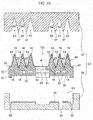
Fig. 1 is a perspective view of an electronic device according to a first exemplary embodiment. -
Fig. 2 is a cross-section as viewed from the front of an electronic device according to the first exemplary embodiment. -
Fig. 3 is a diagram for explaining a manufacturing method for an electronic device according to the first exemplary embodiment. -
Fig. 4 is a diagram for explaining a manufacturing method for an electronic device according to the first exemplary embodiment. -
Fig. 5 is a diagram for explaining a manufacturing method for an electronic device according to the first exemplary embodiment. -
Fig. 6 is a partial enlarged perspective view of a heat dissipating sheet according to the first exemplary embodiment. -
Fig. 7 is a diagram for explaining a manufacturing method for an electronic device according to the first exemplary embodiment. -
Fig. 8 is a diagram for explaining a manufacturing method for an electronic device according to the first exemplary embodiment. -
Fig. 9 is a diagram illustrating an information processing system according to the first exemplary embodiment. -
Fig. 10 is a cross-section as viewed from the front illustrating a first modified example of an electronic device according to the first exemplary embodiment. -
Fig. 11 is a plan view illustrating a first modified example of an electronic device according to the first exemplary embodiment. -
Fig. 12 is a cross-section as viewed from the front illustrating a second modified example of an electronic device according to the first exemplary embodiment. -
Fig. 13 is a diagram for explaining a manufacturing method of an electronic device according to a second exemplary embodiment. -
Fig. 14 is a diagram for explaining a manufacturing method of an electronic device according to the second exemplary embodiment. -
Fig. 15 is a partial enlarged perspective view of a heat dissipating sheet according to the second exemplary embodiment. -
Fig. 16 is a diagram for explaining a manufacturing method of an electronic device according to the second exemplary embodiment. -
Fig. 17 is a diagram for explaining a modified example of a manufacturing method for an electronic device according to the second exemplary embodiment. -
Fig. 18 is a side face cross-section of a first mold for manufacturing an electronic device according to a third exemplary embodiment. -
Fig. 19 is a diagram for explaining a manufacturing method of an electronic device according to the third exemplary embodiment. -
Fig. 20 is a diagram for explaining a manufacturing method for an electronic device according to the third exemplary embodiment. -
Fig. 21 is a cross-section as viewed from the front of an electronic device according to the third exemplary embodiment. -
Fig. 22 is a side face cross-section of an electronic device according to the third exemplary embodiment. -
Fig. 23 is a diagram for explaining a manufacturing method of an electronic device according to a fourth exemplary embodiment. -
Fig. 24 is an enlarged view of graining formed on an electronic device according to the fourth exemplary embodiment. -
Fig. 25 is a cross-section as viewed from the front illustrating a first modified example of an electronic device according to a fourth exemplary embodiment. -
Fig. 26 is an enlarged view of a fine periodic structure in a first modified example of an electronic device according to the fourth exemplary embodiment. -
Fig. 27 is a cross-section as viewed from the front illustrating a second modified example of an electronic device according to the fourth exemplary embodiment. -
Fig. 28 is a diagram illustrating an integrated module according to a fifth exemplary embodiment. -
Fig. 29 is a diagram illustrating an information processing system according to the fifth exemplary embodiment. -
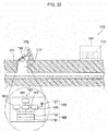
Fig. 30 is a diagram illustrating a usage state of an information processing system according to a first example application of the fifth exemplary embodiment. -
Fig. 31 is a diagram illustrating a usage state of an information processing system according to a second example application of the fifth exemplary embodiment. -
Fig. 32 is a diagram illustrating a usage state of an information processing system according to a third example application of the fifth exemplary embodiment. -
Fig. 33 is a diagram illustrating a usage state of an information processing system according to a fourth example application of the fifth exemplary embodiment. -
Fig. 34 is a diagram illustrating a usage state of an information processing system according to a fifth example application of the fifth exemplary embodiment. - Explanation follows regarding a first exemplary embodiment of technology disclosed herein.
- As illustrated in
Fig. 1 andFig. 2 , anelectronic device 10 according to the first exemplary embodiment includes amain body 12, asubstrate 30, and aheat dissipating sheet 40. - In each of the drawings, the arrow W, the arrow L, and the arrow H respectively indicate the width direction, length direction, and height direction of the
electronic device 10. The width direction, length direction, and height direction of theelectronic device 10 are referred to as the width W direction, the length L direction, and the height H direction. - The
main body 12 includes aflat cuboidal base 13, andplural protrusions 14 that project out from thebase 13 toward the upper side in the height H direction. Themain body 12 is formed by molding as described below, and is formed from resin (for example, polyamide resin), which is an example of a "first material". - The
substrate 30 is formed as a flat plate, and is disposed with its thickness direction in the height H direction. Packaged components that include athermoelectric element 31 serving as an example of an "electronic component", and acommunication component 32 serving as an example of a "communication section", a packaged on thesubstrate 30. The packaged components of thesubstrate 30, including thethermoelectric element 31, thecommunication component 32, and the like, are connected together by a circuit pattern formed on thesubstrate 30. As illustrated inFig. 2 , the packaged components such as thethermoelectric element 31 and thecommunication component 32, and thesubstrate 30 are encapsulated by theresin base 13 of themain body 12. - A heat dissipating face of the
thermoelectric element 31 is thermally connected to a connectingportion 41 of theheat dissipating sheet 40, described below, through a connectingmember 33 and aheat spreader 34. Aheat conducting member 35 is disposed at a heat absorbing face side of thethermoelectric element 31. Theheat conducting member 35 is thermally connected to the heat absorbing face of thethermoelectric element 31. Aportion 35A at the opposite side of theheat conducting member 35 to thethermoelectric element 31 projects out from a bottom face of themain body 12, and is exposed to the exterior. - The
heat dissipating sheet 40 is formed from a second material having higher thermal conductivity than the first material that forms themain body 12. In the first exemplary embodiment, the material that forms theheat dissipating sheet 40 is graphite (carbon) as an example. Theheat dissipating sheet 40 is provided at the height H direction upper side of themain body 12 and covers themain body 12 from the height H direction upper side. - The connecting
portion 41 is formed at a width W direction central portion of theheat dissipating sheet 40 and is thermally connected to thethermoelectric element 31 described above, and anedge portion 42 is formed at both width W direction end portions of theheat dissipating sheet 40. The connectingportion 41 and theedge portions 42 are formed with their thickness directions in the height H direction. The positions (heights) of the connectingportion 41 and theedge portions 42 in the height H direction are, as an example, aligned with each other. - At both sides of the connecting
portion 41, theheat dissipating sheet 40 is formed with pluralbent fins 43. Theplural fins 43 are formed with their height directions in the height H direction. Each of thefins 43 has a pointed shape (a shape with an isosceles triangle-shaped cross-section) that narrows in width on progression toward an apex 43A. Theplural fins 43 are, as an example, aligned at the same height. - As illustrated in
Fig. 1 , theplural fins 43 formed at one side or another side of theheat dissipating sheet 40 in the width W direction are arrayed in the width W direction, and the length direction of each of thefins 43 extends in the length L direction. The length L direction, this being the direction in which thefins 43 extend, is an example of a "direction intersecting a direction in which plural fins are arrayed". As an example of being thermally connected at positions other than apexes, onefin 43 and anotherfin 43 are connected by abottom portion 44A. -
Grooves 44 having V-shaped cross-sections are formed between theplural fins 43. The inner side of thefins 43 and thegrooves 44 are each open in the length L direction, this being the length direction of each of thefins 43. Theheat dissipating sheet 40 including theplural fins 43, the connectingportion 41, and theedge portions 42 is, for example, formed by pressing. A resin that forms theprotrusions 14 is filled into the inner side of thefins 43, and thefins 43 are supported by theprotrusions 14 from the inner side of thefins 43. - The
electronic device 10 is further provided with coveringportions 16. The coveringportions 16 are formed from the same material as themain body 12, and cover the entirety of thebottom portions 44A of thegrooves 44 formed between theplural fins 43. Coupling portions 19 (seeFig. 8 ) are formed between themain body 12 and the coveringportions 16 during molding, described below, and themain body 12 and the coveringportions 16 are integrally formed through thecoupling portions 19. InFig. 1 , the coupling portions 19 (seeFig. 8 ) are omitted from illustration in order to facilitate understanding of the internal structure of theelectronic device 10. - The
main body 12 and the coveringportions 16 are made of resin, and are integrated with theheat dissipating sheet 40 by molding. The coveringportions 16 are formed in long thin plate shapes and are provided to thebottom portion 44A sides of thegrooves 44. Portions ofside face portions 43B of thefins 43 on the apex 43A sides of thefins 43 with respect to the coveringportions 16 are exposed to the exterior due to the coveringportions 16 being thinly formed. - In the
electronic device 10 according to the first exemplary embodiment, a structure that remains after thethermoelectric element 31, the connectingmember 33, theheat spreader 34, theheat conducting member 35, and thesubstrate 30 have been removed from theelectronic device 10 forms aheat dissipating component 50. Namely, theheat dissipating component 50 includes themain body 12, theheat dissipating sheet 40, and theplural covering portions 16. - Next, explanation follows regarding a manufacturing method for the
electronic device 10 including theheat dissipating component 50 according to the first exemplary embodiment. - The
electronic device 10 illustrated inFig. 1 , as an example, is manufactured using amold 51 illustrated inFig. 3 . Themold 51 includes afirst mold 52 and asecond mold 62. As an example, thefirst mold 52 is a fixed mold, and thesecond mold 62 is a movable mold. - A
first cavity 53 is formed in thefirst mold 52 indented toward the lower side in the height H direction. Thefirst cavity 53 has depth equivalent to the height of the base 13 (seeFig. 1 ). Thesubstrate 30, onto which thethermoelectric element 31, thecommunication component 32, the connectingmember 33, theheat spreader 34, theheat conducting member 35, and the like are mounted, is housed in thefirst cavity 53.Injection ports 54 for injecting resin into themold 51, andexhaust outlets 55 for removing air from themold 51 are formed in thefirst mold 52. As an example, theinjection ports 54 are open toward the inner side of pluralsecond cavities 63 formed in thesecond mold 62, described below. - Plural of the
second cavities 63 are formed in thesecond mold 62 in a row in the width W direction, indented toward the upper side and the height H direction. Each of thesecond cavities 63 is formed to match the outer profile and size of of theplural fins 43 formed on theheat dissipating sheet 40, described above, and is formed with an inverted V-shaped cross-section. Theheat dissipating sheet 40 is attached to thesecond mold 62, and theplural fins 43 are housed in the pluralsecond cavities 63. Pointed portions between the pluralsecond cavities 63 are formed asprojections 64 that project out toward thefirst mold 52 side, and that are inserted into thegrooves 44 between theplural fins 43. - Out of the lower faces of the
second mold 62 at thefirst mold 52 side of thesecond mold 62, opposing faces 65, 66 that oppose the connectingportion 41 and theedge portions 42 are, as an example, aligned at the same height. As illustrated inFig. 4 , the opposing faces 65, 66 respectively abut the connectingportion 41 and theedge portions 42 in a state in which theheat dissipating sheet 40 is attached to thesecond mold 62. Thebottom portions 44A of thegrooves 44 formed in theheat dissipating sheet 40 are at a lower position in the depth direction of the grooves 44 (the height H direction) than the connectingportion 41 and theedge portions 42, andgaps 68 are formed betweenleading end portions 64A of theprojections 64 inserted into thegrooves 44 and thebottom portions 44A. - As illustrated in
Fig. 5 , length Ldirection end portions 40A of theheat dissipating sheet 40 extend in a straight line along the height H direction in a state in which theheat dissipating sheet 40 is attached to thesecond mold 62. In contrast thereto, length L direction side faces 63A of thesecond cavities 63 are inclined with respect to the height H direction so as to approach the length L direction end sides on progression toward the height H direction lower side. Namely, as illustrated inFig. 6 , the side faces 63A in the length L direction of thesecond cavities 63 have an inclination angle θ with respect to the height H direction. The inclination angle θ (taper) of thesecond cavities 63 is provided to facilitate removal of molded articles from thesecond cavities 63. - As illustrated in
Fig. 5 , due to the incline of the side faces 63A of thesecond cavities 63 in the length L direction, a length L2 of theheat dissipating sheet 40 in the length L direction is shorter than a length L1 of thefirst cavity 53 and thesecond cavities 63 in the length L direction for forming themain body 12. The length L1 of thesecond cavities 63 in the length L direction is equivalent to the opening width of thesecond cavities 63 at thefirst mold 52 side and the opening width of thefirst cavity 53 at thesecond mold 62 side. - The
electronic device 10 is manufactured under the following principles using theabove mold 51. - First, as illustrated in
Fig. 4 , thesubstrate 30, on which thethermoelectric element 31, thecommunication component 32, the connectingmember 33, theheat spreader 34, theheat conducting member 35, and the like are mounted, is housed in thefirst cavity 53 in thefirst mold 52. Theheat dissipating sheet 40, in which the pluralbent fins 43 have been formed in advance by pressing, is housed in thesecond cavities 63 in thesecond mold 62. - As illustrated in
Fig. 5 , theheat dissipating sheet 40 is formed in advance such that the length L2 in the length L direction is shorter than the length L1 of thefirst cavity 53 and thesecond cavities 63 in the length L direction. Moreover, as illustrated inFig. 4 , thebottom portions 44A are positioned at lower positions in the depth direction of the grooves 44 (the height H direction) than theleading end portions 64A of theprojections 64 of thesecond mold 62 inserted into thegrooves 44, and thegaps 68 are formed between theleading end portions 64A of theprojections 64 and thebottom portions 44A. - Then, in a state in which the
heat dissipating sheet 40 and thesubstrate 30 are thus set up in themold 51, thefirst mold 52 and thesecond mold 62 are assembled together as illustrated inFig. 7 . The state in which thefirst mold 52 and thesecond mold 62 are assembled together in this manner is an example of a "set state". - Next, resin, which is an example of a "first material", is injected in a molten state into the
mold 51, toward the inner side of thefins 43 through theinjection ports 54. The resin injected into themold 51 flows from the inner side of thefins 43 toward theapexes 43A of thefins 43 as indicated by the arrows A inFig. 8 , and is filled into the inner side of thefins 43. Thefins 43 bulge and adhere to inner faces of thesecond cavities 63 due to the resin being filled into the inner side of thefins 43. Note that through-holes that allow the resin to pass may be formed in thesubstrate 30 to facilitate the in-flow of the resin injected into themold 51 toward the inner side of thefins 43. - As illustrated in
Fig. 8 , resin that has reached theapexes 43A of thefins 43 rebounds off theapexes 43A, and flows to end portions at both length L direction sides of thefins 43. The resin that has flowed to the end portions at both length direction sides of thefins 43 flows out to the outside of thefins 43 through the openings inner side thefins 43 at both length L direction sides thereof. The resin that has flowed out to the outside of thefins 43 passes throughgaps 69 between the length Ldirection end portions 40A of theheat dissipating sheet 40 and the side faces 63A of thesecond cavities 63 and fills thegaps 68 between theleading end portions 64A of theprojections 64 and thebottom portions 44A as indicated by the arrows B inFig. 8 . Thegaps 68 are set with appropriate dimensions for the material and temperature of the molten resin. - Next, the
mold 51 is cooled. Themold 51 may be cooled naturally, or may be force cooled by cycling cold water supplied from outside through a water-cooling pipe provided to themold 51. - Then, as illustrated in
Fig. 7 , the resin that was filled into themold 51 in the above-described manner is cooled and solidified to form thebase 13, theplural protrusions 14, and theplural covering portions 16. Namely, the base 13 that encapsulates thethermoelectric element 31, thesubstrate 30, and the like is formed by the resin filled into thefirst cavity 53 of thefirst mold 52, and theprotrusions 14 that support thefins 43 are formed by the resin filled into the inner side of thefins 43. Moreover, the coveringportions 16 that cover the entirety of thebottom portions 44A are formed by the resin filled into thegaps 68 between theleading end portions 64A of theprojections 64 of thesecond mold 62 and thebottom portions 44A. - In the
electronic device 10 manufactured in this manner, as illustrated inFig. 8 , thecoupling portions 19 are formed by the resin filled into thegap 69 between the length Ldirection end portions 40A of theheat dissipating sheet 40 and the side faces 63A of thesecond cavities 63. Themain body 12 and the coveringportions 16 are integrally formed through thecoupling portions 19. Thecoupling portions 19 cover theheat dissipating sheet 40 from both length L direction sides, and extend from themain body 12 toward theapexes 43A of thefins 43. - The
main body 12 and the coveringportions 16 are integrated with theheat dissipating sheet 40 by molding as described above. The length of themain body 12 in the length L direction is similar to the length L1 of thefirst cavity 53 and thesecond cavities 63 in the length L direction. The length L1 of themain body 12 in the length L direction is longer than the length L2 of theheat dissipating sheet 40 in the length L direction at the portions where thecoupling portions 19 are formed to themain body 12. Theelectronic device 10 manufactured using the above principles is removed from themold 51. - Next, explanation follows regarding operation and advantageous effects of the first exemplary embodiment.
- As explained in detail above, the
electronic device 10 according to the first exemplary embodiment integrally includes themain body 12 that is formed from resin by molding and the sheet shapedheat dissipating sheet 40 that is provided at themain body 12, as illustrated inFig. 1 andFig. 2 . In theelectronic device 10, theheat dissipating sheet 40 provided at themain body 12 handles heat dissipation, rather than themain body 12, which is formed from a resin having lower thermal conductivity. Theheat dissipating sheet 40 is sheet-shaped, and therefore needs to be continuous in order to secure heat dissipation performance. - It is expected that foreign matter may collect in the
grooves 44 formed in theheat dissipating sheet 40, depending on the environment in which theelectronic device 10 according to the first exemplary embodiment is employed. In a comparative example for the first exemplary embodiment, supposing theelectronic device 10 does not include the coveringportions 16, the surface of theheat dissipating sheet 40 could be damaged by the forceful removal of foreign matter collected in thegrooves 44. Damage to the surface of theheat dissipating sheet 40 hinders heat conduction at the damaged sites, and heat dissipation performance is reduced. In this manner, in cases lacking the coveringportions 16, there is a risk that the heat dissipation performance of theheat dissipating sheet 40 will be reduced due to removal of foreign matter. - In contrast thereto, the
bottom portions 44A of thegrooves 44 are covered by the coveringportions 16 in theelectronic device 10 according to the first exemplary embodiment. Accordingly, even when foreign matter collected in thegrooves 44 is removed using a cleaning tool such as a brush, contact between the cleaning tool and thebottom portions 44A is prevented, enabling damage to the surface of thebottom portions 44A to be suppressed. This enables reduction of the heat dissipation performance of theheat dissipating sheet 40 to be suppressed even when theheat dissipating sheet 40 is formed from, for example, a soft, easily damaged material. - In particular, the covering
portions 16 enable damage to the surface of thebottom portions 44A to be suppressed across the entirety of eachbottom portion 44A since the entirety of eachbottom portion 44A is covered. This enables a reduction of the heat dissipation performance of theheat dissipating sheet 40 to be more effectively suppressed. - Moreover, the covering
portions 16 are provided at thebottom portion 44A sides in thegrooves 44, and portions of theside face portions 43B of thefins 43 on the apex 43A sides of thefins 43 with respect to the coveringportions 16 are exposed to the exterior. Accordingly, since heat in theheat dissipating sheet 40 is dissipated at the portions of theside face portions 43B of thefins 43 on the apex 43A sides of thefins 43 with respect to the coveringportions 16, the heat dissipation performance of theheat dissipating sheet 40 can be secured. Namely, although heat dissipation from thebottom portions 44A is suppressed by covering thebottom portions 44A with the coveringportions 16, since the surface area of thebottom portions 44A is less than the surface area of theside face portions 43B of thefins 43, the influence provision of the coveringportions 16 has on the heat dissipation performance of theheat dissipating sheet 40 can be suppressed. - Moreover, the
electronic device 10 includes the sheet-shapedheat dissipating sheet 40 for heat dissipation. Accordingly, theelectronic device 10 can be made more compact compared to configurations provided with a heat dissipating member such as a cast or machined article for heat dissipation. - The
main body 12 integrated with theheat dissipating sheet 40 encapsulates thethermoelectric element 31, thesubstrate 30, and the like, and thethermoelectric element 31, thesubstrate 30, and the like can therefore be protected by themain body 12. - Moreover, since plural
bent fins 43 are formed in theheat dissipating sheet 40, the surface area of theheat dissipating sheet 40 can be increased at the portions where theplural fins 43 are formed. This enables the heat dissipation performance of theheat dissipating sheet 40 to be improved. - Moreover, the
protrusions 14 filled into the inner side of thefins 43 are formed in themain body 12, and thefins 43 are supported by theprotrusions 14 from the inner side of thefins 43. Accordingly, thefins 43 can be suppressed from undergoing deformations such as breakage even when an external force is applied to thefins 43. This enables the heat dissipation performance of theheat dissipating sheet 40 to be maintained. - In the manufacturing method for an electronic device according to the first exemplary embodiment, the molding in which the
thermoelectric element 31, thesubstrate 30, and the like are encapsulated by themain body 12, and the adhesion of theheat dissipating sheet 40 to themain body 12 are performed by the same process. Accordingly, there are fewer manufacturing processes than in cases in which the molding process in which thethermoelectric element 31, thesubstrate 30, and the like are encapsulated by themain body 12, and the adhesion process of theheat dissipating sheet 40 to themain body 12 are performed as separate processes. This enables the cost of theelectronic device 10 to be reduced. - The
main body 12 and the coveringportions 16 are integrally formed by the molding. Likewise, this enables the cost of theelectronic device 10 to be reduced compared to cases in which, for example, themain body 12 and the coveringportions 16 are formed separately, since there are fewer manufacturing processes. - Next, explanation follows regarding example applications of the
electronic device 10 according to the first exemplary embodiment. - As an example, an
information processing system 70 illustrated inFig. 9 is a system for managing temperature data of apipe 72 having high temperature fluid flowing therein. Theinformation processing system 70 includes anintegrated module 80 and aserver 85. - The
integrated module 80 is installed on a surface of thepipe 72, which is an example of an "installation target". Theintegrated module 80 includes theelectronic device 10 described above, and asensor 83. In theintegrated module 80, thethermoelectric element 31 of theelectronic device 10 is an example of a "power supply section", and thesensor 83 is an example of a "detector". Thethermoelectric element 31 is thermally connected to thepipe 72 via theheat conducting member 35. Thesensor 83 is, for example, a thermosensor and is fixed to the surface of thepipe 72. Thesensor 83 is connected to thesubstrate 30 viawiring 84. - In the
integrated module 80, the temperature of the heat absorbing face of thethermoelectric element 31 thermally connected to thepipe 72 rises when the high temperature fluid flows inner side thepipe 72. However, the temperature of the heat dissipating face of thethermoelectric element 31 thermally connected to theheat dissipating sheet 40 is lowered when thefins 43 are exposed to, for example, external air such as an air current 73. Thus, when a temperature difference arises between the heat absorbing face and the heat dissipating face of thethermoelectric element 31, power is generated by thethermoelectric element 31. - Packaged components, including the
communication component 32 and the like, packaged on thesubstrate 30, and thesensor 83, operate using power generated by thethermoelectric element 31. Thesensor 83 outputs signals in accordance with the surface temperature of thepipe 72, and thecommunication component 32 transmits the data detected by thesensor 83 to theserver 85. Theserver 85 receives and accumulates data transmitted from the integratedmodule 80. Note that an operation lamp indicating the operational state of thecommunication component 32 or the like may be provided to theintegrated module 80. - In the
information processing system 70, the surroundings of thepipe 72 reach a high temperature due to heat emitted by thepipe 72, and data can be transmitted from the integratedmodule 80 even in environments ill-suited to human entry, such as those with high levels of dust and grime. This enables the temperature state of thepipe 72 to be ascertained based on the data transmitted from the integratedmodule 80. - Next, explanation follows regarding a modified example of the first exemplary embodiment.
- Although the
electronic device 10 is formed as a sensor node-type integrated module combined with a sensor in the first exemplary embodiment, theelectronic device 10 may be employed in applications other than that described above. - Although the
electronic device 10 includes thethermoelectric element 31 as an example of an "electronic component", electronic components other than thethermoelectric element 31 may be included. - Although the
main body 12 is formed using polyamide resin as an example of a "first material", themain body 12 may be formed from a resin other than polyamide resin. - Although the
heat dissipating sheet 40 is formed using graphite as an example of a "second material", as long as this material has higher thermal conductivity than the material forming themain body 12, theheat dissipating sheet 40 may be formed from, for example, a metal such as aluminum or copper, or may be formed from a material other than a metal. - Although the covering
portions 16 cover the entirety of thebottom portions 44A, the coveringportions 16 may be configured with a size and shape that covers a portion of thebottom portions 44A. For example, in the modified example illustrated inFig. 10 andFig. 11 , aplacement member 49 is disposed at the opposite side of theheat dissipating sheet 40 to the main body 12 (the upper side). Since foreign matter does not easily build up below theplacement member 49, coveringportions 16 are omitted below theplacement member 49. Namely, the coveringportions 16 are positioned at the outsides of theplacement member 49 when theheat dissipating sheet 40 and the disposingmember 49 are viewed along the height direction of thefins 43. - When thus configured, the exposed surface area of the
heat dissipating sheet 40 increases by an amount corresponding to the portions where the coveringportions 16 are not provided below theplacement member 49, enabling the heat dissipation performance of theheat dissipating sheet 40 to be improved. - Although each of the
fins 43 has a pointed shape (an isosceles triangle-shaped cross-section) that narrows in width on progression toward theapexes 43A in the first exemplary embodiment, thefins 43 may have another cross-section profile, such as a rectangle-shaped cross-section. - Although the
electronic device 10 includes thethermoelectric element 31, the connectingmember 33, theheat spreader 34, theheat conducting member 35, thesubstrate 30, and theheat dissipating component 50 integrated together in the first exemplary embodiment, theheat dissipating component 50 may be independent from the device body of theelectronic device 10. - For example, in the modified example illustrated in
Fig. 12 , adevice body 11 is formed by thethermoelectric element 31, the connectingmember 33, theheat spreader 34, theheat conducting member 35, thesubstrate 30, and an encapsulatingresin 25 that encapsulates these components. Theheat dissipating component 50 includes themain body 12, theheat dissipating sheet 40, and theplural covering portions 16, and is formed independently from thedevice body 11. In the modified example illustrated inFig. 12 , theheat dissipating component 50 is a molded article, and theheat dissipating component 50 can be provided at low cost, enabling the cost of theelectronic device 10 to be reduced. - According to the first exemplary embodiment illustrated in
Fig. 9 , in theintegrated module 80, theelectronic device 10 may include a battery that stores power generated by thethermoelectric element 31. In such cases, thethermoelectric element 31 and the battery correspond to an example of a "power supply section". Moreover, thesensor 83 and thecommunication component 32 may operate using power from at least one out of thethermoelectric element 31 or the battery. - The
information processing system 70 may be employed in applications other than the management of temperature data of thepipe 72 having high temperature fluid flowing therein. - Next, explanation follows regarding a second exemplary embodiment according to technology disclosed herein.
- In the second exemplary embodiment, the manufacturing method differs as follows from the manufacturing method for an electronic device according to the first exemplary embodiment described above. In the second exemplary embodiment, the electronic device is manufactured under the following principles.
- First, as illustrated in
Fig. 13 , thesubstrate 30 is housed in thefirst cavity 53 inner side thefirst mold 52, and theheat dissipating sheet 40 is housed in thesecond cavities 63 inner side thesecond mold 62. - As illustrated in
Fig. 14 , theheat dissipating sheet 40 is pre-formed so as to have a length along the length L direction that is equal to the length L1 of thefirst cavity 53 and thesecond cavities 63 in the length L direction. Namely, in the second exemplary embodiment, the length Ldirection end portions 40A of theheat dissipating sheet 40 are inclined with respect to the height H direction so as to approach the length L direction end sides on progression toward the height H direction lower side. Then, in a state in which theheat dissipating sheet 40 is attached to thesecond mold 62, the length Ldirection end portions 40A of theheat dissipating sheet 40 extend in a straight line along the side faces 63A in the length L direction of thesecond cavities 63. - Moreover, the
bottom portions 44A are formed in flat shapes, and are positioned at lower positions than the lower face of thesecond mold 62. As illustrated inFig. 15 , cut-outs 47 (also seeFig. 14 ), which are examples of an "inflow port", are pre-formed in both length direction side end portions of thebottom portions 44A of theheat dissipating sheet 40. The cut-outs 47 are formed when theheat dissipating sheet 40 is pressed. The cut-outs 47 penetrate through the thickness direction of thebottom portions 44A, and place the inner side of thefins 43 in communication with thegrooves 44. The cut-outs 47 are cut out in a circular arc shape as an example. - As illustrated in
Fig. 13 , thebottom portions 44A are positioned at a lower position in the depth direction of the grooves 44 (the height H direction) than theleading end portions 64A of theprojections 64 of thesecond mold 62 inserted into thegrooves 44, and thegaps 68 are formed between theleading end portions 64A of theprojections 64 and thebottom portions 44A. Then, in a state in which theheat dissipating sheet 40 and thesubstrate 30 are thus set up in themold 51, thefirst mold 52 and thesecond mold 62 are assembled together. - Next, as illustrated in
Fig. 16 , resin, which is an example of a "first material", is injected into themold 51 in a molten state. The resin injected into themold 51 flows from the inner side of thefins 43 toward theapexes 43A of thefins 43 as indicated by the arrows A inFig. 16 , and is filled into the inner side of thefins 43. Thefins 43 bulge and adhere to the inner faces of thesecond cavities 63 due to the resin being filled into the inner side of thefins 43. - Resin that has reached the
apexes 43A of thefins 43 rebounds off theapexes 43A and flows to the end portions inner side thefins 43 at both length L direction sides thereof. The resin that has flowed to the end portions inner side thefins 43 at both length L direction sides thereof passes through the cut-outs 47 and fills thegaps 68 between theleading end portions 64A of theprojections 64 and thebottom portions 44A as indicated by the arrows B inFig. 16 . - Then, resin filled into the
mold 51 as described above is cooled and solidified to form thebase 13, theplural protrusions 14, and the plural covering portions 16 (seeFig. 1 ,Fig. 2 ), similarly to in the first exemplary embodiment. - In the second exemplary embodiment, an electronic device 100 (see
Fig. 16 ) is manufactured under the principles above. In theelectronic device 100 manufactured in this manner, themain body 12 and the coveringportions 16 are formed integrally throughcoupling portions 20 formed in the cut-outs 47. Moreover, themain body 12 and the coveringportions 16 are integrated with theheat dissipating sheet 40 by molding as described above. In the second exemplary embodiment, the coupling portions 19 (seeFig. 8 ) are not formed. - In the manufacturing method for an electronic device according to the second exemplary embodiment too, the
main body 12 and the coveringportions 16 are integrally formed by molding similarly to in the first exemplary embodiment. Accordingly, there are fewer manufacturing processes than in cases in which, for example, themain body 12 and the coveringportions 16 are formed separately. This enables the cost of theelectronic device 10 to be reduced. - In the
heat dissipating sheet 40 according to the second exemplary embodiment, the length Ldirection end portions 40A are inclined with respect to the height H direction so as to approach the length L direction end sides on progression toward the height H direction lower side. Accordingly, the surface area of the side face portions of theheat dissipating sheet 40 increases by an amount corresponding to the inclined portions, enabling the heat dissipation performance of theheat dissipating sheet 40 to be improved. - Although the cut-
outs 47 of theheat dissipating sheet 40 are cut out in circular arc shapes in the second exemplary embodiment, a shape other than a circular arc may be cut out. - Additionally, in the second exemplary embodiment, in order to smooth the flow of resin passing through the cut-
outs 47 and filling thegaps 68 between theleading end portions 64A of theprojections 64 of thesecond mold 62 and thebottom portion 44A, theprojections 64 of thesecond mold 62 may be formed as follows. - Namely, in the modified example illustrated in
Fig. 17 , theprojections 64 of thesecond mold 62 are formed such that the end portions at both length L direction sides thereof have a shorter projection length than that of length L direction central portions thereof. When theprojections 64 are formed in this manner, thegaps 68 formed between theleading end portions 64A of theprojections 64 and thebottom portions 44A can be made larger at both length L direction sides than at the length L direction central portion. This enables a smooth flow of resin passing through the cut-outs 47 and filling thegaps 68 between theleading end portions 64A of theprojections 64 of thesecond mold 62 and thebottom portions 44A. - Next, explanation follows regarding a third exemplary embodiment of technology disclosed herein.
- In the third exemplary embodiment, the manufacturing method differs from the manufacturing method for an electronic device according to the second exemplary embodiment, described above, as follows.
- As illustrated in
Fig. 18 , in the manufacturing method for an electronic device according to the third exemplary embodiment, thesecond mold 62 is structured as follows. Theprojections 64 of thesecond mold 62 are formed such that the length L direction central portions thereof have a shorter projection length that that of the end portions at both length L direction sides thereof. Namely, as illustrated inFig. 19 , theleading end portions 64A of theprojections 64 are formed so as to approach thebottom portions 44A on progression from the length L direction central portions thereof toward the end portions. In the third exemplary embodiment, the electronic device is manufactured under the following principles using asecond mold 62 with such a structure. - First, as illustrated in
Fig. 19 , thesubstrate 30 is housed in thefirst cavity 53 inner side thefirst mold 52, and theheat dissipating sheet 40 is housed in thesecond cavities 63 inner side thesecond mold 62. - The
heat dissipating sheet 40 is pre-formed so as to have a length in the length L direction that is equal to the length L1 of thefirst cavity 53 and thesecond cavities 63 in the length L direction. Namely, in the third exemplary embodiment, the length Ldirection end portions 40A of theheat dissipating sheet 40 are inclined with respect to the height H direction so as to approach the length L direction end sides on progression toward the height H direction lower side. Then, in a state in which theheat dissipating sheet 40 is attached to thesecond mold 62, the length Ldirection end portions 40A of theheat dissipating sheet 40 extend in a straight line along the side faces 63A of thesecond cavities 63 in the length L direction. Moreover, thebottom portions 44A are formed in flat shapes, and are positioned at the same height as the lower face of thesecond mold 62. -
Holes 48, which are examples of an "inflow port", are pre-formed in length direction central portions of thebottom portions 44A of theheat dissipating sheet 40. Theholes 48 are formed when theheat dissipating sheet 40 is pressed. Theholes 48 penetrate the thickness direction of thebottom portions 44A and place the inner side of thefins 43 in communication with thegrooves 44. Theholes 48 are formed in a circular shape as an example. Moreover, thegaps 68 are formed between theleading end portions 64A of theprojections 64 of thesecond mold 62 inserted into thegrooves 44 and thebottom portions 44A. Then, in a state in which theheat dissipating sheet 40 and thesubstrate 30 are thus set up in themold 51, thefirst mold 52 and thesecond mold 62 are assembled together. - Next, as illustrated in
Fig. 20 , resin, which is an example of a "first material", is injected into themold 51 in a molten state. The resin injected into themold 51 flows from the inner side of thefins 43 toward theapexes 43A of thefins 43 as indicated by the arrows A inFig. 20 , and is filled into the inner side of thefins 43. Thefins 43 bulge and adhere to the inner faces of thesecond cavities 63 due to resin being filled into the inner side of thefins 43. The resin inner side thefins 43 passes through theholes 48 and fills thegaps 68 between theleading end portions 64A of theprojections 64 and thebottom portions 44A, as indicated by the arrows B inFig. 20 . - Then, the resin filled into the
mold 51 as described above is cooled and solidified to form thebase 13, theplural protrusions 14, and the plural covering portions 16 (seeFig. 1 ,Fig. 2 ), similarly to in the first and second exemplary embodiments. - In the third exemplary embodiment, an electronic device 110 (also see
Fig. 21 ,Fig. 22 ) is manufactured by the principles described above. In theelectronic device 110 manufactured in this manner, themain body 12 and the coveringportions 16 are integrally formed throughcoupling portions 21 formed in the holes 48 (also seeFig. 22 ). Moreover, themain body 12 and the coveringportions 16 are integrated with theheat dissipating sheet 40 by molding as described above. As illustrated inFig. 22 , the coveringportions 16 are formed such that the thickness of the length L direction central portions of the coveringportions 16 is thicker than the thickness of both length L direction end portions of the coveringportions 16. - In the manufacturing method for an electronic device according to the third exemplary embodiment, the
main body 12 and the coveringportions 16 are integrally formed by molding similarly to in the first and second exemplary embodiment. Accordingly, there are fewer manufacturing processes than in cases in which, for example, themain body 12 and the coveringportions 16 are formed separately. This enables the cost of theelectronic device 10 to be reduced. - Moreover, the covering
portions 16 are formed such that the thickness of the length L direction central portions of the coveringportions 16 is thicker than the thickness of both length L direction side end portions of the coveringportions 16. Accordingly, in cases in which, for example, theelectronic device 110 is employed outdoors with thefins 43 facing upward, foreign matter collected on the coveringportions 16 can be washed off by rainfall due to the incline (taper) of the coveringportions 16. - Although the
holes 48 of theheat dissipating sheet 40 are formed circular shapes in the third exemplary embodiment, theholes 48 may be formed in a shape other than a circle. - Next, explanation follows regarding a fourth exemplary embodiment according to technology disclosed herein.
- In the fourth exemplary embodiment, the manufacturing method differs from the manufacturing method for an electronic device according to the first to the third exemplary embodiments, described above, as follows.
- As illustrated in
Fig. 23 , in the manufacturing method for an electronic device according to the fourth exemplary embodiment, themold 51 is structured as follows. Out of the inner faces (molding faces) of thefirst cavity 53 formed in thefirst mold 52, the side faces of thefirst cavity 53 that oppose the side faces of themain body 12 and the bottom faces of thefirst cavity 53 that oppose the bottom faces of themain body 12, are each formed with atransfer portion 56. Similarly, out of the inner faces (molding faces) of thesecond cavities 63 formed in thesecond mold 62, leading end faces of theprojections 64 that oppose the surface of the coveringportions 16 are formed with atransfer portion 57. - The
respective transfer portions main body 12 and the coveringportions 16 of anelectronic device 120 as described below. In the fourth exemplary embodiment, theelectronic device 120 is manufactured under similar principles to those of the first exemplary embodiment described above, using themold 51 that includessuch transfer portions - In the
electronic device 120 thus manufactured, graining 22 is respectively formed on the side faces of themain body 12, the bottom faces of themain body 12, and the surface of the coveringportions 16 as an example of "anti-fouling treatment", using thetransfer portions Fig. 24 , thegraining 22 includesplural protrusions 22A (land portions). A shape that exhibits the advantageous effects of not being easily damaged, not easily becoming dirty, and being easily cleaned is suitably applied for thegraining 22. - In this manner, in the fourth exemplary embodiment, the side faces of the
main body 12, the bottom faces of themain body 12, and the surface of the coveringportions 16 are formed with thegraining 22. Due to thegraining 22, this thereby enables the side faces of themain body 12, the bottom faces of themain body 12, and the surface of the coveringportions 16 to be suppressed from becoming dirty. - In the fourth exemplary embodiment, as illustrated in
Fig. 25 , as an example of "anti-fouling treatment", a fineperiodic structure 23 may be formed on the side faces of themain body 12, the bottom faces of themain body 12, and the surfaceplural covering portions 16, instead of thegraining 22 described above (seeFig. 23 ,Fig. 24 ). - The fine
periodic structure 23 is formed by changing the structure of thetransfer portions Fig. 23 ). As illustrated inFig. 26 , as an example, the fineperiodic structure 23 includes pluralfine projections 23A that form a lattice. The array pitch of the plural fine projections is preferably from 5 µm to 20 µm. For example, a shape that exhibits water repellency due to the lotus effect, or a shape that exhibits self-cleaning activity, is suitably applied as the fineperiodic structure 23. A fineperiodic structure 23 having such plural fine projections also enables the side faces of themain body 12, the bottom faces of themain body 12, and the surface of the coveringportions 16 to be suppressed from becoming dirty. - Moreover, although the
graining 22 or the fineperiodic structure 23 is formed by thetransfer portions graining 22 or the fineperiodic structure 23 may be formed by an additional process after removing theelectronic device 120 from themold 51. - As illustrated in
Fig. 27 , after theelectronic device 120 has been removed from themold 51, as an example of "anti-fouling treatment", acoating layer 24 having hydrophilicity and hydrophobicity may be formed on the side faces of themain body 12, the bottom faces of themain body 12, and the surface of the coveringportions 16,. - For the
coating layer 24, it is possible to employ a coating material having hydrophilicity and hydrophobicity. Examples of such coating materials include a combination of an acrylic polymer having hydrophilicity and a fluorine polymer having hydrophobicity, or fine particles of a hydrophobic fluorine resin dispersed in a hydrophilic coating material at intervals smaller than dirt particles. Such acoating layer 24 also enables the side faces of themain body 12, the bottom faces of themain body 12, and the surface of the coveringportions 16 to be suppressed from becoming dirty. - In the fourth exemplary embodiment, the
graining 22, the fineperiodic structure 23, and thecoating layer 24 may be formed on the side faces of themain body 12 and the bottom faces of themain body 12 without being formed on the surface of the coveringportions 16. Thegraining 22, the fineperiodic structure 23, and thecoating layer 24 may be formed on the surface of the coveringportions 16 without being formed on the side faces of themain body 12 or the bottom faces of themain body 12. Thegraining 22, the fineperiodic structure 23, and thecoating layer 24 may be formed anywhere, as long as they are formed on at least a portion of a surface of themain body 12 or the coveringportions 16, or both. - Next, explanation follows regarding a fifth exemplary embodiment according to technology disclosed herein.
- As illustrated in
Fig. 28 , anintegrated module 160 according to the fifth exemplary embodiment includes apower generating module 161, apower storing module 162, asensor 163, acontroller 164, amemory 165, acommunication circuit 166, and anantenna 167. - For example, the electronic device of the first to the fourth exemplary embodiment described above is employed in the
power generating module 161. Namely, thepower generating module 161 includes thesubstrate 30 packaged with thethermoelectric element 31 and the like (not including the communication component 32), themain body 12, theheat dissipating sheet 40, and the plural covering portions 16 (seeFig. 1 to Fig. 27 , mentioned above). - The
power storing module 162 is connected to thepower generating module 161, and stores power generated by thepower generating module 161. Any component with functionality for storing power may be employed as thepower storing module 162. Thepower storing module 162 is preferably, for example, a solid-state secondary battery, from the viewpoints of having high safety while saving space. - The
power generating module 161 and thepower storing module 162 form apower supply section 168. Power is supplied to thesensor 163, thecontroller 164, and thecommunication circuit 166 from at least one out thepower generating module 161 and thepower storing module 162 that form thepower supply section 168. Thepower storing module 162 may be omitted in cases in which power can be supplied stably from thepower generating module 161. - The
sensor 163 is an example of a "detector". For example, a sensor that detects temperature, humidity, pressure, light, sound, magnetic waves, acceleration, vibration, gas, fine particles, or the like may be employed as thesensor 163. Moreover, a distance sensor that measures a distance to a target object by emitting infrared light toward the target object and receiving light reflected back from the target object, a weight sensor that measures the weight of a target object, a water level sensor that detects data such a water level, or the like may be employed as thesensor 163. - The
controller 164, for example, transmits various data detected by thesensor 163 to a server via thecommunication circuit 166 and theantenna 167. Thecontroller 164 may, for example, transmit secondary data based on the various data detected by thesensor 163 and other data to the server. Moreover, thecontroller 164, for example, may compute secondary data by performing a specific calculation using the various data detected by thesensor 163, and transmit the secondary data to the server. - The
memory 165 stores the various data detected by thesensor 163 and computed secondary data on instruction by thecontroller 164. Stored information is read on instruction from thecontroller 164. - The
communication circuit 166 and theantenna 167 form acommunication section 169. Thecommunication section 169 transmits and receives data between thecontroller 164 and the server, which is not illustrated in the drawings. Although wireless communication using theantenna 167 is employed as illustrated in the example ofFig. 28 , wired communication may be employed instead of wireless communication. - As illustrated in
Fig. 29 , theintegrated module 160 described above employs, for example, aninformation processing system 170 according to the fifth exemplary embodiment. Theinformation processing system 170 includes pluralintegrated modules 160 and aserver 175. - The plural
integrated modules 160 are installed inmanholes 176. The pluralintegrated modules 160 installed inplural manholes 176 are connected to theserver 175 via anetwork 177. - Note that, for example, data may be transmitted from the
integrated modules 160 to theserver 175 by near field communication each time a travelling vehicle provided with theserver 175 approaches theintegrated modules 160 installed in each of themanholes 176. Anintegrated module 160 may be installed anywhere on a structural member of amanhole 176. - Each
integrated module 160 is, for example, fixed to alid 178 or aconcrete pipe 179, which are structural members of themanholes 176, depending on the detection target of thesensor 163 and the type of thesensor 163. Thethermoelectric element 31 provided to eachintegrated module 160 is thermally connected to the structural member of amanhole 176, which is an example of an "installation target", and power is generated due to a temperature difference between the structural member of themanhole 176 and either external air or the temperature inner side themanhole 176. - Next, explanation follows regarding a specific application example of the
information processing system 70 according to the fifth exemplary embodiment. - In a first example application illustrated in
Fig. 30 , theinformation processing system 170 is employed in order to ascertain degradation of the structural members of manholes 176 (thelids 178 or the concrete pipes 179). Asensor 163 detects the temperature or humidity inner side amanhole 176, vibrations (acceleration) acting on the structural member of themanhole 176, or the like, and data detected by thesensor 163 is accumulated in thememory 165. - When a measuring
vehicle 180 travelling on a road passes over themanhole 176, thecontroller 164 transmits the data accumulated by thememory 165 via thecommunication circuit 166 and theantenna 167. Theserver 175 provided to the measuringvehicle 180 collects the data. - The
server 175 combines position information of thevehicle 180 from a global positioning system (GPS) with the collected data, and displays the collected data on a map displayed on an in-car monitor. The degree of degradation of theconcrete pipe 179 in each of themanholes 176 is estimated from the information expressing the temperature, humidity, vibrations, or the like. - In addition to a
receiving device 181, acamera 182 that acquires images of thelid 178 of themanhole 176 is attached to a lower portion of the measuringvehicle 180, and degradation of the lid 178 (an iron part) of themanhole 176 is determined using image recognition. Based on the result, the time to replace thelid 178 of themanhole 176 may be sold as information to a local government. Rather than a specialized measuring vehicle, the vehicle collecting the data may, for example, be a garbage truck operated by the local government. Installing the receivingdevice 181 and thecamera 182 to the bottom portion of a garbage truck enables data to be collected periodically without incurring collection expenses. - The
sensor 163 may detect the concentration of a gas generated inner side themanhole 176. The gas generated inner side themanhole 176 may, for example, be hydrogen sulfide gas. Hydrogen sulfide gas generated by asewer 183 is known to rapidly degrade structural members ofmanholes 176. The generation of hydrogen sulfide gas is also a cause of complaint among local residents. Using a hydrogen sulfide gas sensor as thesensor 163 increases the precision of degradation predictions for the structural members ofmanholes 176, and enables complaints by residents to be swiftly dealt with. - In the first example application, it is sufficient for the
sensor 163 to detect at least one out of the temperature, humidity, or vibrations inner side amanhole 176, or a concentration of gas generated inner side themanhole 176. - There is also the possibility that the humidity inner side the
manhole 176 is always high, or that water in the sewer 183 (or water supply) overflows inner side themanhole 176. Although temperature is approximately constant inner side themanhole 176, it is, for example, known that thelid 178 is at higher temperature in summer and at lower temperature in winter, and that hydrogen sulfide gas causes various metals dissolve. It is important to protect electronic components such as thesensor 163 and the thermoelectric element 31 (seeFig. 1 , etc.) in such harsh environments, and to maintain long-term reliability. According to theintegrated module 160, long-term reliability can be maintained since the electronic components such as thesensor 163 and thethermoelectric element 31 are encapsulated by resin. - Next, explanation follows regarding a second example application of the fifth exemplary embodiment.
- In the second example application illustrated in
Fig. 31 , theinformation processing system 170 is applied in order to predict a flow rate in thesewer 183 connected to themanholes 176. Thesensor 163 employs, for example, a water level meter or a flow meter. Installing thesensor 163, which is a water level meter or a flow meter, in themanholes 176 enables the flow rate in thesewer 183 to be ascertained in fine detail. Although thesensor 163 is incorporated into theintegrated module 160 inFig. 31 , for example, a sensor controller that controls the operation of an external sensor may be provided instead of thesensor 163. The sensor controller may control a sensor such as a water level meter or a flow meter, not illustrated in the drawings, disposed in thesewer 183, and may acquire information detected by the sensor. Moreover, information detected by the sensor may be transmitted to the sensor controller wirelessly. - More specifically, the flow rate in the
sewer 183 is detected by thesensor 163 once every day, or once every hour, and data detected by thesensor 163 travels along a high speed communication line and is gathered in theserver 175 of adata center 184. The flow rate data of thesewer 183 detected by thesensor 163 may be transmitted at the same time that measurement is made, or may be accumulated and then transmitted every day or week in order to reduce power consumption. Alternatively, data may be collected by a measuring vehicle similarly to in the first application example. - Normally, rain water flows into the
sewer 183, such that predictions of flow rate in thesewer 183 are strongly related to rainfall data. Accordingly, analyzing a combination of flow rate data in thesewer 183 gathered bysensors 163 and rainfall data from a meteorological agency enables, for example, flood predictions, and warnings and alerts for waterways that thesewer 183 flows into to be provided. - A relationship can be established between weather phenomena and the flow rate in the
sewer 183 from the results of analysis of flow rate data in thesewer 183 and rainfall data from a meteorological agency. Then, the flow rate in thesewer 183 at each location may be predicted from the rainfall data of the meteorological agency, and charges made for the provision and distribution of the prediction data. Aninformation processing system 170 capable of continuously updating data is useful since flow rates in thesewer 183 may change from year to year according to residential home construction, residential statuses, and land development status. - In the second example application, the
information processing system 170 can also be utilized for flow rate measurements in thesewer 183 in cases of locally concentrated heavy rainfall. During locally concentrated heavy rainfall in a city, minute-by-minute measurement and information transmission of water levels in thesewer 183 are needed to secure worker safety in thesewer 183 and to prevent thesewer 183 from flooding. In such cases, data gathering may be limited to a small number ofintegrated modules 160 installed inmanholes 176 at relatively low elevations. - The
power storing module 162 of theintegrated module 160 that measures the water level is preferably stored with sufficient power in advance. Thecontroller 164 sequentially transmits data to theserver 175 through thecommunication circuit 166 and a high speed communication line. Theserver 175 can issue the received data as a warning to the smartphones and tablets of workers and residents near the flooding. Alternatively, data may be collected in a server provided to a measuring vehicle parked over aspecific manhole 176, using near field communication. - Next, explanation follows regarding a third example application of the fifth exemplary embodiment.
- In the third example application illustrated in
Fig. 32 , theinformation processing system 170 is employed for the security and operation history of themanholes 176. Thesensor 163 detects opening and closing of thelids 178 of themanholes 176. Thesensor 163, for example, employs an acceleration sensor or an opening and closing switch. It is sufficient for thesensor 163 to detect at least one out of acceleration of thelid 178 of themanhole 176 or open and closed states of thelid 178 of themanhole 176 in order to detect opening and closing of thelid 178 of themanhole 176. Data (signals) output from thesensor 163 in accordance with the opening and closing of thelid 178 of themanhole 176 are received by theserver 175. - According to the
information processing system 170, security countermeasures (for example, terrorist bombing countermeasures) for thesewer 183 etc., and the operation history of cleaning operations of thesewer 183, can be confirmed. - Next, explanation follows regarding a fourth example application of the fifth exemplary embodiment.
- In the fourth example application illustrated in
Fig. 33 , theinformation processing system 170 is employed for acquiring road traffic information. Thesensor 163 detectsvehicles manhole 176. For example, an acceleration sensor, a magnetic sensor, a microphone, or the like may be employed by thesensor 163. Signals obtained from thesensor 163 depend on the number vehicles that pass over themanhole 176. Data (signals) output from thesensor 163 are received by theserver 175. - According to the
information processing system 170, traffic information can be obtained even for small roads, alley ways, and the like for which measurements are not made using current road traffic information communication systems. This enables finely detailed traffic information to be provided. - Moreover, the type of the
vehicle manhole 176 may be detected from the magnitude of the detection value of thesensor 163. In such cases, a data set associating the detection value of thesensor 163 with the type of the vehicle may be pre-stored in thememory 165. Information indicating the type of vehicle determined from the detection value of thesensor 163 and the data set described above is transmitted from thecontroller 164 to theserver 175. This enables the type of vehicle passing over themanhole 176 to be ascertained. - Moreover, individual identification information of the
vehicle manhole 176 may be detected by thesensor 163. For example, in cases in which a magnetic sensor is employed as thesensor 163, it is possible that the characteristics of the vehicle could be obtained from the response of the magnetic sensor. Namely, individual vehicles can be recognized by, for example, installing a medium that gives out characteristic magnetism by vehicle. Analysis of differences in the flow of vehicles in a city by vehicle type is relevant to municipal road control and municipal evaluation, such as for schemes to guide certain vehicles onto certain roads. - In the fourth example application, it is sufficient for the
sensor 163 to detect at least one out of the number, type, or individual identification information of vehicles passing over themanhole 176. - Next, explanation follows regarding a fifth application example of the fifth exemplary embodiment.
- In the fifth example application illustrated in
Fig. 34 , theinformation processing system 170 is employed for measuring amounts of rainfall. For example, an X-band radar for predicting weather is employed as thesensor 163. Radio waves from X-band radar, for example, do not reach beyond an area where rain is falling during heavy rains, and will not cross over large objects such as mountains. Moreover, there are many issues in current radars regarding detection and tracking of areas where heavy rain suddenly or rapidly begins to fall. Highly precise prediction demands high temporal and spatial resolution. - Although the resolution of X-band radar is normally 250 m, installing the
sensors 163 inmanholes 176 at average intervals of 30 m could conceivably enable more finely detailed weather prediction and assist measurements and predictions for locally concentrated heavy rainfall or the like. Data (signals) output from thesensors 163 is received by theserver 175. - Although a
dedicated server 175 is employed in the first to the fifth example applications described above, a regular computer may be employed as theserver 175. A program that executes operations performed by thecontroller 164 and theserver 175 may be installed and executed in a regular computer that functions as theserver 175. In such cases, the program may be supplied using a recording medium or may be downloaded over a network. - Although explanation has been given regarding the first to the fifth exemplary embodiment of technology disclosed herein, technology disclosed herein is not limited to the above description, and obviously, in addition to the above description, various modifications may be implemented within a range not departing from the spirit of technology disclosed herein.
- The first to the fifth exemplary embodiment, modified examples thereof, and example application thereof may be implemented in combination as appropriate.
Claims (18)
- A heat dissipating component (50) comprising:a main body (12) formed from a first material;a heat dissipating sheet (40) that is formed from a second material having higher thermal conductivity than the first material, that is provided at the main body (12), and that includes a plurality of fins (43) thermally connected to each other at positions other than apexes (43A) and a connecting portion (41) thermally connecting the plurality of fins (43) to an electronic component (31); andat least a portion of a bottom portion (44A) of a groove (44) between the plurality of fins (43).
- The heat dissipating component (50) of claim 1, wherein:the covering portion (16) is provided at a bottom portion (44A) side of the groove (44); andat a side face portion of the fins (43), a portion (43B) further to an apex (43A) side of the fins (43) than the covering portion (16) is exposed.
- The heat dissipating component (50) of claim 1 or claim 2, whereinthe heat dissipating sheet (40) is formed from graphite.
- The heat dissipating component (50) of any one of claim 1 to claim 3, whereinthe fins (43) have pointed shapes that narrow in width toward the apexes (43A) thereof.
- The heat dissipating component (50) of any one of claim 1 to claim 4, whereinthe main body (12) includes a protrusion (14) that supports the fins (43).
- The heat dissipating component (50) of any one of claim 1 to claim 5, wherein:the fins (43) extend along a length direction (L) intersecting a direction in which the plurality of fins (43) are arrayed;an inner side of the fins (43) and the groove (44) are each open in the length direction of the fins (43); anda length (L2) of the heat dissipating sheet (40) in the length direction is shorter than a length (L1) of the main body (12) in the length direction.
- The heat dissipating component (50) of any one of claim 1 to claim 6, wherein:the bottom portion (44A) is at a lower position in a depth direction (H) of the groove (44) than the connecting portion (41).
- The heat dissipating component (50) of any one of claim 1 to claim 7, whereinat least a portion of a surface of the main body (12), or the covering portion (16), or a combination thereof, is treated by anti-fouling processing (22/23/24).
- A manufacturing method for a heat dissipating component (50), the manufacturing method comprising:housing, in a mold (51), a heat dissipating (40) sheet that is formed from a second material having higher thermal conductivity than a first material forming a main body (12) of the heat dissipating component (50), and that includes a plurality of fins (43) thermally connected to each other at positions other than apexes (43A) and a connecting portion (41) thermally connecting the plurality of fins (43) to an electronic component (31); andfilling the first material into the mold (51), integrally forming the main body (12) and the heat dissipating sheet (40), and forming a covering portion (16) that covers at least a portion of a bottom portion (44A) of a groove (44) between the plurality of fins (43) from the first material.
- The manufacturing method for a heat dissipating component (50) of claim 9, whereinthe first material is filled into the mold (51), and the main body (12) and the covering portion (16) are integrally formed.
- The manufacturing method for a heat dissipating component (50) of claim 9 or claim 10, whereinthe first material is filled into the mold (51), and the main body (12) and the covering portion (16) are integrated to the heat dissipating sheet (40).
- The manufacturing method for a heat dissipating component (50) of any one of claim 9 to claim 11, wherein:a set state is adopted in which the heat dissipating sheet (40) bent so as to form the plurality of fins (43) is housed inner side the mold (51), and a length (L2) of the heat dissipating sheet (40) along a length direction (L) of the fins (43) is shorter than a length (L1) of a cavity (63) formed inner side the mold (51) along the length direction (L), and the bottom portion (44A) is at a lower position in a depth direction (H) of the groove (44) than a leading end portion (64A) of a projection (64) of the mold (51) inserted into the groove (44); andin the set state, the first material is injected into the mold (51) toward the inner side of the plurality of fins (43), the first material at the inner side of the plurality of fins (43) passes through a gap (69) between the heat dissipating sheet (40) and a side face (63A) of the cavity (63) and fills a gap (68) between the leading end portion (64A) of the projection (64) and the bottom portion (44A), so as to form the covering portion (16) from the first material.
- The manufacturing method for a heat dissipating component (50) of any one of claim 9 to claim 11, whereina set state is adopted in which the heat dissipating sheet (40) bent so as to form the plurality of fins (43) is housed inner side the mold (51), and an inflow port (47/48) is formed in the bottom portion (44A); andin the set state, the first material is injected into the mold (51) toward the inner side of the plurality of fins (43), the first material at the inner side of the plurality of fins (43) passes through the inflow port (47/48) and fills a gap (68) between the leading end portion (64A) of the projection (64) and the bottom portion (44A), so as to form the covering portion (16) from the first material.
- An electronic device (10) comprising:an electronic component (31);a main body (12) formed from a first material;a heat dissipating sheet (40) that is formed from a second material having higher thermal conductivity than the first material, that is provided at the main body (12), and that includes a plurality of fins (43) thermally connected to each other at positions other than apexes (43A) and a connecting portion (41) thermally connecting the plurality of fins (43) to the electronic component (31); andat least a portion of a bottom portion (44A) of a groove (44) between the plurality of fins (43).
- The electronic device (10) of claim 14, whereinthe electronic component (31) is a thermoelectric element (31) thermally connected to an installation target (72/178, 179) that is provided at an opposite side of the electronic component (31) from the heat dissipating sheet (40) such that the electronic component (31) is sandwiched therebetween.
- A manufacturing method for an electronic device (10), the manufacturing method comprising:housing an electronic component (31) in a mold (51) together with housing in the mold (51) a heat dissipating sheet (40) that is formed from a second material having higher thermal conductivity than a first material forming a main body (12) of a heat dissipating component (50), and that includes a plurality of fins (43) thermally connected to each other at positions other than apexes (43A) and a connecting portion (41) thermally connecting the plurality of fins (43) to the electronic component (31); andfilling the first material into the mold (51), integrally forming the main body (12) that encapsulates the electronic component (31) and the heat dissipating sheet (40), and forming a covering portion (16) that covers at least a portion of a bottom portion (44A) of a groove (44) between the plurality of fins (43) from the first material.
- An integrated module (80/160) comprising:a power supply section (31/168) including a thermoelectric element (31) thermally connected to an installation target (72/178,179);a main body (12) that is formed from a first material and that encapsulates an electronic component (31);a heat dissipating sheet (40) that is formed from a second material having higher thermal conductivity than the first material, that is provided at the main body (12), and that includes a plurality of fins (43) thermally connected to each other at positions other than apexes (43A) and a connecting portion (41) thermally connecting the plurality of fins (43) to the electronic component (31);at least a portion of a bottom portion (44A) of a groove (44) between the plurality of fins (43);a detector (83/163) that operates using power from the power supply section (31/168); anda communication section (32/169) that operates using power from the power supply section (31/168) and that transmits data detected by the detector (83/163).
- An information processing system (70/170) comprising:an integrated module (80/160); anda server (85/175) that receives data transmitted from the integrated module (80/160), the integrated module (80/160) including:a power supply section (31/168) including a thermoelectric element (31) thermally connected to an installation target (72/178, 179);a main body (12) that is formed from a first material and that encapsulates an electronic component (31);a heat dissipating sheet (40) that is formed from a second material having higher thermal conductivity than the first material, that is provided at the main body (12), and that includes a plurality of fins (43) thermally connected to each other at positions other than apexes (43A) and a connecting portion (41) thermally connecting the plurality of fins (43) to the electronic component (31);at least a portion of a bottom portion (44A) of a groove (44) between the plurality of fins (43);a detector (83/163) that operates using power from the power supply section (31/168); anda communication section (32/169) that operates using power from the power supply section (31/168) and that transmits data detected by the detector (83/163).
Applications Claiming Priority (2)
| Application Number | Priority Date | Filing Date | Title |
|---|---|---|---|
| JP2014008950 | 2014-01-21 | ||
| PCT/JP2014/068227 WO2015111242A1 (en) | 2014-01-21 | 2014-07-08 | Heat-dissipating member, method for manufacturing heat-dissipating member, electronic device, method for manufacturing electronic device, integrated module, and information processing system |
Publications (2)
| Publication Number | Publication Date |
|---|---|
| EP3098844A1 true EP3098844A1 (en) | 2016-11-30 |
| EP3098844A4 EP3098844A4 (en) | 2017-06-07 |
Family
ID=53681065
Family Applications (1)
| Application Number | Title | Priority Date | Filing Date |
|---|---|---|---|
| EP14880107.9A Withdrawn EP3098844A4 (en) | 2014-01-21 | 2014-07-08 | Heat-dissipating member, method for manufacturing heat-dissipating member, electronic device, method for manufacturing electronic device, integrated module, and information processing system |
Country Status (5)
| Country | Link |
|---|---|
| US (1) | US10537044B2 (en) |
| EP (1) | EP3098844A4 (en) |
| JP (1) | JP6202108B2 (en) |
| CN (1) | CN106062948B (en) |
| WO (1) | WO2015111242A1 (en) |
Cited By (2)
| Publication number | Priority date | Publication date | Assignee | Title |
|---|---|---|---|---|
| EP3168867A4 (en) * | 2014-07-10 | 2017-07-05 | Fujitsu Limited | Heat dissipation component, heat dissipation component manufacturing method, electronic device, electronic device manufacturing method, integrated module, and information processing system |
| FR3059466A1 (en) * | 2016-11-30 | 2018-06-01 | Sagemcom Broadband Sas | HEAT EXHAUST DEVICE |
Families Citing this family (13)
| Publication number | Priority date | Publication date | Assignee | Title |
|---|---|---|---|---|
| JP2016157785A (en) * | 2015-02-24 | 2016-09-01 | 株式会社東芝 | Template forming method, template, and template base material |
| CN106211718B (en) * | 2016-08-23 | 2018-10-26 | 无锡金鑫集团股份有限公司 | A kind of heat radiating fin structure of new radiator |
| JP6521918B2 (en) | 2016-08-24 | 2019-05-29 | トヨタ自動車株式会社 | Heat sink manufacturing method |
| CN106449403B (en) * | 2016-11-22 | 2019-06-28 | 青岛佳恩半导体有限公司 | A kind of manufacturing method of high-power IGBT device |
| CN110476245B (en) * | 2017-03-31 | 2023-08-01 | 株式会社村田制作所 | module |
| JP6787263B2 (en) * | 2017-07-10 | 2020-11-18 | トヨタ自動車株式会社 | Power supply |
| US10986756B2 (en) * | 2017-12-28 | 2021-04-20 | Hughes Network Systems Llc | Cooling apparatus for an electrical component |
| KR102126773B1 (en) * | 2018-05-15 | 2020-06-25 | 주식회사 위츠 | Heat radiating sheet for wireless charging and electronic device having the same |
| CN111211059B (en) * | 2018-11-22 | 2023-07-04 | 矽品精密工业股份有限公司 | Electronic package and its manufacturing method and heat sink |
| TWI774008B (en) | 2020-06-19 | 2022-08-11 | 啟碁科技股份有限公司 | Package structure and manufacturing method thereof |
| KR102690805B1 (en) * | 2022-07-28 | 2024-08-05 | 주식회사 리컴퍼니 | Manhole cover |
| CN117718201A (en) * | 2022-09-09 | 2024-03-19 | 合肥美的电冰箱有限公司 | Glue application tooling, system and fin application method |
| CN116247013A (en) * | 2022-12-16 | 2023-06-09 | 超聚变数字技术有限公司 | Chip packaging module and electronic equipment |
Family Cites Families (26)
| Publication number | Priority date | Publication date | Assignee | Title |
|---|---|---|---|---|
| US5233225A (en) | 1988-02-05 | 1993-08-03 | Citizen Watch Co., Ltd. | Resin encapsulated pin grid array and method of manufacturing the same |
| US5108955A (en) | 1988-10-27 | 1992-04-28 | Citizen Watch Co., Ltd. | Method of making a resin encapsulated pin grid array with integral heatsink |
| US5179039A (en) | 1988-02-05 | 1993-01-12 | Citizen Watch Co., Ltd. | Method of making a resin encapsulated pin grid array with integral heatsink |
| JP2770947B2 (en) * | 1988-02-05 | 1998-07-02 | シチズン時計株式会社 | Resin-sealed semiconductor device and method of manufacturing the same |
| US5289039A (en) | 1988-02-05 | 1994-02-22 | Citizen Watch Co., Ltd. | Resin encapsulated semiconductor device |
| US5200809A (en) * | 1991-09-27 | 1993-04-06 | Vlsi Technology, Inc. | Exposed die-attach heatsink package |
| JPH05326762A (en) | 1992-05-20 | 1993-12-10 | Ibiden Co Ltd | Heat sink for semiconductor device |
| JPH077110A (en) | 1993-06-16 | 1995-01-10 | Hitachi Ltd | Semiconductor device |
| US6208513B1 (en) * | 1995-01-17 | 2001-03-27 | Compaq Computer Corporation | Independently mounted cooling fins for a low-stress semiconductor package |
| US6404049B1 (en) * | 1995-11-28 | 2002-06-11 | Hitachi, Ltd. | Semiconductor device, manufacturing method thereof and mounting board |
| US5934079A (en) * | 1997-09-09 | 1999-08-10 | Samsung Electronics Co., Ltd. | Base station heat management system |
| TW418511B (en) * | 1998-10-12 | 2001-01-11 | Siliconware Precision Industries Co Ltd | Packaged device of exposed heat sink |
| US6408935B1 (en) * | 2000-08-16 | 2002-06-25 | Thermal Corp. | Heat sink assembly with over-molded cooling fins |
| US6735450B1 (en) * | 2000-11-16 | 2004-05-11 | Symbol Technologies, Inc. | Method and apparatus for wireless outdoor environment communications networks |
| JP2002314013A (en) * | 2001-04-13 | 2002-10-25 | Hitachi Cable Ltd | Heat radiating material and method of manufacturing the same |
| US20020195228A1 (en) * | 2001-06-07 | 2002-12-26 | International Business Machines Corporation | Thermal enhanced extended surface tape for integrated circuit heat dissipation |
| US7537151B2 (en) * | 2004-01-21 | 2009-05-26 | Delphi Technologies, Inc. | Method of making high performance heat sinks |
| US20060118969A1 (en) * | 2004-12-03 | 2006-06-08 | Taiwan Semiconductor Manufacturing Co., Ltd. | Flip chip ball grid array package assemblies and electronic devices with heat dissipation capability |
| JP4196214B2 (en) * | 2005-07-08 | 2008-12-17 | 日本電気株式会社 | Heat dissipation structure, package assembly, and heat dissipation sheet |
| CN101296564B (en) * | 2007-04-27 | 2010-11-10 | 富士迈半导体精密工业(上海)有限公司 | Light source module with good heat dissipation performance |
| JP2009152537A (en) | 2007-08-17 | 2009-07-09 | Shinshu Univ | High-efficiency heat sink and industrial equipment, electronic equipment, computer products and automobiles using the same |
| US7934888B2 (en) * | 2008-01-18 | 2011-05-03 | Viv Suppression, Inc. | Marine anti-foulant system and methods for using same |
| KR101186781B1 (en) * | 2008-06-12 | 2012-09-27 | 미쓰비시덴키 가부시키가이샤 | Power semiconductor circuit device and method for manufacturing the same |
| JP2011222706A (en) * | 2010-04-08 | 2011-11-04 | Canon Inc | Semiconductor package |
| JP5779813B2 (en) | 2010-09-21 | 2015-09-16 | 国立大学法人岩手大学 | Mold, method for manufacturing the same, method for manufacturing resin molded body using mold, and resin molded body manufactured by the manufacturing method |
| WO2013103009A1 (en) * | 2012-01-05 | 2013-07-11 | 富士通株式会社 | Power generation device |
-
2014
- 2014-07-08 JP JP2015558723A patent/JP6202108B2/en not_active Expired - Fee Related
- 2014-07-08 WO PCT/JP2014/068227 patent/WO2015111242A1/en not_active Ceased
- 2014-07-08 CN CN201480075879.4A patent/CN106062948B/en not_active Expired - Fee Related
- 2014-07-08 EP EP14880107.9A patent/EP3098844A4/en not_active Withdrawn
-
2016
- 2016-07-20 US US15/215,174 patent/US10537044B2/en not_active Expired - Fee Related
Cited By (3)
| Publication number | Priority date | Publication date | Assignee | Title |
|---|---|---|---|---|
| EP3168867A4 (en) * | 2014-07-10 | 2017-07-05 | Fujitsu Limited | Heat dissipation component, heat dissipation component manufacturing method, electronic device, electronic device manufacturing method, integrated module, and information processing system |
| FR3059466A1 (en) * | 2016-11-30 | 2018-06-01 | Sagemcom Broadband Sas | HEAT EXHAUST DEVICE |
| US10665527B2 (en) | 2016-11-30 | 2020-05-26 | Sagemcom Broadband Sas | Device for removing heat |
Also Published As
| Publication number | Publication date |
|---|---|
| US10537044B2 (en) | 2020-01-14 |
| EP3098844A4 (en) | 2017-06-07 |
| US20160338228A1 (en) | 2016-11-17 |
| CN106062948B (en) | 2018-12-07 |
| CN106062948A (en) | 2016-10-26 |
| JP6202108B2 (en) | 2017-09-27 |
| JPWO2015111242A1 (en) | 2017-03-23 |
| WO2015111242A1 (en) | 2015-07-30 |
Similar Documents
| Publication | Publication Date | Title |
|---|---|---|
| US10537044B2 (en) | Heat dissipating component, manufacturing method for heat dissipating component, electronic device, manufacturing method for electronic device, integrated module, and information processing system | |
| US20170110386A1 (en) | Heat dissipating component, manufacturing method for heat dissipating component, electronic device, manufacturing method for electronic device, integrated module, and information processing system | |
| Anjomshoaa et al. | City scanner: Building and scheduling a mobile sensing platform for smart city services | |
| KR102250795B1 (en) | Integrated Environment Monitoring Apparatus And the method thereof using Integrated Environment Monitoring Module | |
| US20170338393A1 (en) | Thermoelectric conversion module, sensor module, and information processing system | |
| JP2014533351A (en) | Impact-resistant surface-mounted roof sensor | |
| KR20110136464A (en) | Road Flood Surveillance System and Method | |
| JP6470573B2 (en) | Underpass monitoring system, underpass monitoring device, and underpass monitoring method | |
| EP3490016A1 (en) | Thermoelectric conversion module, sensor module, and information processing system | |
| JP6776580B2 (en) | Observation system and control method of observation system | |
| Mao et al. | Deformation monitoring and analysis of a long-span cable-stayed bridge during strong typhoons | |
| JP6299520B2 (en) | Thermoelectric conversion module and manufacturing method thereof, sensor module and information processing system | |
| Zhu et al. | Methods for Addressing Pavement Defects Based on Digital Twin Technology--A Case Study of Snow and Water Accumulation on Road Surface | |
| JP6503825B2 (en) | Photovoltaic power generation device, sensing device and information processing system | |
| CN119616595A (en) | Tunnel water accumulation early warning method and device, computer equipment and storage medium | |
| WO2016056106A1 (en) | Heat dissipation sheet and thermoelectric device | |
| Zamora-Sanchez et al. | Modular real-time monitoring system architecture for materials and technologies to improve urban heat-island effect and water runoff in he multiclimact | |
| US20220172610A1 (en) | Passive infrared sensing and detection for traffic | |
| Gordon et al. | Crowd-sensing driving environments using headway dynamics (demo paper) | |
| WO2017149764A1 (en) | Thermoelectric conversion module, sensor module, and information processing system | |
| JP4776434B2 (en) | Snow melting water amount prediction device | |
| KR20250128577A (en) | Road condition monitoring system | |
| Sadulla | Digital Twin–Driven Urban Flood Prediction and Mitigation Using Multi-Modal Environmental Data | |
| KR20250077042A (en) | Smart pole for predicting abnormal flooding caused by heavy rain | |
| RO135230A2 (en) | Sensor for weighing motor vehicles while running and for monitoring urban traffic |
Legal Events
| Date | Code | Title | Description |
|---|---|---|---|
| PUAI | Public reference made under article 153(3) epc to a published international application that has entered the european phase |
Free format text: ORIGINAL CODE: 0009012 |
|
| 17P | Request for examination filed |
Effective date: 20160721 |
|
| AK | Designated contracting states |
Kind code of ref document: A1 Designated state(s): AL AT BE BG CH CY CZ DE DK EE ES FI FR GB GR HR HU IE IS IT LI LT LU LV MC MK MT NL NO PL PT RO RS SE SI SK SM TR |
|
| AX | Request for extension of the european patent |
Extension state: BA ME |
|
| RIC1 | Information provided on ipc code assigned before grant |
Ipc: H01L 23/373 20060101ALI20170120BHEP Ipc: G08G 1/042 20060101ALI20170120BHEP Ipc: H05K 7/20 20060101ALI20170120BHEP Ipc: H01L 23/31 20060101ALI20170120BHEP Ipc: H01L 23/433 20060101ALI20170120BHEP Ipc: H01L 21/56 20060101ALI20170120BHEP Ipc: H01L 23/36 20060101AFI20170120BHEP Ipc: H01L 23/38 20060101ALI20170120BHEP |
|
| DAX | Request for extension of the european patent (deleted) | ||
| A4 | Supplementary search report drawn up and despatched |
Effective date: 20170510 |
|
| RIC1 | Information provided on ipc code assigned before grant |
Ipc: H01L 23/36 20060101AFI20170503BHEP Ipc: H01L 23/433 20060101ALI20170503BHEP Ipc: H01L 23/38 20060101ALI20170503BHEP Ipc: G08G 1/042 20060101ALI20170503BHEP Ipc: H01L 21/56 20060101ALI20170503BHEP Ipc: H01L 23/31 20060101ALI20170503BHEP Ipc: H01L 23/373 20060101ALI20170503BHEP Ipc: H05K 7/20 20060101ALI20170503BHEP |
|
| STAA | Information on the status of an ep patent application or granted ep patent |
Free format text: STATUS: EXAMINATION IS IN PROGRESS |
|
| 17Q | First examination report despatched |
Effective date: 20201217 |
|
| STAA | Information on the status of an ep patent application or granted ep patent |
Free format text: STATUS: THE APPLICATION HAS BEEN WITHDRAWN |
|
| 18W | Application withdrawn |
Effective date: 20210427 |