EP3096366A2 - Semiconductor package assembly with thermal recycling function - Google Patents
Semiconductor package assembly with thermal recycling function Download PDFInfo
- Publication number
- EP3096366A2 EP3096366A2 EP15173493.6A EP15173493A EP3096366A2 EP 3096366 A2 EP3096366 A2 EP 3096366A2 EP 15173493 A EP15173493 A EP 15173493A EP 3096366 A2 EP3096366 A2 EP 3096366A2
- Authority
- EP
- European Patent Office
- Prior art keywords
- semiconductor package
- thermoelectric device
- semiconductor die
- device chip
- electrical energy
- Prior art date
- Legal status (The legal status is an assumption and is not a legal conclusion. Google has not performed a legal analysis and makes no representation as to the accuracy of the status listed.)
- Granted
Links
Images

Classifications
-
- H—ELECTRICITY
- H01—ELECTRIC ELEMENTS
- H01L—SEMICONDUCTOR DEVICES NOT COVERED BY CLASS H10
- H01L22/00—Testing or measuring during manufacture or treatment; Reliability measurements, i.e. testing of parts without further processing to modify the parts as such; Structural arrangements therefor
- H01L22/30—Structural arrangements specially adapted for testing or measuring during manufacture or treatment, or specially adapted for reliability measurements
- H01L22/34—Circuits for electrically characterising or monitoring manufacturing processes, e. g. whole test die, wafers filled with test structures, on-board-devices incorporated on each die, process control monitors or pad structures thereof, devices in scribe line
-
- H—ELECTRICITY
- H01—ELECTRIC ELEMENTS
- H01L—SEMICONDUCTOR DEVICES NOT COVERED BY CLASS H10
- H01L23/00—Details of semiconductor or other solid state devices
- H01L23/02—Containers; Seals
- H01L23/04—Containers; Seals characterised by the shape of the container or parts, e.g. caps, walls
-
- H—ELECTRICITY
- H01—ELECTRIC ELEMENTS
- H01L—SEMICONDUCTOR DEVICES NOT COVERED BY CLASS H10
- H01L23/00—Details of semiconductor or other solid state devices
- H01L23/12—Mountings, e.g. non-detachable insulating substrates
-
- H—ELECTRICITY
- H01—ELECTRIC ELEMENTS
- H01L—SEMICONDUCTOR DEVICES NOT COVERED BY CLASS H10
- H01L23/00—Details of semiconductor or other solid state devices
- H01L23/16—Fillings or auxiliary members in containers or encapsulations, e.g. centering rings
- H01L23/18—Fillings characterised by the material, its physical or chemical properties, or its arrangement within the complete device
- H01L23/20—Fillings characterised by the material, its physical or chemical properties, or its arrangement within the complete device gaseous at the normal operating temperature of the device
-
- H—ELECTRICITY
- H01—ELECTRIC ELEMENTS
- H01L—SEMICONDUCTOR DEVICES NOT COVERED BY CLASS H10
- H01L23/00—Details of semiconductor or other solid state devices
- H01L23/48—Arrangements for conducting electric current to or from the solid state body in operation, e.g. leads, terminal arrangements ; Selection of materials therefor
- H01L23/488—Arrangements for conducting electric current to or from the solid state body in operation, e.g. leads, terminal arrangements ; Selection of materials therefor consisting of soldered or bonded constructions
- H01L23/498—Leads, i.e. metallisations or lead-frames on insulating substrates, e.g. chip carriers
- H01L23/49811—Additional leads joined to the metallisation on the insulating substrate, e.g. pins, bumps, wires, flat leads
-
- H—ELECTRICITY
- H01—ELECTRIC ELEMENTS
- H01L—SEMICONDUCTOR DEVICES NOT COVERED BY CLASS H10
- H01L24/00—Arrangements for connecting or disconnecting semiconductor or solid-state bodies; Methods or apparatus related thereto
- H01L24/01—Means for bonding being attached to, or being formed on, the surface to be connected, e.g. chip-to-package, die-attach, "first-level" interconnects; Manufacturing methods related thereto
- H01L24/10—Bump connectors ; Manufacturing methods related thereto
- H01L24/15—Structure, shape, material or disposition of the bump connectors after the connecting process
- H01L24/17—Structure, shape, material or disposition of the bump connectors after the connecting process of a plurality of bump connectors
-
- H—ELECTRICITY
- H01—ELECTRIC ELEMENTS
- H01L—SEMICONDUCTOR DEVICES NOT COVERED BY CLASS H10
- H01L25/00—Assemblies consisting of a plurality of individual semiconductor or other solid state devices ; Multistep manufacturing processes thereof
- H01L25/03—Assemblies consisting of a plurality of individual semiconductor or other solid state devices ; Multistep manufacturing processes thereof all the devices being of a type provided for in the same subgroup of groups H01L27/00 - H01L33/00, or in a single subclass of H10K, H10N, e.g. assemblies of rectifier diodes
- H01L25/04—Assemblies consisting of a plurality of individual semiconductor or other solid state devices ; Multistep manufacturing processes thereof all the devices being of a type provided for in the same subgroup of groups H01L27/00 - H01L33/00, or in a single subclass of H10K, H10N, e.g. assemblies of rectifier diodes the devices not having separate containers
-
- H—ELECTRICITY
- H02—GENERATION; CONVERSION OR DISTRIBUTION OF ELECTRIC POWER
- H02J—CIRCUIT ARRANGEMENTS OR SYSTEMS FOR SUPPLYING OR DISTRIBUTING ELECTRIC POWER; SYSTEMS FOR STORING ELECTRIC ENERGY
- H02J7/00—Circuit arrangements for charging or depolarising batteries or for supplying loads from batteries
-
- H—ELECTRICITY
- H10—SEMICONDUCTOR DEVICES; ELECTRIC SOLID-STATE DEVICES NOT OTHERWISE PROVIDED FOR
- H10N—ELECTRIC SOLID-STATE DEVICES NOT OTHERWISE PROVIDED FOR
- H10N10/00—Thermoelectric devices comprising a junction of dissimilar materials, i.e. devices exhibiting Seebeck or Peltier effects
- H10N10/10—Thermoelectric devices comprising a junction of dissimilar materials, i.e. devices exhibiting Seebeck or Peltier effects operating with only the Peltier or Seebeck effects
- H10N10/17—Thermoelectric devices comprising a junction of dissimilar materials, i.e. devices exhibiting Seebeck or Peltier effects operating with only the Peltier or Seebeck effects characterised by the structure or configuration of the cell or thermocouple forming the device
-
- H—ELECTRICITY
- H01—ELECTRIC ELEMENTS
- H01L—SEMICONDUCTOR DEVICES NOT COVERED BY CLASS H10
- H01L2224/00—Indexing scheme for arrangements for connecting or disconnecting semiconductor or solid-state bodies and methods related thereto as covered by H01L24/00
- H01L2224/01—Means for bonding being attached to, or being formed on, the surface to be connected, e.g. chip-to-package, die-attach, "first-level" interconnects; Manufacturing methods related thereto
- H01L2224/02—Bonding areas; Manufacturing methods related thereto
- H01L2224/07—Structure, shape, material or disposition of the bonding areas after the connecting process
- H01L2224/08—Structure, shape, material or disposition of the bonding areas after the connecting process of an individual bonding area
- H01L2224/081—Disposition
- H01L2224/0812—Disposition the bonding area connecting directly to another bonding area, i.e. connectorless bonding, e.g. bumpless bonding
- H01L2224/08135—Disposition the bonding area connecting directly to another bonding area, i.e. connectorless bonding, e.g. bumpless bonding the bonding area connecting between different semiconductor or solid-state bodies, i.e. chip-to-chip
- H01L2224/08145—Disposition the bonding area connecting directly to another bonding area, i.e. connectorless bonding, e.g. bumpless bonding the bonding area connecting between different semiconductor or solid-state bodies, i.e. chip-to-chip the bodies being stacked
-
- H—ELECTRICITY
- H01—ELECTRIC ELEMENTS
- H01L—SEMICONDUCTOR DEVICES NOT COVERED BY CLASS H10
- H01L2224/00—Indexing scheme for arrangements for connecting or disconnecting semiconductor or solid-state bodies and methods related thereto as covered by H01L24/00
- H01L2224/01—Means for bonding being attached to, or being formed on, the surface to be connected, e.g. chip-to-package, die-attach, "first-level" interconnects; Manufacturing methods related thereto
- H01L2224/10—Bump connectors; Manufacturing methods related thereto
- H01L2224/15—Structure, shape, material or disposition of the bump connectors after the connecting process
- H01L2224/16—Structure, shape, material or disposition of the bump connectors after the connecting process of an individual bump connector
- H01L2224/161—Disposition
- H01L2224/16135—Disposition the bump connector connecting between different semiconductor or solid-state bodies, i.e. chip-to-chip
- H01L2224/16145—Disposition the bump connector connecting between different semiconductor or solid-state bodies, i.e. chip-to-chip the bodies being stacked
-
- H—ELECTRICITY
- H01—ELECTRIC ELEMENTS
- H01L—SEMICONDUCTOR DEVICES NOT COVERED BY CLASS H10
- H01L2224/00—Indexing scheme for arrangements for connecting or disconnecting semiconductor or solid-state bodies and methods related thereto as covered by H01L24/00
- H01L2224/01—Means for bonding being attached to, or being formed on, the surface to be connected, e.g. chip-to-package, die-attach, "first-level" interconnects; Manufacturing methods related thereto
- H01L2224/10—Bump connectors; Manufacturing methods related thereto
- H01L2224/15—Structure, shape, material or disposition of the bump connectors after the connecting process
- H01L2224/16—Structure, shape, material or disposition of the bump connectors after the connecting process of an individual bump connector
- H01L2224/161—Disposition
- H01L2224/16151—Disposition the bump connector connecting between a semiconductor or solid-state body and an item not being a semiconductor or solid-state body, e.g. chip-to-substrate, chip-to-passive
- H01L2224/16221—Disposition the bump connector connecting between a semiconductor or solid-state body and an item not being a semiconductor or solid-state body, e.g. chip-to-substrate, chip-to-passive the body and the item being stacked
- H01L2224/16225—Disposition the bump connector connecting between a semiconductor or solid-state body and an item not being a semiconductor or solid-state body, e.g. chip-to-substrate, chip-to-passive the body and the item being stacked the item being non-metallic, e.g. insulating substrate with or without metallisation
- H01L2224/16227—Disposition the bump connector connecting between a semiconductor or solid-state body and an item not being a semiconductor or solid-state body, e.g. chip-to-substrate, chip-to-passive the body and the item being stacked the item being non-metallic, e.g. insulating substrate with or without metallisation the bump connector connecting to a bond pad of the item
-
- H—ELECTRICITY
- H01—ELECTRIC ELEMENTS
- H01L—SEMICONDUCTOR DEVICES NOT COVERED BY CLASS H10
- H01L2224/00—Indexing scheme for arrangements for connecting or disconnecting semiconductor or solid-state bodies and methods related thereto as covered by H01L24/00
- H01L2224/01—Means for bonding being attached to, or being formed on, the surface to be connected, e.g. chip-to-package, die-attach, "first-level" interconnects; Manufacturing methods related thereto
- H01L2224/10—Bump connectors; Manufacturing methods related thereto
- H01L2224/15—Structure, shape, material or disposition of the bump connectors after the connecting process
- H01L2224/17—Structure, shape, material or disposition of the bump connectors after the connecting process of a plurality of bump connectors
- H01L2224/1701—Structure
- H01L2224/1703—Bump connectors having different sizes, e.g. different diameters, heights or widths
-
- H—ELECTRICITY
- H01—ELECTRIC ELEMENTS
- H01L—SEMICONDUCTOR DEVICES NOT COVERED BY CLASS H10
- H01L2224/00—Indexing scheme for arrangements for connecting or disconnecting semiconductor or solid-state bodies and methods related thereto as covered by H01L24/00
- H01L2224/01—Means for bonding being attached to, or being formed on, the surface to be connected, e.g. chip-to-package, die-attach, "first-level" interconnects; Manufacturing methods related thereto
- H01L2224/10—Bump connectors; Manufacturing methods related thereto
- H01L2224/15—Structure, shape, material or disposition of the bump connectors after the connecting process
- H01L2224/17—Structure, shape, material or disposition of the bump connectors after the connecting process of a plurality of bump connectors
- H01L2224/1705—Shape
- H01L2224/17051—Bump connectors having different shapes
-
- H—ELECTRICITY
- H01—ELECTRIC ELEMENTS
- H01L—SEMICONDUCTOR DEVICES NOT COVERED BY CLASS H10
- H01L2224/00—Indexing scheme for arrangements for connecting or disconnecting semiconductor or solid-state bodies and methods related thereto as covered by H01L24/00
- H01L2224/01—Means for bonding being attached to, or being formed on, the surface to be connected, e.g. chip-to-package, die-attach, "first-level" interconnects; Manufacturing methods related thereto
- H01L2224/10—Bump connectors; Manufacturing methods related thereto
- H01L2224/15—Structure, shape, material or disposition of the bump connectors after the connecting process
- H01L2224/17—Structure, shape, material or disposition of the bump connectors after the connecting process of a plurality of bump connectors
- H01L2224/171—Disposition
- H01L2224/17104—Disposition relative to the bonding areas, e.g. bond pads
- H01L2224/17106—Disposition relative to the bonding areas, e.g. bond pads the bump connectors being bonded to at least one common bonding area
- H01L2224/17107—Disposition relative to the bonding areas, e.g. bond pads the bump connectors being bonded to at least one common bonding area the bump connectors connecting two common bonding areas
-
- H—ELECTRICITY
- H01—ELECTRIC ELEMENTS
- H01L—SEMICONDUCTOR DEVICES NOT COVERED BY CLASS H10
- H01L2224/00—Indexing scheme for arrangements for connecting or disconnecting semiconductor or solid-state bodies and methods related thereto as covered by H01L24/00
- H01L2224/01—Means for bonding being attached to, or being formed on, the surface to be connected, e.g. chip-to-package, die-attach, "first-level" interconnects; Manufacturing methods related thereto
- H01L2224/10—Bump connectors; Manufacturing methods related thereto
- H01L2224/15—Structure, shape, material or disposition of the bump connectors after the connecting process
- H01L2224/17—Structure, shape, material or disposition of the bump connectors after the connecting process of a plurality of bump connectors
- H01L2224/171—Disposition
- H01L2224/1718—Disposition being disposed on at least two different sides of the body, e.g. dual array
- H01L2224/17181—On opposite sides of the body
-
- H—ELECTRICITY
- H01—ELECTRIC ELEMENTS
- H01L—SEMICONDUCTOR DEVICES NOT COVERED BY CLASS H10
- H01L2224/00—Indexing scheme for arrangements for connecting or disconnecting semiconductor or solid-state bodies and methods related thereto as covered by H01L24/00
- H01L2224/01—Means for bonding being attached to, or being formed on, the surface to be connected, e.g. chip-to-package, die-attach, "first-level" interconnects; Manufacturing methods related thereto
- H01L2224/26—Layer connectors, e.g. plate connectors, solder or adhesive layers; Manufacturing methods related thereto
- H01L2224/31—Structure, shape, material or disposition of the layer connectors after the connecting process
- H01L2224/32—Structure, shape, material or disposition of the layer connectors after the connecting process of an individual layer connector
- H01L2224/321—Disposition
- H01L2224/32135—Disposition the layer connector connecting between different semiconductor or solid-state bodies, i.e. chip-to-chip
- H01L2224/32145—Disposition the layer connector connecting between different semiconductor or solid-state bodies, i.e. chip-to-chip the bodies being stacked
-
- H—ELECTRICITY
- H01—ELECTRIC ELEMENTS
- H01L—SEMICONDUCTOR DEVICES NOT COVERED BY CLASS H10
- H01L2224/00—Indexing scheme for arrangements for connecting or disconnecting semiconductor or solid-state bodies and methods related thereto as covered by H01L24/00
- H01L2224/01—Means for bonding being attached to, or being formed on, the surface to be connected, e.g. chip-to-package, die-attach, "first-level" interconnects; Manufacturing methods related thereto
- H01L2224/26—Layer connectors, e.g. plate connectors, solder or adhesive layers; Manufacturing methods related thereto
- H01L2224/31—Structure, shape, material or disposition of the layer connectors after the connecting process
- H01L2224/32—Structure, shape, material or disposition of the layer connectors after the connecting process of an individual layer connector
- H01L2224/321—Disposition
- H01L2224/32151—Disposition the layer connector connecting between a semiconductor or solid-state body and an item not being a semiconductor or solid-state body, e.g. chip-to-substrate, chip-to-passive
- H01L2224/32221—Disposition the layer connector connecting between a semiconductor or solid-state body and an item not being a semiconductor or solid-state body, e.g. chip-to-substrate, chip-to-passive the body and the item being stacked
- H01L2224/32225—Disposition the layer connector connecting between a semiconductor or solid-state body and an item not being a semiconductor or solid-state body, e.g. chip-to-substrate, chip-to-passive the body and the item being stacked the item being non-metallic, e.g. insulating substrate with or without metallisation
-
- H—ELECTRICITY
- H01—ELECTRIC ELEMENTS
- H01L—SEMICONDUCTOR DEVICES NOT COVERED BY CLASS H10
- H01L2224/00—Indexing scheme for arrangements for connecting or disconnecting semiconductor or solid-state bodies and methods related thereto as covered by H01L24/00
- H01L2224/01—Means for bonding being attached to, or being formed on, the surface to be connected, e.g. chip-to-package, die-attach, "first-level" interconnects; Manufacturing methods related thereto
- H01L2224/42—Wire connectors; Manufacturing methods related thereto
- H01L2224/47—Structure, shape, material or disposition of the wire connectors after the connecting process
- H01L2224/48—Structure, shape, material or disposition of the wire connectors after the connecting process of an individual wire connector
- H01L2224/4805—Shape
- H01L2224/4809—Loop shape
- H01L2224/48091—Arched
-
- H—ELECTRICITY
- H01—ELECTRIC ELEMENTS
- H01L—SEMICONDUCTOR DEVICES NOT COVERED BY CLASS H10
- H01L2224/00—Indexing scheme for arrangements for connecting or disconnecting semiconductor or solid-state bodies and methods related thereto as covered by H01L24/00
- H01L2224/01—Means for bonding being attached to, or being formed on, the surface to be connected, e.g. chip-to-package, die-attach, "first-level" interconnects; Manufacturing methods related thereto
- H01L2224/42—Wire connectors; Manufacturing methods related thereto
- H01L2224/47—Structure, shape, material or disposition of the wire connectors after the connecting process
- H01L2224/48—Structure, shape, material or disposition of the wire connectors after the connecting process of an individual wire connector
- H01L2224/481—Disposition
- H01L2224/48151—Connecting between a semiconductor or solid-state body and an item not being a semiconductor or solid-state body, e.g. chip-to-substrate, chip-to-passive
- H01L2224/48221—Connecting between a semiconductor or solid-state body and an item not being a semiconductor or solid-state body, e.g. chip-to-substrate, chip-to-passive the body and the item being stacked
- H01L2224/48225—Connecting between a semiconductor or solid-state body and an item not being a semiconductor or solid-state body, e.g. chip-to-substrate, chip-to-passive the body and the item being stacked the item being non-metallic, e.g. insulating substrate with or without metallisation
- H01L2224/48227—Connecting between a semiconductor or solid-state body and an item not being a semiconductor or solid-state body, e.g. chip-to-substrate, chip-to-passive the body and the item being stacked the item being non-metallic, e.g. insulating substrate with or without metallisation connecting the wire to a bond pad of the item
-
- H—ELECTRICITY
- H01—ELECTRIC ELEMENTS
- H01L—SEMICONDUCTOR DEVICES NOT COVERED BY CLASS H10
- H01L2224/00—Indexing scheme for arrangements for connecting or disconnecting semiconductor or solid-state bodies and methods related thereto as covered by H01L24/00
- H01L2224/01—Means for bonding being attached to, or being formed on, the surface to be connected, e.g. chip-to-package, die-attach, "first-level" interconnects; Manufacturing methods related thereto
- H01L2224/42—Wire connectors; Manufacturing methods related thereto
- H01L2224/47—Structure, shape, material or disposition of the wire connectors after the connecting process
- H01L2224/48—Structure, shape, material or disposition of the wire connectors after the connecting process of an individual wire connector
- H01L2224/481—Disposition
- H01L2224/48151—Connecting between a semiconductor or solid-state body and an item not being a semiconductor or solid-state body, e.g. chip-to-substrate, chip-to-passive
- H01L2224/48221—Connecting between a semiconductor or solid-state body and an item not being a semiconductor or solid-state body, e.g. chip-to-substrate, chip-to-passive the body and the item being stacked
- H01L2224/48225—Connecting between a semiconductor or solid-state body and an item not being a semiconductor or solid-state body, e.g. chip-to-substrate, chip-to-passive the body and the item being stacked the item being non-metallic, e.g. insulating substrate with or without metallisation
- H01L2224/48235—Connecting between a semiconductor or solid-state body and an item not being a semiconductor or solid-state body, e.g. chip-to-substrate, chip-to-passive the body and the item being stacked the item being non-metallic, e.g. insulating substrate with or without metallisation connecting the wire to a via metallisation of the item
-
- H—ELECTRICITY
- H01—ELECTRIC ELEMENTS
- H01L—SEMICONDUCTOR DEVICES NOT COVERED BY CLASS H10
- H01L2224/00—Indexing scheme for arrangements for connecting or disconnecting semiconductor or solid-state bodies and methods related thereto as covered by H01L24/00
- H01L2224/73—Means for bonding being of different types provided for in two or more of groups H01L2224/10, H01L2224/18, H01L2224/26, H01L2224/34, H01L2224/42, H01L2224/50, H01L2224/63, H01L2224/71
- H01L2224/732—Location after the connecting process
- H01L2224/73201—Location after the connecting process on the same surface
- H01L2224/73215—Layer and wire connectors
-
- H—ELECTRICITY
- H01—ELECTRIC ELEMENTS
- H01L—SEMICONDUCTOR DEVICES NOT COVERED BY CLASS H10
- H01L2224/00—Indexing scheme for arrangements for connecting or disconnecting semiconductor or solid-state bodies and methods related thereto as covered by H01L24/00
- H01L2224/73—Means for bonding being of different types provided for in two or more of groups H01L2224/10, H01L2224/18, H01L2224/26, H01L2224/34, H01L2224/42, H01L2224/50, H01L2224/63, H01L2224/71
- H01L2224/732—Location after the connecting process
- H01L2224/73251—Location after the connecting process on different surfaces
- H01L2224/73265—Layer and wire connectors
-
- H—ELECTRICITY
- H01—ELECTRIC ELEMENTS
- H01L—SEMICONDUCTOR DEVICES NOT COVERED BY CLASS H10
- H01L23/00—Details of semiconductor or other solid state devices
- H01L23/34—Arrangements for cooling, heating, ventilating or temperature compensation ; Temperature sensing arrangements
- H01L23/38—Cooling arrangements using the Peltier effect
-
- H—ELECTRICITY
- H01—ELECTRIC ELEMENTS
- H01L—SEMICONDUCTOR DEVICES NOT COVERED BY CLASS H10
- H01L23/00—Details of semiconductor or other solid state devices
- H01L23/48—Arrangements for conducting electric current to or from the solid state body in operation, e.g. leads, terminal arrangements ; Selection of materials therefor
- H01L23/488—Arrangements for conducting electric current to or from the solid state body in operation, e.g. leads, terminal arrangements ; Selection of materials therefor consisting of soldered or bonded constructions
- H01L23/498—Leads, i.e. metallisations or lead-frames on insulating substrates, e.g. chip carriers
- H01L23/49827—Via connections through the substrates, e.g. pins going through the substrate, coaxial cables
-
- H—ELECTRICITY
- H01—ELECTRIC ELEMENTS
- H01L—SEMICONDUCTOR DEVICES NOT COVERED BY CLASS H10
- H01L24/00—Arrangements for connecting or disconnecting semiconductor or solid-state bodies; Methods or apparatus related thereto
- H01L24/01—Means for bonding being attached to, or being formed on, the surface to be connected, e.g. chip-to-package, die-attach, "first-level" interconnects; Manufacturing methods related thereto
- H01L24/02—Bonding areas ; Manufacturing methods related thereto
- H01L24/07—Structure, shape, material or disposition of the bonding areas after the connecting process
- H01L24/08—Structure, shape, material or disposition of the bonding areas after the connecting process of an individual bonding area
-
- H—ELECTRICITY
- H01—ELECTRIC ELEMENTS
- H01L—SEMICONDUCTOR DEVICES NOT COVERED BY CLASS H10
- H01L24/00—Arrangements for connecting or disconnecting semiconductor or solid-state bodies; Methods or apparatus related thereto
- H01L24/01—Means for bonding being attached to, or being formed on, the surface to be connected, e.g. chip-to-package, die-attach, "first-level" interconnects; Manufacturing methods related thereto
- H01L24/10—Bump connectors ; Manufacturing methods related thereto
- H01L24/15—Structure, shape, material or disposition of the bump connectors after the connecting process
- H01L24/16—Structure, shape, material or disposition of the bump connectors after the connecting process of an individual bump connector
-
- H—ELECTRICITY
- H01—ELECTRIC ELEMENTS
- H01L—SEMICONDUCTOR DEVICES NOT COVERED BY CLASS H10
- H01L2924/00—Indexing scheme for arrangements or methods for connecting or disconnecting semiconductor or solid-state bodies as covered by H01L24/00
- H01L2924/0001—Technical content checked by a classifier
- H01L2924/00014—Technical content checked by a classifier the subject-matter covered by the group, the symbol of which is combined with the symbol of this group, being disclosed without further technical details
-
- H—ELECTRICITY
- H01—ELECTRIC ELEMENTS
- H01L—SEMICONDUCTOR DEVICES NOT COVERED BY CLASS H10
- H01L2924/00—Indexing scheme for arrangements or methods for connecting or disconnecting semiconductor or solid-state bodies as covered by H01L24/00
- H01L2924/15—Details of package parts other than the semiconductor or other solid state devices to be connected
- H01L2924/151—Die mounting substrate
- H01L2924/153—Connection portion
- H01L2924/1531—Connection portion the connection portion being formed only on the surface of the substrate opposite to the die mounting surface
- H01L2924/15311—Connection portion the connection portion being formed only on the surface of the substrate opposite to the die mounting surface being a ball array, e.g. BGA
-
- H—ELECTRICITY
- H01—ELECTRIC ELEMENTS
- H01L—SEMICONDUCTOR DEVICES NOT COVERED BY CLASS H10
- H01L2924/00—Indexing scheme for arrangements or methods for connecting or disconnecting semiconductor or solid-state bodies as covered by H01L24/00
- H01L2924/15—Details of package parts other than the semiconductor or other solid state devices to be connected
- H01L2924/181—Encapsulation
- H01L2924/1815—Shape
- H01L2924/1816—Exposing the passive side of the semiconductor or solid-state body
- H01L2924/18161—Exposing the passive side of the semiconductor or solid-state body of a flip chip
Definitions
- the present invention relates to a semiconductor package assembly, and in particular to a portable electronic system with a thermal recycling function.
- Portable devices have been developed to satisfy the requirements of low power consumption, high density, and high power efficiency.
- the heat dissipation problem limits the development of portable devices.
- LTE long-term-evolution
- the higher power consumption produces a higher rising temperature of the chips.
- the rising temperature of the chips results in heat dissipation problems, a reduced lifetime, and the slower transmission speeds.
- An exemplary embodiment of a portable electronic system includes a semiconductor package.
- the semiconductor package includes a substrate.
- a semiconductor die is coupled to the substrate.
- a thermoelectric device chip is disposed close to the semiconductor die, coupled to the substrate.
- the thermoelectric device chip is configured to detect a heat energy generated from the semiconductor die and to convert the heat energy into a recycled electrical energy.
- a power system is coupled to the semiconductor package, configured to store the recycled electrical energy.
- thermoelectric device chip laminates on the semiconductor die.
- the thermoelectric device chip is configured to detect a heat energy generated from the semiconductor die and to convert the heat energy into a recycled electrical energy.
- a shielding case is disposed on the base. The shielding case surrounds the semiconductor package without covering a top surface of the thermoelectric device chip.
- a power system is mounted on the base and coupled to the thermoelectric device chip, configured to store the recycled electrical energy.
- An exemplary embodiment of a method for converting a thermal energy into an electrical energy in a portable electronic system includes detecting a heat energy generated by operating a semiconductor die using a thermoelectric device chip.
- the semiconductor die and the thermoelectric device chip are packaged within a semiconductor package.
- the heat energy is converted into a recycled electrical energy using the thermoelectric device chip.
- the recycled electrical energy is charged to a power system configured to distribute an electrical power to the semiconductor die.
- FIG. 1 is a functional diagram of a portable electronic system showing the electrical and thermal energies transmission in accordance with some embodiments of the disclosure.
- the portable electronic system comprises a semiconductor package assembly 500, a power system 600 and a battery 700.
- the semiconductor package assembly 500 comprises a semiconductor die 502 and a thermoelectric device chip 504 both packaged as a thermal energy recycling semiconductor package.
- the power system 600 is coupled to the semiconductor package assembly 500 and the battery 700.
- the battery 700 serves as a power source to output an electrical energy as a current I 0 and supply to the power system 600.
- the power system 600 is configured to distribute an electrical power as a current I 1 from the current I 0 to the semiconductor package assembly 500 for the operation of semiconductor die 502.
- the semiconductor die 502 generates a heat energy H T by the operation of the semiconductor die 502.
- the thermoelectric device chip 504 is configured to detect the heat energy H T generated from the semiconductor die 502 and to convert the heat energy H T into a recycled electrical energy and then output as a current I 2 to the power system 600.
- the power system 600 is also configured to store the recycled electrical energy as a stored recycled electrical energy and output as a current I 3 to charge the battery 700. Accordingly, the portable electronic system allows the heat energy generated from the semiconductor die 502 of the thermal energy recycling semiconductor package to be converted into a recycled electrical energy to be stored in the power system 600 and charge the battery 700.
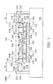
- FIG. 2 is a cross-sectional view of a semiconductor package assembly 500a.
- the semiconductor package assembly 500a includes a wire-bond ball-grid-array (BGA) semiconductor package 550a and a thermoelectric device chip 504 integrated within in accordance with some embodiments of the disclosure.
- the semiconductor package assembly 500a comprises a base 250, the wire-bond BGA semiconductor package 550a and a shielding case 232.
- the power system and the battery shown in FIG. 1 are not repeated for brevity.
- the base 250 for example a printed circuit board (PCB), may be formed of polypropylene (PP). It should also be noted that the base 250 can be a single layer or a multilayer structure.
- a plurality of conductive traces (not shown) and pads (not shown) is disposed on a device-attach surface 252 of the base 250.
- the conductive traces may comprise signal trace segments or ground trace segments, which are used for the input/output (I/O) connections of the BGA semiconductor package 550a.
- the pads are disposed on the device-attach surface 252, connecting to different terminals of the conductive traces. The pads are used for the wire-bond BGA semiconductor package 550a and the power system 600 as shown in FIG. 1 mounted directly thereon.
- the wire-bond BGA semiconductor package 550a is mounted on the device-attach surface 252 of the base 250 by a bonding process.
- the wire-bond BGA semiconductor package 550a is a package of large power consumption.
- the wire-bond BGA semiconductor package 550a may comprise a system-on-chip (SOC) package, a modem package, a radio-frequency (RF) module package including a power amplifier or a power management integrated circuit package.
- the SOC package may comprise a logic package.
- the wire-bond BGA semiconductor package 550a comprises a substrate 200, semiconductor dies 502a and 502b and a thermoelectric device chip 504a.
- the substrate 200 has a device-attach surface 201 and a bump-attach surface 203 opposite to the device-attach surface.
- the substrate 200 may comprise circuits 222, 224, 226, 228 and pads 202, 204, 206, 208, 222, 224, 226 and 228.
- the pads 202, 204, 206 and 208 are respectively disposed on the top of circuitries 222, 224, 226 and 228 close to the device-attach surface 201.
- the pads 222, 224, 226 and 228 are respectively disposed on the bottom of the circuitries 222, 224, 226 and 228 close to the bump-attach surface 203.
- the circuitries 222, 224, 226 and 228 of the wire-bond BGA semiconductor package 550a are interconnected with the circuitry of the base 200 via a plurality of conductive structures 240 disposed on the bump-attach surface 203 of the substrate 200. Also, the conductive structures 240 are in contact with the base 250.
- the conductive structures 240 may comprise a conductive bump structure such as a copper bump or a solder bump structure, a conductive pillar structure, a conductive wire structure, or a conductive paste structure.
- the semiconductor die 502a and 502b there are two semiconductor dies 502a and 502b attached to the substrate 200.
- the semiconductor die 502a is disposed on the device-attach surface 201 through an adhesion 501.
- the semiconductor die 502b is disposed on the semiconductor die 502a through an adhesion 503.
- the number of semiconductor dies is not limited to the disclosed embodiment.
- the semiconductor dies 502a and 502b may comprise a central processing unit (CPU), a graphics processing unit (GPU), a modem package, a power amplifier or a power management integrated circuit (PMIC) or any combination thereof.
- the semiconductor dies 502a and 502b are coupled to the pads 226 and 224 of the substrate 200 through bonding wires 508 and 506, respectively.
- thermoelectric device chip 504a is disposed over the semiconductor dies 502a and 502b, but separated from the semiconductor dies 502a and 502b through the molding compound 522. That is to say, the substrate 200 and the thermoelectric device chip 504a are disposed on opposite sides of the semiconductor dies 502a and 502b.
- the molding compound 522 covers the substrate 200 and surrounds the semiconductor dies 502a and 502b and thermoelectric device chip 504a, leaving a top surface 512 of the thermoelectric device chip 504a, a sidewall 230 and the bump-attach surface 203 of the substrate 200 exposed.
- the thermoelectric device chip 504a is arranged in a way that the top surface 512 is exposed to air, and the bottom surface 510 covered by the molding compound 522 is close to the semiconductor die 502b.
- the thermoelectric device chip 504a is configured to detect a heat energy (H T shown in FIG. 1 ) generated from the semiconductor dies 502a and 502b during operation.
- the heat energy results in a significant temperature difference between the top surface 512 and the bottom surface 510 of the thermoelectric device chip 504a. More specifically, the temperature of the bottom surface 510 is higher than that of the top surface 512 during operation of the semiconductor dies 502a and 502b.
- the thermoelectric device chip 504a can convert the detected temperature difference into an voltage difference between the top surface 512 and the bottom surface 510 of the thermoelectric device chip 504a.
- the thermoelectric device chip 504a comprises pads 514 and 516 coupled to the pads 222 and 228 of the substrate 200 by through mold vias (TMVs) 518 and 520 formed through the molding compound 522, respectively.
- the pads 514 and 516 are used to transmit an output current (I 2 shown in FIG. 1 ) translated from the voltage difference to the power system 600 as shown in FIG.
- thermoelectric device chip 504a senses the heat energy and converts into the current, the heat energy generated from the semiconductor dies 502a and 502b mainly dissipates through a path comprising the pads 204 and 206, the circuits 224 and 226 and the corresponding conductive structures 240.
- the shielding case 232 is disposed on the base 250.
- the shielding case 232 surrounds the wire-bond BGA semiconductor package 550a.
- the shielding case 232 has an opening 233 on the wire-bond BGA semiconductor package 550a, leaving the thermoelectric device chip 504a exposed by of the shielding case 232.
- An inner sidewall 234 of the shielding case 232 is spaced apart from a sidewall 524 of the wire-bond BGA semiconductor package 550a by a distance D.
- a space 238 surrounded by a sidewall 524 of the molding compound, the sidewall 230 of the substrate 200, the shielding case 232 and the base 250 is filled with air for the heat isolation function.
- the shielding case 232 may be formed by metal materials.
- an insulation film 236 may be conformably disposed on the inner sidewall 234 of the shielding case 232 for the improvement of the heat isolation function.
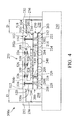
- FIG. 3 is a cross-sectional view of a semiconductor package assembly 500b including a flip-chip ball-grid-array (BGA) semiconductor package 550b and a thermoelectric device chip 504b integrated within in accordance with some embodiments of the disclosure. Elements of the embodiments hereinafter that are the same or similar as those previously described with reference to FIGS. 1 and 2 , are not repeated for brevity.
- the differences between the semiconductor package assembly 500a and semiconductor package assembly 500b comprise the flip-chip BGA semiconductor package 550b is fabricated using the flip-chip technology. Accordingly, a semiconductor die 502c of the flip-chip BGA semiconductor package 550b may be designed to be in contact with a thermoelectric device chip 504b packaged within.
- the flip-chip BGA semiconductor package 550b is a package of large power consumption with a function similar to the wire-bond BGA semiconductor package 550a.
- the flip-chip BGA semiconductor package 550b comprises at least one semiconductor die 502c turned upside down and mounted on the substrate 200 using the flip-chip technology. More specifically, the semiconductor die 502c has a top surface 507 and a bottom surface 505. The top surface 507 of the semiconductor die 502c is coupled to the pad 226 of the substrate 200 using solder balls 530 disposed thereon. The bottom surface 505 of the semiconductor die 502c is coupled to the thermoelectric device chip 504b using pads 528 disposed on. In this embodiment, the pads 528 of the semiconductor die 502c is in contact with corresponding pads 526 of the thermoelectric device chip 504b.
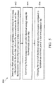
- FIG. 4 is a cross-sectional view of a semiconductor package assembly including a flip-chip ball-grid-array (BGA) semiconductor package 550c and a thermoelectric device chip 504c integrated within in accordance with some embodiments of the disclosure. Elements of the embodiments hereinafter that are the same or similar as those previously described with reference to FIGS. 1-3 , are not repeated for brevity.
- the semiconductor package assembly 500c and semiconductor package assembly 500b is that the semiconductor package assembly 500c comprises a semiconductor die 502c of the flip-chip BGA semiconductor package 550c may be designed to be separated from a thermoelectric device chip 504b packaged within.
- the flip-chip BGA semiconductor package 550c is a package of large power consumption with a function similar to the flip-chip BGA semiconductor package 550b.
- the semiconductor die 502c of the flip-chip BGA semiconductor package 550c has a top surface 507 and a bottom surface 505.
- the top surface 507 of the semiconductor die 502c is coupled to the pad 226 of the substrate 200 using solder balls 530 disposed thereon.
- the bottom surface 505 of the semiconductor die 502c is coupled to the thermoelectric device chip 504b using pads 528 disposed on.
- the pads 528 of the semiconductor die 502c is separated from corresponding pads 526 of the thermoelectric device chip 504c by conductive bumps 530.
- the pads 528 of the semiconductor die 502c and the pads 526 of the thermoelectric device chip 504c are in contact with the corresponding conductive bumps 530.
- FIG. 5 is a flow chart showing a method 800 for converting a thermal energy into an electrical energy in a portable electronic system as shown in FIG. 1 .
- the thermoelectric device chip 504 is used to detect a heat energy H T generated by operating a semiconductor die 502.
- the semiconductor die 502 and the thermoelectric device chip 504 are packaged within a semiconductor package, for example, the wire-bond BGA semiconductor package 550a and the flip-chip BGA semiconductor packages 550b-550c as shown in FIGS. 2-4 .
- FIGS. 1 the thermoelectric device chip 504 is used to detect a heat energy H T generated by operating a semiconductor die 502.
- the semiconductor die 502 and the thermoelectric device chip 504 are packaged within a semiconductor package, for example, the wire-bond BGA semiconductor package 550a and the flip-chip BGA semiconductor packages 550b-550c as shown in FIGS. 2-4 .
- each of the thermoelectric device chips 504a-504c has the bottom surface 510 close to the semiconductor die 502b-502c and the top surface 512 opposite to the bottom surface 510.
- Each of the thermoelectric device chips 504a-504c is arranged in such a way that the top surface 512 is exposed to air, and the bottom surface 510 is covered by the molding compound 522.
- the temperature of the bottom surface 510 is higher than that of the top surface 512 while operating the semiconductor dies 500a-500c (step 802).
- step 804 the heat energy H T is converted into a recycled electrical energy using the thermoelectric device chip 504 and then output as the current I 2 as shown in FIG. 1 .
- step 806 the recycled electrical energy (as the current I 2 ) is charged to a power system 600 as shown in FIG. 1 .
- the power system 600 is configured to distribute an electrical power to the semiconductor die 500 as shown in FIG. 1 .
- the step 806 further includes transmitting the recycled electrical energy to a charger of the power system 600 as shown in FIG. 1 , so that the charger stored the recycled electrical energy as a stored recycled electrical energy.
- the step 806 further includes translating the stored recycled electrical energy into the current I 2 to charge the battery 700 after transmitting the recycled electrical energy to a charger of the power system 600 as shown in FIG. 1 .
- Embodiments provide a portable electronic system with the thermal recycling function.
- the portable electronic system includes a thermal energy recycling semiconductor package having at least one semiconductor die with large power consumption and a thermoelectric device chip disposed close thereto.
- the portable electronic system allows the heat energy generated from the semiconductor die of the thermal energy recycling semiconductor package to be converted into a recycled electrical energy to be stored in the power system and charge the battery. Accordingly, the heat energy generated from the semiconductor die can be recycled to an electrical energy to provide to the portable electronic system.
Abstract
Description
- The present invention relates to a semiconductor package assembly, and in particular to a portable electronic system with a thermal recycling function.
- Portable devices have been developed to satisfy the requirements of low power consumption, high density, and high power efficiency. However, the heat dissipation problem limits the development of portable devices. For example, long-term-evolution (LTE) chips and other mobile chips require more power for high bandwidth transmission. The higher power consumption produces a higher rising temperature of the chips. The rising temperature of the chips results in heat dissipation problems, a reduced lifetime, and the slower transmission speeds.
- Thus, a novel semiconductor package assembly is desirable.
- An exemplary embodiment of a portable electronic system includes a semiconductor package. The semiconductor package includes a substrate. A semiconductor die is coupled to the substrate. A thermoelectric device chip is disposed close to the semiconductor die, coupled to the substrate. The thermoelectric device chip is configured to detect a heat energy generated from the semiconductor die and to convert the heat energy into a recycled electrical energy. A power system is coupled to the semiconductor package, configured to store the recycled electrical energy.
- Another exemplary embodiment of a semiconductor package assembly includes a base. A substrate is mounted on the base. A semiconductor die is coupled to the substrate. A thermoelectric device chip laminates on the semiconductor die. The thermoelectric device chip is configured to detect a heat energy generated from the semiconductor die and to convert the heat energy into a recycled electrical energy. A shielding case is disposed on the base. The shielding case surrounds the semiconductor package without covering a top surface of the thermoelectric device chip. A power system is mounted on the base and coupled to the thermoelectric device chip, configured to store the recycled electrical energy.
- An exemplary embodiment of a method for converting a thermal energy into an electrical energy in a portable electronic system includes detecting a heat energy generated by operating a semiconductor die using a thermoelectric device chip. The semiconductor die and the thermoelectric device chip are packaged within a semiconductor package. The heat energy is converted into a recycled electrical energy using the thermoelectric device chip. The recycled electrical energy is charged to a power system configured to distribute an electrical power to the semiconductor die.
- A detailed description is given in the following embodiments with reference to the accompanying drawings.
- The present invention can be more fully understood by reading the subsequent detailed description and examples with references made to the accompanying drawings, wherein:
-
FIG. 1 is a functional diagram of a portable electronic system showing the electrical energy transmission in accordance with some embodiments of the disclosure. -
FIG. 2 is a cross-sectional view of a semiconductor package assembly including a wire bond ball-grid-array (BGA) semiconductor package and a thermoelectric device chip integrated within in accordance with some embodiments of the disclosure. -
FIG. 3 is a cross-sectional view of a semiconductor package assembly including a flip-chip ball-grid-array (BGA) semiconductor package and a thermoelectric device chip integrated within in accordance with some embodiments of the disclosure. -
FIG. 4 is a cross-sectional view of a semiconductor package assembly including a flip-chip ball-grid-array (BGA) semiconductor package and a thermoelectric device chip integrated within in accordance with some embodiments of the disclosure. -
FIG. 5 is a flow chart showing a method for converting a thermal energy into an electrical energy in a portable electronic system as shown inFIG. 1 . - The following description is of the best-contemplated mode of carrying out the invention. This description is made for the purpose of illustrating the general principles of the invention and should not be taken in a limiting sense. The scope of the invention is determined by reference to the appended claims.
- The present invention will be described with respect to particular embodiments and with reference to certain drawings, but the invention is not limited thereto and is only limited by the claims. The drawings described are only schematic and are non-limiting. In the drawings, the size of some of the elements may be exaggerated for illustrative purposes and not drawn to scale. The dimensions and the relative dimensions do not correspond to actual dimensions in the practice of the invention.
-
FIG. 1 is a functional diagram of a portable electronic system showing the electrical and thermal energies transmission in accordance with some embodiments of the disclosure. As shown inFIG. 1 , the portable electronic system comprises asemiconductor package assembly 500, apower system 600 and abattery 700. In some embodiments, thesemiconductor package assembly 500 comprises asemiconductor die 502 and athermoelectric device chip 504 both packaged as a thermal energy recycling semiconductor package. Thepower system 600 is coupled to thesemiconductor package assembly 500 and thebattery 700. Thebattery 700 serves as a power source to output an electrical energy as a current I0 and supply to thepower system 600. Thepower system 600 is configured to distribute an electrical power as a current I1 from the current I0 to thesemiconductor package assembly 500 for the operation ofsemiconductor die 502. In some embodiments, the semiconductor die 502 generates a heat energy HT by the operation of the semiconductor die 502. Thethermoelectric device chip 504 is configured to detect the heat energy HT generated from thesemiconductor die 502 and to convert the heat energy HT into a recycled electrical energy and then output as a current I2 to thepower system 600. Thepower system 600 is also configured to store the recycled electrical energy as a stored recycled electrical energy and output as a current I3 to charge thebattery 700. Accordingly, the portable electronic system allows the heat energy generated from thesemiconductor die 502 of the thermal energy recycling semiconductor package to be converted into a recycled electrical energy to be stored in thepower system 600 and charge thebattery 700. -
FIG. 2 is a cross-sectional view of asemiconductor package assembly 500a. Thesemiconductor package assembly 500a includes a wire-bond ball-grid-array (BGA)semiconductor package 550a and athermoelectric device chip 504 integrated within in accordance with some embodiments of the disclosure. As shown inFIG. 2 , thesemiconductor package assembly 500a comprises abase 250, the wire-bondBGA semiconductor package 550a and ashielding case 232. To simplify the illustration, the power system and the battery shown inFIG. 1 are not repeated for brevity. - In some embodiments as shown in
FIG. 2 , thebase 250, for example a printed circuit board (PCB), may be formed of polypropylene (PP). It should also be noted that thebase 250 can be a single layer or a multilayer structure. A plurality of conductive traces (not shown) and pads (not shown) is disposed on a device-attach surface 252 of thebase 250. In one embodiment, the conductive traces may comprise signal trace segments or ground trace segments, which are used for the input/output (I/O) connections of theBGA semiconductor package 550a. Also, the pads are disposed on the device-attach surface 252, connecting to different terminals of the conductive traces. The pads are used for the wire-bondBGA semiconductor package 550a and thepower system 600 as shown inFIG. 1 mounted directly thereon. - As shown in
FIG. 2 , the wire-bondBGA semiconductor package 550a is mounted on the device-attach surface 252 of thebase 250 by a bonding process. In this embodiment, the wire-bondBGA semiconductor package 550a is a package of large power consumption. The wire-bondBGA semiconductor package 550a may comprise a system-on-chip (SOC) package, a modem package, a radio-frequency (RF) module package including a power amplifier or a power management integrated circuit package. For example, the SOC package may comprise a logic package. In some embodiments as shown inFIG. 2 , the wire-bondBGA semiconductor package 550a comprises a substrate 200, semiconductor dies 502a and 502b and athermoelectric device chip 504a. In some embodiments, the substrate 200 has a device-attachsurface 201 and a bump-attachsurface 203 opposite to the device-attach surface. The substrate 200 may comprisecircuits pads pads circuitries surface 201. Thepads circuitries surface 203. Thecircuitries BGA semiconductor package 550a are interconnected with the circuitry of the base 200 via a plurality ofconductive structures 240 disposed on the bump-attachsurface 203 of the substrate 200. Also, theconductive structures 240 are in contact with thebase 250. In one embodiment, theconductive structures 240 may comprise a conductive bump structure such as a copper bump or a solder bump structure, a conductive pillar structure, a conductive wire structure, or a conductive paste structure. - As shown in
FIG. 2 , there are two semiconductor dies 502a and 502b attached to the substrate 200. Thesemiconductor die 502a is disposed on the device-attachsurface 201 through anadhesion 501. Also, thesemiconductor die 502b is disposed on thesemiconductor die 502a through anadhesion 503. However, the number of semiconductor dies is not limited to the disclosed embodiment. In one embodiment, the semiconductor dies 502a and 502b may comprise a central processing unit (CPU), a graphics processing unit (GPU), a modem package, a power amplifier or a power management integrated circuit (PMIC) or any combination thereof. The semiconductor dies 502a and 502b are coupled to thepads bonding wires - As shown in
FIG. 2 , athermoelectric device chip 504a is disposed over the semiconductor dies 502a and 502b, but separated from the semiconductor dies 502a and 502b through themolding compound 522. That is to say, the substrate 200 and thethermoelectric device chip 504a are disposed on opposite sides of the semiconductor dies 502a and 502b. Themolding compound 522 covers the substrate 200 and surrounds the semiconductor dies 502a and 502b andthermoelectric device chip 504a, leaving atop surface 512 of thethermoelectric device chip 504a, asidewall 230 and the bump-attachsurface 203 of the substrate 200 exposed. Thethermoelectric device chip 504a is arranged in a way that thetop surface 512 is exposed to air, and the bottom surface 510 covered by themolding compound 522 is close to thesemiconductor die 502b. Thethermoelectric device chip 504a is configured to detect a heat energy (HT shown inFIG. 1 ) generated from the semiconductor dies 502a and 502b during operation. The heat energy results in a significant temperature difference between thetop surface 512 and the bottom surface 510 of thethermoelectric device chip 504a. More specifically, the temperature of the bottom surface 510 is higher than that of thetop surface 512 during operation of the semiconductor dies 502a and 502b. If the detected temperature difference is larger a specific value (for example, 50°C), thethermoelectric device chip 504a can convert the detected temperature difference into an voltage difference between thetop surface 512 and the bottom surface 510 of thethermoelectric device chip 504a. As shown inFIG. 2 , thethermoelectric device chip 504a comprisespads pads molding compound 522, respectively. Thepads FIG. 1 ) translated from the voltage difference to thepower system 600 as shown inFIG. 1 by theTMVs pads circuits conductive structures 240. Thepads circuits thermoelectric device chip 504a senses the heat energy and converts into the current, the heat energy generated from the semiconductor dies 502a and 502b mainly dissipates through a path comprising thepads circuits conductive structures 240. - As shown in
FIG. 2 , the shieldingcase 232 is disposed on thebase 250. The shieldingcase 232 surrounds the wire-bondBGA semiconductor package 550a. The shieldingcase 232 has anopening 233 on the wire-bondBGA semiconductor package 550a, leaving thethermoelectric device chip 504a exposed by of the shieldingcase 232. Aninner sidewall 234 of the shieldingcase 232 is spaced apart from a sidewall 524 of the wire-bondBGA semiconductor package 550a by a distanceD. A space 238 surrounded by a sidewall 524 of the molding compound, thesidewall 230 of the substrate 200, the shieldingcase 232 and thebase 250 is filled with air for the heat isolation function. In some embodiments, the shieldingcase 232 may be formed by metal materials. In some other embodiments, aninsulation film 236 may be conformably disposed on theinner sidewall 234 of the shieldingcase 232 for the improvement of the heat isolation function. -
FIG. 3 is a cross-sectional view of asemiconductor package assembly 500b including a flip-chip ball-grid-array (BGA)semiconductor package 550b and athermoelectric device chip 504b integrated within in accordance with some embodiments of the disclosure. Elements of the embodiments hereinafter that are the same or similar as those previously described with reference toFIGS. 1 and2 , are not repeated for brevity. The differences between thesemiconductor package assembly 500a andsemiconductor package assembly 500b comprise the flip-chipBGA semiconductor package 550b is fabricated using the flip-chip technology. Accordingly, asemiconductor die 502c of the flip-chipBGA semiconductor package 550b may be designed to be in contact with athermoelectric device chip 504b packaged within. - In this embodiment as shown in
FIG. 3 , the flip-chipBGA semiconductor package 550b is a package of large power consumption with a function similar to the wire-bondBGA semiconductor package 550a. The flip-chipBGA semiconductor package 550b comprises at least onesemiconductor die 502c turned upside down and mounted on the substrate 200 using the flip-chip technology. More specifically, thesemiconductor die 502c has atop surface 507 and abottom surface 505. Thetop surface 507 of thesemiconductor die 502c is coupled to thepad 226 of the substrate 200 usingsolder balls 530 disposed thereon. Thebottom surface 505 of thesemiconductor die 502c is coupled to thethermoelectric device chip 504b using pads 528 disposed on. In this embodiment, thepads 528 of thesemiconductor die 502c is in contact withcorresponding pads 526 of thethermoelectric device chip 504b. -
FIG. 4 is a cross-sectional view of a semiconductor package assembly including a flip-chip ball-grid-array (BGA)semiconductor package 550c and athermoelectric device chip 504c integrated within in accordance with some embodiments of the disclosure. Elements of the embodiments hereinafter that are the same or similar as those previously described with reference toFIGS. 1-3 , are not repeated for brevity. One of the differences between thesemiconductor package assembly 500c andsemiconductor package assembly 500b is that thesemiconductor package assembly 500c comprises asemiconductor die 502c of the flip-chipBGA semiconductor package 550c may be designed to be separated from athermoelectric device chip 504b packaged within. - In this embodiment as shown in
FIG. 4 , the flip-chipBGA semiconductor package 550c is a package of large power consumption with a function similar to the flip-chipBGA semiconductor package 550b. The semiconductor die 502c of the flip-chipBGA semiconductor package 550c has atop surface 507 and abottom surface 505. Thetop surface 507 of thesemiconductor die 502c is coupled to thepad 226 of the substrate 200 usingsolder balls 530 disposed thereon. Thebottom surface 505 of thesemiconductor die 502c is coupled to thethermoelectric device chip 504b using pads 528 disposed on. In this embodiment, thepads 528 of thesemiconductor die 502c is separated from correspondingpads 526 of thethermoelectric device chip 504c byconductive bumps 530. As shown inFIG. 4 , thepads 528 of thesemiconductor die 502c and thepads 526 of thethermoelectric device chip 504c are in contact with the correspondingconductive bumps 530. -
FIG. 5 is a flow chart showing amethod 800 for converting a thermal energy into an electrical energy in a portable electronic system as shown inFIG. 1 . Please refer toFIGS. 1 and5 , instep 802, thethermoelectric device chip 504 is used to detect a heat energy HT generated by operating asemiconductor die 502. It should be noted that the semiconductor die 502 and thethermoelectric device chip 504 are packaged within a semiconductor package, for example, the wire-bondBGA semiconductor package 550a and the flip-chip BGA semiconductor packages 550b-550c as shown inFIGS. 2-4 . Please refer toFIGS. 2-4 , each of thethermoelectric device chips 504a-504c has the bottom surface 510 close to the semiconductor die 502b-502c and thetop surface 512 opposite to the bottom surface 510. Each of thethermoelectric device chips 504a-504c is arranged in such a way that thetop surface 512 is exposed to air, and the bottom surface 510 is covered by themolding compound 522. The temperature of the bottom surface 510 is higher than that of thetop surface 512 while operating the semiconductor dies 500a-500c (step 802). - Next, in
step 804, the heat energy HT is converted into a recycled electrical energy using thethermoelectric device chip 504 and then output as the current I2 as shown inFIG. 1 . Next, instep 806, the recycled electrical energy (as the current I2) is charged to apower system 600 as shown inFIG. 1 . It should be noted that thepower system 600 is configured to distribute an electrical power to the semiconductor die 500 as shown inFIG. 1 . In some embodiments, thestep 806 further includes transmitting the recycled electrical energy to a charger of thepower system 600 as shown inFIG. 1 , so that the charger stored the recycled electrical energy as a stored recycled electrical energy. In some embodiments, thestep 806 further includes translating the stored recycled electrical energy into the current I2 to charge thebattery 700 after transmitting the recycled electrical energy to a charger of thepower system 600 as shown inFIG. 1 . - Embodiments provide a portable electronic system with the thermal recycling function. The portable electronic system includes a thermal energy recycling semiconductor package having at least one semiconductor die with large power consumption and a thermoelectric device chip disposed close thereto. The portable electronic system allows the heat energy generated from the semiconductor die of the thermal energy recycling semiconductor package to be converted into a recycled electrical energy to be stored in the power system and charge the battery. Accordingly, the heat energy generated from the semiconductor die can be recycled to an electrical energy to provide to the portable electronic system.
- While the invention has been described by way of example and in terms of the preferred embodiments, it is to be understood that the invention is not limited to the disclosed embodiments. On the contrary, it is intended to cover various modifications and similar arrangements (as would be apparent to those skilled in the art). Therefore, the scope of the appended claims should be accorded the broadest interpretation so as to encompass all such modifications and similar arrangements.
Claims (14)
Applications Claiming Priority (1)
| Application Number | Priority Date | Filing Date | Title |
|---|---|---|---|
| US14/717,159 US9837595B2 (en) | 2015-05-20 | 2015-05-20 | Semiconductor package assembly with thermal recycling function |
Publications (3)
| Publication Number | Publication Date |
|---|---|
| EP3096366A2 true EP3096366A2 (en) | 2016-11-23 |
| EP3096366A3 EP3096366A3 (en) | 2016-12-28 |
| EP3096366B1 EP3096366B1 (en) | 2019-05-01 |
Family
ID=53487256
Family Applications (1)
| Application Number | Title | Priority Date | Filing Date |
|---|---|---|---|
| EP15173493.6A Active EP3096366B1 (en) | 2015-05-20 | 2015-06-24 | Semiconductor package assembly with thermal recycling function |
Country Status (3)
| Country | Link |
|---|---|
| US (1) | US9837595B2 (en) |
| EP (1) | EP3096366B1 (en) |
| CN (1) | CN106169451B (en) |
Cited By (1)
| Publication number | Priority date | Publication date | Assignee | Title |
|---|---|---|---|---|
| EP3907757A1 (en) * | 2020-05-08 | 2021-11-10 | Samsung Electronics Co., Ltd. | Semiconductor package and electronic device including same |
Families Citing this family (9)
| Publication number | Priority date | Publication date | Assignee | Title |
|---|---|---|---|---|
| CN105340372A (en) * | 2013-07-30 | 2016-02-17 | 哈曼贝克自动系统股份有限公司 | Electronic module |
| US10665579B2 (en) * | 2016-02-16 | 2020-05-26 | Xilinx, Inc. | Chip package assembly with power management integrated circuit and integrated circuit die |
| US10600948B1 (en) * | 2016-11-28 | 2020-03-24 | Intel Corporation | Package with thermoelectric power feedback loop |
| US10504816B2 (en) | 2017-09-06 | 2019-12-10 | Google Llc | Thermoelectric cooler (TEC) for spot cooling of 2.5D/3D IC packages |
| US11784108B2 (en) | 2019-08-06 | 2023-10-10 | Intel Corporation | Thermal management in integrated circuit packages |
| US11830787B2 (en) | 2019-08-06 | 2023-11-28 | Intel Corporation | Thermal management in integrated circuit packages |
| US20210043543A1 (en) * | 2019-08-06 | 2021-02-11 | Intel Corporation | Thermal management in integrated circuit packages |
| KR20230025775A (en) | 2020-04-22 | 2023-02-23 | 유니버시티 오브 알칸소 테크놀러지 벤쳐스 | Devices for Harvesting Ambient Thermal and Vibrational Energy |
| CN112333978B (en) * | 2020-10-19 | 2023-06-06 | Oppo广东移动通信有限公司 | Heat dissipation assembly, electronic equipment and heat dissipation control method |
Family Cites Families (8)
| Publication number | Priority date | Publication date | Assignee | Title |
|---|---|---|---|---|
| JP3219055B2 (en) | 1998-06-26 | 2001-10-15 | 日本電気株式会社 | Electronic equipment |
| US20120038175A1 (en) * | 2009-04-15 | 2012-02-16 | Tang William S | Generating and using electricity derived from waste heat of an electrical appliance |
| CN101931347B (en) * | 2010-07-23 | 2014-07-30 | 惠州Tcl移动通信有限公司 | Method for raising energy consumption efficiency and mobile terminal thereof, and use of thermoelectric conversion module |
| JP5564455B2 (en) | 2011-03-17 | 2014-07-30 | 富士フイルム株式会社 | Thermoelectric generator and portable electronic device |
| US20140176041A1 (en) * | 2012-12-20 | 2014-06-26 | Nvidia Corporation | Semiconductor thermoelectric module charger for mobile computing device |
| US20140252531A1 (en) * | 2013-03-07 | 2014-09-11 | Qualcomm Incorporated | Systems and methods for harvesting dissipated heat from integrated circuits (ics) in electronic devices into electrical energy for providing power for the electronic devices |
| DE102013222163A1 (en) | 2013-10-31 | 2015-05-21 | Robert Bosch Gmbh | Electric circuit and method for producing an electrical circuit |
| US9491865B1 (en) * | 2015-04-24 | 2016-11-08 | Unimicron Technology Corp. | Circuit board and method for manufacturing the same |
-
2015
- 2015-05-20 US US14/717,159 patent/US9837595B2/en active Active
- 2015-06-24 EP EP15173493.6A patent/EP3096366B1/en active Active
-
2016
- 2016-05-19 CN CN201610332811.0A patent/CN106169451B/en active Active
Non-Patent Citations (1)
| Title |
|---|
| None |
Cited By (2)
| Publication number | Priority date | Publication date | Assignee | Title |
|---|---|---|---|---|
| EP3907757A1 (en) * | 2020-05-08 | 2021-11-10 | Samsung Electronics Co., Ltd. | Semiconductor package and electronic device including same |
| US11594262B2 (en) | 2020-05-08 | 2023-02-28 | Samsung Electronics Co., Ltd. | Semiconductor package and electronic device including same |
Also Published As
| Publication number | Publication date |
|---|---|
| US9837595B2 (en) | 2017-12-05 |
| CN106169451B (en) | 2019-01-22 |
| EP3096366B1 (en) | 2019-05-01 |
| US20160343929A1 (en) | 2016-11-24 |
| CN106169451A (en) | 2016-11-30 |
| EP3096366A3 (en) | 2016-12-28 |
Similar Documents
| Publication | Publication Date | Title |
|---|---|---|
| EP3096366B1 (en) | Semiconductor package assembly with thermal recycling function | |
| US10332830B2 (en) | Semiconductor package assembly | |
| TWI695478B (en) | Antenna module | |
| US9583430B2 (en) | Package-on-package device | |
| US9324696B2 (en) | Package-on-package devices, methods of fabricating the same, and semiconductor packages | |
| US10991638B2 (en) | Semiconductor package system | |
| US11075138B2 (en) | Semiconductor package system | |
| EP2996146A1 (en) | Semiconductor package assembly | |
| US20160005675A1 (en) | Double sided cooling chip package and method of manufacturing the same | |
| KR102186203B1 (en) | Package-on-package device including the same | |
| US20080093733A1 (en) | Chip package and manufacturing method thereof | |
| CN102859686B (en) | For width bus memory and serial storage being attached to the method for processor in wafer-level package area occupied | |
| KR20140130920A (en) | Package on package device and method of fabricating the device | |
| US10096534B2 (en) | Thermal performance of logic chip in a package-on-package structure | |
| CN103887258A (en) | Chip package using interposer substrate with through-silicon vias | |
| KR20120019091A (en) | Multi-chip package and method of manufacturing the same | |
| US20130329374A1 (en) | Pre-molded Cavity 3D Packaging Module with Layout | |
| KR20140111449A (en) | Semiconductor package and electronic system including the same | |
| US8288847B2 (en) | Dual die semiconductor package | |
| WO2013098929A1 (en) | Semiconductor chip and semiconductor module mounted with same | |
| US7592694B2 (en) | Chip package and method of manufacturing the same | |
| US9390992B2 (en) | Semiconductor packages including a metal layer between first and second semiconductor chips | |
| US11600607B2 (en) | Semiconductor module including multiple power management semiconductor packages | |
| US9601407B2 (en) | System-in-package module and method for forming the same | |
| CN112908945A (en) | Packaging assembly, electronic equipment and packaging method |
Legal Events
| Date | Code | Title | Description |
|---|---|---|---|
| PUAI | Public reference made under article 153(3) epc to a published international application that has entered the european phase |
Free format text: ORIGINAL CODE: 0009012 |
|
| AK | Designated contracting states |
Kind code of ref document: A2 Designated state(s): AL AT BE BG CH CY CZ DE DK EE ES FI FR GB GR HR HU IE IS IT LI LT LU LV MC MK MT NL NO PL PT RO RS SE SI SK SM TR |
|
| AX | Request for extension of the european patent |
Extension state: BA ME |
|
| PUAL | Search report despatched |
Free format text: ORIGINAL CODE: 0009013 |
|
| AK | Designated contracting states |
Kind code of ref document: A3 Designated state(s): AL AT BE BG CH CY CZ DE DK EE ES FI FR GB GR HR HU IE IS IT LI LT LU LV MC MK MT NL NO PL PT RO RS SE SI SK SM TR |
|
| AX | Request for extension of the european patent |
Extension state: BA ME |
|
| RIC1 | Information provided on ipc code assigned before grant |
Ipc: H01L 23/38 20060101ALI20161118BHEP Ipc: H01L 35/28 20060101AFI20161118BHEP |
|
| STAA | Information on the status of an ep patent application or granted ep patent |
Free format text: STATUS: REQUEST FOR EXAMINATION WAS MADE |
|
| 17P | Request for examination filed |
Effective date: 20170628 |
|
| RBV | Designated contracting states (corrected) |
Designated state(s): AL AT BE BG CH CY CZ DE DK EE ES FI FR GB GR HR HU IE IS IT LI LT LU LV MC MK MT NL NO PL PT RO RS SE SI SK SM TR |
|
| GRAP | Despatch of communication of intention to grant a patent |
Free format text: ORIGINAL CODE: EPIDOSNIGR1 |
|
| STAA | Information on the status of an ep patent application or granted ep patent |
Free format text: STATUS: GRANT OF PATENT IS INTENDED |
|
| INTG | Intention to grant announced |
Effective date: 20181212 |
|
| GRAS | Grant fee paid |
Free format text: ORIGINAL CODE: EPIDOSNIGR3 |
|
| GRAA | (expected) grant |
Free format text: ORIGINAL CODE: 0009210 |
|
| STAA | Information on the status of an ep patent application or granted ep patent |
Free format text: STATUS: THE PATENT HAS BEEN GRANTED |
|
| AK | Designated contracting states |
Kind code of ref document: B1 Designated state(s): AL AT BE BG CH CY CZ DE DK EE ES FI FR GB GR HR HU IE IS IT LI LT LU LV MC MK MT NL NO PL PT RO RS SE SI SK SM TR |
|
| REG | Reference to a national code |
Ref country code: GB Ref legal event code: FG4D |
|
| REG | Reference to a national code |
Ref country code: CH Ref legal event code: EP Ref country code: AT Ref legal event code: REF Ref document number: 1128103 Country of ref document: AT Kind code of ref document: T Effective date: 20190515 |
|
| REG | Reference to a national code |
Ref country code: DE Ref legal event code: R096 Ref document number: 602015029174 Country of ref document: DE |
|
| REG | Reference to a national code |
Ref country code: IE Ref legal event code: FG4D |
|
| REG | Reference to a national code |
Ref country code: NL Ref legal event code: MP Effective date: 20190501 |
|
| REG | Reference to a national code |
Ref country code: LT Ref legal event code: MG4D |
|
| PG25 | Lapsed in a contracting state [announced via postgrant information from national office to epo] |
Ref country code: FI Free format text: LAPSE BECAUSE OF FAILURE TO SUBMIT A TRANSLATION OF THE DESCRIPTION OR TO PAY THE FEE WITHIN THE PRESCRIBED TIME-LIMIT Effective date: 20190501 Ref country code: AL Free format text: LAPSE BECAUSE OF FAILURE TO SUBMIT A TRANSLATION OF THE DESCRIPTION OR TO PAY THE FEE WITHIN THE PRESCRIBED TIME-LIMIT Effective date: 20190501 Ref country code: NO Free format text: LAPSE BECAUSE OF FAILURE TO SUBMIT A TRANSLATION OF THE DESCRIPTION OR TO PAY THE FEE WITHIN THE PRESCRIBED TIME-LIMIT Effective date: 20190801 Ref country code: ES Free format text: LAPSE BECAUSE OF FAILURE TO SUBMIT A TRANSLATION OF THE DESCRIPTION OR TO PAY THE FEE WITHIN THE PRESCRIBED TIME-LIMIT Effective date: 20190501 Ref country code: HR Free format text: LAPSE BECAUSE OF FAILURE TO SUBMIT A TRANSLATION OF THE DESCRIPTION OR TO PAY THE FEE WITHIN THE PRESCRIBED TIME-LIMIT Effective date: 20190501 Ref country code: SE Free format text: LAPSE BECAUSE OF FAILURE TO SUBMIT A TRANSLATION OF THE DESCRIPTION OR TO PAY THE FEE WITHIN THE PRESCRIBED TIME-LIMIT Effective date: 20190501 Ref country code: LT Free format text: LAPSE BECAUSE OF FAILURE TO SUBMIT A TRANSLATION OF THE DESCRIPTION OR TO PAY THE FEE WITHIN THE PRESCRIBED TIME-LIMIT Effective date: 20190501 Ref country code: PT Free format text: LAPSE BECAUSE OF FAILURE TO SUBMIT A TRANSLATION OF THE DESCRIPTION OR TO PAY THE FEE WITHIN THE PRESCRIBED TIME-LIMIT Effective date: 20190901 Ref country code: NL Free format text: LAPSE BECAUSE OF FAILURE TO SUBMIT A TRANSLATION OF THE DESCRIPTION OR TO PAY THE FEE WITHIN THE PRESCRIBED TIME-LIMIT Effective date: 20190501 |
|
| PG25 | Lapsed in a contracting state [announced via postgrant information from national office to epo] |
Ref country code: RS Free format text: LAPSE BECAUSE OF FAILURE TO SUBMIT A TRANSLATION OF THE DESCRIPTION OR TO PAY THE FEE WITHIN THE PRESCRIBED TIME-LIMIT Effective date: 20190501 Ref country code: LV Free format text: LAPSE BECAUSE OF FAILURE TO SUBMIT A TRANSLATION OF THE DESCRIPTION OR TO PAY THE FEE WITHIN THE PRESCRIBED TIME-LIMIT Effective date: 20190501 Ref country code: GR Free format text: LAPSE BECAUSE OF FAILURE TO SUBMIT A TRANSLATION OF THE DESCRIPTION OR TO PAY THE FEE WITHIN THE PRESCRIBED TIME-LIMIT Effective date: 20190802 Ref country code: BG Free format text: LAPSE BECAUSE OF FAILURE TO SUBMIT A TRANSLATION OF THE DESCRIPTION OR TO PAY THE FEE WITHIN THE PRESCRIBED TIME-LIMIT Effective date: 20190801 |
|
| REG | Reference to a national code |
Ref country code: AT Ref legal event code: MK05 Ref document number: 1128103 Country of ref document: AT Kind code of ref document: T Effective date: 20190501 |
|
| PG25 | Lapsed in a contracting state [announced via postgrant information from national office to epo] |
Ref country code: IS Free format text: LAPSE BECAUSE OF FAILURE TO SUBMIT A TRANSLATION OF THE DESCRIPTION OR TO PAY THE FEE WITHIN THE PRESCRIBED TIME-LIMIT Effective date: 20190901 |
|
| PG25 | Lapsed in a contracting state [announced via postgrant information from national office to epo] |
Ref country code: CZ Free format text: LAPSE BECAUSE OF FAILURE TO SUBMIT A TRANSLATION OF THE DESCRIPTION OR TO PAY THE FEE WITHIN THE PRESCRIBED TIME-LIMIT Effective date: 20190501 Ref country code: MC Free format text: LAPSE BECAUSE OF FAILURE TO SUBMIT A TRANSLATION OF THE DESCRIPTION OR TO PAY THE FEE WITHIN THE PRESCRIBED TIME-LIMIT Effective date: 20190501 Ref country code: SK Free format text: LAPSE BECAUSE OF FAILURE TO SUBMIT A TRANSLATION OF THE DESCRIPTION OR TO PAY THE FEE WITHIN THE PRESCRIBED TIME-LIMIT Effective date: 20190501 Ref country code: AT Free format text: LAPSE BECAUSE OF FAILURE TO SUBMIT A TRANSLATION OF THE DESCRIPTION OR TO PAY THE FEE WITHIN THE PRESCRIBED TIME-LIMIT Effective date: 20190501 Ref country code: EE Free format text: LAPSE BECAUSE OF FAILURE TO SUBMIT A TRANSLATION OF THE DESCRIPTION OR TO PAY THE FEE WITHIN THE PRESCRIBED TIME-LIMIT Effective date: 20190501 Ref country code: DK Free format text: LAPSE BECAUSE OF FAILURE TO SUBMIT A TRANSLATION OF THE DESCRIPTION OR TO PAY THE FEE WITHIN THE PRESCRIBED TIME-LIMIT Effective date: 20190501 Ref country code: RO Free format text: LAPSE BECAUSE OF FAILURE TO SUBMIT A TRANSLATION OF THE DESCRIPTION OR TO PAY THE FEE WITHIN THE PRESCRIBED TIME-LIMIT Effective date: 20190501 |
|
| REG | Reference to a national code |
Ref country code: CH Ref legal event code: PL |
|
| REG | Reference to a national code |
Ref country code: DE Ref legal event code: R097 Ref document number: 602015029174 Country of ref document: DE |
|
| PG25 | Lapsed in a contracting state [announced via postgrant information from national office to epo] |
Ref country code: SM Free format text: LAPSE BECAUSE OF FAILURE TO SUBMIT A TRANSLATION OF THE DESCRIPTION OR TO PAY THE FEE WITHIN THE PRESCRIBED TIME-LIMIT Effective date: 20190501 Ref country code: IT Free format text: LAPSE BECAUSE OF FAILURE TO SUBMIT A TRANSLATION OF THE DESCRIPTION OR TO PAY THE FEE WITHIN THE PRESCRIBED TIME-LIMIT Effective date: 20190501 |
|
| PLBE | No opposition filed within time limit |
Free format text: ORIGINAL CODE: 0009261 |
|
| STAA | Information on the status of an ep patent application or granted ep patent |
Free format text: STATUS: NO OPPOSITION FILED WITHIN TIME LIMIT |
|
| REG | Reference to a national code |
Ref country code: BE Ref legal event code: MM Effective date: 20190630 |
|
| PG25 | Lapsed in a contracting state [announced via postgrant information from national office to epo] |
Ref country code: TR Free format text: LAPSE BECAUSE OF FAILURE TO SUBMIT A TRANSLATION OF THE DESCRIPTION OR TO PAY THE FEE WITHIN THE PRESCRIBED TIME-LIMIT Effective date: 20190501 |
|
| 26N | No opposition filed |
Effective date: 20200204 |
|
| PG25 | Lapsed in a contracting state [announced via postgrant information from national office to epo] |
Ref country code: PL Free format text: LAPSE BECAUSE OF FAILURE TO SUBMIT A TRANSLATION OF THE DESCRIPTION OR TO PAY THE FEE WITHIN THE PRESCRIBED TIME-LIMIT Effective date: 20190501 Ref country code: IE Free format text: LAPSE BECAUSE OF NON-PAYMENT OF DUE FEES Effective date: 20190624 |
|
| PG25 | Lapsed in a contracting state [announced via postgrant information from national office to epo] |
Ref country code: SI Free format text: LAPSE BECAUSE OF FAILURE TO SUBMIT A TRANSLATION OF THE DESCRIPTION OR TO PAY THE FEE WITHIN THE PRESCRIBED TIME-LIMIT Effective date: 20190501 Ref country code: LI Free format text: LAPSE BECAUSE OF NON-PAYMENT OF DUE FEES Effective date: 20190630 Ref country code: CH Free format text: LAPSE BECAUSE OF NON-PAYMENT OF DUE FEES Effective date: 20190630 Ref country code: LU Free format text: LAPSE BECAUSE OF NON-PAYMENT OF DUE FEES Effective date: 20190624 Ref country code: BE Free format text: LAPSE BECAUSE OF NON-PAYMENT OF DUE FEES Effective date: 20190630 |
|
| PG25 | Lapsed in a contracting state [announced via postgrant information from national office to epo] |
Ref country code: CY Free format text: LAPSE BECAUSE OF FAILURE TO SUBMIT A TRANSLATION OF THE DESCRIPTION OR TO PAY THE FEE WITHIN THE PRESCRIBED TIME-LIMIT Effective date: 20190501 |
|
| PG25 | Lapsed in a contracting state [announced via postgrant information from national office to epo] |
Ref country code: MT Free format text: LAPSE BECAUSE OF FAILURE TO SUBMIT A TRANSLATION OF THE DESCRIPTION OR TO PAY THE FEE WITHIN THE PRESCRIBED TIME-LIMIT Effective date: 20190501 Ref country code: HU Free format text: LAPSE BECAUSE OF FAILURE TO SUBMIT A TRANSLATION OF THE DESCRIPTION OR TO PAY THE FEE WITHIN THE PRESCRIBED TIME-LIMIT; INVALID AB INITIO Effective date: 20150624 |
|
| PG25 | Lapsed in a contracting state [announced via postgrant information from national office to epo] |
Ref country code: MK Free format text: LAPSE BECAUSE OF FAILURE TO SUBMIT A TRANSLATION OF THE DESCRIPTION OR TO PAY THE FEE WITHIN THE PRESCRIBED TIME-LIMIT Effective date: 20190501 |
|
| REG | Reference to a national code |
Ref country code: DE Ref legal event code: R079 Ref document number: 602015029174 Country of ref document: DE Free format text: PREVIOUS MAIN CLASS: H01L0035280000 Ipc: H10N0010100000 |
|
| P01 | Opt-out of the competence of the unified patent court (upc) registered |
Effective date: 20230607 |
|
| PGFP | Annual fee paid to national office [announced via postgrant information from national office to epo] |
Ref country code: FR Payment date: 20230626 Year of fee payment: 9 Ref country code: DE Payment date: 20230626 Year of fee payment: 9 |
|
| PGFP | Annual fee paid to national office [announced via postgrant information from national office to epo] |
Ref country code: GB Payment date: 20230627 Year of fee payment: 9 |