EP3096350A1 - Semiconductor package assembly and method for forming the same - Google Patents
Semiconductor package assembly and method for forming the same Download PDFInfo
- Publication number
- EP3096350A1 EP3096350A1 EP16166762.1A EP16166762A EP3096350A1 EP 3096350 A1 EP3096350 A1 EP 3096350A1 EP 16166762 A EP16166762 A EP 16166762A EP 3096350 A1 EP3096350 A1 EP 3096350A1
- Authority
- EP
- European Patent Office
- Prior art keywords
- semiconductor package
- semiconductor
- semiconductor die
- molding compound
- die
- Prior art date
- Legal status (The legal status is an assumption and is not a legal conclusion. Google has not performed a legal analysis and makes no representation as to the accuracy of the status listed.)
- Granted
Links
Images






Classifications
-
- H—ELECTRICITY
- H10—SEMICONDUCTOR DEVICES; ELECTRIC SOLID-STATE DEVICES NOT OTHERWISE PROVIDED FOR
- H10P—GENERIC PROCESSES OR APPARATUS FOR THE MANUFACTURE OR TREATMENT OF DEVICES COVERED BY CLASS H10
- H10P54/00—Cutting or separating of wafers, substrates or parts of devices
-
- H—ELECTRICITY
- H10—SEMICONDUCTOR DEVICES; ELECTRIC SOLID-STATE DEVICES NOT OTHERWISE PROVIDED FOR
- H10P—GENERIC PROCESSES OR APPARATUS FOR THE MANUFACTURE OR TREATMENT OF DEVICES COVERED BY CLASS H10
- H10P72/00—Handling or holding of wafers, substrates or devices during manufacture or treatment thereof
- H10P72/70—Handling or holding of wafers, substrates or devices during manufacture or treatment thereof for supporting or gripping
- H10P72/74—Handling or holding of wafers, substrates or devices during manufacture or treatment thereof for supporting or gripping using temporarily an auxiliary support
-
- H—ELECTRICITY
- H10—SEMICONDUCTOR DEVICES; ELECTRIC SOLID-STATE DEVICES NOT OTHERWISE PROVIDED FOR
- H10W—GENERIC PACKAGES, INTERCONNECTIONS, CONNECTORS OR OTHER CONSTRUCTIONAL DETAILS OF DEVICES COVERED BY CLASS H10
- H10W20/00—Interconnections in chips, wafers or substrates
- H10W20/01—Manufacture or treatment
- H10W20/031—Manufacture or treatment of conductive parts of the interconnections
- H10W20/056—Manufacture or treatment of conductive parts of the interconnections by filling conductive material into holes, grooves or trenches
- H10W20/057—Manufacture or treatment of conductive parts of the interconnections by filling conductive material into holes, grooves or trenches by selectively depositing, e.g. by using selective CVD or plating
-
- H—ELECTRICITY
- H10—SEMICONDUCTOR DEVICES; ELECTRIC SOLID-STATE DEVICES NOT OTHERWISE PROVIDED FOR
- H10W—GENERIC PACKAGES, INTERCONNECTIONS, CONNECTORS OR OTHER CONSTRUCTIONAL DETAILS OF DEVICES COVERED BY CLASS H10
- H10W20/00—Interconnections in chips, wafers or substrates
- H10W20/01—Manufacture or treatment
- H10W20/071—Manufacture or treatment of dielectric parts thereof
- H10W20/081—Manufacture or treatment of dielectric parts thereof by forming openings in the dielectric parts
-
- H—ELECTRICITY
- H10—SEMICONDUCTOR DEVICES; ELECTRIC SOLID-STATE DEVICES NOT OTHERWISE PROVIDED FOR
- H10W—GENERIC PACKAGES, INTERCONNECTIONS, CONNECTORS OR OTHER CONSTRUCTIONAL DETAILS OF DEVICES COVERED BY CLASS H10
- H10W20/00—Interconnections in chips, wafers or substrates
- H10W20/40—Interconnections external to wafers or substrates, e.g. back-end-of-line [BEOL] metallisations or vias connecting to gate electrodes
- H10W20/41—Interconnections external to wafers or substrates, e.g. back-end-of-line [BEOL] metallisations or vias connecting to gate electrodes characterised by their conductive parts
- H10W20/42—Vias, e.g. via plugs
-
- H—ELECTRICITY
- H10—SEMICONDUCTOR DEVICES; ELECTRIC SOLID-STATE DEVICES NOT OTHERWISE PROVIDED FOR
- H10W—GENERIC PACKAGES, INTERCONNECTIONS, CONNECTORS OR OTHER CONSTRUCTIONAL DETAILS OF DEVICES COVERED BY CLASS H10
- H10W20/00—Interconnections in chips, wafers or substrates
- H10W20/40—Interconnections external to wafers or substrates, e.g. back-end-of-line [BEOL] metallisations or vias connecting to gate electrodes
- H10W20/41—Interconnections external to wafers or substrates, e.g. back-end-of-line [BEOL] metallisations or vias connecting to gate electrodes characterised by their conductive parts
- H10W20/43—Layouts of interconnections
-
- H—ELECTRICITY
- H10—SEMICONDUCTOR DEVICES; ELECTRIC SOLID-STATE DEVICES NOT OTHERWISE PROVIDED FOR
- H10W—GENERIC PACKAGES, INTERCONNECTIONS, CONNECTORS OR OTHER CONSTRUCTIONAL DETAILS OF DEVICES COVERED BY CLASS H10
- H10W20/00—Interconnections in chips, wafers or substrates
- H10W20/40—Interconnections external to wafers or substrates, e.g. back-end-of-line [BEOL] metallisations or vias connecting to gate electrodes
- H10W20/41—Interconnections external to wafers or substrates, e.g. back-end-of-line [BEOL] metallisations or vias connecting to gate electrodes characterised by their conductive parts
- H10W20/44—Conductive materials thereof
- H10W20/4403—Conductive materials thereof based on metals, e.g. alloys, metal silicides
- H10W20/4421—Conductive materials thereof based on metals, e.g. alloys, metal silicides the principal metal being copper
-
- H—ELECTRICITY
- H10—SEMICONDUCTOR DEVICES; ELECTRIC SOLID-STATE DEVICES NOT OTHERWISE PROVIDED FOR
- H10W—GENERIC PACKAGES, INTERCONNECTIONS, CONNECTORS OR OTHER CONSTRUCTIONAL DETAILS OF DEVICES COVERED BY CLASS H10
- H10W70/00—Package substrates; Interposers; Redistribution layers [RDL]
- H10W70/01—Manufacture or treatment
- H10W70/05—Manufacture or treatment of insulating or insulated package substrates, or of interposers, or of redistribution layers
- H10W70/08—Manufacture or treatment of insulating or insulated package substrates, or of interposers, or of redistribution layers by depositing layers on the chip or wafer, e.g. "chip-first" RDLs
- H10W70/09—Manufacture or treatment of insulating or insulated package substrates, or of interposers, or of redistribution layers by depositing layers on the chip or wafer, e.g. "chip-first" RDLs extending onto an encapsulation that laterally surrounds the chip or wafer, e.g. fan-out wafer level package [FOWLP] RDLs
-
- H—ELECTRICITY
- H10—SEMICONDUCTOR DEVICES; ELECTRIC SOLID-STATE DEVICES NOT OTHERWISE PROVIDED FOR
- H10W—GENERIC PACKAGES, INTERCONNECTIONS, CONNECTORS OR OTHER CONSTRUCTIONAL DETAILS OF DEVICES COVERED BY CLASS H10
- H10W70/00—Package substrates; Interposers; Redistribution layers [RDL]
- H10W70/60—Insulating or insulated package substrates; Interposers; Redistribution layers
-
- H—ELECTRICITY
- H10—SEMICONDUCTOR DEVICES; ELECTRIC SOLID-STATE DEVICES NOT OTHERWISE PROVIDED FOR
- H10W—GENERIC PACKAGES, INTERCONNECTIONS, CONNECTORS OR OTHER CONSTRUCTIONAL DETAILS OF DEVICES COVERED BY CLASS H10
- H10W70/00—Package substrates; Interposers; Redistribution layers [RDL]
- H10W70/60—Insulating or insulated package substrates; Interposers; Redistribution layers
- H10W70/611—Insulating or insulated package substrates; Interposers; Redistribution layers for connecting multiple chips together
-
- H—ELECTRICITY
- H10—SEMICONDUCTOR DEVICES; ELECTRIC SOLID-STATE DEVICES NOT OTHERWISE PROVIDED FOR
- H10W—GENERIC PACKAGES, INTERCONNECTIONS, CONNECTORS OR OTHER CONSTRUCTIONAL DETAILS OF DEVICES COVERED BY CLASS H10
- H10W70/00—Package substrates; Interposers; Redistribution layers [RDL]
- H10W70/60—Insulating or insulated package substrates; Interposers; Redistribution layers
- H10W70/611—Insulating or insulated package substrates; Interposers; Redistribution layers for connecting multiple chips together
- H10W70/614—Insulating or insulated package substrates; Interposers; Redistribution layers for connecting multiple chips together the multiple chips being integrally enclosed
-
- H—ELECTRICITY
- H10—SEMICONDUCTOR DEVICES; ELECTRIC SOLID-STATE DEVICES NOT OTHERWISE PROVIDED FOR
- H10W—GENERIC PACKAGES, INTERCONNECTIONS, CONNECTORS OR OTHER CONSTRUCTIONAL DETAILS OF DEVICES COVERED BY CLASS H10
- H10W72/00—Interconnections or connectors in packages
-
- H—ELECTRICITY
- H10—SEMICONDUCTOR DEVICES; ELECTRIC SOLID-STATE DEVICES NOT OTHERWISE PROVIDED FOR
- H10W—GENERIC PACKAGES, INTERCONNECTIONS, CONNECTORS OR OTHER CONSTRUCTIONAL DETAILS OF DEVICES COVERED BY CLASS H10
- H10W72/00—Interconnections or connectors in packages
- H10W72/01—Manufacture or treatment
- H10W72/012—Manufacture or treatment of bump connectors, dummy bumps or thermal bumps
-
- H—ELECTRICITY
- H10—SEMICONDUCTOR DEVICES; ELECTRIC SOLID-STATE DEVICES NOT OTHERWISE PROVIDED FOR
- H10W—GENERIC PACKAGES, INTERCONNECTIONS, CONNECTORS OR OTHER CONSTRUCTIONAL DETAILS OF DEVICES COVERED BY CLASS H10
- H10W72/00—Interconnections or connectors in packages
- H10W72/20—Bump connectors, e.g. solder bumps or copper pillars; Dummy bumps; Thermal bumps
-
- H—ELECTRICITY
- H10—SEMICONDUCTOR DEVICES; ELECTRIC SOLID-STATE DEVICES NOT OTHERWISE PROVIDED FOR
- H10W—GENERIC PACKAGES, INTERCONNECTIONS, CONNECTORS OR OTHER CONSTRUCTIONAL DETAILS OF DEVICES COVERED BY CLASS H10
- H10W72/00—Interconnections or connectors in packages
- H10W72/90—Bond pads, in general
-
- H—ELECTRICITY
- H10—SEMICONDUCTOR DEVICES; ELECTRIC SOLID-STATE DEVICES NOT OTHERWISE PROVIDED FOR
- H10W—GENERIC PACKAGES, INTERCONNECTIONS, CONNECTORS OR OTHER CONSTRUCTIONAL DETAILS OF DEVICES COVERED BY CLASS H10
- H10W74/00—Encapsulations, e.g. protective coatings
- H10W74/01—Manufacture or treatment
- H10W74/012—Manufacture or treatment of encapsulations on active surfaces of flip-chip devices, e.g. forming underfills
-
- H—ELECTRICITY
- H10—SEMICONDUCTOR DEVICES; ELECTRIC SOLID-STATE DEVICES NOT OTHERWISE PROVIDED FOR
- H10W—GENERIC PACKAGES, INTERCONNECTIONS, CONNECTORS OR OTHER CONSTRUCTIONAL DETAILS OF DEVICES COVERED BY CLASS H10
- H10W74/00—Encapsulations, e.g. protective coatings
- H10W74/01—Manufacture or treatment
- H10W74/016—Manufacture or treatment using moulds
-
- H—ELECTRICITY
- H10—SEMICONDUCTOR DEVICES; ELECTRIC SOLID-STATE DEVICES NOT OTHERWISE PROVIDED FOR
- H10W—GENERIC PACKAGES, INTERCONNECTIONS, CONNECTORS OR OTHER CONSTRUCTIONAL DETAILS OF DEVICES COVERED BY CLASS H10
- H10W74/00—Encapsulations, e.g. protective coatings
- H10W74/10—Encapsulations, e.g. protective coatings characterised by their shape or disposition
- H10W74/111—Encapsulations, e.g. protective coatings characterised by their shape or disposition the semiconductor body being completely enclosed
- H10W74/129—Encapsulations, e.g. protective coatings characterised by their shape or disposition the semiconductor body being completely enclosed forming a chip-scale package [CSP]
-
- H—ELECTRICITY
- H10—SEMICONDUCTOR DEVICES; ELECTRIC SOLID-STATE DEVICES NOT OTHERWISE PROVIDED FOR
- H10W—GENERIC PACKAGES, INTERCONNECTIONS, CONNECTORS OR OTHER CONSTRUCTIONAL DETAILS OF DEVICES COVERED BY CLASS H10
- H10W74/00—Encapsulations, e.g. protective coatings
- H10W74/10—Encapsulations, e.g. protective coatings characterised by their shape or disposition
- H10W74/15—Encapsulations, e.g. protective coatings characterised by their shape or disposition on active surfaces of flip-chip devices, e.g. underfills
-
- H—ELECTRICITY
- H10—SEMICONDUCTOR DEVICES; ELECTRIC SOLID-STATE DEVICES NOT OTHERWISE PROVIDED FOR
- H10W—GENERIC PACKAGES, INTERCONNECTIONS, CONNECTORS OR OTHER CONSTRUCTIONAL DETAILS OF DEVICES COVERED BY CLASS H10
- H10W90/00—Package configurations
-
- H—ELECTRICITY
- H10—SEMICONDUCTOR DEVICES; ELECTRIC SOLID-STATE DEVICES NOT OTHERWISE PROVIDED FOR
- H10W—GENERIC PACKAGES, INTERCONNECTIONS, CONNECTORS OR OTHER CONSTRUCTIONAL DETAILS OF DEVICES COVERED BY CLASS H10
- H10W90/00—Package configurations
- H10W90/401—Package configurations characterised by multiple insulating or insulated package substrates, interposers or RDLs
-
- H—ELECTRICITY
- H10—SEMICONDUCTOR DEVICES; ELECTRIC SOLID-STATE DEVICES NOT OTHERWISE PROVIDED FOR
- H10W—GENERIC PACKAGES, INTERCONNECTIONS, CONNECTORS OR OTHER CONSTRUCTIONAL DETAILS OF DEVICES COVERED BY CLASS H10
- H10W70/00—Package substrates; Interposers; Redistribution layers [RDL]
- H10W70/01—Manufacture or treatment
- H10W70/05—Manufacture or treatment of insulating or insulated package substrates, or of interposers, or of redistribution layers
-
- H—ELECTRICITY
- H10—SEMICONDUCTOR DEVICES; ELECTRIC SOLID-STATE DEVICES NOT OTHERWISE PROVIDED FOR
- H10W—GENERIC PACKAGES, INTERCONNECTIONS, CONNECTORS OR OTHER CONSTRUCTIONAL DETAILS OF DEVICES COVERED BY CLASS H10
- H10W70/00—Package substrates; Interposers; Redistribution layers [RDL]
- H10W70/60—Insulating or insulated package substrates; Interposers; Redistribution layers
- H10W70/62—Insulating or insulated package substrates; Interposers; Redistribution layers characterised by their interconnections
- H10W70/65—Shapes or dispositions of interconnections
-
- H—ELECTRICITY
- H10—SEMICONDUCTOR DEVICES; ELECTRIC SOLID-STATE DEVICES NOT OTHERWISE PROVIDED FOR
- H10W—GENERIC PACKAGES, INTERCONNECTIONS, CONNECTORS OR OTHER CONSTRUCTIONAL DETAILS OF DEVICES COVERED BY CLASS H10
- H10W70/00—Package substrates; Interposers; Redistribution layers [RDL]
- H10W70/60—Insulating or insulated package substrates; Interposers; Redistribution layers
- H10W70/62—Insulating or insulated package substrates; Interposers; Redistribution layers characterised by their interconnections
- H10W70/65—Shapes or dispositions of interconnections
- H10W70/654—Top-view layouts
- H10W70/655—Fan-out layouts
-
- H—ELECTRICITY
- H10—SEMICONDUCTOR DEVICES; ELECTRIC SOLID-STATE DEVICES NOT OTHERWISE PROVIDED FOR
- H10W—GENERIC PACKAGES, INTERCONNECTIONS, CONNECTORS OR OTHER CONSTRUCTIONAL DETAILS OF DEVICES COVERED BY CLASS H10
- H10W72/00—Interconnections or connectors in packages
- H10W72/01—Manufacture or treatment
- H10W72/019—Manufacture or treatment of bond pads
- H10W72/01904—Manufacture or treatment of bond pads using temporary auxiliary members, e.g. using sacrificial coatings or handle substrates
-
- H—ELECTRICITY
- H10—SEMICONDUCTOR DEVICES; ELECTRIC SOLID-STATE DEVICES NOT OTHERWISE PROVIDED FOR
- H10W—GENERIC PACKAGES, INTERCONNECTIONS, CONNECTORS OR OTHER CONSTRUCTIONAL DETAILS OF DEVICES COVERED BY CLASS H10
- H10W72/00—Interconnections or connectors in packages
- H10W72/01—Manufacture or treatment
- H10W72/0198—Manufacture or treatment batch processes
-
- H—ELECTRICITY
- H10—SEMICONDUCTOR DEVICES; ELECTRIC SOLID-STATE DEVICES NOT OTHERWISE PROVIDED FOR
- H10W—GENERIC PACKAGES, INTERCONNECTIONS, CONNECTORS OR OTHER CONSTRUCTIONAL DETAILS OF DEVICES COVERED BY CLASS H10
- H10W72/00—Interconnections or connectors in packages
- H10W72/071—Connecting or disconnecting
- H10W72/072—Connecting or disconnecting of bump connectors
- H10W72/07231—Techniques
- H10W72/07236—Soldering or alloying
-
- H—ELECTRICITY
- H10—SEMICONDUCTOR DEVICES; ELECTRIC SOLID-STATE DEVICES NOT OTHERWISE PROVIDED FOR
- H10W—GENERIC PACKAGES, INTERCONNECTIONS, CONNECTORS OR OTHER CONSTRUCTIONAL DETAILS OF DEVICES COVERED BY CLASS H10
- H10W72/00—Interconnections or connectors in packages
- H10W72/071—Connecting or disconnecting
- H10W72/073—Connecting or disconnecting of die-attach connectors
- H10W72/07331—Connecting techniques
-
- H—ELECTRICITY
- H10—SEMICONDUCTOR DEVICES; ELECTRIC SOLID-STATE DEVICES NOT OTHERWISE PROVIDED FOR
- H10W—GENERIC PACKAGES, INTERCONNECTIONS, CONNECTORS OR OTHER CONSTRUCTIONAL DETAILS OF DEVICES COVERED BY CLASS H10
- H10W72/00—Interconnections or connectors in packages
- H10W72/20—Bump connectors, e.g. solder bumps or copper pillars; Dummy bumps; Thermal bumps
- H10W72/241—Dispositions, e.g. layouts
-
- H—ELECTRICITY
- H10—SEMICONDUCTOR DEVICES; ELECTRIC SOLID-STATE DEVICES NOT OTHERWISE PROVIDED FOR
- H10W—GENERIC PACKAGES, INTERCONNECTIONS, CONNECTORS OR OTHER CONSTRUCTIONAL DETAILS OF DEVICES COVERED BY CLASS H10
- H10W72/00—Interconnections or connectors in packages
- H10W72/20—Bump connectors, e.g. solder bumps or copper pillars; Dummy bumps; Thermal bumps
- H10W72/241—Dispositions, e.g. layouts
- H10W72/242—Dispositions, e.g. layouts relative to the surface, e.g. recessed, protruding
-
- H—ELECTRICITY
- H10—SEMICONDUCTOR DEVICES; ELECTRIC SOLID-STATE DEVICES NOT OTHERWISE PROVIDED FOR
- H10W—GENERIC PACKAGES, INTERCONNECTIONS, CONNECTORS OR OTHER CONSTRUCTIONAL DETAILS OF DEVICES COVERED BY CLASS H10
- H10W72/00—Interconnections or connectors in packages
- H10W72/20—Bump connectors, e.g. solder bumps or copper pillars; Dummy bumps; Thermal bumps
- H10W72/241—Dispositions, e.g. layouts
- H10W72/244—Dispositions, e.g. layouts relative to underlying supporting features, e.g. bond pads, RDLs or vias
-
- H—ELECTRICITY
- H10—SEMICONDUCTOR DEVICES; ELECTRIC SOLID-STATE DEVICES NOT OTHERWISE PROVIDED FOR
- H10W—GENERIC PACKAGES, INTERCONNECTIONS, CONNECTORS OR OTHER CONSTRUCTIONAL DETAILS OF DEVICES COVERED BY CLASS H10
- H10W72/00—Interconnections or connectors in packages
- H10W72/20—Bump connectors, e.g. solder bumps or copper pillars; Dummy bumps; Thermal bumps
- H10W72/251—Materials
- H10W72/252—Materials comprising solid metals or solid metalloids, e.g. PbSn, Ag or Cu
-
- H—ELECTRICITY
- H10—SEMICONDUCTOR DEVICES; ELECTRIC SOLID-STATE DEVICES NOT OTHERWISE PROVIDED FOR
- H10W—GENERIC PACKAGES, INTERCONNECTIONS, CONNECTORS OR OTHER CONSTRUCTIONAL DETAILS OF DEVICES COVERED BY CLASS H10
- H10W72/00—Interconnections or connectors in packages
- H10W72/851—Dispositions of multiple connectors or interconnections
- H10W72/874—On different surfaces
-
- H—ELECTRICITY
- H10—SEMICONDUCTOR DEVICES; ELECTRIC SOLID-STATE DEVICES NOT OTHERWISE PROVIDED FOR
- H10W—GENERIC PACKAGES, INTERCONNECTIONS, CONNECTORS OR OTHER CONSTRUCTIONAL DETAILS OF DEVICES COVERED BY CLASS H10
- H10W72/00—Interconnections or connectors in packages
- H10W72/90—Bond pads, in general
- H10W72/921—Structures or relative sizes of bond pads
- H10W72/922—Bond pads being integral with underlying chip-level interconnections
-
- H—ELECTRICITY
- H10—SEMICONDUCTOR DEVICES; ELECTRIC SOLID-STATE DEVICES NOT OTHERWISE PROVIDED FOR
- H10W—GENERIC PACKAGES, INTERCONNECTIONS, CONNECTORS OR OTHER CONSTRUCTIONAL DETAILS OF DEVICES COVERED BY CLASS H10
- H10W72/00—Interconnections or connectors in packages
- H10W72/90—Bond pads, in general
- H10W72/941—Dispositions of bond pads
-
- H—ELECTRICITY
- H10—SEMICONDUCTOR DEVICES; ELECTRIC SOLID-STATE DEVICES NOT OTHERWISE PROVIDED FOR
- H10W—GENERIC PACKAGES, INTERCONNECTIONS, CONNECTORS OR OTHER CONSTRUCTIONAL DETAILS OF DEVICES COVERED BY CLASS H10
- H10W72/00—Interconnections or connectors in packages
- H10W72/90—Bond pads, in general
- H10W72/941—Dispositions of bond pads
- H10W72/9413—Dispositions of bond pads on encapsulations
-
- H—ELECTRICITY
- H10—SEMICONDUCTOR DEVICES; ELECTRIC SOLID-STATE DEVICES NOT OTHERWISE PROVIDED FOR
- H10W—GENERIC PACKAGES, INTERCONNECTIONS, CONNECTORS OR OTHER CONSTRUCTIONAL DETAILS OF DEVICES COVERED BY CLASS H10
- H10W72/00—Interconnections or connectors in packages
- H10W72/90—Bond pads, in general
- H10W72/941—Dispositions of bond pads
- H10W72/9415—Dispositions of bond pads relative to the surface, e.g. recessed, protruding
-
- H—ELECTRICITY
- H10—SEMICONDUCTOR DEVICES; ELECTRIC SOLID-STATE DEVICES NOT OTHERWISE PROVIDED FOR
- H10W—GENERIC PACKAGES, INTERCONNECTIONS, CONNECTORS OR OTHER CONSTRUCTIONAL DETAILS OF DEVICES COVERED BY CLASS H10
- H10W72/00—Interconnections or connectors in packages
- H10W72/90—Bond pads, in general
- H10W72/951—Materials of bond pads
- H10W72/952—Materials of bond pads comprising metals or metalloids, e.g. PbSn, Ag or Cu
-
- H—ELECTRICITY
- H10—SEMICONDUCTOR DEVICES; ELECTRIC SOLID-STATE DEVICES NOT OTHERWISE PROVIDED FOR
- H10W—GENERIC PACKAGES, INTERCONNECTIONS, CONNECTORS OR OTHER CONSTRUCTIONAL DETAILS OF DEVICES COVERED BY CLASS H10
- H10W74/00—Encapsulations, e.g. protective coatings
- H10W74/01—Manufacture or treatment
- H10W74/014—Manufacture or treatment using batch processing
-
- H—ELECTRICITY
- H10—SEMICONDUCTOR DEVICES; ELECTRIC SOLID-STATE DEVICES NOT OTHERWISE PROVIDED FOR
- H10W—GENERIC PACKAGES, INTERCONNECTIONS, CONNECTORS OR OTHER CONSTRUCTIONAL DETAILS OF DEVICES COVERED BY CLASS H10
- H10W74/00—Encapsulations, e.g. protective coatings
- H10W74/01—Manufacture or treatment
- H10W74/019—Manufacture or treatment using temporary auxiliary substrates
-
- H—ELECTRICITY
- H10—SEMICONDUCTOR DEVICES; ELECTRIC SOLID-STATE DEVICES NOT OTHERWISE PROVIDED FOR
- H10W—GENERIC PACKAGES, INTERCONNECTIONS, CONNECTORS OR OTHER CONSTRUCTIONAL DETAILS OF DEVICES COVERED BY CLASS H10
- H10W74/00—Encapsulations, e.g. protective coatings
- H10W74/10—Encapsulations, e.g. protective coatings characterised by their shape or disposition
- H10W74/131—Encapsulations, e.g. protective coatings characterised by their shape or disposition the semiconductor body being only partially enclosed
- H10W74/142—Encapsulations, e.g. protective coatings characterised by their shape or disposition the semiconductor body being only partially enclosed the encapsulations exposing the passive side of the semiconductor body
-
- H—ELECTRICITY
- H10—SEMICONDUCTOR DEVICES; ELECTRIC SOLID-STATE DEVICES NOT OTHERWISE PROVIDED FOR
- H10W—GENERIC PACKAGES, INTERCONNECTIONS, CONNECTORS OR OTHER CONSTRUCTIONAL DETAILS OF DEVICES COVERED BY CLASS H10
- H10W80/00—Direct bonding of chips, wafers or substrates
- H10W80/211—Direct bonding of chips, wafers or substrates using auxiliary members, e.g. aids for protecting the bonding area
-
- H—ELECTRICITY
- H10—SEMICONDUCTOR DEVICES; ELECTRIC SOLID-STATE DEVICES NOT OTHERWISE PROVIDED FOR
- H10W—GENERIC PACKAGES, INTERCONNECTIONS, CONNECTORS OR OTHER CONSTRUCTIONAL DETAILS OF DEVICES COVERED BY CLASS H10
- H10W80/00—Direct bonding of chips, wafers or substrates
- H10W80/301—Bonding techniques, e.g. hybrid bonding
- H10W80/312—Bonding techniques, e.g. hybrid bonding characterised by the direct bonding of electrically conductive pads
-
- H—ELECTRICITY
- H10—SEMICONDUCTOR DEVICES; ELECTRIC SOLID-STATE DEVICES NOT OTHERWISE PROVIDED FOR
- H10W—GENERIC PACKAGES, INTERCONNECTIONS, CONNECTORS OR OTHER CONSTRUCTIONAL DETAILS OF DEVICES COVERED BY CLASS H10
- H10W80/00—Direct bonding of chips, wafers or substrates
- H10W80/301—Bonding techniques, e.g. hybrid bonding
- H10W80/327—Bonding techniques, e.g. hybrid bonding characterised by the direct bonding of insulating parts, e.g. of silicon oxide layers
-
- H—ELECTRICITY
- H10—SEMICONDUCTOR DEVICES; ELECTRIC SOLID-STATE DEVICES NOT OTHERWISE PROVIDED FOR
- H10W—GENERIC PACKAGES, INTERCONNECTIONS, CONNECTORS OR OTHER CONSTRUCTIONAL DETAILS OF DEVICES COVERED BY CLASS H10
- H10W80/00—Direct bonding of chips, wafers or substrates
- H10W80/301—Bonding techniques, e.g. hybrid bonding
- H10W80/331—Bonding techniques, e.g. hybrid bonding characterised by the application of energy for connecting
-
- H—ELECTRICITY
- H10—SEMICONDUCTOR DEVICES; ELECTRIC SOLID-STATE DEVICES NOT OTHERWISE PROVIDED FOR
- H10W—GENERIC PACKAGES, INTERCONNECTIONS, CONNECTORS OR OTHER CONSTRUCTIONAL DETAILS OF DEVICES COVERED BY CLASS H10
- H10W90/00—Package configurations
- H10W90/701—Package configurations characterised by the relative positions of pads or connectors relative to package parts
-
- H—ELECTRICITY
- H10—SEMICONDUCTOR DEVICES; ELECTRIC SOLID-STATE DEVICES NOT OTHERWISE PROVIDED FOR
- H10W—GENERIC PACKAGES, INTERCONNECTIONS, CONNECTORS OR OTHER CONSTRUCTIONAL DETAILS OF DEVICES COVERED BY CLASS H10
- H10W90/00—Package configurations
- H10W90/701—Package configurations characterised by the relative positions of pads or connectors relative to package parts
- H10W90/791—Package configurations characterised by the relative positions of pads or connectors relative to package parts of direct-bonded pads
- H10W90/792—Package configurations characterised by the relative positions of pads or connectors relative to package parts of direct-bonded pads between multiple chips
-
- H—ELECTRICITY
- H10—SEMICONDUCTOR DEVICES; ELECTRIC SOLID-STATE DEVICES NOT OTHERWISE PROVIDED FOR
- H10W—GENERIC PACKAGES, INTERCONNECTIONS, CONNECTORS OR OTHER CONSTRUCTIONAL DETAILS OF DEVICES COVERED BY CLASS H10
- H10W99/00—Subject matter not provided for in other groups of this subclass
Definitions
- the present invention relates to a semiconductor package assembly, and in particular to a three-dimensional (3D) semiconductor package assembly and methods for forming the same.
- 3D integrated circuits and stacked dies have been developed and are commonly used, the dies integrated into a conventional 3D semiconductor package are limited to be the same size. Furthermore, 3D semiconductor packaging technology suffers from various problems that may cause a reduction of the manufacturing yield.
- a semiconductor package assembly and a method for forming a semiconductor package assembly are provided.
- An exemplary embodiment of a semiconductor package assembly includes a first semiconductor package.
- the first semiconductor package includes a first semiconductor die.
- a first redistribution layer (RDL) structure is coupled to the first semiconductor die and includes a first conductive trace.
- the semiconductor package assembly also includes a second semiconductor package bonded to the first semiconductor package.
- the second semiconductor package includes a second semiconductor die.
- An active surface of the second semiconductor die faces an active surface of the first semiconductor die.
- a second RDL structure is coupled to the second semiconductor die and includes a second conductive trace. The first conductive trace is in direct contact with the second conductive trace.
- a semiconductor package assembly includes a first package.
- the first package includes a first component.
- a first RDL structure is coupled to the first component and includes a first conductive trace.
- the semiconductor package assembly also includes a second package bonded to the first package.
- the second package includes a second component.
- a second RDL structure is coupled to the second component and includes a second conductive trace. The first conductive trace is in direct contact with the second conductive trace.
- An exemplary embodiment of a method for forming a semiconductor package assembly includes forming a first semiconductor package.
- the first semiconductor package includes a first semiconductor die.
- a first RDL structure is coupled to the first semiconductor die and includes a first conductive trace.
- the method also includes forming a second semiconductor package.
- the second semiconductor package includes a second semiconductor die.
- An active surface of the second semiconductor die faces an active surface of the first semiconductor die.
- a second RDL structure is coupled to the second semiconductor die and includes a second conductive trace.
- the method further includes bonding the second semiconductor package to the first semiconductor package.
- the first conductive trace is in direct contact with the second conductive trace.
- Embodiments of the disclosure provide a 3D system-in-package (SIP) semiconductor package assembly.
- the semiconductor package assembly is integrated with more than two components or dies so that the size of electronic products made using the semiconductor package assembly can be reduced.
- These components or dies are separately fabricated and are subsequently integrated into the semiconductor package assembly. As a result, their sizes and/or functions are not limited to be the same.
- the design flexibility of the semiconductor package assembly is greatly improved.
- these components or dies are tested in advance to make sure that the semiconductor package assembly only includes good components or dies. As a result, the yield loss resulted from multiple defective components or dies is significantly mitigated or eliminated. Therefore, the manufacturing cost of the semiconductor package assembly is reduced.
- FIGS. 1A-1C are cross-sectional views of various stages of a method for forming a semiconductor package, in accordance with some embodiments of the disclosure. Additional operations can be provided before, during, and/or after the stages described in FIGS. 1A-1C . Some of the stages that are described can be replaced or eliminated for different embodiments. Additional features can be added to the semiconductor package. Some of the features described below can be replaced or eliminated for different embodiments.
- a first carrier substrate 100A is provided.
- the first carrier substrate 100A is a wafer or a panel.
- the first carrier substrate 100A may include glass or another suitable supporting material.
- first components 110A are bonded onto the first carrier substrate 100A.
- the first components 110A are known-good components. In other words, no defective components are bonded onto the first carrier substrate 100A.
- the first components 110A and the first carrier substrate 100A are attached together through an adhesive layer such as glue or another suitable adhesive material.
- the first components 110A are active devices and can be referred to as first semiconductor dies (or chips) 110A.
- the first semiconductor dies 110A may include transistors or another suitable active element.
- the first semiconductor dies 110A may be a logic die including a central processing unit (CPU), a graphics processing unit (GPU), a dynamic random access memory (DRAM) controller or any combination thereof.
- the first components 110A are passive devices such as integrated passive devices (IPDs).
- the first components 110A may include capacitors, resistors, inductors, varactor diodes or another suitable passive element.
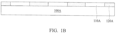
- a first molding compound 120A is formed on the first carrier substrate 100A.
- the first molding compound 120A surrounds the sidewalls of the first components 110A without covering the top and bottom surfaces of the first components 110A.
- the first molding compound 120A is formed of a nonconductive material such as an epoxy, a resin, a moldable polymer, or another suitable molding material.
- the first molding compound 120A is applied as a substantial liquid, and then is cured through a chemical reaction.
- the first molding compound 120A is an ultraviolet (UV) or thermally cured polymer applied as a gel or malleable solid, and then is cured through a UV or thermal curing process. The first molding compound 120A may be cured with a mold.
- the deposited first molding compound 120A covers the top surfaces of the first components 110A, and then a grinding process is performed to thin the deposited first molding compound 120A. As a result, the thinned first molding compound 120A exposes the top surfaces of the first components 110A. In some embodiments, the top and bottom surfaces of the first molding compound 120A are coplanar with the top and bottom surfaces of the first components 110A, respectively.
- a first redistribution layer (RDL) structure 130A which is also referred to as a fan-out structure, is formed on the first molding compound 120A and is coupled to the first components 110A.
- RDL redistribution layer
- a first (semiconductor) package A is formed.
- the first (semiconductor) package A is a wafer-level fan-out package.
- the first RDL structure 130A covers the first molding compound 120A and may be in direct contact with the first molding compound 120A.
- the first RDL structure 130A includes one or more conductive traces 140A disposed in and surrounded by an inter-metal dielectric (IMD) layer 150A.
- the first components 110A are electrically connected to the conductive traces 140A of the first RDL structure 130A.
- the IMD layer 150A may include multiple sub-dielectric layers successively stacked on the first molding compound 120A and the first components 110A. For example, a first layer-level of the conductive traces 140A is positioned on a first layer-level of the sub-dielectric layers and covered by a second layer-level of the sub-dielectric layers. A second layer-level of the conductive traces 140A is positioned on the second layer-level of the sub-dielectric layers and covered by a third layer-level of the sub-dielectric layers.
- the IMD layer 150A may be formed of organic materials, which include a polymer base material, non-organic materials, which include silicon nitride (SiN X ), silicon oxide (SiO X ), graphene, or the like.
- the IMD layer 150A is a high-k dielectric layer (k is the dielectric constant of the dielectric layer).
- the IMD layer 150A may be formed of a photosensitive material, which includes a dry film photoresist, or a taping film.
- Pad portions of the conductive traces 140A are exposed from the top surface of the first RDL structure 130A.
- the pad portions of the conductive traces 140A are exposed from openings of the IMD layer 150A and connected to subsequently formed conductive components.
- the number and configuration of the conductive trace 140A and the IMD layer 150A shown in figures are only examples and are not limitations to the present invention.
- the conductive traces 140A include copper, or another suitable conductive material with good diffusibility.
- FIGS. 2A-2C are cross-sectional views of various stages of a method for forming a semiconductor package, in accordance with some embodiments of the disclosure. Additional operations can be provided before, during, and/or after the stages described in FIGS. 2A-2C . Some of the stages that are described can be replaced or eliminated for different embodiments. Additional features can be added to the semiconductor package. Some of the features described below can be replaced or eliminated for different embodiments.
- a second carrier substrate 100B is provided.
- the second carrier substrate 100B is a wafer or a panel.
- the second carrier substrate 100B may include glass, or another suitable supporting material.
- multiple vias 160 are formed on the second carrier substrate 100B.
- the vias 160 may be through interposer vias (TIV).
- the vias 160 are copper pillars or other suitable conductive structures.
- the vias 160 are formed by an electroplating process or another suitable process.
- each of the second components 110B is positioned between two of the vias 160. In some embodiments, one or more vias 160 are positioned between two of the second components 110B.
- the second components 110B are active devices and can be referred to as second semiconductor dies (or chips) 110B.
- the second semiconductor dies 110B may include transistors or other suitable active elements.
- the second semiconductor dies 110B may be a logic die including a CPU, a GPU, a DRAM controller or any combination thereof.
- the second components 110B are passive devices such as IPDs.
- the second components 110B may include capacitors, resistors, inductors, varactor diodes, and other suitable passive elements.
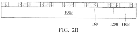
- a second molding compound 120B is formed on the second carrier substrate 100B.
- the second molding compound 120B surrounds the vias 160 and the sidewalls of the second components 110B without covering the top and bottom surfaces of the second components 110B and the vias 160. Namely, the vias 160 penetrate or pass through the second molding compound 120B.
- the second molding compound 120B is formed of a nonconductive material such as an epoxy, a resin, a moldable polymer, or another suitable molding material.
- the second molding compound 120B is applied as a substantial liquid, and then is cured through a chemical reaction.
- the second molding compound 120B is an UV or thermally cured polymer applied as a gel or malleable solid, and then is cured through a UV or thermal curing process. The second molding compound 120B may be cured with a mold.
- the deposited second molding compound 120B covers the top surfaces of the second components 110B and the vias 160, and then a grinding process is performed to thin the deposited second molding compound 120B. As a result, the thinned second molding compound 120B exposes the top surfaces of the second components 110B and the vias 160.
- the top and bottom surfaces of the second molding compound 120B are coplanar with the top and bottom surfaces of the second components 110B, respectively.
- the top and bottom surfaces of the second molding compound 120B are coplanar with the top and bottom surfaces of the vias 160, respectively.
- the second components 110B are previously thinned before being bonded onto the second carrier substrate 100B.
- the second components 110B and the vias 160 substantially have the same thickness and thereby facilitating the exposure of the second components 110B and the vias 160.
- a semiconductor wafer is thinned and is subsequently diced into semiconductor dies (or chips) to form the second components 110B.
- the second components 110B may be thinned by a mechanical grinding process, a chemical mechanical polishing process, a milling process or another suitable process.
- a second RDL structure 130B is formed on the second molding compound 120B and is coupled to the second components 110B and the vias 160.
- a second (semiconductor) package B is formed.
- the second (semiconductor) package B is a wafer-level fan-out package.
- the second RDL structure 130B covers the second molding compound 120B and may be in direct contact with the second molding compound 120B.
- the second RDL structure 130B includes one or more conductive traces 140B disposed in and surrounded by an IMD layer 150B.
- the second components 110B are electrically connected to the conductive traces 140B of the second RDL structure 130B.
- Pad portions of the conductive traces 140B are exposed from the top surface of the second RDL structure 130B.
- the structure of the second RDL structure 130B may be similar to or the same as the structure of the first RDL structure 130A, as aforementioned in detail. It should be noted that the number and configuration of the conductive trace 140B and the IMD layer 150B shown in figures are only examples and are not limitations to the present invention.
- the conductive traces 140B include copper, or another suitable conductive material with good diffusibility.
- FIGS. 3A-3F are cross-sectional views of various stages of a method for forming a semiconductor package assembly, in accordance with some embodiments of the disclosure. Additional operations can be provided before, during, and/or after the stages described in FIGS. 3A-3E . Some of the stages that arc described can be replaced or eliminated for different embodiments. Additional features can be added to the semiconductor package assembly. Some of the features described below can be replaced or eliminated for different embodiments.
- the second package B is bonded to the first package A so that the first RDL structure 130A is sandwiched between the first components 110A and the second RDL structure 130B.
- the conductive traces 140A of the first RDL structure 130A are directly electrically connected to the conductive traces 140B of the second RDL structure 130B.
- the pad portions of the conductive traces 140A and 140B are in direct contact with each other.
- the IMD layer 150A of the first RDL structure 130A and the IMD layer 150B of the second RDL structure 130B are also in direct contact with each other.
- an active surface of the first component 110A faces an active surface of the second component 110B.
- the first package A and the second package B are bonded together using a fusion bonding method.
- the first package A and the second package B are bonded together using a copper fusion bonding method.
- the conductive traces 140A and 140B include copper so that the first package A and the second package B are bonded together through copper joints. The joints between the first package A and the second package B do not include solder.
- the second package B is placed on the first package A.
- the conductive traces 140A directly adjoin the conductive traces 140B.
- the conductive traces 140A substantially align to the conductive traces 140B.
- the conductive traces 140A and the conductive traces 140B have the same layout.
- the conductive traces 140A substantially completely overlap the conductive traces 140B.
- the conductive traces 140A and the conductive traces 140B have different layouts.
- the conductive traces 140A at least partially overlap the conductive traces 140B so as to build electrical connection paths between the first package A and the second package B.
- a thermal treatment is performed over the first package A and the second package B.
- the fusion of metal (copper) in the conductive traces 140A and the conductive traces 140B makes the second package B connect with the first package A.
- the conductive traces 140A directly connect to the conductive traces 140B without a bonding structure (such as a conductive pillar, a conductive bump, or a conductive paste structure).
- the thermal treatment is performed at a temperature that is in a range from about 150 degrees C to about 250 degrees C, but it is not so limited.
- ultrasonic energy is applied to the first package A and the second package B.
- the ultrasonic energy facilitates metal diffusion between the conductive traces 140A and the conductive traces 140B. Therefore, the joints between the first package A and the second package B are strengthened so that the first package A and the second package B are tightly bonded together.
- a planarization process is performed over the first package A and/or the second package B.
- the planarization process is used to reduce surface roughness and provide the first package A and/or the second package B with a flat and even bonding surface.
- the surface of the first RDL structure 130A and/or the second RDL structure 130B has previously been planarized before placing the second package B on the first package A. Therefore, the second package B can be bonded to the first package A intimately.
- the second carrier substrate 100B is removed from the second package B. As a result, the second components 110B and the vias 160 are exposed. The sidewalls of the second components 110B and the vias 160 are still surrounded by the second molding compound 120B.
- the adhesive property of the adhesive layer which is used to bond the second components 110B and the second carrier substrate 100B, is eliminated to debond the second carrier substrate 100B.
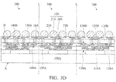
- a conductive component 190 is formed on the second package B away from the first package A.
- the conductive component 190 and the first package A are positioned on two opposite sides of the second package B.
- the second components 110B are positioned between the second RDL structure 130B and the conductive component 190.
- the conductive component 190 is electrically connected or coupled to the second components 110B through the vias 160 and the second RDL structure 130B. In some embodiments, the conductive component 190 is further electrically connected to the first components 110A through the vias 160, the second RDL structure 130B. and the first RDL structure 130A.
- the conductive component 190 is formed of a RDL structure 200 and conductive structures 210 over the RDL structure 200.
- the RDL structure 200 includes one or more conductive traces 220 disposed in and surrounded by an IMD layer 230. Pad portions of the conductive traces 220 are exposed from the top surface of the RDL structure 200.
- the structure of the RDL structure 200 may be similar to or the same as the structure of the first RDL structure 130A, as aforementioned in detail.
- the conductive structures 210 are electrically connected to the exposed pad portions of the conductive traces 220.
- the vias 160 are electrically connected or coupled to the conductive structures 210 through the conductive traces 220.
- the conductive structures 210 are bonding balls (such as solder balls), or another suitable conductive structures. It should be noted that the number and configuration of the conductive structures 210 and the conductive traces 220 shown in figures are only examples and are not limitations to the present invention.
- the conductive component 190 is formed of the conductive structures 210.
- the vias 160 are directly electrically connected to the conductive structures 210.
- the vias 160 may be electrically connected to the conductive structures 210 through one or more conductive layers, such as under bump metallization (UBM) layers.
- UBM under bump metallization
- the first carrier substrate 100A is removed from the first package A. As a result, the first components 110A are exposed. The sidewalls of the first components 110A are still surrounded by the first molding compound 120A.
- the adhesive property of the adhesive layer which is used to bond the first components 110A and the first carrier substrate 100A, is eliminated to debond the first carrier substrate 100A.
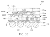
- a singulation process is performed on the bonded packages A and B.
- the bonded packages A and B are cut or diced along scribe lines L to separate the bonded packages A and B into multiple semiconductor package assemblies 300.
- the semiconductor package assemblies 300 are SIP semiconductor package assemblies and wafer-level fan-out packages are integrated in the semiconductor package assemblies 300.
- each of the semiconductor package assemblies 300 includes one first component 110A and two second components 110B.
- the semiconductor package assembly 300 may include more than two second components 110B.
- the size of the First component 110A is different from that of the second components 110B.
- the size of the first component 110A is greater than that of the second components 110B.
- the second components 110B are the same size. In some other embodiments, the second components 110B are different sizes.
- the first component 110A and the second components 110B have the same function. Therefore, the semiconductor package assembly 300 is homogeneous integration. In some other embodiments, the function of the first component 110A is different from the function of one or more of the second components 110B. Therefore, the semiconductor package assembly 300 is heterogeneous integration.
- one of the first component 110A and the second components 110B is a system-on-chip (SOC) and another of the first component 110A and the second components 110B is a passive device.
- one of the first component 110A and the second components 110B is an analog processor (AP) and another of the first component 110A and the second components 110B is a digital processor (DP).
- one of the first component 110A and the second components 110B is a baseband (BB) component and another of the first component 110A and the second components 110B is a radio-frequency (RF) component.
- SOC system-on-chip
- AP analog processor
- DP digital processor
- one of the first component 110A and the second components 110B is a baseband (BB) component and another of the first component 110A and the second components 110B is a radio-frequency (RF) component.
- BB baseband
- RF radio-frequency
- the first component 110A is an active device while the second components 110B are passive devices with the same or different functions.
- the first component 110A and one of the second components 110B are active devices with the same or different functions while another second component 110B is a passive device.
- the first component 110A and the second components 110B are active devices with various different functions.
- the first component 110A is a passive device while the second components 110B are active devices with the same or different functions.
- the first component 110A and one of the second components 110B are passive devices with the same or different functions while another second component 110B is an active device.
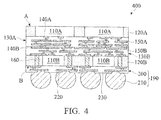
- FIGS. 4 and 5 are cross-sectional views of a semiconductor package assembly, in accordance with some embodiments of the disclosure. Elements in FIGS. 4 and 5 that are the same as those in FIG. 3E are labeled with the same reference numbers as in FIG. 3E and are not described again for brevity.
- a semiconductor package assembly 400 is shown.
- the semiconductor package assembly 400 is similar to the semiconductor package assembly 300 shown in FIG. 3E .
- the main difference between the semiconductor package assemblies 300 and 400 is that the semiconductor package assembly 300 includes one first component 110A while the semiconductor package assembly 400 includes two first components 110A.
- the semiconductor package assembly 400 may include more than two first components 110A.
- the first components 110A are the same size. In some other embodiments, the first components 110A are different sizes. In some embodiments, the size of the first components 110A is different from that of the second components 110B. For example, the size of the first components 110A is greater than that of the second components 110B. In some embodiments, the first components 110A have the same function. In some other embodiments, the first components 110A have the different functions.
- a semiconductor package assembly 500 is shown.
- the semiconductor package assembly 500 is similar to the semiconductor package assembly 300 shown in FIG. 3E .
- the main difference between the semiconductor package assemblies 300 and 500 is that the vias 160 of the semiconductor package assembly 300 are formed in the second package B while the vias 160 of the semiconductor package assembly 500 are formed in the first package A.
- the conductive component 190 of the semiconductor package assembly 300 is formed on the second package B while the conductive component 190 of the semiconductor package assembly 500 is formed on the first package A.
- the vias 160 penetrate the first molding compound 120A and are electrically connected or coupled to the first RDL structure 130A.
- the conductive component 190 and the second package B are positioned on two opposite sides of the first package A.
- the first components 110A are positioned between the first RDL structure 130A and the conductive component 190.
- the semiconductor package assembly and methods for forming the same in accordance with some embodiments of the disclosure provide various advantages. According to the aforementioned embodiments, more than two components or dies can be integrated in a semiconductor package assembly. These components or dies are fabricated in different processes and are known-good components or dies. Therefore, sizes and/or functions of the components or dies are not limited, thereby facilitating improvements to the flexibility of the design. The manufacturing yield of the semiconductor package assembly is significantly enhanced even further.
- two packages are bonded together using a fusion bonding method to form a semiconductor package assembly.
- additional bonding structures such as conductive pillars, conductive bumps, or conductive paste structures
- additional adhesive layer such as conductive pillars, conductive bumps, or conductive paste structures
- the signal transmitting path/distance between the two packages is greatly shortened. Also, the capability of electrical migration (EM) can be further enhanced. In addition, the thickness of the semiconductor package assembly is reduced. Therefore, the device performance of the semiconductor package assembly is significantly improved.
Landscapes
- Engineering & Computer Science (AREA)
- Manufacturing & Machinery (AREA)
- Structures Or Materials For Encapsulating Or Coating Semiconductor Devices Or Solid State Devices (AREA)
- Production Of Multi-Layered Print Wiring Board (AREA)
- Physics & Mathematics (AREA)
- Geometry (AREA)
- Microelectronics & Electronic Packaging (AREA)
Abstract
Description
- This Application claims the benefit of
U.S. Provisional Application No. 62/164,725 filed on May 21, 2015 U.S. Provisional Application No. 62/198,865 filed on July 30, 2015 - The present invention relates to a semiconductor package assembly, and in particular to a three-dimensional (3D) semiconductor package assembly and methods for forming the same.
- The semiconductor industry has experienced continuous and rapid growth due to the desire for miniaturization and multi-functionality of electronic products. Integration density has been improved to allow more chips or dies to be integrated into a semiconductor package, such as a two-dimensional (2D) semiconductor package. However, there are physical limitations to 2D semiconductor packages. For example, when more than two dies with various functions are put into a 2D semiconductor device, it becomes more difficult to develop the more complex designs and layouts that are required.
- Although 3D integrated circuits and stacked dies have been developed and are commonly used, the dies integrated into a conventional 3D semiconductor package are limited to be the same size. Furthermore, 3D semiconductor packaging technology suffers from various problems that may cause a reduction of the manufacturing yield.
- Thus, there exists a need to develop a semiconductor package assembly, and methods for forming the same, capable of mitigating or eliminating the aforementioned problems.
- A semiconductor package assembly and a method for forming a semiconductor package assembly are provided.
- An exemplary embodiment of a semiconductor package assembly includes a first semiconductor package. The first semiconductor package includes a first semiconductor die. A first redistribution layer (RDL) structure is coupled to the first semiconductor die and includes a first conductive trace. The semiconductor package assembly also includes a second semiconductor package bonded to the first semiconductor package. The second semiconductor package includes a second semiconductor die. An active surface of the second semiconductor die faces an active surface of the first semiconductor die. A second RDL structure is coupled to the second semiconductor die and includes a second conductive trace. The first conductive trace is in direct contact with the second conductive trace.
- Another exemplary embodiment of a semiconductor package assembly includes a first package. The first package includes a first component. A first RDL structure is coupled to the first component and includes a first conductive trace. The semiconductor package assembly also includes a second package bonded to the first package. The second package includes a second component. A second RDL structure is coupled to the second component and includes a second conductive trace. The first conductive trace is in direct contact with the second conductive trace.
- An exemplary embodiment of a method for forming a semiconductor package assembly includes forming a first semiconductor package. The first semiconductor package includes a first semiconductor die. A first RDL structure is coupled to the first semiconductor die and includes a first conductive trace. The method also includes forming a second semiconductor package. The second semiconductor package includes a second semiconductor die. An active surface of the second semiconductor die faces an active surface of the first semiconductor die. A second RDL structure is coupled to the second semiconductor die and includes a second conductive trace. The method further includes bonding the second semiconductor package to the first semiconductor package. The first conductive trace is in direct contact with the second conductive trace.
- A detailed description is given in the following embodiments with reference to the accompanying drawings.
- The present invention can be more fully understood by reading the subsequent detailed description and examples with references made to the accompanying drawings, wherein:
-
FIGS. 1A-1C are cross-sectional views of various stages of a method for forming a semiconductor package, in accordance with some embodiments of the disclosure. -
FIGS. 2A-2C are cross-sectional views of various stages of a method for forming a semiconductor package, in accordance with some embodiments of the disclosure. -
FIGS. 3A-3E are cross-sectional views of various stages of a method for forming a semiconductor package assembly, in accordance with some embodiments of the disclosure. -
FIG. 4 is a cross-sectional view of a semiconductor package assembly, in accordance with some embodiments of the disclosure. -
FIG. 5 is a cross-sectional view of a semiconductor package assembly, in accordance with some embodiments of the disclosure. - The following description is of the best-contemplated mode of carrying out the invention. This description is made for the purpose of illustrating the general principles of the invention and should not be taken in a limiting sense. The scope of the invention is determined by reference to the appended claims.
- The present invention will be described with respect to particular embodiments and with reference to certain drawings, but the invention is not limited thereto and is only limited by the claims. The drawings described are only schematic and are non-limiting. In the drawings, the size of some of the elements may be exaggerated for illustrative purposes and not drawn to scale. The dimensions and the relative dimensions do not correspond to actual dimensions in the practice of the invention.
- Embodiments of the disclosure provide a 3D system-in-package (SIP) semiconductor package assembly. The semiconductor package assembly is integrated with more than two components or dies so that the size of electronic products made using the semiconductor package assembly can be reduced. These components or dies are separately fabricated and are subsequently integrated into the semiconductor package assembly. As a result, their sizes and/or functions are not limited to be the same. The design flexibility of the semiconductor package assembly is greatly improved. Furthermore, these components or dies are tested in advance to make sure that the semiconductor package assembly only includes good components or dies. As a result, the yield loss resulted from multiple defective components or dies is significantly mitigated or eliminated. Therefore, the manufacturing cost of the semiconductor package assembly is reduced.
-
FIGS. 1A-1C are cross-sectional views of various stages of a method for forming a semiconductor package, in accordance with some embodiments of the disclosure. Additional operations can be provided before, during, and/or after the stages described inFIGS. 1A-1C . Some of the stages that are described can be replaced or eliminated for different embodiments. Additional features can be added to the semiconductor package. Some of the features described below can be replaced or eliminated for different embodiments. - As shown in
FIG. 1A , afirst carrier substrate 100A is provided. In some embodiments, thefirst carrier substrate 100A is a wafer or a panel. Thefirst carrier substrate 100A may include glass or another suitable supporting material. - As shown in
FIG. 1A , multiplefirst components 110A are bonded onto thefirst carrier substrate 100A. In accordance with some embodiments of the disclosure, thefirst components 110A are known-good components. In other words, no defective components are bonded onto thefirst carrier substrate 100A. In some embodiments, thefirst components 110A and thefirst carrier substrate 100A are attached together through an adhesive layer such as glue or another suitable adhesive material. - In some embodiments, the
first components 110A are active devices and can be referred to as first semiconductor dies (or chips) 110A. The first semiconductor dies 110A may include transistors or another suitable active element. For example, the first semiconductor dies 110A may be a logic die including a central processing unit (CPU), a graphics processing unit (GPU), a dynamic random access memory (DRAM) controller or any combination thereof. In some other embodiments, thefirst components 110A are passive devices such as integrated passive devices (IPDs). Thefirst components 110A may include capacitors, resistors, inductors, varactor diodes or another suitable passive element. - As shown in
FIG. 1B , afirst molding compound 120A is formed on thefirst carrier substrate 100A. Thefirst molding compound 120A surrounds the sidewalls of thefirst components 110A without covering the top and bottom surfaces of thefirst components 110A. - In some embodiments, the
first molding compound 120A is formed of a nonconductive material such as an epoxy, a resin, a moldable polymer, or another suitable molding material. In some embodiments, thefirst molding compound 120A is applied as a substantial liquid, and then is cured through a chemical reaction. In some other embodiments, thefirst molding compound 120A is an ultraviolet (UV) or thermally cured polymer applied as a gel or malleable solid, and then is cured through a UV or thermal curing process. Thefirst molding compound 120A may be cured with a mold. - In some embodiments, the deposited
first molding compound 120A covers the top surfaces of thefirst components 110A, and then a grinding process is performed to thin the depositedfirst molding compound 120A. As a result, the thinnedfirst molding compound 120A exposes the top surfaces of thefirst components 110A. In some embodiments, the top and bottom surfaces of thefirst molding compound 120A are coplanar with the top and bottom surfaces of thefirst components 110A, respectively. - As shown in
FIG. 1C , a first redistribution layer (RDL)structure 130A, which is also referred to as a fan-out structure, is formed on thefirst molding compound 120A and is coupled to thefirst components 110A. As a result, a first (semiconductor) package A is formed. In some embodiments, the first (semiconductor) package A is a wafer-level fan-out package. - The
first RDL structure 130A covers thefirst molding compound 120A and may be in direct contact with thefirst molding compound 120A. In some embodiments, thefirst RDL structure 130A includes one or moreconductive traces 140A disposed in and surrounded by an inter-metal dielectric (IMD)layer 150A. Thefirst components 110A are electrically connected to theconductive traces 140A of thefirst RDL structure 130A. TheIMD layer 150A may include multiple sub-dielectric layers successively stacked on thefirst molding compound 120A and thefirst components 110A. For example, a first layer-level of theconductive traces 140A is positioned on a first layer-level of the sub-dielectric layers and covered by a second layer-level of the sub-dielectric layers. A second layer-level of theconductive traces 140A is positioned on the second layer-level of the sub-dielectric layers and covered by a third layer-level of the sub-dielectric layers. - In some embodiments, the
IMD layer 150A may be formed of organic materials, which include a polymer base material, non-organic materials, which include silicon nitride (SiNX), silicon oxide (SiOX), graphene, or the like. In some embodiments, theIMD layer 150A is a high-k dielectric layer (k is the dielectric constant of the dielectric layer). In some other embodiments, theIMD layer 150A may be formed of a photosensitive material, which includes a dry film photoresist, or a taping film. - Pad portions of the
conductive traces 140A are exposed from the top surface of thefirst RDL structure 130A. For example, the pad portions of theconductive traces 140A are exposed from openings of theIMD layer 150A and connected to subsequently formed conductive components. It should be noted that the number and configuration of theconductive trace 140A and theIMD layer 150A shown in figures are only examples and are not limitations to the present invention. In some embodiments, the conductive traces 140A include copper, or another suitable conductive material with good diffusibility. -
FIGS. 2A-2C are cross-sectional views of various stages of a method for forming a semiconductor package, in accordance with some embodiments of the disclosure. Additional operations can be provided before, during, and/or after the stages described inFIGS. 2A-2C . Some of the stages that are described can be replaced or eliminated for different embodiments. Additional features can be added to the semiconductor package. Some of the features described below can be replaced or eliminated for different embodiments. - As shown in
FIG. 2A , asecond carrier substrate 100B is provided. In some embodiments, thesecond carrier substrate 100B is a wafer or a panel. Thesecond carrier substrate 100B may include glass, or another suitable supporting material. - As shown in
FIG. 2A ,multiple vias 160 are formed on thesecond carrier substrate 100B. Thevias 160 may be through interposer vias (TIV). In some embodiments, thevias 160 are copper pillars or other suitable conductive structures. In some embodiments, thevias 160 are formed by an electroplating process or another suitable process. - As shown in
FIG. 2A , multiplesecond components 110B are bonded onto thesecond carrier substrate 100B. In accordance with some embodiments of the disclosure, thesecond components 110B are known-good components. In other words, no defective components are bonded onto thesecond carrier substrate 100B. In some embodiments, thesecond components 110B and thesecond carrier substrate 100B are attached together through an adhesive layer such as glue or another suitable adhesive material. In some embodiments, each of thesecond components 110B is positioned between two of thevias 160. In some embodiments, one ormore vias 160 are positioned between two of thesecond components 110B. - In some embodiments, the
second components 110B are active devices and can be referred to as second semiconductor dies (or chips) 110B. The second semiconductor dies 110B may include transistors or other suitable active elements. For example, the second semiconductor dies 110B may be a logic die including a CPU, a GPU, a DRAM controller or any combination thereof. In some other embodiments, thesecond components 110B are passive devices such as IPDs. Thesecond components 110B may include capacitors, resistors, inductors, varactor diodes, and other suitable passive elements. - As shown in
FIG. 2B , asecond molding compound 120B is formed on thesecond carrier substrate 100B. Thesecond molding compound 120B surrounds thevias 160 and the sidewalls of thesecond components 110B without covering the top and bottom surfaces of thesecond components 110B and thevias 160. Namely, thevias 160 penetrate or pass through thesecond molding compound 120B. - In some embodiments, the
second molding compound 120B is formed of a nonconductive material such as an epoxy, a resin, a moldable polymer, or another suitable molding material. In some embodiments, thesecond molding compound 120B is applied as a substantial liquid, and then is cured through a chemical reaction. In some other embodiments, thesecond molding compound 120B is an UV or thermally cured polymer applied as a gel or malleable solid, and then is cured through a UV or thermal curing process. Thesecond molding compound 120B may be cured with a mold. - In some embodiments, the deposited
second molding compound 120B covers the top surfaces of thesecond components 110B and thevias 160, and then a grinding process is performed to thin the depositedsecond molding compound 120B. As a result, the thinnedsecond molding compound 120B exposes the top surfaces of thesecond components 110B and thevias 160. In some embodiments, the top and bottom surfaces of thesecond molding compound 120B are coplanar with the top and bottom surfaces of thesecond components 110B, respectively. In some embodiments, the top and bottom surfaces of thesecond molding compound 120B are coplanar with the top and bottom surfaces of thevias 160, respectively. - In accordance with some embodiments of the disclosure, the
second components 110B are previously thinned before being bonded onto thesecond carrier substrate 100B. As a result, thesecond components 110B and thevias 160 substantially have the same thickness and thereby facilitating the exposure of thesecond components 110B and thevias 160. For example, a semiconductor wafer is thinned and is subsequently diced into semiconductor dies (or chips) to form thesecond components 110B. Thesecond components 110B may be thinned by a mechanical grinding process, a chemical mechanical polishing process, a milling process or another suitable process. - As shown in
FIG. 2C , asecond RDL structure 130B is formed on thesecond molding compound 120B and is coupled to thesecond components 110B and thevias 160. As a result, a second (semiconductor) package B is formed. In some embodiments, the second (semiconductor) package B is a wafer-level fan-out package. Thesecond RDL structure 130B covers thesecond molding compound 120B and may be in direct contact with thesecond molding compound 120B. In some embodiments, thesecond RDL structure 130B includes one or moreconductive traces 140B disposed in and surrounded by anIMD layer 150B. Thesecond components 110B are electrically connected to the conductive traces 140B of thesecond RDL structure 130B. Pad portions of the conductive traces 140B are exposed from the top surface of thesecond RDL structure 130B. The structure of thesecond RDL structure 130B may be similar to or the same as the structure of thefirst RDL structure 130A, as aforementioned in detail. It should be noted that the number and configuration of theconductive trace 140B and theIMD layer 150B shown in figures are only examples and are not limitations to the present invention. In some embodiments, the conductive traces 140B include copper, or another suitable conductive material with good diffusibility. -
FIGS. 3A-3F are cross-sectional views of various stages of a method for forming a semiconductor package assembly, in accordance with some embodiments of the disclosure. Additional operations can be provided before, during, and/or after the stages described inFIGS. 3A-3E . Some of the stages that arc described can be replaced or eliminated for different embodiments. Additional features can be added to the semiconductor package assembly. Some of the features described below can be replaced or eliminated for different embodiments. - As shown in
FIG. 3A , the second package B is bonded to the first package A so that thefirst RDL structure 130A is sandwiched between thefirst components 110A and thesecond RDL structure 130B. The conductive traces 140A of thefirst RDL structure 130A are directly electrically connected to the conductive traces 140B of thesecond RDL structure 130B. For example, the pad portions of theconductive traces IMD layer 150A of thefirst RDL structure 130A and theIMD layer 150B of thesecond RDL structure 130B are also in direct contact with each other. In some embodiments, an active surface of thefirst component 110A faces an active surface of thesecond component 110B. - In accordance with some embodiments of the disclosure, the first package A and the second package B are bonded together using a fusion bonding method. In some embodiments, the first package A and the second package B are bonded together using a copper fusion bonding method. For example, the
conductive traces - The second package B is placed on the first package A. The conductive traces 140A directly adjoin the conductive traces 140B. In some embodiments, the conductive traces 140A substantially align to the conductive traces 140B. In some embodiments, the
conductive traces 140A and the conductive traces 140B have the same layout. The conductive traces 140A substantially completely overlap the conductive traces 140B. In some other embodiments, theconductive traces 140A and the conductive traces 140B have different layouts. The conductive traces 140A at least partially overlap the conductive traces 140B so as to build electrical connection paths between the first package A and the second package B. - Afterwards, a thermal treatment is performed over the first package A and the second package B. As a result, the fusion of metal (copper) in the
conductive traces 140A and theconductive traces 140B makes the second package B connect with the first package A. The conductive traces 140A directly connect to the conductive traces 140B without a bonding structure (such as a conductive pillar, a conductive bump, or a conductive paste structure). In some embodiments, the thermal treatment is performed at a temperature that is in a range from about 150 degrees C to about 250 degrees C, but it is not so limited. - In some embodiments, during the thermal treatment, ultrasonic energy is applied to the first package A and the second package B. The ultrasonic energy facilitates metal diffusion between the
conductive traces 140A and the conductive traces 140B. Therefore, the joints between the first package A and the second package B are strengthened so that the first package A and the second package B are tightly bonded together. - In some embodiments, before placing the second package B on the first package A, a planarization process is performed over the first package A and/or the second package B. The planarization process is used to reduce surface roughness and provide the first package A and/or the second package B with a flat and even bonding surface. For example, the surface of the
first RDL structure 130A and/or thesecond RDL structure 130B has previously been planarized before placing the second package B on the first package A. Therefore, the second package B can be bonded to the first package A intimately. - As shown in
FIG. 3B , thesecond carrier substrate 100B is removed from the second package B. As a result, thesecond components 110B and thevias 160 are exposed. The sidewalls of thesecond components 110B and thevias 160 are still surrounded by thesecond molding compound 120B. In some embodiments, the adhesive property of the adhesive layer, which is used to bond thesecond components 110B and thesecond carrier substrate 100B, is eliminated to debond thesecond carrier substrate 100B. - As shown in
FIG. 3C , aconductive component 190 is formed on the second package B away from the first package A. In other words, theconductive component 190 and the first package A are positioned on two opposite sides of the second package B. Thesecond components 110B are positioned between thesecond RDL structure 130B and theconductive component 190. - In some embodiments, the
conductive component 190 is electrically connected or coupled to thesecond components 110B through thevias 160 and thesecond RDL structure 130B. In some embodiments, theconductive component 190 is further electrically connected to thefirst components 110A through thevias 160, the second RDL structure 130B. and thefirst RDL structure 130A. - In some embodiments, the
conductive component 190 is formed of aRDL structure 200 andconductive structures 210 over theRDL structure 200. In some embodiments, theRDL structure 200 includes one or moreconductive traces 220 disposed in and surrounded by anIMD layer 230. Pad portions of theconductive traces 220 are exposed from the top surface of theRDL structure 200. The structure of theRDL structure 200 may be similar to or the same as the structure of thefirst RDL structure 130A, as aforementioned in detail. - The
conductive structures 210 are electrically connected to the exposed pad portions of the conductive traces 220. Thevias 160 are electrically connected or coupled to theconductive structures 210 through the conductive traces 220. In some embodiments, theconductive structures 210 are bonding balls (such as solder balls), or another suitable conductive structures. It should be noted that the number and configuration of theconductive structures 210 and theconductive traces 220 shown in figures are only examples and are not limitations to the present invention. - In some other embodiments, the
conductive component 190 is formed of theconductive structures 210. Thevias 160 are directly electrically connected to theconductive structures 210. Thevias 160 may be electrically connected to theconductive structures 210 through one or more conductive layers, such as under bump metallization (UBM) layers. - As shown in
FIG. 3D , thefirst carrier substrate 100A is removed from the first package A. As a result, thefirst components 110A are exposed. The sidewalls of thefirst components 110A are still surrounded by thefirst molding compound 120A. In some embodiments, the adhesive property of the adhesive layer, which is used to bond thefirst components 110A and thefirst carrier substrate 100A, is eliminated to debond thefirst carrier substrate 100A. - Afterwards, a singulation process is performed on the bonded packages A and B. The bonded packages A and B are cut or diced along scribe lines L to separate the bonded packages A and B into multiple
semiconductor package assemblies 300. Thesemiconductor package assemblies 300 are SIP semiconductor package assemblies and wafer-level fan-out packages are integrated in thesemiconductor package assemblies 300. - As shown in
FIG. 3E , each of thesemiconductor package assemblies 300 includes onefirst component 110A and twosecond components 110B. Thesemiconductor package assembly 300 may include more than twosecond components 110B. In some embodiments, the size of theFirst component 110A is different from that of thesecond components 110B. For example, the size of thefirst component 110A is greater than that of thesecond components 110B. In some embodiments, thesecond components 110B are the same size. In some other embodiments, thesecond components 110B are different sizes. - In some embodiments, the
first component 110A and thesecond components 110B have the same function. Therefore, thesemiconductor package assembly 300 is homogeneous integration. In some other embodiments, the function of thefirst component 110A is different from the function of one or more of thesecond components 110B. Therefore, thesemiconductor package assembly 300 is heterogeneous integration. - In some embodiments, one of the
first component 110A and thesecond components 110B is a system-on-chip (SOC) and another of thefirst component 110A and thesecond components 110B is a passive device. In some embodiments, one of thefirst component 110A and thesecond components 110B is an analog processor (AP) and another of thefirst component 110A and thesecond components 110B is a digital processor (DP). In some embodiments, one of thefirst component 110A and thesecond components 110B is a baseband (BB) component and another of thefirst component 110A and thesecond components 110B is a radio-frequency (RF) component. - For example, in some embodiments, the
first component 110A is an active device while thesecond components 110B are passive devices with the same or different functions. In some embodiments, thefirst component 110A and one of thesecond components 110B are active devices with the same or different functions while anothersecond component 110B is a passive device. In some other embodiments, thefirst component 110A and thesecond components 110B are active devices with various different functions. - Alternatively, in some embodiments, the
first component 110A is a passive device while thesecond components 110B are active devices with the same or different functions. In some embodiments, thefirst component 110A and one of thesecond components 110B are passive devices with the same or different functions while anothersecond component 110B is an active device. - Many variations and/or modifications can be made to embodiments of the disclosure.
FIGS. 4 and5 are cross-sectional views of a semiconductor package assembly, in accordance with some embodiments of the disclosure. Elements inFIGS. 4 and5 that are the same as those inFIG. 3E are labeled with the same reference numbers as inFIG. 3E and are not described again for brevity. - Referring to
FIG. 4 . asemiconductor package assembly 400 is shown. Thesemiconductor package assembly 400 is similar to thesemiconductor package assembly 300 shown inFIG. 3E . The main difference between thesemiconductor package assemblies semiconductor package assembly 300 includes onefirst component 110A while thesemiconductor package assembly 400 includes twofirst components 110A. Thesemiconductor package assembly 400 may include more than twofirst components 110A. - In some embodiments, the
first components 110A are the same size. In some other embodiments, thefirst components 110A are different sizes. In some embodiments, the size of thefirst components 110A is different from that of thesecond components 110B. For example, the size of thefirst components 110A is greater than that of thesecond components 110B. In some embodiments, thefirst components 110A have the same function. In some other embodiments, thefirst components 110A have the different functions. - Referring to
FIG. 5 , asemiconductor package assembly 500 is shown. Thesemiconductor package assembly 500 is similar to thesemiconductor package assembly 300 shown inFIG. 3E . The main difference between thesemiconductor package assemblies vias 160 of thesemiconductor package assembly 300 are formed in the second package B while thevias 160 of thesemiconductor package assembly 500 are formed in the first package A. As a result, theconductive component 190 of thesemiconductor package assembly 300 is formed on the second package B while theconductive component 190 of thesemiconductor package assembly 500 is formed on the first package A. - In
FIG. 5 , thevias 160 penetrate thefirst molding compound 120A and are electrically connected or coupled to thefirst RDL structure 130A. Theconductive component 190 and the second package B are positioned on two opposite sides of the first package A. Thefirst components 110A are positioned between thefirst RDL structure 130A and theconductive component 190. - The semiconductor package assembly and methods for forming the same in accordance with some embodiments of the disclosure provide various advantages. According to the aforementioned embodiments, more than two components or dies can be integrated in a semiconductor package assembly. These components or dies are fabricated in different processes and are known-good components or dies. Therefore, sizes and/or functions of the components or dies are not limited, thereby facilitating improvements to the flexibility of the design. The manufacturing yield of the semiconductor package assembly is significantly enhanced even further.
- Furthermore, according to the aforementioned embodiments, two packages are bonded together using a fusion bonding method to form a semiconductor package assembly. There is no need to form additional bonding structures (such as conductive pillars, conductive bumps, or conductive paste structures) or an additional adhesive layer. Accordingly, the process flow of the semiconductor package assembly is simplified and the manufacturing cost is reduced.
- Since the two packages are directly bonded without any intervening layer, the signal transmitting path/distance between the two packages is greatly shortened. Also, the capability of electrical migration (EM) can be further enhanced. In addition, the thickness of the semiconductor package assembly is reduced. Therefore, the device performance of the semiconductor package assembly is significantly improved.
- While the invention has been described by way of example and in terms of the preferred embodiments, it should be understood that the invention is not limited to the disclosed embodiments. On the contrary, it is intended to cover various modifications and similar arrangements (as would be apparent to those skilled in the art). Therefore, the scope of the appended claims should be accorded the broadest interpretation so as to encompass all such modifications and similar arrangements.
Claims (15)
- A semiconductor package assembly, comprising:a first semiconductor package, comprising:a first semiconductor die; anda first redistribution layer (RDL) structure coupled to the first semiconductor die and comprising a first conductive trace; anda second semiconductor package bonded to the first semiconductor package, wherein the second semiconductor package comprises:a second semiconductor die, wherein an active surface of the second semiconductor die faces an active surface of the first semiconductor die; anda second RDL structure coupled to the second semiconductor die and comprising a second conductive trace, wherein the first conductive trace is in direct contact with the second conductive trace.
- The semiconductor package assembly as claimed in claim 1, wherein the first semiconductor package comprises more than one first semiconductor die or the second semiconductor package comprises more than one second semiconductor die.
- The semiconductor package assembly as claimed in claim 1 or 2, wherein the first conductive trace and the second conductive trace comprise copper,
wherein preferably, the first RDL structure further comprises a first dielectric layer surrounding the first conductive trace, and the second RDL structure further comprises a second dielectric layer surrounding the second conductive trace and in direct contact with the second dielectric layer. - The semiconductor package assembly as claimed in one of the precedings claims, wherein the first semiconductor die and the second semiconductor die are different sizes.
- The semiconductor package assembly as claimed in one of the preceding claims, wherein the first semiconductor package further comprises a first molding compound, wherein the first molding compound surrounds sidewalls of the first semiconductor die.
- The semiconductor package assembly as claimed in claim 5, wherein the first RDL structure covers the first molding compound, and/or
wherein the first semiconductor package further comprises a via, wherein the via penetrates the first molding compound and is coupled to the first RDL structure, wherein the semiconductor package assembly preferably further comprises a conductive component coupled to the via, wherein the first semiconductor die is positioned between the first RDL structure and the conductive component. - The semiconductor package assembly as claimed in one of the preceding claims, wherein the second semiconductor package further comprises a second molding compound, and the second molding compound surrounds sidewalls of the second semiconductor die.
- The semiconductor package assembly as claimed in claim 7, wherein the second RDL structure covers the second molding compound.
- The semiconductor package assembly as claimed in claim 7 or 8, wherein the second semiconductor package further comprises a via, wherein the via penetrates the second molding compound and is coupled to the second RDL structure, wherein
the semiconductor package preferably further comprises a conductive component coupled to the via, wherein the second semiconductor die is positioned between the second RDL structure and the conductive component. - A method for forming a semiconductor package assembly, comprising:forming a first semiconductor package, wherein the first semiconductor package comprises:a first semiconductor die; anda first redistribution layer (RDL) structure coupled to the first semiconductor die and comprising a first conductive trace;forming a second semiconductor package, wherein the second semiconductor package comprises:a second semiconductor die, wherein an active surface of the second semiconductor die faces an active surface of the first semiconductor die; anda second RDL structure coupled to the second semiconductor die and comprising a second conductive trace; andbonding the second semiconductor package to the first semiconductor package, wherein the first conductive trace is in direct contact with the second conductive trace.
- The method as claimed in claim 10, wherein the second semiconductor package is bonded to the first semiconductor package using a fusion bonding method, wherein the method preferably
further comprises applying ultrasonic energy during the bonding of the second semiconductor package to the first semiconductor package. - The method as claimed in claim 10 or 11, wherein the formation of the second semiconductor package comprises:forming vias on a second carrier substrate;bonding the second semiconductor die onto the second carrier substrate;forming a second molding compound on the second carrier substrate, wherein the second molding compound surrounds the vias and sidewalls of the second semiconductor die, and wherein the second molding compound exposes top surfaces of the vias and the second semiconductor die; andforming the second RDL structure on the second semiconductor die and the second molding compound.
- The method as claimed in claim 12, further comprising removing the second carrier substrate after bonding the second semiconductor package to the first semiconductor package, wherein the method preferably
further comprises forming a conductive component on the second semiconductor package after removing the second carrier substrate. - The method as claimed in one of claims 10 to 13, wherein the formation of the first semiconductor package comprises:bonding the first semiconductor die onto a first carrier substrate;forming a first molding compound on the first carrier substrate, wherein the first molding compound surrounds sidewalls of the first semiconductor die and exposes a top surface of the first semiconductor die; andforming the first RDL structure on the first semiconductor die and the first molding compound.
- The method as claimed in claim 14, further comprising:removing the first carrier substrate after bonding the second semiconductor package to the first semiconductor package; andperforming a singulation process to the first semiconductor package and the second semiconductor package, and/orwherein the formation of the first semiconductor package comprises bonding more than one first semiconductor die onto the first carrier substrate, wherein the first molding compound further surrounds sidewalls of the first semiconductor dies and exposes a top surface of the first semiconductor dies.
Applications Claiming Priority (3)
| Application Number | Priority Date | Filing Date | Title |
|---|---|---|---|
| US201562164725P | 2015-05-21 | 2015-05-21 | |
| US201562198865P | 2015-07-30 | 2015-07-30 | |
| US15/071,573 US10032756B2 (en) | 2015-05-21 | 2016-03-16 | Semiconductor package assembly with facing active surfaces of first and second semiconductor die and method for forming the same |
Publications (2)
| Publication Number | Publication Date |
|---|---|
| EP3096350A1 true EP3096350A1 (en) | 2016-11-23 |
| EP3096350B1 EP3096350B1 (en) | 2021-08-11 |
Family
ID=55809003
Family Applications (1)
| Application Number | Title | Priority Date | Filing Date |
|---|---|---|---|
| EP16166762.1A Active EP3096350B1 (en) | 2015-05-21 | 2016-04-24 | Semiconductor package assembly and method for forming the same |
Country Status (4)
| Country | Link |
|---|---|
| US (1) | US10032756B2 (en) |
| EP (1) | EP3096350B1 (en) |
| CN (1) | CN106169459A (en) |
| TW (1) | TWI578460B (en) |
Cited By (2)
| Publication number | Priority date | Publication date | Assignee | Title |
|---|---|---|---|---|
| US20170365565A1 (en) * | 2016-06-15 | 2017-12-21 | Broadcom Corporation | High density redistribution layer (rdl) interconnect bridge using a reconstituted wafer |
| WO2021086864A1 (en) * | 2019-11-01 | 2021-05-06 | Xilinx, Inc. | Multi-chip stacked devices |
Families Citing this family (38)
| Publication number | Priority date | Publication date | Assignee | Title |
|---|---|---|---|---|
| KR101731700B1 (en) | 2015-03-18 | 2017-04-28 | 앰코 테크놀로지 코리아 주식회사 | Semiconductor device and manufacturing method thereof |
| US9881902B2 (en) * | 2015-08-05 | 2018-01-30 | Mediatek Inc. | Semiconductor package, semiconductor device using the same and manufacturing method thereof |
| TWI628757B (en) * | 2015-12-23 | 2018-07-01 | 力成科技股份有限公司 | Ultimate thin fan-out type chip package structure and manufacturing method thereof |
| US10204893B2 (en) | 2016-05-19 | 2019-02-12 | Invensas Bonding Technologies, Inc. | Stacked dies and methods for forming bonded structures |
| US10032702B2 (en) * | 2016-12-09 | 2018-07-24 | Dyi-chung Hu | Package structure and manufacturing method thereof |
| TWI643305B (en) * | 2017-01-16 | 2018-12-01 | Powertech Technology Inc. | Package structure and manufacturing method thereof |
| US10217720B2 (en) * | 2017-06-15 | 2019-02-26 | Invensas Corporation | Multi-chip modules formed using wafer-level processing of a reconstitute wafer |
| KR101922884B1 (en) | 2017-10-26 | 2018-11-28 | 삼성전기 주식회사 | Fan-out semiconductor package |
| CN107818958B (en) * | 2017-11-20 | 2023-10-13 | 长鑫存储技术有限公司 | Bottom packaging structure and manufacturing method |
| US20210375814A1 (en) * | 2017-12-06 | 2021-12-02 | Anhui Yunta Electronic Technologies Co., Ltd. | Integrated circuit module structure and method for manufacturing same |
| CN107845614A (en) * | 2017-12-06 | 2018-03-27 | 安徽云塔电子科技有限公司 | A kind of integrated circuit module structure and preparation method thereof |
| US10665522B2 (en) * | 2017-12-22 | 2020-05-26 | Intel IP Corporation | Package including an integrated routing layer and a molded routing layer |
| CN110071073B (en) * | 2018-01-22 | 2022-03-22 | 江苏长电科技股份有限公司 | Package structure and preparation method thereof |
| KR102491103B1 (en) * | 2018-02-06 | 2023-01-20 | 삼성전자주식회사 | Semiconductor package and method of fabricating the same |
| US11735570B2 (en) | 2018-04-04 | 2023-08-22 | Intel Corporation | Fan out packaging pop mechanical attach method |
| US11276676B2 (en) | 2018-05-15 | 2022-03-15 | Invensas Bonding Technologies, Inc. | Stacked devices and methods of fabrication |
| WO2020010136A1 (en) | 2018-07-06 | 2020-01-09 | Invensas Bonding Technologies, Inc. | Molded direct bonded and interconnected stack |
| WO2020010265A1 (en) | 2018-07-06 | 2020-01-09 | Invensas Bonding Technologies, Inc. | Microelectronic assemblies |
| US20200118940A1 (en) * | 2018-10-15 | 2020-04-16 | Intel Corporation | Die with bumper for solder joint reliability |
| CN113330557A (en) | 2019-01-14 | 2021-08-31 | 伊文萨思粘合技术公司 | Bonding structure |
| US11239173B2 (en) | 2019-03-28 | 2022-02-01 | Taiwan Semiconductor Manufacturing Co., Ltd. | Structure and formation method of chip package with fan-out feature |
| WO2020232678A1 (en) * | 2019-05-22 | 2020-11-26 | 华为技术有限公司 | Method for manufacturing 3dic chip and 3dic chip |
| US11296053B2 (en) | 2019-06-26 | 2022-04-05 | Invensas Bonding Technologies, Inc. | Direct bonded stack structures for increased reliability and improved yield in microelectronics |
| KR102661671B1 (en) | 2019-07-25 | 2024-04-29 | 삼성전자주식회사 | Semiconductor package having stacked semiconductor chips |
| US11244879B2 (en) * | 2019-09-26 | 2022-02-08 | Taiwan Semiconductor Manufacturing Company, Ltd. | Semiconductor package |
| TWI720847B (en) | 2020-03-17 | 2021-03-01 | 欣興電子股份有限公司 | Chip package structure and manufacturing method thereof |
| KR102937947B1 (en) * | 2020-05-18 | 2026-03-10 | 삼성전자주식회사 | Semiconductor package |
| US11631647B2 (en) | 2020-06-30 | 2023-04-18 | Adeia Semiconductor Bonding Technologies Inc. | Integrated device packages with integrated device die and dummy element |
| US11417582B2 (en) * | 2020-08-30 | 2022-08-16 | Taiwan Semiconductor Manufacturing Company, Ltd. | Package structure and method of manufacturing the same |
| US11728273B2 (en) | 2020-09-04 | 2023-08-15 | Adeia Semiconductor Bonding Technologies Inc. | Bonded structure with interconnect structure |
| US11764177B2 (en) | 2020-09-04 | 2023-09-19 | Adeia Semiconductor Bonding Technologies Inc. | Bonded structure with interconnect structure |
| US12125775B2 (en) * | 2020-11-11 | 2024-10-22 | Nepes Co., Ltd. | Semiconductor package and method for manufacturing the same |
| US12588482B2 (en) * | 2022-02-14 | 2026-03-24 | Taiwan Semiconductor Manufacturing Co., Ltd. | Method for forming semiconductor redistribution structures |
| TWI807827B (en) * | 2022-05-13 | 2023-07-01 | 矽品精密工業股份有限公司 | Electronic packaging and manufacturing method thereof |
| KR20240007498A (en) | 2022-07-08 | 2024-01-16 | 삼성전자주식회사 | Semiconductor package |
| US20240055343A1 (en) * | 2022-08-12 | 2024-02-15 | Ap Memory Technology Corporation | Semiconductor package structure |
| CN115312470B (en) * | 2022-09-06 | 2025-10-24 | 上海美维科技有限公司 | Stacked packaging structure based on organic carrier and RDL and its preparation method |
| CN115799086A (en) * | 2022-12-09 | 2023-03-14 | 成都海光集成电路设计有限公司 | Chip Packaging Method |
Citations (7)
| Publication number | Priority date | Publication date | Assignee | Title |
|---|---|---|---|---|
| US20080237883A1 (en) * | 2007-03-30 | 2008-10-02 | Nec Corporation | Semiconductor device and method of manufacturing the same |
| JP2010219477A (en) * | 2009-03-19 | 2010-09-30 | Shinko Electric Ind Co Ltd | Method of wiring substrate with electronic component incorporated therein |
| US20110037169A1 (en) * | 2009-08-12 | 2011-02-17 | Stats Chippac, Ltd. | Semiconductor Device and Method of Dual-Molding Die Formed on Opposite Sides of Build-Up Interconnect Structures |
| US20130037950A1 (en) * | 2011-08-10 | 2013-02-14 | Taiwan Semiconductor Manufacturing Company, Ltd. | Multi-Chip Wafer Level Package |
| FR2980036A1 (en) * | 2011-09-12 | 2013-03-15 | St Microelectronics Crolles 2 | Method for realizing three-dimensional integrated structure, involves realizing electrically conductive through-connection extending between non-assembled face and metal line of interconnection part of one of two integrated circuits |
| US8455936B2 (en) * | 2010-02-25 | 2013-06-04 | Avago Technologies General Ip (Singapore) Pte. Ltd. | Configurable memory sheet and package assembly |
| US20140252647A1 (en) * | 2013-03-08 | 2014-09-11 | Taiwan Semiconductor Manufacturing Company, Ltd. | Warpage Reduction and Adhesion Improvement of Semiconductor Die Package |
Family Cites Families (10)
| Publication number | Priority date | Publication date | Assignee | Title |
|---|---|---|---|---|
| US7842948B2 (en) * | 2004-02-27 | 2010-11-30 | Nvidia Corporation | Flip chip semiconductor die internal signal access system and method |
| WO2007126090A1 (en) | 2006-04-27 | 2007-11-08 | Nec Corporation | Circuit board, electronic device and method for manufacturing circuit board |
| JP2010238898A (en) | 2009-03-31 | 2010-10-21 | Toshiba Corp | Semiconductor device |
| TWI402941B (en) * | 2009-12-03 | 2013-07-21 | 日月光半導體製造股份有限公司 | Semiconductor structure and method for making the same |
| US8169065B2 (en) | 2009-12-22 | 2012-05-01 | Epic Technologies, Inc. | Stackable circuit structures and methods of fabrication thereof |
| US8674513B2 (en) * | 2010-05-13 | 2014-03-18 | Taiwan Semiconductor Manufacturing Company, Ltd. | Interconnect structures for substrate |
| US8970023B2 (en) | 2013-02-04 | 2015-03-03 | Taiwan Semiconductor Manufacturing Company, Ltd. | Package structure and methods of forming same |
| KR102053349B1 (en) * | 2013-05-16 | 2019-12-06 | 삼성전자주식회사 | Semiconductor package |
| CN104505382A (en) | 2014-12-30 | 2015-04-08 | 华天科技(西安)有限公司 | Wafer-level fan-out PoP encapsulation structure and making method thereof |
| US9613931B2 (en) * | 2015-04-30 | 2017-04-04 | Taiwan Semiconductor Manufacturing Company, Ltd. | Fan-out stacked system in package (SIP) having dummy dies and methods of making the same |
-
2016
- 2016-03-16 US US15/071,573 patent/US10032756B2/en active Active
- 2016-04-24 EP EP16166762.1A patent/EP3096350B1/en active Active
- 2016-05-06 TW TW105114086A patent/TWI578460B/en not_active IP Right Cessation
- 2016-05-09 CN CN201610302315.0A patent/CN106169459A/en active Pending
Patent Citations (7)
| Publication number | Priority date | Publication date | Assignee | Title |
|---|---|---|---|---|
| US20080237883A1 (en) * | 2007-03-30 | 2008-10-02 | Nec Corporation | Semiconductor device and method of manufacturing the same |
| JP2010219477A (en) * | 2009-03-19 | 2010-09-30 | Shinko Electric Ind Co Ltd | Method of wiring substrate with electronic component incorporated therein |
| US20110037169A1 (en) * | 2009-08-12 | 2011-02-17 | Stats Chippac, Ltd. | Semiconductor Device and Method of Dual-Molding Die Formed on Opposite Sides of Build-Up Interconnect Structures |
| US8455936B2 (en) * | 2010-02-25 | 2013-06-04 | Avago Technologies General Ip (Singapore) Pte. Ltd. | Configurable memory sheet and package assembly |
| US20130037950A1 (en) * | 2011-08-10 | 2013-02-14 | Taiwan Semiconductor Manufacturing Company, Ltd. | Multi-Chip Wafer Level Package |
| FR2980036A1 (en) * | 2011-09-12 | 2013-03-15 | St Microelectronics Crolles 2 | Method for realizing three-dimensional integrated structure, involves realizing electrically conductive through-connection extending between non-assembled face and metal line of interconnection part of one of two integrated circuits |
| US20140252647A1 (en) * | 2013-03-08 | 2014-09-11 | Taiwan Semiconductor Manufacturing Company, Ltd. | Warpage Reduction and Adhesion Improvement of Semiconductor Die Package |
Cited By (3)
| Publication number | Priority date | Publication date | Assignee | Title |
|---|---|---|---|---|
| US20170365565A1 (en) * | 2016-06-15 | 2017-12-21 | Broadcom Corporation | High density redistribution layer (rdl) interconnect bridge using a reconstituted wafer |
| US10276403B2 (en) * | 2016-06-15 | 2019-04-30 | Avago Technologies International Sales Pe. Limited | High density redistribution layer (RDL) interconnect bridge using a reconstituted wafer |
| WO2021086864A1 (en) * | 2019-11-01 | 2021-05-06 | Xilinx, Inc. | Multi-chip stacked devices |
Also Published As
| Publication number | Publication date |
|---|---|
| CN106169459A (en) | 2016-11-30 |
| TW201642406A (en) | 2016-12-01 |
| US20160343695A1 (en) | 2016-11-24 |
| TWI578460B (en) | 2017-04-11 |
| US10032756B2 (en) | 2018-07-24 |
| EP3096350B1 (en) | 2021-08-11 |
Similar Documents
| Publication | Publication Date | Title |
|---|---|---|
| EP3096350B1 (en) | Semiconductor package assembly and method for forming the same | |
| EP3096349A1 (en) | Semiconductor package assembly and method for forming the same | |
| US11631611B2 (en) | Wafer level chip scale packaging intermediate structure apparatus and method | |
| TWI740501B (en) | Package of integrated circuits and method of forming package structure | |
| US10636773B2 (en) | Semiconductor package structure and method for forming the same | |
| US20200373215A1 (en) | Die-on-Interposer Assembly with Dam Structure and Method of Manufacturing the Same | |
| US10163853B2 (en) | Formation method of chip package | |
| US9666502B2 (en) | Discrete polymer in fan-out packages | |
| US10446525B2 (en) | Semiconductor package | |
| US20170098628A1 (en) | Semiconductor package structure and method for forming the same | |
| TWI556349B (en) | Structure of semiconductor device and method of manufacturing the same | |
| US8378480B2 (en) | Dummy wafers in 3DIC package assemblies | |
| TWI616980B (en) | Stacked package member and manufacturing method thereof | |
| KR101962508B1 (en) | Eliminate sawing-induced peeling through forming trenches | |
| CN106206509B (en) | Electronic package and its manufacturing method and substrate structure | |
| TW201919134A (en) | Chip package and methods of forming the same | |
| CN106486384A (en) | Method for manufacturing wafer level package | |
| TW202349584A (en) | Semiconductor package | |
| CN104051399B (en) | Crystal wafer chip dimension encapsulation intermediate structure device and method | |
| TW201642428A (en) | 矽Intermediary layer and its making method | |
| TWI919295B (en) | Edge recess design for molded and fusion or hybrid bonded integrated circuit | |
| CN121312324A (en) | Edge recess design for molded and melt-bonded or hybrid-bonded integrated circuits |
Legal Events
| Date | Code | Title | Description |
|---|---|---|---|
| PUAI | Public reference made under article 153(3) epc to a published international application that has entered the european phase |
Free format text: ORIGINAL CODE: 0009012 |
|
| AK | Designated contracting states |
Kind code of ref document: A1 Designated state(s): AL AT BE BG CH CY CZ DE DK EE ES FI FR GB GR HR HU IE IS IT LI LT LU LV MC MK MT NL NO PL PT RO RS SE SI SK SM TR |
|
| AX | Request for extension of the european patent |
Extension state: BA ME |
|
| STAA | Information on the status of an ep patent application or granted ep patent |
Free format text: STATUS: REQUEST FOR EXAMINATION WAS MADE |
|
| 17P | Request for examination filed |
Effective date: 20170518 |
|
| RBV | Designated contracting states (corrected) |
Designated state(s): AL AT BE BG CH CY CZ DE DK EE ES FI FR GB GR HR HU IE IS IT LI LT LU LV MC MK MT NL NO PL PT RO RS SE SI SK SM TR |
|
| STAA | Information on the status of an ep patent application or granted ep patent |
Free format text: STATUS: EXAMINATION IS IN PROGRESS |
|
| 17Q | First examination report despatched |
Effective date: 20190719 |
|
| RIC1 | Information provided on ipc code assigned before grant |
Ipc: H01L 23/538 20060101ALI20200625BHEP Ipc: H01L 21/60 20060101ALN20200625BHEP Ipc: H01L 21/56 20060101ALN20200625BHEP Ipc: H01L 21/98 20060101ALI20200625BHEP Ipc: H01L 23/31 20060101ALN20200625BHEP Ipc: H01L 25/10 20060101AFI20200625BHEP |
|
| RIC1 | Information provided on ipc code assigned before grant |
Ipc: H01L 21/60 20060101ALN20200713BHEP Ipc: H01L 25/10 20060101AFI20200713BHEP Ipc: H01L 23/31 20060101ALN20200713BHEP Ipc: H01L 21/56 20060101ALN20200713BHEP Ipc: H01L 21/98 20060101ALI20200713BHEP Ipc: H01L 23/538 20060101ALI20200713BHEP |
|
| GRAP | Despatch of communication of intention to grant a patent |
Free format text: ORIGINAL CODE: EPIDOSNIGR1 |
|
| STAA | Information on the status of an ep patent application or granted ep patent |
Free format text: STATUS: GRANT OF PATENT IS INTENDED |
|
| RIC1 | Information provided on ipc code assigned before grant |
Ipc: H01L 25/10 20060101AFI20200805BHEP Ipc: H01L 21/98 20060101ALI20200805BHEP Ipc: H01L 23/31 20060101ALN20200805BHEP Ipc: H01L 21/56 20060101ALN20200805BHEP Ipc: H01L 23/538 20060101ALI20200805BHEP Ipc: H01L 21/60 20060101ALN20200805BHEP |
|
| INTG | Intention to grant announced |
Effective date: 20200908 |
|
| GRAJ | Information related to disapproval of communication of intention to grant by the applicant or resumption of examination proceedings by the epo deleted |
Free format text: ORIGINAL CODE: EPIDOSDIGR1 |
|
| STAA | Information on the status of an ep patent application or granted ep patent |
Free format text: STATUS: EXAMINATION IS IN PROGRESS |
|
| INTC | Intention to grant announced (deleted) | ||
| REG | Reference to a national code |
Ref country code: DE Ref legal event code: R079 Ref document number: 602016061881 Country of ref document: DE Free format text: PREVIOUS MAIN CLASS: H01L0021600000 Ipc: H01L0025100000 |
|
| GRAP | Despatch of communication of intention to grant a patent |
Free format text: ORIGINAL CODE: EPIDOSNIGR1 |
|
| STAA | Information on the status of an ep patent application or granted ep patent |
Free format text: STATUS: GRANT OF PATENT IS INTENDED |
|
| RIC1 | Information provided on ipc code assigned before grant |
Ipc: H01L 21/56 20060101ALN20210203BHEP Ipc: H01L 21/98 20060101ALI20210203BHEP Ipc: H01L 21/60 20060101ALN20210203BHEP Ipc: H01L 23/31 20060101ALN20210203BHEP Ipc: H01L 23/538 20060101ALI20210203BHEP Ipc: H01L 25/10 20060101AFI20210203BHEP |
|
| INTG | Intention to grant announced |
Effective date: 20210305 |
|
| RIC1 | Information provided on ipc code assigned before grant |
Ipc: H01L 23/538 20060101ALI20210223BHEP Ipc: H01L 21/98 20060101ALI20210223BHEP Ipc: H01L 21/56 20060101ALN20210223BHEP Ipc: H01L 25/10 20060101AFI20210223BHEP Ipc: H01L 23/31 20060101ALN20210223BHEP Ipc: H01L 21/60 20060101ALN20210223BHEP |
|
| GRAS | Grant fee paid |
Free format text: ORIGINAL CODE: EPIDOSNIGR3 |
|
| GRAA | (expected) grant |
Free format text: ORIGINAL CODE: 0009210 |
|
| STAA | Information on the status of an ep patent application or granted ep patent |
Free format text: STATUS: THE PATENT HAS BEEN GRANTED |
|
| AK | Designated contracting states |
Kind code of ref document: B1 Designated state(s): AL AT BE BG CH CY CZ DE DK EE ES FI FR GB GR HR HU IE IS IT LI LT LU LV MC MK MT NL NO PL PT RO RS SE SI SK SM TR |
|
| REG | Reference to a national code |
Ref country code: CH Ref legal event code: EP |
|
| REG | Reference to a national code |
Ref country code: DE Ref legal event code: R096 Ref document number: 602016061881 Country of ref document: DE |
|
| REG | Reference to a national code |
Ref country code: IE Ref legal event code: FG4D Ref country code: AT Ref legal event code: REF Ref document number: 1420275 Country of ref document: AT Kind code of ref document: T Effective date: 20210915 |
|
| REG | Reference to a national code |
Ref country code: LT Ref legal event code: MG9D |
|
| REG | Reference to a national code |
Ref country code: NL Ref legal event code: MP Effective date: 20210811 |
|
| REG | Reference to a national code |
Ref country code: AT Ref legal event code: MK05 Ref document number: 1420275 Country of ref document: AT Kind code of ref document: T Effective date: 20210811 |
|
| PG25 | Lapsed in a contracting state [announced via postgrant information from national office to epo] |
Ref country code: ES Free format text: LAPSE BECAUSE OF FAILURE TO SUBMIT A TRANSLATION OF THE DESCRIPTION OR TO PAY THE FEE WITHIN THE PRESCRIBED TIME-LIMIT Effective date: 20210811 Ref country code: FI Free format text: LAPSE BECAUSE OF FAILURE TO SUBMIT A TRANSLATION OF THE DESCRIPTION OR TO PAY THE FEE WITHIN THE PRESCRIBED TIME-LIMIT Effective date: 20210811 Ref country code: NO Free format text: LAPSE BECAUSE OF FAILURE TO SUBMIT A TRANSLATION OF THE DESCRIPTION OR TO PAY THE FEE WITHIN THE PRESCRIBED TIME-LIMIT Effective date: 20211111 Ref country code: PT Free format text: LAPSE BECAUSE OF FAILURE TO SUBMIT A TRANSLATION OF THE DESCRIPTION OR TO PAY THE FEE WITHIN THE PRESCRIBED TIME-LIMIT Effective date: 20211213 Ref country code: AT Free format text: LAPSE BECAUSE OF FAILURE TO SUBMIT A TRANSLATION OF THE DESCRIPTION OR TO PAY THE FEE WITHIN THE PRESCRIBED TIME-LIMIT Effective date: 20210811 Ref country code: BG Free format text: LAPSE BECAUSE OF FAILURE TO SUBMIT A TRANSLATION OF THE DESCRIPTION OR TO PAY THE FEE WITHIN THE PRESCRIBED TIME-LIMIT Effective date: 20211111 Ref country code: LT Free format text: LAPSE BECAUSE OF FAILURE TO SUBMIT A TRANSLATION OF THE DESCRIPTION OR TO PAY THE FEE WITHIN THE PRESCRIBED TIME-LIMIT Effective date: 20210811 Ref country code: HR Free format text: LAPSE BECAUSE OF FAILURE TO SUBMIT A TRANSLATION OF THE DESCRIPTION OR TO PAY THE FEE WITHIN THE PRESCRIBED TIME-LIMIT Effective date: 20210811 Ref country code: RS Free format text: LAPSE BECAUSE OF FAILURE TO SUBMIT A TRANSLATION OF THE DESCRIPTION OR TO PAY THE FEE WITHIN THE PRESCRIBED TIME-LIMIT Effective date: 20210811 Ref country code: SE Free format text: LAPSE BECAUSE OF FAILURE TO SUBMIT A TRANSLATION OF THE DESCRIPTION OR TO PAY THE FEE WITHIN THE PRESCRIBED TIME-LIMIT Effective date: 20210811 |
|
| PG25 | Lapsed in a contracting state [announced via postgrant information from national office to epo] |
Ref country code: PL Free format text: LAPSE BECAUSE OF FAILURE TO SUBMIT A TRANSLATION OF THE DESCRIPTION OR TO PAY THE FEE WITHIN THE PRESCRIBED TIME-LIMIT Effective date: 20210811 Ref country code: LV Free format text: LAPSE BECAUSE OF FAILURE TO SUBMIT A TRANSLATION OF THE DESCRIPTION OR TO PAY THE FEE WITHIN THE PRESCRIBED TIME-LIMIT Effective date: 20210811 Ref country code: GR Free format text: LAPSE BECAUSE OF FAILURE TO SUBMIT A TRANSLATION OF THE DESCRIPTION OR TO PAY THE FEE WITHIN THE PRESCRIBED TIME-LIMIT Effective date: 20211112 |
|
| PG25 | Lapsed in a contracting state [announced via postgrant information from national office to epo] |
Ref country code: NL Free format text: LAPSE BECAUSE OF FAILURE TO SUBMIT A TRANSLATION OF THE DESCRIPTION OR TO PAY THE FEE WITHIN THE PRESCRIBED TIME-LIMIT Effective date: 20210811 |
|
| PG25 | Lapsed in a contracting state [announced via postgrant information from national office to epo] |
Ref country code: DK Free format text: LAPSE BECAUSE OF FAILURE TO SUBMIT A TRANSLATION OF THE DESCRIPTION OR TO PAY THE FEE WITHIN THE PRESCRIBED TIME-LIMIT Effective date: 20210811 |
|
| REG | Reference to a national code |
Ref country code: DE Ref legal event code: R097 Ref document number: 602016061881 Country of ref document: DE |
|
| PG25 | Lapsed in a contracting state [announced via postgrant information from national office to epo] |
Ref country code: SM Free format text: LAPSE BECAUSE OF FAILURE TO SUBMIT A TRANSLATION OF THE DESCRIPTION OR TO PAY THE FEE WITHIN THE PRESCRIBED TIME-LIMIT Effective date: 20210811 Ref country code: SK Free format text: LAPSE BECAUSE OF FAILURE TO SUBMIT A TRANSLATION OF THE DESCRIPTION OR TO PAY THE FEE WITHIN THE PRESCRIBED TIME-LIMIT Effective date: 20210811 Ref country code: RO Free format text: LAPSE BECAUSE OF FAILURE TO SUBMIT A TRANSLATION OF THE DESCRIPTION OR TO PAY THE FEE WITHIN THE PRESCRIBED TIME-LIMIT Effective date: 20210811 Ref country code: EE Free format text: LAPSE BECAUSE OF FAILURE TO SUBMIT A TRANSLATION OF THE DESCRIPTION OR TO PAY THE FEE WITHIN THE PRESCRIBED TIME-LIMIT Effective date: 20210811 Ref country code: CZ Free format text: LAPSE BECAUSE OF FAILURE TO SUBMIT A TRANSLATION OF THE DESCRIPTION OR TO PAY THE FEE WITHIN THE PRESCRIBED TIME-LIMIT Effective date: 20210811 Ref country code: AL Free format text: LAPSE BECAUSE OF FAILURE TO SUBMIT A TRANSLATION OF THE DESCRIPTION OR TO PAY THE FEE WITHIN THE PRESCRIBED TIME-LIMIT Effective date: 20210811 |
|
| PLBE | No opposition filed within time limit |
Free format text: ORIGINAL CODE: 0009261 |
|
| STAA | Information on the status of an ep patent application or granted ep patent |
Free format text: STATUS: NO OPPOSITION FILED WITHIN TIME LIMIT |
|
| 26N | No opposition filed |
Effective date: 20220512 |
|
| PG25 | Lapsed in a contracting state [announced via postgrant information from national office to epo] |
Ref country code: IT Free format text: LAPSE BECAUSE OF FAILURE TO SUBMIT A TRANSLATION OF THE DESCRIPTION OR TO PAY THE FEE WITHIN THE PRESCRIBED TIME-LIMIT Effective date: 20210811 |
|
| PG25 | Lapsed in a contracting state [announced via postgrant information from national office to epo] |
Ref country code: SI Free format text: LAPSE BECAUSE OF FAILURE TO SUBMIT A TRANSLATION OF THE DESCRIPTION OR TO PAY THE FEE WITHIN THE PRESCRIBED TIME-LIMIT Effective date: 20210811 |
|
| REG | Reference to a national code |
Ref country code: CH Ref legal event code: PL |
|
| REG | Reference to a national code |
Ref country code: BE Ref legal event code: MM Effective date: 20220430 |
|
| PG25 | Lapsed in a contracting state [announced via postgrant information from national office to epo] |
Ref country code: MC Free format text: LAPSE BECAUSE OF FAILURE TO SUBMIT A TRANSLATION OF THE DESCRIPTION OR TO PAY THE FEE WITHIN THE PRESCRIBED TIME-LIMIT Effective date: 20210811 Ref country code: LU Free format text: LAPSE BECAUSE OF NON-PAYMENT OF DUE FEES Effective date: 20220424 Ref country code: LI Free format text: LAPSE BECAUSE OF NON-PAYMENT OF DUE FEES Effective date: 20220430 Ref country code: CH Free format text: LAPSE BECAUSE OF NON-PAYMENT OF DUE FEES Effective date: 20220430 |
|
| PG25 | Lapsed in a contracting state [announced via postgrant information from national office to epo] |
Ref country code: BE Free format text: LAPSE BECAUSE OF NON-PAYMENT OF DUE FEES Effective date: 20220430 |
|
| PG25 | Lapsed in a contracting state [announced via postgrant information from national office to epo] |
Ref country code: IE Free format text: LAPSE BECAUSE OF NON-PAYMENT OF DUE FEES Effective date: 20220424 |
|
| P01 | Opt-out of the competence of the unified patent court (upc) registered |
Effective date: 20230607 |
|
| PG25 | Lapsed in a contracting state [announced via postgrant information from national office to epo] |
Ref country code: HU Free format text: LAPSE BECAUSE OF FAILURE TO SUBMIT A TRANSLATION OF THE DESCRIPTION OR TO PAY THE FEE WITHIN THE PRESCRIBED TIME-LIMIT; INVALID AB INITIO Effective date: 20160424 |
|
| PG25 | Lapsed in a contracting state [announced via postgrant information from national office to epo] |
Ref country code: MK Free format text: LAPSE BECAUSE OF FAILURE TO SUBMIT A TRANSLATION OF THE DESCRIPTION OR TO PAY THE FEE WITHIN THE PRESCRIBED TIME-LIMIT Effective date: 20210811 Ref country code: CY Free format text: LAPSE BECAUSE OF FAILURE TO SUBMIT A TRANSLATION OF THE DESCRIPTION OR TO PAY THE FEE WITHIN THE PRESCRIBED TIME-LIMIT Effective date: 20210811 |
|
| PG25 | Lapsed in a contracting state [announced via postgrant information from national office to epo] |
Ref country code: MT Free format text: LAPSE BECAUSE OF FAILURE TO SUBMIT A TRANSLATION OF THE DESCRIPTION OR TO PAY THE FEE WITHIN THE PRESCRIBED TIME-LIMIT Effective date: 20210811 |
|
| PGFP | Annual fee paid to national office [announced via postgrant information from national office to epo] |
Ref country code: DE Payment date: 20250311 Year of fee payment: 10 |
|
| REG | Reference to a national code |
Ref country code: DE Ref legal event code: R079 Ref document number: 602016061881 Country of ref document: DE Free format text: PREVIOUS MAIN CLASS: H01L0025100000 Ipc: H10W0090000000 |
|
| PG25 | Lapsed in a contracting state [announced via postgrant information from national office to epo] |
Ref country code: TR Free format text: LAPSE BECAUSE OF FAILURE TO SUBMIT A TRANSLATION OF THE DESCRIPTION OR TO PAY THE FEE WITHIN THE PRESCRIBED TIME-LIMIT Effective date: 20210811 |
|
| PGFP | Annual fee paid to national office [announced via postgrant information from national office to epo] |
Ref country code: GB Payment date: 20260312 Year of fee payment: 11 |
|
| PGFP | Annual fee paid to national office [announced via postgrant information from national office to epo] |
Ref country code: FR Payment date: 20260309 Year of fee payment: 11 |