EP3093974A1 - Three-level power conversion device - Google Patents
Three-level power conversion device Download PDFInfo
- Publication number
- EP3093974A1 EP3093974A1 EP15836851.4A EP15836851A EP3093974A1 EP 3093974 A1 EP3093974 A1 EP 3093974A1 EP 15836851 A EP15836851 A EP 15836851A EP 3093974 A1 EP3093974 A1 EP 3093974A1
- Authority
- EP
- European Patent Office
- Prior art keywords
- connecting terminal
- module
- terminal board
- potential
- modules
- Prior art date
- Legal status (The legal status is an assumption and is not a legal conclusion. Google has not performed a legal analysis and makes no representation as to the accuracy of the status listed.)
- Granted
Links
Images




Classifications
-
- H—ELECTRICITY
- H02—GENERATION; CONVERSION OR DISTRIBUTION OF ELECTRIC POWER
- H02M—APPARATUS FOR CONVERSION BETWEEN AC AND AC, BETWEEN AC AND DC, OR BETWEEN DC AND DC, AND FOR USE WITH MAINS OR SIMILAR POWER SUPPLY SYSTEMS; CONVERSION OF DC OR AC INPUT POWER INTO SURGE OUTPUT POWER; CONTROL OR REGULATION THEREOF
- H02M7/00—Conversion of AC power input into DC power output; Conversion of DC power input into AC power output
- H02M7/42—Conversion of DC power input into AC power output without possibility of reversal
- H02M7/44—Conversion of DC power input into AC power output without possibility of reversal by static converters
- H02M7/48—Conversion of DC power input into AC power output without possibility of reversal by static converters using discharge tubes with control electrode or semiconductor devices with control electrode
- H02M7/483—Converters with outputs that each can have more than two voltages levels
-
- H—ELECTRICITY
- H02—GENERATION; CONVERSION OR DISTRIBUTION OF ELECTRIC POWER
- H02M—APPARATUS FOR CONVERSION BETWEEN AC AND AC, BETWEEN AC AND DC, OR BETWEEN DC AND DC, AND FOR USE WITH MAINS OR SIMILAR POWER SUPPLY SYSTEMS; CONVERSION OF DC OR AC INPUT POWER INTO SURGE OUTPUT POWER; CONTROL OR REGULATION THEREOF
- H02M7/00—Conversion of AC power input into DC power output; Conversion of DC power input into AC power output
- H02M7/003—Constructional details, e.g. physical layout, assembly, wiring or busbar connections
-
- H—ELECTRICITY
- H02—GENERATION; CONVERSION OR DISTRIBUTION OF ELECTRIC POWER
- H02M—APPARATUS FOR CONVERSION BETWEEN AC AND AC, BETWEEN AC AND DC, OR BETWEEN DC AND DC, AND FOR USE WITH MAINS OR SIMILAR POWER SUPPLY SYSTEMS; CONVERSION OF DC OR AC INPUT POWER INTO SURGE OUTPUT POWER; CONTROL OR REGULATION THEREOF
- H02M7/00—Conversion of AC power input into DC power output; Conversion of DC power input into AC power output
- H02M7/42—Conversion of DC power input into AC power output without possibility of reversal
- H02M7/44—Conversion of DC power input into AC power output without possibility of reversal by static converters
- H02M7/48—Conversion of DC power input into AC power output without possibility of reversal by static converters using discharge tubes with control electrode or semiconductor devices with control electrode
-
- H—ELECTRICITY
- H02—GENERATION; CONVERSION OR DISTRIBUTION OF ELECTRIC POWER
- H02M—APPARATUS FOR CONVERSION BETWEEN AC AND AC, BETWEEN AC AND DC, OR BETWEEN DC AND DC, AND FOR USE WITH MAINS OR SIMILAR POWER SUPPLY SYSTEMS; CONVERSION OF DC OR AC INPUT POWER INTO SURGE OUTPUT POWER; CONTROL OR REGULATION THEREOF
- H02M7/00—Conversion of AC power input into DC power output; Conversion of DC power input into AC power output
- H02M7/42—Conversion of DC power input into AC power output without possibility of reversal
- H02M7/44—Conversion of DC power input into AC power output without possibility of reversal by static converters
- H02M7/48—Conversion of DC power input into AC power output without possibility of reversal by static converters using discharge tubes with control electrode or semiconductor devices with control electrode
- H02M7/53—Conversion of DC power input into AC power output without possibility of reversal by static converters using discharge tubes with control electrode or semiconductor devices with control electrode using devices of a triode or transistor type requiring continuous application of a control signal
- H02M7/537—Conversion of DC power input into AC power output without possibility of reversal by static converters using discharge tubes with control electrode or semiconductor devices with control electrode using devices of a triode or transistor type requiring continuous application of a control signal using semiconductor devices only, e.g. single switched pulse inverters
-
- H—ELECTRICITY
- H05—ELECTRIC TECHNIQUES NOT OTHERWISE PROVIDED FOR
- H05K—PRINTED CIRCUITS; CASINGS OR CONSTRUCTIONAL DETAILS OF ELECTRIC APPARATUS; MANUFACTURE OF ASSEMBLAGES OF ELECTRICAL COMPONENTS
- H05K5/00—Casings, cabinets or drawers for electric apparatus
- H05K5/0026—Casings, cabinets or drawers for electric apparatus provided with connectors and printed circuit boards [PCB], e.g. automotive electronic control units
- H05K5/0065—Casings, cabinets or drawers for electric apparatus provided with connectors and printed circuit boards [PCB], e.g. automotive electronic control units wherein modules are associated together, e.g. electromechanical assemblies, modular structures
-
- H—ELECTRICITY
- H05—ELECTRIC TECHNIQUES NOT OTHERWISE PROVIDED FOR
- H05K—PRINTED CIRCUITS; CASINGS OR CONSTRUCTIONAL DETAILS OF ELECTRIC APPARATUS; MANUFACTURE OF ASSEMBLAGES OF ELECTRICAL COMPONENTS
- H05K5/00—Casings, cabinets or drawers for electric apparatus
- H05K5/02—Details
- H05K5/0247—Electrical details of casings, e.g. terminals, passages for cables or wiring
-
- H—ELECTRICITY
- H10—SEMICONDUCTOR DEVICES; ELECTRIC SOLID-STATE DEVICES NOT OTHERWISE PROVIDED FOR
- H10W—GENERIC PACKAGES, INTERCONNECTIONS, CONNECTORS OR OTHER CONSTRUCTIONAL DETAILS OF DEVICES COVERED BY CLASS H10
- H10W90/00—Package configurations
-
- H—ELECTRICITY
- H02—GENERATION; CONVERSION OR DISTRIBUTION OF ELECTRIC POWER
- H02M—APPARATUS FOR CONVERSION BETWEEN AC AND AC, BETWEEN AC AND DC, OR BETWEEN DC AND DC, AND FOR USE WITH MAINS OR SIMILAR POWER SUPPLY SYSTEMS; CONVERSION OF DC OR AC INPUT POWER INTO SURGE OUTPUT POWER; CONTROL OR REGULATION THEREOF
- H02M7/00—Conversion of AC power input into DC power output; Conversion of DC power input into AC power output
- H02M7/42—Conversion of DC power input into AC power output without possibility of reversal
- H02M7/44—Conversion of DC power input into AC power output without possibility of reversal by static converters
- H02M7/48—Conversion of DC power input into AC power output without possibility of reversal by static converters using discharge tubes with control electrode or semiconductor devices with control electrode
- H02M7/483—Converters with outputs that each can have more than two voltages levels
- H02M7/487—Neutral point clamped inverters
Definitions
- the present invention relates to a three-level power converter that uses a semiconductor switch module, and more particularly to the wiring structures of a capacitor and a module.
- a typical circuit of one phase of a three-level single-phase inverter or multi-phase inverter has the configuration shown in Fig. 11 .
- the inverter here means a circuit for converting a DC power into an AC power but also obviously converts an AC power into a DC power.
- reference numeral 1 represents a DC power source, the voltage of which is divided by capacitors 2, 3 to form three potentials, P, M and N.
- Reference numerals 4 to 7 each represent a semiconductor switching element capable of intermittently controlling a forward current and constantly allowing passage of a reverse current.
- the semiconductor switching elements are each shown with a MOSFET (metal-oxide-semiconductor field-effect transistor) and a diode connected antiparallel thereto.
- the semiconductor switching elements 6 and 7 are connected in series in the directions opposite to each other and configured into a so-called bidirectional switch that is capable of intermittently controlling both forward and reverse currents.
- the semiconductor switching elements 4 and 5 are connected in series and configured into a vertical arm 11 corresponding to one phase. As opposed to the vertical arm 11, the bidirectional switch configured by connected the semiconductor switching elements 6 and 7 in series is called "intermediate arm 12."
- the potential of an AC output terminal U is equivalent to the potential of a high-potential terminal P of the DC power source 1 when the semiconductor switching element 4 of the vertical arm 11 is on, and becomes equivalent to the potential of a lower-potential terminal N of the DC power source 1 when the semiconductor switching element 5 is on.
- the potential of the AC output terminal U becomes equivalent to the potential of an intermediate point M between the two capacitors 2 and 3, i.e., the intermediate potential of the DC power source 1.
- the circuit shown in Fig. 11 configures a three-level inverter capable of selecting three voltage levels for the potential of the AC output terminal U in accordance with the ON state of each semiconductor switching element.
- a withstand voltage of each of the semiconductor switching elements 6 and 7 configuring the intermediate arm 12 only needs to be half of that of each of the semiconductor elements 4 and 5 configuring the vertical arm 11.
- conduction loss and switching loss that occur in each of the semiconductor switching elements configuring the vertical arm and the intermediate arm vary depending on the operational condition of a device to which this circuit is applied.
- a surge voltage occurs due to the current changing rate (di/dt) obtained at the time of a switching operation and a parasitic inductance on the circuit.
- the surge voltage is a cause of overvoltage of a semiconductor switching element, which is often problematic. Since this problem similarly occurs in the three-level inverter circuit described above, parasitic inductances of DC circulating current paths need to be minimized.
- PTL 1 discloses a technique for reducing wiring inductances by configuring three connection conductors, i.e., a connection conductor connected to a high-potential point P, a connection conductor connected to an intermediate-potential point M, and a connection conductor connected to a low-potential point N, into flat conductors and arranging these flat conductors adjacent to each other with insulators therebetween, to form a laminated structure.
- Fig. 12 shows the wiring structure described in PTL 1.
- Fig. 12 shows the wiring structure of a three-phase three-level inverter, wherein Cd1 to Cd4 are DC capacitors, reference numerals 18, 19 and 20 represent phase modules in which the semiconductor switching elements shown in Fig. 11 are stored, reference numeral 29 flat P-potential connection conductor bar, 30 a flat M-potential connection conductor bar, and 31 a flat N-potential connection conductor bar.
- the DC capacitors Cd1 to Cd4 are disposed in a Y-direction shown in the diagram, which is the horizontal direction of the phase modules 18, 19 and 20.
- connection conductor bars 29, 30 and 31 are configured into a connection conductor bar having a laminated structure, by stacking them with insulation sheets 32 and 33 therebetween.
- a connection conductor bar having a laminated structure can reduce parasitic inductances of the conductor parts by means of offsetting of the magnetic fluxes of the currents reciprocating in the conductors.
- PTL 1 is based on a configuration in which the semiconductor switching elements of the vertical arm and intermediate arm configuring one phase of the three-level inverter are housed in a single package as a single module. Therefore, PTL 1 does not at all disclose a wiring structure in which a vertical arm and an intermediate arm are configured with separate modules which are then combined into a three-level inverter circuit.
- a high-speed semiconductor switching element such as a SiC-MOSFET configured with a wide band-gap (WBG) semiconductor made from silicon carbide (SiC), gallium nitride (GaN)-based material, or diamond.
- WBG wide band-gap
- SiC silicon carbide
- GaN gallium nitride
- a power converter that employs such a high-speed semiconductor switching element configured with a wide band-gap semiconductor causes switching operations at high speeds and higher frequencies. Therefore, wiring parasitic inductances need to be reduced even more.
- the modules are made small, and the distance between terminals is made short.
- the present invention aims to realize a wiring structure that not only configures a three-level power converter with a plurality of modules housing semiconductor switching elements, but also minimizes wiring inductances of DC circulating current paths of this power converter.
- the present invention is characterized in having:
- terminal connectors connected to the connecting terminals on the upper surfaces of the modules and the external connecting ends be positioned diagonally to each other on the connecting terminal boards.
- the connecting terminals on the upper surfaces of the first module and the second module are pin-shaped terminals and arranged identically between the upper surfaces of the modules, and each of the terminals is configured with a pair of pin terminals.
- a plurality of modules pairs each configured with the first module and the second module can be arranged in such a manner that the first modules and the second modules are disposed adjacent to each other alternately, the high-potential connecting terminal board, the low-potential connecting terminal board, and the intermediate-potential connecting terminal board can be formed across the entire modules of the plurality of module pairs, and the plurality of module pairs can be connected in parallel by the high-potential connecting terminal board, the low-potential connecting terminal board, and the intermediate-potential connecting terminal board.
- a semiconductor switching element included in the first module be formed from a wide band-gap semiconductor.
- the present invention by configuring separately the first module and the second module that respectively house a vertical arm and an intermediate arm that configure a three-level inverter, optimum semiconductor switches can be applied to the modules in accordance with the specification of each device.
- the connecting terminal boards that are pulled out from the respective modules are disposed close to and parallel to each other with insulating plates therebetween, wiring inductances of the DC circulating current paths of the three-level inverter can be minimized.
- the connecting terminal boards are simply extended commonly.
- Fig. 1 is a circuit configuration diagram showing a single phase of a three-level inverter according to a first example of the present invention.
- a first module 20 houses a circuit that configures a vertical arm of a three-level inverter, in which semiconductor switches 4 and 5 configured with MOSFETs are connected in series.
- a bidirectional switch functioning as an intermediate arm of the three-level inverter is configured with diodes 10, 11 and IGBTs 12, 13, which are housed in a second module 30.
- the semiconductor switches applied to the vertical arm and the intermediate arm are not limited to the example shown in Fig. 1 , and therefore various semiconductor switches such as high-speed switching elements made from wide band-gap semiconductor materials such as SiC (silicon carbide) can be used in accordance with the specifications of the devices used. Wide band-gap semiconductor materials have recently been put into practical use.
- a high-potential connecting terminal 20P connected to a high-potential terminal P of a DC power source, a low-potential connecting terminal 20N connected to a low-potential terminal N, an output terminal 20U for extracting an AC output, and gate connecting terminals 20G4, 20G5 and auxiliary source terminals 20S4, 20S5 of the semiconductor switches 4, 5, are pulled out from the module 20 configuring the vertical arm.
- An intermediate-potential connecting terminal 30M connected to an intermediate-potential terminal M of the DC power source, a connecting terminal 30U connected to the output terminal 20U of the vertical arm, and gate connecting terminals 30G12, 30G13 and auxiliary emitter terminals 30E12, 30E13 of the semiconductor switches 12, 13, are pulled out of the module 30 configuring the intermediate arm.
- a DC capacitor 2 is connected between the high-potential terminal P and the intermediate-potential terminal M of the DC power source 1 and a DC capacitor 3 is connected between the low-potential terminal N and the intermediate-potential terminal M of the same.
- the high-potential terminal P connected to the capacitor 2 and the high-potential connecting terminal 20P of the vertical arm module 20 are connected to each other by a high-potential connection conductor 40P.
- the low-potential terminal N connected to the capacitor 3 and the low-potential connecting terminal 20N of the vertical arm module 20 are connected to each other by a low-potential connection conductor 40N.
- the intermediate-potential connecting terminal 30M of the intermediate arm module 30 and the intermediate-potential terminal M are connected to each other by an intermediate-potential connection conductor 40M.
- the output terminal 20U of the vertical arm module 20 and the output terminal connecting terminal 30U of the intermediate arm 30 are connected to each other by an output connection conductor 40U.
- These connection conductors 40P, 40N, 40M, 40U each configure a DC circulating current path of the inverter circuit.
- Fig. 2 shows the appearances of the module 20 and the module 30 that respectively configure the vertical arm and the intermediate arm shown in Fig. 1 .
- Each of these modules is packaged air-tightly with an insulating resin block that houses the semiconductor switching elements.
- a plurality of connecting terminals are arranged on an upper surface of the block, and either end of the block is provided with mounting holes 20e, 30e into which are inserted mounting screws for tightening and joining the modules to a heat dissipation substrate or the like.
- Each of the connecting terminals provided in the modules 20 and 30 is configured by a pair of pin electrode.
- the pin electrodes are arranged identically between the modules.
- the connecting terminals 20P, 20N and 20U of the vertical arm module 20 are the high-potential connecting terminal 20P, low-potential connecting terminal 20N, and output connecting terminal 20U of the vertical arm module 20 shown in Fig. 1 .
- the connecting terminals 20G4 and 20G5 of the module 20 are the gate terminals of the semiconductor switches 4 and 5 of the vertical arm 20 shown in Fig. 1
- the terminals 20S4 and 20S5 are the auxiliary source terminals.
- the connecting terminals 30M and 30U of the intermediate arm module 30 are the intermediate-potential connecting terminal 30M and the output terminal 30U of the intermediate arm module 30 shown in Fig. 1 .
- the connecting terminals 30G12 and 30G13 of the intermediate module 30 are the gate terminals of the semiconductor switches 12 and 13 of the intermediate arm 30 shown in Fig. 1 , and the terminals 30E12 and 30E13 are the auxiliary emitter terminals.
- a terminal 30B of the intermediate arm module 30 is a vacant terminal, which is not for electrical connection but is provided for the purpose of making the terminal arrangement in the intermediate arm module 30 identical with the terminal arrangement in the vertical arm module 20.
- Fig. 3 is a configuration diagram of an assembly of a single-phase unit of the three-level inverter in which a connecting terminal board assembly 40 of the present invention is disposed on top of the two joined modules 20 and 30 shown in Fig. 2 .
- the modules 20 and 30 are disposed close to and parallel to each other on a cooling substrate 70 configured with a radiator, and secured to the cooling substrate 70 by mounting screws 40c.
- the connecting terminal board assembly 40 is fixedly disposed vertically across these two modules 20 and 30 that are disposed parallel to each other.
- This connecting terminal board assembly 40 is configured by stacking a plurality of upright terminal boards and insulating plates.
- Fig. 4 shows an exploded view of the connecting terminal board assembly 40 as the detail thereof cannot be seen clearly in Fig. 3 .
- the connecting terminal board assembly 40 is therefore described hereinafter with reference to Fig. 4 .
- An output terminal board 41 is a connecting terminal board configuring the connection conductor 40U ( Fig. 1 ) that connects the output terminals 20U and 30U of the two modules to each other, and is made from a flat conductive material.
- the output terminal board 40U has, on its left end side in Fig. 4 , a connecting end 41a, the entire width of which is bent at a right angle.
- This connecting end 41a is provided with fitting holes 41e into which the pin-shaped connecting terminals 20U and 30U of the two modules are inserted and fitted.
- Fixing screws 41c for securing and supporting the terminal board 41 onto the cooling substrate 70 are joined respectively to spacers 41d made of an insulating material at the right end side of the terminal board 41.
- the terminal board 41 also has screw insertion holes 41f through which mounting screws are inserted, and these insertion holes 41f are positioned to face the mounting holes 20e, 30e of the modules when the terminal board 41 is joined to the modules 20 and 30.
- Connecting terminal boards 44 and 48 are terminal boards configuring vertically the low-potential connection conductor 40N and the high-potential conductor 40P shown in Fig. 1 , and are each made from a flat conductive material.
- the connecting terminal boards 44 and 48 have, on their lower ends on the tip side (the module 20 side) in Fig. 4 , terminal connectors 44a and 48a that are connected to the connecting terminals 20N and 20P of the module 20, and bent at right angles.
- external connecting ends 44b and 48b for external connection that are configured with screw terminals are bent at right angles and provided at the upper ends of the connecting terminal boards 44 and 48, at the near side (the module 30 side), so as to be diagonal to the terminal connectors 44a and 48a.
- the external connecting ends 44b and 48b protrude in the directions opposite to each other.
- the terminal connectors 44a and 48a are provided with fitting holes 44e and 48e into which the pin-shaped connecting terminals 20N and 20P of the module 20 are inserted and fitted.
- a connecting terminal board 46 is a terminal board configuring the intermediate-potential connection conductor 40M shown in Fig. 1 , and is formed from a flat conductive material.
- the connecting terminal board 46 has, on its lower end at the tip side (the module 30 side), a terminal connector 46a that is bent at a right angle and connected to the connecting terminal 30M of the module 30.
- An external connecting end 46b for external connection that is configured with a screw terminal is bent at a right angle and provided at the upper end of the connecting terminal board 46, at the far side (the module 20 side), so as to be diagonal to the terminal connector 46a.
- This connecting terminal board 46 is accompanied by an auxiliary terminal board 46s that is joined to the external connecting end 46b to cause it to protrude to the right and left.
- the insulating plates 42 and 43 are inserted between the output terminal board 41 and the low-potential connecting terminal board 44.
- the lower end of the outermost insulating plate 42 is bent outward in order to expand the insulation creepage distance, and the upper end of the same has a depressed portion 42g that allows the passage of the external connecting end 44b of the connecting terminal board 44 and a depressed portion 42h that allows the passage of the external connector 46b and auxiliary terminal board 46s of the connecting terminal board 46.
- An insulating plate 45 is inserted between the connecting terminal boards 44 and 46 and has, at its upper end on the tip side, a depressed portion 45g that allows the passage of the auxiliary terminal board 46s of the connecting terminal board 46.
- An insulating plate 47 is inserted between the connecting terminal boards 46 and 48 and has, at its upper end on the far side (the module 20 side), a depressed portion 47g that allows the passage of the auxiliary terminal board 46s of the connecting terminal board 46.
- An insulating plate 49 is inserted between the connecting terminal board 48 and a gate circuit board 50 disposed on the outside of the connecting terminal board 48.
- the gate circuit board 50 is configured with, although not shown, a printed circuit board having gate drive circuits of the semiconductor switches of the respective modules.
- the gate circuit board 50 has gate terminal connection holes 50e that are connected to the gate connecting terminals 20G and 30G, auxiliary source terminals 20S, and auxiliary emitter terminals 30E of the modules 20 and 30.
- the gate circuit board 50 also has screw insertion holes 50f through which the mounting screws 40c are inserted. The screw insertion holes 50f are positioned to face the mounting holes 20e and 30e of the modules when joined to the modules 20 and 30.
- the width W40 is substantially equal to the entire width Wm of the modules. However, in view of the functions of the insulating plates, it is preferred that the width W40 be slightly greater than the entire width Wm so that the insulating plates protrude slightly from the edges of the modules.
- a process for assembling the three-level inverter having the vertical arm module 20, the intermediate arm module 30, the connecting terminal board assembly 40, and the gate circuit board 50 is described hereinafter with reference to Fig. 5 .
- the module 20 and the module 30 that respectively house the vertical arm and the intermediate arm configuring the three-level inverter are disposed close to and parallel to each other, with the gate terminals 20G and 30G positioned to the left. In so doing, the left front ends and the right rear ends of the modules are aligned so that the connecting terminals in each line on the modules are arranged in the same lines.
- the output connecting terminal board 41 is placed horizontally on the right rear ends of the modules 20 and 30, and then the output connecting terminals 20U and 30U of the modules are inserted through and fitted into the fitting holes 41e.
- the connecting terminals 20U and 30U that are inserted into the fitting holes 41e are welded, brazed, or crimped (crushed) to electrically and mechanically join the connecting terminals 20U and 30U to the connecting terminal board 41, thereby securing the connecting terminal board 41.
- the insulating plates 42 and 43 are sequentially disposed vertically in front of the connecting terminal board 41, as shown in Figs. 5(c) and 5(d) .
- the low-potential connecting terminal board 44 is disposed vertically in front of the insulating plate 43, as shown in Fig. 5(e) .
- the connecting terminal 20N of the module 20 is inserted and fitted into a fitting hole 44e of the connecting end 44a of the terminal board 44 to electrically and mechanically join the connecting terminal board 44 and the connecting terminal 20N to each other by appropriate means, thereby securing the connecting terminal board 44.
- the insulating plate 45 is disposed vertically in front of the connecting terminal board 44, as shown in Fig. 5(f) .
- the intermediate-potential connecting terminal board 46 is disposed vertically in front of the insulating plate 45, as shown in Fig. 5(g) .
- the intermediate-potential connecting terminal 30M of the module 30 is inserted and fitted into fitting holes 46e of the connecting end 46a of the connecting terminal board 46.
- the connecting terminal board 46 and the connecting terminal 30M are thereby joined to each other electrically and mechanically by appropriate means, thereby securing the connecting terminal board 46.
- the screw connecting end 46b at the upper end of the connecting terminal board 46 protrudes to the right through the depressed portions of the insulating plates.
- the insulating plate 47 is disposed vertically in front of the connecting terminal board 46, as shown in Fig. 5(h) .
- the high-potential connecting terminal board 48 is disposed vertically as shown in Fig. 5(i) .
- the high-potential connecting terminal 20P of the module 20 is inserted and fitted into the fitting holes 48e of the connecting end 48a located at the lower end of the connecting terminal board 48, to electrically and mechanically join the connecting terminal board 48 and the connecting terminal to each other, thereby securing the connecting terminal board 48.
- the insulating plate 49 and the gate circuit board 50 are disposed vertically and horizontally, respectively, in front of the connecting terminal board 48, as shown in Fig. 5(j) .
- the gate connecting terminals 20G4, 20G5 and auxiliary source terminals 20S4, 20S5 of the module 20 and the gate connecting terminals 30G12, 30G13 and auxiliary emitter terminals 30E12, 30E13 of the module 30 are inserted and fitted into the fitting hole 50e of the gate circuit board 50. Accordingly, the gate circuit board 50 is electrically and mechanically joined and secured to the gate terminals, the auxiliary source terminals, and the auxiliary emitter terminals.
- auxiliary terminal board 46s is placed on the external connecting end 46b of the intermediate-potential connecting terminal board 46 to electrically and mechanically join them together in such a manner that the secrew connecting end projects to the right and left.
- Fig. 6 shows the appearance of this completed single-phase unit of the three-level inverter
- Fig. 7 is a side view showing the same.
- Fig. 6(a) shows a DC capacitor 60.
- the DC capacitor 60 is provided with two connecting terminals 61 and 62, which are connected to the external connecting end 44b and the auxiliary terminal board 46, and the connecting end 44b and the auxiliary terminal board 46.
- Fig. 6(b) and Fig. 7 each show a configuration of the single-phase unit of the three-level inverter in which two DC capacitors 60-1 and 60-2 are joined to the module assembly.
- the capacitors 60-1 and 60-2 are shown transparently in order to clearly illustrate the connection states of the external connecting ends (44b, 46s, 48b) of the module assembly and terminals (61-1, 62-1, 61-2, 62-2) of the capacitors.
- the capacitors 60-1 and 60-2 are each joined between the external connecting end 48b of the high-potential connecting terminal board 48 of the module assembly and the auxiliary terminal board 46s joined to the external connecting end 46b of the intermediate-potential connecting terminal board 46 and between the external connecting end 44b of the low-potential connecting terminal board 44 and the auxiliary terminal board 46s joined to the external connecting end 46b of the intermediate-potential connecting terminal board 46.
- the single-phase unit of the three-level inverter with the circuit configuration shown in Fig. 1 is configured.
- the high-potential connecting terminal board 48, intermediate-potential connecting terminal board 46, and low-potential connecting terminal board 44 that configure the DC circulating current paths are stacked close to and parallel to each other. Due to such a configuration, the magnetic fluxes of the currents flowing oppositely in these conductors offset each other, resulting in a reduction in wiring inductances of the DC circulating current paths of the single-phase unit of the three-level inverter.
- each connecting terminal board can be further reduced because the terminal connectors (44a, 46a, 48a) that connect the connecting terminal boards (44, 46, 48) to the connecting terminals of the modules, and the external connecting ends (44b, 46b, 48b) are positioned diagonally to each other on the upper and lower sides of the terminal boards, respectively.
- Fig. 8(a) is a diagram showing a flow of a current in each of the connecting terminal boards according to the present invention, which are provided with the connecting ends positioned diagonally to each other on the upper and lower sides of the connecting terminal boards, respectively.
- Fig. 8(b) is a diagram showing a flow of a current in each of the connecting terminal boards that are provided with the connecting ends positioned face-to-face at the upper and lower sides of the connecting terminal boards.
- the terminal connector 48a which is provided at the lower end of the high-potential connecting terminal board 48 and connected to the connecting terminal of the module, is provided on the lefthand side so as to be positioned immediately above the module 20, while the external connecting end 48b on the upper end is provided on the right-hand side so as to be positioned immediately above the module 30, as shown in Fig. 8(a) . Therefore, the terminal connector 48a and external connecting end 48b of the connecting terminal board 48 are positioned diagonally to each other on the upper and lower sides of the connecting terminal board 48, respectively. Due to such a configuration, a current flows obliquely from the external connecting end 48b to the terminal connector 48a in the connecting terminal board 48, as shown by the solid arrow A.
- the terminal connector 46a on the lower end is provided on the right-hand side so as to be positioned immediately above the module 30, while the external connecting end 46b on the upper end is provided at the left end so as to be positioned immediately above the module 20. Due to such a configuration, the terminal connector 46a and the external connecting end 46b, too, are positioned diagonally to each other on the upper and lower sides of the connecting terminal board 46, respectively. As a result, in the connecting terminal board 46, a current flows from the terminal connector 46a to the external connecting end 46b in the inclination direction opposite to the arrow A, as shown by the dotted arrow B.
- Fig. 9 shows a second example of the present invention.
- the module 20 housing the vertical arm and the module 30 housing the intermediate arm are connected in two pairs and in parallel.
- Fig. 9 shows a simplified configuration of a connecting terminal board assembly without the insulating plates of the foregoing connecting terminal board assembly.
- two modules 20-1, 20-2 each housing a vertical arm and two modules 30-1, 30-2 each housing an intermediate arm are arranged alternately and in parallel.
- the high-potential connecting terminal board 48A is provided with two terminal connectors (48a-1, 48a-2) connected to the connecting terminals of the modules 20-1 and 20-2 each housing a vertical arm, and two external connecting ends (48b-1, 48b-2) that are connected to the capacitors and the like.
- the low-potential connecting terminal board 44A is provided with two terminal connectors (not shown) that are connected to the connecting terminals of the modules 20-1 and 20-2 each housing a vertical arm, and two external connecting ends (44b-1, 44b-2) that are connected to the capacitors and the like.
- the intermediate-potential connecting terminal board 46A is provided with two terminal connectors (46a-1, 46a-2) that are connected to the connecting terminals of the modules 30-1 and 30-2 each housing an intermediate arm, and two external connecting ends (46b-1, 46b-2) that are connected to the capacitors and the like.
- the capacitors are not shown in the diagram but are connected between the external connecting ends 48b-1 and 46b-1 at the upper portion of the connecting terminal boards, between the external connecting ends 44b-1 and 46b-1, between the external connecting ends 48b-2 and 46b-2, and between the external connecting ends 44b-2 and 46b-2, and disposed in the upper portions of the modules.
- the terminal connectors and the external connecting ends of the respective connecting terminal boards are located diagonally to each other in the respective pairs of modules.
- the terminal connector 48a-1 is positioned immediately above the module 20-1
- the external connecting end 48b-1 is positioned immediately above the module 30-1 paired with the module 20-1.
- Another terminal connector 48a-2 is positioned immediately above the module 20-2
- the external connecting end 48b-2 is positioned immediately above the module 30-2 paired with the module 20-2.
- Example 2 the magnetic fluxes of the currents flowing oppositely between these connecting terminal boards offset each other, resulting in a reduction in wiring inductances of the connecting terminal boards.
- Positioning the terminal connectors and external connecting ends of the connecting terminal boards diagonally to each other in the terminal boards can further reduce the wiring inductances of the connecting terminal boards as with Example 1.
- Fig. 10 shows a third example of the present invention.
- the module housing the vertical arm and the module hosing the intermediate arm are connected in three pairs in parallel.
- Fig. 10 shows a simplified configuration of a connecting terminal board assembly without the insulating plates of the foregoing connecting terminal board assembly, as with Example 2.
- modules 20-1, 20-2, 20-3 each housing a vertical arm and three modules 30-1, 30-2, 30-3 each housing an intermediate arm are arranged alternately and in parallel.
- the high-potential connecting terminal board 48B is provided with three terminal connectors (48a-1, 48a-2, 48a-3) that are connected to the connecting terminals of the modules 20-1, 20-2 and 20-3 each housing a vertical arm, and three external connecting ends (48b-1, 48b-2, 48b-3) that are connected to the capacitors and the like.
- the low-potential connecting terminal board 44B is provided with three terminal connectors (not shown) that are connected to the connecting terminals of the modules 20-1, 20-2 and 20-3 each housing a vertical arm, and three external connecting ends (44b-1, 44b-2, 44b-3) that are connected to the capacitors and the like.
- the intermediate-potential connecting terminal board 46B is provided with three terminal connectors (46a-1, 46a-2, 46a-3) that are connected to the connecting terminals of the modules 30-1, 30-2 and 30-3 each having an intermediate arm, and three external connecting ends (46b-1, 46b-2, 46b-3) that are connected to the capacitors and the like.
- the capacitors are not shown in the diagram but are connected between the external connecting ends 48b-1 and 46b-1 at the upper portions of the connecting terminal boards, between the external connecting ends 44b-1 and 46b-1, between the external connecting ends 48b-2 and 46b-2, between the external connecting ends 44b-2 and 46b-2, between the external connecting ends 48b-3 and 46b-3, and between the external connecting ends 44b-3 and 46b-3, and disposed in the upper portions of the modules.
- the terminal connectors and the external connecting ends of the respective connecting terminal boards are located diagonally to each other in the respective pairs of modules.
- the terminal connector 48a-1 is positioned immediately above the module 20-1
- the external connecting end 48b-1 is positioned immediately above the module 30-1 paired with the module 20-1.
- Another terminal connector 48a-2 is positioned immediately above the module 20-2
- the external connecting end 48b-2 is positioned immediately above the module 30-2 paired with the module 20-2.
- the terminal connector 48a-1 is positioned immediately above the module 20-3
- the external connecting end 48b-1 is positioned immediately above the module 30-3 paired with the module 20-3.
- Example 3 the magnetic fluxes of the currents flowing oppositely between these connecting terminal boards offset each other, resulting in a reduction in wiring inductances of the connecting terminal boards.
- Positioning the terminal connectors and external connecting ends of the connecting terminal boards diagonally to each other in the terminal boards can further reduce the wiring inductances of the connecting terminal boards as with Example 1 and Example 2.
- the present invention can further reduce the wiring inductances of the DC circulating current paths in the three-level inverter as described above, the occurrence of a surge voltage can be prevented even when using a high-speed semiconductor switch in which semiconductor switches of a module housing a vertical arm are configured with wide band-gap (WBG) semiconductors such as SiC. Therefore, the performance and safety of the three-level inverter can further be improved.
- WBG wide band-gap
Landscapes
- Engineering & Computer Science (AREA)
- Power Engineering (AREA)
- Microelectronics & Electronic Packaging (AREA)
- Inverter Devices (AREA)
Abstract
Description
- The present invention relates to a three-level power converter that uses a semiconductor switch module, and more particularly to the wiring structures of a capacitor and a module.
- A typical circuit of one phase of a three-level single-phase inverter or multi-phase inverter has the configuration shown in
Fig. 11 . The inverter here means a circuit for converting a DC power into an AC power but also obviously converts an AC power into a DC power. - In
Fig. 11 ,reference numeral 1 represents a DC power source, the voltage of which is divided bycapacitors N. Reference numerals 4 to 7 each represent a semiconductor switching element capable of intermittently controlling a forward current and constantly allowing passage of a reverse current. The semiconductor switching elements are each shown with a MOSFET (metal-oxide-semiconductor field-effect transistor) and a diode connected antiparallel thereto. Thesemiconductor switching elements semiconductor switching elements vertical arm 11 corresponding to one phase. As opposed to thevertical arm 11, the bidirectional switch configured by connected thesemiconductor switching elements intermediate arm 12." - In
Fig. 11 , the potential of an AC output terminal U is equivalent to the potential of a high-potential terminal P of theDC power source 1 when the semiconductor switchingelement 4 of thevertical arm 11 is on, and becomes equivalent to the potential of a lower-potential terminal N of theDC power source 1 when thesemiconductor switching element 5 is on. When the semiconductor switchingelement capacitors DC power source 1. - In other words, the circuit shown in
Fig. 11 configures a three-level inverter capable of selecting three voltage levels for the potential of the AC output terminal U in accordance with the ON state of each semiconductor switching element. - In such a three-level inverter circuit that generates outputs in three levels, a withstand voltage of each of the
semiconductor switching elements intermediate arm 12 only needs to be half of that of each of thesemiconductor elements vertical arm 11. In addition, depending on the operation conditions (power factor and modulation factor), conduction loss and switching loss that occur in each of the semiconductor switching elements configuring the vertical arm and the intermediate arm vary. For this reason, the specifications of the semiconductor switching elements of the vertical arm and the intermediate arm that are suitable for the withstand voltages, switching characteristics and the like vary depending on the operational condition of a device to which this circuit is applied. - Furthermore, in a circuit that uses semiconductor switching elements, typically a surge voltage occurs due to the current changing rate (di/dt) obtained at the time of a switching operation and a parasitic inductance on the circuit. The surge voltage is a cause of overvoltage of a semiconductor switching element, which is often problematic. Since this problem similarly occurs in the three-level inverter circuit described above, parasitic inductances of DC circulating current paths need to be minimized.
- In response to this need,
PTL 1 discloses a technique for reducing wiring inductances by configuring three connection conductors, i.e., a connection conductor connected to a high-potential point P, a connection conductor connected to an intermediate-potential point M, and a connection conductor connected to a low-potential point N, into flat conductors and arranging these flat conductors adjacent to each other with insulators therebetween, to form a laminated structure. -
Fig. 12 shows the wiring structure described inPTL 1.Fig. 12 shows the wiring structure of a three-phase three-level inverter, wherein Cd1 to Cd4 are DC capacitors,reference numerals Fig. 11 are stored,reference numeral 29 flat P-potential connection conductor bar, 30 a flat M-potential connection conductor bar, and 31 a flat N-potential connection conductor bar. The DC capacitors Cd1 to Cd4 are disposed in a Y-direction shown in the diagram, which is the horizontal direction of thephase modules connection conductor bars insulation sheets - [PTL 1]
Japanese Patent Application Laid-open No. 2010-288415 - While a conventional technique aims to reduce the wiring parasitic inductances by configuring a structure in which the connection conductor bars of the DC circulating current paths are arranged adjacent to each other as described above,
PTL 1 is based on a configuration in which the semiconductor switching elements of the vertical arm and intermediate arm configuring one phase of the three-level inverter are housed in a single package as a single module. Therefore,PTL 1 does not at all disclose a wiring structure in which a vertical arm and an intermediate arm are configured with separate modules which are then combined into a three-level inverter circuit. - In addition, there has recently been an emergence of a high-speed semiconductor switching element such as a SiC-MOSFET configured with a wide band-gap (WBG) semiconductor made from silicon carbide (SiC), gallium nitride (GaN)-based material, or diamond. A power converter that employs such a high-speed semiconductor switching element configured with a wide band-gap semiconductor causes switching operations at high speeds and higher frequencies. Therefore, wiring parasitic inductances need to be reduced even more.
- As the same is true of inductances inside the modules that house the semiconductor switching elements and inductances between the terminals, the modules are made small, and the distance between terminals is made short.
- Therefore, even when the wiring structure disclosed in
PTL 1 or a wiring structure similar thereto is employed by a power converter that uses a high-speed semiconductor switching element configured with a wide band-gap semiconductor, the following problems arise: - 1) The distance between a semiconductor switching element module and a DC capacitor cannot be reduced; and
- 2) In order to secure an insulation distance between the terminals, holes need to be punctured through wiring bars having different potentials to secure getaways, but when the bars are stacked horizontally in the modules where the terminals are close to each other, these getaways eliminate most of the overlapping part immediately above the modules, deteriorating the offsetting effect of the magnetic fluxes of the reciprocating currents.
- For these reasons, it is difficult to further reduce wiring parasitic inductances of a power converter.
- In order to solve these problems, the present invention aims to realize a wiring structure that not only configures a three-level power converter with a plurality of modules housing semiconductor switching elements, but also minimizes wiring inductances of DC circulating current paths of this power converter.
- In order to achieve the foregoing object, the present invention is characterized in having:
- a first module that houses a vertical arm configuring a three-level power conversion circuit;
- a second module that houses an intermediate arm configuring the three-level power conversion circuit and is disposed adjacent to the first module;
- a flat high-potential connecting terminal board which is pulled out vertically with a lower end thereof connected to a connecting terminal on an upper surface of the first module, the flat high-potential connecting terminal board having an upper end provided with an external connecting end;
- a flat low-potential connecting terminal board which is pulled out vertically with a lower end thereof connected to a connecting terminal on the upper surface of the first module, the flat low-potential connecting terminal board having an upper end provided with an external connecting end; and
- a flat intermediate-potential connecting terminal board which is pulled out vertically with a lower end thereof connected to a connecting terminal on an upper surface of the second module, the flat intermediate-potential connecting terminal board having an upper end provided with an external connecting end,
- wherein the high-potential connecting terminal board, the low-potential connecting terminal board, and the intermediate-potential connecting terminal board are stacked close to and parallel to one another, and a terminal of a DC capacitor is connected to each of the external connecting ends of these connecting terminal boards.
- In the present invention, it is preferred that terminal connectors connected to the connecting terminals on the upper surfaces of the modules and the external connecting ends be positioned diagonally to each other on the connecting terminal boards.
- Furthermore, the connecting terminals on the upper surfaces of the first module and the second module are pin-shaped terminals and arranged identically between the upper surfaces of the modules, and each of the terminals is configured with a pair of pin terminals.
- Moreover, a plurality of modules pairs each configured with the first module and the second module can be arranged in such a manner that the first modules and the second modules are disposed adjacent to each other alternately,
the high-potential connecting terminal board, the low-potential connecting terminal board, and the intermediate-potential connecting terminal board can be formed across the entire modules of the plurality of module pairs, and
the plurality of module pairs can be connected in parallel by the high-potential connecting terminal board, the low-potential connecting terminal board, and the intermediate-potential connecting terminal board. - In addition, it is preferred that a semiconductor switching element included in the first module be formed from a wide band-gap semiconductor.
- According to the present invention, by configuring separately the first module and the second module that respectively house a vertical arm and an intermediate arm that configure a three-level inverter, optimum semiconductor switches can be applied to the modules in accordance with the specification of each device. In addition, due to the configuration in which the connecting terminal boards that are pulled out from the respective modules are disposed close to and parallel to each other with insulating plates therebetween, wiring inductances of the DC circulating current paths of the three-level inverter can be minimized. In a case where the semiconductor switches are connected in parallel for the purpose of increasing the capacity of the device, the connecting terminal boards are simply extended commonly. Thus, not only is it possible to reduce the wiring inductances of the DC circulating paths, but also the wiring inductances can be equalized, inhibiting imbalanced current allotment.
-
- [
Fig. 1] Fig. 1 is a circuit configuration diagram showing a single phase of a three-level inverter according to an example of the present invention. - [
Fig. 2] Fig. 2 is a perspective view showing the appearances of a first module that houses a vertical arm and a second module that houses an intermediate arm, the first and second modules being used in the present invention. - [
Fig. 3] Fig. 3 is a perspective view showing the appearance of a module assembly of the three-level inverter according to a first example of the present invention. - [
Fig. 4] Fig. 4 is an exploded perspective view of the module assembly shown inFig. 3 , according to the first example of the present invention. - [
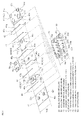
Fig. 5] Fig. 5 is a process drawing that shows a process for assembling the module assembly according to the first example of the present invention. - [
Fig. 6] Fig. 6(a) is a perspective view showing the appearance of a capacitor according to the first example of the present invention, andFig. 6(b) is a perspective view showing the appearance of a single-phase unit of the three-level inverter according to the first example of the present invention. - [
Fig. 7] Fig. 7 is a side view showing a configuration of the single-phase unit of the three-level inverter according to the first example of the present invention. - [
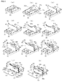
Fig. 8] Fig. 8 is a diagram showing flows of currents to explain the operations of the present invention. - [
Fig. 9] Fig. 9 is a perspective view showing the appearance of an assembly of two pairs of parallel modules according to a second example of the present invention. - [
Fig. 10] Fig. 10 is a perspective view showing the appearance of an assembly of three pairs of parallel modules according to a third example of the present invention. - [
Fig. 11] Fig. 11 is a circuit configuration diagram showing a configuration of a single phase of a typical three-level inverter. - [
Fig. 12] Fig. 12(a) is a plan view of a wiring structure of a conventional three-level inverter, andFig. 12(b) is a side view of the same. - Embodiments of the present invention are described based on the examples shown in the diagrams.
-
Fig. 1 is a circuit configuration diagram showing a single phase of a three-level inverter according to a first example of the present invention. - As shown in
Fig. 1 , afirst module 20 houses a circuit that configures a vertical arm of a three-level inverter, in which semiconductor switches 4 and 5 configured with MOSFETs are connected in series. A bidirectional switch functioning as an intermediate arm of the three-level inverter is configured withdiodes IGBTs second module 30. The semiconductor switches applied to the vertical arm and the intermediate arm are not limited to the example shown inFig. 1 , and therefore various semiconductor switches such as high-speed switching elements made from wide band-gap semiconductor materials such as SiC (silicon carbide) can be used in accordance with the specifications of the devices used. Wide band-gap semiconductor materials have recently been put into practical use. - A high-potential connecting terminal 20P connected to a high-potential terminal P of a DC power source, a low-potential connecting terminal 20N connected to a low-potential terminal N, an
output terminal 20U for extracting an AC output, and gate connecting terminals 20G4, 20G5 and auxiliary source terminals 20S4, 20S5 of the semiconductor switches 4, 5, are pulled out from themodule 20 configuring the vertical arm. - An intermediate-potential connecting terminal 30M connected to an intermediate-potential terminal M of the DC power source, a connecting
terminal 30U connected to theoutput terminal 20U of the vertical arm, and gate connecting terminals 30G12, 30G13 and auxiliary emitter terminals 30E12, 30E13 of the semiconductor switches 12, 13, are pulled out of themodule 30 configuring the intermediate arm. - In the
DC power source 1, aDC capacitor 2 is connected between the high-potential terminal P and the intermediate-potential terminal M of theDC power source 1, and aDC capacitor 3 is connected between the low-potential terminal N and the intermediate-potential terminal M of the same. The high-potential terminal P connected to thecapacitor 2 and the high-potential connecting terminal 20P of thevertical arm module 20 are connected to each other by a high-potential connection conductor 40P. The low-potential terminal N connected to thecapacitor 3 and the low-potential connecting terminal 20N of thevertical arm module 20 are connected to each other by a low-potential connection conductor 40N. The intermediate-potential connecting terminal 30M of theintermediate arm module 30 and the intermediate-potential terminal M are connected to each other by an intermediate-potential connection conductor 40M. Theoutput terminal 20U of thevertical arm module 20 and the output terminal connecting terminal 30U of theintermediate arm 30 are connected to each other by anoutput connection conductor 40U. Theseconnection conductors -
Fig. 2 shows the appearances of themodule 20 and themodule 30 that respectively configure the vertical arm and the intermediate arm shown inFig. 1 . Each of these modules is packaged air-tightly with an insulating resin block that houses the semiconductor switching elements. A plurality of connecting terminals are arranged on an upper surface of the block, and either end of the block is provided with mountingholes - Each of the connecting terminals provided in the
modules - The connecting
terminals vertical arm module 20 are the high-potential connecting terminal 20P, low-potential connecting terminal 20N, and output connecting terminal 20U of thevertical arm module 20 shown inFig. 1 . The connecting terminals 20G4 and 20G5 of themodule 20 are the gate terminals of the semiconductor switches 4 and 5 of thevertical arm 20 shown inFig. 1 , and the terminals 20S4 and 20S5 are the auxiliary source terminals. - The connecting
terminals intermediate arm module 30 are the intermediate-potential connecting terminal 30M and theoutput terminal 30U of theintermediate arm module 30 shown inFig. 1 . The connecting terminals 30G12 and 30G13 of theintermediate module 30 are the gate terminals of the semiconductor switches 12 and 13 of theintermediate arm 30 shown inFig. 1 , and the terminals 30E12 and 30E13 are the auxiliary emitter terminals. A terminal 30B of theintermediate arm module 30 is a vacant terminal, which is not for electrical connection but is provided for the purpose of making the terminal arrangement in theintermediate arm module 30 identical with the terminal arrangement in thevertical arm module 20. - An assembly of the three-level inverter according to the present invention is described next with reference to
Fig. 3 andFig. 4 . -
Fig. 3 is a configuration diagram of an assembly of a single-phase unit of the three-level inverter in which a connectingterminal board assembly 40 of the present invention is disposed on top of the two joinedmodules Fig. 2 . - The
modules substrate 70 configured with a radiator, and secured to the coolingsubstrate 70 by mountingscrews 40c. The connectingterminal board assembly 40 is fixedly disposed vertically across these twomodules - This connecting
terminal board assembly 40 is configured by stacking a plurality of upright terminal boards and insulating plates.Fig. 4 shows an exploded view of the connectingterminal board assembly 40 as the detail thereof cannot be seen clearly inFig. 3 . The connectingterminal board assembly 40 is therefore described hereinafter with reference toFig. 4 . - An
output terminal board 41 is a connecting terminal board configuring theconnection conductor 40U (Fig. 1 ) that connects theoutput terminals output terminal board 40U has, on its left end side inFig. 4 , a connectingend 41a, the entire width of which is bent at a right angle. This connectingend 41a is provided withfitting holes 41e into which the pin-shaped connectingterminals terminal board 41 onto the coolingsubstrate 70 are joined respectively tospacers 41d made of an insulating material at the right end side of theterminal board 41. Theterminal board 41 also hasscrew insertion holes 41f through which mounting screws are inserted, and theseinsertion holes 41f are positioned to face the mountingholes terminal board 41 is joined to themodules - Connecting
terminal boards potential connection conductor 40N and the high-potential conductor 40P shown inFig. 1 , and are each made from a flat conductive material. The connectingterminal boards module 20 side) inFig. 4 ,terminal connectors terminals module 20, and bent at right angles. In addition, external connecting ends 44b and 48b for external connection that are configured with screw terminals are bent at right angles and provided at the upper ends of the connectingterminal boards module 30 side), so as to be diagonal to theterminal connectors terminal connectors fitting holes terminals module 20 are inserted and fitted. - A connecting
terminal board 46 is a terminal board configuring the intermediate-potential connection conductor 40M shown inFig. 1 , and is formed from a flat conductive material. The connectingterminal board 46 has, on its lower end at the tip side (themodule 30 side), aterminal connector 46a that is bent at a right angle and connected to the connecting terminal 30M of themodule 30. An external connectingend 46b for external connection that is configured with a screw terminal is bent at a right angle and provided at the upper end of the connectingterminal board 46, at the far side (themodule 20 side), so as to be diagonal to theterminal connector 46a. This connectingterminal board 46 is accompanied by an auxiliaryterminal board 46s that is joined to the external connectingend 46b to cause it to protrude to the right and left. - The insulating
plates output terminal board 41 and the low-potential connectingterminal board 44. The lower end of the outermost insulatingplate 42 is bent outward in order to expand the insulation creepage distance, and the upper end of the same has a depressed portion 42g that allows the passage of the external connectingend 44b of the connectingterminal board 44 and adepressed portion 42h that allows the passage of theexternal connector 46b and auxiliaryterminal board 46s of the connectingterminal board 46. - An insulating
plate 45 is inserted between the connectingterminal boards depressed portion 45g that allows the passage of the auxiliaryterminal board 46s of the connectingterminal board 46. - An insulating
plate 47 is inserted between the connectingterminal boards module 20 side), a depressed portion 47g that allows the passage of the auxiliaryterminal board 46s of the connectingterminal board 46. - An insulating
plate 49 is inserted between the connectingterminal board 48 and agate circuit board 50 disposed on the outside of the connectingterminal board 48. - The
gate circuit board 50 is configured with, although not shown, a printed circuit board having gate drive circuits of the semiconductor switches of the respective modules. Thegate circuit board 50 has gateterminal connection holes 50e that are connected to thegate connecting terminals modules gate circuit board 50 also hasscrew insertion holes 50f through which the mountingscrews 40c are inserted. Thescrew insertion holes 50f are positioned to face the mountingholes modules - Because all of these connecting terminal boards and insulating plates are disposed across the entire width Wm of the two
modules Fig. 4 , the width W40 is substantially equal to the entire width Wm of the modules. However, in view of the functions of the insulating plates, it is preferred that the width W40 be slightly greater than the entire width Wm so that the insulating plates protrude slightly from the edges of the modules. - A process for assembling the three-level inverter having the
vertical arm module 20, theintermediate arm module 30, the connectingterminal board assembly 40, and thegate circuit board 50 is described hereinafter with reference toFig. 5 . - First, as shown in
Fig. 5(a) , themodule 20 and themodule 30 that respectively house the vertical arm and the intermediate arm configuring the three-level inverter, are disposed close to and parallel to each other, with thegate terminals - Next, as shown in
Fig. 5(b) , the output connectingterminal board 41 is placed horizontally on the right rear ends of themodules output connecting terminals fitting holes 41e. The connectingterminals fitting holes 41e are welded, brazed, or crimped (crushed) to electrically and mechanically join the connectingterminals terminal board 41, thereby securing the connectingterminal board 41. - After securing the connecting
terminal board 41 onto themodules plates terminal board 41, as shown inFigs. 5(c) and 5(d) . - Next, the low-potential connecting
terminal board 44 is disposed vertically in front of the insulatingplate 43, as shown inFig. 5(e) . In so doing, the connecting terminal 20N of themodule 20 is inserted and fitted into afitting hole 44e of the connectingend 44a of theterminal board 44 to electrically and mechanically join the connectingterminal board 44 and the connecting terminal 20N to each other by appropriate means, thereby securing the connectingterminal board 44. - Subsequently, the insulating
plate 45 is disposed vertically in front of the connectingterminal board 44, as shown inFig. 5(f) . - Then, the intermediate-potential connecting
terminal board 46 is disposed vertically in front of the insulatingplate 45, as shown inFig. 5(g) . Although not shown, the intermediate-potential connecting terminal 30M of themodule 30 is inserted and fitted intofitting holes 46e of the connectingend 46a of the connectingterminal board 46. The connectingterminal board 46 and the connecting terminal 30M are thereby joined to each other electrically and mechanically by appropriate means, thereby securing the connectingterminal board 46. Thescrew connecting end 46b at the upper end of the connectingterminal board 46 protrudes to the right through the depressed portions of the insulating plates. - Next, the insulating
plate 47 is disposed vertically in front of the connectingterminal board 46, as shown inFig. 5(h) . Subsequently, the high-potential connectingterminal board 48 is disposed vertically as shown inFig. 5(i) . The high-potential connecting terminal 20P of themodule 20 is inserted and fitted into thefitting holes 48e of the connectingend 48a located at the lower end of the connectingterminal board 48, to electrically and mechanically join the connectingterminal board 48 and the connecting terminal to each other, thereby securing the connectingterminal board 48. - Next, the insulating
plate 49 and thegate circuit board 50 are disposed vertically and horizontally, respectively, in front of the connectingterminal board 48, as shown inFig. 5(j) . The gate connecting terminals 20G4, 20G5 and auxiliary source terminals 20S4, 20S5 of themodule 20 and the gate connecting terminals 30G12, 30G13 and auxiliary emitter terminals 30E12, 30E13 of themodule 30 are inserted and fitted into thefitting hole 50e of thegate circuit board 50. Accordingly, thegate circuit board 50 is electrically and mechanically joined and secured to the gate terminals, the auxiliary source terminals, and the auxiliary emitter terminals. - Furthermore, the auxiliary
terminal board 46s is placed on the external connectingend 46b of the intermediate-potential connectingterminal board 46 to electrically and mechanically join them together in such a manner that the secrew connecting end projects to the right and left. - As a result, the module assembly in which the modules and the group of connecting terminals are joined is completed. Thereafter, DC capacitors for dividing a DC voltage to form a three-level (high potential, intermediate potential, low potential) DC voltage are connected between the connecting
end 44b and the auxiliaryterminal board 46s and between the connectingend 48b and the auxiliaryterminal board 46s in the module assembly, completing a single-phase unit of the three-level inverter. -
Fig. 6 shows the appearance of this completed single-phase unit of the three-level inverter, andFig. 7 is a side view showing the same.Fig. 6(a) shows aDC capacitor 60. TheDC capacitor 60 is provided with two connectingterminals end 44b and the auxiliaryterminal board 46, and the connectingend 44b and the auxiliaryterminal board 46. -
Fig. 6(b) andFig. 7 each show a configuration of the single-phase unit of the three-level inverter in which two DC capacitors 60-1 and 60-2 are joined to the module assembly. InFig. 6(b) , the capacitors 60-1 and 60-2 are shown transparently in order to clearly illustrate the connection states of the external connecting ends (44b, 46s, 48b) of the module assembly and terminals (61-1, 62-1, 61-2, 62-2) of the capacitors. - The capacitors 60-1 and 60-2 are each joined between the external connecting
end 48b of the high-potential connectingterminal board 48 of the module assembly and the auxiliaryterminal board 46s joined to the external connectingend 46b of the intermediate-potential connectingterminal board 46 and between the external connectingend 44b of the low-potential connectingterminal board 44 and the auxiliaryterminal board 46s joined to the external connectingend 46b of the intermediate-potential connectingterminal board 46. Thus, the single-phase unit of the three-level inverter with the circuit configuration shown inFig. 1 is configured. - In this configuration, the high-potential connecting
terminal board 48, intermediate-potential connectingterminal board 46, and low-potential connectingterminal board 44 that configure the DC circulating current paths are stacked close to and parallel to each other. Due to such a configuration, the magnetic fluxes of the currents flowing oppositely in these conductors offset each other, resulting in a reduction in wiring inductances of the DC circulating current paths of the single-phase unit of the three-level inverter. - In addition, according to the present invention, a wiring inductance of each connecting terminal board can be further reduced because the terminal connectors (44a, 46a, 48a) that connect the connecting terminal boards (44, 46, 48) to the connecting terminals of the modules, and the external connecting ends (44b, 46b, 48b) are positioned diagonally to each other on the upper and lower sides of the terminal boards, respectively.
- This point is now described with reference to
Fig. 8 . -
Fig. 8(a) is a diagram showing a flow of a current in each of the connecting terminal boards according to the present invention, which are provided with the connecting ends positioned diagonally to each other on the upper and lower sides of the connecting terminal boards, respectively. In comparison with the present invention,Fig. 8(b) is a diagram showing a flow of a current in each of the connecting terminal boards that are provided with the connecting ends positioned face-to-face at the upper and lower sides of the connecting terminal boards. - According to the present invention, the
terminal connector 48a, which is provided at the lower end of the high-potential connectingterminal board 48 and connected to the connecting terminal of the module, is provided on the lefthand side so as to be positioned immediately above themodule 20, while the external connectingend 48b on the upper end is provided on the right-hand side so as to be positioned immediately above themodule 30, as shown inFig. 8(a) . Therefore, theterminal connector 48a and external connectingend 48b of the connectingterminal board 48 are positioned diagonally to each other on the upper and lower sides of the connectingterminal board 48, respectively. Due to such a configuration, a current flows obliquely from the external connectingend 48b to theterminal connector 48a in the connectingterminal board 48, as shown by the solid arrow A. - On the connecting
terminal board 46, which is the intermediate-potential connection conductor disposed to face the connectingterminal board 48, theterminal connector 46a on the lower end is provided on the right-hand side so as to be positioned immediately above themodule 30, while the external connectingend 46b on the upper end is provided at the left end so as to be positioned immediately above themodule 20. Due to such a configuration, theterminal connector 46a and the external connectingend 46b, too, are positioned diagonally to each other on the upper and lower sides of the connectingterminal board 46, respectively. As a result, in the connectingterminal board 46, a current flows from theterminal connector 46a to the external connectingend 46b in the inclination direction opposite to the arrow A, as shown by the dotted arrow B. - Because the current shown by the arrow A and the current shown by the arrow B in the connecting
terminal boards - However, in a case where the
terminal connectors terminal boards - According to the present invention, such a difference in how the currents flow can be taken advantage of to reduce the wiring inductances of the DC circulating current paths.
-
Fig. 9 shows a second example of the present invention. In this example, themodule 20 housing the vertical arm and themodule 30 housing the intermediate arm are connected in two pairs and in parallel.Fig. 9 shows a simplified configuration of a connecting terminal board assembly without the insulating plates of the foregoing connecting terminal board assembly. - As shown in
Fig. 9 , two modules 20-1, 20-2 each housing a vertical arm and two modules 30-1, 30-2 each housing an intermediate arm are arranged alternately and in parallel. - These two pairs of modules that are disposed in parallel are provided with the connecting
terminal boards gate circuit board 50A, which are disposed across these two pairs of modules 20-1, 20-2 and 30-1, 30-2. - The high-potential connecting
terminal board 48A is provided with two terminal connectors (48a-1, 48a-2) connected to the connecting terminals of the modules 20-1 and 20-2 each housing a vertical arm, and two external connecting ends (48b-1, 48b-2) that are connected to the capacitors and the like. - The low-potential connecting
terminal board 44A is provided with two terminal connectors (not shown) that are connected to the connecting terminals of the modules 20-1 and 20-2 each housing a vertical arm, and two external connecting ends (44b-1, 44b-2) that are connected to the capacitors and the like. - The intermediate-potential connecting
terminal board 46A is provided with two terminal connectors (46a-1, 46a-2) that are connected to the connecting terminals of the modules 30-1 and 30-2 each housing an intermediate arm, and two external connecting ends (46b-1, 46b-2) that are connected to the capacitors and the like. - The capacitors are not shown in the diagram but are connected between the external connecting ends 48b-1 and 46b-1 at the upper portion of the connecting terminal boards, between the external connecting ends 44b-1 and 46b-1, between the external connecting ends 48b-2 and 46b-2, and between the external connecting ends 44b-2 and 46b-2, and disposed in the upper portions of the modules.
- The terminal connectors and the external connecting ends of the respective connecting terminal boards are located diagonally to each other in the respective pairs of modules. For instance, in the connecting
terminal board 48A, theterminal connector 48a-1 is positioned immediately above the module 20-1, and the external connectingend 48b-1 is positioned immediately above the module 30-1 paired with the module 20-1. Anotherterminal connector 48a-2 is positioned immediately above the module 20-2, and the external connectingend 48b-2 is positioned immediately above the module 30-2 paired with the module 20-2. - Therefore, in Example 2 as well, the magnetic fluxes of the currents flowing oppositely between these connecting terminal boards offset each other, resulting in a reduction in wiring inductances of the connecting terminal boards. Positioning the terminal connectors and external connecting ends of the connecting terminal boards diagonally to each other in the terminal boards can further reduce the wiring inductances of the connecting terminal boards as with Example 1.
-
Fig. 10 shows a third example of the present invention. In this example, the module housing the vertical arm and the module hosing the intermediate arm are connected in three pairs in parallel.Fig. 10 shows a simplified configuration of a connecting terminal board assembly without the insulating plates of the foregoing connecting terminal board assembly, as with Example 2. - As shown in
Fig. 10 , three modules 20-1, 20-2, 20-3 each housing a vertical arm and three modules 30-1, 30-2, 30-3 each housing an intermediate arm are arranged alternately and in parallel. - These three pairs of modules that are disposed in parallel are provided with the connecting
terminal boards gate circuit board 50B, which are disposed across the four modules 20-1, 20-2, 20-3, 30-1, 30-2, and 30-3. - The high-potential connecting
terminal board 48B is provided with three terminal connectors (48a-1, 48a-2, 48a-3) that are connected to the connecting terminals of the modules 20-1, 20-2 and 20-3 each housing a vertical arm, and three external connecting ends (48b-1, 48b-2, 48b-3) that are connected to the capacitors and the like. - The low-potential connecting
terminal board 44B is provided with three terminal connectors (not shown) that are connected to the connecting terminals of the modules 20-1, 20-2 and 20-3 each housing a vertical arm, and three external connecting ends (44b-1, 44b-2, 44b-3) that are connected to the capacitors and the like. - The intermediate-potential connecting
terminal board 46B is provided with three terminal connectors (46a-1, 46a-2, 46a-3) that are connected to the connecting terminals of the modules 30-1, 30-2 and 30-3 each having an intermediate arm, and three external connecting ends (46b-1, 46b-2, 46b-3) that are connected to the capacitors and the like. - The capacitors are not shown in the diagram but are connected between the external connecting ends 48b-1 and 46b-1 at the upper portions of the connecting terminal boards, between the external connecting ends 44b-1 and 46b-1, between the external connecting ends 48b-2 and 46b-2, between the external connecting ends 44b-2 and 46b-2, between the external connecting ends 48b-3 and 46b-3, and between the external connecting ends 44b-3 and 46b-3, and disposed in the upper portions of the modules.
- The terminal connectors and the external connecting ends of the respective connecting terminal boards are located diagonally to each other in the respective pairs of modules. For instance, in the connecting
terminal board 48B, theterminal connector 48a-1 is positioned immediately above the module 20-1, and the external connectingend 48b-1 is positioned immediately above the module 30-1 paired with the module 20-1. Anotherterminal connector 48a-2 is positioned immediately above the module 20-2, and the external connectingend 48b-2 is positioned immediately above the module 30-2 paired with the module 20-2. Theterminal connector 48a-1 is positioned immediately above the module 20-3, and the external connectingend 48b-1 is positioned immediately above the module 30-3 paired with the module 20-3. - Therefore, in Example 3 as well, the magnetic fluxes of the currents flowing oppositely between these connecting terminal boards offset each other, resulting in a reduction in wiring inductances of the connecting terminal boards. Positioning the terminal connectors and external connecting ends of the connecting terminal boards diagonally to each other in the terminal boards can further reduce the wiring inductances of the connecting terminal boards as with Example 1 and Example 2.
- Since the present invention can further reduce the wiring inductances of the DC circulating current paths in the three-level inverter as described above, the occurrence of a surge voltage can be prevented even when using a high-speed semiconductor switch in which semiconductor switches of a module housing a vertical arm are configured with wide band-gap (WBG) semiconductors such as SiC. Therefore, the performance and safety of the three-level inverter can further be improved.
-
- 20, 20-1, 20-2, 20-3 Module that houses vertical arm
- 30, 30-1, 30-2, 30-3 Module that houses intermediate arm
- 40 Connecting terminal board assembly
- 41 Connecting terminal board functioning as output connection conductor
- 41a Terminal connector
- 42, 43, 45, 47, 49 Insulating plate
- 44 Connecting terminal board functioning as low-potential connection conductor
- 44a, 44a-1, 44a-2, 44a-3 Terminal connector
- 44b, 44b-1, 44b-2, 44b-3 External connecting end
- 46 Connecting terminal board functioning as intermediate-potential connection conductor
- 46a, 46a-1, 46a-2, 46a-3 Terminal connector
- 44b, 46b-1, 46b-2, 46b-3 External connecting end
- 48 Connecting terminal board functioning as high-potential connection conductor
- 48a, 48a-1, 48a-2, 48a-3 Terminal connector
- 48b, 48b-1, 48b-2, 48b-3 External connecting end
- 50 Gate circuit board
Claims (5)
- A three-level power converter, comprising:a first module that houses a vertical arm configuring a three-level power conversion circuit;a second module that houses an intermediate arm configuring the three-level power conversion circuit and is disposed adjacent to the first module;a flat high-potential connecting terminal board which is pulled out vertically with a lower end thereof connected to a connecting terminal on an upper surface of the first module, the flat high-potential connecting terminal board having an upper end provided with an external connecting end;a flat low-potential connecting terminal board which is pulled out vertically with a lower end thereof connected to a connecting terminal on the upper surface of the first module, the flat low-potential connecting terminal board having an upper end provided with an external connecting end; anda flat intermediate-potential connecting terminal board which is pulled out vertically with a lower end thereof connected to a connecting terminal on an upper surface of the second module, the flat intermediate-potential connecting terminal board having an upper end provided with an external connecting end,wherein the high-potential connecting terminal board, the low-potential connecting terminal board, and the intermediate-potential connecting terminal board are stacked close to and parallel to one another, and a terminal of a DC capacitor is connected to each of the external connecting ends of these connecting terminal boards.
- The three-level power converter according to claim 1, wherein terminal connectors connected to the connecting terminals on the upper surfaces of the modules and the external connecting ends are positioned diagonally to each other on the connecting terminal boards.
- The three-level power converter according to claim 1 or 2, wherein the connecting terminals on the upper surfaces of the first module and the second module are pin-shaped terminals and arranged identically between the upper surfaces of the modules.
- The three-level power converter according to any one of claims 1 to 3, wherein
a plurality of modules pairs each configured with the first module and the second module are arranged in such a manner that the first modules and the second modules are disposed adjacent to each other alternately,
the high-potential connecting terminal board, the low-potential connecting terminal board, and the intermediate-potential connecting terminal board are formed across the entire modules of the plurality of module pairs, and
the plurality of module pairs are connected in parallel by the high-potential connecting terminal board, the low-potential connecting terminal board, and the intermediate-potential connecting terminal board. - The three-level power converter according to any one of claims 1 to 4, wherein a semiconductor switching element included in the first module is formed from a wide band-gap semiconductor.
Applications Claiming Priority (2)
| Application Number | Priority Date | Filing Date | Title |
|---|---|---|---|
| JP2014171698 | 2014-08-26 | ||
| PCT/JP2015/061544 WO2016031295A1 (en) | 2014-08-26 | 2015-04-15 | Three-level power conversion device |
Publications (3)
| Publication Number | Publication Date |
|---|---|
| EP3093974A1 true EP3093974A1 (en) | 2016-11-16 |
| EP3093974A4 EP3093974A4 (en) | 2017-10-18 |
| EP3093974B1 EP3093974B1 (en) | 2019-02-20 |
Family
ID=55399201
Family Applications (1)
| Application Number | Title | Priority Date | Filing Date |
|---|---|---|---|
| EP15836851.4A Not-in-force EP3093974B1 (en) | 2014-08-26 | 2015-04-15 | Three-level power conversion device |
Country Status (4)
| Country | Link |
|---|---|
| US (1) | US10153708B2 (en) |
| EP (1) | EP3093974B1 (en) |
| JP (1) | JP6160780B2 (en) |
| WO (1) | WO2016031295A1 (en) |
Cited By (2)
| Publication number | Priority date | Publication date | Assignee | Title |
|---|---|---|---|---|
| CN110574275A (en) * | 2017-04-27 | 2019-12-13 | 三菱电机株式会社 | power conversion unit |
| WO2021185431A1 (en) * | 2020-03-17 | 2021-09-23 | Huawei Technologies Co., Ltd. | Ac/dc converter stage for a converter system with an input series structure with improved common mode performance |
Families Citing this family (18)
| Publication number | Priority date | Publication date | Assignee | Title |
|---|---|---|---|---|
| JP6288301B2 (en) | 2014-11-28 | 2018-03-14 | 日産自動車株式会社 | Half-bridge power semiconductor module and manufacturing method thereof |
| CN105827129B (en) * | 2015-01-04 | 2020-06-02 | 华为技术有限公司 | Circuit and power converter with multi-level topology |
| JP6575072B2 (en) * | 2015-02-03 | 2019-09-18 | 富士電機株式会社 | Phase unit and three-level power converter using the same |
| WO2016129097A1 (en) * | 2015-02-13 | 2016-08-18 | 株式会社日産アーク | Half-bridge power semiconductor module, and method for manufacturing same |
| JP6429721B2 (en) * | 2015-05-07 | 2018-11-28 | 株式会社日立製作所 | Power converter and railway vehicle |
| ES2856875T3 (en) * | 2016-04-08 | 2021-09-28 | Toshiba Mitsubishi Electric Industrial Systems Corp | Multi-level power converter |
| JP6378714B2 (en) * | 2016-04-20 | 2018-08-22 | 矢崎総業株式会社 | Electrical junction box |
| JP6922175B2 (en) * | 2016-09-01 | 2021-08-18 | 富士電機株式会社 | Power converter |
| JP2018107857A (en) * | 2016-12-22 | 2018-07-05 | 富士電機株式会社 | Power conversion apparatus |
| US11271043B2 (en) * | 2017-04-19 | 2022-03-08 | Mitsubishi Electric Corporation | Semiconductor module and power conversion apparatus |
| WO2019180972A1 (en) * | 2018-03-23 | 2019-09-26 | 三菱電機株式会社 | Motor drive device, electric fan, vacuum cleaner, and hand dryer |
| US11070140B2 (en) * | 2018-10-25 | 2021-07-20 | Eaton Intelligent Power Limited | Low inductance bus assembly and power converter apparatus including the same |
| JP7283243B2 (en) * | 2019-06-13 | 2023-05-30 | 富士電機株式会社 | power converter |
| JP7443687B2 (en) * | 2019-07-23 | 2024-03-06 | 富士電機株式会社 | power converter |
| JP7380092B2 (en) * | 2019-11-05 | 2023-11-15 | 富士電機株式会社 | power converter |
| US12212224B2 (en) * | 2020-12-25 | 2025-01-28 | Fuji Electric Co., Ltd. | Driving apparatus |
| JP7459379B2 (en) * | 2021-05-13 | 2024-04-01 | 三菱電機株式会社 | power converter |
| JP7749955B2 (en) * | 2021-07-09 | 2025-10-07 | 富士電機株式会社 | Semiconductor module and manufacturing method thereof |
Family Cites Families (37)
| Publication number | Priority date | Publication date | Assignee | Title |
|---|---|---|---|---|
| US5731970A (en) * | 1989-12-22 | 1998-03-24 | Hitachi, Ltd. | Power conversion device and semiconductor module suitable for use in the device |
| EP0838855B1 (en) * | 1991-09-20 | 2004-11-24 | Hitachi, Ltd. | Semiconductor module |
| JP2692449B2 (en) * | 1991-10-01 | 1997-12-17 | 三菱電機株式会社 | Power module |
| JPH1189247A (en) | 1997-09-02 | 1999-03-30 | Denso Corp | Power converter |
| JP3424532B2 (en) * | 1997-11-25 | 2003-07-07 | 株式会社日立製作所 | Power converter |
| DE19833491A1 (en) * | 1998-07-24 | 2000-02-03 | Siemens Ag | Low-induction busbar for a three-point phase module |
| EP1330866B1 (en) * | 2000-11-03 | 2015-12-30 | SMC Electrical Products, Inc. | Inverter for use in an AC drive |
| JP3637276B2 (en) * | 2000-11-09 | 2005-04-13 | 株式会社日立製作所 | 3-level power converter |
| JP2004236470A (en) * | 2003-01-31 | 2004-08-19 | Yaskawa Electric Corp | Power module and power module integrated motor |
| US7505294B2 (en) * | 2003-05-16 | 2009-03-17 | Continental Automotive Systems Us, Inc. | Tri-level inverter |
| MX2008012609A (en) * | 2006-03-30 | 2008-12-16 | Mitsubishi Electric Corp | ENERGY CONVERSION DEVICE AND ITS MANUFACTURING METHOD. |
| JP2008193779A (en) * | 2007-02-02 | 2008-08-21 | Fuji Electric Systems Co Ltd | Semiconductor module |
| JP5369922B2 (en) | 2009-06-15 | 2013-12-18 | 富士電機株式会社 | 3-level power converter |
| JP2011010404A (en) * | 2009-06-24 | 2011-01-13 | Hitachi Ltd | Power converter, and electric motor drive device and transportation system employing the same |
| EP2302772A1 (en) * | 2009-09-28 | 2011-03-30 | ABB Oy | Inverter |
| CN102640408B (en) * | 2009-11-17 | 2015-05-20 | 三菱电机株式会社 | 3-level power conversion device |
| WO2011083737A1 (en) * | 2010-01-05 | 2011-07-14 | 富士電機システムズ株式会社 | Unit for semiconductor device, and semiconductor device |
| JP5494147B2 (en) * | 2010-04-06 | 2014-05-14 | 富士電機株式会社 | Power semiconductor module and power converter using the same |
| JP5440335B2 (en) * | 2010-04-06 | 2014-03-12 | 富士電機株式会社 | Power semiconductor module and power converter using the same |
| JP2012005301A (en) * | 2010-06-18 | 2012-01-05 | Fuji Electric Co Ltd | Power semiconductor module |
| AU2010356426B2 (en) * | 2010-07-01 | 2013-11-28 | Mitsubishi Electric Corporation | Power semiconductor module, electricity transformer device, and railway car |
| JP5024439B2 (en) * | 2010-09-24 | 2012-09-12 | 富士電機株式会社 | Semiconductor device |
| JP5724314B2 (en) * | 2010-11-16 | 2015-05-27 | 富士電機株式会社 | Power semiconductor module |
| WO2012169521A1 (en) * | 2011-06-10 | 2012-12-13 | 富士電機株式会社 | Semiconductor module, upper and lower arm kit and three-level inverter |
| JP5807516B2 (en) * | 2011-11-09 | 2015-11-10 | 株式会社明電舎 | Power converter and method of arranging conductor in power converter |
| WO2013145619A1 (en) * | 2012-03-28 | 2013-10-03 | 富士電機株式会社 | Semiconductor device and method for manufacturing semiconductor device |
| CN104170085B (en) | 2012-03-28 | 2017-05-10 | 富士电机株式会社 | Semiconductor device |
| EP2884650B1 (en) * | 2012-08-10 | 2018-09-19 | Mitsubishi Electric Corporation | Power module comprising two elements, and three-level power conversion device using same |
| CN102882385B (en) * | 2012-10-22 | 2015-09-23 | 台达电子工业股份有限公司 | Laminated busbar structure for three-level power converter and power converter |
| JP6102297B2 (en) * | 2013-02-06 | 2017-03-29 | 富士電機株式会社 | Semiconductor device |
| WO2014122877A1 (en) * | 2013-02-06 | 2014-08-14 | 富士電機株式会社 | Semiconductor device |
| CN104038085B (en) * | 2013-03-08 | 2016-07-06 | 台达电子工业股份有限公司 | Three Level Converter |
| JP6086157B2 (en) * | 2013-10-02 | 2017-03-01 | 富士電機株式会社 | 3-level inverter |
| CN103986354B (en) * | 2014-05-23 | 2016-10-12 | 台达电子企业管理(上海)有限公司 | Three-level rectifier |
| CN105450042B (en) * | 2014-09-26 | 2018-04-17 | 台达电子工业股份有限公司 | Three-level power converter and its power unit |
| US10123443B2 (en) * | 2014-12-25 | 2018-11-06 | Fuji Electric Co., Ltd. | Semiconductor device |
| JP2016197932A (en) * | 2015-04-02 | 2016-11-24 | 富士電機株式会社 | Semiconductor device |
-
2015
- 2015-04-15 JP JP2016544982A patent/JP6160780B2/en not_active Expired - Fee Related
- 2015-04-15 EP EP15836851.4A patent/EP3093974B1/en not_active Not-in-force
- 2015-04-15 WO PCT/JP2015/061544 patent/WO2016031295A1/en not_active Ceased
-
2016
- 2016-08-08 US US15/230,968 patent/US10153708B2/en active Active
Cited By (4)
| Publication number | Priority date | Publication date | Assignee | Title |
|---|---|---|---|---|
| CN110574275A (en) * | 2017-04-27 | 2019-12-13 | 三菱电机株式会社 | power conversion unit |
| CN110574275B (en) * | 2017-04-27 | 2021-04-30 | 三菱电机株式会社 | Power conversion unit |
| WO2021185431A1 (en) * | 2020-03-17 | 2021-09-23 | Huawei Technologies Co., Ltd. | Ac/dc converter stage for a converter system with an input series structure with improved common mode performance |
| US12191779B2 (en) | 2020-03-17 | 2025-01-07 | Huawei Digital Power Technologies Co., Ltd. | AC/DC converter stage for converter system with input series structure with improved common mode performance |
Also Published As
| Publication number | Publication date |
|---|---|
| EP3093974A4 (en) | 2017-10-18 |
| US20160344301A1 (en) | 2016-11-24 |
| JPWO2016031295A1 (en) | 2017-04-27 |
| US10153708B2 (en) | 2018-12-11 |
| EP3093974B1 (en) | 2019-02-20 |
| WO2016031295A1 (en) | 2016-03-03 |
| JP6160780B2 (en) | 2017-07-12 |
Similar Documents
| Publication | Publication Date | Title |
|---|---|---|
| EP3093974B1 (en) | Three-level power conversion device | |
| US7881086B2 (en) | Power conversion device and fabricating method for the same | |
| JP5132175B2 (en) | Power converter | |
| US20110216561A1 (en) | Low-Inductance Power Semiconductor Assembly | |
| JP6835144B2 (en) | Semiconductor unit, semiconductor device and uninterruptible power supply | |
| CN105742278A (en) | Semiconductor device | |
| CN111480231B (en) | power conversion device | |
| CN103238269A (en) | Power conversion device | |
| GB2539761A (en) | Power converter and railway vehicle | |
| US8897014B2 (en) | Mechanical layout for half-bridge power module that is optimized for low inductance | |
| CN103378745A (en) | Power conversion device | |
| JP6597549B2 (en) | Semiconductor module | |
| CN113632364B (en) | power conversion unit | |
| US10554123B2 (en) | Power converter with a parallel flat plate conductor electrically connected with a capacitor and a power module | |
| JP6526361B2 (en) | Power converter | |
| CN105593989A (en) | Semiconductor stack for converter with snubber-capacitor | |
| JP6575072B2 (en) | Phase unit and three-level power converter using the same | |
| JP2004056984A (en) | Power converter | |
| CN104380587B (en) | Power conversion device | |
| US11145634B2 (en) | Power converter | |
| JP2017005808A (en) | Power converter | |
| AU2016217603B2 (en) | Circuit module and inverter device using same | |
| JP4842018B2 (en) | Power converter | |
| JP2009089491A (en) | Power converter | |
| US20210211061A1 (en) | Converter |
Legal Events
| Date | Code | Title | Description |
|---|---|---|---|
| PUAI | Public reference made under article 153(3) epc to a published international application that has entered the european phase |
Free format text: ORIGINAL CODE: 0009012 |
|
| 17P | Request for examination filed |
Effective date: 20160810 |
|
| AK | Designated contracting states |
Kind code of ref document: A1 Designated state(s): AL AT BE BG CH CY CZ DE DK EE ES FI FR GB GR HR HU IE IS IT LI LT LU LV MC MK MT NL NO PL PT RO RS SE SI SK SM TR |
|
| AX | Request for extension of the european patent |
Extension state: BA ME |
|
| A4 | Supplementary search report drawn up and despatched |
Effective date: 20170914 |
|
| RIC1 | Information provided on ipc code assigned before grant |
Ipc: H02M 7/48 20070101AFI20170908BHEP Ipc: H02M 7/483 20070101ALI20170908BHEP |
|
| DAV | Request for validation of the european patent (deleted) | ||
| DAX | Request for extension of the european patent (deleted) | ||
| GRAP | Despatch of communication of intention to grant a patent |
Free format text: ORIGINAL CODE: EPIDOSNIGR1 |
|
| STAA | Information on the status of an ep patent application or granted ep patent |
Free format text: STATUS: GRANT OF PATENT IS INTENDED |
|
| INTG | Intention to grant announced |
Effective date: 20180814 |
|
| GRAS | Grant fee paid |
Free format text: ORIGINAL CODE: EPIDOSNIGR3 |
|
| GRAA | (expected) grant |
Free format text: ORIGINAL CODE: 0009210 |
|
| STAA | Information on the status of an ep patent application or granted ep patent |
Free format text: STATUS: THE PATENT HAS BEEN GRANTED |
|
| RIN1 | Information on inventor provided before grant (corrected) |
Inventor name: MARUYAMA, KOJI Inventor name: TANAKA, TAKAAKI |
|
| AK | Designated contracting states |
Kind code of ref document: B1 Designated state(s): AL AT BE BG CH CY CZ DE DK EE ES FI FR GB GR HR HU IE IS IT LI LT LU LV MC MK MT NL NO PL PT RO RS SE SI SK SM TR |
|
| REG | Reference to a national code |
Ref country code: GB Ref legal event code: FG4D |
|
| REG | Reference to a national code |
Ref country code: CH Ref legal event code: EP |
|
| REG | Reference to a national code |
Ref country code: DE Ref legal event code: R096 Ref document number: 602015025107 Country of ref document: DE |
|
| REG | Reference to a national code |
Ref country code: AT Ref legal event code: REF Ref document number: 1099490 Country of ref document: AT Kind code of ref document: T Effective date: 20190315 |
|
| REG | Reference to a national code |
Ref country code: IE Ref legal event code: FG4D |
|
| REG | Reference to a national code |
Ref country code: LT Ref legal event code: MG4D |
|
| REG | Reference to a national code |
Ref country code: NL Ref legal event code: MP Effective date: 20190220 |
|
| PG25 | Lapsed in a contracting state [announced via postgrant information from national office to epo] |
Ref country code: FI Free format text: LAPSE BECAUSE OF FAILURE TO SUBMIT A TRANSLATION OF THE DESCRIPTION OR TO PAY THE FEE WITHIN THE PRESCRIBED TIME-LIMIT Effective date: 20190220 Ref country code: NO Free format text: LAPSE BECAUSE OF FAILURE TO SUBMIT A TRANSLATION OF THE DESCRIPTION OR TO PAY THE FEE WITHIN THE PRESCRIBED TIME-LIMIT Effective date: 20190520 Ref country code: PT Free format text: LAPSE BECAUSE OF FAILURE TO SUBMIT A TRANSLATION OF THE DESCRIPTION OR TO PAY THE FEE WITHIN THE PRESCRIBED TIME-LIMIT Effective date: 20190620 Ref country code: SE Free format text: LAPSE BECAUSE OF FAILURE TO SUBMIT A TRANSLATION OF THE DESCRIPTION OR TO PAY THE FEE WITHIN THE PRESCRIBED TIME-LIMIT Effective date: 20190220 Ref country code: LT Free format text: LAPSE BECAUSE OF FAILURE TO SUBMIT A TRANSLATION OF THE DESCRIPTION OR TO PAY THE FEE WITHIN THE PRESCRIBED TIME-LIMIT Effective date: 20190220 |
|
| PG25 | Lapsed in a contracting state [announced via postgrant information from national office to epo] |
Ref country code: NL Free format text: LAPSE BECAUSE OF FAILURE TO SUBMIT A TRANSLATION OF THE DESCRIPTION OR TO PAY THE FEE WITHIN THE PRESCRIBED TIME-LIMIT Effective date: 20190220 Ref country code: LV Free format text: LAPSE BECAUSE OF FAILURE TO SUBMIT A TRANSLATION OF THE DESCRIPTION OR TO PAY THE FEE WITHIN THE PRESCRIBED TIME-LIMIT Effective date: 20190220 Ref country code: HR Free format text: LAPSE BECAUSE OF FAILURE TO SUBMIT A TRANSLATION OF THE DESCRIPTION OR TO PAY THE FEE WITHIN THE PRESCRIBED TIME-LIMIT Effective date: 20190220 Ref country code: IS Free format text: LAPSE BECAUSE OF FAILURE TO SUBMIT A TRANSLATION OF THE DESCRIPTION OR TO PAY THE FEE WITHIN THE PRESCRIBED TIME-LIMIT Effective date: 20190620 Ref country code: GR Free format text: LAPSE BECAUSE OF FAILURE TO SUBMIT A TRANSLATION OF THE DESCRIPTION OR TO PAY THE FEE WITHIN THE PRESCRIBED TIME-LIMIT Effective date: 20190521 Ref country code: BG Free format text: LAPSE BECAUSE OF FAILURE TO SUBMIT A TRANSLATION OF THE DESCRIPTION OR TO PAY THE FEE WITHIN THE PRESCRIBED TIME-LIMIT Effective date: 20190520 Ref country code: RS Free format text: LAPSE BECAUSE OF FAILURE TO SUBMIT A TRANSLATION OF THE DESCRIPTION OR TO PAY THE FEE WITHIN THE PRESCRIBED TIME-LIMIT Effective date: 20190220 |
|
| REG | Reference to a national code |
Ref country code: AT Ref legal event code: MK05 Ref document number: 1099490 Country of ref document: AT Kind code of ref document: T Effective date: 20190220 |
|
| PG25 | Lapsed in a contracting state [announced via postgrant information from national office to epo] |
Ref country code: DK Free format text: LAPSE BECAUSE OF FAILURE TO SUBMIT A TRANSLATION OF THE DESCRIPTION OR TO PAY THE FEE WITHIN THE PRESCRIBED TIME-LIMIT Effective date: 20190220 Ref country code: ES Free format text: LAPSE BECAUSE OF FAILURE TO SUBMIT A TRANSLATION OF THE DESCRIPTION OR TO PAY THE FEE WITHIN THE PRESCRIBED TIME-LIMIT Effective date: 20190220 Ref country code: EE Free format text: LAPSE BECAUSE OF FAILURE TO SUBMIT A TRANSLATION OF THE DESCRIPTION OR TO PAY THE FEE WITHIN THE PRESCRIBED TIME-LIMIT Effective date: 20190220 Ref country code: CZ Free format text: LAPSE BECAUSE OF FAILURE TO SUBMIT A TRANSLATION OF THE DESCRIPTION OR TO PAY THE FEE WITHIN THE PRESCRIBED TIME-LIMIT Effective date: 20190220 Ref country code: RO Free format text: LAPSE BECAUSE OF FAILURE TO SUBMIT A TRANSLATION OF THE DESCRIPTION OR TO PAY THE FEE WITHIN THE PRESCRIBED TIME-LIMIT Effective date: 20190220 Ref country code: IT Free format text: LAPSE BECAUSE OF FAILURE TO SUBMIT A TRANSLATION OF THE DESCRIPTION OR TO PAY THE FEE WITHIN THE PRESCRIBED TIME-LIMIT Effective date: 20190220 Ref country code: AL Free format text: LAPSE BECAUSE OF FAILURE TO SUBMIT A TRANSLATION OF THE DESCRIPTION OR TO PAY THE FEE WITHIN THE PRESCRIBED TIME-LIMIT Effective date: 20190220 Ref country code: SK Free format text: LAPSE BECAUSE OF FAILURE TO SUBMIT A TRANSLATION OF THE DESCRIPTION OR TO PAY THE FEE WITHIN THE PRESCRIBED TIME-LIMIT Effective date: 20190220 |
|
| REG | Reference to a national code |
Ref country code: DE Ref legal event code: R097 Ref document number: 602015025107 Country of ref document: DE |
|
| PG25 | Lapsed in a contracting state [announced via postgrant information from national office to epo] |
Ref country code: SM Free format text: LAPSE BECAUSE OF FAILURE TO SUBMIT A TRANSLATION OF THE DESCRIPTION OR TO PAY THE FEE WITHIN THE PRESCRIBED TIME-LIMIT Effective date: 20190220 Ref country code: PL Free format text: LAPSE BECAUSE OF FAILURE TO SUBMIT A TRANSLATION OF THE DESCRIPTION OR TO PAY THE FEE WITHIN THE PRESCRIBED TIME-LIMIT Effective date: 20190220 |
|
| REG | Reference to a national code |
Ref country code: CH Ref legal event code: PL |
|
| REG | Reference to a national code |
Ref country code: BE Ref legal event code: MM Effective date: 20190430 |
|
| PLBE | No opposition filed within time limit |
Free format text: ORIGINAL CODE: 0009261 |
|
| STAA | Information on the status of an ep patent application or granted ep patent |
Free format text: STATUS: NO OPPOSITION FILED WITHIN TIME LIMIT |
|
| PG25 | Lapsed in a contracting state [announced via postgrant information from national office to epo] |
Ref country code: MC Free format text: LAPSE BECAUSE OF FAILURE TO SUBMIT A TRANSLATION OF THE DESCRIPTION OR TO PAY THE FEE WITHIN THE PRESCRIBED TIME-LIMIT Effective date: 20190220 Ref country code: AT Free format text: LAPSE BECAUSE OF FAILURE TO SUBMIT A TRANSLATION OF THE DESCRIPTION OR TO PAY THE FEE WITHIN THE PRESCRIBED TIME-LIMIT Effective date: 20190220 Ref country code: LU Free format text: LAPSE BECAUSE OF NON-PAYMENT OF DUE FEES Effective date: 20190415 |
|
| 26N | No opposition filed |
Effective date: 20191121 |
|
| GBPC | Gb: european patent ceased through non-payment of renewal fee |
Effective date: 20190520 |
|
| PG25 | Lapsed in a contracting state [announced via postgrant information from national office to epo] |
Ref country code: LI Free format text: LAPSE BECAUSE OF NON-PAYMENT OF DUE FEES Effective date: 20190430 Ref country code: CH Free format text: LAPSE BECAUSE OF NON-PAYMENT OF DUE FEES Effective date: 20190430 |
|
| PG25 | Lapsed in a contracting state [announced via postgrant information from national office to epo] |
Ref country code: BE Free format text: LAPSE BECAUSE OF NON-PAYMENT OF DUE FEES Effective date: 20190430 Ref country code: FR Free format text: LAPSE BECAUSE OF NON-PAYMENT OF DUE FEES Effective date: 20190420 Ref country code: SI Free format text: LAPSE BECAUSE OF FAILURE TO SUBMIT A TRANSLATION OF THE DESCRIPTION OR TO PAY THE FEE WITHIN THE PRESCRIBED TIME-LIMIT Effective date: 20190220 |
|
| PG25 | Lapsed in a contracting state [announced via postgrant information from national office to epo] |
Ref country code: TR Free format text: LAPSE BECAUSE OF FAILURE TO SUBMIT A TRANSLATION OF THE DESCRIPTION OR TO PAY THE FEE WITHIN THE PRESCRIBED TIME-LIMIT Effective date: 20190220 |
|
| PG25 | Lapsed in a contracting state [announced via postgrant information from national office to epo] |
Ref country code: IE Free format text: LAPSE BECAUSE OF NON-PAYMENT OF DUE FEES Effective date: 20190415 Ref country code: GB Free format text: LAPSE BECAUSE OF NON-PAYMENT OF DUE FEES Effective date: 20190520 |
|
| PG25 | Lapsed in a contracting state [announced via postgrant information from national office to epo] |
Ref country code: CY Free format text: LAPSE BECAUSE OF FAILURE TO SUBMIT A TRANSLATION OF THE DESCRIPTION OR TO PAY THE FEE WITHIN THE PRESCRIBED TIME-LIMIT Effective date: 20190220 |
|
| PG25 | Lapsed in a contracting state [announced via postgrant information from national office to epo] |
Ref country code: HU Free format text: LAPSE BECAUSE OF FAILURE TO SUBMIT A TRANSLATION OF THE DESCRIPTION OR TO PAY THE FEE WITHIN THE PRESCRIBED TIME-LIMIT; INVALID AB INITIO Effective date: 20150415 Ref country code: MT Free format text: LAPSE BECAUSE OF FAILURE TO SUBMIT A TRANSLATION OF THE DESCRIPTION OR TO PAY THE FEE WITHIN THE PRESCRIBED TIME-LIMIT Effective date: 20190220 |
|
| PG25 | Lapsed in a contracting state [announced via postgrant information from national office to epo] |
Ref country code: MK Free format text: LAPSE BECAUSE OF FAILURE TO SUBMIT A TRANSLATION OF THE DESCRIPTION OR TO PAY THE FEE WITHIN THE PRESCRIBED TIME-LIMIT Effective date: 20190220 |
|
| PGFP | Annual fee paid to national office [announced via postgrant information from national office to epo] |
Ref country code: DE Payment date: 20230228 Year of fee payment: 9 |
|
| REG | Reference to a national code |
Ref country code: DE Ref legal event code: R119 Ref document number: 602015025107 Country of ref document: DE |
|
| PG25 | Lapsed in a contracting state [announced via postgrant information from national office to epo] |
Ref country code: DE Free format text: LAPSE BECAUSE OF NON-PAYMENT OF DUE FEES Effective date: 20241105 |
|
| PG25 | Lapsed in a contracting state [announced via postgrant information from national office to epo] |
Ref country code: DE Free format text: LAPSE BECAUSE OF NON-PAYMENT OF DUE FEES Effective date: 20241105 |