EP3091651A1 - Power supply device - Google Patents
Power supply device Download PDFInfo
- Publication number
- EP3091651A1 EP3091651A1 EP15864317.1A EP15864317A EP3091651A1 EP 3091651 A1 EP3091651 A1 EP 3091651A1 EP 15864317 A EP15864317 A EP 15864317A EP 3091651 A1 EP3091651 A1 EP 3091651A1
- Authority
- EP
- European Patent Office
- Prior art keywords
- voltage
- protection
- power supply
- unit
- protection voltage
- Prior art date
- Legal status (The legal status is an assumption and is not a legal conclusion. Google has not performed a legal analysis and makes no representation as to the accuracy of the status listed.)
- Granted
Links
Images


Classifications
-
- H—ELECTRICITY
- H02—GENERATION; CONVERSION OR DISTRIBUTION OF ELECTRIC POWER
- H02M—APPARATUS FOR CONVERSION BETWEEN AC AND AC, BETWEEN AC AND DC, OR BETWEEN DC AND DC, AND FOR USE WITH MAINS OR SIMILAR POWER SUPPLY SYSTEMS; CONVERSION OF DC OR AC INPUT POWER INTO SURGE OUTPUT POWER; CONTROL OR REGULATION THEREOF
- H02M1/00—Details of apparatus for conversion
- H02M1/42—Circuits or arrangements for compensating for or adjusting power factor in converters or inverters
- H02M1/4208—Arrangements for improving power factor of AC input
- H02M1/4225—Arrangements for improving power factor of AC input using a non-isolated boost converter
-
- H—ELECTRICITY
- H02—GENERATION; CONVERSION OR DISTRIBUTION OF ELECTRIC POWER
- H02H—EMERGENCY PROTECTIVE CIRCUIT ARRANGEMENTS
- H02H3/00—Emergency protective circuit arrangements for automatic disconnection directly responsive to an undesired change from normal electric working condition with or without subsequent reconnection ; integrated protection
- H02H3/24—Emergency protective circuit arrangements for automatic disconnection directly responsive to an undesired change from normal electric working condition with or without subsequent reconnection ; integrated protection responsive to undervoltage or no-voltage
-
- H—ELECTRICITY
- H02—GENERATION; CONVERSION OR DISTRIBUTION OF ELECTRIC POWER
- H02H—EMERGENCY PROTECTIVE CIRCUIT ARRANGEMENTS
- H02H7/00—Emergency protective circuit arrangements specially adapted for specific types of electric machines or apparatus or for sectionalised protection of cable or line systems, and effecting automatic switching in the event of an undesired change from normal working conditions
- H02H7/10—Emergency protective circuit arrangements specially adapted for specific types of electric machines or apparatus or for sectionalised protection of cable or line systems, and effecting automatic switching in the event of an undesired change from normal working conditions for converters; for rectifiers
- H02H7/12—Emergency protective circuit arrangements specially adapted for specific types of electric machines or apparatus or for sectionalised protection of cable or line systems, and effecting automatic switching in the event of an undesired change from normal working conditions for converters; for rectifiers for static converters or rectifiers
- H02H7/125—Emergency protective circuit arrangements specially adapted for specific types of electric machines or apparatus or for sectionalised protection of cable or line systems, and effecting automatic switching in the event of an undesired change from normal working conditions for converters; for rectifiers for static converters or rectifiers for rectifiers
-
- H—ELECTRICITY
- H02—GENERATION; CONVERSION OR DISTRIBUTION OF ELECTRIC POWER
- H02H—EMERGENCY PROTECTIVE CIRCUIT ARRANGEMENTS
- H02H9/00—Emergency protective circuit arrangements for limiting excess current or voltage without disconnection
- H02H9/001—Emergency protective circuit arrangements for limiting excess current or voltage without disconnection limiting speed of change of electric quantities, e.g. soft switching on or off
-
- H—ELECTRICITY
- H02—GENERATION; CONVERSION OR DISTRIBUTION OF ELECTRIC POWER
- H02M—APPARATUS FOR CONVERSION BETWEEN AC AND AC, BETWEEN AC AND DC, OR BETWEEN DC AND DC, AND FOR USE WITH MAINS OR SIMILAR POWER SUPPLY SYSTEMS; CONVERSION OF DC OR AC INPUT POWER INTO SURGE OUTPUT POWER; CONTROL OR REGULATION THEREOF
- H02M3/00—Conversion of DC power input into DC power output
- H02M3/02—Conversion of DC power input into DC power output without intermediate conversion into AC
- H02M3/04—Conversion of DC power input into DC power output without intermediate conversion into AC by static converters
- H02M3/10—Conversion of DC power input into DC power output without intermediate conversion into AC by static converters using discharge tubes with control electrode or semiconductor devices with control electrode
- H02M3/145—Conversion of DC power input into DC power output without intermediate conversion into AC by static converters using discharge tubes with control electrode or semiconductor devices with control electrode using devices of a triode or transistor type requiring continuous application of a control signal
- H02M3/155—Conversion of DC power input into DC power output without intermediate conversion into AC by static converters using discharge tubes with control electrode or semiconductor devices with control electrode using devices of a triode or transistor type requiring continuous application of a control signal using semiconductor devices only
-
- H—ELECTRICITY
- H02—GENERATION; CONVERSION OR DISTRIBUTION OF ELECTRIC POWER
- H02M—APPARATUS FOR CONVERSION BETWEEN AC AND AC, BETWEEN AC AND DC, OR BETWEEN DC AND DC, AND FOR USE WITH MAINS OR SIMILAR POWER SUPPLY SYSTEMS; CONVERSION OF DC OR AC INPUT POWER INTO SURGE OUTPUT POWER; CONTROL OR REGULATION THEREOF
- H02M7/00—Conversion of AC power input into DC power output; Conversion of DC power input into AC power output
- H02M7/02—Conversion of AC power input into DC power output without possibility of reversal
- H02M7/04—Conversion of AC power input into DC power output without possibility of reversal by static converters
- H02M7/06—Conversion of AC power input into DC power output without possibility of reversal by static converters using discharge tubes without control electrode or semiconductor devices without control electrode
-
- H—ELECTRICITY
- H02—GENERATION; CONVERSION OR DISTRIBUTION OF ELECTRIC POWER
- H02M—APPARATUS FOR CONVERSION BETWEEN AC AND AC, BETWEEN AC AND DC, OR BETWEEN DC AND DC, AND FOR USE WITH MAINS OR SIMILAR POWER SUPPLY SYSTEMS; CONVERSION OF DC OR AC INPUT POWER INTO SURGE OUTPUT POWER; CONTROL OR REGULATION THEREOF
- H02M7/00—Conversion of AC power input into DC power output; Conversion of DC power input into AC power output
- H02M7/02—Conversion of AC power input into DC power output without possibility of reversal
- H02M7/04—Conversion of AC power input into DC power output without possibility of reversal by static converters
- H02M7/12—Conversion of AC power input into DC power output without possibility of reversal by static converters using discharge tubes with control electrode or semiconductor devices with control electrode
- H02M7/21—Conversion of AC power input into DC power output without possibility of reversal by static converters using discharge tubes with control electrode or semiconductor devices with control electrode using devices of a triode or transistor type requiring continuous application of a control signal
- H02M7/217—Conversion of AC power input into DC power output without possibility of reversal by static converters using discharge tubes with control electrode or semiconductor devices with control electrode using devices of a triode or transistor type requiring continuous application of a control signal using semiconductor devices only
-
- H—ELECTRICITY
- H10—SEMICONDUCTOR DEVICES; ELECTRIC SOLID-STATE DEVICES NOT OTHERWISE PROVIDED FOR
- H10D—INORGANIC ELECTRIC SEMICONDUCTOR DEVICES
- H10D62/00—Semiconductor bodies, or regions thereof, of devices having potential barriers
- H10D62/80—Semiconductor bodies, or regions thereof, of devices having potential barriers characterised by the materials
- H10D62/83—Semiconductor bodies, or regions thereof, of devices having potential barriers characterised by the materials being Group IV materials, e.g. B-doped Si or undoped Ge
- H10D62/832—Semiconductor bodies, or regions thereof, of devices having potential barriers characterised by the materials being Group IV materials, e.g. B-doped Si or undoped Ge being Group IV materials comprising two or more elements, e.g. SiGe
- H10D62/8325—Silicon carbide
-
- H—ELECTRICITY
- H02—GENERATION; CONVERSION OR DISTRIBUTION OF ELECTRIC POWER
- H02M—APPARATUS FOR CONVERSION BETWEEN AC AND AC, BETWEEN AC AND DC, OR BETWEEN DC AND DC, AND FOR USE WITH MAINS OR SIMILAR POWER SUPPLY SYSTEMS; CONVERSION OF DC OR AC INPUT POWER INTO SURGE OUTPUT POWER; CONTROL OR REGULATION THEREOF
- H02M1/00—Details of apparatus for conversion
- H02M1/0003—Details of control, feedback or regulation circuits
- H02M1/0025—Arrangements for modifying reference values, feedback values or error values in the control loop of a converter
-
- H—ELECTRICITY
- H10—SEMICONDUCTOR DEVICES; ELECTRIC SOLID-STATE DEVICES NOT OTHERWISE PROVIDED FOR
- H10D—INORGANIC ELECTRIC SEMICONDUCTOR DEVICES
- H10D62/00—Semiconductor bodies, or regions thereof, of devices having potential barriers
- H10D62/80—Semiconductor bodies, or regions thereof, of devices having potential barriers characterised by the materials
- H10D62/83—Semiconductor bodies, or regions thereof, of devices having potential barriers characterised by the materials being Group IV materials, e.g. B-doped Si or undoped Ge
- H10D62/8303—Diamond
-
- H—ELECTRICITY
- H10—SEMICONDUCTOR DEVICES; ELECTRIC SOLID-STATE DEVICES NOT OTHERWISE PROVIDED FOR
- H10D—INORGANIC ELECTRIC SEMICONDUCTOR DEVICES
- H10D62/00—Semiconductor bodies, or regions thereof, of devices having potential barriers
- H10D62/80—Semiconductor bodies, or regions thereof, of devices having potential barriers characterised by the materials
- H10D62/85—Semiconductor bodies, or regions thereof, of devices having potential barriers characterised by the materials being Group III-V materials, e.g. GaAs
- H10D62/8503—Nitride Group III-V materials, e.g. AlN or GaN
-
- Y—GENERAL TAGGING OF NEW TECHNOLOGICAL DEVELOPMENTS; GENERAL TAGGING OF CROSS-SECTIONAL TECHNOLOGIES SPANNING OVER SEVERAL SECTIONS OF THE IPC; TECHNICAL SUBJECTS COVERED BY FORMER USPC CROSS-REFERENCE ART COLLECTIONS [XRACs] AND DIGESTS
- Y02—TECHNOLOGIES OR APPLICATIONS FOR MITIGATION OR ADAPTATION AGAINST CLIMATE CHANGE
- Y02B—CLIMATE CHANGE MITIGATION TECHNOLOGIES RELATED TO BUILDINGS, e.g. HOUSING, HOUSE APPLIANCES OR RELATED END-USER APPLICATIONS
- Y02B70/00—Technologies for an efficient end-user side electric power management and consumption
- Y02B70/10—Technologies improving the efficiency by using switched-mode power supplies [SMPS], i.e. efficient power electronics conversion e.g. power factor correction or reduction of losses in power supplies or efficient standby modes
Definitions
- the present invention relates to a power supply device that converts an AC voltage to a DC voltage.
- the power supply device When the power is turned on for a power supply device, there may be an inrush current that flows in the power supply device when a smoothing capacitor is charged.
- the power supply device adopts a configuration in which a resistor is connected in series with the smoothing capacitor, thereby suppressing the inrush current when the power is turned on.
- Patent Literature 1 such a power supply device is disclosed in which a relay is connected across an overcurrent protection circuit that includes an inrush-current suppressing resistor.
- the relay When the power is turned on, the relay is opened and the charging current of the smoothing capacitor is consumed as heat by the inrush current limit resistor, thereby suppressing the inrush current when the power is turned on.
- the power supply device disclosed in Patent Literature 1 closes the relay and isolates the inrush-current suppressing resistor, thereby causing the current to flow to the relay without bypassing the inrush-current suppressing resistor.
- Patent Literature 2 discloses a power supply device in which, when a momentary cutoff of the power supply occurs due to an instantaneous power failure, the voltage across the smoothing capacitor is compared with a set protection voltage, and the relay connected in parallel with the inrush-current limiting resistor is controlled on the basis of the comparison result, thereby suppressing the inrush current.
- the magnitude of the inrush current occurring at the time of recovery from an instantaneous power failure depends on the difference between the voltage across the smoothing capacitor immediately before the recovery from the instantaneous power failure and the AC voltage at the time of recovery from the instantaneous power failure. Therefore, to suppress the inrush current within a protection voltage set range, the power supply device in Patent Literature 2 needs to be configured from an expensive element that has high current durability and is capable of enduring the inrush current.
- the present invention has been achieved in view of the above problems, and an object of the present invention is to provide a power supply device that can suppress an inrush current generated at the time of recovery from a power failure, without using an element that has high current durability and is capable of enduring the inrush current and without being affected by an operating state of a booster circuit unit and fluctuations in an AC voltage.
- a power supply device includes: a resistor that limits an electric current supplied from an alternating-current power supply; a switching unit that is connected in parallel with the resistor; a rectifier circuit unit that is connected to a subsequent stage of the resistor and the switching unit and rectifies an alternating-current voltage of the alternating-current power supply; a booster circuit unit that boosts a direct-current voltage rectified by the rectifier circuit unit; a direct-current-voltage detection unit that detects a direct-current voltage output from the booster circuit unit; an alternating-current-voltage detection unit that detects an alternating-current voltage of the alternating-current power supply; a protection setting unit that calculates a first protection voltage on a basis of a boosting level by the booster circuit unit, calculates a second protection voltage on a basis of the alternating-current voltage detected by the alternating-current-voltage detection unit, compares the first protection voltage with the second protection voltage, and sets either one of the
- the present invention it is possible to suppress an inrush current generated at the time of recovery from a power failure without being affected by the operating state of a booster circuit unit and fluctuations in an AC voltage.
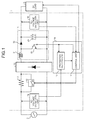
- FIG. 1 is a configuration diagram of a power supply device 1 according to an embodiment.
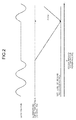
- FIG. 2 is a diagram illustrating a relation between a set level of a second protection voltage and a limit value with respect to an inrush current of a semiconductor element constituting a booster circuit unit.
- FIG. 3 is a diagram illustrating, in a case when a booster circuit unit has stopped, an operation of a power supply device from when an instantaneous power failure occurs to when an AC power supply is recovered.
- FIG. 4 is a diagram illustrating, in a case when a booster circuit unit is operating, an operation of a power supply device from when an instantaneous power failure occurs to when an AC power supply is recovered when a first protection voltage is set as a protection voltage.
- FIG. 1 is a configuration diagram of a power supply device 1 according to an embodiment.
- FIG. 2 is a diagram illustrating a relation between a set level of a second protection voltage and a limit value with respect to an inrush current of a semiconductor element constituting
- FIG. 5 is a diagram illustrating, in a case when a booster circuit unit is operating, an operation of a power supply device from when an instantaneous power failure occurs to when an AC power supply is recovered during the passage of a first transition period.
- FIG. 6 is a diagram illustrating, in a case when a booster circuit unit is operating, an operation of a power supply device from when an instantaneous power failure occurs to when an AC power supply is recovered when a second protection voltage is set as a protection voltage.
- FIG. 7 is a diagram illustrating an operation of a power supply device when setting a protection voltage in a case when a booster circuit unit is changed from an operating state to a shutdown state.
- FIG. 8 is a block diagram illustrating a configuration of an operation control unit 18 according to the embodiment.
- the power supply device 1 is connected to a DC load 3 and an AC power supply 2, which is an external power supply.
- the power supply device 1 converts an AC voltage supplied from the AC power supply 2 to a DC voltage and supplies the converted DC voltage to the DC load 3.
- the power supply device 1 includes a resistor 11 that limits an electric current; a switching unit 12 that switches between open and closed; a rectifier circuit unit 13 that rectifies an AC voltage; a booster circuit unit 14 that boosts a DC voltage; a DC-voltage detection unit 15 that detects a DC voltage; a protection setting unit 16 that sets a protection voltage; a control unit 17 that controls the switching unit 12 and the booster circuit unit 14; and an AC-voltage detection unit 19 that detects the AC voltage.
- the protection setting unit 16 and the control unit 17 constitute the operation control unit 18.
- the resistor 11 limits an inrush current supplied from the AC power supply 2 at the time of recovery from a power failure.
- the switching unit 12 is configured from a relay and is connected in parallel with the resistor 11.
- the switching unit 12 can be configured not from a relay, but from an IGBT (Insulated Gate Bipolar Transistor) or a MOSFET (Metal-Oxide-Semiconductor Field-Effect Transistor).
- IGBT Insulated Gate Bipolar Transistor
- MOSFET Metal-Oxide-Semiconductor Field-Effect Transistor
- the rectifier circuit unit 13 is connected to a subsequent stage of the resistor 11 and the switching unit 12 and rectifies the AC voltage.
- the booster circuit unit 14 is also referred to as a "boost chopper circuit unit” and boosts the DC voltage rectified by the rectifier circuit unit 13 up to a set voltage.
- the configuration of the booster circuit unit 14 is described here.
- the booster circuit unit 14 includes a boosting reactor 21, a switching element 22 that performs switching, a diode 23 that prevents backflow, and a smoothing capacitor 24 that smooths the voltage rectified by the rectifier circuit unit 13.
- An IGBT or a MOSFET is exemplified as the switching element 22.
- the reactor 21 and the diode 23 are connected in series between the high voltage side of the rectifier circuit unit 13 and the smoothing capacitor 24.
- the anode of the diode 23 is connected to the reactor 21 and the cathode of the diode 23 is connected to the DC load 3.
- the switching element 22 is connected between the reactor 21 and the diode 23 and on the wire that connects the high voltage side and the low voltage side.
- the booster circuit unit 14 When the switching element 22 is in an on-state, the booster circuit unit 14 accumulates energy in the reactor 21, and when the switching element 22 is in an off-state, the booster circuit unit 14 charges the smoothing capacitor 24 by using a back electromotive force generated in the reactor 21.
- the booster circuit unit 14 repeatedly switches the switching element 22 between an on-state and an off-state every set cycle to perform a boosting operation.
- the set cycle is a cycle with which a boosting operation can be performed.
- the switching element 22 and the diode 23, which are semiconductor elements constituting the booster circuit unit, can be wide bandgap semiconductors.
- the wide bandgap semiconductor can be SiC, GaN, or diamond.
- the booster circuit unit 14 is not limited to having the above configuration, and can have any configuration that can rectify the AC power supply and boost the voltage to an arbitrary DC voltage.
- the smoothing capacitor 24 repeats charging and discharging to smooth the voltage.
- the booster circuit unit 14 When boosting is not performed, the booster circuit unit 14 operates as a passive converter by setting the switching element 22 to always be in an off-state, and smooths the voltage rectified by the rectifier circuit unit 13 without boosting the voltage to supply the voltage to the DC load 3.
- the DC-voltage detection unit 15 detects the smoothing capacitor voltage that is a DC voltage output from the booster circuit unit 14. Specifically, the DC-voltage detection unit 15 detects the smoothing capacitor voltage that is the voltage across the smoothing capacitor 24. The smoothing capacitor voltage is equal to the DC bus voltage.
- the protection setting unit 16 always acquires a control signal that is output from the control unit 17 to the booster circuit unit 14, and ascertains a boosting level, which indicates an operating state of the booster circuit unit 14, and a shutdown state thereof on the basis of the control signal.
- the protection setting unit 16 calculates the first protection voltage on the basis of the boosting level by the booster circuit unit 14 and calculates the second protection voltage on the basis of the AC voltage detected by the AC-voltage detection unit 19 to compare the first protection voltage with the second protection voltage and set either one as a protection voltage.
- Such a configuration is also possible in which the first protection voltage is newly calculated on the basis of a boosting level L1 updated at an arbitrary timing by the control unit 17, and the new first protection voltage is compared with the second protection voltage to set either one as the protection voltage.
- the control unit 17 compares the smoothing capacitor voltage detected by the DC-voltage detection unit 15 with the protection voltage set by the protection setting unit 16. On the basis of the comparison result, the control unit 17 causes the booster circuit unit 14 to stop or perform boosting, causes the switching unit 12 to open or close the switch, and stops or starts the operation of the DC load 3. Specifically, when the smoothing capacitor voltage falls below the protection voltage, the control unit 17 causes the switching unit 12 to open the switch, causes the booster circuit unit 14 to stop boosting, and stops the operation of the DC load 3.
- FIG. 2 illustrates a waveform of an AC voltage supplied from the AC power supply 2.
- FIG. 2 illustrates a waveform of a smoothing capacitor voltage detected by the DC-voltage detection unit 15.
- the protection setting unit 16 calculates the second protection voltage on the basis of the AC voltage detected by the AC-voltage detection unit 19.
- the protection setting unit 16 sets the protection voltage such that it does not fall below a set lower limit.
- the protection setting unit 16 sets the second protection voltage to Vdc_Under.
- the protection setting unit 16 only needs to calculate the second protection voltage such that it is within ⁇ Vrush, which is the limit value with respect to the inrush current of the semiconductor element constituting the booster circuit unit 14, and does not necessarily have to set the lower limit when there is no Vdc_Under.
- the protection setting unit 16 calculates the first protection voltage on the basis of the boosting level by the booster circuit unit 14. When boosting by the booster circuit unit 14 stops, the protection setting unit 16 does not make a comparison between the first protection voltage and the second protection voltage and sets the second protection voltage as the protection voltage.
- FIG. 3 illustrates an operating state or a shutdown state of the DC load 3.
- FIG. 3 illustrates a waveform of an AC voltage supplied from the AC power supply 2.
- FIG. 3 illustrates a waveform of a smoothing capacitor voltage detected by the DC-voltage detection unit 15.
- (d) in FIG. 3 illustrates the switch of the switching unit 12 being open or closed.
- the protection setting unit 16 calculates the second protection voltage every predetermined time according to the equation (1) on the basis of the AC voltage detected by the AC-voltage detection unit 19 to update the protection voltage with the calculated second protection voltage.
- the protection setting unit 16 calculates a second protection voltage A2 on the basis of the AC voltage at a point A1 illustrated in (b) in FIG. 3 , and sets the second protection voltage A2 as the protection voltage.
- the protection setting unit 16 also calculates a second protection voltage B2 on the basis of the AC voltage at a point B1 illustrated in (b) in FIG. 3 , and sets the second protection voltage B2 as the protection voltage.
- the second protection voltage A2 is smaller than the second protection voltage B2.
- the second protection voltage A2 is larger than the second protection voltage B2.
- the protection voltage is updated every power supply cycle.
- the protection voltage can be updated at set time intervals. By updating the protection voltage at set time intervals, even if the AC voltage of the AC power supply 2 fluctuates, the protection setting unit 16 can set the protection voltage corresponding to the fluctuated AC voltage. By providing Vdc_Under, the protection setting unit 16 can protect the DC load 3 at the time of operating beyond the product warranty.
- FIG. 3 An operation of the power supply device 1 when an instantaneous power failure occurs is described with reference to FIG. 3 .
- a protection operation by the control unit 17 is started at t12 in FIG. 3
- the power failure is recovered at t13 in FIG. 3
- calculation of the second protection voltage is started at t14 in FIG. 3
- a recovery operation of the DC load 3 is performed at t15 in FIG. 3 .
- the booster circuit unit 14 operates as a passive converter by setting the switching element 22 to always be in an off-state. Accordingly, the smoothing capacitor voltage detected by the DC-voltage detection unit 15 matches the peak value of the AC voltage supplied from the AC power supply 2.
- the AC power supply 2 stops supply of the AC voltage to the power supply device 1.
- the booster circuit unit 14 operates as a passive converter. Accordingly, as illustrated in (c) in FIG. 3 , the smoothing capacitor voltage decreases.
- the protection setting unit 16 does not change the protection voltage. Specifically, as illustrated in (c) in FIG. 3 , the protection setting unit 16 maintains the second protection voltage B2 set as the protection voltage without changing the second protection voltage B2.
- the control unit 17 when detecting that the smoothing capacitor voltage detected by the DC-voltage detection unit 15 has fallen below the protection voltage set by the protection setting unit 16, the control unit 17 starts the protection operation. Specifically, as illustrated in (a) in FIG. 3 , the control unit 17 stops the operation of the DC load 3. Further, as illustrated in (d) in FIG. 3 , the control unit 17 causes the switching unit 12 to open the switch. By causing the switching unit 12 to open the switch, the control unit 17 causes an inrush current flowing in the power supply device 1 at the time of recovery of the AC power supply 2 to flow into the resistor 11, thereby enabling the inrush current at the time of recovery from the power failure to be suppressed.
- the protection setting unit 16 calculates the second protection voltage according to the equation (1) on the basis of the AC voltage detected by the AC-voltage detection unit 19, after passage of a second transition period that is a transition period of the smoothing capacitor voltage, and sets the calculated second protection voltage as the protection voltage.
- the second transition period is referred to as "T_stable2".
- T_stable2 is described here.
- the smoothing capacitor voltage increases up to a value of ⁇ 2 times the AC voltage of the AC power supply 2.
- the value of ⁇ 2 times the AC voltage is a peak value. Accordingly, the control unit 17 may detect that the smoothing capacitor voltage has fallen below the protection voltage before the smoothing capacitor voltage increases.
- the protection voltage is changed before the increase of the smoothing capacitor voltage reaches the peak value, the voltage state becomes "smoothing capacitor voltage ⁇ protection voltage"; therefore, stop of boosting performed by the booster circuit unit 14 continues due to the protection operation by the control unit 17 and shutdown of the DC load 3 continues, thereby causing a startup failure.
- the protection setting unit 16 holds the setting of the protection voltage and inhibits the change of the setting until T_stable2 has passed even if the smoothing capacitor voltage has fallen below the protection voltage immediately after stop of supply of the AC voltage from the AC power supply 2 and recovery from the power failure has been detected by the AC voltage detected by the AC-voltage detection unit 19.
- the protection setting unit 16 changes the setting of the protection voltage. Specifically, after T_stable2 has passed, the protection setting unit 16 calculates a second protection voltage C2 according to the equation (1) described above on the basis of the AC voltage at a point C1 illustrated in (b) in FIG.
- the control unit 17 continues the protection operation from when the protection operation is started at t12 in FIG. 3 to when T_stable2 has passed even if the smoothing capacitor voltage becomes higher than the protection voltage.
- the voltage state becomes "smoothing capacitor voltage > protection voltage” after T_stable2 has passed. Therefore, the control unit 17 does not perform the protection operation and thus the startup failure can be prevented.
- the protection setting unit 16 calculates the first protection voltage on the basis of the boosting level by the booster circuit unit 14 and calculates the second protection voltage on the basis of the AC voltage detected by the AC-voltage detection unit 19 to compare the first protection voltage with the second protection voltage.
- the protection setting unit 16 calculates the second protection voltage according to the equation (1) described above.
- a setting procedure according to the protection voltage set by the protection setting unit 16 is described below. Specifically, in a case of “first protection voltage ⁇ second protection voltage”, the first protection voltage is set as the protection voltage. In a case of “first protection voltage ⁇ second protection voltage”, the second protection voltage is set as the protection voltage. The case of “first protection voltage ⁇ second protection voltage” and the case of “first protection voltage ⁇ second protection voltage” are separately described.
- the protection setting unit 16 After boosting is started by the booster circuit unit 14 and the first transition period that is a transition period of the smoothing capacitor voltage has passed, the protection setting unit 16 changes the setting of the protection voltage from the second protection voltage to the first protection voltage.
- the first transition period is referred to as "T_stable1".
- FIG. 4 An operation of the power supply device 1 when an instantaneous power failure occurs is described with reference to FIG. 4 .
- (a) in FIG. 4 illustrates an operating state or a shutdown state of the DC load 3.
- (b) in FIG. 4 illustrates an on-state or an off-state of the switching element 22.
- (c) in FIG. 4 illustrates a waveform of the AC voltage supplied from the AC power supply 2.
- (d) in FIG. 4 illustrates a waveform of the smoothing capacitor voltage detected by the DC-voltage detection unit 15.
- e in FIG. 4 illustrates the switch of the switching unit 12 being open or closed. Such a case is assumed here that an instantaneous power failure occurs at t21 in FIG. 4 , a protection operation by the control unit 17 is started at t22 in FIG.
- the power failure is recovered at t23 in FIG. 4
- calculation of the second protection voltage is started at t24 in FIG. 4
- a recovery operation of the DC load 3 is performed at t25 in FIG. 4 .
- the booster circuit unit 14 increases the smoothing capacitor voltage until the voltage reaches a target boosting level on the basis of the control by the control unit 17.
- control unit 17 may detect that the smoothing capacitor voltage has fallen below the protection voltage.
- the booster circuit unit 14 may stop boosting and the operation of the DC load 3 may stop due to the protection operation by the control unit 17.
- the protection setting unit 16 holds the setting of the protection voltage and inhibits the change of the setting until T_stable1 has passed after boosting by the booster circuit unit 14 is started, and changes the setting of the protection voltage from the second protection voltage to the first protection voltage after T_stable1 has passed.
- the control unit 17 When detecting that the smoothing capacitor voltage detected by the DC-voltage detection unit 15 has fallen below the protection voltage set by the protection setting unit 16, the control unit 17 starts the protection operation. Specifically, the control unit 17 causes the booster circuit unit 14 to stop boosting, stops the operation of the DC load 3, and causes the switching unit 12 to open the switch. By causing the switching unit 12 to open the switch, the control unit 17 causes an inrush current flowing in the power supply device 1 at the time of recovery of the AC power supply 2 to flow into the resistor 11, thereby enabling the inrush current at the time of recovery from the power failure to be suppressed. Further, the protection setting unit 16 does not change the setting of the protection voltage until the AC power supply 2 recovers from the instantaneous power failure.
- the protection setting unit 16 performs the same processing as that at the time of stopping boosting performed by the booster circuit unit 14. That is, when detecting recovery from the power failure by the AC voltage detected by the AC-voltage detection unit 19, the protection setting unit 16 holds the setting of the protection voltage and inhibits the change of the setting until T_stable2 has passed and changes the setting of the protection voltage after T_stable2 has passed.
- the protection setting unit 16 calculates the second protection voltage according to the equation (1) described above on the basis of the AC voltage detected by the AC-voltage detection unit 19, and changes the setting of the protection voltage to the calculated second protection voltage.
- the control unit 17 continues the protection operation from when the protection operation is started at t22 in FIG. 4 to when T_stable2 has passed even if the smoothing capacitor voltage becomes higher than the protection voltage.
- FIG. 5 An operation of the power supply device 1 when an instantaneous power failure occurs during T_stable1 is described with reference to FIG. 5 .
- (a) in FIG. 5 illustrates an operating state or a shutdown state of the DC load 3.
- (b) in FIG. 5 illustrates an on-state or an off-state of the switching element 22.
- (c) in FIG. 5 illustrates a waveform of an AC voltage supplied from the AC power supply 2.
- FIG. 5 illustrates a waveform of a smoothing capacitor voltage detected by the DC-voltage detection unit 15.
- e in FIG. 5 illustrates the switch of the switching unit 12 being open or closed. Such a case is assumed here that an instantaneous power failure occurs at t31 in FIG.
- the protection operation by the control unit 17 is started at t32 in FIG. 5 , a power failure is recovered at t33 in FIG. 5 , calculation of the second protection voltage is started at t34 in FIG. 5 , and a recovery operation of the DC load 3 is performed at t35 in FIG. 5 .
- the AC power supply 2 stops supply of the AC voltage to the power supply device 1. Because there is no voltage to be boosted, the booster circuit unit 14 cannot perform boosting. Therefore, the smoothing capacitor voltage decreases, as illustrated in (d) in FIG. 5 , due to the operation of the DC load 3.
- the control unit 17 When detecting that the smoothing capacitor voltage detected by the DC-voltage detection unit 15 has fallen below the protection voltage set by the protection setting unit 16, the control unit 17 starts the protection operation. Specifically, the control unit 17 causes the booster circuit unit 14 to stop boosting, stops the operation of the DC load 3, and causes the switching unit 12 to open the switch. By causing the switching unit 12 to open the switch, the control unit 17 causes an inrush current flowing in the power supply device 1 at the time of recovery of the AC power supply 2 to flow into the resistor 11, thereby enabling the inrush current at the time of recovery from the power failure to be suppressed. Further, the protection setting unit 16 does not change the setting of the protection voltage until the AC power supply 2 recovers from the instantaneous power failure.
- the protection setting unit 16 performs the same processing as that at the time of stopping boosting performed by the booster circuit unit 14. That is, when detecting recovery from the power failure by the AC voltage detected by the AC-voltage detection unit 19, the protection setting unit 16 holds the setting of the protection voltage and inhibits the change of the setting until T_stable2 has passed and changes the setting of the protection voltage after T_stable2 has passed. Specifically, after T_stable2 has passed, the protection setting unit 16 calculates the second protection voltage according to the equation (1) described above on the basis of the AC voltage detected by the AC-voltage detection unit 19, and changes the setting of the protection voltage to the calculated second protection voltage.
- the power supply device 1 can protect the DC load 3 even in a state where the smoothing capacitor voltage has not reached the target boosting level.
- the protection setting unit 16 when detecting recovery from the power failure by the AC voltage detected by the AC-voltage detection unit 19, the protection setting unit 16 holds the setting of the protection voltage and inhibits the change of the setting until T_stable2 has passed and changes the setting of the protection voltage after T_stable2 has passed. Specifically, after T_stable2 has passed, the protection setting unit 16 calculates the second protection voltage according to the equation (1) described above on the basis of the AC voltage detected by the AC-voltage detection unit 19, and changes the setting of the protection voltage to the calculated second protection voltage. It is assumed here that the second protection voltage has been set as the protection voltage by the protection setting unit 16.
- the second protection voltage is a protection voltage 1. Further, when the first protection voltage is compared with the second protection voltage by the protection setting unit 16, in the case of "first protection voltage ⁇ second protection voltage", the second protection voltage is a protection voltage 2.
- the protection setting unit 16 When boosting by the booster circuit unit 14 is started, the protection setting unit 16 does not count T_stable1, i.e., does not set T_stable1, and sets the second protection voltage as the protection voltage.
- FIG. 6 An operation of the power supply device 1 when an instantaneous power failure occurs is described with reference to FIG. 6 .
- (a) in FIG. 6 illustrates an operating state or a shutdown state of the DC load 3.
- (b) in FIG. 6 illustrates an on-state or an off-state of the switching element 22.
- (c) in FIG. 6 illustrates a waveform of an AC voltage supplied from the AC power supply 2.
- (d) in FIG. 6 illustrates a waveform of a smoothing capacitor voltage detected by the DC-voltage detection unit 15.
- e in FIG. 6 illustrates the switch of the switching unit 12 being open or closed.
- a protection operation by the control unit 17 is started at t42 in FIG.
- the power failure is recovered at t43 in FIG. 6
- calculation of the second protection voltage is started at t44 in FIG. 6
- a recovery operation of the DC load 3 is performed at t45 in FIG. 6 .
- the booster circuit unit 14 operates as an active converter, and the smoothing capacitor voltage increases until reaching the target boosting level on the basis of the control of the control unit 17. Due to "first protection voltage ⁇ second protection voltage", the peak value of the AC voltage of the AC power supply 2 becomes equal to or higher than the value to be boosted by the booster circuit unit 14. Therefore, the smoothing capacitor voltage matches the peak value of the AC voltage of the AC power supply 2.
- the protection setting unit 16 sets the protection voltage to the second protection voltage and does not count T_stable1.
- the protection setting unit 16 sets the second protection voltage as the protection voltage without providing T_stable1. If an instantaneous power failure occurs and the smoothing capacitor voltage has fallen below the protection voltage, because the control unit 17 performs the protection operation, boosting by the booster circuit unit 14 is stopped until the AC power supply 2 recovers. Therefore, the smoothing capacitor voltage does not reach the voltage exceeding the value of ⁇ 2 times the AC voltage of the AC power supply 2. The protection setting unit 16 does not change the setting of the protection voltage until the AC power supply 2 recovers.
- the protection setting unit 16 When the AC power supply 2 recovers from the instantaneous power failure, the protection setting unit 16 performs the same processing as that at the time of stopping boosting performed by the booster circuit unit 14. That is, when detecting recovery from the power failure by the AC voltage detected by the AC-voltage detection unit 19, the protection setting unit 16 holds the setting of the protection voltage and inhibits the change of the setting until T_stable2 has passed and changes the setting of the protection voltage after T_stable2 has passed. Specifically, after T_stable2 has passed, the protection setting unit 16 calculates the second protection voltage according to the equation (1) described above on the basis of the AC voltage detected by the AC-voltage detection unit 19, and changes the setting of the protection voltage to the calculated second protection voltage.
- FIG. 7 illustrates an operating state or a shutdown state of the DC load 3.
- FIG. 7 illustrates an on-state or an off-state of the switching element 22.
- FIG. 7 illustrates a waveform of an AC voltage supplied from the AC power supply 2.
- FIG. 7 illustrates a waveform of a smoothing capacitor voltage detected by the DC-voltage detection unit 15.
- e in FIG. 7 illustrates the switch of the switching unit 12 being open or closed. Such a case is assumed here that boosting by the booster circuit unit 14 stops at t51 in FIG. 7 .
- the protection setting unit 16 sets the first protection voltage as the protection voltage after T_stable1 has passed. Further, in a case of “currently set protection voltage > first protection voltage”, the protection setting unit 16 does not count T_stable1, i.e., does not set T_stable1, and sets the second protection voltage as the protection voltage.
- the protection setting unit 16 When boosting is being performed by the booster circuit unit 14, the protection setting unit 16 maintains the set protection voltage and causes the booster circuit unit 14 to continue the boosting. If boosting by the booster circuit unit 14 is stopped according to control by the control unit 17, the protection setting unit 16 changes the currently set protection voltage to the second protection voltage. In a period during which an instantaneous power failure does not occur, the protection setting unit 16 calculates the second protection voltage on the basis of the AC voltage detected by the AC-voltage detection unit 19, and changes the setting of the protection voltage without counting T_stable2.
- the smoothing capacitor voltage does not reach the voltage exceeding the value of ⁇ 2 times the AC voltage of the AC power supply 2.
- the first protection voltage is set as the protection voltage
- the voltage state becomes "smoothing capacitor voltage > protection voltage”
- the protection voltage remains as the second protection voltage and thus the voltage state becomes "smoothing capacitor voltage > protection voltage”. Therefore, the control unit 17 does not cause the switching unit 12 to open the switch. Further, the control unit 17 does not need to reduce the boosting level of the booster circuit unit 14 in a stepwise manner to stop boosting, and can immediately stop boosting performed by the booster circuit unit 14.
- the power supply device 1 can set the second protection voltage such that it falls within the ⁇ Vrush, which is the limit value with respect to an inrush current of a semiconductor element constituting the booster circuit unit 14, without being affected by an operating state of the booster circuit unit 14 and fluctuations in the AC voltage.
- the switch of the switching unit 12 has been opened to suppress the inrush current by the resistor 11, thereby enabling the inrush current at the time of recovery from the power failure to be suppressed.
- the power supply device 1 sets the first protection voltage or the second protection voltage as the protection voltage on the basis of boosting or stop of boosting performed by the booster circuit unit 14.
- the boosting level of the booster circuit unit 14 does not need to be reduced in a stepwise manner to be stopped, and boosting by the booster circuit unit 14 can be stopped immediately. Accordingly, a switching loss generated due to an on-state of the switching element 22 of the booster circuit unit 14 can be reduced, thereby enabling energy saving to be achieved.
- the semiconductor elements constituting the booster circuit unit 14 can be downsized by suppressing the inrush current at the time of recovery from the power failure, thereby enabling the cost to be reduced.
- the semiconductor elements constituting the booster circuit unit 14 are configured from expensive wide bandgap semiconductors such as SiC, GaN, or diamond, cost reduction can be realized by downsizing the semiconductor elements.
- the operation control unit 18 constituted by the protection setting unit 16 and the control unit 17 can be configured, as illustrated in FIG. 8 , from a CPU 101 that performs computing, a ROM 102 that stores therein a program read by the CPU 101, a RAM 103 into which the program stored in the ROM 102 is loaded, and an interface 104 that performs input and output of a signal.
- the respective constituent elements of the operation control unit 18 are programmed and stored in the ROM 102.
- the interface 104 receives a smoothing capacitor voltage from the DC-voltage detection unit 15 and an AC voltage from the AC-voltage detection unit 19.
- the interface 104 outputs a signal to cause the booster circuit unit 14 to stop or perform boosting, outputs a signal to cause the switching unit 12 to open or close the switch, and outputs a signal to stop or start operating the DC load 3.
- the CPU 101 reads the program stored in the ROM 102, loads the read program into the RAM 103, calculates the first protection voltage on the basis of the boosting level of the booster circuit unit 14, and calculates the second protection voltage on the basis of the AC voltage detected by the AC-voltage detection unit 19.
- the CPU 101 then compares the first protection voltage with the second protection voltage, and performs computing to set either one as the protection voltage.
- the CPU 101 compares the smoothing capacitor voltage detected by the DC-voltage detection unit 15 with the protection voltage.
- the CPU 101 If the smoothing capacitor voltage falls below the protection voltage according to the comparison result, the CPU 101 outputs a signal to cause the switching unit 12 to open the switch via the interface 104, outputs a signal to cause the booster circuit unit 14 to stop boosting, and outputs a signal to cause the DC load 3 to stop the operation.
Landscapes
- Engineering & Computer Science (AREA)
- Power Engineering (AREA)
- Dc-Dc Converters (AREA)
- Rectifiers (AREA)
Abstract
Description
- The present invention relates to a power supply device that converts an AC voltage to a DC voltage.
- When the power is turned on for a power supply device, there may be an inrush current that flows in the power supply device when a smoothing capacitor is charged. To prevent the inrush current from damaging an element, the power supply device adopts a configuration in which a resistor is connected in series with the smoothing capacitor, thereby suppressing the inrush current when the power is turned on.
- In
Patent Literature 1, such a power supply device is disclosed in which a relay is connected across an overcurrent protection circuit that includes an inrush-current suppressing resistor. When the power is turned on, the relay is opened and the charging current of the smoothing capacitor is consumed as heat by the inrush current limit resistor, thereby suppressing the inrush current when the power is turned on. Upon completion of charging the smoothing capacitor, the power supply device disclosed inPatent Literature 1 closes the relay and isolates the inrush-current suppressing resistor, thereby causing the current to flow to the relay without bypassing the inrush-current suppressing resistor. -
Patent Literature 2 discloses a power supply device in which, when a momentary cutoff of the power supply occurs due to an instantaneous power failure, the voltage across the smoothing capacitor is compared with a set protection voltage, and the relay connected in parallel with the inrush-current limiting resistor is controlled on the basis of the comparison result, thereby suppressing the inrush current. -
- Patent Literature 1: Japanese Patent Application Laid-open No.
2008-252966 - Patent Literature 2: Japanese Patent Application Laid-open No.
H5-316640 - In the power supply devices according to
Patent Literature 1 andPatent Literature 2, when the voltage across the smoothing capacitor falls below the set protection voltage, the operation of the power supply device is stopped and the relay is changed to an open state, thereby suppressing the inrush current flowing to the smoothing capacitor at the time of recovery from an instantaneous power failure. - In the power supply devices according to
Patent Literature 1 andPatent Literature 2, if a momentary cutoff of the power supply occurs due to an instantaneous power failure, and the voltage across the smoothing capacitor does not fall below the protection voltage and the momentary cutoff is recovered, the relay is not changed to an open state and remains in a short-circuit state. Therefore, the inrush current does not flow in the inrush-current suppressing resistor but flows into the smoothing capacitor via the relay, thereby causing a problem in that the inrush current cannot be suppressed. - Furthermore, the magnitude of the inrush current occurring at the time of recovery from an instantaneous power failure depends on the difference between the voltage across the smoothing capacitor immediately before the recovery from the instantaneous power failure and the AC voltage at the time of recovery from the instantaneous power failure. Therefore, to suppress the inrush current within a protection voltage set range, the power supply device in
Patent Literature 2 needs to be configured from an expensive element that has high current durability and is capable of enduring the inrush current. - The present invention has been achieved in view of the above problems, and an object of the present invention is to provide a power supply device that can suppress an inrush current generated at the time of recovery from a power failure, without using an element that has high current durability and is capable of enduring the inrush current and without being affected by an operating state of a booster circuit unit and fluctuations in an AC voltage.
- In order to solve the above problems and achieve the object, a power supply device according to an aspect of the present invention includes: a resistor that limits an electric current supplied from an alternating-current power supply; a switching unit that is connected in parallel with the resistor; a rectifier circuit unit that is connected to a subsequent stage of the resistor and the switching unit and rectifies an alternating-current voltage of the alternating-current power supply; a booster circuit unit that boosts a direct-current voltage rectified by the rectifier circuit unit; a direct-current-voltage detection unit that detects a direct-current voltage output from the booster circuit unit; an alternating-current-voltage detection unit that detects an alternating-current voltage of the alternating-current power supply; a protection setting unit that calculates a first protection voltage on a basis of a boosting level by the booster circuit unit, calculates a second protection voltage on a basis of the alternating-current voltage detected by the alternating-current-voltage detection unit, compares the first protection voltage with the second protection voltage, and sets either one of the first protection voltage and the second protection voltage as a protection voltage; and a control unit that opens the switching unit when the direct-current voltage falls below the protection voltage set by the protection setting unit and stops boosting performed by the booster circuit unit. The protection setting unit sets the second protection voltage as the protection voltage when the control unit stops boosting performed by the booster circuit unit.
- According to the present invention, it is possible to suppress an inrush current generated at the time of recovery from a power failure without being affected by the operating state of a booster circuit unit and fluctuations in an AC voltage.
-
-
FIG. 1 is a configuration diagram of a power supply device according to an embodiment. -
FIG. 2 is a diagram illustrating a relation between a set level of a second protection voltage and a limit value with respect to an inrush current of a semiconductor element constituting a booster circuit unit. -
FIG. 3 is a diagram illustrating, in a case when a booster circuit unit has stopped, an operation of a power supply device from when an instantaneous power failure occurs to when an AC power supply is recovered. -
FIG. 4 is a diagram illustrating, in a case when a booster circuit unit is operating, an operation of a power supply device from when an instantaneous power failure occurs to when an AC power supply is recovered when a first protection voltage is set as a protection voltage. -
FIG. 5 is a diagram illustrating, in a case when a booster circuit unit is operating, an operation of a power supply device from when an instantaneous power failure occurs to when an AC power supply is recovered during the passage of a first transition period. -
FIG. 6 is a diagram illustrating, in a case when a booster circuit unit is operating, an operation of a power supply device from when an instantaneous power failure occurs to when an AC power supply is recovered when a second protection voltage is set as a protection voltage. -
FIG. 7 is a diagram illustrating an operation of a power supply device when setting a protection voltage in a case when a booster circuit unit is changed from an operating state to a shutdown state. -
FIG. 8 is a block diagram illustrating a configuration of an operation control unit according to the embodiment. - A power supply device according to embodiments of the present invention will be explained below in detail with reference to the accompanying drawings. The present invention is not limited to the embodiments.
-
FIG. 1 is a configuration diagram of apower supply device 1 according to an embodiment.FIG. 2 is a diagram illustrating a relation between a set level of a second protection voltage and a limit value with respect to an inrush current of a semiconductor element constituting a booster circuit unit.FIG. 3 is a diagram illustrating, in a case when a booster circuit unit has stopped, an operation of a power supply device from when an instantaneous power failure occurs to when an AC power supply is recovered.FIG. 4 is a diagram illustrating, in a case when a booster circuit unit is operating, an operation of a power supply device from when an instantaneous power failure occurs to when an AC power supply is recovered when a first protection voltage is set as a protection voltage.FIG. 5 is a diagram illustrating, in a case when a booster circuit unit is operating, an operation of a power supply device from when an instantaneous power failure occurs to when an AC power supply is recovered during the passage of a first transition period.FIG. 6 is a diagram illustrating, in a case when a booster circuit unit is operating, an operation of a power supply device from when an instantaneous power failure occurs to when an AC power supply is recovered when a second protection voltage is set as a protection voltage.FIG. 7 is a diagram illustrating an operation of a power supply device when setting a protection voltage in a case when a booster circuit unit is changed from an operating state to a shutdown state.FIG. 8 is a block diagram illustrating a configuration of anoperation control unit 18 according to the embodiment. - The
power supply device 1 is connected to aDC load 3 and anAC power supply 2, which is an external power supply. Thepower supply device 1 converts an AC voltage supplied from theAC power supply 2 to a DC voltage and supplies the converted DC voltage to theDC load 3. - The
power supply device 1 includes aresistor 11 that limits an electric current; aswitching unit 12 that switches between open and closed; arectifier circuit unit 13 that rectifies an AC voltage; abooster circuit unit 14 that boosts a DC voltage; a DC-voltage detection unit 15 that detects a DC voltage; aprotection setting unit 16 that sets a protection voltage; acontrol unit 17 that controls theswitching unit 12 and thebooster circuit unit 14; and an AC-voltage detection unit 19 that detects the AC voltage. Theprotection setting unit 16 and thecontrol unit 17 constitute theoperation control unit 18. - The
resistor 11 limits an inrush current supplied from theAC power supply 2 at the time of recovery from a power failure. Theswitching unit 12 is configured from a relay and is connected in parallel with theresistor 11. Theswitching unit 12 can be configured not from a relay, but from an IGBT (Insulated Gate Bipolar Transistor) or a MOSFET (Metal-Oxide-Semiconductor Field-Effect Transistor). When the switch of theswitching unit 12 is open, a current supplied from theAC power supply 2 passes through theresistor 11 and is supplied to therectifier circuit unit 13. When theswitching unit 12 is closed, a current supplied from theAC power supply 2 passes through theswitching unit 12 and is supplied to therectifier circuit unit 13. - The
rectifier circuit unit 13 is connected to a subsequent stage of theresistor 11 and theswitching unit 12 and rectifies the AC voltage. - The
booster circuit unit 14 is also referred to as a "boost chopper circuit unit" and boosts the DC voltage rectified by therectifier circuit unit 13 up to a set voltage. The configuration of thebooster circuit unit 14 is described here. - The
booster circuit unit 14 includes aboosting reactor 21, aswitching element 22 that performs switching, adiode 23 that prevents backflow, and asmoothing capacitor 24 that smooths the voltage rectified by therectifier circuit unit 13. An IGBT or a MOSFET is exemplified as theswitching element 22. - The
reactor 21 and thediode 23 are connected in series between the high voltage side of therectifier circuit unit 13 and thesmoothing capacitor 24. The anode of thediode 23 is connected to thereactor 21 and the cathode of thediode 23 is connected to theDC load 3. Theswitching element 22 is connected between thereactor 21 and thediode 23 and on the wire that connects the high voltage side and the low voltage side. - When the
switching element 22 is in an on-state, thebooster circuit unit 14 accumulates energy in thereactor 21, and when theswitching element 22 is in an off-state, thebooster circuit unit 14 charges thesmoothing capacitor 24 by using a back electromotive force generated in thereactor 21. Thebooster circuit unit 14 repeatedly switches theswitching element 22 between an on-state and an off-state every set cycle to perform a boosting operation. The set cycle is a cycle with which a boosting operation can be performed. The switchingelement 22 and thediode 23, which are semiconductor elements constituting the booster circuit unit, can be wide bandgap semiconductors. The wide bandgap semiconductor can be SiC, GaN, or diamond. Thebooster circuit unit 14 is not limited to having the above configuration, and can have any configuration that can rectify the AC power supply and boost the voltage to an arbitrary DC voltage. The smoothingcapacitor 24 repeats charging and discharging to smooth the voltage. - When boosting is not performed, the
booster circuit unit 14 operates as a passive converter by setting the switchingelement 22 to always be in an off-state, and smooths the voltage rectified by therectifier circuit unit 13 without boosting the voltage to supply the voltage to theDC load 3. - The DC-
voltage detection unit 15 detects the smoothing capacitor voltage that is a DC voltage output from thebooster circuit unit 14. Specifically, the DC-voltage detection unit 15 detects the smoothing capacitor voltage that is the voltage across the smoothingcapacitor 24. The smoothing capacitor voltage is equal to the DC bus voltage. - The
protection setting unit 16 always acquires a control signal that is output from thecontrol unit 17 to thebooster circuit unit 14, and ascertains a boosting level, which indicates an operating state of thebooster circuit unit 14, and a shutdown state thereof on the basis of the control signal. Theprotection setting unit 16 calculates the first protection voltage on the basis of the boosting level by thebooster circuit unit 14 and calculates the second protection voltage on the basis of the AC voltage detected by the AC-voltage detection unit 19 to compare the first protection voltage with the second protection voltage and set either one as a protection voltage. Such a configuration is also possible in which the first protection voltage is newly calculated on the basis of a boosting level L1 updated at an arbitrary timing by thecontrol unit 17, and the new first protection voltage is compared with the second protection voltage to set either one as the protection voltage. - The
control unit 17 compares the smoothing capacitor voltage detected by the DC-voltage detection unit 15 with the protection voltage set by theprotection setting unit 16. On the basis of the comparison result, thecontrol unit 17 causes thebooster circuit unit 14 to stop or perform boosting, causes theswitching unit 12 to open or close the switch, and stops or starts the operation of theDC load 3. Specifically, when the smoothing capacitor voltage falls below the protection voltage, thecontrol unit 17 causes theswitching unit 12 to open the switch, causes thebooster circuit unit 14 to stop boosting, and stops the operation of theDC load 3. - An explanation will be given of a specific operation of the
control unit 17 and theprotection setting unit 16 when boosting by thebooster circuit unit 14 is stopped and a specific operation of thecontrol unit 17 and theprotection setting unit 16 when boosting is being performed by thebooster circuit unit 14 with reference toFIGS. 2 to 7 . - (When boosting by the
booster circuit unit 14 is stopped) - A case where boosting by the
booster circuit unit 14 is stopped is described with reference toFIGS. 2 and3 . (a) inFIG. 2 illustrates a waveform of an AC voltage supplied from theAC power supply 2. (b) inFIG. 2 illustrates a waveform of a smoothing capacitor voltage detected by the DC-voltage detection unit 15. A case where an instantaneous power failure occurs at t1 inFIG. 2 is assumed here. Theprotection setting unit 16 calculates the second protection voltage on the basis of the AC voltage detected by the AC-voltage detection unit 19. Theprotection setting unit 16 sets the protection voltage such that it does not fall below a set lower limit. Specifically, under the condition of "Vdc_Under ≤ second protection voltage", theprotection setting unit 16 calculates the second protection voltage according to equation (1) where Vdc_Under indicates the lower limit of the DC bus voltage that guarantees the product and ΔVrush indicates a limit value with respect to an inrush current of the semiconductor element constituting thebooster circuit unit 14. As illustrated inFIG. 2 , ΔVrush is a value when an instantaneous power failure occurs and the smoothing capacitor voltage decreases to a set level of the second protection voltage.
- In the case of "Vdc_Under > second protection voltage", the
protection setting unit 16 sets the second protection voltage to Vdc_Under. Theprotection setting unit 16 only needs to calculate the second protection voltage such that it is within ΔVrush, which is the limit value with respect to the inrush current of the semiconductor element constituting thebooster circuit unit 14, and does not necessarily have to set the lower limit when there is no Vdc_Under. - The
protection setting unit 16 calculates the first protection voltage on the basis of the boosting level by thebooster circuit unit 14. When boosting by thebooster circuit unit 14 stops, theprotection setting unit 16 does not make a comparison between the first protection voltage and the second protection voltage and sets the second protection voltage as the protection voltage. - An operation of the
protection setting unit 16 is described next with reference toFIG. 3 . (a) inFIG. 3 illustrates an operating state or a shutdown state of theDC load 3. (b) inFIG. 3 illustrates a waveform of an AC voltage supplied from theAC power supply 2. (c) inFIG. 3 illustrates a waveform of a smoothing capacitor voltage detected by the DC-voltage detection unit 15. (d) inFIG. 3 illustrates the switch of the switchingunit 12 being open or closed. In a period during which there is no occurrence of an instantaneous power failure, theprotection setting unit 16 calculates the second protection voltage every predetermined time according to the equation (1) on the basis of the AC voltage detected by the AC-voltage detection unit 19 to update the protection voltage with the calculated second protection voltage. InFIG. 3 , a case where the protection voltage is updated every power supply cycle is illustrated. Theprotection setting unit 16 calculates a second protection voltage A2 on the basis of the AC voltage at a point A1 illustrated in (b) inFIG. 3 , and sets the second protection voltage A2 as the protection voltage. Theprotection setting unit 16 also calculates a second protection voltage B2 on the basis of the AC voltage at a point B1 illustrated in (b) inFIG. 3 , and sets the second protection voltage B2 as the protection voltage. In an example illustrated inFIG. 3 , because theAC power supply 2 fluctuates such that A1 is smaller than B1, the second protection voltage A2 is smaller than the second protection voltage B2. However, when theAC power supply 2 fluctuates such that A1 is larger than B1, the second protection voltage A2 is larger than the second protection voltage B2. - It is described above that the protection voltage is updated every power supply cycle. However, the protection voltage can be updated at set time intervals. By updating the protection voltage at set time intervals, even if the AC voltage of the
AC power supply 2 fluctuates, theprotection setting unit 16 can set the protection voltage corresponding to the fluctuated AC voltage. By providing Vdc_Under, theprotection setting unit 16 can protect theDC load 3 at the time of operating beyond the product warranty. - An operation of the
power supply device 1 when an instantaneous power failure occurs is described with reference toFIG. 3 . Such a case is assumed here that an instantaneous power failure occurs at t11 inFIG. 3 , a protection operation by thecontrol unit 17 is started at t12 inFIG. 3 , the power failure is recovered at t13 inFIG. 3 , calculation of the second protection voltage is started at t14 inFIG. 3 , and a recovery operation of theDC load 3 is performed at t15 inFIG. 3 . When boosting is not performed, thebooster circuit unit 14 operates as a passive converter by setting the switchingelement 22 to always be in an off-state. Accordingly, the smoothing capacitor voltage detected by the DC-voltage detection unit 15 matches the peak value of the AC voltage supplied from theAC power supply 2. - When an instantaneous power failure occurs, as illustrated in (b) in
FIG. 3 , theAC power supply 2 stops supply of the AC voltage to thepower supply device 1. Thebooster circuit unit 14 operates as a passive converter. Accordingly, as illustrated in (c) inFIG. 3 , the smoothing capacitor voltage decreases. Theprotection setting unit 16 does not change the protection voltage. Specifically, as illustrated in (c) inFIG. 3 , theprotection setting unit 16 maintains the second protection voltage B2 set as the protection voltage without changing the second protection voltage B2. - At t12 in
FIG. 3 , when detecting that the smoothing capacitor voltage detected by the DC-voltage detection unit 15 has fallen below the protection voltage set by theprotection setting unit 16, thecontrol unit 17 starts the protection operation. Specifically, as illustrated in (a) inFIG. 3 , thecontrol unit 17 stops the operation of theDC load 3. Further, as illustrated in (d) inFIG. 3 , thecontrol unit 17 causes theswitching unit 12 to open the switch. By causing the switchingunit 12 to open the switch, thecontrol unit 17 causes an inrush current flowing in thepower supply device 1 at the time of recovery of theAC power supply 2 to flow into theresistor 11, thereby enabling the inrush current at the time of recovery from the power failure to be suppressed. - When the
AC power supply 2 recovers from the instantaneous power failure, theprotection setting unit 16 calculates the second protection voltage according to the equation (1) on the basis of the AC voltage detected by the AC-voltage detection unit 19, after passage of a second transition period that is a transition period of the smoothing capacitor voltage, and sets the calculated second protection voltage as the protection voltage. Hereinafter, the second transition period is referred to as "T_stable2". - T_stable2 is described here. The smoothing capacitor voltage increases up to a value of √2 times the AC voltage of the
AC power supply 2. The value of √2 times the AC voltage is a peak value. Accordingly, thecontrol unit 17 may detect that the smoothing capacitor voltage has fallen below the protection voltage before the smoothing capacitor voltage increases. - That is, in the
power supply device 1, if the protection voltage is changed before the increase of the smoothing capacitor voltage reaches the peak value, the voltage state becomes "smoothing capacitor voltage ≤ protection voltage"; therefore, stop of boosting performed by thebooster circuit unit 14 continues due to the protection operation by thecontrol unit 17 and shutdown of theDC load 3 continues, thereby causing a startup failure. - Therefore, the
protection setting unit 16 holds the setting of the protection voltage and inhibits the change of the setting until T_stable2 has passed even if the smoothing capacitor voltage has fallen below the protection voltage immediately after stop of supply of the AC voltage from theAC power supply 2 and recovery from the power failure has been detected by the AC voltage detected by the AC-voltage detection unit 19. After supply of the AC voltage from theAC power supply 2 is started and T_stable2 has passed, theprotection setting unit 16 changes the setting of the protection voltage. Specifically, after T_stable2 has passed, theprotection setting unit 16 calculates a second protection voltage C2 according to the equation (1) described above on the basis of the AC voltage at a point C1 illustrated in (b) inFIG. 3 , and changes the setting of the protection voltage from the first protection voltage B2 to the second protection voltage C2. Thecontrol unit 17 continues the protection operation from when the protection operation is started at t12 inFIG. 3 to when T_stable2 has passed even if the smoothing capacitor voltage becomes higher than the protection voltage. - In the
power supply device 1, the voltage state becomes "smoothing capacitor voltage > protection voltage" after T_stable2 has passed. Therefore, thecontrol unit 17 does not perform the protection operation and thus the startup failure can be prevented. - A case where the
booster circuit unit 14 performs boosting is described with reference toFIG. 4 to FIG. 7 . Theprotection setting unit 16 calculates the first protection voltage on the basis of the boosting level by thebooster circuit unit 14 and calculates the second protection voltage on the basis of the AC voltage detected by the AC-voltage detection unit 19 to compare the first protection voltage with the second protection voltage. Theprotection setting unit 16 calculates the second protection voltage according to the equation (1) described above. - A setting procedure according to the protection voltage set by the
protection setting unit 16 is described below. Specifically, in a case of "first protection voltage ≥ second protection voltage", the first protection voltage is set as the protection voltage. In a case of "first protection voltage < second protection voltage", the second protection voltage is set as the protection voltage. The case of "first protection voltage ≥ second protection voltage" and the case of "first protection voltage < second protection voltage" are separately described. - After boosting is started by the
booster circuit unit 14 and the first transition period that is a transition period of the smoothing capacitor voltage has passed, theprotection setting unit 16 changes the setting of the protection voltage from the second protection voltage to the first protection voltage. Hereinafter, the first transition period is referred to as "T_stable1". - An operation of the
power supply device 1 when an instantaneous power failure occurs is described with reference toFIG. 4 . (a) inFIG. 4 illustrates an operating state or a shutdown state of theDC load 3. (b) inFIG. 4 illustrates an on-state or an off-state of the switchingelement 22. (c) inFIG. 4 illustrates a waveform of the AC voltage supplied from theAC power supply 2. (d) inFIG. 4 illustrates a waveform of the smoothing capacitor voltage detected by the DC-voltage detection unit 15. (e) inFIG. 4 illustrates the switch of the switchingunit 12 being open or closed. Such a case is assumed here that an instantaneous power failure occurs at t21 inFIG. 4 , a protection operation by thecontrol unit 17 is started at t22 inFIG. 4 , the power failure is recovered at t23 inFIG. 4 , calculation of the second protection voltage is started at t24 inFIG. 4 , and a recovery operation of theDC load 3 is performed at t25 inFIG. 4 . Thebooster circuit unit 14 increases the smoothing capacitor voltage until the voltage reaches a target boosting level on the basis of the control by thecontrol unit 17. - If the
control unit 17 changes the setting of the protection voltage from the second protection voltage to the first protection voltage before the smoothing capacitor voltage reaches the target boosting level, thecontrol unit 17 may detect that the smoothing capacitor voltage has fallen below the protection voltage. - That is, in the
power supply device 1, if the protection voltage is changed before the smoothing capacitor voltage reaches the target boosting level, the voltage state becomes "smoothing capacitor voltage ≤ protection voltage"; therefore, thebooster circuit unit 14 may stop boosting and the operation of theDC load 3 may stop due to the protection operation by thecontrol unit 17. - Therefore, the
protection setting unit 16 holds the setting of the protection voltage and inhibits the change of the setting until T_stable1 has passed after boosting by thebooster circuit unit 14 is started, and changes the setting of the protection voltage from the second protection voltage to the first protection voltage after T_stable1 has passed. - When detecting that the smoothing capacitor voltage detected by the DC-
voltage detection unit 15 has fallen below the protection voltage set by theprotection setting unit 16, thecontrol unit 17 starts the protection operation. Specifically, thecontrol unit 17 causes thebooster circuit unit 14 to stop boosting, stops the operation of theDC load 3, and causes theswitching unit 12 to open the switch. By causing the switchingunit 12 to open the switch, thecontrol unit 17 causes an inrush current flowing in thepower supply device 1 at the time of recovery of theAC power supply 2 to flow into theresistor 11, thereby enabling the inrush current at the time of recovery from the power failure to be suppressed. Further, theprotection setting unit 16 does not change the setting of the protection voltage until theAC power supply 2 recovers from the instantaneous power failure. - When the
AC power supply 2 recovers from the instantaneous power failure, because boosting by thebooster circuit unit 14 has been stopped, the smoothing capacitor voltage does not reach the voltage exceeding the value of √2 times the AC voltage of theAC power supply 2. When theAC power supply 2 recovers from the instantaneous power failure, theprotection setting unit 16 performs the same processing as that at the time of stopping boosting performed by thebooster circuit unit 14. That is, when detecting recovery from the power failure by the AC voltage detected by the AC-voltage detection unit 19, theprotection setting unit 16 holds the setting of the protection voltage and inhibits the change of the setting until T_stable2 has passed and changes the setting of the protection voltage after T_stable2 has passed. Specifically, after T_stable2 has passed, theprotection setting unit 16 calculates the second protection voltage according to the equation (1) described above on the basis of the AC voltage detected by the AC-voltage detection unit 19, and changes the setting of the protection voltage to the calculated second protection voltage. Thecontrol unit 17 continues the protection operation from when the protection operation is started at t22 inFIG. 4 to when T_stable2 has passed even if the smoothing capacitor voltage becomes higher than the protection voltage. - An operation of the
power supply device 1 when an instantaneous power failure occurs during T_stable1 is described with reference toFIG. 5 . (a) inFIG. 5 illustrates an operating state or a shutdown state of theDC load 3. (b) inFIG. 5 illustrates an on-state or an off-state of the switchingelement 22. (c) inFIG. 5 illustrates a waveform of an AC voltage supplied from theAC power supply 2. (d) inFIG. 5 illustrates a waveform of a smoothing capacitor voltage detected by the DC-voltage detection unit 15. (e) inFIG. 5 illustrates the switch of the switchingunit 12 being open or closed. Such a case is assumed here that an instantaneous power failure occurs at t31 inFIG. 5 , the protection operation by thecontrol unit 17 is started at t32 inFIG. 5 , a power failure is recovered at t33 inFIG. 5 , calculation of the second protection voltage is started at t34 inFIG. 5 , and a recovery operation of theDC load 3 is performed at t35 inFIG. 5 . If an instantaneous power failure occurs, as illustrated in (c) inFIG. 5 , theAC power supply 2 stops supply of the AC voltage to thepower supply device 1. Because there is no voltage to be boosted, thebooster circuit unit 14 cannot perform boosting. Therefore, the smoothing capacitor voltage decreases, as illustrated in (d) inFIG. 5 , due to the operation of theDC load 3. - When detecting that the smoothing capacitor voltage detected by the DC-
voltage detection unit 15 has fallen below the protection voltage set by theprotection setting unit 16, thecontrol unit 17 starts the protection operation. Specifically, thecontrol unit 17 causes thebooster circuit unit 14 to stop boosting, stops the operation of theDC load 3, and causes theswitching unit 12 to open the switch. By causing the switchingunit 12 to open the switch, thecontrol unit 17 causes an inrush current flowing in thepower supply device 1 at the time of recovery of theAC power supply 2 to flow into theresistor 11, thereby enabling the inrush current at the time of recovery from the power failure to be suppressed. Further, theprotection setting unit 16 does not change the setting of the protection voltage until theAC power supply 2 recovers from the instantaneous power failure. - When the
AC power supply 2 recovers from the instantaneous power failure, because boosting by thebooster circuit unit 14 has been stopped, the smoothing capacitor voltage does not reach the voltage exceeding the value of √2 times the AC voltage of theAC power supply 2. When theAC power supply 2 recovers from the instantaneous power failure, theprotection setting unit 16 performs the same processing as that at the time of stopping boosting performed by thebooster circuit unit 14. That is, when detecting recovery from the power failure by the AC voltage detected by the AC-voltage detection unit 19, theprotection setting unit 16 holds the setting of the protection voltage and inhibits the change of the setting until T_stable2 has passed and changes the setting of the protection voltage after T_stable2 has passed. Specifically, after T_stable2 has passed, theprotection setting unit 16 calculates the second protection voltage according to the equation (1) described above on the basis of the AC voltage detected by the AC-voltage detection unit 19, and changes the setting of the protection voltage to the calculated second protection voltage. - By setting T_stable1, the
power supply device 1 can protect theDC load 3 even in a state where the smoothing capacitor voltage has not reached the target boosting level. - Setting of a protection voltage when the
AC power supply 2 recovers from an instantaneous power failure is described next. It is assumed here that an instantaneous power failure occurs, the smoothing capacitor voltage falls below a protection voltage, and boosting by thebooster circuit unit 14 and an operation of theDC load 3 are stopped due to a protection operation by thecontrol unit 17. When theAC power supply 2 recovers from an instantaneous power failure, theprotection setting unit 16 performs the same processing as that at the time of stopping boosting performed by thebooster circuit unit 14. That is, when detecting recovery from the power failure by the AC voltage detected by the AC-voltage detection unit 19, theprotection setting unit 16 holds the setting of the protection voltage and inhibits the change of the setting until T_stable2 has passed and changes the setting of the protection voltage after T_stable2 has passed. Specifically, after T_stable2 has passed, theprotection setting unit 16 calculates the second protection voltage according to the equation (1) described above on the basis of the AC voltage detected by the AC-voltage detection unit 19, and changes the setting of the protection voltage to the calculated second protection voltage. It is assumed here that the second protection voltage has been set as the protection voltage by theprotection setting unit 16. The second protection voltage is aprotection voltage 1. Further, when the first protection voltage is compared with the second protection voltage by theprotection setting unit 16, in the case of "first protection voltage < second protection voltage", the second protection voltage is aprotection voltage 2. - When boosting by the
booster circuit unit 14 is started, theprotection setting unit 16 does not count T_stable1, i.e., does not set T_stable1, and sets the second protection voltage as the protection voltage. - An operation of the
power supply device 1 when an instantaneous power failure occurs is described with reference toFIG. 6 . (a) inFIG. 6 illustrates an operating state or a shutdown state of theDC load 3. (b) inFIG. 6 illustrates an on-state or an off-state of the switchingelement 22. (c) inFIG. 6 illustrates a waveform of an AC voltage supplied from theAC power supply 2. (d) inFIG. 6 illustrates a waveform of a smoothing capacitor voltage detected by the DC-voltage detection unit 15. (e) inFIG. 6 illustrates the switch of the switchingunit 12 being open or closed. Such a case is assumed here that an instantaneous power failure occurs at t41 inFIG. 6 , a protection operation by thecontrol unit 17 is started at t42 inFIG. 6 , the power failure is recovered at t43 inFIG. 6 , calculation of the second protection voltage is started at t44 inFIG. 6 , and a recovery operation of theDC load 3 is performed at t45 inFIG. 6 . In a section where boosting is performed, thebooster circuit unit 14 operates as an active converter, and the smoothing capacitor voltage increases until reaching the target boosting level on the basis of the control of thecontrol unit 17. Due to "first protection voltage < second protection voltage", the peak value of the AC voltage of theAC power supply 2 becomes equal to or higher than the value to be boosted by thebooster circuit unit 14. Therefore, the smoothing capacitor voltage matches the peak value of the AC voltage of theAC power supply 2. - As illustrated in (d) in
FIG. 6 , because the smoothing capacitor voltage is equal to or higher than the target boosting level, theprotection setting unit 16 sets the protection voltage to the second protection voltage and does not count T_stable1. - Therefore, in the case of "second protection voltage > first protection voltage", the
protection setting unit 16 sets the second protection voltage as the protection voltage without providing T_stable1. If an instantaneous power failure occurs and the smoothing capacitor voltage has fallen below the protection voltage, because thecontrol unit 17 performs the protection operation, boosting by thebooster circuit unit 14 is stopped until theAC power supply 2 recovers. Therefore, the smoothing capacitor voltage does not reach the voltage exceeding the value of √2 times the AC voltage of theAC power supply 2. Theprotection setting unit 16 does not change the setting of the protection voltage until theAC power supply 2 recovers. - When the
AC power supply 2 recovers from the instantaneous power failure, theprotection setting unit 16 performs the same processing as that at the time of stopping boosting performed by thebooster circuit unit 14. That is, when detecting recovery from the power failure by the AC voltage detected by the AC-voltage detection unit 19, theprotection setting unit 16 holds the setting of the protection voltage and inhibits the change of the setting until T_stable2 has passed and changes the setting of the protection voltage after T_stable2 has passed. Specifically, after T_stable2 has passed, theprotection setting unit 16 calculates the second protection voltage according to the equation (1) described above on the basis of the AC voltage detected by the AC-voltage detection unit 19, and changes the setting of the protection voltage to the calculated second protection voltage. - An explanation will be given of boosting and stop of boosting performed by the
booster circuit unit 14 in a period during which an instantaneous power failure does not occur with reference toFIG. 7 . (a) inFIG. 7 illustrates an operating state or a shutdown state of theDC load 3. (b) inFIG. 7 illustrates an on-state or an off-state of the switchingelement 22. (c) inFIG. 7 illustrates a waveform of an AC voltage supplied from theAC power supply 2. (d) inFIG. 7 illustrates a waveform of a smoothing capacitor voltage detected by the DC-voltage detection unit 15. (e) inFIG. 7 illustrates the switch of the switchingunit 12 being open or closed. Such a case is assumed here that boosting by thebooster circuit unit 14 stops at t51 inFIG. 7 . In a case of "currently set protection voltage ≤ first protection voltage", theprotection setting unit 16 sets the first protection voltage as the protection voltage after T_stable1 has passed. Further, in a case of "currently set protection voltage > first protection voltage", theprotection setting unit 16 does not count T_stable1, i.e., does not set T_stable1, and sets the second protection voltage as the protection voltage. - When boosting is being performed by the
booster circuit unit 14, theprotection setting unit 16 maintains the set protection voltage and causes thebooster circuit unit 14 to continue the boosting. If boosting by thebooster circuit unit 14 is stopped according to control by thecontrol unit 17, theprotection setting unit 16 changes the currently set protection voltage to the second protection voltage. In a period during which an instantaneous power failure does not occur, theprotection setting unit 16 calculates the second protection voltage on the basis of the AC voltage detected by the AC-voltage detection unit 19, and changes the setting of the protection voltage without counting T_stable2. - When boosting by the
booster circuit unit 14 has stopped, the smoothing capacitor voltage does not reach the voltage exceeding the value of √2 times the AC voltage of theAC power supply 2. Further, when the first protection voltage is set as the protection voltage, even if setting is immediately changed from the first protection voltage to the second protection voltage, the voltage state becomes "smoothing capacitor voltage > protection voltage", and when the second protection voltage is set as the protection voltage, the protection voltage remains as the second protection voltage and thus the voltage state becomes "smoothing capacitor voltage > protection voltage". Therefore, thecontrol unit 17 does not cause theswitching unit 12 to open the switch. Further, thecontrol unit 17 does not need to reduce the boosting level of thebooster circuit unit 14 in a stepwise manner to stop boosting, and can immediately stop boosting performed by thebooster circuit unit 14. - Therefore, the
power supply device 1 can set the second protection voltage such that it falls within the ΔVrush, which is the limit value with respect to an inrush current of a semiconductor element constituting thebooster circuit unit 14, without being affected by an operating state of thebooster circuit unit 14 and fluctuations in the AC voltage. When theAC power supply 2 is recovered from an instantaneous power failure, the switch of the switchingunit 12 has been opened to suppress the inrush current by theresistor 11, thereby enabling the inrush current at the time of recovery from the power failure to be suppressed. Thepower supply device 1 sets the first protection voltage or the second protection voltage as the protection voltage on the basis of boosting or stop of boosting performed by thebooster circuit unit 14. Therefore, when boosting by thebooster circuit unit 14 needs to be stopped, the boosting level of thebooster circuit unit 14 does not need to be reduced in a stepwise manner to be stopped, and boosting by thebooster circuit unit 14 can be stopped immediately. Accordingly, a switching loss generated due to an on-state of the switchingelement 22 of thebooster circuit unit 14 can be reduced, thereby enabling energy saving to be achieved. Further, in thepower supply device 1, the semiconductor elements constituting thebooster circuit unit 14 can be downsized by suppressing the inrush current at the time of recovery from the power failure, thereby enabling the cost to be reduced. Further, in thepower supply device 1, when the semiconductor elements constituting thebooster circuit unit 14 are configured from expensive wide bandgap semiconductors such as SiC, GaN, or diamond, cost reduction can be realized by downsizing the semiconductor elements. - The
operation control unit 18 constituted by theprotection setting unit 16 and thecontrol unit 17 can be configured, as illustrated inFIG. 8 , from aCPU 101 that performs computing, aROM 102 that stores therein a program read by theCPU 101, aRAM 103 into which the program stored in theROM 102 is loaded, and aninterface 104 that performs input and output of a signal. The respective constituent elements of theoperation control unit 18 are programmed and stored in theROM 102. Theinterface 104 receives a smoothing capacitor voltage from the DC-voltage detection unit 15 and an AC voltage from the AC-voltage detection unit 19. Theinterface 104 outputs a signal to cause thebooster circuit unit 14 to stop or perform boosting, outputs a signal to cause theswitching unit 12 to open or close the switch, and outputs a signal to stop or start operating theDC load 3. - The
CPU 101 reads the program stored in theROM 102, loads the read program into theRAM 103, calculates the first protection voltage on the basis of the boosting level of thebooster circuit unit 14, and calculates the second protection voltage on the basis of the AC voltage detected by the AC-voltage detection unit 19. TheCPU 101 then compares the first protection voltage with the second protection voltage, and performs computing to set either one as the protection voltage. TheCPU 101 compares the smoothing capacitor voltage detected by the DC-voltage detection unit 15 with the protection voltage. If the smoothing capacitor voltage falls below the protection voltage according to the comparison result, theCPU 101 outputs a signal to cause theswitching unit 12 to open the switch via theinterface 104, outputs a signal to cause thebooster circuit unit 14 to stop boosting, and outputs a signal to cause theDC load 3 to stop the operation. - The configuration described in the above embodiment is only an example of the content of the present invention and can be combined with other well-known techniques. A part of the configuration can be omitted or modified without departing from the scope of the invention.
-
- 1 power supply device, 2 AC power supply, 3 DC load, 11 resistor, 12 switching unit, 13 rectifier circuit unit, 14 booster circuit unit, 15 DC-voltage detection unit, 16 protection setting unit, 17 control unit, 18 operation control unit, 19 AC-voltage detection unit, 21 reactor, 22 switching element, 23 diode, 24 smoothing capacitor.
Claims (8)
- A power supply device comprising:a resistor that limits an electric current supplied from an alternating-current power supply;a switching unit that is connected in parallel with the resistor;a rectifier circuit unit that is connected to a subsequent stage of the resistor and the switching unit and rectifies an alternating-current voltage of the alternating-current power supply;a booster circuit unit that boosts a direct-current voltage rectified by the rectifier circuit unit;a direct-current-voltage detection unit that detects a direct-current voltage output from the booster circuit unit;an alternating-current-voltage detection unit that detects an alternating-current voltage of the alternating-current power supply;a protection setting unit that calculates a first protection voltage on a basis of a boosting level by the booster circuit unit, calculates a second protection voltage on a basis of the alternating-current voltage detected by the alternating-current-voltage detection unit, compares the first protection voltage with the second protection voltage, and sets either one of the first protection voltage and the second protection voltage as a protection voltage; anda control unit that opens the switching unit when the direct-current voltage falls below the protection voltage set by the protection setting unit and stops boosting performed by the booster circuit unit, whereinthe protection setting unit sets the second protection voltage as the protection voltage when the control unit stops boosting performed by the booster circuit unit.
- The power supply device according to claim 1, wherein the protection setting unit sets the second protection voltage as the protection voltage when an operation of the booster circuit unit has been stopped.
- The power supply device according to claim 1, wherein the protection setting unit calculates the second protection voltage such that the second protection voltage falls within a limit value with respect to an inrush current of a semiconductor element constituting the booster circuit unit.
- The power supply device according to claim 1, wherein the protection setting unit changes setting of the protection voltage from the second protection voltage to the first protection voltage, after boosting by the booster circuit unit is started and a first transition period, which is a transition period of the direct-current voltage, passes.
- The power supply device according to claim 1, wherein if the direct-current voltage falls below the protection voltage immediately after supply of an alternating-current voltage from the alternating-current power supply is stopped, the protection setting unit holds the protection voltage without changing the protection voltage and, after supply of the alternating-current voltage from the alternating-current power supply is started and a second transition period, which is a transition period of the direct-current voltage, passes, the protection setting unit changes setting of the protection voltage from the first protection voltage to the second protection voltage.
- The power supply device according to any one of claims 1 to 5, wherein the protection setting unit sets the protection voltage such that the protection voltage does not fall below a set lower limit.
- The power supply device according to any one of claims 1 to 6, wherein a semiconductor element constituting the booster circuit unit is a wide bandgap semiconductor.
- The power supply device according to claim 7, wherein the wide bandgap semiconductor is SiC, GaN, or diamond.
Applications Claiming Priority (1)
| Application Number | Priority Date | Filing Date | Title |
|---|---|---|---|
| PCT/JP2015/057198 WO2016143102A1 (en) | 2015-03-11 | 2015-03-11 | Power supply device |
Publications (3)
| Publication Number | Publication Date |
|---|---|
| EP3091651A1 true EP3091651A1 (en) | 2016-11-09 |
| EP3091651A4 EP3091651A4 (en) | 2017-06-14 |
| EP3091651B1 EP3091651B1 (en) | 2018-09-26 |
Family
ID=56878842
Family Applications (1)
| Application Number | Title | Priority Date | Filing Date |
|---|---|---|---|
| EP15864317.1A Active EP3091651B1 (en) | 2015-03-11 | 2015-03-11 | Power supply device |
Country Status (7)
| Country | Link |
|---|---|
| US (1) | US10128649B2 (en) |
| EP (1) | EP3091651B1 (en) |
| JP (1) | JP6366815B2 (en) |
| CN (1) | CN107210672B (en) |
| AU (1) | AU2015386126B2 (en) |
| SG (1) | SG11201705208UA (en) |
| WO (1) | WO2016143102A1 (en) |
Cited By (3)
| Publication number | Priority date | Publication date | Assignee | Title |
|---|---|---|---|---|
| JPWO2020105141A1 (en) * | 2018-11-21 | 2021-02-15 | 東芝三菱電機産業システム株式会社 | Power supply system |
| US11368102B2 (en) * | 2018-05-21 | 2022-06-21 | Mitsubishi Electric Corporation | Power conversion device |
| FR3156381A1 (en) * | 2023-12-12 | 2025-06-13 | Valeo Systemes Thermiques | VENTILATION INSTALLATION FOR A MOTOR VEHICLE AND MOTOR VEHICLE COMPRISING SUCH AN INSTALLATION |
Families Citing this family (8)
| Publication number | Priority date | Publication date | Assignee | Title |
|---|---|---|---|---|
| WO2017053330A1 (en) * | 2015-09-22 | 2017-03-30 | Schlumberger Technology Corporation | Downhole generator system |
| JP6964240B2 (en) * | 2017-01-06 | 2021-11-10 | パナソニックIpマネジメント株式会社 | AC-DC converter |
| JP7034008B2 (en) * | 2018-05-24 | 2022-03-11 | 三菱電機株式会社 | Power converter and DC power supply system |
| TWI691156B (en) * | 2018-12-22 | 2020-04-11 | 緯穎科技服務股份有限公司 | Power supply system, switched-tank converter and power supply method thereof |
| JP7244347B2 (en) * | 2019-05-13 | 2023-03-22 | エイブリック株式会社 | transmission circuit |
| US11726130B2 (en) * | 2020-08-26 | 2023-08-15 | Eaton Intelligent Power Limited | Hybrid switch for substation and other applications and methods of operating same |
| JP2023069779A (en) * | 2021-11-08 | 2023-05-18 | Tdk株式会社 | Switching power source device |
| JP2026059938A (en) * | 2024-09-27 | 2026-04-08 | ダイキン工業株式会社 | Power conversion device and control device |
Family Cites Families (28)
| Publication number | Priority date | Publication date | Assignee | Title |
|---|---|---|---|---|
| JP2716290B2 (en) | 1991-07-10 | 1998-02-18 | 甲府日本電気株式会社 | Power circuit |
| JPH0570193U (en) | 1992-02-19 | 1993-09-21 | ティーディーケイ株式会社 | Switching power supply |
| JPH05316640A (en) | 1992-05-11 | 1993-11-26 | Sanyo Electric Co Ltd | Power converter |
| JP2004153890A (en) * | 2002-10-29 | 2004-05-27 | Omron Corp | Power supply and uninterruptible power supply unit |
| US6949915B2 (en) * | 2003-07-24 | 2005-09-27 | Harman International Industries, Incorporated | Opposed current converter power factor correcting power supply |
| US7042207B1 (en) * | 2003-11-07 | 2006-05-09 | National Semiconductor Corporation | Inductive measurement system and method |
| US20060022648A1 (en) * | 2004-08-02 | 2006-02-02 | Green Power Technologies Ltd. | Method and control circuitry for improved-performance switch-mode converters |
| US20060132105A1 (en) * | 2004-12-16 | 2006-06-22 | Prasad Atluri R | Controlling inrush current |
| CN2857298Y (en) * | 2005-08-04 | 2007-01-10 | 崇贸科技股份有限公司 | Power supply with low voltage protection system |
| JP4542483B2 (en) | 2005-08-31 | 2010-09-15 | 日立コンピュータ機器株式会社 | Switching power supply device and disk array system |
| US7738225B2 (en) * | 2005-12-29 | 2010-06-15 | Micrel, Incorporated | Circuit and method for limiting power to a load |
| JP4995030B2 (en) * | 2006-12-22 | 2012-08-08 | プライムアースEvエナジー株式会社 | Switching control device, inrush current limiting circuit, and inrush current limiting circuit with battery |
| JP2008252966A (en) | 2007-03-29 | 2008-10-16 | Matsushita Electric Ind Co Ltd | Motor drive device |
| JP5151729B2 (en) | 2008-06-24 | 2013-02-27 | 株式会社富士通ゼネラル | Power supply device and device provided with the same |
| JP2010167012A (en) | 2009-01-21 | 2010-08-05 | Toto Ltd | Mist generating apparatus and mist generating method |
| JP2011087378A (en) * | 2009-10-14 | 2011-04-28 | Mitsubishi Electric Corp | Power converter |
| JP2011167012A (en) | 2010-02-12 | 2011-08-25 | Nec Corp | Circuit and method for prevention of inrush current |
| JP5286309B2 (en) * | 2010-03-05 | 2013-09-11 | 株式会社日立製作所 | Power supply circuit and control circuit thereof |
| US9331565B2 (en) * | 2010-07-14 | 2016-05-03 | Delta Electronics (Shanghai) Co., Ltd. | Switching power conversion circuit and power supply using same |
| JP5279796B2 (en) | 2010-10-29 | 2013-09-04 | 三菱電機株式会社 | Power converter |
| CN103354972B (en) * | 2011-01-31 | 2016-01-20 | 新电元工业株式会社 | Power factor correction circuit |
| US8817500B2 (en) * | 2011-02-17 | 2014-08-26 | Samsung Electronics Co., Ltd. | Power supply apparatuses for preventing latch-up of charge pump and methods thereof |
| JP5724451B2 (en) | 2011-02-24 | 2015-05-27 | 三菱電機株式会社 | Power supply device and air conditioner |
| TWI424648B (en) * | 2011-04-06 | 2014-01-21 | Delta Electronics Inc | Circuit protection device and protection method |
| JP5804763B2 (en) * | 2011-05-02 | 2015-11-04 | 三菱電機株式会社 | Control device for air conditioner |
| US9484805B2 (en) * | 2012-10-31 | 2016-11-01 | Cree, Inc. | Dual mode power supply controller with current regulation |
| CN203289118U (en) * | 2013-03-21 | 2013-11-13 | 王林兵 | Single-phase integrated energy feedback device |
| KR101561341B1 (en) * | 2013-09-02 | 2015-10-16 | 엘에스산전 주식회사 | Power factor correction circuit |
-
2015
- 2015-03-11 SG SG11201705208UA patent/SG11201705208UA/en unknown
- 2015-03-11 EP EP15864317.1A patent/EP3091651B1/en active Active
- 2015-03-11 WO PCT/JP2015/057198 patent/WO2016143102A1/en not_active Ceased
- 2015-03-11 CN CN201580075736.8A patent/CN107210672B/en active Active
- 2015-03-11 AU AU2015386126A patent/AU2015386126B2/en active Active
- 2015-03-11 US US15/535,474 patent/US10128649B2/en active Active
- 2015-03-11 JP JP2017504509A patent/JP6366815B2/en not_active Expired - Fee Related
Cited By (3)
| Publication number | Priority date | Publication date | Assignee | Title |
|---|---|---|---|---|
| US11368102B2 (en) * | 2018-05-21 | 2022-06-21 | Mitsubishi Electric Corporation | Power conversion device |
| JPWO2020105141A1 (en) * | 2018-11-21 | 2021-02-15 | 東芝三菱電機産業システム株式会社 | Power supply system |
| FR3156381A1 (en) * | 2023-12-12 | 2025-06-13 | Valeo Systemes Thermiques | VENTILATION INSTALLATION FOR A MOTOR VEHICLE AND MOTOR VEHICLE COMPRISING SUCH AN INSTALLATION |
Also Published As
| Publication number | Publication date |
|---|---|
| EP3091651A4 (en) | 2017-06-14 |
| JPWO2016143102A1 (en) | 2017-06-22 |
| US10128649B2 (en) | 2018-11-13 |
| AU2015386126A1 (en) | 2017-07-20 |
| AU2015386126B2 (en) | 2018-08-02 |
| US20170353028A1 (en) | 2017-12-07 |
| SG11201705208UA (en) | 2017-09-28 |
| EP3091651B1 (en) | 2018-09-26 |
| JP6366815B2 (en) | 2018-08-01 |
| CN107210672B (en) | 2019-05-28 |
| CN107210672A (en) | 2017-09-26 |
| WO2016143102A1 (en) | 2016-09-15 |
Similar Documents
| Publication | Publication Date | Title |
|---|---|---|
| EP3091651B1 (en) | Power supply device | |
| US9473028B1 (en) | Systems and methods for controlling power converters | |
| CN102570434B (en) | Power converter | |
| US9024609B2 (en) | Circuit and method for providing hold-up time in a DC-DC converter | |
| US9979227B2 (en) | Line interactive UPS | |
| KR101996718B1 (en) | Voltage doubler for power converters | |
| US10530238B2 (en) | Power conversion device and method for controlling same | |
| US10944333B2 (en) | Power supply unit for a self-powered intelligent electronic device | |
| US20110134675A1 (en) | Current-source power converter using normally-on field effect transistors | |
| EP3637605A1 (en) | Power conversion device | |
| EP3429074A1 (en) | Inverter device | |
| EP3280040A1 (en) | Power conversion device and method for controlling same | |
| US20190356239A1 (en) | Method for controlling inverter during startup and control device | |
| US11368102B2 (en) | Power conversion device | |
| US20200220370A1 (en) | Power storage apparatus | |
| CN107370369B (en) | Boost chopper circuit | |
| EP3203622A1 (en) | Chopper circuit control device | |
| US20210143634A1 (en) | Current limiting circuit | |
| US11108319B2 (en) | Power conversion device with an intermediate capacitor and a smoothing capacitor | |
| JP2016226167A (en) | Power conversion device | |
| CN114556259A (en) | Power conversion device | |
| KR20130047963A (en) | Synchronous bi-directional dc-dc converter | |
| US10523111B1 (en) | Overvoltage protection threshold based on previously sensed supply voltage | |
| JPWO2017195370A1 (en) | Power converter |
Legal Events
| Date | Code | Title | Description |
|---|---|---|---|
| PUAI | Public reference made under article 153(3) epc to a published international application that has entered the european phase |
Free format text: ORIGINAL CODE: 0009012 |
|
| 17P | Request for examination filed |
Effective date: 20160609 |
|
| AK | Designated contracting states |
Kind code of ref document: A1 Designated state(s): AL AT BE BG CH CY CZ DE DK EE ES FI FR GB GR HR HU IE IS IT LI LT LU LV MC MK MT NL NO PL PT RO RS SE SI SK SM TR |
|
| AX | Request for extension of the european patent |
Extension state: BA ME |
|
| A4 | Supplementary search report drawn up and despatched |
Effective date: 20170517 |
|
| RIC1 | Information provided on ipc code assigned before grant |
Ipc: H02M 7/06 20060101ALI20170511BHEP Ipc: H02M 1/42 20070101ALI20170511BHEP Ipc: H02H 9/00 20060101ALI20170511BHEP Ipc: H01L 29/16 20060101ALI20170511BHEP Ipc: H02M 3/155 20060101AFI20170511BHEP |
|
| GRAP | Despatch of communication of intention to grant a patent |
Free format text: ORIGINAL CODE: EPIDOSNIGR1 |
|
| STAA | Information on the status of an ep patent application or granted ep patent |
Free format text: STATUS: GRANT OF PATENT IS INTENDED |
|
| DAV | Request for validation of the european patent (deleted) | ||
| DAX | Request for extension of the european patent (deleted) | ||
| INTG | Intention to grant announced |
Effective date: 20180531 |
|
| GRAS | Grant fee paid |
Free format text: ORIGINAL CODE: EPIDOSNIGR3 |
|
| GRAA | (expected) grant |
Free format text: ORIGINAL CODE: 0009210 |
|
| STAA | Information on the status of an ep patent application or granted ep patent |
Free format text: STATUS: THE PATENT HAS BEEN GRANTED |
|
| AK | Designated contracting states |
Kind code of ref document: B1 Designated state(s): AL AT BE BG CH CY CZ DE DK EE ES FI FR GB GR HR HU IE IS IT LI LT LU LV MC MK MT NL NO PL PT RO RS SE SI SK SM TR |
|
| REG | Reference to a national code |
Ref country code: GB Ref legal event code: FG4D |
|
| REG | Reference to a national code |
Ref country code: CH Ref legal event code: EP |
|
| REG | Reference to a national code |
Ref country code: AT Ref legal event code: REF Ref document number: 1047196 Country of ref document: AT Kind code of ref document: T Effective date: 20181015 |
|
| REG | Reference to a national code |
Ref country code: IE Ref legal event code: FG4D |
|
| REG | Reference to a national code |
Ref country code: DE Ref legal event code: R096 Ref document number: 602015017316 Country of ref document: DE |
|
| REG | Reference to a national code |
Ref country code: NL Ref legal event code: MP Effective date: 20180926 |
|
| PG25 | Lapsed in a contracting state [announced via postgrant information from national office to epo] |
Ref country code: FI Free format text: LAPSE BECAUSE OF FAILURE TO SUBMIT A TRANSLATION OF THE DESCRIPTION OR TO PAY THE FEE WITHIN THE PRESCRIBED TIME-LIMIT Effective date: 20180926 Ref country code: SE Free format text: LAPSE BECAUSE OF FAILURE TO SUBMIT A TRANSLATION OF THE DESCRIPTION OR TO PAY THE FEE WITHIN THE PRESCRIBED TIME-LIMIT Effective date: 20180926 Ref country code: NO Free format text: LAPSE BECAUSE OF FAILURE TO SUBMIT A TRANSLATION OF THE DESCRIPTION OR TO PAY THE FEE WITHIN THE PRESCRIBED TIME-LIMIT Effective date: 20181226 Ref country code: BG Free format text: LAPSE BECAUSE OF FAILURE TO SUBMIT A TRANSLATION OF THE DESCRIPTION OR TO PAY THE FEE WITHIN THE PRESCRIBED TIME-LIMIT Effective date: 20181226 Ref country code: GR Free format text: LAPSE BECAUSE OF FAILURE TO SUBMIT A TRANSLATION OF THE DESCRIPTION OR TO PAY THE FEE WITHIN THE PRESCRIBED TIME-LIMIT Effective date: 20181227 Ref country code: RS Free format text: LAPSE BECAUSE OF FAILURE TO SUBMIT A TRANSLATION OF THE DESCRIPTION OR TO PAY THE FEE WITHIN THE PRESCRIBED TIME-LIMIT Effective date: 20180926 Ref country code: LT Free format text: LAPSE BECAUSE OF FAILURE TO SUBMIT A TRANSLATION OF THE DESCRIPTION OR TO PAY THE FEE WITHIN THE PRESCRIBED TIME-LIMIT Effective date: 20180926 |
|
| REG | Reference to a national code |
Ref country code: LT Ref legal event code: MG4D |
|
| PG25 | Lapsed in a contracting state [announced via postgrant information from national office to epo] |
Ref country code: HR Free format text: LAPSE BECAUSE OF FAILURE TO SUBMIT A TRANSLATION OF THE DESCRIPTION OR TO PAY THE FEE WITHIN THE PRESCRIBED TIME-LIMIT Effective date: 20180926 Ref country code: AL Free format text: LAPSE BECAUSE OF FAILURE TO SUBMIT A TRANSLATION OF THE DESCRIPTION OR TO PAY THE FEE WITHIN THE PRESCRIBED TIME-LIMIT Effective date: 20180926 Ref country code: LV Free format text: LAPSE BECAUSE OF FAILURE TO SUBMIT A TRANSLATION OF THE DESCRIPTION OR TO PAY THE FEE WITHIN THE PRESCRIBED TIME-LIMIT Effective date: 20180926 |
|
| REG | Reference to a national code |
Ref country code: AT Ref legal event code: MK05 Ref document number: 1047196 Country of ref document: AT Kind code of ref document: T Effective date: 20180926 |
|
| PG25 | Lapsed in a contracting state [announced via postgrant information from national office to epo] |
Ref country code: ES Free format text: LAPSE BECAUSE OF FAILURE TO SUBMIT A TRANSLATION OF THE DESCRIPTION OR TO PAY THE FEE WITHIN THE PRESCRIBED TIME-LIMIT Effective date: 20180926 Ref country code: IS Free format text: LAPSE BECAUSE OF FAILURE TO SUBMIT A TRANSLATION OF THE DESCRIPTION OR TO PAY THE FEE WITHIN THE PRESCRIBED TIME-LIMIT Effective date: 20190126 Ref country code: CZ Free format text: LAPSE BECAUSE OF FAILURE TO SUBMIT A TRANSLATION OF THE DESCRIPTION OR TO PAY THE FEE WITHIN THE PRESCRIBED TIME-LIMIT Effective date: 20180926 Ref country code: NL Free format text: LAPSE BECAUSE OF FAILURE TO SUBMIT A TRANSLATION OF THE DESCRIPTION OR TO PAY THE FEE WITHIN THE PRESCRIBED TIME-LIMIT Effective date: 20180926 Ref country code: EE Free format text: LAPSE BECAUSE OF FAILURE TO SUBMIT A TRANSLATION OF THE DESCRIPTION OR TO PAY THE FEE WITHIN THE PRESCRIBED TIME-LIMIT Effective date: 20180926 Ref country code: AT Free format text: LAPSE BECAUSE OF FAILURE TO SUBMIT A TRANSLATION OF THE DESCRIPTION OR TO PAY THE FEE WITHIN THE PRESCRIBED TIME-LIMIT Effective date: 20180926 Ref country code: RO Free format text: LAPSE BECAUSE OF FAILURE TO SUBMIT A TRANSLATION OF THE DESCRIPTION OR TO PAY THE FEE WITHIN THE PRESCRIBED TIME-LIMIT Effective date: 20180926 Ref country code: PL Free format text: LAPSE BECAUSE OF FAILURE TO SUBMIT A TRANSLATION OF THE DESCRIPTION OR TO PAY THE FEE WITHIN THE PRESCRIBED TIME-LIMIT Effective date: 20180926 Ref country code: IT Free format text: LAPSE BECAUSE OF FAILURE TO SUBMIT A TRANSLATION OF THE DESCRIPTION OR TO PAY THE FEE WITHIN THE PRESCRIBED TIME-LIMIT Effective date: 20180926 |
|
| PG25 | Lapsed in a contracting state [announced via postgrant information from national office to epo] |
Ref country code: PT Free format text: LAPSE BECAUSE OF FAILURE TO SUBMIT A TRANSLATION OF THE DESCRIPTION OR TO PAY THE FEE WITHIN THE PRESCRIBED TIME-LIMIT Effective date: 20190126 Ref country code: SK Free format text: LAPSE BECAUSE OF FAILURE TO SUBMIT A TRANSLATION OF THE DESCRIPTION OR TO PAY THE FEE WITHIN THE PRESCRIBED TIME-LIMIT Effective date: 20180926 Ref country code: SM Free format text: LAPSE BECAUSE OF FAILURE TO SUBMIT A TRANSLATION OF THE DESCRIPTION OR TO PAY THE FEE WITHIN THE PRESCRIBED TIME-LIMIT Effective date: 20180926 |
|
| REG | Reference to a national code |
Ref country code: DE Ref legal event code: R097 Ref document number: 602015017316 Country of ref document: DE |
|
| PG25 | Lapsed in a contracting state [announced via postgrant information from national office to epo] |
Ref country code: DK Free format text: LAPSE BECAUSE OF FAILURE TO SUBMIT A TRANSLATION OF THE DESCRIPTION OR TO PAY THE FEE WITHIN THE PRESCRIBED TIME-LIMIT Effective date: 20180926 |
|
| PLBE | No opposition filed within time limit |
Free format text: ORIGINAL CODE: 0009261 |
|
| STAA | Information on the status of an ep patent application or granted ep patent |
Free format text: STATUS: NO OPPOSITION FILED WITHIN TIME LIMIT |
|
| 26N | No opposition filed |
Effective date: 20190627 |
|
| PG25 | Lapsed in a contracting state [announced via postgrant information from national office to epo] |
Ref country code: SI Free format text: LAPSE BECAUSE OF FAILURE TO SUBMIT A TRANSLATION OF THE DESCRIPTION OR TO PAY THE FEE WITHIN THE PRESCRIBED TIME-LIMIT Effective date: 20180926 Ref country code: MC Free format text: LAPSE BECAUSE OF FAILURE TO SUBMIT A TRANSLATION OF THE DESCRIPTION OR TO PAY THE FEE WITHIN THE PRESCRIBED TIME-LIMIT Effective date: 20180926 |
|
| REG | Reference to a national code |
Ref country code: CH Ref legal event code: PL |
|
| PG25 | Lapsed in a contracting state [announced via postgrant information from national office to epo] |
Ref country code: LU Free format text: LAPSE BECAUSE OF NON-PAYMENT OF DUE FEES Effective date: 20190311 |
|
| REG | Reference to a national code |
Ref country code: BE Ref legal event code: MM Effective date: 20190331 |
|
| PG25 | Lapsed in a contracting state [announced via postgrant information from national office to epo] |
Ref country code: LI Free format text: LAPSE BECAUSE OF NON-PAYMENT OF DUE FEES Effective date: 20190331 Ref country code: CH Free format text: LAPSE BECAUSE OF NON-PAYMENT OF DUE FEES Effective date: 20190331 Ref country code: IE Free format text: LAPSE BECAUSE OF NON-PAYMENT OF DUE FEES Effective date: 20190311 |
|
| PG25 | Lapsed in a contracting state [announced via postgrant information from national office to epo] |
Ref country code: BE Free format text: LAPSE BECAUSE OF NON-PAYMENT OF DUE FEES Effective date: 20190331 Ref country code: FR Free format text: LAPSE BECAUSE OF NON-PAYMENT OF DUE FEES Effective date: 20190331 |
|
| PG25 | Lapsed in a contracting state [announced via postgrant information from national office to epo] |
Ref country code: TR Free format text: LAPSE BECAUSE OF FAILURE TO SUBMIT A TRANSLATION OF THE DESCRIPTION OR TO PAY THE FEE WITHIN THE PRESCRIBED TIME-LIMIT Effective date: 20180926 |
|
| PG25 | Lapsed in a contracting state [announced via postgrant information from national office to epo] |
Ref country code: MT Free format text: LAPSE BECAUSE OF NON-PAYMENT OF DUE FEES Effective date: 20190311 |
|
| PG25 | Lapsed in a contracting state [announced via postgrant information from national office to epo] |
Ref country code: CY Free format text: LAPSE BECAUSE OF FAILURE TO SUBMIT A TRANSLATION OF THE DESCRIPTION OR TO PAY THE FEE WITHIN THE PRESCRIBED TIME-LIMIT Effective date: 20180926 |
|
| PG25 | Lapsed in a contracting state [announced via postgrant information from national office to epo] |
Ref country code: HU Free format text: LAPSE BECAUSE OF FAILURE TO SUBMIT A TRANSLATION OF THE DESCRIPTION OR TO PAY THE FEE WITHIN THE PRESCRIBED TIME-LIMIT; INVALID AB INITIO Effective date: 20150311 |
|
| REG | Reference to a national code |
Ref country code: DE Ref legal event code: R084 Ref document number: 602015017316 Country of ref document: DE |
|
| REG | Reference to a national code |
Ref country code: GB Ref legal event code: 746 Effective date: 20220509 |
|
| PG25 | Lapsed in a contracting state [announced via postgrant information from national office to epo] |
Ref country code: MK Free format text: LAPSE BECAUSE OF FAILURE TO SUBMIT A TRANSLATION OF THE DESCRIPTION OR TO PAY THE FEE WITHIN THE PRESCRIBED TIME-LIMIT Effective date: 20180926 |
|
| P01 | Opt-out of the competence of the unified patent court (upc) registered |
Effective date: 20230512 |
|
| PGFP | Annual fee paid to national office [announced via postgrant information from national office to epo] |
Ref country code: DE Payment date: 20250128 Year of fee payment: 11 |
|
| PGFP | Annual fee paid to national office [announced via postgrant information from national office to epo] |
Ref country code: GB Payment date: 20250130 Year of fee payment: 11 |