JP5724451B2 - Power supply device and air conditioner - Google Patents
Power supply device and air conditioner Download PDFInfo
- Publication number
- JP5724451B2 JP5724451B2 JP2011038362A JP2011038362A JP5724451B2 JP 5724451 B2 JP5724451 B2 JP 5724451B2 JP 2011038362 A JP2011038362 A JP 2011038362A JP 2011038362 A JP2011038362 A JP 2011038362A JP 5724451 B2 JP5724451 B2 JP 5724451B2
- Authority
- JP
- Japan
- Prior art keywords
- power supply
- alternating current
- rectifier circuit
- voltage
- phase
- Prior art date
- Legal status (The legal status is an assumption and is not a legal conclusion. Google has not performed a legal analysis and makes no representation as to the accuracy of the status listed.)
- Expired - Fee Related
Links
Images


Classifications
-
- Y—GENERAL TAGGING OF NEW TECHNOLOGICAL DEVELOPMENTS; GENERAL TAGGING OF CROSS-SECTIONAL TECHNOLOGIES SPANNING OVER SEVERAL SECTIONS OF THE IPC; TECHNICAL SUBJECTS COVERED BY FORMER USPC CROSS-REFERENCE ART COLLECTIONS [XRACs] AND DIGESTS
- Y02—TECHNOLOGIES OR APPLICATIONS FOR MITIGATION OR ADAPTATION AGAINST CLIMATE CHANGE
- Y02B—CLIMATE CHANGE MITIGATION TECHNOLOGIES RELATED TO BUILDINGS, e.g. HOUSING, HOUSE APPLIANCES OR RELATED END-USER APPLICATIONS
- Y02B70/00—Technologies for an efficient end-user side electric power management and consumption
- Y02B70/10—Technologies improving the efficiency by using switched-mode power supplies [SMPS], i.e. efficient power electronics conversion e.g. power factor correction or reduction of losses in power supplies or efficient standby modes
Description
この発明は、電源装置における突入電流の防止に関するものである。 The present invention relates to prevention of inrush current in a power supply device.
従来の空気調和機の圧縮機を駆動するための電源では、電源投入時の電解コンデンサを充電する際に流れる突入電流によるダイオードブリッジ等の素子の破壊を防ぐ為に突入電流防止抵抗を介し通電させている。この突入防止抵抗は一定時間後にコンデンサに充電され、大きな電流が流れなくなった際に双方向スイッチであるメカニカルリレーを切替えて抵抗を切り離すようになっている(例えば、特許文献1参照)。 In a power supply for driving a compressor of a conventional air conditioner, it is energized through an inrush current prevention resistor to prevent destruction of elements such as a diode bridge due to an inrush current flowing when charging an electrolytic capacitor when the power is turned on. ing. This inrush prevention resistor is charged in the capacitor after a certain time, and when a large current stops flowing, the mechanical relay, which is a bidirectional switch, is switched to disconnect the resistor (see, for example, Patent Document 1).
従来の空気調和装置は、電源の瞬間的な遮断等の瞬時停電に対して、メカニカルリレーを非導通にして突入電流防止抵抗に電流を流し、その後再びメカニカルリレーを導通させる構成となっているが、メカニカルリレーを導通させるタイミングによっては電解コンデンサが充分に充電されておらず、メカニカルリレーを通じてダイオードブリッジ等の素子に突入電流が流れる問題があった。 The conventional air conditioner has a configuration in which a mechanical relay is made non-conductive to flow current through an inrush current prevention resistor and then the mechanical relay is made conductive again in response to an instantaneous power failure such as a momentary power interruption. Depending on the timing when the mechanical relay is turned on, the electrolytic capacitor is not sufficiently charged, and there is a problem that an inrush current flows to an element such as a diode bridge through the mechanical relay.
この発明は、外部の交流電源が瞬間的に遮断したときに、ダイオードブリッジ等の素子に突入電流が流れることを防止できる電源装置を提供することを目的とする。 An object of the present invention is to provide a power supply apparatus that can prevent an inrush current from flowing through an element such as a diode bridge when an external AC power supply is momentarily cut off.
本発明の電源装置は、交流電源から供給される交流電流を整流する整流回路と、前記交流電源から前記整流回路に印加される交流電圧の位相を検出する位相検出手段と、前記交流電源と前記整流回路の間に設けられ、前記交流電源から前記整流回路及び前記整流回路から前記交流電源の双方向に通電可能な双方向スイッチと、前記双方向スイッチと並列に設けられた抵抗と、前記整流回路が整流した電流を平滑化して負荷側に供給する平滑コンデンサと、前記位相検出手段が検出した位相に基づいて前記交流電流の通電が停止したか否か及び前記交流電流の通電が再開したか否かを判定する判定手段と、前記判定手段が前記交流電流の通電が停止したと判定すると前記双方向スイッチがオフになる制御をし、前記判定手段が前記交流電流の通電が再開したと判定すると前記位相検出手段が検出する前記交流電圧のゼロクロス近傍で前記双方向スイッチがオンになる制御をする制御手段と、を備える。 The power supply device of the present invention includes a rectifier circuit that rectifies an alternating current supplied from an alternating current power supply, phase detection means that detects a phase of an alternating voltage applied from the alternating current power supply to the rectifier circuit, the alternating current power supply, and the A bidirectional switch provided between the rectifier circuits, capable of energizing bidirectionally from the AC power source to the rectifier circuit and from the rectifier circuit to the AC power source, a resistor provided in parallel with the bidirectional switch, and the rectifier A smoothing capacitor that smoothes the current rectified by the circuit and supplies it to the load side, whether or not the alternating current is stopped based on the phase detected by the phase detection means, and whether or not the alternating current is restarted Determining means for determining whether or not the bidirectional switch is turned off when the determining means determines that energization of the alternating current is stopped, and the determining means is configured to pass the alternating current. But and a control means for controlling said bidirectional switch near zero cross of the AC voltage detected by said phase detecting means and determines that resume is turned on.
また、交流電源から供給される交流電流を整流する整流回路と、前記交流電源から前記整流回路に流れる交流電圧の位相を検出する位相検出手段と、前記整流回路が整流した電流を平滑化して負荷側に供給する平滑コンデンサと、前記整流回路と前記負荷側を繋ぐ高圧側の配線に設けられ、ソースが前記整流側にドレインが前記負荷側に接続されたP型のMOSFET素子と、前記位相検出手段が検出した位相に基づいて前記交流電流の通電が停止したか否か及び前記交流電流の通電が再開したか否かを判定する判定手段と、前記判定手段が前記交流電流の通電が停止したと判定すると前記MOSFET素子をオフになる制御をし、前記判定手段が前記交流電流の通電が再開したと判定すると前記位相検出手段が検出する前記交流電圧のゼロクロス近傍で前記MOSFET素子がオンになる制御をする制御手段と、を備える。 A rectifying circuit for rectifying an alternating current supplied from the alternating current power supply; a phase detecting means for detecting a phase of the alternating voltage flowing from the alternating current power supply to the rectifying circuit; and a load obtained by smoothing the current rectified by the rectifying circuit. A smoothing capacitor to be supplied to the side, a P-type MOSFET element provided on a high voltage side wiring connecting the rectifier circuit and the load side, a source connected to the rectifier side and a drain connected to the load side, and the phase detection Determining means for determining whether or not the supply of the alternating current has been stopped based on the phase detected by the means and whether or not the supply of the alternating current has been resumed; and the determination means has stopped supplying the alternating current If the determination means determines that the MOSFET element is turned off, and the determination means determines that energization of the alternating current has been resumed, the AC voltage detected by the phase detection means is zero. It said MOSFET device in loss near and control means for controlling the turn on.
また、交流電源から供給される交流電流を整流する整流回路と、前記交流電源から前記整流回路に流れる前記交流電流の位相を検出する位相検出手段と、前記整流回路が整流した電流を平滑化して負荷側に供給する平滑コンデンサと、前記整流回路と前記負荷側を繋ぐ低圧側の配線に設けられ、ソースが前記整流側にドレインが前記負荷側に接続されたN型のMOSFET素子と、前記位相検出手段が検出した位相に基づいて前記交流電流の通電が停止したか否か及び前記交流電流の通電が再開したか否かを判定する判定手段と、前記判定手段が前記交流電流の通電が停止したと判定すると前記MOSFET素子をオフになる制御をし、前記判定手段が前記交流電流の通電が再開したと判定すると前記位相検出手段が検出する前記交流電圧のゼロクロス近傍で前記MOSFET素子がオンになる制御をする制御手段と、を備える。 A rectifying circuit for rectifying an alternating current supplied from an alternating current power supply; a phase detecting means for detecting a phase of the alternating current flowing from the alternating current power supply to the rectifying circuit; and a current rectified by the rectifying circuit is smoothed. A smoothing capacitor to be supplied to the load side, an N-type MOSFET element provided on a low-voltage side wiring connecting the rectifier circuit and the load side, a source connected to the rectifier side and a drain connected to the load side, and the phase Based on the phase detected by the detection means, determination means for determining whether the supply of the alternating current is stopped and whether the supply of the alternating current is restarted, and the determination means stops the supply of the alternating current If it is determined that the MOSFET element is turned off, the AC voltage detected by the phase detection unit is detected when the determination unit determines that the energization of the AC current is resumed. It said MOSFET device in Rokurosu vicinity and control means for controlling the turn on.
また、本発明の空気調和装置は、上記いずれかの電源装置と、前記電源装置が変換した直流電流を交流電流に変換するインバータと、前記インバータが変換した交流電流により駆動されるモータと、を備える。 An air conditioner according to the present invention includes any one of the power supply devices described above, an inverter that converts a direct current converted by the power supply device into an alternating current, and a motor that is driven by the alternating current converted by the inverter. Prepare.
本発明は、交流電源が復電した後も交流電圧のゼロクロスを検出するまで双方スイッチ若しくはMOSFET素子をオフにしているで、交流電源の復電時に整流回路等の素子に突入電流が流れることを防止できる。 In the present invention, both switches or MOSFET elements are turned off until AC voltage zero crossing is detected even after the AC power supply recovers, so that an inrush current flows to an element such as a rectifier circuit when the AC power supply recovers. Can be prevented.
実施の形態1.
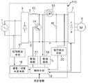
図1は本実施の形態1における電源装置100の構成図を示している。本実施の形態1で説明する電源装置100は例えば空気調和装置の圧縮機に内蔵されるモータや送風ファンのモータなどを駆動するための電源に使用されるものである。
電源装置100は外部電源である交流電源1からの突入電流を防止する突入電流防止回路2と、交流電源1から供給される交流電流を整流する整流回路3と、整流回路3で整流された電流を昇圧して直流電流に変換する昇圧チョッパ回路4を備えている。
整流回路3の高電圧側に出力端には高圧側母線5が、その低電圧側の出力端には低圧側母線6が接続されている。整流回路3と昇圧チョッパ回路4は交流電流を直流電流に変換するコンバータ部であって、直流に変換された電流は昇圧チョッパ回路4から負荷側であるインバータ7に供給され、直流電流はインバータ7で任意の周波数の三相の交流電流に変換される。インバータ7で直流電流から三相交流電流に変換された電流はインバータ7に接続されたモータ8へと流れ、モータ8を駆動する。モータ8は例えば空気調和装置の圧縮機や送風ファンのモータなどである。
FIG. 1 shows a configuration diagram of a
The
A high
突入電流防止回路2は、抵抗9と双方向スイッチ10を備えている。抵抗9と双方向スイッチ10は並列に接続されており、双方向スイッチ10がオン制御されて、交流電流が双方向スイッチ10を導通している場合はほぼすべての電流は双方向スイッチ10を流れ、双方向スイッチ10がオフ制御されて非導通となっている場合はすべての電流は抵抗9を流れる。
双方向スイッチ10は、スイッチング素子を有し、そのスイッチング素子がオン/オフすることにより、電源側接点11と整流回路側接点12の間の交流電流の導通/非導通が切り替わる構成となっている。双方向スイッチ10の具体的な構成については図3、4を用いて後述する。
The inrush
The
整流回路3は、例えば4つのダイオードがブリッジ状に設けられたダイオードブリッジであり、交流電源1から流れる交流電流を整流して負荷側に供給する。
The
昇圧チョッパ回路4は、コイル13とスイッチング素子14とダイオード15と平滑コンデンサ16を備えている。コイル13は整流回路3の高圧側の高圧側母線5上に整流回路3の高圧側の出力端と直列に接続されており、コイル13と直列にダイオード15が設けられている。ダイオード15はアノードがコイル13と接続し、カソードがインバータ7に接続している。コイル13とダイオード15の間の高圧側母線5から低圧側母線6を接続する配線上にスイッチング素子14が設けられている。スイッチング素子14は例えば、IGBT(絶縁ゲート形バイポーラトランジスタ)などである。平滑コンデンサ16は、ダイオード15とインバータ7の間の高圧側母線5から低圧側母線6を接続する配線上に設けられている。尚、低圧側母線6は接地されてグランド電位となっている。
昇圧チョッパ回路4は、スイッチング素子14がオン状態の間にコイル13はエネルギーを蓄積し、スイッチング素子14がオフした時にコイル13から発生する逆起電力を利用してダイオード15を介して平滑コンデンサ16を充電する。交流電源1から供給される交流電流は整流回路3と昇圧チョッパ回路4で昇圧及び平滑化された直流電流となってインバータ7へ流れる。
The step-
In the step-
電源装置100は、交流電源1から整流回路3に印加される交流電圧の位相を検出する位相検出手段17と、位相検出手段17が検出した位相から交流電源1から交流電流が通電しているか若しくは停電したかを判定する通電/停電判定手段18と、平滑コンデンサ16の両端電圧つまり高圧側母線5と低圧側母線6の電位差を検出する電圧検出手段20と、通電/停電判定手段18の判定結果或いは電圧検出手段20の検出値から双方向スイッチ10、スイッチング素子14、インバータ7を制御する制御手段19を備えており、制御手段19から出力される制御信号に基づいて双方向スイッチ10をオン/オフ駆動する駆動回路21と、スイッチング素子14をオン/オフ駆動する駆動回路22も備えている。
The
位相検出手段17は、交流電源1の正側と負側の電位差を検出し、その検出値を通電/停電判定手段18に出力している。さらに位相検出手段17はその電位差が正から負に、若しくは負から正に変化する時に電位差(交流電圧値)がゼロとなる瞬間をゼロクロスとして検出する。
通電/停電判定手段18は、位相検出手段17から入力された検出値に基づいて、以下の3パターンの判定を行ない、その判定結果を制御手段19に出力する。
(1)交流電源1が停電した否か。
(2)交流電源1から整流回路3に流れる交流電流の通電が再開したか否か。
(3)交流電源1の交流電圧値がゼロクロスしたか否か。
制御手段19は、通電/停電判定手段18から入力された判定結果に基づいて双方向スイッチ10の駆動制御を行なう。制御手段19の制御方法の詳細については図6を用いて後述する。
The
The energization / power
(1) Whether the AC
(2) Whether energization of the alternating current flowing from the alternating
(3) Whether or not the AC voltage value of the
The control means 19 performs drive control of the
通電/停電判定手段18が行なう判定方法について、図2を用いて説明する。図2は上段の図2(a)には時間tと交流電圧Vの関係、下段の図2(b)には時間tと双方向スイッチ10のオン/オフのタイミングの関係を示している。図2(a)において横軸は時間t、縦軸は交流電源1が整流回路3に印加する交流電圧の電圧Vであり、図2(b)において横軸が時間t、縦軸が双方向スイッチ10のオン/オフを示している。尚、図2では、時間t=t1で停電により交流電源1からの電力の供給が停止し、時間t=t2で交流電源1が復電して交流電源1から電力の供給が再開したものとする。時間t=t3では電源の復電後の1回目に交流電圧Vがゼロクロスした時である。また、時間t1における交流電圧VをV1、時間t2における交流電圧VをV2とする。
A determination method performed by the energization / power failure determination means 18 will be described with reference to FIG. 2A shows the relationship between the time t and the AC voltage V in FIG. 2A in the upper stage, and FIG. 2B shows the relationship between the time t and the ON / OFF timing of the
時間t1で停電すると、交流電圧VがV1から0Vに一瞬で変化する。位相検出手段17は所定時間間隔(Δt)毎の交流電圧Vの変化量ΔVを通電/停電判定手段18に出力し、通電/停電判定手段18は位相検出手段17から入力されるΔVが所定値以上であり、変化後の交流電圧V≒0であれば停電したと判断することができる。
時間t2で交流電源1が停電から復電すると、交流電圧Vは0VからV2に一瞬で変化する。通電/停電判定手段18は位相検出手段17から入力された変化量ΔVが所定値以上であり、変化前の交流電圧V=0であれば停電から復電したと判断することができる。
また、通電/停電判定手段18は所定時間Δtの前後で交流電圧Vの正負が反転し、ΔVの値が所定値未満であれば交流電圧がゼロクロスしたと判断することができる。
When a power failure occurs at time t1, the AC voltage V changes from V1 to 0V in an instant. The phase detection means 17 outputs the change amount ΔV of the AC voltage V every predetermined time interval (Δt) to the energization / power failure determination means 18, and the energization / power failure determination means 18 determines that ΔV input from the phase detection means 17 is a predetermined value. As described above, if the changed AC voltage V≈0, it can be determined that a power failure has occurred.
When
Further, the energization / power failure determination means 18 can determine that the AC voltage has zero-crossed if the polarity of the AC voltage V is reversed before and after the predetermined time Δt and the value of ΔV is less than the predetermined value.
制御手段19は、通電/停電判定手段18が位相検出手段17の検出値に基づいて交流電源1が停電したと判定した信号を受け取ると直ちに双方向スイッチ10を非導通にする信号を駆動回路21に出力し、駆動回路21はその信号に基づいて双方向スイッチ10を非導通にする。双方向スイッチ10が非導通になると、時間t2で交流電源1が復電して通電が再開した時に電流が抵抗9を流れるので整流回路3等の素子に突入電流が流れることを防止することができる。
As soon as the control means 19 receives a signal determined by the energization / power failure determination means 18 that the
また、制御手段19は交流電源1が復電した後交流電圧がゼロクロスするまでは双方向スイッチ10を導通にせず非導通の状態を維持する制御を行ない、交流電圧がゼロクロスした時(時間t3)から双方向スイッチ10を導通にする制御を行なう。つまり、時刻t1から時刻t3までの間は双方向スイッチ10はオフ制御されている。
Further, the control means 19 performs control to maintain the non-conductive state without turning on the
交流電源1が復電するタイミングによっては交流電圧V2は変動する。例えば、交流電源1が復電した時に交流電圧V2の絶対値が最大値となる場合も想定される。このような場合、時間t2で交流電源1が復電した直後では抵抗9の両端に大きな電圧差が生じているので、通電/停電判定手段18が時間t2で双方向スイッチ10を導通にすると、双方向スイッチ10及び整流回路3に突入電流が流れてしまう可能性がある。本実施の形態1では、時間t2の瞬間は双方向スイッチ10は非導通となっており、抵抗9を介して整流回路3に交流電力を供給し、時間t3から双方向スイッチ10を導通にするので、交流電源1の復電時の突入電流の発生を防止することができる。
The AC voltage V2 varies depending on the timing at which the
尚、本実施の形態1においては時間t3で交流電圧がゼロクロスした時から双方向スイッチ10を導通にする制御を行なうと説明したが、双方向スイッチ10を導通にするタイミングは厳密にゼロクロスした瞬間にのみ限定するものではなく、ゼロクロス近傍であればよく、ゼロクロスした瞬間及びその前後の微小時間を含むものとする。すなわち、ゼロクロスした瞬間を含む所定の時間間隔の間に双方向スイッチ10を導通したときに突入電流が流れなければよい。また、双方向スイッチ10を導通するタイミングは復電後1回目にゼロクロスしたときに限定するものではなく、2回目以降のゼロクロスであってもよい。
In the first embodiment, it has been described that the
尚、制御手段19には外部で設定された設定情報、モータ8の回転数などの情報が入力される。設定情報は、例えば、使用者等が設定した室温、風量等の情報のことである。制御手段19は入力されたモータの回転数から設定情報を満たすように、目標とするモータ8の回転数を算出し、そのモータ8がその目標回転数を達成できるようにスイッチング素子14及びインバータ7のデューティ比や駆動周波数などを制御する。
Note that information such as setting information set externally and the number of revolutions of the motor 8 is input to the control means 19. The setting information is information such as room temperature and air volume set by the user or the like, for example. The control means 19 calculates the target rotational speed of the motor 8 so as to satisfy the setting information from the input rotational speed of the motor, and the switching
ここで、双方向スイッチ10の具体的な構造について図3、図4を用いて説明する。図3は双方向スイッチ10の一形態を示し、図4は双方向スイッチ10の別の形態を示している。
図3に図示する双方向スイッチ10は、ダイオードブリッジ23とMOSFET28を有している。MOSFETとはMetal Oxide Semiconductor Field Effect Transistorのことであり、スイッチング素子の一種である。ダイオードブリッジ23は4つのダイオード24、ダイオード25、ダイオード26、ダイオード27から構成されるダイオードブリッジである。
電源側接点11と接続した点aとダイオード24のアノードが接続されており、ダイオード24のカソードとダイオード25のカソードが点bで接続している。また、ダイオード24のアノードはダイオード27のカソードと点aで接続している。ダイオード25のアノードはダイオード26のカソードと点cで接続し、点cは整流回路側接点12と接続している。ダイオード26のアノードとダイオード27のアノードは点dで接続している。
点bと点dはMOSFET28を介して接続し、MOSFET28はP型であって、そのドレイン電極が点bと接続し、MOSFET28のソース電極が点dと接続している。そしてMOSFET28のゲート電極に駆動回路21から出力される信号がゲート電圧として印加される。
電源側接点11から整流回路側接点12に電流が流れる場合、電源側接点11、点a、ダイオード24、点b、MOSFET28、点d、ダイオード26点c、整流回路側接点12の順に電流が流れる。また、整流回路側接点12から電源側接点11に電流が流れる場合、整流回路側接点12、点c、ダイオード25、点b、MOSFET28、点d、ダイオード27、点a、電源側接点11の順に電流が流れる。
制御手段19はMOSFET28をオン/オフすることにより双方向スイッチ10の導通/非導通を制御することができる。
Here, a specific structure of the
The
The point a connected to the power
The point b and the point d are connected via the
When a current flows from the power
The control means 19 can control conduction / non-conduction of the
図4に図示する双方向スイッチ10は、2つのダイオード29、30及び2つのMOSFET31、32を有している。MOSFET31、32はともにP型である。MOSFET31のソース電極は電源側接点11と接続し、MOSFET31のドレイン電極はダイオード29のカソードと接続している。ダイオード29のアノードは整流回路側接点12と接続し、MOSFET32のソース電極も整流回路側接点12と接続している。MOSFET32のドレイン電極はダイオード30のカソードと接続し、ダイオード30のアノードは電源側接点11と接続している。
電源側接点11から整流回路側接点12に電流が流れる場合、電源側接点11、ダイオード30、MOSFET32、整流回路側接点12の順に電流が流れる。整流回路側接点12から電源側接点11に電流が流れる場合、整流回路側接点12、ダイオード29、MOSFET31、電源側接点11の順に電流が流れる。
MOSFET31のゲート電極及びMOSFET32のゲート電極には駆動回路21から出力される信号がゲート電圧として印加される。
制御手段19は電源側接点11から整流回路側接点12に電流が流れている場合は、MOSFET32をオン/オフし、整流回路側接点12から電源側接点11に電流が流れている場合はMOSFET31をオン/オフすることによって双方向スイッチ10の導通/非導通を制御することができる。
The
When a current flows from the power
A signal output from the
The control means 19 turns on / off the
本実施の形態1において双方向スイッチ10が有しているスイッチング素子、すなわちMOSFET28、MOSFET31、MOSFET32は、ワイドバンドギャップ半導体、特にシリコンカーバイド(以下、SiC)を使用したMOSFET素子である。
The switching elements included in the
ワイドバンドギャップ半導体とは、シリコン(Si)よりもバンドギャップが大きい半導体の総称のことであり、SiC、窒化ガリウム(GaN)、ダイヤモンドなどの半導体が当てはまる。特にSiCはバンドギャップが3.25eVとSiよりも約3倍大きい。これらワイドバンドギャップ半導体を使用したスイッチング素子はSiを使用したスイッチング素子より高いキャリア周波数(25kHz以上)でスイッチング可能であり、さらに通電時のオン抵抗も小さく、耐熱温度も高い。SiCは絶縁破壊電界強度が3MV/cmとSiよりも約10倍大きい。このことからSiC−MOSFETの場合、そのSiCのエピタキシャル層(半導体層)をSiに比べて大幅に薄くすることができ、さらにキャリア濃度も高めることができるので、低損失で高速なスイッチングが可能となる。 The wide band gap semiconductor is a general term for semiconductors having a band gap larger than that of silicon (Si), and semiconductors such as SiC, gallium nitride (GaN), and diamond are applicable. In particular, SiC has a band gap of 3.25 eV, which is about three times larger than Si. Switching elements using these wide bandgap semiconductors can be switched at a higher carrier frequency (25 kHz or more) than switching elements using Si, and also have low on-resistance and high heat resistance when energized. SiC has a dielectric breakdown field strength of 3 MV / cm, which is about 10 times larger than Si. Therefore, in the case of a SiC-MOSFET, the SiC epitaxial layer (semiconductor layer) can be made much thinner than Si, and the carrier concentration can be increased, so that high-speed switching with low loss is possible. Become.
図5は停電から復電した時の双方向スイッチ10の動作を示している。図5(a)は図2(a)と同様に時間tと交流電圧Vの関係を示しており、横軸は時間t、縦軸は交流電源1が整流回路3に印加する交流電圧の電圧Vである。図5においても図2と同様に、時間t=t1で停電により交流電源1からの電力の供給が停止し、時間t=t2で電源が復電して交流電源1から電力の供給が再開したものとする。時間t=t3では電源の復電後の1回目に交流電圧Vがゼロクロスした時である。
図5(b)及び図5(c)は時間tと双方向スイッチ10のオン/オフの関係を示している。図5(b)及び図5(c)では、図2(b)の場合と同様に時間t1で双方向スイッチ10をオフにして非導通とする。しかし、時間t3からは、図2(b)の場合と異なり、双方向スイッチ10をPWM(Pulse Width Modulation)制御する。
図5(b)には、時間t3からキャリア周波数一定で双方向スイッチ10をスイッチングさせる場合を図示している。図5(b)では時間t3から所定時間、若しくは電圧検出手段20の検出値が所定値に達するまで、25〜60kHzの任意の周波数で双方向スイッチ10をスイッチングしている。
図5(c)には、時刻t3からキャリア周波数を時間が経つにつれて小さくしてスイッチングさせる場合を図示している。図5(c)では時間t3から所定時間、若しくは電圧検出手段20の検出値が所定値に達するまで、25〜60kHzの間の任意の周波数で双方向スイッチ10のスイッチングを開始し、終了時には25kHz未満の周波数で双方向スイッチ10のスイッチングを終了している。
FIG. 5 shows the operation of the
FIGS. 5B and 5C show the relationship between the time t and the on / off state of the
FIG. 5B shows a case where the
FIG. 5C illustrates a case where switching is performed with the carrier frequency decreased from time t3 as time passes. In FIG. 5C, switching of the
本実施の形態1では、双方向スイッチ10が有するスイッチング素子にSiC−MOSFETを使用しているので、Siを使用したスイッチング素子、例えばSi−IGBTが可能なキャリア周波数よりも大きい周波数(25kHz以上)でスイッチングが可能となる。SiC−MOSFETを使用し、時間t3から高い周波数でスイッチングさせることにより、平滑コンデンサ16にかかる負荷を下げることができ、平滑コンデンサ16の使用寿命を延ばすことができる。また、時間t3から時間が経つにつれてキャリア周波数を下げることによりスイッチング損失を低減することができる。
尚、図5(b)及び図5(c)ではデューティ比一定で双方向スイッチ10をスイッチングさせる場合を図示しているが、時間が経つにつれて段階的若しくは連続的にデューティ比を大きくしてスイッチングさせてもよい。
In this
5B and 5C show the case where the
ここまで交流電源1の復電時の双方向スイッチ10の動作について説明したが、交流電源1の停電時の双方向スイッチ10の動作についても説明する。
交流電源1が停電してから双方向スイッチ10が非導通となるまでの間に遅延時間があると、この間に平滑コンデンサ16が放電してその両端電圧が低下してしまう。そして双方向スイッチ10が非導通になる前に交流電源1が復電してしまうと、突入電流が整流回路3に流れてしまう可能性がある。特に双方向スイッチ10に代えてメカニカルリレーを使用する構成であると、リレーを切り離すためには物理的動作が必要となるので、このような問題が顕著になる。
そこで、本発明ではメカニカルリレーの代わりにスイッチング素子を使用した双方向スイッチ10を用いている。双方向スイッチ10の導通/非導通の切り替えをスイッチング素子のオン/オフで行なう、つまり物理的動作ではなく電気的動作で行なうことにより、停電を検出して(時間t1)から双方向スイッチ10を非導通するまでの時間を大幅に短縮することができる。
特に本実施の形態1では双方向スイッチ10にSiC−MOSFETを使用しており、そのメリットは大きい。ここでは、SiC−MOSFETとSi−IGBT、Si−MOSFETを比較してその点について説明する。まず双方向スイッチ10には以下の3つの要件が求められる。
(1)通電時のエネルギーロス(定常損失)が少ないこと。通常運転時は双方向スイッチ10に電流が流れていることから、省エネ性の観点から通電時は当然エネルギーロスが少ないことが望ましい。
(2)スイッチング時のエネルギーロス(スイッチング損失)が少ないこと。復電時に平滑コンデンサ16に与える負荷を小さくするために、復電時は双方向スイッチ10をスイッチングさせながら平滑コンデンサ16を充電することが望ましい。
(3)応答速度が速いこと。停電時に双方向スイッチ10が非導通になる前に復電すると突入電流が発生する可能性があることから、双方向スイッチ10の応答速度は速いことが望ましい。
The operation of the
If there is a delay time between the
Therefore, in the present invention, the
In particular, the first embodiment uses a SiC-MOSFET for the
(1) There is little energy loss (steady loss) during energization. Since current flows through the
(2) There is little energy loss (switching loss) at the time of switching. In order to reduce the load applied to the smoothing
(3) The response speed is fast. Since a rush current may occur if power is restored before the
上記3つの要件に対して、SiC−MOSFETとSi−IGBT、Si−MOSFETを当てはめると、Si−IGBTは定常損失は小さいが、スイッチング損失が大きく、さらに応答速度が遅い。Si−MOSFETはスイッチング損失は小さいが、定常損失が大きく、さらに応答速度も遅い。これらに対して、SiC−MOSFETはスイッチング損失、定常損失ともに小さく、さらに応答速度も速い。
尚、ここでいう応答速度はキャリア周波数の相関関係があり、キャリア周波数を高くできるスイッチング素子ほど応答速度が速いといえる。
When SiC-MOSFET, Si-IGBT, and Si-MOSFET are applied to the above three requirements, Si-IGBT has a small steady loss, but has a large switching loss and a slow response speed. Si-MOSFET has a small switching loss, but has a large steady loss and a slow response speed. On the other hand, the SiC-MOSFET has a small switching loss and a steady loss, and further has a high response speed.
It should be noted that the response speed here has a correlation with the carrier frequency, and it can be said that the response speed is higher for a switching element capable of increasing the carrier frequency.
このように本実施の形態1では双方向スイッチ10にSiC−MOSFETを使用しているので、以上の3つの要件を満たし、省エネ性及び瞬時停電に対する信頼性の高めることができる。
Thus, in this
ここで、図7のフローチャートを用いて電源装置100の制御方法について詳細に説明する。
ステップ1(以下、ステップをSと略す)では、使用開始時に使用者が交流電源1を投入する。交流電源1が交流電圧を電源装置100に印加し、S2に進む。最初に交流電源1の投入した時は、平滑コンデンサ16は充電されておらず、双方向スイッチ10が導通状態となっていると、突入電流が整流回路3等の素子に流れるおそれがある。そこで、S2では、通電開始直後は制御手段19が駆動回路21に制御信号を出力し双方向スイッチ10を非導通状態となるように制御している。その後S3に進む。
S3では、l1lは位相検出手段17の出力値から交流電圧がゼロクロスしたか否かを判定する。ゼロクロスしたと判定した場合はS4に進み、ゼロクロスしていないと判定した場合はS3をループする。
S4では、交流電圧がゼロクロスした時から双方向スイッチ10を導通状態にして、交流電流を双方向スイッチ10に流して平滑コンデンサ16の充電し、モータ8の駆動を開始する。その後S5に進む。
S5では、モータ8の運転を継続するか否かを制御手段19が判定する。運転を継続しない場合はS6に進む。運転を継続しない場合とは、例えば使用者が装置の運転止める信号を制御手段19に入力した場合など、制御手段19はその入力された信号に基づいてS6でモータ8の運転を停止する。運転を継続する場合はそのままS7に進む。
S7では、通電/停電判定手段18が位相検出手段17の出力値に基づいて停電が発生したか否かを判定する。停電が発生したと判定した場合はS8に進み、停電が発生していないと判定した場合はS5に戻る。尚、停電が発生した否かの判定は上述した方法にて行なうものとする。
S8では、制御手段19は双方向スイッチ10を非導通とする制御信号を駆動回路21に出力し、双方向スイッチ10を非導通状態とする。その後S9に進む。
S9では、通電/停電判定手段18が位相検出手段17の出力値から交流電源1が停電から復電したか否かを判定する。停電から復電していないと判定した場合はS9をループし、停電から復電したと判定した場合はS3に戻る。尚、停電から復電したか否かの判定は上述した方法にて行なうものとする。
Here, the control method of the
In step 1 (hereinafter, step is abbreviated as S), the user turns on the
In S3, l11 determines from the output value of the
In S4, the
In S5, the control means 19 determines whether or not to continue the operation of the motor 8. If the operation is not continued, the process proceeds to S6. The case where the operation is not continued means that, for example, when the user inputs a signal for stopping the operation of the apparatus to the control means 19, the control means 19 stops the operation of the motor 8 in S6 based on the input signal. If the operation is continued, the process proceeds to S7 as it is.
In S <b> 7, the energization / power failure determination means 18 determines whether or not a power failure has occurred based on the output value of the phase detection means 17. If it is determined that a power failure has occurred, the process proceeds to S8. If it is determined that a power failure has not occurred, the process returns to S5. Note that the determination as to whether or not a power failure has occurred is made by the method described above.
In S8, the control means 19 outputs a control signal for making the
In S <b> 9, the energization / power
このように、通電開始時及び停電復電後の直後はS2とS8でそれぞれ双方向スイッチ10を非導通する制御を行なっているので、交流電源1が投入、復電した直後は交流電流は抵抗9を流れるので、どのタイミングで交流電源1が投入、復電したとしても突入電流が生じることがない。さらに、交流電源1が投入、復電した後ゼロクロスを検出し、ゼロクロスした瞬間若しくはその前後から双方向スイッチ10を導通する制御を行なうようにしているので、双方向スイッチ10を導通した瞬間に突入電流の発生を防止することができる。
As described above, since the
実施の形態2.
実施の形態1では交流電源1から整流回路3の間の交流電流が流れる線に双方向スイッチ10を設ける構成の電源装置100について説明した。本実施の形態2では双方向スイッチ10に代えてコイル13より負荷側の直流電流が流れる配線上にスイッチング素子を設ける構成の電源装置110、120について説明する。尚、本実施の形態2において実施の形態1と同一の構成部分には同一の符号を付し説明は省略する。
In the first embodiment, the
図7には、本実施の形態2の電源装置110の回路図を示している。電源装置110はコイル13より負荷側の高圧側母線5上にスイッチング素子であるP型のP−MOSFET33を備えている。P−MOSFET33はソース電極がコイル13と直列に接続されており、ドレイン電極が平滑コンデンサ16及びインバータ7の高圧側端子と接続されている。制御手段19は駆動回路21に代えて設けられた駆動回路34に制御信号を出力する。さらに駆動回路34にはP−MOSFET33のソース電位が入力される。P−MOSFET33のゲート電極は駆動回路34に接続されており、駆動回路34から出力される駆動信号がゲート電圧としてP−MOSFET33のゲート電極に印加される。
スイッチング素子14は、コイル13とP−MOSFET33の間の高圧側母線5と低圧側母線6を繋ぐ配線上に設けられている。
FIG. 7 shows a circuit diagram of the
The switching
図8には、本実施の形態2における別の形態の電源装置120の回路図を示している。電源装置120は低圧側母線6上にN型のN−MOSFET35を備えている。N−MOSFET35はソース電極がグランドに接続されており、ドレイン電極が平滑コンデンサ16及びインバータ7の低圧側端子と接続されている。制御手段19は駆動回路21に代えて設けられた駆動回路36に制御信号を出力する。P−MOSFETのゲート電極は駆動回路36に接続されており、駆動回路36から出力される駆動信号がゲート電圧としてN−MOSFET35のゲート電極に印加される。駆動回路36はグランド電位を基準にしてゲート電圧を出力している。
FIG. 8 shows a circuit diagram of another form of
制御手段19はP−MOSFET33とN−MOSFET35を実施の形態1の双方向スイッチ10と同様に制御するものとする。つまり、ll2の判定結果に基づいて制御手段19はP−MOSFET33とN−MOSFET35を制御する。実施の形態1の図6のフローチャート図で説明すると、S7で通電/停電判定手段18が停電が発生したと判定するとS8で制御手段19はP−MOSFET33、N−MOSFET35をオフにする制御を行なう。そしてS9で電源が復電したと通電/停電判定手段18が判定するとS3に戻り、S3で交流電圧のゼロクロスを検出すると、S4で制御手段19がP−MOSFET33、N−MOSFET35をオンにする。S4でP−MOSFET33、N−MOSFET35をオンにする際、図5で上述したようにスイッチングさせてもよい。また、S1で運転開始時に交流電源1を投入する場合は、S3を飛ばしてS2からS4に進んでも良い。
本実施の形態2では、P−MOSFET33とN−MOSFET35をSiC−MOSFETとしているので、実施の形態1で既に説明したように25〜60kHzのキャリア周波数でスイッチング可能であり、平滑コンデンサ16の充電時に平滑コンデンサ16にかかる負荷を低減することができる。
The control means 19 controls the P-
In the second embodiment, since the P-
さらに、電源装置110では、高圧側母線5上に設けたスイッチング素子をP型のMOSFET33としたことにより、コンバータ側からの電位、つまりソース電圧を基準にして駆動回路34がゲート電圧を出力することができるので、P−MOSFET33のゲート電圧を作る際に別途絶縁電源を設ける必要がなくなる。
同様に電源装置120では、低圧側母線6上に設けたスイッチング素子をN型のMOSFET35としたことにより、グランド電位であるソース電圧を基準にして駆動回路36がゲート電圧出力することができので、N−MOSFET35のゲート電圧を作る際に別途絶縁電源を設ける必要がなくなる。
Further, in the
Similarly, in the
実施の形態3.
図9は、本実施の形態3における空気調和装置200の構成図である。空気調和装置200は実施の形態1、2で説明した電源装置100、110、120のいずれかの電源装置を備えている。本実施の形態3では電源装置100を備えているものとして説明する。
FIG. 9 is a configuration diagram of the air-
空気調和装置200は、室外に設置される室外機37と空調の対象となる室内空間に設置される室内機38とで構成されている。
室外機37には、冷媒を圧縮して吐出する圧縮機39と、圧縮機39から吐出された冷媒の流れる方向を暖房運転と冷房運転に応じて切り替える四方弁40が設けられている。四方弁40には4つの接続部があり、1つは圧縮機39の冷媒の吐出配管と接続し、1つは圧縮機39の冷媒の吸入配管と接続し、1つは圧縮機39に設けられた熱源側熱交換器41と接続し、1つは室内機38に設けられた負荷側熱交換器42と接続している。熱源側熱交換器41と負荷側熱交換器42の間には冷媒を減圧する膨張弁43が設けられている。また、室外機37には熱源側熱交換器41に室外空気を送風する室外送風機44が設けられている。室内機38には負荷側熱交換器42と、負荷側熱交換器42に室内空気を送風する室内送風機45とが設けられている。
The
The
室外機37には交流電源1から供給される交流電流を直流に変換する電源装置100と、電源装置100が変換した直流電流を3相の交流電流に変換するインバータ7を備えた制御基板46を備えている。インバータ7で変換された3相交流電流は制御基板46から圧縮機39の内部で冷媒を圧縮する駆動部を駆動するモータ8に供給される。モータ8にはモータ8の回転数を検出する手段が設けられており、検出された回転数は制御基板46の制御手段19に出力される。
室内機38が設置されている室内にはリモコン47が設けられており、使用者はリモコン47で冷房運転、暖房運転や室内の設定温度などの運転情報を設定することができ、リモコン47で設定された情報は制御手段19に出力される。
制御手段19は入力されたモータ8の回転数、電圧検出手段20の検出値、リモコン47で設定された運転情報に基づいて双方向スイッチ10、スイッチング素子14、インバータ7を制御する。
The
A
The control means 19 controls the
以上のように、本実施の形態3の空気調和装置200は実施の形態1、2で説明した電源装置100、110、120のいずれかの電源装置を備えているので、交流電源1の瞬停時の突入電流の発生を防止することができ、突入電流に対する装置の信頼性を向上させることできる。
As described above, the air-
尚、本実施の形態3では、電源装置100とインバータ7で変換した交流電流を圧縮機39のモータ8に供給する構成について説明した。しかし、モータ8は圧縮機39に使用するものに限定するわけではなく、室外送風機44や室内送風機45に使用するモータであってもよい。
In the third embodiment, the configuration in which the alternating current converted by the
本発明は交流電流を直流電流に変換する電源装置に利用することができる。 The present invention can be used in a power supply device that converts alternating current into direct current.
1 交流電源、 2 突入電流防止回路、 3 整流回路、4 昇圧チョッパ回路、 5 高圧側母線、 6 低圧側母線、 7 インバータ、 8 モータ、 9 抵抗、 10 双方向スイッチ、 11 電源側接点、 12 整流回路側接点、 13 コイル、 14 スイッチング素子、 15 ダイオード、 16 平滑コンデンサ、 17 位相検出手段、 18 通電/停電判定手段、 19 制御手段、 20 電圧検出手段、 21 駆動回路、 22 駆動回路、 23 ダイオードブリッジ、 24、25、26、27 ダイオード、 28 MOSFET、29、30 ダイオード、 31 MOSFET、 32 MOSFET、 33 P−MOSFET、 34 駆動回路、 35 N−MOSFET、 36 駆動回路、 37 室外機、 38 室内機、 39 圧縮機、 40 四方弁、 41 熱源側熱交換器、 42 負荷側熱交換器、 43 膨張弁、 44 室外送風機、 45 室内送風機、 46 制御基板、 47 リモコン、 100、110、 120 電源装置、 200 空気調和装置。
1 AC power supply, 2 Inrush current prevention circuit, 3 Rectifier circuit, 4 Boost chopper circuit, 5 High voltage side bus, 6 Low voltage side bus, 7 Inverter, 8 Motor, 9 Resistance, 10 Bidirectional switch, 11 Power supply side contact, 12 Rectification Circuit side contact, 13 coil, 14 switching element, 15 diode, 16 smoothing capacitor, 17 phase detection means, 18 energization / power failure determination means, 19 control means, 20 voltage detection means, 21 drive circuit, 22 drive circuit, 23
Claims (9)
前記交流電源から前記整流回路に印加される交流電圧の位相を検出する位相検出手段と、
前記交流電源と前記整流回路の間に設けられ、前記交流電源から前記整流回路及び前記整流回路から前記交流電源の双方向に通電可能な双方向スイッチと、
前記双方向スイッチと並列に設けられた抵抗と、
前記整流回路が整流した電流を平滑化して負荷側に供給する平滑コンデンサと、
前記位相検出手段が検出した位相に基づいて前記交流電流の通電が停止したか否か及び前記交流電流の通電が再開したか否かを判定する判定手段と、
前記判定手段が前記交流電流の通電が停止したと判定すると前記双方向スイッチがオフになる制御をし、前記判定手段が前記交流電流の通電が再開したと判定すると前記位相検出手段が検出する前記交流電圧のゼロクロス近傍で前記双方向スイッチがオンになる制御をする制御手段と、
を備えた電源装置。 A rectifier circuit for rectifying an alternating current supplied from an alternating current power supply;
Phase detection means for detecting the phase of an AC voltage applied to the rectifier circuit from the AC power supply;
A bidirectional switch provided between the AC power supply and the rectifier circuit, capable of energizing bidirectionally from the AC power supply to the rectifier circuit and from the rectifier circuit to the AC power supply;
A resistor provided in parallel with the bidirectional switch;
A smoothing capacitor that smoothes the current rectified by the rectifier circuit and supplies it to the load side;
Determining means for determining whether or not energization of the alternating current is stopped and whether or not energization of the alternating current is restarted based on the phase detected by the phase detecting means;
The bi-directional switch is controlled to be turned off when the determination unit determines that the energization of the alternating current is stopped, and the phase detection unit detects when the determination unit determines that the energization of the alternating current is resumed. Control means for controlling the bidirectional switch to be turned on near the zero cross of the AC voltage;
Power supply unit with
前記制御手段は前記MOSFET素子のオンとオフを制御することにより前記双方向スイッチがオンになる制御とオフになる制御を切り替えることを特徴とする請求項1に記載の電源装置。 The bidirectional switch has a MOSFET element using a wide band gap semiconductor,
2. The power supply device according to claim 1, wherein the control unit switches between control for turning on and off the bidirectional switch by controlling on and off of the MOSFET element.
前記交流電源から前記整流回路に流れる交流電圧の位相を検出する位相検出手段と、
前記整流回路が整流した電流を平滑化して負荷側に供給する平滑コンデンサと、
前記整流回路と前記負荷側を繋ぐ高圧側の配線に設けられ、ソースが前記整流側にドレインが前記負荷側に接続されたP型のMOSFET素子と、
前記位相検出手段が検出した位相に基づいて前記交流電流の通電が停止したか否か及び前記交流電流の通電が再開したか否かを判定する判定手段と、
前記判定手段が前記交流電流の通電が停止したと判定すると前記MOSFET素子をオフになる制御をし、前記判定手段が前記交流電流の通電が再開したと判定すると前記位相検出手段が検出する前記交流電圧のゼロクロス近傍で前記MOSFET素子がオンになる制御をする制御手段と、
を備えた電源装置。 A rectifier circuit for rectifying an alternating current supplied from an alternating current power supply;
Phase detection means for detecting the phase of an AC voltage flowing from the AC power supply to the rectifier circuit;
A smoothing capacitor that smoothes the current rectified by the rectifier circuit and supplies it to the load side;
A P-type MOSFET element provided on a high-voltage side wiring connecting the rectifier circuit and the load side, a source connected to the rectifier side and a drain connected to the load side;
Determining means for determining whether or not energization of the alternating current is stopped and whether or not energization of the alternating current is restarted based on the phase detected by the phase detecting means;
When the determination means determines that the supply of the alternating current is stopped, the MOSFET element is controlled to be turned off. When the determination means determines that the supply of the alternating current is resumed, the alternating current detected by the phase detection means is detected. Control means for controlling the MOSFET element to be turned on in the vicinity of the zero cross of the voltage;
Power supply unit with
前記交流電源から前記整流回路に流れる前記交流電流の位相を検出する位相検出手段と、
前記整流回路が整流した電流を平滑化して負荷側に供給する平滑コンデンサと、
前記整流回路と前記負荷側を繋ぐ低圧側の配線に設けられ、ソースが前記整流側にドレインが前記負荷側に接続されたN型のMOSFET素子と、
前記位相検出手段が検出した位相に基づいて前記交流電流の通電が停止したか否か及び前記交流電流の通電が再開したか否かを判定する判定手段と、
前記判定手段が前記交流電流の通電が停止したと判定すると前記MOSFET素子をオフになる制御をし、前記判定手段が前記交流電流の通電が再開したと判定すると前記位相検出手段が検出する前記交流電圧のゼロクロス近傍で前記MOSFET素子がオンになる制御をする制御手段と、
を備えた電源装置。 A rectifier circuit for rectifying an alternating current supplied from an alternating current power supply;
Phase detection means for detecting the phase of the alternating current flowing from the alternating current power source to the rectifier circuit;
A smoothing capacitor that smoothes the current rectified by the rectifier circuit and supplies it to the load side;
An N-type MOSFET element provided on a low-voltage side wiring connecting the rectifier circuit and the load side, a source connected to the rectifier side and a drain connected to the load side;
Determining means for determining whether or not energization of the alternating current is stopped and whether or not energization of the alternating current is restarted based on the phase detected by the phase detecting means;
When the determination means determines that the supply of the alternating current is stopped, the MOSFET element is controlled to be turned off. When the determination means determines that the supply of the alternating current is resumed, the alternating current detected by the phase detection means is detected. Control means for controlling the MOSFET element to be turned on in the vicinity of the zero cross of the voltage;
Power supply unit with
前記電圧検出手段の検出値が上がると前記キャリア周波数を下げることを特徴とする請求6又は7に記載の電源装置。 Voltage detecting means for detecting a voltage across the smoothing capacitor;
The power supply device according to claim 6 or 7, wherein the carrier frequency is lowered when a detection value of the voltage detection means increases.
前記電源装置が変換した直流電流を交流電流に変換するインバータと、
前記インバータが変換した交流電流により駆動されるモータと、
を備えたことを特徴とする空気調和装置。 A power supply device according to any one of claims 1 to 8,
An inverter that converts the direct current converted by the power supply device into an alternating current;
A motor driven by the alternating current converted by the inverter;
An air conditioner comprising:
Priority Applications (1)
| Application Number | Priority Date | Filing Date | Title |
|---|---|---|---|
| JP2011038362A JP5724451B2 (en) | 2011-02-24 | 2011-02-24 | Power supply device and air conditioner |
Applications Claiming Priority (1)
| Application Number | Priority Date | Filing Date | Title |
|---|---|---|---|
| JP2011038362A JP5724451B2 (en) | 2011-02-24 | 2011-02-24 | Power supply device and air conditioner |
Publications (3)
| Publication Number | Publication Date |
|---|---|
| JP2012175882A JP2012175882A (en) | 2012-09-10 |
| JP2012175882A5 JP2012175882A5 (en) | 2013-08-08 |
| JP5724451B2 true JP5724451B2 (en) | 2015-05-27 |
Family
ID=46978227
Family Applications (1)
| Application Number | Title | Priority Date | Filing Date |
|---|---|---|---|
| JP2011038362A Expired - Fee Related JP5724451B2 (en) | 2011-02-24 | 2011-02-24 | Power supply device and air conditioner |
Country Status (1)
| Country | Link |
|---|---|
| JP (1) | JP5724451B2 (en) |
Families Citing this family (11)
| Publication number | Priority date | Publication date | Assignee | Title |
|---|---|---|---|---|
| CN105075099B (en) * | 2013-10-08 | 2017-09-22 | 富士电机株式会社 | Power conversion device |
| JP6173231B2 (en) | 2014-02-05 | 2017-08-02 | 三菱電機株式会社 | Power converter and air conditioner |
| JP6184391B2 (en) | 2014-11-07 | 2017-08-23 | 三菱電機株式会社 | Air conditioner |
| US10128649B2 (en) | 2015-03-11 | 2018-11-13 | Mistubishi Electric Corporation | Power supply device |
| CN107210682B (en) | 2015-03-31 | 2019-07-19 | 三菱电机株式会社 | Power supply device and conditioner |
| JP2018152925A (en) * | 2015-08-04 | 2018-09-27 | 富士電機株式会社 | Three-level chopper device |
| WO2017195370A1 (en) * | 2016-05-13 | 2017-11-16 | 三菱電機株式会社 | Electrical power converter |
| JP6776046B2 (en) | 2016-07-29 | 2020-10-28 | 株式会社マキタ | Electric work machine |
| CN109936203A (en) * | 2017-12-18 | 2019-06-25 | 奥克斯空调股份有限公司 | A kind of air-conditioning charging circuit, charge control method and air-conditioning with the circuit |
| CN112821350B (en) * | 2020-12-31 | 2023-09-19 | Tcl空调器(中山)有限公司 | Voltage abnormality protection circuit, control method and air conditioner |
| WO2023238229A1 (en) * | 2022-06-07 | 2023-12-14 | 三菱電機株式会社 | Power conversion device, motor drive device, and refrigeration cycle application apparatus |
Family Cites Families (7)
| Publication number | Priority date | Publication date | Assignee | Title |
|---|---|---|---|---|
| JPH04325871A (en) * | 1991-04-26 | 1992-11-16 | Matsushita Refrig Co Ltd | Controller for air conditioner |
| JPH0576135A (en) * | 1991-09-12 | 1993-03-26 | Fuji Electric Co Ltd | Surge current suppressor and suppressing method for uninterruptible power supply |
| JP3301472B2 (en) * | 1995-08-21 | 2002-07-15 | ティアック株式会社 | Circuit device having inrush current prevention function |
| JP2001320882A (en) * | 2000-05-09 | 2001-11-16 | Matsushita Electric Ind Co Ltd | Power supply apparatus, inverter and air conditioner |
| JP2008211683A (en) * | 2007-02-27 | 2008-09-11 | Kyocera Corp | Current control circuit and wireless communication apparatus |
| JP2008252966A (en) * | 2007-03-29 | 2008-10-16 | Matsushita Electric Ind Co Ltd | Motor drive device |
| JP2010161887A (en) * | 2009-01-09 | 2010-07-22 | Panasonic Corp | Power converter and vacuum cleaner using same |
-
2011
- 2011-02-24 JP JP2011038362A patent/JP5724451B2/en not_active Expired - Fee Related
Also Published As
| Publication number | Publication date |
|---|---|
| JP2012175882A (en) | 2012-09-10 |
Similar Documents
| Publication | Publication Date | Title |
|---|---|---|
| JP5724451B2 (en) | Power supply device and air conditioner | |
| AU2011365142B2 (en) | Power converting device, motor driving device, and refrigerating and air-conditioning apparatus | |
| KR101804713B1 (en) | Dc power source device, motor drive device, air conditioner, and refrigerator | |
| AU2011358036B2 (en) | Backflow preventing means, power converting device, and refrigerating and air-conditioning apparatus | |
| US9240737B2 (en) | Control device for switching power supply circuit, and heat pump unit | |
| AU2010361822B2 (en) | Power conversion device and refrigeration air-conditioning device | |
| EP2978117B1 (en) | Electric power conversion device and refrigerating air-conditioning device | |
| US9742267B2 (en) | Power conversion apparatus and refrigeration air-conditioning apparatus | |
| US11101728B2 (en) | Power converting apparatus, motor drive control apparatus, blower, compressor, and air conditioner | |
| JPWO2019026125A1 (en) | Motor drive and refrigeration cycle application equipment | |
| US10928112B2 (en) | Heat pump device | |
| JP2007209166A (en) | Inverter, and refrigeration cycle device | |
| KR101850196B1 (en) | Power conversion device, and cooling air conditioning device | |
| EP3018807B1 (en) | Backflow prevention device, power converter, motor drive device, and refrigerating and air-conditioning device | |
| JP7130568B2 (en) | power supply | |
| WO2022176065A1 (en) | Dc power supply device, motor drive device, and refrigeration cycle application apparatus | |
| US10003184B2 (en) | Backflow preventing device, power conversion device, and refrigeration air-conditioning apparatus | |
| JP2019075907A (en) | Power conversion device, motor driving device, and air conditioner | |
| JP2006149047A (en) | Dc power supply | |
| JP2013143796A (en) | Inverter control circuit and air conditioner using the same |
Legal Events
| Date | Code | Title | Description |
|---|---|---|---|
| A521 | Written amendment |
Free format text: JAPANESE INTERMEDIATE CODE: A523 Effective date: 20130620 |
|
| A621 | Written request for application examination |
Free format text: JAPANESE INTERMEDIATE CODE: A621 Effective date: 20130620 |
|
| A977 | Report on retrieval |
Free format text: JAPANESE INTERMEDIATE CODE: A971007 Effective date: 20140317 |
|
| RD01 | Notification of change of attorney |
Free format text: JAPANESE INTERMEDIATE CODE: A7421 Effective date: 20140326 |
|
| A131 | Notification of reasons for refusal |
Free format text: JAPANESE INTERMEDIATE CODE: A131 Effective date: 20140415 |
|
| TRDD | Decision of grant or rejection written | ||
| A01 | Written decision to grant a patent or to grant a registration (utility model) |
Free format text: JAPANESE INTERMEDIATE CODE: A01 Effective date: 20150303 |
|
| A61 | First payment of annual fees (during grant procedure) |
Free format text: JAPANESE INTERMEDIATE CODE: A61 Effective date: 20150316 |
|
| LAPS | Cancellation because of no payment of annual fees |