EP3091608A1 - Antenna system and antenna module with a parasitic element for radiation pattern improvements - Google Patents
Antenna system and antenna module with a parasitic element for radiation pattern improvements Download PDFInfo
- Publication number
- EP3091608A1 EP3091608A1 EP15166282.2A EP15166282A EP3091608A1 EP 3091608 A1 EP3091608 A1 EP 3091608A1 EP 15166282 A EP15166282 A EP 15166282A EP 3091608 A1 EP3091608 A1 EP 3091608A1
- Authority
- EP
- European Patent Office
- Prior art keywords
- planar
- antenna
- antenna element
- antenna system
- parasitic
- Prior art date
- Legal status (The legal status is an assumption and is not a legal conclusion. Google has not performed a legal analysis and makes no representation as to the accuracy of the status listed.)
- Granted
Links
- 230000003071 parasitic effect Effects 0.000 title claims abstract description 93
- 230000005855 radiation Effects 0.000 title description 10
- 230000006872 improvement Effects 0.000 title description 2
- 230000002829 reductive effect Effects 0.000 claims description 14
- 239000000758 substrate Substances 0.000 claims description 12
- 230000010287 polarization Effects 0.000 claims description 4
- 230000000694 effects Effects 0.000 description 17
- 230000008878 coupling Effects 0.000 description 9
- 238000010168 coupling process Methods 0.000 description 9
- 238000005859 coupling reaction Methods 0.000 description 9
- 238000013461 design Methods 0.000 description 7
- 230000010363 phase shift Effects 0.000 description 5
- 230000009286 beneficial effect Effects 0.000 description 4
- 239000004020 conductor Substances 0.000 description 3
- 238000012986 modification Methods 0.000 description 3
- 230000004048 modification Effects 0.000 description 3
- 230000002411 adverse Effects 0.000 description 2
- 238000010348 incorporation Methods 0.000 description 2
- 230000007774 longterm Effects 0.000 description 2
- 238000010295 mobile communication Methods 0.000 description 2
- 238000013459 approach Methods 0.000 description 1
- 230000003247 decreasing effect Effects 0.000 description 1
- 238000011161 development Methods 0.000 description 1
- 238000006073 displacement reaction Methods 0.000 description 1
- 238000005516 engineering process Methods 0.000 description 1
- 238000005530 etching Methods 0.000 description 1
- 230000002452 interceptive effect Effects 0.000 description 1
- 230000000670 limiting effect Effects 0.000 description 1
- 238000004519 manufacturing process Methods 0.000 description 1
- 238000001465 metallisation Methods 0.000 description 1
- 238000007639 printing Methods 0.000 description 1
- 230000009467 reduction Effects 0.000 description 1
- 230000003252 repetitive effect Effects 0.000 description 1
- 238000000926 separation method Methods 0.000 description 1
Images


Classifications
-
- H—ELECTRICITY
- H01—ELECTRIC ELEMENTS
- H01Q—ANTENNAS, i.e. RADIO AERIALS
- H01Q1/00—Details of, or arrangements associated with, antennas
- H01Q1/52—Means for reducing coupling between antennas; Means for reducing coupling between an antenna and another structure
- H01Q1/521—Means for reducing coupling between antennas; Means for reducing coupling between an antenna and another structure reducing the coupling between adjacent antennas
- H01Q1/523—Means for reducing coupling between antennas; Means for reducing coupling between an antenna and another structure reducing the coupling between adjacent antennas between antennas of an array
-
- H—ELECTRICITY
- H01—ELECTRIC ELEMENTS
- H01Q—ANTENNAS, i.e. RADIO AERIALS
- H01Q1/00—Details of, or arrangements associated with, antennas
- H01Q1/27—Adaptation for use in or on movable bodies
- H01Q1/32—Adaptation for use in or on road or rail vehicles
- H01Q1/325—Adaptation for use in or on road or rail vehicles characterised by the location of the antenna on the vehicle
- H01Q1/3275—Adaptation for use in or on road or rail vehicles characterised by the location of the antenna on the vehicle mounted on a horizontal surface of the vehicle, e.g. on roof, hood, trunk
-
- H—ELECTRICITY
- H01—ELECTRIC ELEMENTS
- H01Q—ANTENNAS, i.e. RADIO AERIALS
- H01Q1/00—Details of, or arrangements associated with, antennas
- H01Q1/52—Means for reducing coupling between antennas; Means for reducing coupling between an antenna and another structure
- H01Q1/521—Means for reducing coupling between antennas; Means for reducing coupling between an antenna and another structure reducing the coupling between adjacent antennas
-
- H—ELECTRICITY
- H01—ELECTRIC ELEMENTS
- H01Q—ANTENNAS, i.e. RADIO AERIALS
- H01Q21/00—Antenna arrays or systems
- H01Q21/28—Combinations of substantially independent non-interacting antenna units or systems
-
- H—ELECTRICITY
- H01—ELECTRIC ELEMENTS
- H01Q—ANTENNAS, i.e. RADIO AERIALS
- H01Q9/00—Electrically-short antennas having dimensions not more than twice the operating wavelength and consisting of conductive active radiating elements
- H01Q9/04—Resonant antennas
- H01Q9/0407—Substantially flat resonant element parallel to ground plane, e.g. patch antenna
- H01Q9/0414—Substantially flat resonant element parallel to ground plane, e.g. patch antenna in a stacked or folded configuration
-
- H—ELECTRICITY
- H01—ELECTRIC ELEMENTS
- H01Q—ANTENNAS, i.e. RADIO AERIALS
- H01Q9/00—Electrically-short antennas having dimensions not more than twice the operating wavelength and consisting of conductive active radiating elements
- H01Q9/04—Resonant antennas
- H01Q9/0407—Substantially flat resonant element parallel to ground plane, e.g. patch antenna
- H01Q9/0421—Substantially flat resonant element parallel to ground plane, e.g. patch antenna with a shorting wall or a shorting pin at one end of the element
-
- H—ELECTRICITY
- H01—ELECTRIC ELEMENTS
- H01Q—ANTENNAS, i.e. RADIO AERIALS
- H01Q9/00—Electrically-short antennas having dimensions not more than twice the operating wavelength and consisting of conductive active radiating elements
- H01Q9/04—Resonant antennas
- H01Q9/0407—Substantially flat resonant element parallel to ground plane, e.g. patch antenna
- H01Q9/0428—Substantially flat resonant element parallel to ground plane, e.g. patch antenna radiating a circular polarised wave
-
- H—ELECTRICITY
- H01—ELECTRIC ELEMENTS
- H01Q—ANTENNAS, i.e. RADIO AERIALS
- H01Q1/00—Details of, or arrangements associated with, antennas
- H01Q1/48—Earthing means; Earth screens; Counterpoises
-
- H—ELECTRICITY
- H01—ELECTRIC ELEMENTS
- H01Q—ANTENNAS, i.e. RADIO AERIALS
- H01Q5/00—Arrangements for simultaneous operation of antennas on two or more different wavebands, e.g. dual-band or multi-band arrangements
- H01Q5/30—Arrangements for providing operation on different wavebands
- H01Q5/307—Individual or coupled radiating elements, each element being fed in an unspecified way
Definitions
- the invention relates to an improved antenna system comprising a first and a second antenna element and a parasitic element where the parasitic element allows for an improvement of the radiation pattern of at least one of the antenna elements. Further, the invention relates to an antenna module incorporating same antenna system.
- an antenna system is to be understood as an antenna arrangement comprising a first antenna element and a second antenna element.
- antenna systems are widely discussed in technology because the grouping of plural antenna elements in one system provides for various structural advantages. Particularly the assembly of an antenna system as a single structural module allows mechanical and electrical components to be shared between the plural antenna elements.
- the plural antenna elements may be arranged within and hence sharing a same housing, a same base, sharing same antenna circuitry, and a same electrically connection element (e.g. socket/plug) for transmitting/receiving electrical signals from the outside to/from the plural antenna elements within the antenna system, respectively.
- a same electrically connection element e.g. socket/plug
- the arrangement of plural antenna elements in an antenna system suffers from disadvantages, particularly when the plural antenna elements are arranged in the near-field to each other.
- the plural antenna elements suffer from mutual interference effects particularly regarding their respective radiating patterns.
- the suggested antenna system comprises a first and a second antenna element.
- the first antenna element is capable of transmitting in a first frequency range
- the second antenna element is capable of transmitting in a second - i.e. non-overlapping - frequency range.
- the antenna system additionally includes a frequency selective surface which is conductive to radio frequency energy in the first frequency range and reflective to radio frequency energy in the second frequency range.
- the frequency selective surface comprises preferably repetitive metallization pattern structures that display quasi band-pass or quasi band-reject filter characteristics to radio frequency signals impinging upon the frequency selective surface.
- US 6,917,340 B2 also relates to an antenna system comprising two antenna elements.
- one of the two antenna elements is subdivided into segments which have an electrical length corresponding to three/eight of the wavelength of the other antenna element.
- the segments of the one antenna element are electrically interconnected via electric reactance circuits which possess sufficiently high impedance in the frequency range of the other antenna element and sufficiently low impedance in the frequency range of the one antenna element.
- the design of the electric reactance circuits and their arrangement on the respective antenna element is complex and necessitates additional development steps. Further the components of the electric reactance circuit as well as the, for instance soldered, electrical connection to the antenna elements introduces unacceptable variances to the frequency characteristic.
- an antenna system comprises a planar parasitic element in addition to a first planar and at least one second antenna element.
- the planar parasitic element allows for the beneficial effect that the interference in-between the first and the second antenna elements of the antenna system is reduced thereby improving the respective radiation patterns.
- an antenna system is proposed comprising a first planar antenna element, and at least one second antenna element, wherein the first planar antenna element and the at least one second antenna element are arranged along an axis.
- the antenna system further comprises a planar parasitic element arranged within the near-field of the first planar antenna element, the planar parasitic element being arranged substantially in parallel to the first planar antenna element and being arranged at a predetermined distance therefrom.
- the center of the planar parasitic element is offset with respect to the center of the first planar antenna element in a direction away from the at least one second antenna element along the axis, so as to reduce a deformation of the radiating pattern of the first planar antenna element due to an interference with the at least one second antenna element.
- each of the at least one second antenna element is arranged within the near-field of the first planar antenna element.
- the first planar antenna element is capable of receiving/transmitting electromagnetic radio waves having a circular polarization.
- the first planar antenna element is a corner-truncated rectangular patch antenna element.
- the size and the shape of the planar parasitic element and the distance thereof from the first planar antenna element are determined in accordance with the first planar antenna element
- the planar parasitic element has no electrical connection to a RF power source.
- the planar parasitic element has a reduced electrical size compared to that of the first planar antenna element determined in accordance with the distance thereof from the first planar antenna element.
- the planar parasitic element has the same shape as the first planar antenna element.
- the distance of the planar parasitic element from the first planar antenna element is between ⁇ /10 and ⁇ /4, where ⁇ corresponds to a wavelength of the first planar antenna element.
- the first planar antenna element is adapted to a first frequency band
- the at least one second antenna element is adapted to a second frequency band, where the first frequency band is higher or equal to the second frequency band.
- the first planar antenna element includes a patch electrode which is provided on a dielectric substrate.
- the planar parasitic element is a sheet electrode which is held in place by a housing of the antenna system.
- the at least one second antenna element is an inverted-F antenna element and/or a folded inverted-F antenna element.
- the antenna system in case: a plurality of second antenna elements are comprised by the antenna system, and the first planar antenna element is arranged in-between two of the plurality of second antenna elements, and the two second antenna elements, in-between which the first planar antenna element is arranged, have different sizes, shapes compared to each other or are arranged at different distances from the first planar antenna element, the center of the planar parasitic element is offset with respect to the center of the first planar element in a direction away from that one of the plurality of second planar antenna elements which predominantly interferes with the first planar antenna element.
- the center of first planar antenna element and bottom center of each of the at least one second antenna element are arranged on the axis.
- an antenna module for use on a vehicle rooftop.
- the antenna module comprises an antenna system according to one of the previous embodiments, wherein the axis is aligned with the longitudinal axis of the vehicle, and the vehicle rooftop provides for a ground plane to the first planar antenna element and the at least one second antenna element.
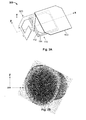
- Figs. 1a, 1b and 1c a perspective view and side view of an exemplary antenna system 100 according to the first embodiment of the invention, and a simulated radiating pattern are shown.
- the simulated radiating pattern in Fig. 1b illustrates the advantageous effect resulting from the parasitic element comprised in the antenna system 100.
- the antenna system 100 comprises a first planar antenna element 110.
- the embodiment is limited to antenna systems 100 where the first antenna element is a planar antenna element 110. Accordingly, the first antenna element is termed first planar antenna element 110.
- the first planar antenna element 110 is a corner truncated rectangular patch antenna. Thereby, the first planar antenna element 110 is capable of receiving/transmitting electromagnetic radio waves having a circular polarization.
- the first planar antenna element 110 is not restricted in this respect.
- the advantages to the antenna system 100 equally apply to configurations where the first planar antenna element 110 is capable of receiving/transmitting electromagnetic radio waves having a linear polarization.
- the first planar antenna element includes a patch electrode 112 (or patch element) which is provided (e.g. by means of printing or etching) on a dielectric substrate 114.
- the dielectric substrate 114 provides structural support to the patch electrode 112 of the first planar antenna element 110.
- the first planar antenna element 110 is not restricted in this respect.
- the advantages to the antenna system 100 equally apply to configurations where the first planar antenna element 110 includes a sheet electrode which is arranged at its predetermined position by, for example, a feed line which accordingly provides mechanical as well as electrical support to the sheet electrode of the first planar antenna element 110.
- the dielectric substrate 114 modifies the electrical size thereof.
- the dielectric substrate 114 has a relative permittivity ⁇ r which affects the wavelength of the electromagnetic radio waves received/transmitted by the patch electrode 112 at some frequency.
- an electrical size of the first planar antenna element 110 depends on the configuration thereof and may be different from the physical size of the structural elements to the first planar antenna element 110. Accordingly, further considerations with respect to an electromagnetic coupling of the first planar antenna element 110 and a planar parasitic element 130 mainly focus on the electrical size of both elements and not on their physical size.
- the term electrical size shall be understood as referring to the length of an electrical conductor of an antenna in terms of the wavelength of the electromagnetic radio waves emitted by that conductor.
- the electrical size of the electrical conductor is determined by, however, may vary from the fixed physical size thereof.
- an antenna gain is proportional to the electrical size of the antenna. At higher frequencies, more antenna gain can be obtained by increasing the electrical size of an antenna for a given physical antenna size. Accordingly, the first planar antenna element 110 including the patch electrode 112 provided on the dielectric substrate 114 advantageously results in an increase in antenna gain at high frequencies.
- same system additionally comprises at least one second antenna element 120.
- the antenna system 100 is shown with only a single second antenna element 120, the invention shall not be restricted in this respect.
- the principles of the antenna system 100 equally apply to configurations including a plurality of second antenna elements. Due to the combination of the first planar and the at least one second antenna element 110, 120 within the antenna system 100, the first planar and the at least one second antenna element 110, 120 interfere with each other, hence, resulting in adverse interference for the respective radiation patterns. Accordingly, in the absence of counter measures the radiating patterns of the first planar and the at least one second antenna element 110, 120 would suffer from deformation due to the electromagnetic coupling between the antenna elements in the antenna system 100.
- the at least one second antenna element 120 is a folded inverted-F antenna element. Accordingly, the at least one second antenna element 120 is particularly well suited for mobile communication, for instance, complying with long term evolution, LTE, specification for MIMO antennas as defined by 3GPP.
- the at least one second antenna element 120 is configured for lower frequencies than the first planar antenna element 110. Accordingly, the at least one second antenna element 120 has a large electrical size compared to the first planar antenna element 110. Due to this exemplary configuration the first planar antenna element 110 particularly suffers from deformation due to the electromagnetic coupling there between.
- the first planar antenna element 110 is adapted to a first frequency band; hence, is capable of transmitting/receiving electromagnetic radio waves at frequencies within the first frequency band.
- the at least one second antenna element 120 is adapted to a second frequency band; hence, is capable of transmitting/receiving electromagnetic radio waves at frequencies within the second frequency band.
- the first frequency band is higher or equal to the second frequency band.
- the electrical size of the at least one second antenna element 120 is larger than or equal to a resulting electrical size of the first planar element 110, hence, the electric shorter or equally sized first planar antenna element 110 is exposed to adverse interference by the at least one second antenna element 120, thereby resulting - in the absence of counter measures - in a deformed radiation pattern of the first planar antenna element 110.
- the first planar antenna element 110 and the at least one second antenna element 120 are arranged along a (i.e. single) axis (e.g. shown as x-axis in Fig. 1 a) . Accordingly, in the antenna system 100 the directivity of the radiating patterns of the first planar and the at least one second antenna element 110, 120, more particularly the azimuth angles ⁇ and the elevation angels ⁇ of the respective radiating patterns, have a predefined relationship to each other.
- the axis along which the first planar and the at least one second antenna element 110, 120 are arranged may correspond to a longitudinal (e.g. x-axis) or lateral axis (e.g. y-axis) of the antenna system 100.
- the arrangement of the first and the at least one second antenna element 110, 120 along an axis facilitates the antenna system 100 to be mounted on - for example - a vehicle rooftop in alignment with the longitudinal axis of the vehicle.
- the first planar and the at least one second antenna element 110, 120 are arranged within the near-field to each other.
- the at least one second antenna element 120 is arranged in the near-field of the first planar antenna element 110, e.g. applying the definition of near-field for the first planar antenna element 110.
- the term near-field has to be understood as the region around each of the first planar and at least one second antenna element 110, 120 where their radiating pattern is dominated by interference effects from the respective other of the first planar and at least one second antenna element 110, 120.
- the near-field is defined as the region with a radius r , where r ⁇ ⁇ .
- the antenna system 100 additionally comprises a planar parasitic element 130 which is arranged within the near-field of the first planar antenna element 110.
- the first planar antenna element 110 and the planar parasitic element 130 are arranged within the antenna system 100 such that the planar parasitic element 130 is electromagnetically coupled with the first planar antenna element 110.
- the planar parasitic element 130 acts as a director to the first planar antenna element 110.
- the term parasitic element (or parasitic radiator) has to be construed as a conductive element without electrically connection to a RF power source. Accordingly, the parasitic element is solely "driven” - and hence radiates - due to electromagnetic coupling with another antenna element which itself is connected to a feeding line.
- the planar parasitic element 130 is arranged substantially in parallel to the first planar antenna element 110. As shown for instance in Fig. 1c , the first planar antenna element 110 and the planar parasitic element 130 both extend substantially in parallel in a plane defined by the x-y axis. Thereby, a sufficiently strong electromagnetic coupling is realized between the first planar antenna element 110 and the planar parasitic element 130.
- a first plane defined by the extent of the first planar antenna element 110 and a second plane defined by the extent of the planar parasitic element 130 are substantially in parallel to each other. Tolerances to the parallel arrangement between the planar parasitic element 130 and the first planar antenna element 110 are in the region of 0 to 2° maximum angular deviation and may result from an inaccurate assembly of the two elements within the antenna system 100.
- the planar parasitic element 130 is a sheet electrode which is held in place by a housing of the antenna system 100.
- a housing of the antenna system 100 provides mechanical support to the planar parasitic element 130 such that it is arranged within the near-field of the first planar antenna element 110.
- the first planar antenna element 110 and the planar parasitic element 130 are arranged at a predetermined first distance d 1 to each other (cf. for instance Fig. 1c ).
- the planar parasitic element 130 is spaced at a predetermined first distance d 1 from the first planar antenna element 110, where the first distance allows for a sufficiently strong electromagnetic coupling between the planar parasitic element 130 and the first planar parasitic element 110.
- the first distance d 1 between the first planar antenna element 110 and the planar parasitic element 130, results in a (e.g. substantially) perpendicular arrangement of the first planar antenna element 110 and the planar parasitic element 130.
- the predetermined first distance d 1 between first planar antenna element 110 and the planar parasitic element 130 corresponds to separation along the vertical axis (e.g. z-axis in Fig. 1 c) of the antenna system 100.
- the size and the shape of the planar parasitic element 130 and the first distance d 1 thereof from the first planar antenna element 110 are determined in accordance with the first planar antenna element 110.
- the planar parasitic element 130 is configured to act as director to the first planar antenna element 110 due to an accordingly determined physical size, shape and first distance d 1 .
- planar parasitic element 130 for the planar parasitic element 130 to act as director to the first planar antenna element 110, planar parasitic element 130 has a by reduced electrical size compared to that of the first planar antenna element 110.
- This reduced electrical size is advantageous to compensate for a phase shift of transmitted electromagnetic radio wave due to the first distance d 1 . Accordingly, the amount of reduction of the electrical size of the first planar antenna element 110 depends on the first distance d 1 .
- the electric size of the various elements i.e. the first planar antenna element 110 and the planar parasitic element 130
- the electric size of the various elements differs from their respective physical size due to, for instance, the different dielectric substrates arranged at close proximity thereto.
- the planar parasitic element 130 has the same shape as the first planar antenna element 110.
- the planar parasitic element 130 is a corner-truncated sheet electrode.
- the first distance d 1 between the first planar antenna element 110 and the planar parasitic element 130 is between ⁇ /10 and ⁇ /4, where ⁇ corresponds to a wavelength of the first planar antenna element, particularly to a wavelength of a frequency of the first frequency band to which the first planar antenna element 110 is adapted.
- a first distance d 1 that is ⁇ /10 results in small phase shift of an induced current on the parasitic patch element 130 with respect to the first planar antenna element 110.
- the electrical size of the planar parasitic element 130 is only slightly reduced in comparison to that of the first planar antenna element 110.In other words, the electrical size of the parasitic patch element 130 is almost the same as the electrical size of the first planar antenna element 110.
- a first distance d 1 that is ⁇ /4 causes a larger phase shift of an induced current on the parasitic patch element 130 with respect to the first planar antenna element 110.
- the electrical size of the planar parasitic element 130 is substantially reduced in comparison to that of the first planar antenna element 110.
- the electrical size of the parasitic patch element 130 is decreased compared to that of the first planar antenna element 110 in order to compensate this effect.
- the latter configuration may be advantageous for antenna system with a limited amount of space.
- the center of the planar parasitic element 130 is offset with respect to the center of the first planar antenna element 110 in a second direction d 2 away from the at least one second antenna element 120, namely in a negative direction along the x-axis.
- the offset between the center of the planar parasitic element 130 and the center of first planar antenna element 110 is in a second direction d 2 that is opposite (i.e. in an opposite direction on the x-axis) with respect to the at least one second antenna element 120.
- the antenna system includes only a single second antenna element 120 - as is the case in the present embodiment - the second direction is opposite with respect to that single second antenna element 120; in case of a plurality of second antenna elements the second direction is opposite to one of the plurality of second antenna elements with which the first planar antenna element predominantly interferes. This case is discussed in more detail in connection with the third embodiment.
- same planar parasitic element 130 reduces a deformation of the radiating pattern of the first planar antenna element 110 in the antenna system 100.
- the deformation (e.g. deflection or displacement) of the radiating pattern of the first planar antenna element 110 is due to its interference with the at least one second antenna element 120.
- a simulated radiating pattern is that of the first planar antenna element 110.
- the simulated radiating pattern is shown in a top view with respect to the plane defined by the x- and y-axes of a coordinate system.
- the x-, y- and z-axes have a same orientation in all Figs. 1a, 1 b , and 1 c .
- the contour of the simulated radiating pattern of the first planar antenna element 110 is concentric with respect to the x-y plane and has only a minimum amount of deformation resulting from interference with the at least one second antenna element 120 in the antenna system 100.
- planar parasitic element 130 in the antenna system 100 in addition to the first planar and the at least one second antenna element 110, 120 allows for the beneficial effect that the interference in-between the individual antenna elements of the antenna system 100 is reduced thereby improving the respective radiation patterns.
- the antenna system 100 achieves this advantageous effect with the particular arrangement of the planar parasitic element 130 therein, namely without modifications to the first planar or to the at least one second antenna element 110, 120, and hence dispenses with the need for a more complicated design of the individual antenna elements.
- the advantageous design of the antenna system 100 becomes even more apparent when compared to a similar antenna system 200 shown in Figs. 2a and 2b which is similar to the antenna system 100, however does not include the planar parasitic element 130 thereof.
- FIGs. 2a and 2b a perspective view of an exemplary antenna system 200 useful for understanding the invention and a simulated radiating pattern thereof are shown.
- the antenna system 200 is based on the antenna system 100 of Fig. 1a where corresponding parts are given corresponding reference numerals and terms. The description of corresponding parts has been omitted for reasons of conciseness.
- the shown antenna system 200 differs, however, from the antenna system 100 in that it does not include a parasitic element 130 and hence suffers from interference between the first planar antenna element 110 and the at least one second antenna element 120 both also comprises in the antenna system 200.
- the simulated radiating pattern of the first planar antenna element 110 shown in Fig. 2b is deformed in a direction towards the at least one second antenna element 120.
- the contour of the simulated radiating pattern is not concentric with respect to the x-y plane. Instead the simulated radiating pattern of the first planar antenna element 110 is oriented in a positive direction along the x-axis as result of the interference with the at least one second antenna element 120.
- Figs. 3a and 3b a perspective view of an exemplary antenna system 300 according to the second embodiment of the invention, and a simulated radiating pattern thereof are shown.
- the simulated radiating pattern in Fig. 3b illustrates the advantageous effect resulting from the parasitic element comprised in the antenna system 300.
- the antenna system 300 is based on the antenna system 100 of Fig. 1a where corresponding parts are given corresponding reference numerals and terms. The description of corresponding parts has been omitted for reasons of conciseness.
- the shown antenna system 300 differs, however, from the antenna system 100 in that it includes at least one different second antenna element 320 in addition to the first planar antenna element 110 and the planar parasitic element 130.
- the antenna system 300 comprises a first planar antenna element 110, and at least one second planar antenna element 320, wherein the first planar antenna element 110 and the at least one second planar antenna element 320 are arranged along an axis, namely the x-axis. Further, the antenna system 300 comprises a planar parasitic element 130 arranged within the near-field of the first planar antenna element 110. The planar parasitic element 130 is arranged substantially in parallel to the first planar antenna element 110 and is arranged at a predetermined first distance d 1 therefrom.
- the center of the planar parasitic element 130 is offset with respect to the center of the first planar antenna element in a second direction d 2 away from the at least one second antenna element 120 along the axis, namely in a positive direction along the x-axis. Thereby, a deformation of the radiating pattern of the first planar antenna element 110 due to an interference with the at least one second antenna element 320 is reduced.
- the at least one different second antenna element 320 is a planar inverted-F antenna element. Accordingly, the at least one second antenna element 320 is particularly well suited for mobile communication, for instance, complying with long term evolution, LTE, specification for Main antennas as defined by 3GPP.
- planar parasitic element 130 in the antenna system 300 in addition to the first planar and the at least one second antenna element 110 and 320, allows for the beneficial effect that the interference in-between the individual antenna elements of the antenna system 300 is reduced thereby improving the respective radiation patterns.
- the antenna system 300 achieves this effect with the particular arrangement of the planar parasitic element 130 therein, namely without modifications to the first planar or to the at least one second antenna element 110, 320, and hence dispenses with the need for a more complicated design of the individual antenna elements.
- a simulated radiating pattern is that of the first planar antenna element 110.
- the simulated radiating pattern is shown in a top view with respect to the plane defined by the x- and y-axes of a coordinate system.
- the x-, y- and z-axes have a same orientation in all Figs. 3a, and 3b .
- Figs. 4a and 4b show an perspective view of the exemplary antenna system 400 useful for understanding the invention and a simulated radiating pattern thereof.
- the antenna system 400 is based on the antenna system 300 of Fig. 3a where corresponding parts are given corresponding reference numerals and terms. The description of corresponding parts has been omitted for reasons of conciseness.
- the simulated radiating pattern of the first planar antenna element 110 shown in Fig. 4b is deformed in a direction towards the at least one second antenna element 120, namely in a negative direction along the x-axis.
- the contour of the simulated radiating pattern is not concentric with respect to the x-y plane.
- Figs. 5a and 5b a perspective view of an exemplary antenna system 500 according to the third embodiment of the invention, and a simulated radiating pattern thereof are shown.
- the simulated radiating pattern in Fig. 5b illustrates the advantageous effect resulting from the parasitic element comprised in the antenna system 500.
- the antenna system 500 is based on the antenna systems 100 and 300 of Figs. 1a and 3a where corresponding parts are given corresponding reference numerals and terms. The description of corresponding parts has been omitted for reasons of conciseness.
- the shown antenna system 500 differs, however, from the antenna system 100 and 300 in that it includes plural second antenna elements 120, 320 in addition to the first planar antenna element 110 and the planar parasitic element 130.
- the antenna system 500 comprises a first planar antenna element 110, and plural second planar antenna elements 120, 320, wherein the first planar antenna element 110 and the plural second planar antenna elements 120, 320 are arranged along an axis, namely the x-axis in Fig. 5a , such that the first planar antenna element is arranged in-between two of the plurality of second antenna element 120, 320.
- the antenna system 500 comprises a planar parasitic element 130 arranged within the near-field of the first planar antenna element 110.
- the planar parasitic element 130 arranged substantially in parallel to the first planar antenna element 110 and is arranged at a predetermined first distance d 1 therefrom.
- the center of the planar parasitic element 130 is offset with respect to the center of the first planar antenna element 110 in a second direction d 2 away from a pre-dominantly interfering one of the plural second antenna elements 120, 320 along the axis, namely in a positive direction along the x-axis.
- a radiating pattern of the first planar antenna element 110 due to an interference with the at least one second antenna element 120 is reduced.
- That one of the plural second antenna elements 120, 320 interferes with the first planar antenna element 110 pre-dominantly which has a highest electromagnetic coupling to the first planar antenna element 110.
- a high electromagnetic coupling may result from, for instance, a similar size, shape or a smaller distance between the first planar antenna element 110 and the respective of the plural second antenna elements 120, 320.
- the two second antenna elements 120, 320, in-between which the first planar antenna element 110 is arranged have a different size, shape or are arranged at a different distance from the first planar antenna element 110 excludes the case that both of the second antenna elements 120, 320 equally interfere with the first planar antenna element 111 such that there is no predominant one.
- planar parasitic element 130 in the antenna system 500 in addition to the first planar and the plural second antenna elements 110, and 120, 320 allows for the beneficial effect that the interference in-between the individual antenna elements of the antenna system 500 is reduced thereby improving the respective radiation patterns.
- the antenna system 500 achieves this effect with the particular arrangement of the planar parasitic element 130 therein, namely without modifications to the first planar or to the plural second antenna elements 110, and 120, 320, and hence dispenses with the need for a more complicated design of the individual antenna elements.
- a simulated radiating pattern is that of the first planar antenna element 110.
- the simulated radiating pattern is shown in a top view with respect to the plane defined by the x- and y-axes of a coordinate system.
- the x-, y- and z-axes have a same orientation in all Figs. 5a, and 5b .
- Figs. 6a and 6b show an perspective view of the exemplary antenna system 600 useful for understanding the invention and a simulated radiating pattern thereof.
- the antenna system 600 is based on the antenna system 500 of Fig. 5a where corresponding parts are given corresponding reference numerals and terms. The description of corresponding parts has been omitted for reasons of conciseness.
- the simulated radiating pattern of the first planar antenna element 110 shown in Fig. 6b is deformed in a direction towards the at least one second antenna element 120, namely in a negative direction along the x-axis.
- the contour of the simulated radiating pattern is not concentric with respect to the x-y plane.
- each of the above discussed antenna systems of the various embodiments can be included in an antenna module for use on a vehicle rooftop.
- the antenna module preferably comprises, in addition to the antenna system, a housing for protecting the antenna system from outside influences, a base for arranging the antenna system thereon, an antenna matching circuit, and an electrically connection for transmitting/receiving electrical signals from the outside to/from the first antenna element and the second antenna elements of the antenna system.
- the vehicle rooftop provides for a ground plane to the first planar antenna element and the second antenna element of the antenna system.
Abstract
Description
- The invention relates to an improved antenna system comprising a first and a second antenna element and a parasitic element where the parasitic element allows for an improvement of the radiation pattern of at least one of the antenna elements. Further, the invention relates to an antenna module incorporating same antenna system.
- In the context of the invention, an antenna system is to be understood as an antenna arrangement comprising a first antenna element and a second antenna element.
- Generally, antenna systems are widely discussed in technology because the grouping of plural antenna elements in one system provides for various structural advantages. Particularly the assembly of an antenna system as a single structural module allows mechanical and electrical components to be shared between the plural antenna elements.
- Accordingly, in an antenna system the plural antenna elements may be arranged within and hence sharing a same housing, a same base, sharing same antenna circuitry, and a same electrically connection element (e.g. socket/plug) for transmitting/receiving electrical signals from the outside to/from the plural antenna elements within the antenna system, respectively.
- However, the arrangement of plural antenna elements in an antenna system suffers from disadvantages, particularly when the plural antenna elements are arranged in the near-field to each other. In this case, the plural antenna elements suffer from mutual interference effects particularly regarding their respective radiating patterns.
- In
WO 98/26471 A1 - In order to reduce interference effects, the antenna system additionally includes a frequency selective surface which is conductive to radio frequency energy in the first frequency range and reflective to radio frequency energy in the second frequency range. The frequency selective surface comprises preferably repetitive metallization pattern structures that display quasi band-pass or quasi band-reject filter characteristics to radio frequency signals impinging upon the frequency selective surface.
- Further,
US 6,917,340 B2 also relates to an antenna system comprising two antenna elements. In order to reduce the electromagnetic coupling and hence interference effects, one of the two antenna elements is subdivided into segments which have an electrical length corresponding to three/eight of the wavelength of the other antenna element. - Further, the segments of the one antenna element are electrically interconnected via electric reactance circuits which possess sufficiently high impedance in the frequency range of the other antenna element and sufficiently low impedance in the frequency range of the one antenna element.
- Even though the above described approaches allow for a reduced inference in the radiation pattern of two antenna elements, the design of the antenna system comprising the two antenna elements becomes more complicated in view of the incorporation of additional components, namely the manufacturing and arrangement of the incorporation of electric reactance circuits.
- In particular, the design of the electric reactance circuits and their arrangement on the respective antenna element is complex and necessitates additional development steps. Further the components of the electric reactance circuit as well as the, for instance soldered, electrical connection to the antenna elements introduces unacceptable variances to the frequency characteristic.
- In this respect it is an object of the invention to suggest an improved antenna system which overcomes the disadvantages noted above, e.g. a more complicated design of the individual antenna elements. Furthermore, it is another object of the invention to propose an antenna system which reduces interference in-between the individual antenna elements thereby improving the respective radiation patterns.
- According to a first aspect, an antenna system comprises a planar parasitic element in addition to a first planar and at least one second antenna element. The planar parasitic element allows for the beneficial effect that the interference in-between the first and the second antenna elements of the antenna system is reduced thereby improving the respective radiation patterns. According to an embodiment, an antenna system is proposed comprising a first planar antenna element, and at least one second antenna element, wherein the first planar antenna element and the at least one second antenna element are arranged along an axis. The antenna system further comprises a planar parasitic element arranged within the near-field of the first planar antenna element, the planar parasitic element being arranged substantially in parallel to the first planar antenna element and being arranged at a predetermined distance therefrom.
- The center of the planar parasitic element is offset with respect to the center of the first planar antenna element in a direction away from the at least one second antenna element along the axis, so as to reduce a deformation of the radiating pattern of the first planar antenna element due to an interference with the at least one second antenna element.
- According to another embodiment of the antenna system, each of the at least one second antenna element is arranged within the near-field of the first planar antenna element.
- According to a further embodiment of the antenna system, the first planar antenna element is capable of receiving/transmitting electromagnetic radio waves having a circular polarization.
- According to yet another embodiment of the antenna system, the first planar antenna element is a corner-truncated rectangular patch antenna element.
- According to an even further embodiment of the antenna system, the size and the shape of the planar parasitic element and the distance thereof from the first planar antenna element are determined in accordance with the first planar antenna element
- According to another embodiment of the antenna system, the planar parasitic element has no electrical connection to a RF power source.
- According to a further embodiment of the antenna system, the planar parasitic element has a reduced electrical size compared to that of the first planar antenna element determined in accordance with the distance thereof from the first planar antenna element.
- According to yet another embodiment of the antenna system, the planar parasitic element has the same shape as the first planar antenna element.
- According to an even further embodiment of the antenna system, the distance of the planar parasitic element from the first planar antenna element is between λ/10 and λ/4, where λ corresponds to a wavelength of the first planar antenna element.
- According to another embodiment of the antenna system, the first planar antenna element is adapted to a first frequency band, and the at least one second antenna element is adapted to a second frequency band, where the first frequency band is higher or equal to the second frequency band.
- According to a further embodiment of the antenna system, the first planar antenna element includes a patch electrode which is provided on a dielectric substrate.
- According to yet another embodiment of the antenna system, the planar parasitic element is a sheet electrode which is held in place by a housing of the antenna system.
- According to an even further embodiment of the antenna system, the at least one second antenna element is an inverted-F antenna element and/or a folded inverted-F antenna element.
- According to another embodiment of the antenna system, in case: a plurality of second antenna elements are comprised by the antenna system, and the first planar antenna element is arranged in-between two of the plurality of second antenna elements, and the two second antenna elements, in-between which the first planar antenna element is arranged, have different sizes, shapes compared to each other or are arranged at different distances from the first planar antenna element, the center of the planar parasitic element is offset with respect to the center of the first planar element in a direction away from that one of the plurality of second planar antenna elements which predominantly interferes with the first planar antenna element.
- According to a further embodiment of the antenna system, the center of first planar antenna element and bottom center of each of the at least one second antenna element are arranged on the axis.
- Further, a different embodiment an antenna module is proposed for use on a vehicle rooftop. The antenna module comprises an antenna system according to one of the previous embodiments, wherein the axis is aligned with the longitudinal axis of the vehicle, and the vehicle rooftop provides for a ground plane to the first planar antenna element and the at least one second antenna element.
- The accompanying drawings are incorporated into the specification and form a part of the specification to illustrate several embodiments of the present invention. These drawings, together with a description, serve to explain the principles of the invention.
- The drawings are merely for the purpose of illustrating the preferred and alternative examples of how the invention can be made and used, and are not to be construed as limiting the invention to only the illustrated and described embodiments.
- Furthermore, several aspects of the embodiments may form - individually or in different combinations - solutions according to the present invention. Further features and advantages will be become apparent from the following more particular description of the various embodiments of the invention as illustrated in the accompanying drawings, in which like references refer to like elements, and wherein:
- Figs. 1a, 1b and 1c
- illustrate a perspective view and side view of an exemplary antenna system according to the first embodiment of the invention, and a simulated radiating pattern thereof;
- Figs. 2a and 2b
- show a perspective view of an exemplary antenna system useful for understanding the first embodiment of the invention and a simulated radiating pattern thereof;
- Figs. 3a and 3b
- illustrate a perspective view of an exemplary antenna system according to the second embodiment of the invention, and a simulated radiating pattern thereof;
- Figs. 4a and 4b
- show a perspective view of an exemplary antenna system useful for understanding the second embodiment of the invention and a simulated radiating pattern thereof;
- Figs. 5a and 5b
- illustrate a perspective view of an exemplary antenna system according to the third embodiment of the invention, and a simulated radiating pattern thereof; and
- Figs. 6a and 6b
- show a perspective view of an exemplary antenna system useful for understanding the third embodiment of the invention and a simulated radiating pattern thereof.
- Referring now to
Figs. 1a, 1b and1c , a perspective view and side view of anexemplary antenna system 100 according to the first embodiment of the invention, and a simulated radiating pattern are shown. Particularly, the simulated radiating pattern inFig. 1b illustrates the advantageous effect resulting from the parasitic element comprised in theantenna system 100. - The
antenna system 100 comprises a firstplanar antenna element 110. Particularly, the embodiment is limited toantenna systems 100 where the first antenna element is aplanar antenna element 110. Accordingly, the first antenna element is termed firstplanar antenna element 110. - In an exemplary configuration of the
antenna system 100, the firstplanar antenna element 110 is a corner truncated rectangular patch antenna. Thereby, the firstplanar antenna element 110 is capable of receiving/transmitting electromagnetic radio waves having a circular polarization. However, the firstplanar antenna element 110 is not restricted in this respect. - Moreover, the advantages to the
antenna system 100 equally apply to configurations where the firstplanar antenna element 110 is capable of receiving/transmitting electromagnetic radio waves having a linear polarization. - In the exemplary configuration of the
antenna system 100, the first planar antenna element includes a patch electrode 112 (or patch element) which is provided (e.g. by means of printing or etching) on adielectric substrate 114. In this respect thedielectric substrate 114 provides structural support to thepatch electrode 112 of the firstplanar antenna element 110. However, the firstplanar antenna element 110 is not restricted in this respect. Moreover, the advantages to theantenna system 100 equally apply to configurations where the firstplanar antenna element 110 includes a sheet electrode which is arranged at its predetermined position by, for example, a feed line which accordingly provides mechanical as well as electrical support to the sheet electrode of the firstplanar antenna element 110. - Further to the other exemplary configuration of the
antenna system 100, thedielectric substrate 114, on which thepatch electrode 112 is provided to form the firstplanar antenna element 110, modifies the electrical size thereof. Thedielectric substrate 114 has a relative permittivity εr which affects the wavelength of the electromagnetic radio waves received/transmitted by thepatch electrode 112 at some frequency. - In more particular, the higher the relative permittivity εr of the
dielectric substrate 114 of the firstplanar antenna element 110, the smaller the electrical size of thepatch electrode 112 of the firstplanar antenna element 110. Accordingly, due to its provision on thedielectric substrate 114, thepatch electrode 112 of the firstplanar antenna element 110 has a reduced electrical size compared to its arrangement in air (i.e. without dielectric substrate). - Generally, an electrical size of the first
planar antenna element 110 depends on the configuration thereof and may be different from the physical size of the structural elements to the firstplanar antenna element 110. Accordingly, further considerations with respect to an electromagnetic coupling of the firstplanar antenna element 110 and a planarparasitic element 130 mainly focus on the electrical size of both elements and not on their physical size. - In the context of the invention, the term electrical size (or electrical length) shall be understood as referring to the length of an electrical conductor of an antenna in terms of the wavelength of the electromagnetic radio waves emitted by that conductor. In other words, the electrical size of the electrical conductor is determined by, however, may vary from the fixed physical size thereof.
- Advantageously, an antenna gain is proportional to the electrical size of the antenna. At higher frequencies, more antenna gain can be obtained by increasing the electrical size of an antenna for a given physical antenna size. Accordingly, the first
planar antenna element 110 including thepatch electrode 112 provided on thedielectric substrate 114 advantageously results in an increase in antenna gain at high frequencies. - Further to the
antenna system 100, same system additionally comprises at least onesecond antenna element 120. Even though theantenna system 100 is shown with only a singlesecond antenna element 120, the invention shall not be restricted in this respect. As will become apparent from, for instance, the third embodiment, the principles of theantenna system 100 equally apply to configurations including a plurality of second antenna elements. Due to the combination of the first planar and the at least onesecond antenna element antenna system 100, the first planar and the at least onesecond antenna element second antenna element antenna system 100. - Exemplarily, the at least one
second antenna element 120 is a folded inverted-F antenna element. Accordingly, the at least onesecond antenna element 120 is particularly well suited for mobile communication, for instance, complying with long term evolution, LTE, specification for MIMO antennas as defined by 3GPP. - In a further exemplary configuration of the
antenna system 100, the at least onesecond antenna element 120 is configured for lower frequencies than the firstplanar antenna element 110. Accordingly, the at least onesecond antenna element 120 has a large electrical size compared to the firstplanar antenna element 110. Due to this exemplary configuration the firstplanar antenna element 110 particularly suffers from deformation due to the electromagnetic coupling there between. - Further to this exemplary configuration, the first
planar antenna element 110 is adapted to a first frequency band; hence, is capable of transmitting/receiving electromagnetic radio waves at frequencies within the first frequency band. The at least onesecond antenna element 120 is adapted to a second frequency band; hence, is capable of transmitting/receiving electromagnetic radio waves at frequencies within the second frequency band. Particular to this exemplary configuration, the first frequency band is higher or equal to the second frequency band. - Due to this exemplary configuration of the first planar and the at least one
second antenna element second antenna element 120 is larger than or equal to a resulting electrical size of the firstplanar element 110, hence, the electric shorter or equally sized firstplanar antenna element 110 is exposed to adverse interference by the at least onesecond antenna element 120, thereby resulting - in the absence of counter measures - in a deformed radiation pattern of the firstplanar antenna element 110. - Further to the
antenna system 100, the firstplanar antenna element 110 and the at least onesecond antenna element 120 are arranged along a (i.e. single) axis (e.g. shown as x-axis inFig. 1 a) . Accordingly, in theantenna system 100 the directivity of the radiating patterns of the first planar and the at least onesecond antenna element - Particularly, the axis along which the first planar and the at least one
second antenna element antenna system 100. The arrangement of the first and the at least onesecond antenna element antenna system 100 to be mounted on - for example - a vehicle rooftop in alignment with the longitudinal axis of the vehicle. - In a further exemplary configuration of the
antenna system 100, the first planar and the at least onesecond antenna element second antenna element 120 is arranged in the near-field of the firstplanar antenna element 110, e.g. applying the definition of near-field for the firstplanar antenna element 110. - In the context of the invention, the term near-field has to be understood as the region around each of the first planar and at least one
second antenna element second antenna element second antenna element - Further, the
antenna system 100 additionally comprises a planarparasitic element 130 which is arranged within the near-field of the firstplanar antenna element 110. Particularly, the firstplanar antenna element 110 and the planarparasitic element 130 are arranged within theantenna system 100 such that the planarparasitic element 130 is electromagnetically coupled with the firstplanar antenna element 110. Moreover, the planarparasitic element 130 acts as a director to the firstplanar antenna element 110. - In the context of the invention, the term parasitic element (or parasitic radiator) has to be construed as a conductive element without electrically connection to a RF power source. Accordingly, the parasitic element is solely "driven" - and hence radiates - due to electromagnetic coupling with another antenna element which itself is connected to a feeding line.
- Further to the
antenna system 100, the planarparasitic element 130 is arranged substantially in parallel to the firstplanar antenna element 110. As shown for instance inFig. 1c , the firstplanar antenna element 110 and the planarparasitic element 130 both extend substantially in parallel in a plane defined by the x-y axis. Thereby, a sufficiently strong electromagnetic coupling is realized between the firstplanar antenna element 110 and the planarparasitic element 130. - In other words, a first plane defined by the extent of the first
planar antenna element 110 and a second plane defined by the extent of the planarparasitic element 130 are substantially in parallel to each other. Tolerances to the parallel arrangement between the planarparasitic element 130 and the firstplanar antenna element 110 are in the region of 0 to 2° maximum angular deviation and may result from an inaccurate assembly of the two elements within theantenna system 100. - In yet another exemplary configuration of the
antenna system 100, the planarparasitic element 130 is a sheet electrode which is held in place by a housing of theantenna system 100. In other words, a housing of theantenna system 100 provides mechanical support to the planarparasitic element 130 such that it is arranged within the near-field of the firstplanar antenna element 110. - The first
planar antenna element 110 and the planarparasitic element 130 are arranged at a predetermined first distance d 1 to each other (cf. for instanceFig. 1c ). In other words, the planarparasitic element 130 is spaced at a predetermined first distance d 1 from the firstplanar antenna element 110, where the first distance allows for a sufficiently strong electromagnetic coupling between the planarparasitic element 130 and the first planarparasitic element 110. - In more particular, the first distance d 1, between the first
planar antenna element 110 and the planarparasitic element 130, results in a (e.g. substantially) perpendicular arrangement of the firstplanar antenna element 110 and the planarparasitic element 130. For example, the predetermined first distance d 1 between firstplanar antenna element 110 and the planarparasitic element 130 corresponds to separation along the vertical axis (e.g. z-axis inFig. 1 c) of theantenna system 100. - In an even further exemplary configuration of the
antenna system 100, the size and the shape of the planarparasitic element 130 and the first distance d 1 thereof from the firstplanar antenna element 110 are determined in accordance with the firstplanar antenna element 110. Particularly, the planarparasitic element 130 is configured to act as director to the firstplanar antenna element 110 due to an accordingly determined physical size, shape and first distance d 1. - More particularly, for the planar
parasitic element 130 to act as director to the firstplanar antenna element 110, planarparasitic element 130 has a by reduced electrical size compared to that of the firstplanar antenna element 110. This reduced electrical size is advantageous to compensate for a phase shift of transmitted electromagnetic radio wave due to the first distance d 1. Accordingly, the amount of reduction of the electrical size of the firstplanar antenna element 110 depends on the first distance d 1. - Specifically, it shall be emphasized in this respect that the electric size of the various elements (i.e. the first
planar antenna element 110 and the planar parasitic element 130) differs from their respective physical size due to, for instance, the different dielectric substrates arranged at close proximity thereto. - Even further to this exemplary configuration of the
antenna system 100, the planarparasitic element 130 has the same shape as the firstplanar antenna element 110. Exemplarily, the planarparasitic element 130 is a corner-truncated sheet electrode. - In an exemplary configuration of the
antenna system 100, the first distance d 1 between the firstplanar antenna element 110 and the planarparasitic element 130 is between λ/10 and λ/4, where λ corresponds to a wavelength of the first planar antenna element, particularly to a wavelength of a frequency of the first frequency band to which the firstplanar antenna element 110 is adapted. - In particular, a first distance d 1 that is λ/10 results in small phase shift of an induced current on the
parasitic patch element 130 with respect to the firstplanar antenna element 110. In order to compensate for this small phase shift, the electrical size of the planarparasitic element 130 is only slightly reduced in comparison to that of the first planar antenna element 110.In other words, the electrical size of theparasitic patch element 130 is almost the same as the electrical size of the firstplanar antenna element 110. - Conversely, a first distance d 1 that is λ/4 causes a larger phase shift of an induced current on the
parasitic patch element 130 with respect to the firstplanar antenna element 110. In order to compensate for this larger phase shift, the electrical size of the planarparasitic element 130 is substantially reduced in comparison to that of the firstplanar antenna element 110. In other words, the electrical size of theparasitic patch element 130 is decreased compared to that of the firstplanar antenna element 110 in order to compensate this effect. The latter configuration may be advantageous for antenna system with a limited amount of space. - Further to the
antenna system 100, the center of the planarparasitic element 130 is offset with respect to the center of the firstplanar antenna element 110 in a second direction d 2 away from the at least onesecond antenna element 120, namely in a negative direction along the x-axis. In other words, the offset between the center of the planarparasitic element 130 and the center of firstplanar antenna element 110 is in a second direction d 2 that is opposite (i.e. in an opposite direction on the x-axis) with respect to the at least onesecond antenna element 120. - In more detail, in case the antenna system includes only a single second antenna element 120 - as is the case in the present embodiment - the second direction is opposite with respect to that single
second antenna element 120; in case of a plurality of second antenna elements the second direction is opposite to one of the plurality of second antenna elements with which the first planar antenna element predominantly interferes. This case is discussed in more detail in connection with the third embodiment. - Advantageously, due to the offset of center of the planar
parasitic element 130 with respect to the center of the firstplanar antenna element 110 in a direction d 2 away from the at least onesecond antenna element 120, same planarparasitic element 130 reduces a deformation of the radiating pattern of the firstplanar antenna element 110 in theantenna system 100. The deformation (e.g. deflection or displacement) of the radiating pattern of the firstplanar antenna element 110 is due to its interference with the at least onesecond antenna element 120. - Particularly, the advantageous effect of reducing a deformation of the radiating pattern in the
antenna system 100 is shown inFig. 1b , where a simulated radiating pattern is that of the firstplanar antenna element 110. The simulated radiating pattern is shown in a top view with respect to the plane defined by the x- and y-axes of a coordinate system. The x-, y- and z-axes have a same orientation in allFigs. 1a, 1 b , and1 c . - In this respect, it can be readily appreciated from
Fig. 1b that the contour of the simulated radiating pattern of the firstplanar antenna element 110 is concentric with respect to the x-y plane and has only a minimum amount of deformation resulting from interference with the at least onesecond antenna element 120 in theantenna system 100. - In summary, the particular arrangement of the planar
parasitic element 130 in theantenna system 100 in addition to the first planar and the at least onesecond antenna element antenna system 100 is reduced thereby improving the respective radiation patterns. - In addition, the
antenna system 100 achieves this advantageous effect with the particular arrangement of the planarparasitic element 130 therein, namely without modifications to the first planar or to the at least onesecond antenna element - The advantageous design of the
antenna system 100 becomes even more apparent when compared to asimilar antenna system 200 shown inFigs. 2a and 2b which is similar to theantenna system 100, however does not include the planarparasitic element 130 thereof. - Particularly, in
Figs. 2a and 2b a perspective view of anexemplary antenna system 200 useful for understanding the invention and a simulated radiating pattern thereof are shown. Theantenna system 200 is based on theantenna system 100 ofFig. 1a where corresponding parts are given corresponding reference numerals and terms. The description of corresponding parts has been omitted for reasons of conciseness. - The shown
antenna system 200 differs, however, from theantenna system 100 in that it does not include aparasitic element 130 and hence suffers from interference between the firstplanar antenna element 110 and the at least onesecond antenna element 120 both also comprises in theantenna system 200. - Due to the absence of the parasitic element in the
antenna system 200, the simulated radiating pattern of the firstplanar antenna element 110 shown inFig. 2b is deformed in a direction towards the at least onesecond antenna element 120. In other words, the contour of the simulated radiating pattern is not concentric with respect to the x-y plane. Instead the simulated radiating pattern of the firstplanar antenna element 110 is oriented in a positive direction along the x-axis as result of the interference with the at least onesecond antenna element 120. - Referring now to
Figs. 3a and 3b , a perspective view of anexemplary antenna system 300 according to the second embodiment of the invention, and a simulated radiating pattern thereof are shown. Particularly, the simulated radiating pattern inFig. 3b illustrates the advantageous effect resulting from the parasitic element comprised in theantenna system 300. Theantenna system 300 is based on theantenna system 100 ofFig. 1a where corresponding parts are given corresponding reference numerals and terms. The description of corresponding parts has been omitted for reasons of conciseness. - Moreover, the shown
antenna system 300 differs, however, from theantenna system 100 in that it includes at least one differentsecond antenna element 320 in addition to the firstplanar antenna element 110 and the planarparasitic element 130. - In more detail, the
antenna system 300 comprises a firstplanar antenna element 110, and at least one secondplanar antenna element 320, wherein the firstplanar antenna element 110 and the at least one secondplanar antenna element 320 are arranged along an axis, namely the x-axis. Further, theantenna system 300 comprises a planarparasitic element 130 arranged within the near-field of the firstplanar antenna element 110. The planarparasitic element 130 is arranged substantially in parallel to the firstplanar antenna element 110 and is arranged at a predetermined first distance d 1 therefrom. - Further, the center of the planar
parasitic element 130 is offset with respect to the center of the first planar antenna element in a second direction d 2 away from the at least onesecond antenna element 120 along the axis, namely in a positive direction along the x-axis. Thereby, a deformation of the radiating pattern of the firstplanar antenna element 110 due to an interference with the at least onesecond antenna element 320 is reduced. - The same considerations for the arrangement of the planar
parasitic element 130, discussed above with respect to theantenna system 100, also apply to theantenna system 200 thereby resulting in same exemplary configurations thereto. - Exemplarily, the at least one different
second antenna element 320 is a planar inverted-F antenna element. Accordingly, the at least onesecond antenna element 320 is particularly well suited for mobile communication, for instance, complying with long term evolution, LTE, specification for Main antennas as defined by 3GPP. - In summary, the particular arrangement of the planar
parasitic element 130 in theantenna system 300, in addition to the first planar and the at least onesecond antenna element antenna system 300 is reduced thereby improving the respective radiation patterns. - In addition, the
antenna system 300 achieves this effect with the particular arrangement of the planarparasitic element 130 therein, namely without modifications to the first planar or to the at least onesecond antenna element - Particularly, the advantageous effect of reducing a deformation of the radiating pattern in the
antenna system 300 is shown inFig. 3b , where a simulated radiating pattern is that of the firstplanar antenna element 110. The simulated radiating pattern is shown in a top view with respect to the plane defined by the x- and y-axes of a coordinate system. The x-, y- and z-axes have a same orientation in allFigs. 3a, and 3b . - The advantageous effects of the
antenna system 300 become even more apparent when compared to asimilar antenna system 400, whereFigs. 4a and 4b show an perspective view of theexemplary antenna system 400 useful for understanding the invention and a simulated radiating pattern thereof. Theantenna system 400 is based on theantenna system 300 ofFig. 3a where corresponding parts are given corresponding reference numerals and terms. The description of corresponding parts has been omitted for reasons of conciseness. - Due to the absence of the parasitic element in the
antenna system 400, the simulated radiating pattern of the firstplanar antenna element 110 shown inFig. 4b is deformed in a direction towards the at least onesecond antenna element 120, namely in a negative direction along the x-axis. In other words, the contour of the simulated radiating pattern is not concentric with respect to the x-y plane. - Referring now to
Figs. 5a and 5b , a perspective view of anexemplary antenna system 500 according to the third embodiment of the invention, and a simulated radiating pattern thereof are shown. Particularly, the simulated radiating pattern inFig. 5b illustrates the advantageous effect resulting from the parasitic element comprised in theantenna system 500. Theantenna system 500 is based on theantenna systems Figs. 1a and3a where corresponding parts are given corresponding reference numerals and terms. The description of corresponding parts has been omitted for reasons of conciseness. - Moreover, the shown
antenna system 500 differs, however, from theantenna system second antenna elements planar antenna element 110 and the planarparasitic element 130. - In more detail, the
antenna system 500 comprises a firstplanar antenna element 110, and plural secondplanar antenna elements planar antenna element 110 and the plural secondplanar antenna elements Fig. 5a , such that the first planar antenna element is arranged in-between two of the plurality ofsecond antenna element - Further, the
antenna system 500 comprises a planarparasitic element 130 arranged within the near-field of the firstplanar antenna element 110. The planarparasitic element 130 arranged substantially in parallel to the firstplanar antenna element 110 and is arranged at a predetermined first distance d 1 therefrom. - Further, the center of the planar
parasitic element 130 is offset with respect to the center of the firstplanar antenna element 110 in a second direction d 2 away from a pre-dominantly interfering one of the pluralsecond antenna elements planar antenna element 110 due to an interference with the at least onesecond antenna element 120 is reduced. - In an exemplary configuration of the
antenna system 500, that one of the pluralsecond antenna elements planar antenna element 110 pre-dominantly which has a highest electromagnetic coupling to the firstplanar antenna element 110. Such a high electromagnetic coupling may result from, for instance, a similar size, shape or a smaller distance between the firstplanar antenna element 110 and the respective of the pluralsecond antenna elements second antenna elements planar antenna element 110 is arranged, have a different size, shape or are arranged at a different distance from the firstplanar antenna element 110 excludes the case that both of thesecond antenna elements - The same considerations for the arrangement of the planar
parasitic element 130, discussed above with respect to theantenna system 100, also apply to theantenna system 500 thereby resulting in same exemplary configurations thereto. - In summary, the particular arrangement of the planar
parasitic element 130 in theantenna system 500 in addition to the first planar and the pluralsecond antenna elements antenna system 500 is reduced thereby improving the respective radiation patterns. - In addition, the
antenna system 500 achieves this effect with the particular arrangement of the planarparasitic element 130 therein, namely without modifications to the first planar or to the pluralsecond antenna elements - Particularly, the advantageous effect of reducing a deformation of the radiating pattern in the
antenna system 500 is shown inFig. 5b , where a simulated radiating pattern is that of the firstplanar antenna element 110. The simulated radiating pattern is shown in a top view with respect to the plane defined by the x- and y-axes of a coordinate system. The x-, y- and z-axes have a same orientation in allFigs. 5a, and 5b . - The advantageous effects of the
antenna system 500 become even more apparent when compared to asimilar antenna system 600, whereFigs. 6a and 6b show an perspective view of theexemplary antenna system 600 useful for understanding the invention and a simulated radiating pattern thereof. - The
antenna system 600 is based on theantenna system 500 ofFig. 5a where corresponding parts are given corresponding reference numerals and terms. The description of corresponding parts has been omitted for reasons of conciseness. - Due to the absence of the parasitic element in the
antenna system 600, the simulated radiating pattern of the firstplanar antenna element 110 shown inFig. 6b is deformed in a direction towards the at least onesecond antenna element 120, namely in a negative direction along the x-axis. In other words, the contour of the simulated radiating pattern is not concentric with respect to the x-y plane. - Finally, each of the above discussed antenna systems of the various embodiments can be included in an antenna module for use on a vehicle rooftop. For this purpose, the antenna module preferably comprises, in addition to the antenna system, a housing for protecting the antenna system from outside influences, a base for arranging the antenna system thereon, an antenna matching circuit, and an electrically connection for transmitting/receiving electrical signals from the outside to/from the first antenna element and the second antenna elements of the antenna system. Further, the vehicle rooftop provides for a ground plane to the first planar antenna element and the second antenna element of the antenna system.
-
Reference Numeral(s) Description 100, 200, 300, 400, 500, 600 Antenna system 110 First planar antenna element 112 Patch electrode 114 Dielectric substrate 120, 320 Second antenna element 130 Planar parasitic element
Claims (15)
- Antenna system, comprising:a first planar antenna element (110), andat least one second antenna element (120; 320),wherein the first planar antenna element and the at least one second antenna element are arranged along an axis,the antenna system further comprising:a planar parasitic element (130) arranged within the near-field of the first planar antenna element, the planar parasitic element being arranged substantially in parallel to the first planar antenna element and being arranged at a predetermined distance (d1) therefrom, andwherein the center of the planar parasitic element is offset with respect to the center of the first planar antenna element in a direction (d2) away from the at least one second antenna element along the axis, so as to reduce a deformation of the radiating pattern of the first planar antenna element due to an interference with the at least one second antenna element.
- The antenna system according to claim 1, wherein each of the at least one second antenna element is arranged within the near-field of the first planar antenna element.
- The antenna system according to claims 1 or 2, wherein the first planar antenna element is capable of receiving/transmitting electromagnetic radio waves having a circular polarization.
- The antenna system according to one of claims 1 - 3, wherein the first planar antenna element is a corner-truncated rectangular patch antenna element.
- The antenna system according to one of claims 1 - 4, wherein the size and the shape of the planar parasitic element and the distance thereof from the first planar antenna element are determined in accordance with the first planar antenna element; and/or wherein the planar parasitic element has no electrical connection to a RF power source.
- The antenna system according to one of claims 1 - 5, wherein the planar parasitic element has a reduced electrical size compared to that of the first planar antenna element which is determined in accordance with the distance thereof from the first planar antenna element.
- The antenna system according to one of claims 1 - 6, wherein the planar parasitic element has the same shape as the first planar antenna element.
- The antenna system according to one of claims 1 - 7, wherein the distance of the planar parasitic element from the first planar antenna element is between λ/10 and λ/4, where λ corresponds to a wavelength of the first planar antenna element.
- The antenna system according to one of claims 1 - 8, wherein the first planar antenna element is adapted to a first frequency band, and the at least one second antenna element is adapted to a second frequency band, and where the first frequency band is higher or equal to the second frequency band.
- The antenna system according to one of claims 1 - 9, wherein the first planar antenna element includes a patch electrode (112) which is provided on a dielectric substrate (114).
- The antenna system according to one of claims 1 - 10, wherein the planar parasitic element is a sheet electrode which is held in place by a housing of the antenna system.
- The antenna system according to one of claims 1 - 11, wherein the at least one second antenna element is a inverted-F antenna element and/or a folded inverted-F antenna element.
- The antenna system according to one of claims 1 - 12, wherein, in case:• a plurality of second antenna elements are comprised by the antenna system, and• the first planar antenna element is arranged in-between two of the plurality of second antenna elements, and• the two second antenna elements, in-between which the first planar antenna element is arranged, have different sizes, shapes compared to each other or are arranged at different distances from the first planar antenna element,the center of the planar parasitic element is offset with respect to the center of the first planar element in a direction away from that one of the plurality of second planar antenna elements which predominantly interferes with the first planar antenna element.
- The antenna system according to one of claims 1 - 13, wherein the center of first planar antenna element and bottom center of each of the at least one second antenna element are arranged on the axis.
- An antenna module for use on a vehicle rooftop, comprising:an antenna system according to one of claims 1 - 14, whereinthe axis is aligned with the longitudinal axis of the vehicle, andthe vehicle rooftop provides for a ground plane to the first planar antenna element and the at least one second antenna element.
Priority Applications (5)
| Application Number | Priority Date | Filing Date | Title |
|---|---|---|---|
| EP15166282.2A EP3091608B1 (en) | 2015-05-04 | 2015-05-04 | Antenna system and antenna module with a parasitic element for radiation pattern improvements |
| PCT/EP2016/060005 WO2016177782A1 (en) | 2015-05-04 | 2016-05-04 | Antenna system and antenna module with a parasitic element for radiation pattern improvements |
| CN201680026271.1A CN107567667A (en) | 2015-05-04 | 2016-05-04 | With the antenna system and Anneta module for the improved parasitic antenna of radiation pattern |
| JP2017556931A JP6522786B2 (en) | 2015-05-04 | 2016-05-04 | Antenna system and antenna module having a non-excitation element for improvement of radiation pattern |
| US15/801,906 US20180123236A1 (en) | 2015-05-04 | 2017-11-02 | Antenna System and Antenna Module With a Parasitic Element For Radiation Pattern Improvements |
Applications Claiming Priority (1)
| Application Number | Priority Date | Filing Date | Title |
|---|---|---|---|
| EP15166282.2A EP3091608B1 (en) | 2015-05-04 | 2015-05-04 | Antenna system and antenna module with a parasitic element for radiation pattern improvements |
Publications (2)
| Publication Number | Publication Date |
|---|---|
| EP3091608A1 true EP3091608A1 (en) | 2016-11-09 |
| EP3091608B1 EP3091608B1 (en) | 2021-08-04 |
Family
ID=53039786
Family Applications (1)
| Application Number | Title | Priority Date | Filing Date |
|---|---|---|---|
| EP15166282.2A Active EP3091608B1 (en) | 2015-05-04 | 2015-05-04 | Antenna system and antenna module with a parasitic element for radiation pattern improvements |
Country Status (5)
| Country | Link |
|---|---|
| US (1) | US20180123236A1 (en) |
| EP (1) | EP3091608B1 (en) |
| JP (1) | JP6522786B2 (en) |
| CN (1) | CN107567667A (en) |
| WO (1) | WO2016177782A1 (en) |
Cited By (2)
| Publication number | Priority date | Publication date | Assignee | Title |
|---|---|---|---|---|
| WO2022072105A1 (en) * | 2020-10-01 | 2022-04-07 | Google Llc | Collocated mmwave and sub-6 ghz antennas |
| US11450948B2 (en) * | 2016-12-06 | 2022-09-20 | Yokowo Co., Ltd. | Antenna device |
Families Citing this family (3)
| Publication number | Priority date | Publication date | Assignee | Title |
|---|---|---|---|---|
| CN110710057A (en) * | 2017-06-06 | 2020-01-17 | 株式会社村田制作所 | Antenna with a shield |
| US11444367B2 (en) * | 2020-08-11 | 2022-09-13 | GM Global Technology Operations LLC | Glass-mounted antenna package for a motor vehicle |
| US11848502B2 (en) | 2020-12-23 | 2023-12-19 | Getac Holdings Corporation | Electronic device |
Citations (6)
| Publication number | Priority date | Publication date | Assignee | Title |
|---|---|---|---|---|
| WO1998026471A2 (en) | 1996-11-26 | 1998-06-18 | Ball Aerospace & Technologies Corp. | Frequency selective antenna |
| US6917340B2 (en) | 2003-02-06 | 2005-07-12 | Fuba Automative Gmbh & Co. Kg | Combination antenna arrangement for several wireless communication services for vehicles |
| EP1650830A1 (en) * | 2004-10-21 | 2006-04-26 | Electronics and Telecommunications Research Institute | Circularly polarized patch antenna using metal patch and transceiving array antenna using the same |
| WO2010098529A1 (en) * | 2009-02-27 | 2010-09-02 | Ace Antenna Corp. | Mimo antenna having parasitic elements |
| EP2348576A1 (en) * | 2010-01-15 | 2011-07-27 | Delphi Technologies, Inc. | Antenna module |
| US20140242903A1 (en) * | 2013-02-27 | 2014-08-28 | Microsoft Corporation | Dual band antenna pair with high isolation |
Family Cites Families (12)
| Publication number | Priority date | Publication date | Assignee | Title |
|---|---|---|---|---|
| JPH0793532B2 (en) * | 1988-12-27 | 1995-10-09 | 原田工業株式会社 | Flat patch antenna |
| US5220335A (en) * | 1990-03-30 | 1993-06-15 | The United States Of America As Represented By The Administrator Of The National Aeronautics And Space Administration | Planar microstrip Yagi antenna array |
| US7079079B2 (en) * | 2004-06-30 | 2006-07-18 | Skycross, Inc. | Low profile compact multi-band meanderline loaded antenna |
| JP4798368B2 (en) * | 2006-09-04 | 2011-10-19 | ミツミ電機株式会社 | Compound antenna device |
| US7724201B2 (en) * | 2008-02-15 | 2010-05-25 | Sierra Wireless, Inc. | Compact diversity antenna system |
| JP4849280B2 (en) * | 2009-06-29 | 2012-01-11 | ミツミ電機株式会社 | Antenna device and shield cover used therefor |
| US9306276B2 (en) * | 2011-07-13 | 2016-04-05 | Qualcomm Incorporated | Wideband antenna system with multiple antennas and at least one parasitic element |
| JP5076019B1 (en) * | 2011-10-19 | 2012-11-21 | 株式会社東芝 | ANTENNA DEVICE AND ELECTRONIC DEVICE HAVING THE ANTENNA DEVICE |
| US9755311B2 (en) * | 2012-05-29 | 2017-09-05 | Samsung Electronics Co., Ltd. | Circularly polarized patch antennas, antenna arrays, and devices including such antennas and arrays |
| US9184503B2 (en) * | 2012-08-09 | 2015-11-10 | Topcon Positioning Systems, Inc. | Compact circular polarization antenna system with reduced cross-polarization component |
| KR20140030696A (en) * | 2012-09-03 | 2014-03-12 | 현대모비스 주식회사 | Integrated antenna for the vehicle |
| US10199732B2 (en) * | 2014-12-30 | 2019-02-05 | Advanced Micro Devices, Inc. | Circular polarized antennas including static element |
-
2015
- 2015-05-04 EP EP15166282.2A patent/EP3091608B1/en active Active
-
2016
- 2016-05-04 CN CN201680026271.1A patent/CN107567667A/en active Pending
- 2016-05-04 JP JP2017556931A patent/JP6522786B2/en not_active Expired - Fee Related
- 2016-05-04 WO PCT/EP2016/060005 patent/WO2016177782A1/en active Application Filing
-
2017
- 2017-11-02 US US15/801,906 patent/US20180123236A1/en not_active Abandoned
Patent Citations (6)
| Publication number | Priority date | Publication date | Assignee | Title |
|---|---|---|---|---|
| WO1998026471A2 (en) | 1996-11-26 | 1998-06-18 | Ball Aerospace & Technologies Corp. | Frequency selective antenna |
| US6917340B2 (en) | 2003-02-06 | 2005-07-12 | Fuba Automative Gmbh & Co. Kg | Combination antenna arrangement for several wireless communication services for vehicles |
| EP1650830A1 (en) * | 2004-10-21 | 2006-04-26 | Electronics and Telecommunications Research Institute | Circularly polarized patch antenna using metal patch and transceiving array antenna using the same |
| WO2010098529A1 (en) * | 2009-02-27 | 2010-09-02 | Ace Antenna Corp. | Mimo antenna having parasitic elements |
| EP2348576A1 (en) * | 2010-01-15 | 2011-07-27 | Delphi Technologies, Inc. | Antenna module |
| US20140242903A1 (en) * | 2013-02-27 | 2014-08-28 | Microsoft Corporation | Dual band antenna pair with high isolation |
Cited By (2)
| Publication number | Priority date | Publication date | Assignee | Title |
|---|---|---|---|---|
| US11450948B2 (en) * | 2016-12-06 | 2022-09-20 | Yokowo Co., Ltd. | Antenna device |
| WO2022072105A1 (en) * | 2020-10-01 | 2022-04-07 | Google Llc | Collocated mmwave and sub-6 ghz antennas |
Also Published As
| Publication number | Publication date |
|---|---|
| JP6522786B2 (en) | 2019-05-29 |
| CN107567667A (en) | 2018-01-09 |
| WO2016177782A1 (en) | 2016-11-10 |
| US20180123236A1 (en) | 2018-05-03 |
| EP3091608B1 (en) | 2021-08-04 |
| JP2018518884A (en) | 2018-07-12 |
Similar Documents
| Publication | Publication Date | Title |
|---|---|---|
| US9590304B2 (en) | Broadband antenna | |
| US20180123236A1 (en) | Antenna System and Antenna Module With a Parasitic Element For Radiation Pattern Improvements | |
| US8525741B2 (en) | Multi-loop antenna system and electronic apparatus having the same | |
| US8723751B2 (en) | Antenna system with planar dipole antennas and electronic apparatus having the same | |
| US8791865B2 (en) | Multi-loop antenna system and electronic apparatus having the same | |
| US20150061952A1 (en) | Broadband Antenna | |
| US9620863B2 (en) | Antenna device | |
| US8648762B2 (en) | Loop array antenna system and electronic apparatus having the same | |
| WO2008156429A1 (en) | Broadband antenna for wireless communications | |
| EP3698433A1 (en) | Cavity supported patch antenna | |
| JP2018530251A (en) | Communication device | |
| US20090231221A1 (en) | Dielectric rod antenna and method for operating the antenna | |
| US10431881B2 (en) | Electronic apparatus and dual band printed antenna of the same | |
| CN104466394A (en) | Broadband antenna | |
| US8159400B2 (en) | Chip antenna and mobile-communication terminal having the same | |
| US9660329B2 (en) | Directional antenna | |
| US20140327592A1 (en) | Antenna structure and wireless communication device employing same | |
| US9722311B2 (en) | Antenna device with continuous bending structure and application system using the same | |
| CN111276824A (en) | Antenna structure and wireless communication device with same | |
| CN111082221B (en) | Loop antenna | |
| CN210379412U (en) | Antenna, antenna assembly and electronic equipment | |
| US11158958B2 (en) | Dual band antenna | |
| KR101309505B1 (en) | Mimo antenna | |
| KR101482168B1 (en) | Antenna module using planar inverted-f antenna | |
| TWI509889B (en) | Plate-type antenna having a signal-isolating structure |
Legal Events
| Date | Code | Title | Description |
|---|---|---|---|
| PUAI | Public reference made under article 153(3) epc to a published international application that has entered the european phase |
Free format text: ORIGINAL CODE: 0009012 |
|
| AK | Designated contracting states |
Kind code of ref document: A1 Designated state(s): AL AT BE BG CH CY CZ DE DK EE ES FI FR GB GR HR HU IE IS IT LI LT LU LV MC MK MT NL NO PL PT RO RS SE SI SK SM TR |
|
| AX | Request for extension of the european patent |
Extension state: BA ME |
|
| STAA | Information on the status of an ep patent application or granted ep patent |
Free format text: STATUS: REQUEST FOR EXAMINATION WAS MADE |
|
| 17P | Request for examination filed |
Effective date: 20170509 |
|
| RBV | Designated contracting states (corrected) |
Designated state(s): AL AT BE BG CH CY CZ DE DK EE ES FI FR GB GR HR HU IE IS IT LI LT LU LV MC MK MT NL NO PL PT RO RS SE SI SK SM TR |
|
| STAA | Information on the status of an ep patent application or granted ep patent |
Free format text: STATUS: EXAMINATION IS IN PROGRESS |
|
| 17Q | First examination report despatched |
Effective date: 20200128 |
|
| STAA | Information on the status of an ep patent application or granted ep patent |
Free format text: STATUS: EXAMINATION IS IN PROGRESS |
|
| GRAP | Despatch of communication of intention to grant a patent |
Free format text: ORIGINAL CODE: EPIDOSNIGR1 |
|
| STAA | Information on the status of an ep patent application or granted ep patent |
Free format text: STATUS: GRANT OF PATENT IS INTENDED |
|
| INTG | Intention to grant announced |
Effective date: 20210401 |
|
| GRAS | Grant fee paid |
Free format text: ORIGINAL CODE: EPIDOSNIGR3 |
|
| GRAA | (expected) grant |
Free format text: ORIGINAL CODE: 0009210 |
|
| STAA | Information on the status of an ep patent application or granted ep patent |
Free format text: STATUS: THE PATENT HAS BEEN GRANTED |
|
| AK | Designated contracting states |
Kind code of ref document: B1 Designated state(s): AL AT BE BG CH CY CZ DE DK EE ES FI FR GB GR HR HU IE IS IT LI LT LU LV MC MK MT NL NO PL PT RO RS SE SI SK SM TR |
|
| REG | Reference to a national code |
Ref country code: GB Ref legal event code: FG4D |
|
| REG | Reference to a national code |
Ref country code: AT Ref legal event code: REF Ref document number: 1417941 Country of ref document: AT Kind code of ref document: T Effective date: 20210815 |
|
| REG | Reference to a national code |
Ref country code: CH Ref legal event code: EP |
|
| REG | Reference to a national code |
Ref country code: DE Ref legal event code: R096 Ref document number: 602015071866 Country of ref document: DE |
|
| REG | Reference to a national code |
Ref country code: IE Ref legal event code: FG4D |
|
| REG | Reference to a national code |
Ref country code: LT Ref legal event code: MG9D |
|
| REG | Reference to a national code |
Ref country code: NL Ref legal event code: MP Effective date: 20210804 |
|
| REG | Reference to a national code |
Ref country code: AT Ref legal event code: MK05 Ref document number: 1417941 Country of ref document: AT Kind code of ref document: T Effective date: 20210804 |
|
| PG25 | Lapsed in a contracting state [announced via postgrant information from national office to epo] |
Ref country code: RS Free format text: LAPSE BECAUSE OF FAILURE TO SUBMIT A TRANSLATION OF THE DESCRIPTION OR TO PAY THE FEE WITHIN THE PRESCRIBED TIME-LIMIT Effective date: 20210804 Ref country code: SE Free format text: LAPSE BECAUSE OF FAILURE TO SUBMIT A TRANSLATION OF THE DESCRIPTION OR TO PAY THE FEE WITHIN THE PRESCRIBED TIME-LIMIT Effective date: 20210804 Ref country code: HR Free format text: LAPSE BECAUSE OF FAILURE TO SUBMIT A TRANSLATION OF THE DESCRIPTION OR TO PAY THE FEE WITHIN THE PRESCRIBED TIME-LIMIT Effective date: 20210804 Ref country code: LT Free format text: LAPSE BECAUSE OF FAILURE TO SUBMIT A TRANSLATION OF THE DESCRIPTION OR TO PAY THE FEE WITHIN THE PRESCRIBED TIME-LIMIT Effective date: 20210804 Ref country code: AT Free format text: LAPSE BECAUSE OF FAILURE TO SUBMIT A TRANSLATION OF THE DESCRIPTION OR TO PAY THE FEE WITHIN THE PRESCRIBED TIME-LIMIT Effective date: 20210804 Ref country code: BG Free format text: LAPSE BECAUSE OF FAILURE TO SUBMIT A TRANSLATION OF THE DESCRIPTION OR TO PAY THE FEE WITHIN THE PRESCRIBED TIME-LIMIT Effective date: 20211104 Ref country code: FI Free format text: LAPSE BECAUSE OF FAILURE TO SUBMIT A TRANSLATION OF THE DESCRIPTION OR TO PAY THE FEE WITHIN THE PRESCRIBED TIME-LIMIT Effective date: 20210804 Ref country code: ES Free format text: LAPSE BECAUSE OF FAILURE TO SUBMIT A TRANSLATION OF THE DESCRIPTION OR TO PAY THE FEE WITHIN THE PRESCRIBED TIME-LIMIT Effective date: 20210804 Ref country code: PT Free format text: LAPSE BECAUSE OF FAILURE TO SUBMIT A TRANSLATION OF THE DESCRIPTION OR TO PAY THE FEE WITHIN THE PRESCRIBED TIME-LIMIT Effective date: 20211206 Ref country code: NO Free format text: LAPSE BECAUSE OF FAILURE TO SUBMIT A TRANSLATION OF THE DESCRIPTION OR TO PAY THE FEE WITHIN THE PRESCRIBED TIME-LIMIT Effective date: 20211104 |
|
| PG25 | Lapsed in a contracting state [announced via postgrant information from national office to epo] |
Ref country code: PL Free format text: LAPSE BECAUSE OF FAILURE TO SUBMIT A TRANSLATION OF THE DESCRIPTION OR TO PAY THE FEE WITHIN THE PRESCRIBED TIME-LIMIT Effective date: 20210804 Ref country code: LV Free format text: LAPSE BECAUSE OF FAILURE TO SUBMIT A TRANSLATION OF THE DESCRIPTION OR TO PAY THE FEE WITHIN THE PRESCRIBED TIME-LIMIT Effective date: 20210804 Ref country code: GR Free format text: LAPSE BECAUSE OF FAILURE TO SUBMIT A TRANSLATION OF THE DESCRIPTION OR TO PAY THE FEE WITHIN THE PRESCRIBED TIME-LIMIT Effective date: 20211105 |
|
| PG25 | Lapsed in a contracting state [announced via postgrant information from national office to epo] |
Ref country code: NL Free format text: LAPSE BECAUSE OF FAILURE TO SUBMIT A TRANSLATION OF THE DESCRIPTION OR TO PAY THE FEE WITHIN THE PRESCRIBED TIME-LIMIT Effective date: 20210804 |
|
| PG25 | Lapsed in a contracting state [announced via postgrant information from national office to epo] |
Ref country code: DK Free format text: LAPSE BECAUSE OF FAILURE TO SUBMIT A TRANSLATION OF THE DESCRIPTION OR TO PAY THE FEE WITHIN THE PRESCRIBED TIME-LIMIT Effective date: 20210804 |
|
| REG | Reference to a national code |
Ref country code: DE Ref legal event code: R097 Ref document number: 602015071866 Country of ref document: DE |
|
| PG25 | Lapsed in a contracting state [announced via postgrant information from national office to epo] |
Ref country code: SM Free format text: LAPSE BECAUSE OF FAILURE TO SUBMIT A TRANSLATION OF THE DESCRIPTION OR TO PAY THE FEE WITHIN THE PRESCRIBED TIME-LIMIT Effective date: 20210804 Ref country code: SK Free format text: LAPSE BECAUSE OF FAILURE TO SUBMIT A TRANSLATION OF THE DESCRIPTION OR TO PAY THE FEE WITHIN THE PRESCRIBED TIME-LIMIT Effective date: 20210804 Ref country code: RO Free format text: LAPSE BECAUSE OF FAILURE TO SUBMIT A TRANSLATION OF THE DESCRIPTION OR TO PAY THE FEE WITHIN THE PRESCRIBED TIME-LIMIT Effective date: 20210804 Ref country code: EE Free format text: LAPSE BECAUSE OF FAILURE TO SUBMIT A TRANSLATION OF THE DESCRIPTION OR TO PAY THE FEE WITHIN THE PRESCRIBED TIME-LIMIT Effective date: 20210804 Ref country code: CZ Free format text: LAPSE BECAUSE OF FAILURE TO SUBMIT A TRANSLATION OF THE DESCRIPTION OR TO PAY THE FEE WITHIN THE PRESCRIBED TIME-LIMIT Effective date: 20210804 Ref country code: AL Free format text: LAPSE BECAUSE OF FAILURE TO SUBMIT A TRANSLATION OF THE DESCRIPTION OR TO PAY THE FEE WITHIN THE PRESCRIBED TIME-LIMIT Effective date: 20210804 |
|
| PLBE | No opposition filed within time limit |
Free format text: ORIGINAL CODE: 0009261 |
|
| STAA | Information on the status of an ep patent application or granted ep patent |
Free format text: STATUS: NO OPPOSITION FILED WITHIN TIME LIMIT |
|
| 26N | No opposition filed |
Effective date: 20220506 |
|
| PG25 | Lapsed in a contracting state [announced via postgrant information from national office to epo] |
Ref country code: IT Free format text: LAPSE BECAUSE OF FAILURE TO SUBMIT A TRANSLATION OF THE DESCRIPTION OR TO PAY THE FEE WITHIN THE PRESCRIBED TIME-LIMIT Effective date: 20210804 |
|
| PG25 | Lapsed in a contracting state [announced via postgrant information from national office to epo] |
Ref country code: SI Free format text: LAPSE BECAUSE OF FAILURE TO SUBMIT A TRANSLATION OF THE DESCRIPTION OR TO PAY THE FEE WITHIN THE PRESCRIBED TIME-LIMIT Effective date: 20210804 |
|
| REG | Reference to a national code |
Ref country code: CH Ref legal event code: PL |
|
| REG | Reference to a national code |
Ref country code: BE Ref legal event code: MM Effective date: 20220531 |
|
| GBPC | Gb: european patent ceased through non-payment of renewal fee |
Effective date: 20220504 |
|
| PG25 | Lapsed in a contracting state [announced via postgrant information from national office to epo] |
Ref country code: MC Free format text: LAPSE BECAUSE OF FAILURE TO SUBMIT A TRANSLATION OF THE DESCRIPTION OR TO PAY THE FEE WITHIN THE PRESCRIBED TIME-LIMIT Effective date: 20210804 Ref country code: LU Free format text: LAPSE BECAUSE OF NON-PAYMENT OF DUE FEES Effective date: 20220504 Ref country code: LI Free format text: LAPSE BECAUSE OF NON-PAYMENT OF DUE FEES Effective date: 20220531 Ref country code: CH Free format text: LAPSE BECAUSE OF NON-PAYMENT OF DUE FEES Effective date: 20220531 |
|
| PG25 | Lapsed in a contracting state [announced via postgrant information from national office to epo] |
Ref country code: IE Free format text: LAPSE BECAUSE OF NON-PAYMENT OF DUE FEES Effective date: 20220504 Ref country code: FR Free format text: LAPSE BECAUSE OF NON-PAYMENT OF DUE FEES Effective date: 20220531 |
|
| PG25 | Lapsed in a contracting state [announced via postgrant information from national office to epo] |
Ref country code: GB Free format text: LAPSE BECAUSE OF NON-PAYMENT OF DUE FEES Effective date: 20220504 Ref country code: BE Free format text: LAPSE BECAUSE OF NON-PAYMENT OF DUE FEES Effective date: 20220531 |
|
| PGFP | Annual fee paid to national office [announced via postgrant information from national office to epo] |
Ref country code: DE Payment date: 20230307 Year of fee payment: 9 |
|
| PG25 | Lapsed in a contracting state [announced via postgrant information from national office to epo] |
Ref country code: HU Free format text: LAPSE BECAUSE OF FAILURE TO SUBMIT A TRANSLATION OF THE DESCRIPTION OR TO PAY THE FEE WITHIN THE PRESCRIBED TIME-LIMIT; INVALID AB INITIO Effective date: 20150504 |