EP3091573A2 - Semiconductor chip package assembly with improved heat dissipation performance - Google Patents
Semiconductor chip package assembly with improved heat dissipation performance Download PDFInfo
- Publication number
- EP3091573A2 EP3091573A2 EP16161852.5A EP16161852A EP3091573A2 EP 3091573 A2 EP3091573 A2 EP 3091573A2 EP 16161852 A EP16161852 A EP 16161852A EP 3091573 A2 EP3091573 A2 EP 3091573A2
- Authority
- EP
- European Patent Office
- Prior art keywords
- chip package
- semiconductor chip
- solder
- pad
- dummy pad
- Prior art date
- Legal status (The legal status is an assumption and is not a legal conclusion. Google has not performed a legal analysis and makes no representation as to the accuracy of the status listed.)
- Ceased
Links
Images



Classifications
-
- H—ELECTRICITY
- H10—SEMICONDUCTOR DEVICES; ELECTRIC SOLID-STATE DEVICES NOT OTHERWISE PROVIDED FOR
- H10W—GENERIC PACKAGES, INTERCONNECTIONS, CONNECTORS OR OTHER CONSTRUCTIONAL DETAILS OF DEVICES COVERED BY CLASS H10
- H10W40/00—Arrangements for thermal protection or thermal control
- H10W40/20—Arrangements for cooling
- H10W40/22—Arrangements for cooling characterised by their shape, e.g. having conical or cylindrical projections
-
- H—ELECTRICITY
- H10—SEMICONDUCTOR DEVICES; ELECTRIC SOLID-STATE DEVICES NOT OTHERWISE PROVIDED FOR
- H10W—GENERIC PACKAGES, INTERCONNECTIONS, CONNECTORS OR OTHER CONSTRUCTIONAL DETAILS OF DEVICES COVERED BY CLASS H10
- H10W72/00—Interconnections or connectors in packages
- H10W72/20—Bump connectors, e.g. solder bumps or copper pillars; Dummy bumps; Thermal bumps
-
- H—ELECTRICITY
- H10—SEMICONDUCTOR DEVICES; ELECTRIC SOLID-STATE DEVICES NOT OTHERWISE PROVIDED FOR
- H10W—GENERIC PACKAGES, INTERCONNECTIONS, CONNECTORS OR OTHER CONSTRUCTIONAL DETAILS OF DEVICES COVERED BY CLASS H10
- H10W40/00—Arrangements for thermal protection or thermal control
- H10W40/20—Arrangements for cooling
- H10W40/22—Arrangements for cooling characterised by their shape, e.g. having conical or cylindrical projections
- H10W40/226—Arrangements for cooling characterised by their shape, e.g. having conical or cylindrical projections characterised by projecting parts, e.g. fins to increase surface area
- H10W40/228—Arrangements for cooling characterised by their shape, e.g. having conical or cylindrical projections characterised by projecting parts, e.g. fins to increase surface area the projecting parts being wire-shaped or pin-shaped
-
- H—ELECTRICITY
- H10—SEMICONDUCTOR DEVICES; ELECTRIC SOLID-STATE DEVICES NOT OTHERWISE PROVIDED FOR
- H10W—GENERIC PACKAGES, INTERCONNECTIONS, CONNECTORS OR OTHER CONSTRUCTIONAL DETAILS OF DEVICES COVERED BY CLASS H10
- H10W70/00—Package substrates; Interposers; Redistribution layers [RDL]
- H10W70/01—Manufacture or treatment
- H10W70/05—Manufacture or treatment of insulating or insulated package substrates, or of interposers, or of redistribution layers
- H10W70/08—Manufacture or treatment of insulating or insulated package substrates, or of interposers, or of redistribution layers by depositing layers on the chip or wafer, e.g. "chip-first" RDLs
- H10W70/09—Manufacture or treatment of insulating or insulated package substrates, or of interposers, or of redistribution layers by depositing layers on the chip or wafer, e.g. "chip-first" RDLs extending onto an encapsulation that laterally surrounds the chip or wafer, e.g. fan-out wafer level package [FOWLP] RDLs
-
- H—ELECTRICITY
- H10—SEMICONDUCTOR DEVICES; ELECTRIC SOLID-STATE DEVICES NOT OTHERWISE PROVIDED FOR
- H10W—GENERIC PACKAGES, INTERCONNECTIONS, CONNECTORS OR OTHER CONSTRUCTIONAL DETAILS OF DEVICES COVERED BY CLASS H10
- H10W70/00—Package substrates; Interposers; Redistribution layers [RDL]
- H10W70/60—Insulating or insulated package substrates; Interposers; Redistribution layers
- H10W70/611—Insulating or insulated package substrates; Interposers; Redistribution layers for connecting multiple chips together
- H10W70/614—Insulating or insulated package substrates; Interposers; Redistribution layers for connecting multiple chips together the multiple chips being integrally enclosed
-
- H—ELECTRICITY
- H10—SEMICONDUCTOR DEVICES; ELECTRIC SOLID-STATE DEVICES NOT OTHERWISE PROVIDED FOR
- H10W—GENERIC PACKAGES, INTERCONNECTIONS, CONNECTORS OR OTHER CONSTRUCTIONAL DETAILS OF DEVICES COVERED BY CLASS H10
- H10W70/00—Package substrates; Interposers; Redistribution layers [RDL]
- H10W70/60—Insulating or insulated package substrates; Interposers; Redistribution layers
- H10W70/62—Insulating or insulated package substrates; Interposers; Redistribution layers characterised by their interconnections
- H10W70/65—Shapes or dispositions of interconnections
-
- H—ELECTRICITY
- H10—SEMICONDUCTOR DEVICES; ELECTRIC SOLID-STATE DEVICES NOT OTHERWISE PROVIDED FOR
- H10W—GENERIC PACKAGES, INTERCONNECTIONS, CONNECTORS OR OTHER CONSTRUCTIONAL DETAILS OF DEVICES COVERED BY CLASS H10
- H10W70/00—Package substrates; Interposers; Redistribution layers [RDL]
- H10W70/60—Insulating or insulated package substrates; Interposers; Redistribution layers
- H10W70/67—Insulating or insulated package substrates; Interposers; Redistribution layers characterised by their insulating layers or insulating parts
- H10W70/69—Insulating materials thereof
-
- H—ELECTRICITY
- H10—SEMICONDUCTOR DEVICES; ELECTRIC SOLID-STATE DEVICES NOT OTHERWISE PROVIDED FOR
- H10W—GENERIC PACKAGES, INTERCONNECTIONS, CONNECTORS OR OTHER CONSTRUCTIONAL DETAILS OF DEVICES COVERED BY CLASS H10
- H10W72/00—Interconnections or connectors in packages
-
- H—ELECTRICITY
- H10—SEMICONDUCTOR DEVICES; ELECTRIC SOLID-STATE DEVICES NOT OTHERWISE PROVIDED FOR
- H10W—GENERIC PACKAGES, INTERCONNECTIONS, CONNECTORS OR OTHER CONSTRUCTIONAL DETAILS OF DEVICES COVERED BY CLASS H10
- H10W72/00—Interconnections or connectors in packages
- H10W72/90—Bond pads, in general
-
- H—ELECTRICITY
- H10—SEMICONDUCTOR DEVICES; ELECTRIC SOLID-STATE DEVICES NOT OTHERWISE PROVIDED FOR
- H10W—GENERIC PACKAGES, INTERCONNECTIONS, CONNECTORS OR OTHER CONSTRUCTIONAL DETAILS OF DEVICES COVERED BY CLASS H10
- H10W74/00—Encapsulations, e.g. protective coatings
- H10W74/10—Encapsulations, e.g. protective coatings characterised by their shape or disposition
- H10W74/111—Encapsulations, e.g. protective coatings characterised by their shape or disposition the semiconductor body being completely enclosed
- H10W74/114—Encapsulations, e.g. protective coatings characterised by their shape or disposition the semiconductor body being completely enclosed by a substrate and the encapsulations
-
- H—ELECTRICITY
- H10—SEMICONDUCTOR DEVICES; ELECTRIC SOLID-STATE DEVICES NOT OTHERWISE PROVIDED FOR
- H10W—GENERIC PACKAGES, INTERCONNECTIONS, CONNECTORS OR OTHER CONSTRUCTIONAL DETAILS OF DEVICES COVERED BY CLASS H10
- H10W74/00—Encapsulations, e.g. protective coatings
- H10W74/10—Encapsulations, e.g. protective coatings characterised by their shape or disposition
- H10W74/111—Encapsulations, e.g. protective coatings characterised by their shape or disposition the semiconductor body being completely enclosed
- H10W74/129—Encapsulations, e.g. protective coatings characterised by their shape or disposition the semiconductor body being completely enclosed forming a chip-scale package [CSP]
-
- H—ELECTRICITY
- H10—SEMICONDUCTOR DEVICES; ELECTRIC SOLID-STATE DEVICES NOT OTHERWISE PROVIDED FOR
- H10W—GENERIC PACKAGES, INTERCONNECTIONS, CONNECTORS OR OTHER CONSTRUCTIONAL DETAILS OF DEVICES COVERED BY CLASS H10
- H10W90/00—Package configurations
-
- H—ELECTRICITY
- H10—SEMICONDUCTOR DEVICES; ELECTRIC SOLID-STATE DEVICES NOT OTHERWISE PROVIDED FOR
- H10W—GENERIC PACKAGES, INTERCONNECTIONS, CONNECTORS OR OTHER CONSTRUCTIONAL DETAILS OF DEVICES COVERED BY CLASS H10
- H10W90/00—Package configurations
- H10W90/701—Package configurations characterised by the relative positions of pads or connectors relative to package parts
-
- H—ELECTRICITY
- H10—SEMICONDUCTOR DEVICES; ELECTRIC SOLID-STATE DEVICES NOT OTHERWISE PROVIDED FOR
- H10W—GENERIC PACKAGES, INTERCONNECTIONS, CONNECTORS OR OTHER CONSTRUCTIONAL DETAILS OF DEVICES COVERED BY CLASS H10
- H10W70/00—Package substrates; Interposers; Redistribution layers [RDL]
- H10W70/60—Insulating or insulated package substrates; Interposers; Redistribution layers
-
- H—ELECTRICITY
- H10—SEMICONDUCTOR DEVICES; ELECTRIC SOLID-STATE DEVICES NOT OTHERWISE PROVIDED FOR
- H10W—GENERIC PACKAGES, INTERCONNECTIONS, CONNECTORS OR OTHER CONSTRUCTIONAL DETAILS OF DEVICES COVERED BY CLASS H10
- H10W70/00—Package substrates; Interposers; Redistribution layers [RDL]
- H10W70/60—Insulating or insulated package substrates; Interposers; Redistribution layers
- H10W70/67—Insulating or insulated package substrates; Interposers; Redistribution layers characterised by their insulating layers or insulating parts
- H10W70/68—Shapes or dispositions thereof
- H10W70/685—Shapes or dispositions thereof comprising multiple insulating layers
-
- H—ELECTRICITY
- H10—SEMICONDUCTOR DEVICES; ELECTRIC SOLID-STATE DEVICES NOT OTHERWISE PROVIDED FOR
- H10W—GENERIC PACKAGES, INTERCONNECTIONS, CONNECTORS OR OTHER CONSTRUCTIONAL DETAILS OF DEVICES COVERED BY CLASS H10
- H10W72/00—Interconnections or connectors in packages
- H10W72/071—Connecting or disconnecting
- H10W72/072—Connecting or disconnecting of bump connectors
-
- H—ELECTRICITY
- H10—SEMICONDUCTOR DEVICES; ELECTRIC SOLID-STATE DEVICES NOT OTHERWISE PROVIDED FOR
- H10W—GENERIC PACKAGES, INTERCONNECTIONS, CONNECTORS OR OTHER CONSTRUCTIONAL DETAILS OF DEVICES COVERED BY CLASS H10
- H10W72/00—Interconnections or connectors in packages
- H10W72/071—Connecting or disconnecting
- H10W72/072—Connecting or disconnecting of bump connectors
- H10W72/07251—Connecting or disconnecting of bump connectors characterised by changes in properties of the bump connectors during connecting
- H10W72/07253—Connecting or disconnecting of bump connectors characterised by changes in properties of the bump connectors during connecting changes in shapes
-
- H—ELECTRICITY
- H10—SEMICONDUCTOR DEVICES; ELECTRIC SOLID-STATE DEVICES NOT OTHERWISE PROVIDED FOR
- H10W—GENERIC PACKAGES, INTERCONNECTIONS, CONNECTORS OR OTHER CONSTRUCTIONAL DETAILS OF DEVICES COVERED BY CLASS H10
- H10W72/00—Interconnections or connectors in packages
- H10W72/071—Connecting or disconnecting
- H10W72/072—Connecting or disconnecting of bump connectors
- H10W72/07251—Connecting or disconnecting of bump connectors characterised by changes in properties of the bump connectors during connecting
- H10W72/07254—Connecting or disconnecting of bump connectors characterised by changes in properties of the bump connectors during connecting changes in dispositions
-
- H—ELECTRICITY
- H10—SEMICONDUCTOR DEVICES; ELECTRIC SOLID-STATE DEVICES NOT OTHERWISE PROVIDED FOR
- H10W—GENERIC PACKAGES, INTERCONNECTIONS, CONNECTORS OR OTHER CONSTRUCTIONAL DETAILS OF DEVICES COVERED BY CLASS H10
- H10W72/00—Interconnections or connectors in packages
- H10W72/071—Connecting or disconnecting
- H10W72/073—Connecting or disconnecting of die-attach connectors
-
- H—ELECTRICITY
- H10—SEMICONDUCTOR DEVICES; ELECTRIC SOLID-STATE DEVICES NOT OTHERWISE PROVIDED FOR
- H10W—GENERIC PACKAGES, INTERCONNECTIONS, CONNECTORS OR OTHER CONSTRUCTIONAL DETAILS OF DEVICES COVERED BY CLASS H10
- H10W72/00—Interconnections or connectors in packages
- H10W72/20—Bump connectors, e.g. solder bumps or copper pillars; Dummy bumps; Thermal bumps
- H10W72/231—Shapes
- H10W72/232—Plan-view shape, i.e. in top view
-
- H—ELECTRICITY
- H10—SEMICONDUCTOR DEVICES; ELECTRIC SOLID-STATE DEVICES NOT OTHERWISE PROVIDED FOR
- H10W—GENERIC PACKAGES, INTERCONNECTIONS, CONNECTORS OR OTHER CONSTRUCTIONAL DETAILS OF DEVICES COVERED BY CLASS H10
- H10W72/00—Interconnections or connectors in packages
- H10W72/20—Bump connectors, e.g. solder bumps or copper pillars; Dummy bumps; Thermal bumps
- H10W72/231—Shapes
- H10W72/234—Cross-sectional shape, i.e. in side view
-
- H—ELECTRICITY
- H10—SEMICONDUCTOR DEVICES; ELECTRIC SOLID-STATE DEVICES NOT OTHERWISE PROVIDED FOR
- H10W—GENERIC PACKAGES, INTERCONNECTIONS, CONNECTORS OR OTHER CONSTRUCTIONAL DETAILS OF DEVICES COVERED BY CLASS H10
- H10W72/00—Interconnections or connectors in packages
- H10W72/20—Bump connectors, e.g. solder bumps or copper pillars; Dummy bumps; Thermal bumps
- H10W72/231—Shapes
- H10W72/237—Multiple bump connectors having different shapes
-
- H—ELECTRICITY
- H10—SEMICONDUCTOR DEVICES; ELECTRIC SOLID-STATE DEVICES NOT OTHERWISE PROVIDED FOR
- H10W—GENERIC PACKAGES, INTERCONNECTIONS, CONNECTORS OR OTHER CONSTRUCTIONAL DETAILS OF DEVICES COVERED BY CLASS H10
- H10W72/00—Interconnections or connectors in packages
- H10W72/20—Bump connectors, e.g. solder bumps or copper pillars; Dummy bumps; Thermal bumps
- H10W72/241—Dispositions, e.g. layouts
-
- H—ELECTRICITY
- H10—SEMICONDUCTOR DEVICES; ELECTRIC SOLID-STATE DEVICES NOT OTHERWISE PROVIDED FOR
- H10W—GENERIC PACKAGES, INTERCONNECTIONS, CONNECTORS OR OTHER CONSTRUCTIONAL DETAILS OF DEVICES COVERED BY CLASS H10
- H10W72/00—Interconnections or connectors in packages
- H10W72/20—Bump connectors, e.g. solder bumps or copper pillars; Dummy bumps; Thermal bumps
- H10W72/241—Dispositions, e.g. layouts
- H10W72/244—Dispositions, e.g. layouts relative to underlying supporting features, e.g. bond pads, RDLs or vias
-
- H—ELECTRICITY
- H10—SEMICONDUCTOR DEVICES; ELECTRIC SOLID-STATE DEVICES NOT OTHERWISE PROVIDED FOR
- H10W—GENERIC PACKAGES, INTERCONNECTIONS, CONNECTORS OR OTHER CONSTRUCTIONAL DETAILS OF DEVICES COVERED BY CLASS H10
- H10W72/00—Interconnections or connectors in packages
- H10W72/20—Bump connectors, e.g. solder bumps or copper pillars; Dummy bumps; Thermal bumps
- H10W72/241—Dispositions, e.g. layouts
- H10W72/247—Dispositions of multiple bumps
-
- H—ELECTRICITY
- H10—SEMICONDUCTOR DEVICES; ELECTRIC SOLID-STATE DEVICES NOT OTHERWISE PROVIDED FOR
- H10W—GENERIC PACKAGES, INTERCONNECTIONS, CONNECTORS OR OTHER CONSTRUCTIONAL DETAILS OF DEVICES COVERED BY CLASS H10
- H10W72/00—Interconnections or connectors in packages
- H10W72/20—Bump connectors, e.g. solder bumps or copper pillars; Dummy bumps; Thermal bumps
- H10W72/251—Materials
- H10W72/252—Materials comprising solid metals or solid metalloids, e.g. PbSn, Ag or Cu
-
- H—ELECTRICITY
- H10—SEMICONDUCTOR DEVICES; ELECTRIC SOLID-STATE DEVICES NOT OTHERWISE PROVIDED FOR
- H10W—GENERIC PACKAGES, INTERCONNECTIONS, CONNECTORS OR OTHER CONSTRUCTIONAL DETAILS OF DEVICES COVERED BY CLASS H10
- H10W72/00—Interconnections or connectors in packages
- H10W72/20—Bump connectors, e.g. solder bumps or copper pillars; Dummy bumps; Thermal bumps
- H10W72/281—Auxiliary members
- H10W72/287—Flow barriers
-
- H—ELECTRICITY
- H10—SEMICONDUCTOR DEVICES; ELECTRIC SOLID-STATE DEVICES NOT OTHERWISE PROVIDED FOR
- H10W—GENERIC PACKAGES, INTERCONNECTIONS, CONNECTORS OR OTHER CONSTRUCTIONAL DETAILS OF DEVICES COVERED BY CLASS H10
- H10W72/00—Interconnections or connectors in packages
- H10W72/20—Bump connectors, e.g. solder bumps or copper pillars; Dummy bumps; Thermal bumps
- H10W72/29—Bond pads specially adapted therefor
-
- H—ELECTRICITY
- H10—SEMICONDUCTOR DEVICES; ELECTRIC SOLID-STATE DEVICES NOT OTHERWISE PROVIDED FOR
- H10W—GENERIC PACKAGES, INTERCONNECTIONS, CONNECTORS OR OTHER CONSTRUCTIONAL DETAILS OF DEVICES COVERED BY CLASS H10
- H10W72/00—Interconnections or connectors in packages
- H10W72/851—Dispositions of multiple connectors or interconnections
- H10W72/874—On different surfaces
-
- H—ELECTRICITY
- H10—SEMICONDUCTOR DEVICES; ELECTRIC SOLID-STATE DEVICES NOT OTHERWISE PROVIDED FOR
- H10W—GENERIC PACKAGES, INTERCONNECTIONS, CONNECTORS OR OTHER CONSTRUCTIONAL DETAILS OF DEVICES COVERED BY CLASS H10
- H10W72/00—Interconnections or connectors in packages
- H10W72/851—Dispositions of multiple connectors or interconnections
- H10W72/874—On different surfaces
- H10W72/884—Die-attach connectors and bond wires
-
- H—ELECTRICITY
- H10—SEMICONDUCTOR DEVICES; ELECTRIC SOLID-STATE DEVICES NOT OTHERWISE PROVIDED FOR
- H10W—GENERIC PACKAGES, INTERCONNECTIONS, CONNECTORS OR OTHER CONSTRUCTIONAL DETAILS OF DEVICES COVERED BY CLASS H10
- H10W72/00—Interconnections or connectors in packages
- H10W72/90—Bond pads, in general
- H10W72/941—Dispositions of bond pads
- H10W72/9413—Dispositions of bond pads on encapsulations
-
- H—ELECTRICITY
- H10—SEMICONDUCTOR DEVICES; ELECTRIC SOLID-STATE DEVICES NOT OTHERWISE PROVIDED FOR
- H10W—GENERIC PACKAGES, INTERCONNECTIONS, CONNECTORS OR OTHER CONSTRUCTIONAL DETAILS OF DEVICES COVERED BY CLASS H10
- H10W72/00—Interconnections or connectors in packages
- H10W72/90—Bond pads, in general
- H10W72/941—Dispositions of bond pads
- H10W72/9415—Dispositions of bond pads relative to the surface, e.g. recessed, protruding
-
- H—ELECTRICITY
- H10—SEMICONDUCTOR DEVICES; ELECTRIC SOLID-STATE DEVICES NOT OTHERWISE PROVIDED FOR
- H10W—GENERIC PACKAGES, INTERCONNECTIONS, CONNECTORS OR OTHER CONSTRUCTIONAL DETAILS OF DEVICES COVERED BY CLASS H10
- H10W74/00—Encapsulations, e.g. protective coatings
- H10W74/10—Encapsulations, e.g. protective coatings characterised by their shape or disposition
- H10W74/15—Encapsulations, e.g. protective coatings characterised by their shape or disposition on active surfaces of flip-chip devices, e.g. underfills
-
- H—ELECTRICITY
- H10—SEMICONDUCTOR DEVICES; ELECTRIC SOLID-STATE DEVICES NOT OTHERWISE PROVIDED FOR
- H10W—GENERIC PACKAGES, INTERCONNECTIONS, CONNECTORS OR OTHER CONSTRUCTIONAL DETAILS OF DEVICES COVERED BY CLASS H10
- H10W90/00—Package configurations
- H10W90/20—Configurations of stacked chips
-
- H—ELECTRICITY
- H10—SEMICONDUCTOR DEVICES; ELECTRIC SOLID-STATE DEVICES NOT OTHERWISE PROVIDED FOR
- H10W—GENERIC PACKAGES, INTERCONNECTIONS, CONNECTORS OR OTHER CONSTRUCTIONAL DETAILS OF DEVICES COVERED BY CLASS H10
- H10W90/00—Package configurations
- H10W90/20—Configurations of stacked chips
- H10W90/288—Configurations of stacked chips characterised by arrangements for thermal management of the stacked chips
-
- H—ELECTRICITY
- H10—SEMICONDUCTOR DEVICES; ELECTRIC SOLID-STATE DEVICES NOT OTHERWISE PROVIDED FOR
- H10W—GENERIC PACKAGES, INTERCONNECTIONS, CONNECTORS OR OTHER CONSTRUCTIONAL DETAILS OF DEVICES COVERED BY CLASS H10
- H10W90/00—Package configurations
- H10W90/701—Package configurations characterised by the relative positions of pads or connectors relative to package parts
- H10W90/721—Package configurations characterised by the relative positions of pads or connectors relative to package parts of bump connectors
-
- H—ELECTRICITY
- H10—SEMICONDUCTOR DEVICES; ELECTRIC SOLID-STATE DEVICES NOT OTHERWISE PROVIDED FOR
- H10W—GENERIC PACKAGES, INTERCONNECTIONS, CONNECTORS OR OTHER CONSTRUCTIONAL DETAILS OF DEVICES COVERED BY CLASS H10
- H10W90/00—Package configurations
- H10W90/701—Package configurations characterised by the relative positions of pads or connectors relative to package parts
- H10W90/721—Package configurations characterised by the relative positions of pads or connectors relative to package parts of bump connectors
- H10W90/722—Package configurations characterised by the relative positions of pads or connectors relative to package parts of bump connectors between stacked chips
-
- H—ELECTRICITY
- H10—SEMICONDUCTOR DEVICES; ELECTRIC SOLID-STATE DEVICES NOT OTHERWISE PROVIDED FOR
- H10W—GENERIC PACKAGES, INTERCONNECTIONS, CONNECTORS OR OTHER CONSTRUCTIONAL DETAILS OF DEVICES COVERED BY CLASS H10
- H10W90/00—Package configurations
- H10W90/701—Package configurations characterised by the relative positions of pads or connectors relative to package parts
- H10W90/721—Package configurations characterised by the relative positions of pads or connectors relative to package parts of bump connectors
- H10W90/724—Package configurations characterised by the relative positions of pads or connectors relative to package parts of bump connectors between a chip and a stacked insulating package substrate, interposer or RDL
-
- H—ELECTRICITY
- H10—SEMICONDUCTOR DEVICES; ELECTRIC SOLID-STATE DEVICES NOT OTHERWISE PROVIDED FOR
- H10W—GENERIC PACKAGES, INTERCONNECTIONS, CONNECTORS OR OTHER CONSTRUCTIONAL DETAILS OF DEVICES COVERED BY CLASS H10
- H10W90/00—Package configurations
- H10W90/701—Package configurations characterised by the relative positions of pads or connectors relative to package parts
- H10W90/721—Package configurations characterised by the relative positions of pads or connectors relative to package parts of bump connectors
- H10W90/728—Package configurations characterised by the relative positions of pads or connectors relative to package parts of bump connectors between a chip and a stacked discrete passive device, e.g. resistors, capacitors or inductors
-
- H—ELECTRICITY
- H10—SEMICONDUCTOR DEVICES; ELECTRIC SOLID-STATE DEVICES NOT OTHERWISE PROVIDED FOR
- H10W—GENERIC PACKAGES, INTERCONNECTIONS, CONNECTORS OR OTHER CONSTRUCTIONAL DETAILS OF DEVICES COVERED BY CLASS H10
- H10W90/00—Package configurations
- H10W90/701—Package configurations characterised by the relative positions of pads or connectors relative to package parts
- H10W90/731—Package configurations characterised by the relative positions of pads or connectors relative to package parts of die-attach connectors
- H10W90/734—Package configurations characterised by the relative positions of pads or connectors relative to package parts of die-attach connectors between a chip and a stacked insulating package substrate, interposer or RDL
-
- H—ELECTRICITY
- H10—SEMICONDUCTOR DEVICES; ELECTRIC SOLID-STATE DEVICES NOT OTHERWISE PROVIDED FOR
- H10W—GENERIC PACKAGES, INTERCONNECTIONS, CONNECTORS OR OTHER CONSTRUCTIONAL DETAILS OF DEVICES COVERED BY CLASS H10
- H10W90/00—Package configurations
- H10W90/701—Package configurations characterised by the relative positions of pads or connectors relative to package parts
- H10W90/751—Package configurations characterised by the relative positions of pads or connectors relative to package parts of bond wires
- H10W90/754—Package configurations characterised by the relative positions of pads or connectors relative to package parts of bond wires between a chip and a stacked insulating package substrate, interposer or RDL
Definitions
- the present invention relates to a semiconductor chip package assembly with improved heat dissipation performance.
- a chip (or a chip package) is electrically connected to a package substrate and mechanically bonded in a solder joining operation.
- the chip is aligned with and placed onto a placement site on the package substrate such that the solder balls are aligned with electrical pads or pre-solder on the substrate.
- the substrate is typically composed of an organic material or laminate. Heat is then applied causing the solder balls to alloy and form electrical connections between the chip and the package substrate.
- chip packages electrical performance and dissipation control are two major challenges.
- chip packages In the aspect of electrical performance, chip packages have to maintain signal integrity and operating frequency of semiconductor devices.
- dissipation control it is required that chip packages efficiently dissipate heat generated by the semiconductor chip.
- a heat spreader or lid typically composed of a high thermal conductivity material, and having substantially the same dimensions as the package substrate is typically attached over the substrate and the chip by a thermally conductive adhesive.
- the purpose of the heat spreader is to disperse the heat generated during operation to reduce stress in the package.
- the present invention aims at providing a semiconductor chip package assembly with improved heat dissipation performance.
- the semiconductor chip package assembly includes a package substrate having a chip mounting surface; a plurality of solder pads disposed on the chip mounting surface; a first dummy pad and a second dummy pad spaced apart from the first dummy pad disposed on the chip mounting surface; a solder mask on the chip mounting surface and partially covering the solder pads, the first dummy pad, and the second dummy pad; a chip package mounted on the chip mounting surface and electrically connected to the package substrate through a plurality of solder balls on respective solder pads; a discrete device having a first terminal and a second terminal disposed between the chip package and the package substrate; a first solder connecting the first terminal with the first dummy pad and the chip package; and a second solder connecting the second terminal with the second dummy pad and the chip package.
- the discrete device may comprise a land side capacitor, a de-coupling capacitor, a resistor, or an inductor.
- a semiconductor chip package assembly includes a substrate having a chip mounting surface; a plurality of solder pads disposed on the chip mounting surface; a first dummy pad and a second dummy pad spaced apart from the first dummy pad disposed on the chip mounting surface; a solder mask on the chip mounting surface and partially covering the solder pads, the first dummy pad, and the second dummy pad; a multi-chip package mounted on the chip mounting surface and electrically connected to the substrate through a plurality of solder balls on respective solder pads; a discrete device having a first terminal and a second terminal disposed between the chip package and the substrate; a first solder connecting the first terminal with the first dummy pad and the multi-chip package; and a second solder connecting the second terminal with the second dummy pad and the multi-chip package.
- a semiconductor chip package assembly includes a substrate having a chip mounting surface; a plurality of solder pads disposed on the chip mounting surface; a first dummy pad and a second dummy pad spaced apart from the first dummy pad disposed on the chip mounting surface; a solder mask on the chip mounting surface and partially covering the solder pads, the first dummy pad, and the second dummy pad; a package-on-package (PoP) mounted on the chip mounting surface and electrically connected to the substrate through a plurality of solder balls on respective solder pads; a discrete device having a first terminal and a second terminal disposed between the chip package and the substrate; a first solder connecting the first terminal with the first dummy pad and the PoP; and a second solder connecting the second terminal with the second dummy pad and the PoP.
- PoP package-on-package
- FIG. 1 is a schematic, cross-sectional diagram showing an exemplary semiconductor chip package assembly in accordance with one embodiment of the invention.
- the semiconductor chip package assembly 1 may comprise a chip package 100 directly mounted on chip mounting surface 200a of a package substrate 200 through an array of solder balls 250.
- the chip package 100 may comprise a semiconductor chip 10 that is encapsulated and surrounded by a molding compound 12.
- the active surface 10a having a plurality of input/output (I/O) pads 102 distributed thereon is not covered by the molding compound 12 and faces downwardly toward the package substrate 200.
- the inactive surface 10b of the semiconductor chip 10 may be covered with the molding compound 12, but is not limited thereto.
- the surrounding molding compound 12 may have a surface that is substantially flush with the active surface 10a.
- a redistribution layer (RDL) structure 20 may be formed on the active surface 10a and on the surrounding molding compound 12 to fan out the I/O pads 102.
- the RDL structure 20 may comprise at least one dielectric layer 120, at least one metal layer 110, and redistributed pads 112 on the land side of the chip package 100.
- solder balls 250 placed on the solder pads 212 of the package substrate 200 establish electrical connection between the chip package 100 and the package substrate 200.
- Such configuration is also known as a fan-out wafer level package (FOWLP).
- FOWLP fan-out wafer level package
- the structure of the chip package 100 shown in FIG. 1 is for illustration purposes only.
- the chip package 100 may be replaced with an unpackaged silicon chip or die.
- the chip package 100 may be replaced with a multi-die chip package such as Fan-out WLP (FO WLP) or other types of chip package.
- FO WLP Fan-out WLP
- epoxy or resin underfill may be applied between the solder balls 250.
- the solder balls 250 may be replaced with copper pillars or the like.
- the package substrate 200 may be replaced with a printed circuit board (PCB).
- semiconductor chip package assembly 1 further comprises at least one discrete device 150 mounted on the land side of the chip package 100.
- the discrete device 150 may include, but not limited to, a land side capacitor, a de-coupling capacitor, a resistor, or an inductor.
- the discrete device 150 such as a land side capacitor has two terminals 151 and 152, which are electrically coupled to V SS and V DD voltages, respectively, through the RDL structure 20.
- the two terminals 151 and 152 may be connected to the respective pads 111 in the RDL structure 20 by using solder 154.
- the two terminals 151 and 152 of the discrete device 150 are also connected to the respective pads 211 on the package substrate 200 through solder 154.
- the pads 211 are for heat dissipation and may be dummy pads.
- the dummy pads 211 may be electrically isolated from other metal traces on the package substrate 200, but is not limited thereto.
- the dummy pads 211 and the solder pads 212 may be partially covered with a solder mask 202.
- the solder mask 202 may cover a peripheral region of each of the pads 211 and 212 and may expose a central region of each of the pads 211 and 212.
- the heat generated by the chip package 100 can be efficiently dissipated through the solder 154, the discrete device 150, to the package substrate 200.
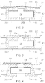
- FIG. 2 to FIG. 4 show different configuration of the land side capacitor and the heat dissipating pads 211 on the package substrate 200.
- RDL structure 20 the upper portion of the package substrate 200, and the discrete device 150
- the pads 111 of the RDL structure 20 of the chip package 100 are aligned with the dummy pads 211 on the package substrate 200.
- a recess or a slot 202a may be provided in the solder mask 202 between the two solder pads 211. If an underfill (not shown) is applied, the slot 202a may be filled with the underfill.
- the pads 111 of the RDL structure 20 of the chip package 100 are aligned with the dummy pads 211 on the package substrate 200.
- a recess or a slot 110a may be provided in the dielectric layer 110 between the pads 111. If an underfill (not shown) is applied, the slot 110a may be filled with the underfill.
- the pads 111 of the RDL structure 20 of the chip package 100 are misaligned with the dummy pads 211 on the package substrate 200. By increasing the distance between the two dummy pads 211, the overflow of the solder 154 may be avoided.
- FIG. 5 illustrates another embodiment of the invention, wherein like numeral numbers designate like regions, layers or elements.
- a semiconductor chip package assembly 1a is provided.
- the semiconductor chip package assembly 1a may comprise a multi-chip package 100a having at least two semiconductor chips 30 and 40 arranged on an RDL structure 20 in a side-by-side manner.
- the semiconductor chips 30 and 40 comprise a plurality of I/O pads 302 and 402 on their active surfaces, respectively.
- the RDL structure 20 may be formed on the active surfaces of the semiconductor chips 30 and 40, and on the molding compound 12 to fan out the I/O pads 302 and 402.
- the RDL structure 20 may comprise at least one dielectric layer 120, at least one metal layer 110, and redistributed pads 112 on the land side of the multi-chip package 100a.
- the semiconductor chip package assembly 1a further comprises at least one discrete device 150 mounted on the land side of the multi-chip package 100a.
- the discrete device 150 may include, but not limited to, a land side capacitor, a de-coupling capacitor, a resistor, or an inductor.
- the discrete device 150 such as a land side capacitor has two terminals 151 and 152, which may be electrically coupled to Vss and V DD voltages, respectively, through the RDL structure 20.
- the two terminals 151 and 152 may be connected to the respective pads 111 in the RDL structure 20 by using solder 154.
- the two terminals 151 and 152 of the discrete device 150 are also connected to the respective pads 211 on the package substrate 200 through solder 154.
- the pads 211 are for heat dissipation and may be dummy pads.
- the dummy pads 211 may be electrically isolated from other metal traces on the package substrate 200, but is not limited thereto.
- the dummy pads 211 and the solder pads 212 may be partially covered with a solder mask 202.
- the solder mask 202 may cover a peripheral region of each of the pads 211 and 212 and may expose a central region of each of the pads 211 and 212.
- the heat generated by the multi-chip package 100a can be efficiently dissipated through the solder 154, the discrete device 150, to the package substrate 200.
- FIG. 6 illustrates yet another embodiment of the invention, wherein like numeral numbers designate like regions, layers or elements.
- a semiconductor chip package assembly 1b is provided.
- the semiconductor chip package assembly 1b may comprise a lower chip package 100b having at least one semiconductor chip 50 disposed on a lower RDL structure 20a.
- the semiconductor chip 50 comprises a plurality of I/O pads 502 on its active surface.
- the lower RDL structure 20a may be formed on the active surface and on the surrounding molding compound 12 to fan out the I/O pads 502.
- the lower RDL structure 20a may comprise at least one dielectric layer 120, at least one metal layer 110, and redistributed pads 112 on the land side of the chip package 100.
- An upper chip package 100c is stacked on the lower chip package 100b to constitute a package-on-package (PoP) 500.
- the upper chip package 100c may comprise at least one semiconductor chip 60 encapsulated by a molding compound 13.
- the semiconductor chip 60 may be a memory chip such as a DRAM chip, but is not limited thereto.
- the upper chip package 100c may be electrically coupled to the lower chip package 100b through a plurality of solder balls 350 and a plurality of through mold vias (TMVs) 420.
- TSVs through mold vias
- an upper RDL structure 20b may be provided between the upper chip package 100c and the lower chip package 100b.
- the semiconductor chip package assembly 1b further comprises at least one discrete device 150 mounted on the land side of the PoP 500.
- the discrete device 150 may include, but not limited to, a land side capacitor, a de-coupling capacitor, a resistor, or an inductor.
- the discrete device 150 such as a land side capacitor has two terminals 151 and 152, which may be electrically coupled to Vss and V DD voltages, respectively, through the lower RDL structure 20a.
- the two terminals 151 and 152 may be connected to the respective pads 111 in the lower RDL structure 20a by using solder 154.
- the two terminals 151 and 152 of the discrete device 150 are also connected to the respective pads 211 on the package substrate 200 through solder 154.
- the pads 211 are for heat dissipation and may be dummy pads.
- the dummy pads 211 may be electrically isolated from other metal traces on the package substrate 200, but is not limited thereto.
- the dummy pads 211 and the solder pads 212 may be partially covered with a solder mask 202.
- the solder mask 202 may cover a peripheral region of each of the pads 211 and 212 and may expose a central region of each of the pads 211 and 212.
- the heat generated by the PoP 500 can be efficiently dissipated through the solder 154, the discrete device 150, to the package substrate 200.
Landscapes
- Engineering & Computer Science (AREA)
- Semiconductor Integrated Circuits (AREA)
- Microelectronics & Electronic Packaging (AREA)
- Physics & Mathematics (AREA)
- Geometry (AREA)
- Production Of Multi-Layered Print Wiring Board (AREA)
- Cooling Or The Like Of Semiconductors Or Solid State Devices (AREA)
- Manufacturing & Machinery (AREA)
- Structures For Mounting Electric Components On Printed Circuit Boards (AREA)
Abstract
Description
- The present invention relates to a semiconductor chip package assembly with improved heat dissipation performance.
- In a conventional method for forming a semiconductor chip package assembly, a chip (or a chip package) is electrically connected to a package substrate and mechanically bonded in a solder joining operation. The chip is aligned with and placed onto a placement site on the package substrate such that the solder balls are aligned with electrical pads or pre-solder on the substrate. The substrate is typically composed of an organic material or laminate. Heat is then applied causing the solder balls to alloy and form electrical connections between the chip and the package substrate.
- For chip packages, electrical performance and dissipation control are two major challenges. In the aspect of electrical performance, chip packages have to maintain signal integrity and operating frequency of semiconductor devices. In the aspect of dissipation control, it is required that chip packages efficiently dissipate heat generated by the semiconductor chip.
- A heat spreader or lid, typically composed of a high thermal conductivity material, and having substantially the same dimensions as the package substrate is typically attached over the substrate and the chip by a thermally conductive adhesive. The purpose of the heat spreader is to disperse the heat generated during operation to reduce stress in the package.
- With the rapid development of semiconductor technology, the number of I/O pads in a chip has dramatically increased, and the power that each chip consumes has also increased. The heat spreader typically mounted on the inactive surface of the flipped chip does not efficiently dissipate the heat from the active surface of the chip (or land side of a chip package). Therefore, there is a need in this industry to provide a chip package assembly with improved heat dissipation performance.
- This in mind, the present invention aims at providing a semiconductor chip package assembly with improved heat dissipation performance.
- This is achieved by a semiconductor chip package assembly according to the pre-characterizing clause of
claim 1. The dependent claims pertain to corresponding further developments and improvements. - As will be seen more clearly from the detailed description following below, the semiconductor chip package assembly includes a package substrate having a chip mounting surface; a plurality of solder pads disposed on the chip mounting surface; a first dummy pad and a second dummy pad spaced apart from the first dummy pad disposed on the chip mounting surface; a solder mask on the chip mounting surface and partially covering the solder pads, the first dummy pad, and the second dummy pad; a chip package mounted on the chip mounting surface and electrically connected to the package substrate through a plurality of solder balls on respective solder pads; a discrete device having a first terminal and a second terminal disposed between the chip package and the package substrate; a first solder connecting the first terminal with the first dummy pad and the chip package; and a second solder connecting the second terminal with the second dummy pad and the chip package. The discrete device may comprise a land side capacitor, a de-coupling capacitor, a resistor, or an inductor.
- According to another embodiment, a semiconductor chip package assembly includes a substrate having a chip mounting surface; a plurality of solder pads disposed on the chip mounting surface; a first dummy pad and a second dummy pad spaced apart from the first dummy pad disposed on the chip mounting surface; a solder mask on the chip mounting surface and partially covering the solder pads, the first dummy pad, and the second dummy pad; a multi-chip package mounted on the chip mounting surface and electrically connected to the substrate through a plurality of solder balls on respective solder pads; a discrete device having a first terminal and a second terminal disposed between the chip package and the substrate; a first solder connecting the first terminal with the first dummy pad and the multi-chip package; and a second solder connecting the second terminal with the second dummy pad and the multi-chip package.
- According to yet another embodiment, a semiconductor chip package assembly includes a substrate having a chip mounting surface; a plurality of solder pads disposed on the chip mounting surface; a first dummy pad and a second dummy pad spaced apart from the first dummy pad disposed on the chip mounting surface; a solder mask on the chip mounting surface and partially covering the solder pads, the first dummy pad, and the second dummy pad; a package-on-package (PoP) mounted on the chip mounting surface and electrically connected to the substrate through a plurality of solder balls on respective solder pads; a discrete device having a first terminal and a second terminal disposed between the chip package and the substrate; a first solder connecting the first terminal with the first dummy pad and the PoP; and a second solder connecting the second terminal with the second dummy pad and the PoP.
- These and other objectives of the present invention will no doubt become obvious to those of ordinary skill in the art after reading the following detailed description of the preferred embodiment that is illustrated in the various figures and drawings.
- The accompanying drawings are included to provide a further understanding of the invention, and are incorporated in and constitute a part of this specification. The drawings illustrate embodiments of the invention and, together with the description, serve to explain the principles of the invention. In the drawings:
-
FIG. 1 is a schematic, cross-sectional diagram showing a semiconductor chip package assembly in accordance with one exemplary embodiment of the invention; -
FIG. 2 to FIG. 4 show different configuration of the land side capacitor and the heat dissipating pads on the package substrate according to various embodiments; -
FIG. 5 illustrates a semiconductor chip package assembly according to another embodiment of the invention; and -
FIG. 6 illustrates a semiconductor chip package assembly according to yet another embodiment of the invention. - In the following detailed description of embodiments of the invention, reference is made to the accompanying drawings, which form a part hereof, and in which is shown by way of illustration specific preferred embodiments in which the disclosure may be practiced.
- These embodiments are described in sufficient detail to enable those skilled in the art to practice them, and it is to be understood that other embodiments may be utilized and that mechanical, chemical, electrical, and procedural changes may be made without departing from the spirit and scope of the present disclosure. The following detailed description is, therefore, not to be taken in a limiting sense, and the scope of embodiments of the present invention is defined only by the appended claims.
- Please refer to
FIG. 1. FIG. 1 is a schematic, cross-sectional diagram showing an exemplary semiconductor chip package assembly in accordance with one embodiment of the invention. As shown inFIG. 1 , the semiconductorchip package assembly 1 may comprise achip package 100 directly mounted onchip mounting surface 200a of apackage substrate 200 through an array ofsolder balls 250. - According to the exemplary embodiment, the
chip package 100 may comprise asemiconductor chip 10 that is encapsulated and surrounded by amolding compound 12. Theactive surface 10a having a plurality of input/output (I/O)pads 102 distributed thereon is not covered by themolding compound 12 and faces downwardly toward thepackage substrate 200. Theinactive surface 10b of thesemiconductor chip 10 may be covered with themolding compound 12, but is not limited thereto. - The surrounding
molding compound 12 may have a surface that is substantially flush with theactive surface 10a. A redistribution layer (RDL)structure 20 may be formed on theactive surface 10a and on the surroundingmolding compound 12 to fan out the I/O pads 102. TheRDL structure 20 may comprise at least onedielectric layer 120, at least onemetal layer 110, andredistributed pads 112 on the land side of thechip package 100. - The
solder balls 250 placed on thesolder pads 212 of thepackage substrate 200 establish electrical connection between thechip package 100 and thepackage substrate 200. Such configuration is also known as a fan-out wafer level package (FOWLP). - It is to be understood that the structure of the
chip package 100 shown inFIG. 1 is for illustration purposes only. In some embodiments, thechip package 100 may be replaced with an unpackaged silicon chip or die. In some embodiments, thechip package 100 may be replaced with a multi-die chip package such as Fan-out WLP (FO WLP) or other types of chip package. - In some embodiments, epoxy or resin underfill (not shown) may be applied between the
solder balls 250. In some embodiments, thesolder balls 250 may be replaced with copper pillars or the like. In some embodiments, thepackage substrate 200 may be replaced with a printed circuit board (PCB). - According to the exemplary embodiment, semiconductor
chip package assembly 1 further comprises at least onediscrete device 150 mounted on the land side of thechip package 100. For example, thediscrete device 150 may include, but not limited to, a land side capacitor, a de-coupling capacitor, a resistor, or an inductor. - According to the exemplary embodiment, the
discrete device 150 such as a land side capacitor has twoterminals RDL structure 20. According to the exemplary embodiment, the twoterminals respective pads 111 in theRDL structure 20 by usingsolder 154. - According to the exemplary embodiment, the two
terminals discrete device 150 are also connected to therespective pads 211 on thepackage substrate 200 throughsolder 154. Thepads 211 are for heat dissipation and may be dummy pads. For example, thedummy pads 211 may be electrically isolated from other metal traces on thepackage substrate 200, but is not limited thereto. - The
dummy pads 211 and thesolder pads 212 may be partially covered with asolder mask 202. Thesolder mask 202 may cover a peripheral region of each of thepads pads - By providing such configuration, the heat generated by the
chip package 100 can be efficiently dissipated through thesolder 154, thediscrete device 150, to thepackage substrate 200. -
FIG. 2 to FIG. 4 show different configuration of the land side capacitor and theheat dissipating pads 211 on thepackage substrate 200. For the sake of simplicity, only some parts (e.g.,RDL structure 20, the upper portion of thepackage substrate 200, and the discrete device 150) of the semiconductor chip package assembly are shown. - As shown in
FIG. 2 , thepads 111 of theRDL structure 20 of thechip package 100 are aligned with thedummy pads 211 on thepackage substrate 200. To prevent overflow of thesolder 154, a recess or aslot 202a may be provided in thesolder mask 202 between the twosolder pads 211. If an underfill (not shown) is applied, theslot 202a may be filled with the underfill. - As shown in
FIG. 3 , thepads 111 of theRDL structure 20 of thechip package 100 are aligned with thedummy pads 211 on thepackage substrate 200. To prevent overflow of thesolder 154, a recess or aslot 110a may be provided in thedielectric layer 110 between thepads 111. If an underfill (not shown) is applied, theslot 110a may be filled with the underfill. - As shown in
FIG. 4 , thepads 111 of theRDL structure 20 of thechip package 100 are misaligned with thedummy pads 211 on thepackage substrate 200. By increasing the distance between the twodummy pads 211, the overflow of thesolder 154 may be avoided. -
FIG. 5 illustrates another embodiment of the invention, wherein like numeral numbers designate like regions, layers or elements. As shown inFIG. 5 , according to another embodiment of the invention, a semiconductor chip package assembly 1a is provided. The semiconductor chip package assembly 1a may comprise amulti-chip package 100a having at least twosemiconductor chips RDL structure 20 in a side-by-side manner. The semiconductor chips 30 and 40 comprise a plurality of I/O pads - Likewise, the
RDL structure 20 may be formed on the active surfaces of the semiconductor chips 30 and 40, and on themolding compound 12 to fan out the I/O pads RDL structure 20 may comprise at least onedielectric layer 120, at least onemetal layer 110, and redistributedpads 112 on the land side of themulti-chip package 100a. - The semiconductor chip package assembly 1a further comprises at least one
discrete device 150 mounted on the land side of themulti-chip package 100a. For example, thediscrete device 150 may include, but not limited to, a land side capacitor, a de-coupling capacitor, a resistor, or an inductor. - According to the exemplary embodiment, the
discrete device 150 such as a land side capacitor has twoterminals RDL structure 20. According to the exemplary embodiment, the twoterminals respective pads 111 in theRDL structure 20 by usingsolder 154. - According to the exemplary embodiment, the two
terminals discrete device 150 are also connected to therespective pads 211 on thepackage substrate 200 throughsolder 154. Thepads 211 are for heat dissipation and may be dummy pads. For example, thedummy pads 211 may be electrically isolated from other metal traces on thepackage substrate 200, but is not limited thereto. - The
dummy pads 211 and thesolder pads 212 may be partially covered with asolder mask 202. Thesolder mask 202 may cover a peripheral region of each of thepads pads - By providing such configuration, the heat generated by the
multi-chip package 100a can be efficiently dissipated through thesolder 154, thediscrete device 150, to thepackage substrate 200. -
FIG. 6 illustrates yet another embodiment of the invention, wherein like numeral numbers designate like regions, layers or elements. As shown inFIG. 6 , according to another embodiment of the invention, a semiconductorchip package assembly 1b is provided. The semiconductorchip package assembly 1b may comprise alower chip package 100b having at least onesemiconductor chip 50 disposed on alower RDL structure 20a. Thesemiconductor chip 50 comprises a plurality of I/O pads 502 on its active surface. Thelower RDL structure 20a may be formed on the active surface and on the surroundingmolding compound 12 to fan out the I/O pads 502. Thelower RDL structure 20a may comprise at least onedielectric layer 120, at least onemetal layer 110, and redistributedpads 112 on the land side of thechip package 100. - An
upper chip package 100c is stacked on thelower chip package 100b to constitute a package-on-package (PoP) 500. Theupper chip package 100c may comprise at least onesemiconductor chip 60 encapsulated by amolding compound 13. For example, thesemiconductor chip 60 may be a memory chip such as a DRAM chip, but is not limited thereto. Theupper chip package 100c may be electrically coupled to thelower chip package 100b through a plurality ofsolder balls 350 and a plurality of through mold vias (TMVs) 420. Optionally, anupper RDL structure 20b may be provided between theupper chip package 100c and thelower chip package 100b. - The semiconductor
chip package assembly 1b further comprises at least onediscrete device 150 mounted on the land side of thePoP 500. For example, thediscrete device 150 may include, but not limited to, a land side capacitor, a de-coupling capacitor, a resistor, or an inductor. - According to the exemplary embodiment, the
discrete device 150 such as a land side capacitor has twoterminals lower RDL structure 20a. According to the exemplary embodiment, the twoterminals respective pads 111 in thelower RDL structure 20a by usingsolder 154. - According to the exemplary embodiment, the two
terminals discrete device 150 are also connected to therespective pads 211 on thepackage substrate 200 throughsolder 154. Thepads 211 are for heat dissipation and may be dummy pads. For example, thedummy pads 211 may be electrically isolated from other metal traces on thepackage substrate 200, but is not limited thereto. - The
dummy pads 211 and thesolder pads 212 may be partially covered with asolder mask 202. Thesolder mask 202 may cover a peripheral region of each of thepads pads - By providing such configuration, the heat generated by the
PoP 500 can be efficiently dissipated through thesolder 154, thediscrete device 150, to thepackage substrate 200.
Claims (15)
- A semiconductor chip package assembly (1), characterized by:a substrate (200) having a chip mounting surface (200a);a plurality of solder pads (212) disposed on the chip mounting surface;a first dummy pad (211) and a second dummy pad (211) spaced apart from the first dummy pad disposed on the chip mounting surface (200a);a solder mask (202) on the chip mounting surface (200a) and partially covering the solder pads (212), the first dummy pad (211), and the second dummy pad (211);a chip package (100) mounted on the chip mounting surface (200a) and electrically connected to the substrate (200) through a plurality of solder balls (250) on respective said solder pads (212);a discrete device (150) having a first terminal (151) and a second terminal (152) disposed between the chip package (100) and the substrate (200);a first solder (154) connecting the first terminal (151) with the first dummy pad (211) and the chip package (100); anda second solder (154) connecting the second terminal (152) with the second dummy pad (211) and the chip package (100).
- The semiconductor chip package assembly (1) according to claim 1, further characterized in that the substrate (200) comprises a package substrate.
- The semiconductor chip package assembly (1) according to claim 1, further characterized in that the substrate (200) comprises a printed circuit board.
- The semiconductor chip package assembly (1) according to claim 1, further characterized in that the first terminal (151) is electrically connected to a first pad (111) on the chip package (100) through the first solder (154).
- The semiconductor chip package assembly (1) according to claim 4, further characterized in that the second terminal (151) is electrically connected to a second pad (111) on the chip package (100) through the second solder (154).
- The semiconductor chip package assembly (1) according to claim 5, further characterized in that the first pad is aligned with the first dummy pad, and the second pad is aligned with the second dummy pad.
- The semiconductor chip package assembly (1) according to claim 5, further characterized in that the first pad (111) is misaligned with the first dummy pad (211), and the second pad (111) is misaligned with the second dummy pad (211).
- The semiconductor chip package assembly (1) according to claim 1, further characterized in that the discrete device (150) comprises a land side capacitor, a de-coupling capacitor, a resistor, or an inductor.
- The semiconductor chip package assembly (1) according to claim 1, further characterized in that a slot (202a) is provided in the solder mask (202) between the first dummy pad and the second dummy pad.
- The semiconductor chip package assembly (1) according to claim 1, further characterized in that the chip package (100) comprises a semiconductor chip (10) having an active surface (10a), a molding compound (12) surrounding the semiconductor chip (10), a redistribution layer (RDL) structure (20) on the active surface (10a) and on the molding compound (12).
- The semiconductor chip package assembly (1a) according to claim 10, further characterized in that the chip package (100a) is a multi-chip package comprising at least two semiconductor chips (30, 40) arranged on the RDL structure (20) in a side-by-side manner.
- The semiconductor chip package assembly (1, 1a) according to claim 10, further characterized in that the RDL structure (20) comprises at least one dielectric layer (120), at least one metal layer (110), redistributed pads (112), the first pad (111), and the second pad (111).
- The semiconductor chip package assembly (1, 1a) according to claim 12, further characterized in that a slot (110a) is provided in the dielectric layer (110) between the first pad (111) and the second pad (111).
- The semiconductor chip package assembly (1b) according to claim 1, further characterized in that the chip package (500) is a package-on-package.
- The semiconductor chip package assembly (1b) according to claim 14, further characterized in that the PoP comprises a lower chip package (100b) and an upper chip package (100c) stacked on the lower chip package.
Applications Claiming Priority (2)
| Application Number | Priority Date | Filing Date | Title |
|---|---|---|---|
| US201562157054P | 2015-05-05 | 2015-05-05 | |
| US15/064,545 US10079192B2 (en) | 2015-05-05 | 2016-03-08 | Semiconductor chip package assembly with improved heat dissipation performance |
Publications (2)
| Publication Number | Publication Date |
|---|---|
| EP3091573A2 true EP3091573A2 (en) | 2016-11-09 |
| EP3091573A3 EP3091573A3 (en) | 2017-02-22 |
Family
ID=55588160
Family Applications (1)
| Application Number | Title | Priority Date | Filing Date |
|---|---|---|---|
| EP16161852.5A Ceased EP3091573A3 (en) | 2015-05-05 | 2016-03-23 | Semiconductor chip package assembly with improved heat dissipation performance |
Country Status (4)
| Country | Link |
|---|---|
| US (1) | US10079192B2 (en) |
| EP (1) | EP3091573A3 (en) |
| CN (1) | CN106129030B (en) |
| TW (1) | TWI624916B (en) |
Families Citing this family (25)
| Publication number | Priority date | Publication date | Assignee | Title |
|---|---|---|---|---|
| US9653442B2 (en) * | 2014-01-17 | 2017-05-16 | Taiwan Semiconductor Manufacturing Company, Ltd. | Integrated circuit package and methods of forming same |
| KR20170085833A (en) * | 2016-01-15 | 2017-07-25 | 삼성전기주식회사 | Electronic component package and manufactruing method of the same |
| JP6716967B2 (en) * | 2016-03-04 | 2020-07-01 | 富士ゼロックス株式会社 | Semiconductor package and method of manufacturing semiconductor package |
| US20170365567A1 (en) * | 2016-06-20 | 2017-12-21 | Samsung Electro-Mechanics Co., Ltd. | Fan-out semiconductor package |
| US10541226B2 (en) * | 2016-07-29 | 2020-01-21 | Taiwan Semiconductor Manufacturing Co., Ltd. | Package structure and method of forming the same |
| US10229859B2 (en) * | 2016-08-17 | 2019-03-12 | Advanced Semiconductor Engineering, Inc. | Semiconductor device package and a method of manufacturing the same |
| US10756042B2 (en) * | 2016-12-26 | 2020-08-25 | Intel IP Corporation | Multi-layer redistribution layer for wafer-level packaging |
| KR102005350B1 (en) * | 2017-01-03 | 2019-07-31 | 삼성전자주식회사 | Fan-out semiconductor package |
| US10096552B2 (en) | 2017-01-03 | 2018-10-09 | Samsung Electro-Mechanics Co., Ltd. | Fan-out semiconductor package |
| US10283474B2 (en) * | 2017-06-30 | 2019-05-07 | Taiwan Semiconductor Manufacturing Co., Ltd. | Chip package structure and method for forming the same |
| US10157862B1 (en) * | 2017-07-27 | 2018-12-18 | Taiwan Semiconductor Manufacturing Co., Ltd. | Integrated fan-out package and method of fabricating the same |
| US10566261B2 (en) | 2017-11-15 | 2020-02-18 | Taiwan Semiconductor Manufacturing Company, Ltd. | Integrated fan-out packages with embedded heat dissipation structure |
| WO2019133008A1 (en) * | 2017-12-30 | 2019-07-04 | Intel Corporation | Ultra-thin, hyper-density semiconductor packages |
| KR102039711B1 (en) * | 2018-03-13 | 2019-11-01 | 삼성전자주식회사 | Fan-out component package |
| JP7271094B2 (en) * | 2018-06-19 | 2023-05-11 | キオクシア株式会社 | semiconductor storage device |
| KR20200007509A (en) | 2018-07-13 | 2020-01-22 | 삼성전자주식회사 | Semiconductor package |
| US11114400B2 (en) * | 2018-09-06 | 2021-09-07 | Amkor Technology Singapore Holding Pte.Ltd. | Semiconductor device with improved thermal dissipation and manufacturing methods |
| US11728238B2 (en) * | 2019-07-29 | 2023-08-15 | Taiwan Semiconductor Manufacturing Company, Ltd. | Semiconductor package with heat dissipation films and manufacturing method thereof |
| JP2021044477A (en) * | 2019-09-13 | 2021-03-18 | キオクシア株式会社 | Semiconductor storage device |
| CN114450786A (en) * | 2019-10-30 | 2022-05-06 | 华为技术有限公司 | Chip stacking and packaging structure, packaging method thereof and electronic equipment |
| KR102788881B1 (en) | 2019-12-11 | 2025-03-31 | 삼성전자주식회사 | Semiconductor package and method of manufacturing the same |
| CN113555351B (en) * | 2020-04-23 | 2024-02-06 | 瑞昱半导体股份有限公司 | Semiconductor package |
| US12021068B2 (en) | 2020-12-22 | 2024-06-25 | Mediatek Inc. | Semiconductor device with dummy thermal features on interposer |
| US20230011666A1 (en) * | 2021-07-09 | 2023-01-12 | Mediatek Singapore Pte. Ltd. | Semiconductor package structure |
| US12322716B2 (en) * | 2022-03-10 | 2025-06-03 | Taiwan Semiconductor Manufacturing Co., Ltd. | Heat dissipating features for laser drilling process |
Family Cites Families (9)
| Publication number | Priority date | Publication date | Assignee | Title |
|---|---|---|---|---|
| TW523857B (en) * | 2001-12-06 | 2003-03-11 | Siliconware Precision Industries Co Ltd | Chip carrier configurable with passive components |
| DE10317018A1 (en) | 2003-04-11 | 2004-11-18 | Infineon Technologies Ag | Multichip module with several semiconductor chips and printed circuit board with several components |
| US6884939B2 (en) * | 2003-06-18 | 2005-04-26 | Intel Corporation | Constructing of an electronic assembly having a decoupling capacitor |
| JP5168284B2 (en) * | 2007-08-24 | 2013-03-21 | 日本電気株式会社 | Spacer and manufacturing method thereof |
| US9607935B2 (en) * | 2009-04-21 | 2017-03-28 | Ati Technologies Ulc | Semiconductor chip package with undermount passive devices |
| US8941222B2 (en) | 2010-11-11 | 2015-01-27 | Advanced Semiconductor Engineering Inc. | Wafer level semiconductor package and manufacturing methods thereof |
| US8736065B2 (en) | 2010-12-22 | 2014-05-27 | Intel Corporation | Multi-chip package having a substrate with a plurality of vertically embedded die and a process of forming the same |
| KR20140081856A (en) | 2011-10-03 | 2014-07-01 | 인벤사스 코포레이션 | Stub minimization using duplicate sets of signal terminals in assemblies without wirebonds to package substrate |
| US9263186B2 (en) | 2013-03-05 | 2016-02-16 | Qualcomm Incorporated | DC/ AC dual function Power Delivery Network (PDN) decoupling capacitor |
-
2016
- 2016-03-08 US US15/064,545 patent/US10079192B2/en active Active
- 2016-03-23 EP EP16161852.5A patent/EP3091573A3/en not_active Ceased
- 2016-04-18 TW TW105111955A patent/TWI624916B/en not_active IP Right Cessation
- 2016-04-29 CN CN201610284636.2A patent/CN106129030B/en active Active
Non-Patent Citations (1)
| Title |
|---|
| None |
Also Published As
| Publication number | Publication date |
|---|---|
| CN106129030B (en) | 2019-04-05 |
| US10079192B2 (en) | 2018-09-18 |
| TWI624916B (en) | 2018-05-21 |
| CN106129030A (en) | 2016-11-16 |
| US20160329262A1 (en) | 2016-11-10 |
| TW201640628A (en) | 2016-11-16 |
| EP3091573A3 (en) | 2017-02-22 |
Similar Documents
| Publication | Publication Date | Title |
|---|---|---|
| US10079192B2 (en) | Semiconductor chip package assembly with improved heat dissipation performance | |
| US10692789B2 (en) | Stacked fan-out package structure | |
| US10566320B2 (en) | Method for fabricating electronic package | |
| US9805997B2 (en) | Packaging methods for semiconductor devices with encapsulant ring | |
| KR101366455B1 (en) | Semiconductor devices, packaging methods and structures | |
| EP3104409A2 (en) | Semiconductor package assembly and method for forming the same | |
| US10515887B2 (en) | Fan-out package structure having stacked carrier substrates and method for forming the same | |
| US20150221625A1 (en) | Semiconductor package having a dissipating plate | |
| US8952528B2 (en) | Semiconductor package and fabrication method thereof | |
| US9875949B2 (en) | Electronic package having circuit structure with plurality of metal layers, and fabrication method thereof | |
| US10950554B2 (en) | Semiconductor packages with electromagnetic interference shielding layer and methods of forming the same | |
| CN107658274B (en) | Semiconductor package structure and manufacturing method thereof | |
| US12114427B2 (en) | Method for fabricating assemble substrate | |
| EP3024022B1 (en) | Packaging substrate with block-type via and semiconductor packages having the same | |
| US11676826B2 (en) | Semiconductor die package with ring structure for controlling warpage of a package substrate | |
| US11201142B2 (en) | Semiconductor package, package on package structure and method of froming package on package structure | |
| US9721928B1 (en) | Integrated circuit package having two substrates | |
| US20180315678A1 (en) | Package structure and method of fabricating the same | |
| CN115472574B (en) | Electronic packaging and manufacturing method thereof | |
| US9070657B2 (en) | Heat conductive substrate for integrated circuit package | |
| CN222261035U (en) | Electronic packaging | |
| TWI790054B (en) | Integrated antenna package structure | |
| KR20120031817A (en) | Circuit board having semiconductor chip and stacked semiconductor package having thereof | |
| CN119905477A (en) | Electronic packaging and method of manufacturing the same | |
| CN119650538A (en) | Electronic packaging and method of manufacturing the same |
Legal Events
| Date | Code | Title | Description |
|---|---|---|---|
| PUAI | Public reference made under article 153(3) epc to a published international application that has entered the european phase |
Free format text: ORIGINAL CODE: 0009012 |
|
| AK | Designated contracting states |
Kind code of ref document: A2 Designated state(s): AL AT BE BG CH CY CZ DE DK EE ES FI FR GB GR HR HU IE IS IT LI LT LU LV MC MK MT NL NO PL PT RO RS SE SI SK SM TR |
|
| AX | Request for extension of the european patent |
Extension state: BA ME |
|
| PUAL | Search report despatched |
Free format text: ORIGINAL CODE: 0009013 |
|
| AK | Designated contracting states |
Kind code of ref document: A3 Designated state(s): AL AT BE BG CH CY CZ DE DK EE ES FI FR GB GR HR HU IE IS IT LI LT LU LV MC MK MT NL NO PL PT RO RS SE SI SK SM TR |
|
| AX | Request for extension of the european patent |
Extension state: BA ME |
|
| RIC1 | Information provided on ipc code assigned before grant |
Ipc: H01L 23/50 20060101ALI20170117BHEP Ipc: H01L 23/34 20060101ALI20170117BHEP Ipc: H01L 25/10 20060101ALI20170117BHEP Ipc: H01L 23/538 20060101ALI20170117BHEP Ipc: H01L 25/16 20060101AFI20170117BHEP |
|
| 17P | Request for examination filed |
Effective date: 20170822 |
|
| RBV | Designated contracting states (corrected) |
Designated state(s): AL AT BE BG CH CY CZ DE DK EE ES FI FR GB GR HR HU IE IS IT LI LT LU LV MC MK MT NL NO PL PT RO RS SE SI SK SM TR |
|
| 17Q | First examination report despatched |
Effective date: 20190418 |
|
| STAA | Information on the status of an ep patent application or granted ep patent |
Free format text: STATUS: THE APPLICATION HAS BEEN REFUSED |
|
| 18R | Application refused |
Effective date: 20200527 |