EP3089566A1 - Electronic component - Google Patents
Electronic component Download PDFInfo
- Publication number
- EP3089566A1 EP3089566A1 EP14874338.8A EP14874338A EP3089566A1 EP 3089566 A1 EP3089566 A1 EP 3089566A1 EP 14874338 A EP14874338 A EP 14874338A EP 3089566 A1 EP3089566 A1 EP 3089566A1
- Authority
- EP
- European Patent Office
- Prior art keywords
- circuit board
- electronic component
- main body
- lugs
- electrode
- Prior art date
- Legal status (The legal status is an assumption and is not a legal conclusion. Google has not performed a legal analysis and makes no representation as to the accuracy of the status listed.)
- Withdrawn
Links
Images

Classifications
-
- H—ELECTRICITY
- H01—ELECTRIC ELEMENTS
- H01C—RESISTORS
- H01C7/00—Non-adjustable resistors formed as one or more layers or coatings; Non-adjustable resistors made from powdered conducting material or powdered semi-conducting material with or without insulating material
- H01C7/008—Thermistors
-
- H—ELECTRICITY
- H01—ELECTRIC ELEMENTS
- H01C—RESISTORS
- H01C1/00—Details
- H01C1/01—Mounting; Supporting
-
- H—ELECTRICITY
- H01—ELECTRIC ELEMENTS
- H01C—RESISTORS
- H01C1/00—Details
- H01C1/14—Terminals or tapping points specially adapted for resistors; Arrangements of terminals or tapping points on resistors
-
- H—ELECTRICITY
- H05—ELECTRIC TECHNIQUES NOT OTHERWISE PROVIDED FOR
- H05K—PRINTED CIRCUITS; CASINGS OR CONSTRUCTIONAL DETAILS OF ELECTRIC APPARATUS; MANUFACTURE OF ASSEMBLAGES OF ELECTRICAL COMPONENTS
- H05K1/00—Printed circuits
- H05K1/02—Details
- H05K1/0201—Thermal arrangements, e.g. for cooling, heating or preventing overheating
-
- H—ELECTRICITY
- H05—ELECTRIC TECHNIQUES NOT OTHERWISE PROVIDED FOR
- H05K—PRINTED CIRCUITS; CASINGS OR CONSTRUCTIONAL DETAILS OF ELECTRIC APPARATUS; MANUFACTURE OF ASSEMBLAGES OF ELECTRICAL COMPONENTS
- H05K1/00—Printed circuits
- H05K1/18—Printed circuits structurally associated with non-printed electric components
- H05K1/182—Printed circuits structurally associated with non-printed electric components associated with components mounted in printed circuit boards [PCB], e.g. insert-mounted components [IMC]
- H05K1/184—Printed circuits structurally associated with non-printed electric components associated with components mounted in printed circuit boards [PCB], e.g. insert-mounted components [IMC] associated with components inserted in holes through the PCBs and wherein terminals of the components are connected to printed contacts on the walls of the holes or at the edges thereof or protruding over or into the holes
-
- H—ELECTRICITY
- H05—ELECTRIC TECHNIQUES NOT OTHERWISE PROVIDED FOR
- H05K—PRINTED CIRCUITS; CASINGS OR CONSTRUCTIONAL DETAILS OF ELECTRIC APPARATUS; MANUFACTURE OF ASSEMBLAGES OF ELECTRICAL COMPONENTS
- H05K3/00—Apparatus or processes for manufacturing printed circuits
- H05K3/30—Assembling printed circuits with electric components, e.g. with resistors
- H05K3/306—Assembling printed circuits with electric components, e.g. with resistors with lead-in-hole components
-
- H—ELECTRICITY
- H05—ELECTRIC TECHNIQUES NOT OTHERWISE PROVIDED FOR
- H05K—PRINTED CIRCUITS; CASINGS OR CONSTRUCTIONAL DETAILS OF ELECTRIC APPARATUS; MANUFACTURE OF ASSEMBLAGES OF ELECTRICAL COMPONENTS
- H05K3/00—Apparatus or processes for manufacturing printed circuits
- H05K3/30—Assembling printed circuits with electric components, e.g. with resistors
- H05K3/32—Assembling printed circuits with electric components, e.g. with resistors electrically connecting electric components or wires to printed circuits
- H05K3/34—Assembling printed circuits with electric components, e.g. with resistors electrically connecting electric components or wires to printed circuits by soldering
- H05K3/3494—Heating processes for reflow soldering
-
- H—ELECTRICITY
- H05—ELECTRIC TECHNIQUES NOT OTHERWISE PROVIDED FOR
- H05K—PRINTED CIRCUITS; CASINGS OR CONSTRUCTIONAL DETAILS OF ELECTRIC APPARATUS; MANUFACTURE OF ASSEMBLAGES OF ELECTRICAL COMPONENTS
- H05K2201/00—Indexing scheme relating to printed circuits covered by H05K1/00
- H05K2201/10—Details of components or other objects attached to or integrated in a printed circuit board
- H05K2201/10007—Types of components
- H05K2201/10022—Non-printed resistor
-
- H—ELECTRICITY
- H05—ELECTRIC TECHNIQUES NOT OTHERWISE PROVIDED FOR
- H05K—PRINTED CIRCUITS; CASINGS OR CONSTRUCTIONAL DETAILS OF ELECTRIC APPARATUS; MANUFACTURE OF ASSEMBLAGES OF ELECTRICAL COMPONENTS
- H05K2201/00—Indexing scheme relating to printed circuits covered by H05K1/00
- H05K2201/10—Details of components or other objects attached to or integrated in a printed circuit board
- H05K2201/10007—Types of components
- H05K2201/10151—Sensor
-
- H—ELECTRICITY
- H05—ELECTRIC TECHNIQUES NOT OTHERWISE PROVIDED FOR
- H05K—PRINTED CIRCUITS; CASINGS OR CONSTRUCTIONAL DETAILS OF ELECTRIC APPARATUS; MANUFACTURE OF ASSEMBLAGES OF ELECTRICAL COMPONENTS
- H05K2201/00—Indexing scheme relating to printed circuits covered by H05K1/00
- H05K2201/10—Details of components or other objects attached to or integrated in a printed circuit board
- H05K2201/10007—Types of components
- H05K2201/10196—Variable component, e.g. variable resistor
-
- H—ELECTRICITY
- H05—ELECTRIC TECHNIQUES NOT OTHERWISE PROVIDED FOR
- H05K—PRINTED CIRCUITS; CASINGS OR CONSTRUCTIONAL DETAILS OF ELECTRIC APPARATUS; MANUFACTURE OF ASSEMBLAGES OF ELECTRICAL COMPONENTS
- H05K2201/00—Indexing scheme relating to printed circuits covered by H05K1/00
- H05K2201/10—Details of components or other objects attached to or integrated in a printed circuit board
- H05K2201/10227—Other objects, e.g. metallic pieces
- H05K2201/10409—Screws
Definitions
- the present invention relates to an electronic component that is to be joined to a circuit board and is to be connected to a connecting member.
- Patent Document 1 Conventionally, reflow soldering as disclosed in Patent Document 1 has been known as a method for joining an electronic component mounted on a circuit board to the circuit board.
- Patent Document 1 Japanese Laid-Open Patent Publication No. 11-233910
- an electronic component that has been joined to a circuit board by reflow soldering is desired to be connected to another connecting member.
- the surface tension of the solder moves the entire electronic component relative to the circuit board, so that the position of the connecting portion of the electronic component to be connected to the connecting member is also moved relative to the circuit board.
- the circuit board, on which the electronic component is mounted is arranged at a predetermined position in relation to the connecting member, the position of the connecting portion can be displaced in relation to the position of the connecting member. In such a case, the connecting portion of the electronic component and the connecting portion may fail in being connected to each other.
- an electronic component includes a main body and an electrode, which is provided on the main body and is configured to be joined to a circuit board with a conductor.
- the main body includes a connecting portion, which is configured to be connected to a connecting member, a fitting portion, which is allowed to be fitted to a receiving portion provided in the circuit board, and a contacting portion, which is allowed to contact a surface of the circuit board.
- an electronic component 10 is joined to a circuit board 20 by reflow soldering with solder 19, which functions as a conductor, to be mounted on the circuit board 20.
- the circuit board 20, on which the electronic component 10 is mounted is arranged at a predetermined position in relation to a plate-shaped heat dissipater 30, which is a connecting member different from the circuit board 20.
- the heat dissipater 30 is made of metal such as aluminum.
- the heat dissipater 30 has in it a fluid passage (not shown), through which fluid, for example, water, flows as a cooling medium.
- the heat dissipater 30 draws heat transferred from a part such as the circuit board 20 to the heat dissipater 30 with the fluid passing through the fluid passage.
- the electronic component 10 includes a main body 11, a pair of electrodes 12, and a connecting portion 13.
- the electrodes 12 are provided on the main body 11 and joined to the circuit board 20 by reflow soldering.
- the connecting portion 13 is provided on the main body 11 and connected to a boss portion 30a of the heat dissipater 30.
- the connecting portion 13 is fastened to the boss portion 30a with a bolt 31.
- the electronic component 10 is a thermistor (a water temperature sensor), which is used to measure the temperature of the heat dissipater 30, specifically, the temperature of the fluid passing through the fluid passage.
- the main body 11 includes a bottom plate portion 11 a, which is rectangular in a plan view, and two long side plate portions 11 b, which extend from the two long sides of the bottom plate portion 11 a.
- Each long side plate portion 11 b is shaped as a flat plate that extends in a direction perpendicular to the bottom plate portion 11 a.
- the two long side plate portions 11 b extend in parallel.
- the main body 11 further includes two short side plate portions 11c, which correspond to the long side plate portions 11 b.
- the two short side plate portions 11c extend toward each other from edges of the long side plate portions 11 b on one side in the longitudinal direction.
- Each short side plate portion 11c is shaped as a flat plate that extends in a direction perpendicular to the corresponding long side plate portion 11 b.
- Each electrode 12 is shaped like a rod.
- the electrodes 12 extend in the longitudinal direction of the bottom plate portion 11a from the edge of the bottom plate portion 11a on the side opposite from the short side plate portions 11c.
- the electrodes 12 are then bent to extend in the direction in which the long side plate portions 11 b project.
- the direction in which the electrodes 12 protrude is the same as the longitudinal direction of the bottom plate portion 11a.
- the connecting portion 13 includes a flat plate-shaped extension 13a and an annular insertion portion 13b.
- the extension 13a is integral with the bottom plate portion 11a.
- the extension 13a linearly extends from the edge of the bottom plate portion 11a at which the short side plate portions 11c are located.
- the insertion portion 13b is located at the distal end of the extension 13a.
- the insertion portion 13b has a through-hole 13h, in which the bolt 31 is allowed to be inserted.
- the long side plate portions 11 b have flat plate-shaped first lugs 14, which are provided on the edges opposite from the bottom plate portion 11 a and at positions closer to the short side plate portions 11c.
- the flat plate-shaped first lugs 14 protrude outward away from each other.
- the long side plate portions 11 b also have flat plate-shaped second lugs 15, which are provided on the edges opposite from the short side plate portions 11c.
- the flat plate-shaped second lugs 15 protrude outward away from each other.
- the first lugs 14 and the second lugs 15 protrude in directions perpendicular to the direction in which the electrodes 12 protrude.
- the end faces of the first lugs 14 on the side opposite from the bottom plate portion 11a and the end faces of the second lugs 15 on the side opposite from the bottom plate portion 11a are located on a common plane, which is an imaginary plane H extending in parallel with the bottom plate portion 11a.
- the long side plate portions 11 b have protrusions 16, which are provided on the side opposite from the bottom plate portion 11a and between the first lugs 14 and the second lugs 15. The protrusions 16 protrude beyond the imaginary plane H in a direction opposite from the bottom plate portion 11a.
- the circuit board 20 includes a first circuit board 21 and a second circuit board 22.
- the first circuit board 21 has two insertion holes 20h, in which the electrodes 12 are allowed to be inserted.
- the second circuit board 22 is arranged side by side with the first circuit board 21 in a planar direction.
- the diameter of the insertion holes 20h is set greater than the outer diameter of the electrodes 12.
- the first circuit board 21 and the second circuit board 22 are coupled to each other at parts of the opposed outer edges by coupling portions 23.
- the first circuit board 21 has a recess 21 a, which is recessed in a trapezoidal shape from the outer edge.
- the first circuit board 21 has a cutout portion 21 b, which is continuous with the recess 21 a and has a substantially rectangular shape in a plan view.
- the second circuit board 22 has a trapezoidal protuberance 22a, which protrudes toward the recess 21 a of the first circuit board 21.
- the protuberance 22a has a distal end 221 a
- the cutout portion 21 b has an inner bottom portion 211b, which is opposed to the distal end 221 a.
- the distance L1 between the distal end 221 a and the inner bottom portion 211 b is equal to the length L2 of each protrusion 16 in the longitudinal direction (indicated by the broken lines in Fig. 5 ).
- the cutout portion 21 b has two opposed inner sides 212b.
- the distance L3 between the inner sides 212b is equal to the distance L4 between outer surfaces 16a of the protrusions 16.
- the protrusions 16 are configured to be fit between the cutout portion 21 b and the protuberance 22a. That is, in the present embodiment, the circuit board 20 has a receiving portion, which is constituted by the cutout portion 21 b and the protuberance 22a to receive the protrusions 16.
- the protrusions 16 constitute fitting portions, which are fitted to the receiving portion.
- the first lugs 14 contact the back side of the protuberance 22a of the second circuit board 22, that is, the back side of the circuit board 20, which is one of the surfaces of the circuit board 20.
- the second lugs 15 contact the back side of the first circuit board 21 at a position on the opposite side of the inner bottom portion 211 b from the recess 21 a of the cutout portion 21 b, that is, the back side of the circuit board 20, which is one of the surfaces of the circuit board 20.
- the first lugs 14 and the second lugs 15 function as contacting portions, which are allowed to contact the back side of the circuit board 20. Therefore, in the present embodiment, the main body 11 has four contacting portions that are allowed to contact the back side of the circuit board 20.
- the first lugs 14 and the second lugs 15 are arranged in relation to the main body 11 such that a region Z surrounded by the lugs 14, 15 (indicated by the long dashed double-short dashed line Fig. 5 ) contains a part of the main body 11.
- the region Z is a rectangular region in a plan view, which is surrounded by straight lines that connect substantially centers of parts of the first lugs 14 and the second lugs 15 that contact the back side of the circuit board 20.
- the electronic component 10 is arranged on the back side of the circuit board 20 such that the protrusions 16 are fitted between the cutout portion 21 b and the protuberance 22a.
- each electrode 12 is inserted in the corresponding insertion hole 20h. Fitting the protrusions 16 between the cutout portion 21 b and the protuberance 22a causes the ends of the protrusions 16 in the vicinity of the first lugs 14 to contact the distal end 221 a of the protuberance 22a. The ends of the protrusions 16 that are close to the second lugs 15 contact the inner bottom portion 211 b of the cutout portion 21 b.
- first lugs 14 contact the back side of the protuberance 22a of the second circuit board 22.
- the second lugs 15 contact the back side of the first circuit board 21 at a position on the opposite side of the inner bottom portion 211 b from the recess 21 a of the cutout portion 21 b. Accordingly, the position of the circuit board 20 in the thickness direction of the electronic component 10 is defined.
- the end faces of the first lugs 14 that are on the opposite side from the bottom plate portion 11 a and the end faces of the second lugs 15 that are on the opposite side from the bottom plate portion 11 a are on the common plane.
- the positions at which the first lugs 14 and the second lugs 15 contact the back side of the circuit board 20 are located on the common plane.
- the first lugs 14 and the second lugs 15 are arranged in relation to the main body 11 such that a region Z surrounded by the lugs 14, 15 contains a part of the main body 11.
- the imaginary plane H of the region Z is parallel with the back side of the circuit board 20. Therefore, the orientation of the electronic component 10 is prevented from being inclined with respect to the back side of the circuit board 20.
- joining the electrodes 12 to the circuit board 20 by reflow soldering mounts the electronic component 10 on the circuit board 20.
- the electronic component 10 is positioned in relation to the circuit board 20 by the protrusions 16 being fitted between the cutout portion 21 b and the protuberance 22a and the first lugs 14 and the second lugs 15 contacting the back side of the circuit board 20.
- the electrodes 12 are thus restrained from being moved by the surface tension of solder caused by reflow soldering.
- the circuit board 20, on which the electronic component 10 is mounted is arranged at a predetermined position in relation to the heat dissipater 30, the position of the connecting portion 13 is restrained from being displaced in relation to the boss portion 30a, to which the heat dissipater 30 is connected.
- the connecting portion 13 is fastened to the boss portion 30a with the bolt 31 after the second circuit board 22 is separated from the first circuit board 21 by cutting the coupling portions 23.
- the first lugs 14 may be omitted.
- a part closer to the corresponding short side plate portion 11c functions as a contacting portion, which is allowed to contact the back side of the circuit board 20.
- the main body 11 preferably has three or more contacting portions.
- the angles relative to the protruding direction of the electrodes 12 are not particularly limited.
- the first lugs 14 may protrude in the direction in which the extension 13a extends from the bottom plate portion 11a.
- the second lugs 15 may protrude in the direction in which the electrodes 12 protrude from the main body 11.
- connecting portion 13 and the boss portion 30a may be connected, for example, by an adhesive.
- the electronic component 10 may be a chip that is surface-mounted on the circuit board 20.
- the heat dissipater 30 is employed as a connecting member connected to the connecting portion 13, the connecting member is not particularly limited.
- the region Z may be a region that is surrounded by curves that connect substantially centers of parts of the first lugs 14 and the second lugs 15 that contact the back side of the circuit board 20.
- the region Z may be a region that is surrounded by straight lines or curves that connect edges of parts of the first lugs 14 and the second lugs 15 that contact the back side of the circuit board 20.
- the second circuit board 22 does not necessary need to be separated from the first circuit board when the connecting portion 13 is fastened to the boss portion 30a with the bolt 31.
- the second circuit board 22 needs to have a through-hole for receiving the bolt 31.
- the electrodes 12 may be joined to the circuit board 20 by a soldering method other than reflow soldering.
- the electrodes 12 may be joined to the circuit board 20 with an electrically conductive adhesive, which serves as a conductor.
Landscapes
- Engineering & Computer Science (AREA)
- Microelectronics & Electronic Packaging (AREA)
- Manufacturing & Machinery (AREA)
- Physics & Mathematics (AREA)
- Electromagnetism (AREA)
- Coupling Device And Connection With Printed Circuit (AREA)
- Structures For Mounting Electric Components On Printed Circuit Boards (AREA)
- Thermistors And Varistors (AREA)
- Electric Connection Of Electric Components To Printed Circuits (AREA)
Abstract
Description
- The present invention relates to an electronic component that is to be joined to a circuit board and is to be connected to a connecting member.
- Conventionally, reflow soldering as disclosed in
Patent Document 1 has been known as a method for joining an electronic component mounted on a circuit board to the circuit board. - Patent Document 1: Japanese Laid-Open Patent Publication No.
11-233910 - In some cases, an electronic component that has been joined to a circuit board by reflow soldering is desired to be connected to another connecting member. In a reflow soldering process, the surface tension of the solder moves the entire electronic component relative to the circuit board, so that the position of the connecting portion of the electronic component to be connected to the connecting member is also moved relative to the circuit board. When the circuit board, on which the electronic component is mounted, is arranged at a predetermined position in relation to the connecting member, the position of the connecting portion can be displaced in relation to the position of the connecting member. In such a case, the connecting portion of the electronic component and the connecting portion may fail in being connected to each other.
- Even in cases in which an electronic component is joined to a circuit board by means other than reflow soldering, it is preferable that the position of the connecting portion of the electronic component remain unmoved relative to the circuit board.
- Accordingly, it is an objective of the present invention to provide an electronic component that restrains the position of a connecting portion of the electronic component from being displaced in relation to a connection section of a connecting member when a circuit board, on which the electronic component is mounted, is arranged at a predetermined position in relation to the connecting member.
- To achieve the foregoing objective and in accordance with one aspect of the present invention, an electronic component is provided that includes a main body and an electrode, which is provided on the main body and is configured to be joined to a circuit board with a conductor. The main body includes a connecting portion, which is configured to be connected to a connecting member, a fitting portion, which is allowed to be fitted to a receiving portion provided in the circuit board, and a contacting portion, which is allowed to contact a surface of the circuit board.
-
-
Fig. 1 is a top view of an electronic component according to one embodiment mounted on a circuit board. -
Fig. 2 is a perspective view of the electronic component. -
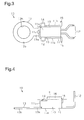
Fig. 3 is a top view of the electronic component. -
Fig. 4 is a side view of the electronic component. -
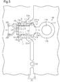
Fig. 5 is a bottom view of the electronic component when positioned in relation to the circuit board. - An electronic component according to one embodiment will now be described with reference to
Figs. 1 to 5 . - As shown in
Fig. 1 , anelectronic component 10 is joined to acircuit board 20 by reflow soldering withsolder 19, which functions as a conductor, to be mounted on thecircuit board 20. Thecircuit board 20, on which theelectronic component 10 is mounted, is arranged at a predetermined position in relation to a plate-shaped heat dissipater 30, which is a connecting member different from thecircuit board 20. - The
heat dissipater 30 is made of metal such as aluminum. Theheat dissipater 30 has in it a fluid passage (not shown), through which fluid, for example, water, flows as a cooling medium. Theheat dissipater 30 draws heat transferred from a part such as thecircuit board 20 to theheat dissipater 30 with the fluid passing through the fluid passage. - The
electronic component 10 includes amain body 11, a pair ofelectrodes 12, and a connectingportion 13. Theelectrodes 12 are provided on themain body 11 and joined to thecircuit board 20 by reflow soldering. The connectingportion 13 is provided on themain body 11 and connected to aboss portion 30a of theheat dissipater 30. The connectingportion 13 is fastened to theboss portion 30a with abolt 31. In the present embodiment, theelectronic component 10 is a thermistor (a water temperature sensor), which is used to measure the temperature of theheat dissipater 30, specifically, the temperature of the fluid passing through the fluid passage. - As shown in
Fig. 2 , themain body 11 includes abottom plate portion 11 a, which is rectangular in a plan view, and two longside plate portions 11 b, which extend from the two long sides of thebottom plate portion 11 a. Each longside plate portion 11 b is shaped as a flat plate that extends in a direction perpendicular to thebottom plate portion 11 a. The two longside plate portions 11 b extend in parallel. Themain body 11 further includes two shortside plate portions 11c, which correspond to the longside plate portions 11 b. The two shortside plate portions 11c extend toward each other from edges of the longside plate portions 11 b on one side in the longitudinal direction. Each shortside plate portion 11c is shaped as a flat plate that extends in a direction perpendicular to the corresponding longside plate portion 11 b. - Each
electrode 12 is shaped like a rod. Theelectrodes 12 extend in the longitudinal direction of thebottom plate portion 11a from the edge of thebottom plate portion 11a on the side opposite from the shortside plate portions 11c. Theelectrodes 12 are then bent to extend in the direction in which the longside plate portions 11 b project. The direction in which theelectrodes 12 protrude is the same as the longitudinal direction of thebottom plate portion 11a. - The connecting
portion 13 includes a flat plate-shaped extension 13a and anannular insertion portion 13b. Theextension 13a is integral with thebottom plate portion 11a. Theextension 13a linearly extends from the edge of thebottom plate portion 11a at which the shortside plate portions 11c are located. Theinsertion portion 13b is located at the distal end of theextension 13a. Theinsertion portion 13b has a through-hole 13h, in which thebolt 31 is allowed to be inserted. - As shown in
Fig. 3 , the longside plate portions 11 b have flat plate-shapedfirst lugs 14, which are provided on the edges opposite from thebottom plate portion 11 a and at positions closer to the shortside plate portions 11c. The flat plate-shapedfirst lugs 14 protrude outward away from each other. Also, the longside plate portions 11 b also have flat plate-shapedsecond lugs 15, which are provided on the edges opposite from the shortside plate portions 11c. The flat plate-shapedsecond lugs 15 protrude outward away from each other. Thefirst lugs 14 and thesecond lugs 15 protrude in directions perpendicular to the direction in which theelectrodes 12 protrude. - As shown in
Fig. 4 , the end faces of thefirst lugs 14 on the side opposite from thebottom plate portion 11a and the end faces of thesecond lugs 15 on the side opposite from thebottom plate portion 11a are located on a common plane, which is an imaginary plane H extending in parallel with thebottom plate portion 11a. The longside plate portions 11 b haveprotrusions 16, which are provided on the side opposite from thebottom plate portion 11a and between thefirst lugs 14 and thesecond lugs 15. Theprotrusions 16 protrude beyond the imaginary plane H in a direction opposite from thebottom plate portion 11a. - As shown in
Fig. 5 , thecircuit board 20 includes afirst circuit board 21 and asecond circuit board 22. Thefirst circuit board 21 has twoinsertion holes 20h, in which theelectrodes 12 are allowed to be inserted. Thesecond circuit board 22 is arranged side by side with thefirst circuit board 21 in a planar direction. The diameter of theinsertion holes 20h is set greater than the outer diameter of theelectrodes 12. Thefirst circuit board 21 and thesecond circuit board 22 are coupled to each other at parts of the opposed outer edges bycoupling portions 23. Thefirst circuit board 21 has arecess 21 a, which is recessed in a trapezoidal shape from the outer edge. Further, thefirst circuit board 21 has acutout portion 21 b, which is continuous with therecess 21 a and has a substantially rectangular shape in a plan view. - The
second circuit board 22 has atrapezoidal protuberance 22a, which protrudes toward therecess 21 a of thefirst circuit board 21. Theprotuberance 22a has a distal end 221 a, and thecutout portion 21 b has an inner bottom portion 211b, which is opposed to the distal end 221 a. The distance L1 between the distal end 221 a and the inner bottom portion 211 b is equal to the length L2 of eachprotrusion 16 in the longitudinal direction (indicated by the broken lines inFig. 5 ). Thecutout portion 21 b has two opposedinner sides 212b. The distance L3 between theinner sides 212b is equal to the distance L4 betweenouter surfaces 16a of theprotrusions 16. Thus, theprotrusions 16 are configured to be fit between thecutout portion 21 b and theprotuberance 22a. That is, in the present embodiment, thecircuit board 20 has a receiving portion, which is constituted by thecutout portion 21 b and theprotuberance 22a to receive theprotrusions 16. Theprotrusions 16 constitute fitting portions, which are fitted to the receiving portion. - The first lugs 14 contact the back side of the
protuberance 22a of thesecond circuit board 22, that is, the back side of thecircuit board 20, which is one of the surfaces of thecircuit board 20. The second lugs 15 contact the back side of thefirst circuit board 21 at a position on the opposite side of the inner bottom portion 211 b from therecess 21 a of thecutout portion 21 b, that is, the back side of thecircuit board 20, which is one of the surfaces of thecircuit board 20. Thus, thefirst lugs 14 and thesecond lugs 15 function as contacting portions, which are allowed to contact the back side of thecircuit board 20. Therefore, in the present embodiment, themain body 11 has four contacting portions that are allowed to contact the back side of thecircuit board 20. - The first lugs 14 and the
second lugs 15 are arranged in relation to themain body 11 such that a region Z surrounded by thelugs 14, 15 (indicated by the long dashed double-short dashed lineFig. 5 ) contains a part of themain body 11. The region Z is a rectangular region in a plan view, which is surrounded by straight lines that connect substantially centers of parts of thefirst lugs 14 and thesecond lugs 15 that contact the back side of thecircuit board 20. - Operation of the present embodiment will now be described. A process will also be described in which the
electronic component 10 is mounted on thecircuit board 20, and the connectingportion 13 is fastened to theboss portion 30a with thebolt 31. - First, the
electronic component 10 is arranged on the back side of thecircuit board 20 such that theprotrusions 16 are fitted between thecutout portion 21 b and theprotuberance 22a. At this time, eachelectrode 12 is inserted in thecorresponding insertion hole 20h. Fitting theprotrusions 16 between thecutout portion 21 b and theprotuberance 22a causes the ends of theprotrusions 16 in the vicinity of thefirst lugs 14 to contact the distal end 221 a of theprotuberance 22a. The ends of theprotrusions 16 that are close to thesecond lugs 15 contact the inner bottom portion 211 b of thecutout portion 21 b. Further, fitting theprotrusions 16 between thecutout portion 21 b and theprotuberance 22a causes theouter surfaces 16a of theprotrusions 16 to contact theinner sides 212b of thecutout portion 21 b. Accordingly, the position of thecircuit board 20 in the planar direction on theelectronic component 10 is defined. - Also, the
first lugs 14 contact the back side of theprotuberance 22a of thesecond circuit board 22. The second lugs 15 contact the back side of thefirst circuit board 21 at a position on the opposite side of the inner bottom portion 211 b from therecess 21 a of thecutout portion 21 b. Accordingly, the position of thecircuit board 20 in the thickness direction of theelectronic component 10 is defined. - The end faces of the
first lugs 14 that are on the opposite side from thebottom plate portion 11 a and the end faces of thesecond lugs 15 that are on the opposite side from thebottom plate portion 11 a are on the common plane. Thus, the positions at which thefirst lugs 14 and thesecond lugs 15 contact the back side of thecircuit board 20 are located on the common plane. Further, thefirst lugs 14 and thesecond lugs 15 are arranged in relation to themain body 11 such that a region Z surrounded by thelugs main body 11. Thus, when thefirst lugs 14 and thesecond lugs 15 contact the back side of thecircuit board 20, the imaginary plane H of the region Z is parallel with the back side of thecircuit board 20. Therefore, the orientation of theelectronic component 10 is prevented from being inclined with respect to the back side of thecircuit board 20. - Then, joining the
electrodes 12 to thecircuit board 20 by reflow soldering mounts theelectronic component 10 on thecircuit board 20. At this time, theelectronic component 10 is positioned in relation to thecircuit board 20 by theprotrusions 16 being fitted between thecutout portion 21 b and theprotuberance 22a and thefirst lugs 14 and thesecond lugs 15 contacting the back side of thecircuit board 20. Theelectrodes 12 are thus restrained from being moved by the surface tension of solder caused by reflow soldering. As a result, when thecircuit board 20, on which theelectronic component 10 is mounted, is arranged at a predetermined position in relation to theheat dissipater 30, the position of the connectingportion 13
is restrained from being displaced in relation to theboss portion 30a, to which theheat dissipater 30 is connected. The connectingportion 13 is fastened to theboss portion 30a with thebolt 31 after thesecond circuit board 22 is separated from thefirst circuit board 21 by cutting thecoupling portions 23. - The above described embodiment provides the following advantages.
- (1) The
cutout portion 21 b and theprotuberance 22a constitute a receiving portion in thecircuit board 20. Theelectronic component 10 includes a pair ofprotrusions 16, which is fitted between thecutout portion 21 b and theprotuberance 22a, a pair offirst lugs 14, and a pair ofsecond lugs 15. The first lugs 14 and thesecond lugs 15 contact the back side of thecircuit board 20. With this configuration, fitting theprotrusions 16 between thecutout portion 21 b and theprotuberance 22a defines the position of thecircuit board 20 in the planar direction on theelectronic component 10. Also, causing thefirst lugs 14 and thesecond lugs 15 to contact the back side of thecircuit board 20 defines the position of thecircuit board 20 in the thickness direction in theelectronic component 10. As a result, when thecircuit board 20, on which theelectronic component 10 is mounted, is arranged at a predetermined position in relation to theheat dissipater 30, the position of the connectingportion 13 is restrained from being displaced in relation to theboss portion 30a, to which the connecting member is connected. - (2) The positions at which the
first lugs 14 and thesecond lugs 15 contact the back side of thecircuit board 20 are located on the common plane. The first lugs 14 and thesecond lugs 15 are arranged in relation to themain body 11 such that a region Z surrounded by thelugs main body 11. Accordingly, when thefirst lugs 14 and thesecond lugs 15 contact the back side of thecircuit board 20, the imaginary plane H of the region Z, which is surrounded by thelugs circuit board 20. Therefore, the orientation of theelectronic component 10 is prevented from being inclined with respect to the back side of thecircuit board 20. - (3) For example, when the
second lugs 15 protrude in the direction in which theelectrodes 12 protrude from themain body 11, the parts of theelectrodes 12 that are inserted in theinsertion holes 20h and thesecond lugs 15 need to be separated from each other by at least the insulation distance so that the insulation between the inserted parts and the second lugs 15 is ensured. Thus, the length of a part of eachelectrode 12 from themain body 11 to theinsertion hole 20h needs to be extended by the insulation distance, which enlarges the overall size of theelectronic component 10. Thus, thesecond lugs 15, which are provided at the end close to theelectrodes 12 of themain body 11, each project in a direction perpendicular to the direction in which theelectrodes 12 protrude. Compared to a case in which thesecond lugs 15 protrude from themain body 11 in the direction in which theelectrodes 12 project, the above illustrated configuration shortens the length of a part of eachelectrode 12 from themain body 11 to theinsertion hole 20h required to ensure a sufficient insulation distance between the part of eachelectrode 12 that is inserted in thecorresponding insertion hole 20h and the correspondingsecond lug 15. This restrains the overall size of theelectronic component 10 from being enlarged. - (4) Each
electrode 12 is joined to thecircuit board 20 by reflow soldering. Theelectrodes 12 are thus restrained from being moved by the surface tension of thesolder 19 caused by reflow soldering. - (5) Since the position of the connecting
portion 13 of theelectronic component 10 is restrained from being displaced in relation to theboss portion 30a of theheat dissipater 30, the fastening of the connectingportion 13 to theboss portion 30a with thebolt 31 can be automated. - The above described embodiment may be modified as follows.
- In the illustrated embodiment, the
first lugs 14 may be omitted. In this case, on the edge of each longside plate portion 11 b opposite from thebottom plate portion 11 a, a part closer to the corresponding shortside plate portion 11c functions as a contacting portion, which is allowed to contact the back side of thecircuit board 20. - In the illustrated embodiment, although the number of contacting portions, which are allowed to contact the back side of the
circuit board 20, is not particularly limited, themain body 11 preferably has three or more contacting portions. - In the illustrated embodiment, as long as the
first lugs 14 and thesecond lugs 15 project in directions intersecting the direction in which theelectrodes 12 protrude, the angles relative to the protruding direction of theelectrodes 12 are not particularly limited. - In the illustrated embodiment, the
first lugs 14 may protrude in the direction in which theextension 13a extends from thebottom plate portion 11a. - In the illustrated embodiment, the
second lugs 15 may protrude in the direction in which theelectrodes 12 protrude from themain body 11. - In the illustrated embodiment, the connecting
portion 13 and theboss portion 30a may be connected, for example, by an adhesive. - In the illustrated embodiment, the
electronic component 10 may be a chip that is surface-mounted on thecircuit board 20. - In the illustrated embodiment, although the
heat dissipater 30 is employed as a connecting member connected to the connectingportion 13, the connecting member is not particularly limited. - In the illustrated embodiment, the region Z may be a region that is surrounded by curves that connect substantially centers of parts of the
first lugs 14 and thesecond lugs 15 that contact the back side of thecircuit board 20. - In the illustrated embodiment, the region Z may be a region that is surrounded by straight lines or curves that connect edges of parts of the
first lugs 14 and thesecond lugs 15 that contact the back side of thecircuit board 20. - In the illustrated embodiment, the
second circuit board 22 does not necessary need to be separated from the first circuit board when the connectingportion 13 is fastened to theboss portion 30a with thebolt 31. In this case, thesecond circuit board 22 needs to have a through-hole for receiving thebolt 31. - In the illustrated embodiment, the
electrodes 12 may be joined to thecircuit board 20 by a soldering method other than reflow soldering. - In the illustrated embodiment, the
electrodes 12 may be joined to thecircuit board 20 with an electrically conductive adhesive, which serves as a conductor.
Claims (7)
- An electronic component comprising:a main body; andan electrode, which is provided on the main body and is configured to be joined to a circuit board with a conductor,wherein the main body includesa connecting portion, which is configured to be connected to a connecting member,a fitting portion, which is allowed to be fitted to a receiving portion provided in the circuit board, anda contacting portion, which is allowed to contact a surface of the circuit board.
- The electronic component according to claim 1, wherein
in addition to the contacting portion, the main body includes two or more additional contacting portions,
positions at which the contacting portions contact the surface of the circuit board are located on a common plane, and
the contacting portions are arranged in relation to the main body such that a region surrounded by the contacting portions contains at least a part of the main body. - The electronic component according to claim 1, wherein
the electrode protrudes from the main body and is allowed to be inserted in an insertion hole provided in the circuit board, and
the contacting portion is located at an end of the main body that is close to the electrode, and the contacting portion protrudes in a direction intersecting a direction in which the electrode protrudes. - The electronic component according to claim 2, wherein
the electrode extends from the main body and is allowed to be inserted in an insertion hole provided in the circuit board,
at least one of the contacting portions is located at an end of the main body that is close to the electrode, and
the at least one of the contacting portions extends in a direction intersecting a direction in which the electrode extends. - The electronic component according to any one of claims 1 to 4, wherein the electrode is joined to the circuit board by reflow soldering.
- The electronic component according to any one of claims 1 to 5, wherein the connecting member is a heat dissipater, which dissipates heat transferred from the circuit board.
- The electronic component according to any one of claims 1 to 6, wherein the electronic component is a thermistor.
Applications Claiming Priority (2)
| Application Number | Priority Date | Filing Date | Title |
|---|---|---|---|
| JP2013269562A JP5729462B1 (en) | 2013-12-26 | 2013-12-26 | Electronic components |
| PCT/JP2014/082574 WO2015098503A1 (en) | 2013-12-26 | 2014-12-09 | Electronic component |
Publications (2)
| Publication Number | Publication Date |
|---|---|
| EP3089566A1 true EP3089566A1 (en) | 2016-11-02 |
| EP3089566A4 EP3089566A4 (en) | 2016-11-23 |
Family
ID=53437936
Family Applications (1)
| Application Number | Title | Priority Date | Filing Date |
|---|---|---|---|
| EP14874338.8A Withdrawn EP3089566A4 (en) | 2013-12-26 | 2014-12-09 | Electronic component |
Country Status (6)
| Country | Link |
|---|---|
| US (1) | US20160314879A1 (en) |
| EP (1) | EP3089566A4 (en) |
| JP (1) | JP5729462B1 (en) |
| CN (1) | CN105830543A (en) |
| TW (1) | TW201532082A (en) |
| WO (1) | WO2015098503A1 (en) |
Families Citing this family (2)
| Publication number | Priority date | Publication date | Assignee | Title |
|---|---|---|---|---|
| JP7152160B2 (en) | 2018-01-26 | 2022-10-12 | 矢崎総業株式会社 | Busbar and busbar fixing structure |
| JP7181013B2 (en) * | 2018-06-20 | 2022-11-30 | Juki株式会社 | Electronic component mounting apparatus and electronic component mounting method |
Family Cites Families (13)
| Publication number | Priority date | Publication date | Assignee | Title |
|---|---|---|---|---|
| JPS624974Y2 (en) * | 1979-12-19 | 1987-02-04 | ||
| JPS58113285U (en) * | 1982-01-27 | 1983-08-02 | クラリオン株式会社 | Mounting structure of socket on board |
| JPH11233910A (en) | 1998-02-10 | 1999-08-27 | Nec Saitama Ltd | Component mounting method |
| JP3666278B2 (en) * | 1999-01-14 | 2005-06-29 | 松下電器産業株式会社 | Electronic component and wiring board for mounting the same |
| TW415457U (en) * | 1999-06-10 | 2000-12-11 | Chen Ching Jia | Auto injector for fluid vessel |
| JP2006147938A (en) * | 2004-11-22 | 2006-06-08 | Fuji Photo Film Co Ltd | Electronic component mounting method, electronic component, and module with electronic component mounted therein |
| US7465088B2 (en) * | 2006-06-22 | 2008-12-16 | Microsoft Corporation | Thermal sensing system |
| JP4300371B2 (en) * | 2007-11-14 | 2009-07-22 | オンキヨー株式会社 | Semiconductor device |
| JP2009181775A (en) * | 2008-01-30 | 2009-08-13 | Toyota Industries Corp | Terminal structure |
| JP5067437B2 (en) * | 2010-03-19 | 2012-11-07 | 株式会社安川電機 | Electronic component mounting structure, power conversion device using the mounting structure, and electronic component mounting method |
| TWM415457U (en) * | 2011-04-20 | 2011-11-01 | Cal Comp Electronics & Comm Co | Vertical connector and assembly thereof |
| KR101946259B1 (en) * | 2011-05-31 | 2019-02-12 | 삼성전기 주식회사 | Multilayer ceramic electronic component |
| JP2013222766A (en) * | 2012-04-13 | 2013-10-28 | Nippon Soken Inc | Mounting substrate |
-
2013
- 2013-12-26 JP JP2013269562A patent/JP5729462B1/en not_active Expired - Fee Related
-
2014
- 2014-12-09 US US15/104,893 patent/US20160314879A1/en not_active Abandoned
- 2014-12-09 CN CN201480069857.7A patent/CN105830543A/en active Pending
- 2014-12-09 EP EP14874338.8A patent/EP3089566A4/en not_active Withdrawn
- 2014-12-09 WO PCT/JP2014/082574 patent/WO2015098503A1/en not_active Ceased
- 2014-12-23 TW TW103144899A patent/TW201532082A/en unknown
Also Published As
| Publication number | Publication date |
|---|---|
| JP5729462B1 (en) | 2015-06-03 |
| US20160314879A1 (en) | 2016-10-27 |
| JP2015126109A (en) | 2015-07-06 |
| CN105830543A (en) | 2016-08-03 |
| EP3089566A4 (en) | 2016-11-23 |
| WO2015098503A1 (en) | 2015-07-02 |
| TW201532082A (en) | 2015-08-16 |
Similar Documents
| Publication | Publication Date | Title |
|---|---|---|
| US8840408B2 (en) | Crank-shaped board terminal with a protruding support portion | |
| US9653853B2 (en) | Electrical connection box including a circuit substrate | |
| US9462731B2 (en) | Cover structure for electronic circuit module | |
| KR102364833B1 (en) | Fuse for an electrical circuit and printed circuit board having a fuse | |
| US10429137B2 (en) | Heat sink | |
| US10263405B2 (en) | Circuit assembly and electrical junction box | |
| JP6464270B2 (en) | Plug connector | |
| US20140299893A1 (en) | Conductive Connector For Use With Circuit Board, and LED Module Having the Same | |
| JP6330690B2 (en) | Board unit | |
| CN106796934A (en) | Semiconductor device | |
| US20190082527A1 (en) | Circuit structure | |
| US9585263B2 (en) | Pin to PCB connection structure and method | |
| US20160314879A1 (en) | Electronic component | |
| JP6638262B2 (en) | Circuit components | |
| JP6287659B2 (en) | Circuit structure | |
| US9942988B2 (en) | Circuit board and power supply apparatus | |
| JP5652736B2 (en) | Terminal box | |
| US20100254091A1 (en) | Fixation structure for connector of in-vehicle controller | |
| US20200127399A1 (en) | Pin header | |
| US20110310573A1 (en) | High frequency device and a printed board holding structure | |
| US9258881B2 (en) | SMT heat sink anchor | |
| JP2011254647A (en) | Electrical junction box | |
| US20130208425A1 (en) | Electronic Device having a Housing Made of Profile Material | |
| TWI658760B (en) | Large current printed circuit board | |
| KR101935285B1 (en) | Electronic element having lead terminal with positive temporary fixing on PCB plate |
Legal Events
| Date | Code | Title | Description |
|---|---|---|---|
| PUAI | Public reference made under article 153(3) epc to a published international application that has entered the european phase |
Free format text: ORIGINAL CODE: 0009012 |
|
| 17P | Request for examination filed |
Effective date: 20160511 |
|
| AK | Designated contracting states |
Kind code of ref document: A1 Designated state(s): AL AT BE BG CH CY CZ DE DK EE ES FI FR GB GR HR HU IE IS IT LI LT LU LV MC MK MT NL NO PL PT RO RS SE SI SK SM TR |
|
| AX | Request for extension of the european patent |
Extension state: BA ME |
|
| A4 | Supplementary search report drawn up and despatched |
Effective date: 20161024 |
|
| RIC1 | Information provided on ipc code assigned before grant |
Ipc: H05K 1/18 20060101AFI20161018BHEP Ipc: H01L 21/60 20060101ALI20161018BHEP Ipc: H01C 7/04 20060101ALI20161018BHEP |
|
| DAX | Request for extension of the european patent (deleted) | ||
| STAA | Information on the status of an ep patent application or granted ep patent |
Free format text: STATUS: THE APPLICATION IS DEEMED TO BE WITHDRAWN |
|
| 18D | Application deemed to be withdrawn |
Effective date: 20170523 |