EP3089366A1 - Frequency selective circuit - Google Patents
Frequency selective circuit Download PDFInfo
- Publication number
- EP3089366A1 EP3089366A1 EP15190380.4A EP15190380A EP3089366A1 EP 3089366 A1 EP3089366 A1 EP 3089366A1 EP 15190380 A EP15190380 A EP 15190380A EP 3089366 A1 EP3089366 A1 EP 3089366A1
- Authority
- EP
- European Patent Office
- Prior art keywords
- transistor
- frequency selective
- terminal
- coupled
- selective circuit
- Prior art date
- Legal status (The legal status is an assumption and is not a legal conclusion. Google has not performed a legal analysis and makes no representation as to the accuracy of the status listed.)
- Granted
Links
Images





Classifications
-
- H—ELECTRICITY
- H03—ELECTRONIC CIRCUITRY
- H03H—IMPEDANCE NETWORKS, e.g. RESONANT CIRCUITS; RESONATORS
- H03H11/00—Networks using active elements
- H03H11/02—Multiple-port networks
- H03H11/04—Frequency selective two-port networks
- H03H11/0422—Frequency selective two-port networks using transconductance amplifiers, e.g. gmC filters
- H03H11/0461—Current mode filters
-
- H—ELECTRICITY
- H03—ELECTRONIC CIRCUITRY
- H03H—IMPEDANCE NETWORKS, e.g. RESONANT CIRCUITS; RESONATORS
- H03H11/00—Networks using active elements
- H03H11/02—Multiple-port networks
- H03H11/04—Frequency selective two-port networks
- H03H11/0422—Frequency selective two-port networks using transconductance amplifiers, e.g. gmC filters
-
- H—ELECTRICITY
- H03—ELECTRONIC CIRCUITRY
- H03F—AMPLIFIERS
- H03F3/00—Amplifiers with only discharge tubes or only semiconductor devices as amplifying elements
- H03F3/45—Differential amplifiers
- H03F3/45071—Differential amplifiers with semiconductor devices only
- H03F3/45076—Differential amplifiers with semiconductor devices only characterised by the way of implementation of the active amplifying circuit in the differential amplifier
- H03F3/45179—Differential amplifiers with semiconductor devices only characterised by the way of implementation of the active amplifying circuit in the differential amplifier using MOSFET transistors as the active amplifying circuit
- H03F3/45273—Mirror types
-
- H—ELECTRICITY
- H03—ELECTRONIC CIRCUITRY
- H03H—IMPEDANCE NETWORKS, e.g. RESONANT CIRCUITS; RESONATORS
- H03H11/00—Networks using active elements
- H03H11/02—Multiple-port networks
- H03H11/04—Frequency selective two-port networks
- H03H11/0405—Non-linear filters
-
- H—ELECTRICITY
- H03—ELECTRONIC CIRCUITRY
- H03H—IMPEDANCE NETWORKS, e.g. RESONANT CIRCUITS; RESONATORS
- H03H11/00—Networks using active elements
- H03H11/02—Multiple-port networks
- H03H11/04—Frequency selective two-port networks
- H03H11/0416—Frequency selective two-port networks using positive impedance converters
-
- H—ELECTRICITY
- H03—ELECTRONIC CIRCUITRY
- H03H—IMPEDANCE NETWORKS, e.g. RESONANT CIRCUITS; RESONATORS
- H03H11/00—Networks using active elements
- H03H11/02—Multiple-port networks
- H03H11/04—Frequency selective two-port networks
- H03H11/0422—Frequency selective two-port networks using transconductance amplifiers, e.g. gmC filters
- H03H11/0466—Filters combining transconductance amplifiers with other active elements, e.g. operational amplifiers, transistors, voltage conveyors
-
- H—ELECTRICITY
- H03—ELECTRONIC CIRCUITRY
- H03H—IMPEDANCE NETWORKS, e.g. RESONANT CIRCUITS; RESONATORS
- H03H11/00—Networks using active elements
- H03H11/02—Multiple-port networks
- H03H11/04—Frequency selective two-port networks
- H03H11/12—Frequency selective two-port networks using amplifiers with feedback
- H03H11/1213—Frequency selective two-port networks using amplifiers with feedback using transistor amplifiers
-
- H—ELECTRICITY
- H03—ELECTRONIC CIRCUITRY
- H03F—AMPLIFIERS
- H03F2200/00—Indexing scheme relating to amplifiers
- H03F2200/91—Indexing scheme relating to amplifiers the amplifier has a current mode topology
-
- H—ELECTRICITY
- H03—ELECTRONIC CIRCUITRY
- H03H—IMPEDANCE NETWORKS, e.g. RESONANT CIRCUITS; RESONATORS
- H03H11/00—Networks using active elements
- H03H11/02—Multiple-port networks
- H03H11/04—Frequency selective two-port networks
- H03H11/0405—Non-linear filters
- H03H2011/0411—Rank order or median filters
Definitions
- the disclosure relates in general to a frequency selective circuit.
- the frequency selective circuit such as the low pass filter (LPF)
- LPF low pass filter
- an inphase/quadrature modulator (IQM) may cooperate with a simple LPF cascaded by passive RC (resistor, capacitor) filters to generate signals to be transmitted. Once the frequency of unwanted signal is close to the desired signal, such LPF cannot provide enough rejections because of the low Q.
- IQM inphase/quadrature modulator
- the designer needs to cascade more stages of RC filters, which occupied larger area, generates lager output noise and may corrupt the desired signal.
- the disclosure is directed to a frequency selective circuit capable of performing high Q filtering and reducing the output noise.
- a frequency selective circuit includes a first transistor, an impedance element, a first capacitive element, a second capacitive element, a second capacitive and a second transistor.
- the first transistor includes a first terminal, a second terminal and a control terminal.
- the impedance element is coupled between the first terminal and the control terminal of the first transistor.
- the first capacitive element is coupled to the first terminal of the first transistor.
- the second capacitive element is coupled to the control terminal of the first transistor.
- the second transistor includes a first terminal, a second terminal and a control terminal, wherein the control terminal of the second transistor is coupled to the control terminal of the first transistor.
- FIG. 1 shows the circuit diagram of a frequency selective circuit 100 according to an embodiment of the present invention.
- the frequency selective circuit 100 includes a first transistor M 1 , an impedance element ZA1, a first capacitive element C 1 , a second capacitive element C 2 and a second transistor M 2 .
- the impedance element ZA1 includes a resistive element such as the resistor R 1 .
- the impedance element ZA1 is coupled between the drain and gate of the first transistor M 1 .
- the first capacitive element C 1 is coupled to the drain of the first transistor M 1 .
- the gate of the first transistor M 1 is coupled to the second capacitive element C 2 and the gate of the second transistor M 2 .
- the first and second capacitive elements C 1 and C 2 can be implemented by capacitors for example.
- the drain of the first transistor M 1 is further coupled to the input current I i , and thus a control voltage V o is induced on the gate of the second transistor M 2 .
- the second transistor M 2 In response to the control voltage V o , the second transistor M 2 generates the output current I o at its drain.
- the frequency selective circuit 100 can be regarded as a 2 nd order current-mode filter.
- the Q-factor can be larger than 0.5. That is, the frequency selective circuit 100 is capable of perform a high Q filtering. Further, it can be obtained from FIG. 1 that, an additional cascode stage is unnecessary for the frequency selective circuit 100, and hence the voltage headroom can be enlarged.
- the impedance element coupled to the first transistor may include at least one of a resistive element (e.g., a resistor) and an inductive element (e.g., an inductor).
- FIG. 2 shows the circuit diagram of a frequency selective circuit 200 according to an alternative embodiment of the present invention.
- denotations in FIG. 2 that are same as those in FIG. 1 represent elements, materials or substances that are functionally identical or similar, and associated details are omitted herein.
- elements with the same denotations may be implemented by different circuits, materials or structures.
- the impedance element ZA2 includes a resistor R 1 and an inductor L 1 in series.
- L 1 represents the inductance of the inductor L 1 .
- the out-band rejections of the frequency selective circuit 200 can be further improved by appropriately choosing the pole frequency ⁇ PL .
- FIG. 3 shows the circuit diagram of a frequency selective circuit 300 according to an alternative embodiment of the present invention.
- the main difference between the frequency selective circuit 300 and the frequency selective circuit 200 shown in FIG. 2 is that the impedance element ZA3 includes inductor(s) L 1 only.
- the frequency selective circuit may cascade multiple sub-circuits to perform high-order filtering.
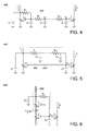
- FIG. 4 shows the circuit diagram of a frequency selective circuit 400 according to an alternative embodiment of the present invention.
- the frequency selective circuit 400 includes multiple sub-circuits 402 cascaded between the gates of the first and second transistors M 1 and M 2 .
- the sub-circuits 402 can be implemented by various types of filters. For example, in FIG. 4 , each sub-circuit 402 includes a RC filter.
- C 3 to C n respectively represent the capacitances of the capacitors C 3 to C n
- R 2 to R n -1 respectively represent the resistances of the resistors R 2 to R n-1 .
- FIG. 5 shows the circuit diagram of a frequency selective circuit 500 according to an alternative embodiment of the present invention.
- the frequency selective circuit 500 employs the multiple sub-circuits 502 in its impedance element ZA5.
- the impedance element ZA5 includes multiple sub-circuits 502 cascaded in series. Similar to the sub-circuits 402 shown in FIG. 4 , each sub-circuit 502 can be formed by a RC filter, but it is understood that the present is not limited thereto.
- FIG. 6 shows the circuit diagram of a frequency selective circuit 600 according to an alternative embodiment of the present invention.
- the impedance element ZA6 of the frequency selective circuit 600 further includes a third transistor M 3 for a low input swing design.
- the drain of the third transistor M 3 is coupled to the gate of the first transistor M 1 via the resistor R 1 .
- the source of the third transistor M 3 is coupled to the drain of the first transistor M 1 .
- the gate of the third transistor M 3 is biased by a reference voltage V b .
- FIG. 7 shows the circuit diagram of a frequency selective circuit 700 according to an alternative embodiment of the present invention.
- the main difference between the frequency selective circuit 700 and the frequency selective circuit 600 shown in FIG. 6 is that the resistor R 1 is removed from the impedance element ZA7.
- g m 3 represents the transconductance of the third transistor M 3 .
- the frequency selective circuit 700 has more design freedom since the first and second capacitive elements C 1 and C 2 are isolated by the third transistor M 3 . Once the third transistor is biased at the linear region, the transfer function returns to eq1.
- FIG. 8 shows the circuit diagram of a frequency selective circuit 800 according to an alternative embodiment of the present invention.
- the impedance element ZA8 of the frequency selective circuit 800 further includes an operational amplifier 802 to reduce the input swing.
- the operational amplifier 802 includes a first input, a second input and an output. The first input is coupled to the reference voltage V b , the second input is coupled to the source of the third transistor M 3 , and the output is coupled to the gate of the third transistor M 3 .
- the voltage at the node i.e., source of the third transistor M 3 , or drain of the first transistor M 1
- the input swing can be set to zero.
- FIG. 9 shows the circuit diagram of a frequency selective circuit 900 according to an alternative embodiment of the present invention.
- the frequency selective circuit 900 employs CMOS inverter configuration at its input stage and output stage.
- the impedance element ZA9 of the frequency selective circuit 900 includes a first complementary transistor M p1 .
- the type of the first complementary transistor M p1 is complementary to that of the first transistor M 1 .
- the first complementary transistor M p1 is a P-type transistor when the first transistor M 1 is an N-type transistor, while is an N-type transistor when the first transistor M 1 is a P-type transistor.
- the first complementary transistor M p1 and the first transistor M 1 are connected to each other based CMOS inverter configuration, wherein the drain of the first complementary transistor M p1 is coupled to the drain of the first transistor M 1 , and the gate of the first complementary transistor M p1 is coupled to the gate and of the first transistor M 1 .
- the frequency selective circuit 900 includes a second complementary transistor M p2 coupled to the second transistor M 2 and forming a CMOS inverter together with the second transistor M 2 .
- the impedance element ZA9 further includes a resistive element, e.g., the resistor R 1 , coupled between the drain and gate of the first complementary transistor M P1 .
- g M 1 is the equivalent transconductance of the transconductances of the first complementary transistor M p1 and the first transistor M 1
- g M 2 is the equivalent transconductance of the transconductances of the second complementary transistor M p2 and the second transistor M 2 .
- the equivalent transconductances g M 1 and g M2 are twice with the same current consumption.
- FIG. 10 shows the circuit diagram of a frequency selective circuit 1000 according to an alternative embodiment of the present invention.
- the frequency selective circuit 1000 employs differential configuration at its input and output stages.
- the frequency selective circuit 1000 includes an input differential pair 1002 at the input stage and an output differential pair 1004 at the output stage.
- the output differential pair 1004 may generate output currents I op and I on in response to the input currents I ip and I in received from the input differential pair 1002.
- the input differential pair 1002 includes two branches B i1 and B i2 .
- the branch B i1 includes a transistor M 1p , a resistor R 1P and a capacitor C 2p .
- the drain of the transistor M 1p is coupled to its gate via the resistor R 1P , and the gate of the transistor M 1P is further coupled to the capacitor C 2p .
- the branch B i2 includes a transistor M 1n , a resistor R 1n and a capacitor C 2n .
- the drain of the transistor M 1n is coupled to its gate via the resistor R 1n , and the gate of the transistor M 1n is further coupled to the capacitor C 2n .
- a capacitor C 1 ' is coupled between the drains of the transistors M 1p and M 1n .
- the input differential pair 1002 can be regarded as a differential form of the left part of the frequency selective circuit 100 shown in FIG. 1 . That is, the first transistor M 1 , the impedance element ZA1 and the second capacitive element C 2 can be used to form one branch B i1 / B i2 of the input differential pair 1002, and the branch B i1 / B i2 is coupled to the paired branch B i2 / B i1 via the first capacitive element C 1 .
- the output differential pair 1004 includes two branches B o1 and B o2 .
- the branch B o1 includes a transistor M 2p to induce the output current I op
- the branch B o2 includes a transistor M 2n to induce the output current I on .
- the output differential pair 1004 can be regarded as the differential form of the right part of the frequency selective circuit 100.
- the second transistor M 2 can be used to form one branch B o1 / B o2 of the output differential pair 1004, and the branch B o1 / B o2 is coupled to the paired branch B o2 / B o1 via the source of the second transistor M 2 .
- the transfer function of the frequency selective circuit 1000 has the same form as that of the frequency selective circuit 100 shown in FIG. 1 , but the capacitance of the capacitor C 1 ' can be half of C 1 .
- FIG. 11 shows the circuit diagram of a frequency selective circuit 1100 according to an alternative embodiment of the present invention.
- two branches B i1 ' and B i2 ' of the input differential pair 1102 are coupled to each other further via a capacitor C 2 '.
- the gate of the transistor M 1p is coupled to the gate of the transistor of M 1n via the capacitor C 2 '.
- the transfer function of the frequency selective circuit 1100 has the same form as equation eq1, and the capacitance of the capacitor C 2 ' can be half of the capacitance of the capacitor C 2 .
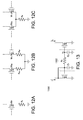
- the source degeneration technique can be used to improve the linearity of the circuit.
- the source of the first/second transistor M 1 /M 2 is coupled to a degeneration resistive element R d .
- a degeneration resistive element R d For a differential pair, two degeneration resistive elements R dp and R dn can be added to the sources of the transistors M 1P /M 2P and M 1n /M 2n , respectively, as shown in FIG. 12B .
- the sources of the transistors M 1P /M 2P and M 1n /M 2n can be commonly coupled to the same degeneration resistive element R d , as shown in FIG. 12C .
- FIG. 13 illustrates the circuit diagram of a frequency selective circuit 1300 that the first transistor M1 is diode-connected and a 2 nd order LPF 1302 is coupled between the gates of the first and second transistors M 1 and M 2 .
- the Q-factor is smaller than 0.5, which could not provide large rejection.
- k' is a constant associated to temperature
- the in-band output noise of the frequency selective circuit 100 is much smaller than that of the frequency selective circuit 1300, which proves that the proposed frequency selective circuit has better noise reduction performance.
- FIG. 14A illustrates a simulated frequency response of a Butterworth filter implemented by the proposed frequency selective circuit.
- FIG. 14B illustrates a simulated frequency response of a low pass filter implemented by the frequency selective circuit shown in FIG. 13 .
- the rejection at 64MHz of the proposed frequency selective circuit is at least 7dB better than that of the frequency selective circuit 1300, and the in-band roll-off of the proposed frequency selective circuit is also smaller.
- FIG. 15 shows the block diagram of a transmitter (TX) 1500 according to an embodiment of the present invention.
- the TX 1500 includes a digital-to-analog converter (DAC) 1502, a current mode filter (CMF) 1504, an inphase/quadrature modulator (IQM) 1506, a driving amplifier (DA) 1508 and a power amplifier (PA) 1510 and an antenna 1512.
- the CMF 1504 can be implemented by any of the proposed frequency selective circuits and is used as a TX baseband filter. With the help of the proposed frequency selective circuit, high Q filtering without any extra current consumption can be achieved.
- FIG. 16 shows the block diagram of a receiver (RX) 1600 according to an embodiment of the present invention.
- the RX 1600 includes an antenna 1602, a low noise amplifier (LNA) 1604, a mixer 1606, a CMF 1610, a tansimpedance amplifier (TIA) 1610 and an analog-to-digital converter 1612.
- the CMF 1608 can be implemented by any of the frequency selective circuits described above and is used as a RX baseband filter.
- the current-mode signal needs to be transferred to voltage domain by the TIA.
- the CMF 1610 is placed before the TIA 1610, which relaxes the TIA design and improves the current consumption.
- FIG. 17 shows the block diagram of a RX 1700 according to an embodiment of the present invention.
- the RX 1700 further includes a CMF 1702 cooperating with the LNA 1604.
- the CMF 1702 can be implemented by any of the proposed frequency selective circuits described above, and is used as a radio frequency (RF) filter based on the naturally wideband characteristic from current mode.
- the CMF 1702 can be embedded into the LNA 1604 and co-designed together.
- the present invention provides a frequency selective circuit which mainly includes a first transistor, an impedance element, a first capacitive element, a second capacitive element and a second transistor.
- the first transistor includes a first terminal (e.g, the drain/source), a second terminal (e.g., the source/drain) and a control terminal (e.g., the gate).
- the impedance element is coupled between the first terminal and the control terminal of the first transistor.
- the first capacitive element is coupled to the first terminal of the first transistor.
- the second capacitive element is coupled to the control terminal of the first transistor.
- the second transistor includes a first terminal, a second terminal and a control terminal coupled to the control terminal of the first transistor.
- the proposed frequency selective circuit exhibits excellent close-in rejections and noise performance. Further, the in-band roll-off of the proposed frequency can be much better than conventional cascaded RC LPF. In addition, the proposed frequency selective circuit needs not consume additional current, which is favored in low power design for portable design.
Landscapes
- Engineering & Computer Science (AREA)
- Power Engineering (AREA)
- Physics & Mathematics (AREA)
- Nonlinear Science (AREA)
- Networks Using Active Elements (AREA)
- Amplifiers (AREA)
Abstract
Description
- The disclosure relates in general to a frequency selective circuit.
- In modern circuit designs, the frequency selective circuit, such as the low pass filter (LPF), is an indispensable block for filtering signals. For example, an inphase/quadrature modulator (IQM) may cooperate with a simple LPF cascaded by passive RC (resistor, capacitor) filters to generate signals to be transmitted. Once the frequency of unwanted signal is close to the desired signal, such LPF cannot provide enough rejections because of the low Q.
- For getting better rejections, the designer needs to cascade more stages of RC filters, which occupied larger area, generates lager output noise and may corrupt the desired signal.
- Therefore, there is a need of a frequency selective circuit capable of performing high Q filtering and reducing the output noise.
- The disclosure is directed to a frequency selective circuit capable of performing high Q filtering and reducing the output noise.
- According to one embodiment, a frequency selective circuit is provided. The frequency selective circuit includes a first transistor, an impedance element, a first capacitive element, a second capacitive element, a second capacitive and a second transistor. The first transistor includes a first terminal, a second terminal and a control terminal. The impedance element is coupled between the first terminal and the control terminal of the first transistor. The first capacitive element is coupled to the first terminal of the first transistor. The second capacitive element is coupled to the control terminal of the first transistor. The second transistor includes a first terminal, a second terminal and a control terminal, wherein the control terminal of the second transistor is coupled to the control terminal of the first transistor.
-
-
FIG. 1 shows the circuit diagram of a frequency selective circuit according to an embodiment of the present invention. -
FIG. 2 shows the circuit diagram of a frequency selective circuit according to an alternative embodiment of the present invention. -
FIG. 3 shows the circuit diagram of a frequency selective circuit according to an alternative embodiment of the present invention. -
FIG. 4 shows the circuit diagram of a frequency selective circuit according to an alternative embodiment of the present invention. -
FIG. 5 shows the circuit diagram of a frequency selective circuit according to an alternative embodiment of the present invention. -
FIG. 6 shows the circuit diagram of a frequency selective circuit according to an alternative embodiment of the present invention. -
FIG. 7 shows the circuit diagram of a frequency selective circuit according to an alternative embodiment of the present invention. -
FIG. 8 shows the circuit diagram of a frequency selective circuit according to an alternative embodiment of the present invention. -
FIG. 9 shows the circuit diagram of a frequency selective circuit according to an alternative embodiment of the present invention. -
FIG. 10 shows the circuit diagram of a frequencyselective circuit 1000 according to an alternative embodiment of the present invention. -
FIG. 11 shows the circuit diagram of a frequency selective circuit according to an alternative embodiment of the present invention. -
FIGS. 12A to 12C illustrate different source degeneration types according to embodiments of the present invention. -
FIG. 13 illustrates the circuit diagram of a frequency selective circuit that the first transistor is diode-connected and a 2nd order LPF is coupled between the gates of the first and second transistors. -
FIG. 14A illustrates a simulated frequency response of a Butterworth filter implemented by the proposed frequency selective circuit. -
FIG. 14B illustrates a simulated frequency response of a low pass filter implemented by the frequency selective circuit shown inFIG. 13 . -
FIG. 15 shows the block diagram of a transmitter according to an embodiment of the present invention. -
FIG. 16 shows the block diagram of a receiver according to an embodiment of the present invention. -
FIG. 17 shows the block diagram of a receiver according to an alternative embodiment of the present invention. - In the following detailed description, for purposes of explanation, numerous specific details are set forth in order to provide a thorough understanding of the disclosed embodiments. It will be apparent, however, that one or more embodiments may be practiced without these specific details. In other instances, well-known structures and devices are schematically shown in order to simplify the drawing.
- Below, exemplary embodiments will be described in detail with reference to accompanying drawings so as to be easily realized by a person having ordinary knowledge in the art. The inventive concept may be embodied in various forms without being limited to the exemplary embodiments set forth herein. Descriptions of well-known parts are omitted for clarity, and like reference numerals refer to like elements throughout.
-
FIG. 1 shows the circuit diagram of a frequencyselective circuit 100 according to an embodiment of the present invention. The frequencyselective circuit 100 includes a first transistor M1, an impedance element ZA1, a first capacitive element C1, a second capacitive element C2 and a second transistor M2. The impedance element ZA1 includes a resistive element such as the resistor R1. The impedance element ZA1 is coupled between the drain and gate of the first transistor M1. The first capacitive element C1 is coupled to the drain of the first transistor M1. The gate of the first transistor M1 is coupled to the second capacitive element C2 and the gate of the second transistor M2. The first and second capacitive elements C1 and C2 can be implemented by capacitors for example. - The drain of the first transistor M1 is further coupled to the input current Ii, and thus a control voltage Vo is induced on the gate of the second transistor M2. In response to the control voltage Vo, the second transistor M2 generates the output current Io at its drain.
- The transfer function of the frequency
selective circuit 100 can be expressed as follows:
- wherein H(s) represents the transfer function from the input current Ii to the output current Io, g m1 and g m2 represent the transconductances of the first and second transistors M1 and M2, respectively, C 1 and C 2 represent the capacitances of the first and second capacitive elements C1 and C2, respectively, and R 1 represents the resistance of the resistor R1. According to equation eq1, the frequency
selective circuit 100 can be regarded as a 2nd order current-mode filter. By appropriately selecting the values of the parameters shown in equation eq1, the Q-factor can be larger than 0.5. That is, the frequencyselective circuit 100 is capable of perform a high Q filtering. Further, it can be obtained fromFIG. 1 that, an additional cascode stage is unnecessary for the frequencyselective circuit 100, and hence the voltage headroom can be enlarged. - In some embodiments, the impedance element coupled to the first transistor may include at least one of a resistive element (e.g., a resistor) and an inductive element (e.g., an inductor).
FIG. 2 shows the circuit diagram of a frequencyselective circuit 200 according to an alternative embodiment of the present invention. For illustration purposes, denotations inFIG. 2 that are same as those inFIG. 1 represent elements, materials or substances that are functionally identical or similar, and associated details are omitted herein. However, the above is not to be construed as a limitation to the present invention. In other embodiments, elements with the same denotations may be implemented by different circuits, materials or structures. - In
FIG. 2 , the impedance element ZA2 includes a resistor R1 and an inductor L1 in series. The transfer function of the frequencyselective circuit 200 can be expressed as follows:
- wherein L 1 represents the inductance of the inductor L1. As can be seen from equation eq2, the inductor L1 provides one more pole at frequency ωPL = R 1/L 1 . Thus, the out-band rejections of the frequency
selective circuit 200 can be further improved by appropriately choosing the pole frequency ωPL. -
FIG. 3 shows the circuit diagram of a frequencyselective circuit 300 according to an alternative embodiment of the present invention. The main difference between the frequencyselective circuit 300 and the frequencyselective circuit 200 shown inFIG. 2 is that the impedance element ZA3 includes inductor(s) L1 only. - In some embodiments, the frequency selective circuit may cascade multiple sub-circuits to perform high-order filtering.
FIG. 4 shows the circuit diagram of a frequencyselective circuit 400 according to an alternative embodiment of the present invention. The frequencyselective circuit 400 includesmultiple sub-circuits 402 cascaded between the gates of the first and second transistors M1 and M2. The sub-circuits 402 can be implemented by various types of filters. For example, inFIG. 4 , each sub-circuit 402 includes a RC filter. - The simplified transfer function of the frequency
selective circuit 400 can be expressed as follows:
- wherein C 3 to Cn respectively represent the capacitances of the capacitors C3 to Cn, and R 2 to R n-1 respectively represent the resistances of the resistors R2 to Rn-1.
-
FIG. 5 shows the circuit diagram of a frequencyselective circuit 500 according to an alternative embodiment of the present invention. The frequencyselective circuit 500 employs themultiple sub-circuits 502 in its impedance element ZA5. As shown inFIG. 5 , the impedance element ZA5 includesmultiple sub-circuits 502 cascaded in series. Similar to thesub-circuits 402 shown inFIG. 4 , each sub-circuit 502 can be formed by a RC filter, but it is understood that the present is not limited thereto. - The simplified transfer function of the frequency
selective circuit 500 can be expressed as follows:
-
FIG. 6 shows the circuit diagram of a frequencyselective circuit 600 according to an alternative embodiment of the present invention. The impedance element ZA6 of the frequencyselective circuit 600 further includes a third transistor M3 for a low input swing design. As shown inFIG. 6 , the drain of the third transistor M3 is coupled to the gate of the first transistor M1 via the resistor R1. The source of the third transistor M3 is coupled to the drain of the first transistor M1. The gate of the third transistor M3 is biased by a reference voltage Vb. - The transfer function of the frequency
selective circuit 600 can be expressed as follows:
- Compared to equation eq1, it can be obtained that the transfer function of the frequency
selective circuit 600 remains the same. However, since the input swing can be determined by the transconductance of the third transistor M3, without affecting the designed frequency response, the third transistor M3 actually provides an extra degree of circuit design freedom, such that the low input swing design can be achieved. -
FIG. 7 shows the circuit diagram of a frequencyselective circuit 700 according to an alternative embodiment of the present invention. The main difference between the frequencyselective circuit 700 and the frequencyselective circuit 600 shown inFIG. 6 is that the resistor R1 is removed from the impedance element ZA7. - The transfer function of the frequency
selective circuit 700 can be expressed as follows:
- wherein g m3 represents the transconductance of the third transistor M3. Compared to the previous embodiments, the frequency
selective circuit 700 has more design freedom since the first and second capacitive elements C1 and C2 are isolated by the third transistor M3. Once the third transistor is biased at the linear region, the transfer function returns to eq1. -
FIG. 8 shows the circuit diagram of a frequencyselective circuit 800 according to an alternative embodiment of the present invention. Compared to the frequencyselective circuit 600 shown inFIG. 6 , the impedance element ZA8 of the frequencyselective circuit 800 further includes an operational amplifier 802 to reduce the input swing. The operational amplifier 802 includes a first input, a second input and an output. The first input is coupled to the reference voltage Vb, the second input is coupled to the source of the third transistor M3, and the output is coupled to the gate of the third transistor M3. - Due to the virtual short between the first and second inputs of the operational amplifier 802, the voltage at the node (i.e., source of the third transistor M3, or drain of the first transistor M1) coupling to the input current Ii is fixed and the input swing can be set to zero.
-
FIG. 9 shows the circuit diagram of a frequencyselective circuit 900 according to an alternative embodiment of the present invention. The frequencyselective circuit 900 employs CMOS inverter configuration at its input stage and output stage. For the input stage, the impedance element ZA9 of the frequencyselective circuit 900 includes a first complementary transistor Mp1. The type of the first complementary transistor Mp1 is complementary to that of the first transistor M1. For example, the first complementary transistor Mp1 is a P-type transistor when the first transistor M1 is an N-type transistor, while is an N-type transistor when the first transistor M1 is a P-type transistor. The first complementary transistor Mp1 and the first transistor M1 are connected to each other based CMOS inverter configuration, wherein the drain of the first complementary transistor Mp1 is coupled to the drain of the first transistor M1, and the gate of the first complementary transistor Mp1 is coupled to the gate and of the first transistor M1. Similarly, for the output stage, the frequencyselective circuit 900 includes a second complementary transistor Mp2 coupled to the second transistor M2 and forming a CMOS inverter together with the second transistor M2. - The impedance element ZA9 further includes a resistive element, e.g., the resistor R1, coupled between the drain and gate of the first complementary transistor MP1. The transfer function of the frequency
selective circuit 900 can be expressed as follows:
- wherein g M1 is the equivalent transconductance of the transconductances of the first complementary transistor Mp1 and the first transistor M1, and g M2 is the equivalent transconductance of the transconductances of the second complementary transistor Mp2 and the second transistor M2. Compared to the previous embodiments, the equivalent transconductances g M1 and gM2 are twice with the same current consumption.
-
FIG. 10 shows the circuit diagram of a frequencyselective circuit 1000 according to an alternative embodiment of the present invention. The frequencyselective circuit 1000 employs differential configuration at its input and output stages. As shown inFIG. 10 , the frequencyselective circuit 1000 includes aninput differential pair 1002 at the input stage and anoutput differential pair 1004 at the output stage. Theoutput differential pair 1004 may generate output currents Iop and Ion in response to the input currents Iip and Iin received from theinput differential pair 1002. - The
input differential pair 1002 includes two branches Bi1 and Bi2. The branch Bi1 includes a transistor M1p, a resistor R1P and a capacitor C2p. The drain of the transistor M1p is coupled to its gate via the resistor R1P, and the gate of the transistor M1P is further coupled to the capacitor C2p. Similarly, the branch Bi2 includes a transistor M1n, a resistor R1n and a capacitor C2n. The drain of the transistor M1n is coupled to its gate via the resistor R1n, and the gate of the transistor M1n is further coupled to the capacitor C2n. A capacitor C1' is coupled between the drains of the transistors M1p and M1n. - The
input differential pair 1002 can be regarded as a differential form of the left part of the frequencyselective circuit 100 shown inFIG. 1 . That is, the first transistor M1, the impedance element ZA1 and the second capacitive element C2 can be used to form one branch Bi1/ Bi2 of theinput differential pair 1002, and the branch Bi1/ Bi2 is coupled to the paired branch Bi2/ Bi1 via the first capacitive element C1. - The
output differential pair 1004 includes two branches Bo1 and Bo2. The branch Bo1 includes a transistor M2p to induce the output current Iop, and the branch Bo2 includes a transistor M2n to induce the output current Ion. Also, theoutput differential pair 1004 can be regarded as the differential form of the right part of the frequencyselective circuit 100. In other words, the second transistor M2 can be used to form one branch Bo1/ Bo2 of theoutput differential pair 1004, and the branch Bo1/ Bo2 is coupled to the paired branch Bo2/ Bo1 via the source of the second transistor M2. - The transfer function of the frequency
selective circuit 1000 has the same form as that of the frequencyselective circuit 100 shown inFIG. 1 , but the capacitance of the capacitor C1' can be half of C1. -
FIG. 11 shows the circuit diagram of a frequencyselective circuit 1100 according to an alternative embodiment of the present invention. In this embodiment, two branches Bi1' and Bi2' of theinput differential pair 1102 are coupled to each other further via a capacitor C2'. As shown inFIG. 11 , the gate of the transistor M1p is coupled to the gate of the transistor of M1n via the capacitor C2'. The transfer function of the frequencyselective circuit 1100 has the same form as equation eq1, and the capacitance of the capacitor C2' can be half of the capacitance of the capacitor C2. - In some embodiments, the source degeneration technique can be used to improve the linearity of the circuit. As shown in
FIG. 12A , the source of the first/second transistor M1/M2 is coupled to a degeneration resistive element Rd. For a differential pair, two degeneration resistive elements Rdp and Rdn can be added to the sources of the transistors M1P/M2P and M1n/M2n, respectively, as shown inFIG. 12B . Alternatively, the sources of the transistors M1P/M2P and M1n/M2n can be commonly coupled to the same degeneration resistive element Rd, as shown inFIG. 12C . -
FIG. 13 illustrates the circuit diagram of a frequencyselective circuit 1300 that the first transistor M1 is diode-connected and a 2ndorder LPF 1302 is coupled between the gates of the first and second transistors M1 and M2. The transfer function of the frequencyselective circuit 1300 can be expressed as follows:
- If the term g m1 R 1 >> 1, equation eq8 can be simplified to

- From equation eq9, it can be derived that the Q-factor is smaller than 0.5, which could not provide large rejection. In addition, for the frequency
selective circuit 1300, the output noise induced by the resistor R1 is
- wherein k' is a constant associated to temperature.
- For comparison, it can be derived that the output noise induced by the resistor R1 of the frequency
selective circuit 100 is expressed as follows:
- It can be found that the in-band output noise of the frequency
selective circuit 100 is much smaller than that of the frequencyselective circuit 1300, which proves that the proposed frequency selective circuit has better noise reduction performance. -
FIG. 14A illustrates a simulated frequency response of a Butterworth filter implemented by the proposed frequency selective circuit.FIG. 14B illustrates a simulated frequency response of a low pass filter implemented by the frequency selective circuit shown inFIG. 13 . As can be seen from these figures, the rejection at 64MHz of the proposed frequency selective circuit is at least 7dB better than that of the frequencyselective circuit 1300, and the in-band roll-off of the proposed frequency selective circuit is also smaller. - The proposed frequency selective circuit can be used in various electronic devices.
FIG. 15 shows the block diagram of a transmitter (TX) 1500 according to an embodiment of the present invention. TheTX 1500 includes a digital-to-analog converter (DAC) 1502, a current mode filter (CMF) 1504, an inphase/quadrature modulator (IQM) 1506, a driving amplifier (DA) 1508 and a power amplifier (PA) 1510 and anantenna 1512. TheCMF 1504 can be implemented by any of the proposed frequency selective circuits and is used as a TX baseband filter. With the help of the proposed frequency selective circuit, high Q filtering without any extra current consumption can be achieved. -
FIG. 16 shows the block diagram of a receiver (RX) 1600 according to an embodiment of the present invention. TheRX 1600 includes anantenna 1602, a low noise amplifier (LNA) 1604, amixer 1606, aCMF 1610, a tansimpedance amplifier (TIA) 1610 and an analog-to-digital converter 1612. TheCMF 1608 can be implemented by any of the frequency selective circuits described above and is used as a RX baseband filter. - In conventional passive-mixer based RX, the current-mode signal needs to be transferred to voltage domain by the TIA. In the embodiment, the
CMF 1610 is placed before theTIA 1610, which relaxes the TIA design and improves the current consumption. -
FIG. 17 shows the block diagram of aRX 1700 according to an embodiment of the present invention. TheRX 1700 further includes aCMF 1702 cooperating with theLNA 1604. TheCMF 1702 can be implemented by any of the proposed frequency selective circuits described above, and is used as a radio frequency (RF) filter based on the naturally wideband characteristic from current mode. In one embodiment, theCMF 1702 can be embedded into theLNA 1604 and co-designed together. - Based on the above, the present invention provides a frequency selective circuit which mainly includes a first transistor, an impedance element, a first capacitive element, a second capacitive element and a second transistor. The first transistor includes a first terminal (e.g, the drain/source), a second terminal (e.g., the source/drain) and a control terminal (e.g., the gate). The impedance element is coupled between the first terminal and the control terminal of the first transistor. The first capacitive element is coupled to the first terminal of the first transistor. The second capacitive element is coupled to the control terminal of the first transistor. The second transistor includes a first terminal, a second terminal and a control terminal coupled to the control terminal of the first transistor.
- Due to the circuit configuration, the proposed frequency selective circuit exhibits excellent close-in rejections and noise performance. Further, the in-band roll-off of the proposed frequency can be much better than conventional cascaded RC LPF. In addition, the proposed frequency selective circuit needs not consume additional current, which is favored in low power design for portable design.
- It will be apparent to those skilled in the art that various modifications and variations can be made to the disclosed embodiments. It is intended that the specification and examples be considered as exemplary only, with a true scope of the disclosure being indicated by the following claims and their equivalents.
Claims (15)
- A frequency selective circuit, characterized in that the frequency selective circuit comprises:a first transistor (M1) comprising a first terminal, a second terminal and a control terminal;an impedance element (ZA1-ZA3, ZA5-ZA9) coupled between the first terminal and the control terminal of the first transistor (M1);a first capacitive element (C1) coupled to the first terminal of the first transistor (M1);a second capacitive element (C2) coupled to the control terminal of the first transistor (M1); anda second transistor (M2) comprising a first terminal, a second terminal and a control terminal, the control terminal of the second transistor (M2) being coupled to the control terminal of the first transistor (M1).
- The frequency selective circuit to claim 1, wherein the impedance element (ZA2) comprises at least one of a resistive element (R1) and an inductive element (L1).
- The frequency selective circuit according to claim 1 or 2, wherein the impedance element (ZA5) comprises a plurality of sub-circuits (502) cascaded in series, and each of the sub-circuits (502) comprises a RC filter.
- The frequency selective circuit according to any of the claims 1 to 3, wherein the impedance element (ZA6) comprises a third transistor (M3) including a first terminal, a second terminal and a control terminal, the first terminal of the third transistor (M3) is coupled to the control terminal of the first transistor (M1), the second terminal of the third transistor (M3) is coupled to the first terminal of the first transistor (M1), and the control terminal is biased by a reference voltage (Vb).
- The frequency selective circuit according to claim 4, wherein the first terminal of the third transistor (M3) is coupled to the control terminal of the first transistor (M1) via a resistive element (R1).
- The frequency selective circuit according to claim 4 or 5, wherein the impedance element (ZA8) further comprises an operational amplifier (802) including a first input, a second input and an output, the first input is coupled to the reference voltage (Vb), the second input is coupled to the second terminal of the third transistor (M3), and the output of the operational amplifier is coupled to the control terminal of the third transistor (M3).
- The frequency selective circuit according to any of the claims 1 to 6, wherein the impedance element (ZA9) comprises:a first complementary transistor (Mp1) including a first terminal, a second terminal and a control terminal, wherein the first terminal of the first complementary transistor (Mp1) is coupled to the first terminal of the first transistor (M1), the control terminal of the first complementary transistor (Mp1) is coupled to the control terminal of the first transistor (M1), and the type of the first complementary transistor is complementary to that of the first transistor (M1); anda resistive element (R1) coupled between the first terminal and the control terminal of the first complementary transistor.
- The frequency selective circuit according to claim 7, further comprises:a second complementary transistor (Mp2) coupled to the second transistor (M2) and forming a CMOS inverter together with the second transistor (M2).
- The frequency selective circuit according to any of the claims 1 to 8, wherein the first transistor (M1p), the impedance element (R1P) and the second capacitive element (C2p) form one branch (Bi1) of an input differential pair (1002) in an input stage of the frequency selective circuit (1000), and the branch (Bi1) of the input differential pair (1002) is coupled to another branch (Bi2) of the input differential pair (1002) via the first capacitive element (C1').
- The frequency selective circuit according to claim 9, wherein the second transistor (M2p) forms one branch (Bo1) of an output differential pair (1004) in an output stage of the frequency selective circuit (1000), and the branch (Bo1) of the output differential pair (1004) is coupled to another branch (M2n) of the output differential pair (1004) via the second terminal of the second transistor (M2p).
- The frequency selective circuit according to claim 10, wherein the branch (Bi1) of the input differential pair (1002) is coupled to the other branch (Bi2) of the input differential pair (1002) further via the second capacitive element (C1').
- The frequency selective circuit according to claim 11, wherein the second terminal of the first transistor (M1p) is coupled to a degeneration element (Rdp).
- The frequency selective circuit according to claim 12, wherein the branches (Bi1, Bi2) of the input differential pair (1002) are commonly coupled to a degeneration element (Rd) at the second terminal of the first transistor (M1p).
- The frequency selective circuit according to any of the claims 1 to 13, wherein the second terminal of the first transistor (M1) is coupled to a degeneration resistive element (Rd).
- The frequency selective circuit according to any of the claims 1 to 14, further comprising a plurality of sub-circuits (402) cascaded between the control terminals of the first transistor (M1) and the second transistor (M2), wherein each of the sub-circuits (402) comprises a RC filter.
Applications Claiming Priority (2)
| Application Number | Priority Date | Filing Date | Title |
|---|---|---|---|
| US201562153622P | 2015-04-28 | 2015-04-28 | |
| US14/821,885 US9503052B1 (en) | 2015-04-28 | 2015-08-10 | Frequency selective circuit |
Publications (2)
| Publication Number | Publication Date |
|---|---|
| EP3089366A1 true EP3089366A1 (en) | 2016-11-02 |
| EP3089366B1 EP3089366B1 (en) | 2021-09-29 |
Family
ID=54330684
Family Applications (1)
| Application Number | Title | Priority Date | Filing Date |
|---|---|---|---|
| EP15190380.4A Active EP3089366B1 (en) | 2015-04-28 | 2015-10-19 | Frequency selective circuit |
Country Status (3)
| Country | Link |
|---|---|
| US (1) | US9503052B1 (en) |
| EP (1) | EP3089366B1 (en) |
| CN (1) | CN106100606B (en) |
Cited By (2)
| Publication number | Priority date | Publication date | Assignee | Title |
|---|---|---|---|---|
| WO2022146640A1 (en) * | 2020-12-29 | 2022-07-07 | Qualcomm Incorporated | Complementary current-mode biquad with high linearity |
| WO2024137157A1 (en) * | 2022-12-20 | 2024-06-27 | Qualcomm Incorporated | Wideband current-mode low-pass filter ciruits |
Families Citing this family (4)
| Publication number | Priority date | Publication date | Assignee | Title |
|---|---|---|---|---|
| CN106849874A (en) * | 2017-03-31 | 2017-06-13 | 浙江集速合芯科技有限公司 | Nested type Q values improve circuit |
| CN112737553B (en) * | 2019-10-14 | 2024-06-18 | 瑞昱半导体股份有限公司 | Boot strap type switch |
| US12047048B2 (en) * | 2020-11-19 | 2024-07-23 | International Business Machines Corporation | Current mode transconductance capacitance filter within a radio frequency digital to analog converter |
| US11736091B2 (en) * | 2021-12-20 | 2023-08-22 | International Business Machines Corporation | Baseband filter for current-mode signal path |
Citations (3)
| Publication number | Priority date | Publication date | Assignee | Title |
|---|---|---|---|---|
| US7218170B1 (en) * | 2003-05-23 | 2007-05-15 | Broadcom Corporation | Multi-pole current mirror filter |
| US20110090824A1 (en) * | 2009-10-21 | 2011-04-21 | Qualcomm Incorporated | Low-pass filter design |
| US20120098574A1 (en) * | 2009-07-08 | 2012-04-26 | Panasonic Corporation | Filter circuit and optical disk device including the same |
Family Cites Families (3)
| Publication number | Priority date | Publication date | Assignee | Title |
|---|---|---|---|---|
| JP2009509447A (en) * | 2005-09-23 | 2009-03-05 | グロナヴ リミテッド | Filter circuit |
| US7345547B2 (en) * | 2005-10-17 | 2008-03-18 | Wj Communications, Inc. | Bias circuit for BJT amplifier |
| US7902917B2 (en) * | 2009-07-17 | 2011-03-08 | Broadcom Corporation | Current-input current-output reconfigurable passive reconstruction filter |
-
2015
- 2015-08-10 US US14/821,885 patent/US9503052B1/en active Active
- 2015-10-19 EP EP15190380.4A patent/EP3089366B1/en active Active
- 2015-12-17 CN CN201510947186.6A patent/CN106100606B/en active Active
Patent Citations (3)
| Publication number | Priority date | Publication date | Assignee | Title |
|---|---|---|---|---|
| US7218170B1 (en) * | 2003-05-23 | 2007-05-15 | Broadcom Corporation | Multi-pole current mirror filter |
| US20120098574A1 (en) * | 2009-07-08 | 2012-04-26 | Panasonic Corporation | Filter circuit and optical disk device including the same |
| US20110090824A1 (en) * | 2009-10-21 | 2011-04-21 | Qualcomm Incorporated | Low-pass filter design |
Non-Patent Citations (3)
| Title |
|---|
| RAMIREZ-ANGULO J ET AL: "Compact implementation of high-performance CMOS current mirror", ELECTRONICS LETTERS, IEE STEVENAGE, GB, vol. 41, no. 10, 12 May 2005 (2005-05-12), pages 570 - 572, XP006024037, ISSN: 0013-5194, DOI: 10.1049/EL:20051122 * |
| SANCHEZ-SINENCIO E ET AL: "CMOS TRANSCONDUCTANCE AMPLIFIERS, ARCHITECTURES AND ACTIVE FILTERS:A TUTORIAL", IEE PROCEEDINGS: CIRCUITS DEVICES AND SYSTEMS, INSTITUTION OF ELECTRICAL ENGINEERS, STENVENAGE, GB, vol. 147, no. 1, 1 February 2000 (2000-02-01), pages 3 - 12, XP000937151, ISSN: 1350-2409, DOI: 10.1049/IP-CDS:20000055 * |
| WANG Z ED - COURTOIS BERNARD: "CURRENT-MODE LOWPASS FILTERS IN CMOS TECHNOLOGY", MICROELECTRONICS JOURNAL, MACKINTOSH PUBLICATIONS LTD. LUTON, GB, vol. 23, no. 6, 1 September 1992 (1992-09-01), pages 479 - 481, XP000311488, ISSN: 0026-2692, DOI: 10.1016/0026-2692(92)90082-C * |
Cited By (3)
| Publication number | Priority date | Publication date | Assignee | Title |
|---|---|---|---|---|
| WO2022146640A1 (en) * | 2020-12-29 | 2022-07-07 | Qualcomm Incorporated | Complementary current-mode biquad with high linearity |
| WO2024137157A1 (en) * | 2022-12-20 | 2024-06-27 | Qualcomm Incorporated | Wideband current-mode low-pass filter ciruits |
| US12113499B2 (en) | 2022-12-20 | 2024-10-08 | Qualcomm Incorporated | Wideband current-mode low-pass filter circuits |
Also Published As
| Publication number | Publication date |
|---|---|
| EP3089366B1 (en) | 2021-09-29 |
| US9503052B1 (en) | 2016-11-22 |
| CN106100606B (en) | 2019-06-28 |
| US20160322957A1 (en) | 2016-11-03 |
| CN106100606A (en) | 2016-11-09 |
Similar Documents
| Publication | Publication Date | Title |
|---|---|---|
| US9503052B1 (en) | Frequency selective circuit | |
| Razavi | The cross-coupled pair? Part III [a circuit for all seasons] | |
| US7633341B2 (en) | Wideband circuits and methods | |
| US9136904B2 (en) | High bandwidth equalizer and limiting amplifier | |
| EP2557687A1 (en) | Low-noise amplifier, receiver, method and computer program | |
| JP5868885B2 (en) | Variable gain amplifier circuit | |
| US9397714B1 (en) | Radio frequency receiver circuit and the inductor-coupling single-ended input differential-output low-noise amplifier thereof | |
| EP3021482B1 (en) | Operational amplifier based circuit with compensation circuit block used for stability compensation | |
| JP2016530845A (en) | Broadband bias circuit and method | |
| US9531335B2 (en) | Method and circuitry for CMOS transconductor linearization | |
| CN110233600B (en) | Amplifier circuit and compensation circuit | |
| US20110163803A1 (en) | Programmable Gain Amplifier and Embedded Filter | |
| KR101694075B1 (en) | Differential Trans-impedance Amplifier | |
| US7719349B2 (en) | Filter circuit for wireless applications and noise reduction method | |
| US20050248407A1 (en) | Traveling wave amplifier | |
| CN102694527B (en) | Semiconductor integrated circuit and receiving apparatus | |
| CN108649906A (en) | A kind of second order trans-impedance amplifier | |
| JP6470213B2 (en) | Variable gain amplifier | |
| JP2012244276A (en) | Source follower circuit | |
| WO2003056700A1 (en) | Balanced gyrator and devices including the balanced gyrator | |
| Ul Haq et al. | A common‐gate common‐source low noise amplifier based RF front end with selective input impedance matching for blocker‐resilient receivers | |
| CN113595512B (en) | High linearity low noise amplifier | |
| Cetinkaya et al. | A tunable active filter in CMOS for RF applications | |
| JP2012100224A (en) | Wideband amplifier | |
| JP5480481B2 (en) | Internal frequency compensation circuit for integrated circuit controllers |
Legal Events
| Date | Code | Title | Description |
|---|---|---|---|
| PUAI | Public reference made under article 153(3) epc to a published international application that has entered the european phase |
Free format text: ORIGINAL CODE: 0009012 |
|
| AK | Designated contracting states |
Kind code of ref document: A1 Designated state(s): AL AT BE BG CH CY CZ DE DK EE ES FI FR GB GR HR HU IE IS IT LI LT LU LV MC MK MT NL NO PL PT RO RS SE SI SK SM TR |
|
| AX | Request for extension of the european patent |
Extension state: BA ME |
|
| STAA | Information on the status of an ep patent application or granted ep patent |
Free format text: STATUS: REQUEST FOR EXAMINATION WAS MADE |
|
| 17P | Request for examination filed |
Effective date: 20170124 |
|
| RBV | Designated contracting states (corrected) |
Designated state(s): AL AT BE BG CH CY CZ DE DK EE ES FI FR GB GR HR HU IE IS IT LI LT LU LV MC MK MT NL NO PL PT RO RS SE SI SK SM TR |
|
| STAA | Information on the status of an ep patent application or granted ep patent |
Free format text: STATUS: EXAMINATION IS IN PROGRESS |
|
| 17Q | First examination report despatched |
Effective date: 20171206 |
|
| GRAP | Despatch of communication of intention to grant a patent |
Free format text: ORIGINAL CODE: EPIDOSNIGR1 |
|
| STAA | Information on the status of an ep patent application or granted ep patent |
Free format text: STATUS: GRANT OF PATENT IS INTENDED |
|
| INTG | Intention to grant announced |
Effective date: 20210420 |
|
| GRAS | Grant fee paid |
Free format text: ORIGINAL CODE: EPIDOSNIGR3 |
|
| GRAA | (expected) grant |
Free format text: ORIGINAL CODE: 0009210 |
|
| STAA | Information on the status of an ep patent application or granted ep patent |
Free format text: STATUS: THE PATENT HAS BEEN GRANTED |
|
| AK | Designated contracting states |
Kind code of ref document: B1 Designated state(s): AL AT BE BG CH CY CZ DE DK EE ES FI FR GB GR HR HU IE IS IT LI LT LU LV MC MK MT NL NO PL PT RO RS SE SI SK SM TR |
|
| REG | Reference to a national code |
Ref country code: GB Ref legal event code: FG4D |
|
| REG | Reference to a national code |
Ref country code: CH Ref legal event code: EP Ref country code: AT Ref legal event code: REF Ref document number: 1435113 Country of ref document: AT Kind code of ref document: T Effective date: 20211015 |
|
| REG | Reference to a national code |
Ref country code: DE Ref legal event code: R096 Ref document number: 602015073654 Country of ref document: DE |
|
| REG | Reference to a national code |
Ref country code: IE Ref legal event code: FG4D |
|
| REG | Reference to a national code |
Ref country code: LT Ref legal event code: MG9D |
|
| PG25 | Lapsed in a contracting state [announced via postgrant information from national office to epo] |
Ref country code: RS Free format text: LAPSE BECAUSE OF FAILURE TO SUBMIT A TRANSLATION OF THE DESCRIPTION OR TO PAY THE FEE WITHIN THE PRESCRIBED TIME-LIMIT Effective date: 20210929 Ref country code: SE Free format text: LAPSE BECAUSE OF FAILURE TO SUBMIT A TRANSLATION OF THE DESCRIPTION OR TO PAY THE FEE WITHIN THE PRESCRIBED TIME-LIMIT Effective date: 20210929 Ref country code: HR Free format text: LAPSE BECAUSE OF FAILURE TO SUBMIT A TRANSLATION OF THE DESCRIPTION OR TO PAY THE FEE WITHIN THE PRESCRIBED TIME-LIMIT Effective date: 20210929 Ref country code: LT Free format text: LAPSE BECAUSE OF FAILURE TO SUBMIT A TRANSLATION OF THE DESCRIPTION OR TO PAY THE FEE WITHIN THE PRESCRIBED TIME-LIMIT Effective date: 20210929 Ref country code: BG Free format text: LAPSE BECAUSE OF FAILURE TO SUBMIT A TRANSLATION OF THE DESCRIPTION OR TO PAY THE FEE WITHIN THE PRESCRIBED TIME-LIMIT Effective date: 20211229 Ref country code: FI Free format text: LAPSE BECAUSE OF FAILURE TO SUBMIT A TRANSLATION OF THE DESCRIPTION OR TO PAY THE FEE WITHIN THE PRESCRIBED TIME-LIMIT Effective date: 20210929 Ref country code: NO Free format text: LAPSE BECAUSE OF FAILURE TO SUBMIT A TRANSLATION OF THE DESCRIPTION OR TO PAY THE FEE WITHIN THE PRESCRIBED TIME-LIMIT Effective date: 20211229 |
|
| REG | Reference to a national code |
Ref country code: NL Ref legal event code: MP Effective date: 20210929 |
|
| REG | Reference to a national code |
Ref country code: AT Ref legal event code: MK05 Ref document number: 1435113 Country of ref document: AT Kind code of ref document: T Effective date: 20210929 |
|
| PG25 | Lapsed in a contracting state [announced via postgrant information from national office to epo] |
Ref country code: LV Free format text: LAPSE BECAUSE OF FAILURE TO SUBMIT A TRANSLATION OF THE DESCRIPTION OR TO PAY THE FEE WITHIN THE PRESCRIBED TIME-LIMIT Effective date: 20210929 Ref country code: GR Free format text: LAPSE BECAUSE OF FAILURE TO SUBMIT A TRANSLATION OF THE DESCRIPTION OR TO PAY THE FEE WITHIN THE PRESCRIBED TIME-LIMIT Effective date: 20211230 |
|
| PG25 | Lapsed in a contracting state [announced via postgrant information from national office to epo] |
Ref country code: AT Free format text: LAPSE BECAUSE OF FAILURE TO SUBMIT A TRANSLATION OF THE DESCRIPTION OR TO PAY THE FEE WITHIN THE PRESCRIBED TIME-LIMIT Effective date: 20210929 |
|
| REG | Reference to a national code |
Ref country code: CH Ref legal event code: PL |
|
| PG25 | Lapsed in a contracting state [announced via postgrant information from national office to epo] |
Ref country code: IS Free format text: LAPSE BECAUSE OF FAILURE TO SUBMIT A TRANSLATION OF THE DESCRIPTION OR TO PAY THE FEE WITHIN THE PRESCRIBED TIME-LIMIT Effective date: 20220129 Ref country code: SK Free format text: LAPSE BECAUSE OF FAILURE TO SUBMIT A TRANSLATION OF THE DESCRIPTION OR TO PAY THE FEE WITHIN THE PRESCRIBED TIME-LIMIT Effective date: 20210929 Ref country code: RO Free format text: LAPSE BECAUSE OF FAILURE TO SUBMIT A TRANSLATION OF THE DESCRIPTION OR TO PAY THE FEE WITHIN THE PRESCRIBED TIME-LIMIT Effective date: 20210929 Ref country code: PT Free format text: LAPSE BECAUSE OF FAILURE TO SUBMIT A TRANSLATION OF THE DESCRIPTION OR TO PAY THE FEE WITHIN THE PRESCRIBED TIME-LIMIT Effective date: 20220131 Ref country code: PL Free format text: LAPSE BECAUSE OF FAILURE TO SUBMIT A TRANSLATION OF THE DESCRIPTION OR TO PAY THE FEE WITHIN THE PRESCRIBED TIME-LIMIT Effective date: 20210929 Ref country code: NL Free format text: LAPSE BECAUSE OF FAILURE TO SUBMIT A TRANSLATION OF THE DESCRIPTION OR TO PAY THE FEE WITHIN THE PRESCRIBED TIME-LIMIT Effective date: 20210929 Ref country code: ES Free format text: LAPSE BECAUSE OF FAILURE TO SUBMIT A TRANSLATION OF THE DESCRIPTION OR TO PAY THE FEE WITHIN THE PRESCRIBED TIME-LIMIT Effective date: 20210929 Ref country code: EE Free format text: LAPSE BECAUSE OF FAILURE TO SUBMIT A TRANSLATION OF THE DESCRIPTION OR TO PAY THE FEE WITHIN THE PRESCRIBED TIME-LIMIT Effective date: 20210929 Ref country code: CZ Free format text: LAPSE BECAUSE OF FAILURE TO SUBMIT A TRANSLATION OF THE DESCRIPTION OR TO PAY THE FEE WITHIN THE PRESCRIBED TIME-LIMIT Effective date: 20210929 Ref country code: AL Free format text: LAPSE BECAUSE OF FAILURE TO SUBMIT A TRANSLATION OF THE DESCRIPTION OR TO PAY THE FEE WITHIN THE PRESCRIBED TIME-LIMIT Effective date: 20210929 |
|
| REG | Reference to a national code |
Ref country code: BE Ref legal event code: MM Effective date: 20211031 |
|
| PG25 | Lapsed in a contracting state [announced via postgrant information from national office to epo] |
Ref country code: MC Free format text: LAPSE BECAUSE OF FAILURE TO SUBMIT A TRANSLATION OF THE DESCRIPTION OR TO PAY THE FEE WITHIN THE PRESCRIBED TIME-LIMIT Effective date: 20210929 |
|
| REG | Reference to a national code |
Ref country code: DE Ref legal event code: R097 Ref document number: 602015073654 Country of ref document: DE |
|
| PG25 | Lapsed in a contracting state [announced via postgrant information from national office to epo] |
Ref country code: LU Free format text: LAPSE BECAUSE OF NON-PAYMENT OF DUE FEES Effective date: 20211019 Ref country code: DK Free format text: LAPSE BECAUSE OF FAILURE TO SUBMIT A TRANSLATION OF THE DESCRIPTION OR TO PAY THE FEE WITHIN THE PRESCRIBED TIME-LIMIT Effective date: 20210929 Ref country code: BE Free format text: LAPSE BECAUSE OF NON-PAYMENT OF DUE FEES Effective date: 20211031 |
|
| PLBE | No opposition filed within time limit |
Free format text: ORIGINAL CODE: 0009261 |
|
| STAA | Information on the status of an ep patent application or granted ep patent |
Free format text: STATUS: NO OPPOSITION FILED WITHIN TIME LIMIT |
|
| PG25 | Lapsed in a contracting state [announced via postgrant information from national office to epo] |
Ref country code: LI Free format text: LAPSE BECAUSE OF NON-PAYMENT OF DUE FEES Effective date: 20211031 Ref country code: CH Free format text: LAPSE BECAUSE OF NON-PAYMENT OF DUE FEES Effective date: 20211031 |
|
| 26N | No opposition filed |
Effective date: 20220630 |
|
| PG25 | Lapsed in a contracting state [announced via postgrant information from national office to epo] |
Ref country code: IE Free format text: LAPSE BECAUSE OF NON-PAYMENT OF DUE FEES Effective date: 20211019 |
|
| PG25 | Lapsed in a contracting state [announced via postgrant information from national office to epo] |
Ref country code: SI Free format text: LAPSE BECAUSE OF FAILURE TO SUBMIT A TRANSLATION OF THE DESCRIPTION OR TO PAY THE FEE WITHIN THE PRESCRIBED TIME-LIMIT Effective date: 20210929 |
|
| PG25 | Lapsed in a contracting state [announced via postgrant information from national office to epo] |
Ref country code: IT Free format text: LAPSE BECAUSE OF FAILURE TO SUBMIT A TRANSLATION OF THE DESCRIPTION OR TO PAY THE FEE WITHIN THE PRESCRIBED TIME-LIMIT Effective date: 20210929 |
|
| PG25 | Lapsed in a contracting state [announced via postgrant information from national office to epo] |
Ref country code: HU Free format text: LAPSE BECAUSE OF FAILURE TO SUBMIT A TRANSLATION OF THE DESCRIPTION OR TO PAY THE FEE WITHIN THE PRESCRIBED TIME-LIMIT; INVALID AB INITIO Effective date: 20151019 |
|
| PG25 | Lapsed in a contracting state [announced via postgrant information from national office to epo] |
Ref country code: CY Free format text: LAPSE BECAUSE OF FAILURE TO SUBMIT A TRANSLATION OF THE DESCRIPTION OR TO PAY THE FEE WITHIN THE PRESCRIBED TIME-LIMIT Effective date: 20210929 |
|
| P01 | Opt-out of the competence of the unified patent court (upc) registered |
Effective date: 20230607 |
|
| PG25 | Lapsed in a contracting state [announced via postgrant information from national office to epo] |
Ref country code: SM Free format text: LAPSE BECAUSE OF FAILURE TO SUBMIT A TRANSLATION OF THE DESCRIPTION OR TO PAY THE FEE WITHIN THE PRESCRIBED TIME-LIMIT Effective date: 20210929 |
|
| PG25 | Lapsed in a contracting state [announced via postgrant information from national office to epo] |
Ref country code: MK Free format text: LAPSE BECAUSE OF FAILURE TO SUBMIT A TRANSLATION OF THE DESCRIPTION OR TO PAY THE FEE WITHIN THE PRESCRIBED TIME-LIMIT Effective date: 20210929 |
|
| PG25 | Lapsed in a contracting state [announced via postgrant information from national office to epo] |
Ref country code: TR Free format text: LAPSE BECAUSE OF FAILURE TO SUBMIT A TRANSLATION OF THE DESCRIPTION OR TO PAY THE FEE WITHIN THE PRESCRIBED TIME-LIMIT Effective date: 20210929 |
|
| PG25 | Lapsed in a contracting state [announced via postgrant information from national office to epo] |
Ref country code: MT Free format text: LAPSE BECAUSE OF FAILURE TO SUBMIT A TRANSLATION OF THE DESCRIPTION OR TO PAY THE FEE WITHIN THE PRESCRIBED TIME-LIMIT Effective date: 20210929 |
|
| PGFP | Annual fee paid to national office [announced via postgrant information from national office to epo] |
Ref country code: GB Payment date: 20250828 Year of fee payment: 11 |
|
| PGFP | Annual fee paid to national office [announced via postgrant information from national office to epo] |
Ref country code: FR Payment date: 20250808 Year of fee payment: 11 |
|
| PGFP | Annual fee paid to national office [announced via postgrant information from national office to epo] |
Ref country code: DE Payment date: 20250827 Year of fee payment: 11 |