EP3089002A2 - Touch sensor integrated type display device - Google Patents
Touch sensor integrated type display device Download PDFInfo
- Publication number
- EP3089002A2 EP3089002A2 EP15202686.0A EP15202686A EP3089002A2 EP 3089002 A2 EP3089002 A2 EP 3089002A2 EP 15202686 A EP15202686 A EP 15202686A EP 3089002 A2 EP3089002 A2 EP 3089002A2
- Authority
- EP
- European Patent Office
- Prior art keywords
- touch
- switching
- common
- supplied
- control signal
- Prior art date
- Legal status (The legal status is an assumption and is not a legal conclusion. Google has not performed a legal analysis and makes no representation as to the accuracy of the status listed.)
- Granted
Links
- 238000000034 method Methods 0.000 claims abstract description 74
- 230000004044 response Effects 0.000 claims description 47
- 230000001360 synchronised effect Effects 0.000 claims description 3
- 238000010586 diagram Methods 0.000 description 22
- 239000000758 substrate Substances 0.000 description 15
- 239000011521 glass Substances 0.000 description 14
- 239000004973 liquid crystal related substance Substances 0.000 description 11
- 102100036464 Activated RNA polymerase II transcriptional coactivator p15 Human genes 0.000 description 9
- 101000713904 Homo sapiens Activated RNA polymerase II transcriptional coactivator p15 Proteins 0.000 description 9
- 229910004444 SUB1 Inorganic materials 0.000 description 9
- 229910004438 SUB2 Inorganic materials 0.000 description 7
- 101100311330 Schizosaccharomyces pombe (strain 972 / ATCC 24843) uap56 gene Proteins 0.000 description 7
- 101150018444 sub2 gene Proteins 0.000 description 7
- 210000002858 crystal cell Anatomy 0.000 description 6
- 230000008878 coupling Effects 0.000 description 3
- 238000010168 coupling process Methods 0.000 description 3
- 238000005859 coupling reaction Methods 0.000 description 3
- 230000007423 decrease Effects 0.000 description 3
- 230000005684 electric field Effects 0.000 description 3
- 238000004519 manufacturing process Methods 0.000 description 3
- 239000010409 thin film Substances 0.000 description 3
- 238000010276 construction Methods 0.000 description 2
- 239000011159 matrix material Substances 0.000 description 2
- 230000004048 modification Effects 0.000 description 2
- 238000012986 modification Methods 0.000 description 2
- 230000003071 parasitic effect Effects 0.000 description 2
- 230000009471 action Effects 0.000 description 1
- 230000015572 biosynthetic process Effects 0.000 description 1
- 239000003990 capacitor Substances 0.000 description 1
- 210000004027 cell Anatomy 0.000 description 1
- 230000008859 change Effects 0.000 description 1
- 238000001962 electrophoresis Methods 0.000 description 1
- 230000006872 improvement Effects 0.000 description 1
- 230000009467 reduction Effects 0.000 description 1
- 238000005070 sampling Methods 0.000 description 1
- 239000004065 semiconductor Substances 0.000 description 1
- 125000006850 spacer group Chemical group 0.000 description 1
Images


Classifications
-
- G—PHYSICS
- G06—COMPUTING; CALCULATING OR COUNTING
- G06F—ELECTRIC DIGITAL DATA PROCESSING
- G06F3/00—Input arrangements for transferring data to be processed into a form capable of being handled by the computer; Output arrangements for transferring data from processing unit to output unit, e.g. interface arrangements
- G06F3/01—Input arrangements or combined input and output arrangements for interaction between user and computer
- G06F3/03—Arrangements for converting the position or the displacement of a member into a coded form
- G06F3/041—Digitisers, e.g. for touch screens or touch pads, characterised by the transducing means
- G06F3/0412—Digitisers structurally integrated in a display
-
- G—PHYSICS
- G06—COMPUTING; CALCULATING OR COUNTING
- G06F—ELECTRIC DIGITAL DATA PROCESSING
- G06F3/00—Input arrangements for transferring data to be processed into a form capable of being handled by the computer; Output arrangements for transferring data from processing unit to output unit, e.g. interface arrangements
- G06F3/01—Input arrangements or combined input and output arrangements for interaction between user and computer
- G06F3/03—Arrangements for converting the position or the displacement of a member into a coded form
- G06F3/041—Digitisers, e.g. for touch screens or touch pads, characterised by the transducing means
- G06F3/0416—Control or interface arrangements specially adapted for digitisers
- G06F3/04166—Details of scanning methods, e.g. sampling time, grouping of sub areas or time sharing with display driving
- G06F3/041662—Details of scanning methods, e.g. sampling time, grouping of sub areas or time sharing with display driving using alternate mutual and self-capacitive scanning
-
- G—PHYSICS
- G06—COMPUTING; CALCULATING OR COUNTING
- G06F—ELECTRIC DIGITAL DATA PROCESSING
- G06F3/00—Input arrangements for transferring data to be processed into a form capable of being handled by the computer; Output arrangements for transferring data from processing unit to output unit, e.g. interface arrangements
- G06F3/01—Input arrangements or combined input and output arrangements for interaction between user and computer
- G06F3/03—Arrangements for converting the position or the displacement of a member into a coded form
- G06F3/041—Digitisers, e.g. for touch screens or touch pads, characterised by the transducing means
- G06F3/044—Digitisers, e.g. for touch screens or touch pads, characterised by the transducing means by capacitive means
- G06F3/0446—Digitisers, e.g. for touch screens or touch pads, characterised by the transducing means by capacitive means using a grid-like structure of electrodes in at least two directions, e.g. using row and column electrodes
-
- G—PHYSICS
- G06—COMPUTING; CALCULATING OR COUNTING
- G06F—ELECTRIC DIGITAL DATA PROCESSING
- G06F3/00—Input arrangements for transferring data to be processed into a form capable of being handled by the computer; Output arrangements for transferring data from processing unit to output unit, e.g. interface arrangements
- G06F3/01—Input arrangements or combined input and output arrangements for interaction between user and computer
- G06F3/03—Arrangements for converting the position or the displacement of a member into a coded form
- G06F3/041—Digitisers, e.g. for touch screens or touch pads, characterised by the transducing means
- G06F3/047—Digitisers, e.g. for touch screens or touch pads, characterised by the transducing means using sets of wires, e.g. crossed wires
-
- G—PHYSICS
- G09—EDUCATION; CRYPTOGRAPHY; DISPLAY; ADVERTISING; SEALS
- G09G—ARRANGEMENTS OR CIRCUITS FOR CONTROL OF INDICATING DEVICES USING STATIC MEANS TO PRESENT VARIABLE INFORMATION
- G09G3/00—Control arrangements or circuits, of interest only in connection with visual indicators other than cathode-ray tubes
- G09G3/20—Control arrangements or circuits, of interest only in connection with visual indicators other than cathode-ray tubes for presentation of an assembly of a number of characters, e.g. a page, by composing the assembly by combination of individual elements arranged in a matrix no fixed position being assigned to or needed to be assigned to the individual characters or partial characters
- G09G3/2092—Details of a display terminals using a flat panel, the details relating to the control arrangement of the display terminal and to the interfaces thereto
- G09G3/2096—Details of the interface to the display terminal specific for a flat panel
-
- G—PHYSICS
- G06—COMPUTING; CALCULATING OR COUNTING
- G06F—ELECTRIC DIGITAL DATA PROCESSING
- G06F2203/00—Indexing scheme relating to G06F3/00 - G06F3/048
- G06F2203/041—Indexing scheme relating to G06F3/041 - G06F3/045
- G06F2203/04104—Multi-touch detection in digitiser, i.e. details about the simultaneous detection of a plurality of touching locations, e.g. multiple fingers or pen and finger
-
- G—PHYSICS
- G06—COMPUTING; CALCULATING OR COUNTING
- G06F—ELECTRIC DIGITAL DATA PROCESSING
- G06F2203/00—Indexing scheme relating to G06F3/00 - G06F3/048
- G06F2203/041—Indexing scheme relating to G06F3/041 - G06F3/045
- G06F2203/04106—Multi-sensing digitiser, i.e. digitiser using at least two different sensing technologies simultaneously or alternatively, e.g. for detecting pen and finger, for saving power or for improving position detection
Definitions
- Embodiments of the invention relate to a touch sensor integrated type display device.
- the touch sensor has a simple configuration capable of reducing the erroneous operations.
- the user can also perform an input action without using a separate input device and can quickly and easily manipulate a display device through the contents displayed on the screen.
- the touch sensor has been applied to various display devices.
- the touch sensor used in the display device may be classified into an add-on type touch sensor, an on-cell type touch sensor, and an integrated type (or in-cell type) touch sensor depending on its structure.
- the add-on type touch sensor is configured such that the display device and a touch sensor module including the touch sensor are individually manufactured and then the touch sensor module is attached to an upper substrate of the display device.
- the on-cell type touch sensor is configured such that elements constituting the touch sensor are directly formed on the surface of an upper glass substrate of the display device.
- the in-cell type touch sensor is configured such that elements constituting the touch sensor are mounted inside the display device to thereby achieve thin profile of the display device and increase the durability of the display device.
- the in-cell type touch sensor may share a common electrode of the display device as a touch electrode, a thickness of the display device may decreases as compared to the other touch sensors. Further, because the touch elements of the in-cell type touch sensor are formed inside the display device, the durability of the display device may increase. Hence, the in-cell type touch sensor has been widely used.
- the in-cell type touch sensor can solve the problems generated in the add-on type touch sensor and the on-cell type touch sensor because of the advantages of the thin profile and the durability improvement.
- the in-cell type touch sensor may be divided into a light type touch sensor and a capacitive touch sensor depending on a method for sensing a touched portion.
- the capacitive touch sensor may be subdivided into a self capacitive touch sensor and a mutual capacitive touch sensor.
- the self capacitive touch sensor forms a plurality of independent patterns in a touch area of a touch sensing panel and measures changes in a capacitance of each independent pattern, thereby deciding whether or not a touch operation is performed.
- the mutual capacitive touch sensor crosses X-axis electrode lines (for example, driving electrode lines) and Y-axis electrode lines (for example, sensing electrode lines) in a touch/common electrode formation area of a touch sensing panel to form a matrix, applies a driving pulse to the X-axis electrode lines, and senses changes in voltages generated in sensing nodes defined as crossings of the X-axis electrode lines and the Y-axis electrode lines through the Y-axis electrode lines, thereby deciding whether or not a touch operation is performed.
- X-axis electrode lines for example, driving electrode lines
- Y-axis electrode lines for example, sensing electrode lines
- a mutual capacitance generated in touch recognition of the mutual capacitive touch sensor is very small, but a parasitic capacitance between a gate line and a data line constituting the display device is very large. Therefore, it is difficult to accurately recognize a touch position because of the parasitic capacitance.
- the mutual capacitive touch sensor requires a very complex line structure.
- the self capacitive touch sensor has a simpler wiring structure than the mutual capacitive touch sensor, touch accuracy of the self capacitive touch sensor may increase. Hence, the self capacitive touch sensor has been widely used, if necessary or desired.
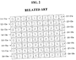
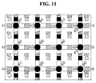
- FIG. 1 is a plane view of a related art touch sensor integrated type display device
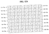
- FIG. 2 is a plane view showing a touch sensing location obtained by the touch sensor integrated type display device shown in FIG. 1 .
- the related art touch sensor integrated type display device includes an active area AA, in which touch/common electrodes T11-T1a, T21-T2a, T31-T3a, T41-T4a, T51-T5a, T61-T6a, T71-T7a, and T81-T8a are disposed and data is displayed, and a bezel area BA positioned outside the active area AA.
- a bezel area BA In the bezel area BA, various wires and a source and touch driving integrated circuit (IC) 10 are disposed.
- the active area AA includes the plurality of touch/common electrodes T11-T1a, T21-T2a, T31-T3a, T41-T4a, T51-T5a, T61-T6a, T71-T7a, and T81-T8a divided in a first direction (for example, x-axis direction) and a second direction (for example, y-axis direction) crossing the first direction and a plurality of touch/common routing wires W11-W81, W12-W82, W13-W83, W14-W84, W15-W85, W16-W86, W17-W87, W18-W88, W19-W89, and W1a-W8a, which are respectively connected to the plurality of touch/common electrodes T11-T1a, T21-T2a, T31-T3a, T41-T4a, T51-T5a, T61-T6a, T71-T7a, and T81-T
- the plurality of touch/common electrodes T11-T1a, T21-T2a, T31-T3a, T41-T4a, T51-T5a, T61-T6a, T71-T7a, and T81-T8a in the active area AA are formed by dividing a common electrode of the display device, and thus operate as common electrodes in a display driving mode for displaying data and operate as touch electrodes in a touch driving mode for recognizing a touch location.
- the bezel area BA positioned outside the active area AA includes the source and touch driving IC 10 and various wires.
- the source and touch driving IC 10 supplies display data to data lines (not shown) in synchronization with a drive of gate lines (not shown) of the display device and supplies a common voltage to the touch/common electrodes (or the common electrodes).
- the source and touch driving IC 10 supplies a touch driving voltage to the touch/common electrodes and scans a change in a capacitance of each touch/common electrode before and after a touch operation, thereby calculating a touch location, at which the touch operation is performed.
- the various wires include the touch/common routing wires W11-W81, W12-W82, W13-W83, W14-W84, W15-W85, W16-W86, W17-W87, W18-W88, W19-W89, and W1a-W8a connected to the touch/common electrodes T11-T1a, T21-T2a, T31-T3a, T41-T4a, T51-T5a, T61-T6a, T71-T7a, and T81-T8a, the gate lines connected to the source and touch driving IC 10, the data lines, and the like.
- the touch/common electrodes T11-T1a, T21-T2a, T31-T3a, T41-T4a, T51-T5a, T61-T6a, T71-T7a, and T81-T8a respectively have touch sensing nodes S11-S1a, S21-S2a, S31-S3a, S41-S4a, S51-S5a, S61-S6a, S71-S7a, and S81-S8a, which are recognized as the touch location when the touch operation is performed.
- the above-described related art touch sensor integrated type display device is configured so that the size of one touch/common electrode corresponds to the size of dozens of pixel electrodes and the touch/common electrodes are respectively connected to the touch/common routing wires.
- the number of touch/common electrodes is obtained by multiplying the number of touch/common electrodes positioned on one row and the number of touch/common electrodes positioned on one column. With a recent trend toward the large-sized display device, the display device becomes larger and larger and thus the number of touch/common electrodes sharply increases.
- the number of touch/common routing wires connected to the touch/common electrodes positioned on one column becomes more than the number of pixel electrodes positioned on one row in an area corresponding to each touch/common electrode. Hence, the touch/common routing wire not overlapping the data line is generated and thus reduces an aperture ratio of the display device.
- the touch/common routing wire is not connected to some of the touch/common electrodes so as to prevent the reduction of the aperture ratio, a touch location cannot be accurately recognized when the touch operation is performed on the touch/common electrode, to which the touch/common routing wire is not connected.
- the size of the display device to which the related art touch sensor integrated type display device can be applied.
- the number of channels of the source and touch driving IC 10 connected to the touch/common electrodes increases due to an increase in the number of touch/common routing wires, and thus the size of the readout integrated circuit increases. Hence, the manufacturing cost of the display device increases.
- Embodiments of the invention provide a touch sensor integrated type display device capable of solving the above-described problems.
- a touch sensor integrated type display device comprising a display panel, a data driving circuit, a scan driving circuit, a multiplexer, a readout integrated circuit (IC), and a touch controller.
- the display panel includes data lines and gate lines crossing over each other, a plurality of touch/common electrodes divided and arranged in directions crossing over each other, and a plurality of touch/common routing wires respectively connected to the plurality of touch/common electrodes and is time-division driven in a display driving period and a touch driving period.
- the data driving circuit supplies video data voltages to the data lines during the display driving period.
- the scan driving circuit sequentially supplies scan pulses synchronized with the video data voltages to the gate lines during the display driving period.
- the multiplexing unit supplies a common voltage to the plurality of touch/common electrodes during the display driving period, supplies a touch driving voltage to the plurality of touch/common electrodes several times during the touch driving period, and senses the plurality of touch/common electrodes several times using a self-capacitive method and a mutual capacitive method.
- the readout IC receives sensing voltages sensed from the plurality of touch/common electrodes via the multiplexing unit during the touch driving period.
- the touch controller supplies a plurality of switching control signals to the multiplexing unit and calculates a touch location based on the sensing voltages received from the readout IC.
- the touch sensor integrated type display device further comprises a switching block, an integrating block, and a timing controller.
- the switching block is connected to the multiplexing unit and performs a switching operation for supplying the common voltage to the plurality of touch/common electrodes during the display driving period, and supplying the touch driving voltage to the plurality of touch/common electrodes during the touch driving period, and outputting the sensing voltages.
- the integrating block integrates the sensing voltages supplied from the switching block during the touch driving period and outputs the integrated sensing voltages to the readout IC.
- the timing controller generates timing control signals for controlling operation timings of the data driving circuit and the scan driving circuit and a touch/display control signal for controlling the switching block.
- the multiplexing unit includes a first multiplexer having input terminals connected to the plurality of touch/common electrodes.
- the switching block includes a plurality of switching units selectively connected to output terminals of the first multiplexer.
- the integrating block includes a plurality of integrators respectively connected to the plurality of switching units.
- the first multiplexer supplies the touch driving voltage supplied through the plurality of switching units to the plurality of touch/common electrodes during the touch driving period and outputs first sensing voltages obtained by sensing each of the plurality of touch/common electrodes.
- the first multiplexer includes a plurality of 1-1 switching elements respectively connected to the plurality of touch/common electrodes and configured to perform a switching operation in response to a 1-1 switching control signal supplied from the touch controller, a plurality of 1-2 switching elements respectively connected to the plurality of touch/common electrodes and configured to perform a switching operation in response to a 1-2 switching control signal supplied from the touch controller, a plurality of 1-3 switching elements respectively connected to the plurality of touch/common electrodes and configured to perform a switching operation in response to a 1-3 switching control signal supplied from the touch controller, and a plurality of 1-4 switching elements respectively connected to the plurality of touch/common electrodes and configured to perform a switching operation in response to a 1-4 switching control signal supplied from the touch controller.
- the multiplexing unit includes a second multiplexer having input terminals connected to the plurality of touch/common electrodes and output terminals selectively connected to the plurality of integrators.
- the second multiplexer during the touch driving period, supplies the touch driving voltage supplied through the plurality of switching units to touch/common electrodes positioned in one of first and second columns adjacent to each other in a horizontal direction, and outputs second sensing voltages obtained by sensing the touch/common electrodes positioned in another one of the first and second columns.
- the second multiplexer includes a plurality of 2-1 switching elements respectively connected to the plurality of touch/common electrodes and configured to perform a switching operation in response to a 2-1 switching control signal supplied from the touch controller, a plurality of 2-2 switching elements respectively connected to the plurality of touch/common electrodes and configured to perform a switching operation in response to a 2-2 switching control signal supplied from the touch controller, and a plurality of 2-3 switching elements respectively connected to the plurality of touch/common electrodes and configured to perform a switching operation in response to a 2-3 switching control signal supplied from the touch controller.
- the multiplexing unit includes a third multiplexer having input terminals connected to the plurality of touch/common electrodes and output terminals selectively connected to the plurality of integrators.
- the third multiplexer during the touch driving period, supplies the touch driving voltage supplied through the plurality of switching units to touch/common electrodes positioned in one of first and second rows adjacent to each other in a vertical direction, and outputs third sensing voltages obtained by sensing touch/common electrodes positioned in another one of the first and second rows.
- the third multiplexer includes a plurality of 3-1 switching elements respectively connected to the plurality of touch/common electrodes and configured to perform a switching operation in response to a 3-1 switching control signal supplied from the touch controller, a plurality of 3-2 switching elements respectively connected to the plurality of touch/common electrodes and configured to perform a switching operation in response to a 3-2 switching control signal supplied from the touch controller, a plurality of 3-3 switching elements respectively connected to the plurality of touch/common electrodes and configured to perform a switching operation in response to a 3-3 switching control signal supplied from the touch controller, and a plurality of 3-4 switching elements respectively connected to the plurality of touch/common electrodes and configured to perform a switching operation in response to a 3-4 switching control signal supplied from the touch controller.
- the multiplexing unit includes a fourth multiplexer having input terminals connected to the plurality of touch/common electrodes and output terminals selectively connected to the plurality of integrators.
- the fourth multiplexer during the touch driving period, supplies the touch driving voltage supplied through the plurality of switching units to the touch/common electrodes positioned in one of first and second diagonals adjacent to each other in a diagonal direction and outputs fourth sensing voltages obtained by sensing the touch/common electrodes positioned in another one of first and second diagonals.
- the fourth multiplexer includes a plurality of 4-1 switching elements respectively connected to the plurality of touch/common electrodes and configured to perform a switching operation in response to a 4-1 switching control signal supplied from the touch controller, a plurality of 4-2 switching elements respectively connected to the plurality of touch/common electrodes and configured to perform a switching operation in response to a 4-2 switching control signal supplied from the touch controller, a plurality of 4-3 switching elements respectively connected to the plurality of touch/common electrodes and configured to perform a switching operation in response to a 4-3 switching control signal supplied from the touch controller, and a plurality of 4-4 switching elements respectively connected to the plurality of touch/common electrodes and configured to perform a switching operation in response to a 4-4 switching control signal supplied from the touch controller.
- the plurality of integrators integrate the first to fourth sensing voltages and output the integrated first to fourth sensing voltages to the readout IC.
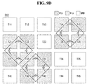
- sizes of the touch/common electrodes positioned at each side of the display panel among the plurality of touch/common electrodes are smaller than sizes of the remaining touch/common electrodes.
- each of the plurality of touch/common electrodes includes a stem, at least one branch extended from the stem and at least one concave formed towards inside of the stem.
- the at least one branch is disposed in the at least one concave of a touch/common electrode adjacent thereto.
- the at least one branch has one shape of a bar shape, a sawtooth, a T character and a reverse T character.
- the plurality of touch/common electrodes have the same size.
- sizes of the touch/common electrodes positioned at each side of the display panel among the plurality of touch/common electrodes are smaller than sizes of the remaining touch/common electrodes.
- the invention can be applied to large-screen display devices and also can reduce the number of touch channels of the readout IC, thereby reducing the manufacturing cost.
- the invention can obtain a touch resolution at the same level as the related art through a self-capacitive method and a plurality of mutual capacitive methods.
- each touch/common electrode lengths of sides of each touch/common electrode are increased by coupling construction in which the first and second branches Tb1 and Tb2 are disposed in the first and concaves Tc1 and Tc2 in touch/common electrodes adjacent to each other. Accordingly, it is possible to obtain an improved touch resolution because the mutual capacitance between the adjacent touch/common electrodes is increased.
- a touch sensor integrated type display device may be implemented as in-cell type touch sensors embedded in a flat panel display, such as a liquid crystal display (LCD), a field emission display (FED), a plasma display panel (PDP), an organic light emitting diode display, and an electrophoresis display (EPD).
- a flat panel display such as a liquid crystal display (LCD), a field emission display (FED), a plasma display panel (PDP), an organic light emitting diode display, and an electrophoresis display (EPD).
- LCD liquid crystal display
- FED field emission display
- PDP plasma display panel
- EPD electrophoresis display
- FIG. 3 is a block diagram schematically showing the touch sensor integrated type display device according to the embodiment of the invention.
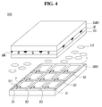
- FIG. 4 is a partial exploded perspective view schematically showing a partial area of the touch sensor integrated type display device according to the embodiment of the invention.
- the touch sensor integrated type display device includes a display panel 100, a data driving circuit 202, a scan driving circuit 204, a timing controller 104, a multiplexer MUX (herein also referred to as multiplexing unit), a switching block SB, an integrating block IB, a readout integrated circuit (IC) ROIC, a touch controller TC, and the like.
- a display panel 100 a data driving circuit 202, a scan driving circuit 204, a timing controller 104, a multiplexer MUX (herein also referred to as multiplexing unit), a switching block SB, an integrating block IB, a readout integrated circuit (IC) ROIC, a touch controller TC, and the like.
- the display panel 100 includes a lower glass substrate SUB1, an upper glass substrate SUB2, and a liquid crystal layer disposed between the lower glass substrate SUB1 and the upper glass substrate SUB2.
- a pixel array is disposed on the lower glass substrate SUB1 of the display panel 100.
- the pixel array includes a plurality of data lines D1 to Dm, where m is a positive integer, a plurality of gate lines (or scan lines) G1 to Gn crossing the data lines D1 to Dm, where n is a positive integer, a plurality of thin film transistors (TFTs) disposed at crossings of the data lines D1 to Dm and the gate lines G1 to Gn, a plurality of pixel electrodes P for charging liquid crystal cells Clc to a data voltage, a plurality of storage capacitors Cst which are connected to the pixel electrodes P and maintain a voltage of the liquid crystal cells Clc, and touch/common electrodes T.
- TFTs thin film transistors
- Pixels of the display panel 100 are respectively disposed in pixel areas defined by the data lines D1 to Dm and the gate lines G1 to Gn to form a matrix structure.
- the liquid crystal cell Clc of each pixel is driven by an electric field generated depending on a voltage difference between the data voltage supplied to the pixel electrode P and a common voltage Vcom supplied to the touch/common electrode T, thereby adjusting an amount of incident light transmitted by the liquid crystal cell.
- the TFTs are turned on in response to a gate pulse (or a scan pulse) from the gate lines G1 to Gn and supply the voltage from the data lines D1 to Dm to the pixel electrodes P of the liquid crystal cells Clc.
- the upper glass substrate SUB2 of the display panel 100 may include black matrixes BM, red (R), green (G), and blue (B) color filters CF, an overcoat layer OC covering the black matrixes BM and the R, G, and B color filters CF, and the like.
- the lower glass substrate SUB1 of the display panel 100 may be configured as a color filter on TFT (COT) structure.
- the black matrixes BM and the color filters CF may be disposed on the lower glass substrate SUB1 of the display panel 100.
- the touch/common electrodes T are disposed on the upper glass substrate SUB2 in a vertical electric field driving manner, such as a twisted nematic (TN) mode and a vertical alignment (VA) mode. Further, the touch/common electrodes T are disposed on the lower glass substrate SUB1 along with the pixel electrodes P in a horizontal electric field driving manner, such as an in-plane switching (IPS) mode and a fringe field switching (FFS) mode.
- IPS in-plane switching
- FFS fringe field switching
- the touch/common electrodes T are connected to touch/common routing wires W11 to W45 and receive the common voltage Vcom.
- Polarizing plates are respectively attached to the upper and lower glass substrates SUB2 and SUB1 of the display panel 100.
- Alignment layers for setting a pre-tilt angle of liquid crystals are respectively disposed on the inner surfaces contacting the liquid crystals in the upper and lower glass substrates SUB2 and SUB1 of the display panel 100.
- a column spacer may be disposed between the upper and lower glass substrates SUB2 and SUB1 of the display panel 100 to keep cell gaps of the liquid crystal cells Clc constant.
- the data driving circuit 202 includes a plurality of source driving integrated circuits (ICs).
- the source driving ICs output an analog video data voltage during a previously set display driving period.
- the source driving ICs latch digital video data RGB received from the timing controller 104.
- the source driving ICs convert the digital video data RGB into positive and negative analog gamma compensation voltages and output the analog video data voltage.
- the analog video data voltage is supplied to the data lines D1 to Dm.
- the scan driving circuit 204 includes at least one scan driving IC.
- the scan driving IC sequentially supplies the scan pulse synchronized with the analog video data voltage to the gate lines G1 to Gn under the control of the timing controller 104 during the display driving period and selects lines of the display panel 100, to which the analog video data voltage is applied.
- the scan pulse is generated as a pulse swinging between a gate high voltage and a gate low voltage.
- the scan driving circuit 204 does not generate the scan pulse during a touch driving period and continuously supplies the gate low voltage to the gate lines G1 to Gn during the touch driving period.
- the scan driving IC supplies the gate pulse to the TFTs of the pixels through the gate lines G1 to Gn and sequentially selects lines of the display panel 100, to which data will be applied.
- the scan driving IC is maintained at the gate low voltage.
- the timing controller 104 receives timing signals, such as a vertical sync signal Vsync, a horizontal sync signal Hsync, a data enable signal DE, and a main clock MCLK, from an external host system.
- the timing controller 104 generates timing control signals for controlling operation timings of the data driving circuit 202 and the scan driving circuit 204 and generates a touch/display control signal Ctd for controlling the switching block SB based on the timing signals.
- the timing control signal of the scan driving circuit 204 includes a gate start pulse GSP, a gate shift clock GSC, a gate output enable signal GOE, a shift direction control signal DIR, and the like.
- the timing control signal of the data driving circuit 202 includes a source sampling clock SSC, a source output enable signal SOE, a polarity control signal POL, and the like.
- the timing controller 104 controls the timing control signals and time-divides one frame period into at least one display driving period and at least one touch driving period.
- the timing controller 104 enables an output of the data driving circuit 202 and an output of the scan driving circuit 204 and displays video data on the pixels.
- the timing controller 104 drives the touch controller TC and detects a touch location of a touch screen.
- the display driving period and the touch driving period may be properly adjusted depending on kinds of display panels in consideration of their panel characteristics.
- the multiplexer MUX supplies a touch driving voltage to the touch/common electrodes T in response to the touch/display control signal Ctd and senses the touch/common electrodes T using a self-capacitive method and a mutual capacitive method to output sensing voltages.
- the integrating block IB integrates the sensing voltages received from the multiplexer MUX and outputs the integrated sensing voltages.
- the readout IC ROIC converts the integrated sensing voltages received from the integrating block IB into digital data of a human interface device (HID) format and outputs the digital data.
- HID human interface device
- the touch controller TC supplies switching control signals C11 to C44 controlling the multiplexer MUX to the multiplexer MUX.
- the touch controller TC analyzes the digital data received from the readout IC ROIC using a previously set touch recognition algorithm and calculates coordinate values. Coordinate data of a touch location output from the touch controller TC is transmitted to the external host system (not shown). The host system runs an application program the coordinate data of the touch location indicates.
- FIG. 5 is a block diagram schematically showing a basic configuration for touch recognition in the touch sensor integrated type display device according to the embodiment of the invention.
- the touch sensor integrated type display device includes a plurality of touch/common electrodes T11-T15, T21-T25, T31-T35, and T41-T45 disposed in a display area of the display panel 100, a plurality of touch/common routing wires W11-W41, W12-W42, W13-W43, W14-W44, and W15-W45 respectively connected to the plurality of touch/common electrodes T11-T15, T21-T25, T31-T35, and T41-T45, the multiplexer MUX, the integrating block IB, the readout IC ROIC, and the touch controller TC.
- the plurality of touch/common electrodes T11-T15, T21-T25, T31-T35, and T41-T45 are divided and arranged in a first direction (for example, x-axis direction) and a second direction (for example, y-axis direction) crossing the first direction.
- the plurality of touch/common routing wires W11-W41, W12-W42, W13-W43, W14-W44, and W15-W45 are respectively connected to the plurality of touch/common electrodes T11-T15, T21-T25, T31-T35, and T41-T45 and are arranged in the second direction.
- the multiplexer MUX includes a first multiplexer MUX-S for sensing the plurality of touch/common electrodes T11-T15, T21-T25, T31-T35, and T41-T45 using the self-capacitive method, a second multiplexer MUX-M1 for sensing the plurality of touch/common electrodes T11-T15, T21-T25, T31-T35, and T41-T45 using a first mutual capacitive method of a horizontal direction, a third multiplexer MUX-M2 for sensing the plurality of touch/common electrodes T11-T15, T21-T25, T31-T35, and T41-T45 using a second mutual capacitive method of a vertical direction, and a fourth multiplexer MUX-M3 for sensing the plurality of touch/common electrodes T11-T15, T21-T25, T31-T35, and T41-T45 using a third mutual capacitive method of
- the integrating block IB includes first to fifth integrators I1 to I5.
- the integrating block IB integrates the sensing voltages output from the first to fourth multiplexers MUX-S and MUX-M1 to MUX-M3 of the multiplexer MUX and outputs the integrated sensing voltages.
- the readout IC ROIC converts the integrated sensing voltages received from the integrating block IB into digital data of the HID format and outputs the digital data.
- the touch controller TC analyzes the digital data received from the readout IC ROIC using a previously set touch recognition algorithm and calculates coordinate values of touch locations.
- the coordinate data of the touch locations output from the touch controller TC are transmitted to the external host system.
- the host system runs an application program to which the coordinate data of the touch locations indicates.
- the touch recognition method of the touch sensor integrated type display device includes a self-capacitive sensing step (refer to FIGS. 6A to 6C ) of sensing each of the touch/common electrodes using the self-capacitive method, a first mutual capacitive sensing step (refer to FIGS. 7A to 7E ) of sensing the touch/common electrodes in a horizontal direction using a mutual capacitive method, a second mutual capacitive sensing step (refer to FIGS. 8A to 8E ) of sensing the touch/common electrodes in a vertical direction using the mutual capacitive method, and a third mutual capacitive sensing step (refer to FIGS.
- the embodiment of the invention describes that the self-capacitive sensing step and the first to third mutual capacitive sensing steps are sequentially performed. However, order of the above four sensing steps may be variously changed.
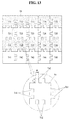
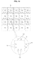
- FIG. 6A is a circuit diagram illustrating a step of sensing each touch/common electrode using a self-capacitive method in the touch sensor integrated type display device according to the embodiment of the invention.
- FIG. 6B is a plane view showing the touch/common electrodes sensed using the self-capacitive method shown in FIG. 6A .
- FIG. 6C is a plane view showing sensing locations of the touch/common electrodes sensed using the self-capacitive method shown in FIG. 6A .
- the touch sensor integrated type display device for the self-capacitive sensing includes the first multiplexer MUX-S of the multiplexer MUX and the switching block SB, which is disposed between the first multiplexer MUX-S and the integrating block IB, supplies the common voltage Vcom during a display driving period, and supplies a touch driving voltage Vtx during a touch driving period.
- the first multiplexer MUX-S includes 1-1 to 4-20 switching elements Sa01-Sa20, Sb01-Sb20, Sc01-Sc20, and Sd01-Sd20.
- the 1-1 switching element Sa01 includes a first terminal connected to the 1-1 touch/common routing wire W11 connected to the 1-1 touch/common electrode T11, a second terminal connected to a first input terminal 'a' of the first integrator I1, and a control terminal receiving a 1-1 switching control signal C11 supplied from the touch controller TC.
- the 1-2 switching element Sa02 includes a first terminal connected to the 2-1 touch/common routing wire W21 connected to the 2-1 touch/common electrode T21, a second terminal connected to a ground terminal GND, and a control terminal receiving the 1-1 switching control signal C11 supplied from the touch controller TC.
- the 1-3 switching element Sa03 includes a first terminal connected to the 3-1 touch/common routing wire W31 connected to the 3-1 touch/common electrode T31, a second terminal connected to the ground terminal GND, and a control terminal receiving the 1-1 switching control signal C11 supplied from the touch controller TC.
- the 1-4 switching element Sa04 includes a first terminal connected to the 4-1 touch/common routing wire W41 connected to the 4-1 touch/common electrode T41, a second terminal connected to the ground terminal GND, and a control terminal receiving the 1-1 switching control signal C11 supplied from the touch controller TC.
- the 1-5 switching element Sa05 includes a first terminal connected to the 1-2 touch/common routing wire W12 connected to the 1-2 touch/common electrode T12, a second terminal connected to a first input terminal 'a' of the second integrator I2, and a control terminal receiving the 1-1 switching control signal C11 supplied from the touch controller TC.
- the 1-6 switching element Sa06 includes a first terminal connected to the 2-2 touch/common routing wire W22 connected to the 2-2 touch/common electrode T22, a second terminal connected to the ground terminal GND, and a control terminal receiving the 1-1 switching control signal C11 supplied from the touch controller TC.
- the 1-7 switching element Sa07 includes a first terminal connected to the 3-2 touch/common routing wire W32 connected to the 3-2 touch/common electrode T32, a second terminal connected to the ground terminal GND, and a control terminal receiving the 1-1 switching control signal C11 supplied from the touch controller TC.
- the 1-8 switching element Sa08 includes a first terminal connected to the 4-2 touch/common routing wire W42 connected to the 4-2 touch/common electrode T42, a second terminal connected to the ground terminal GND, and a control terminal receiving the 1-1 switching control signal C11 supplied from the touch controller TC.
- the 1-9 switching element Sa09 includes a first terminal connected to the 1-3 touch/common routing wire W13 connected to the 1-3 touch/common electrode T13, a second terminal connected to a first input terminal 'a' of the third integrator I3, and a control terminal receiving the 1-1 switching control signal C11 supplied from the touch controller TC.
- the 1-10 switching element Sa10 includes a first terminal connected to the 2-3 touch/common routing wire W23 connected to the 2-3 touch/common electrode T23, a second terminal connected to the ground terminal GND, and a control terminal receiving the 1-1 switching control signal C11 supplied from the touch controller TC.
- the 1-11 switching element Sa11 includes a first terminal connected to the 3-3 touch/common routing wire W33 connected to the 3-3 touch/common electrode T33, a second terminal connected to the ground terminal GND, and a control terminal receiving the 1-1 switching control signal C11 supplied from the touch controller TC.
- the 1-12 switching element Sa12 includes a first terminal connected to the 4-3 touch/common routing wire W43 connected to the 4-3 touch/common electrode T43, a second terminal connected to the ground terminal GND, and a control terminal receiving the 1-1 switching control signal C11 supplied from the touch controller TC.
- the 1-13 switching element Sa13 includes a first terminal connected to the 1-4 touch/common routing wire W14 connected to the 1-4 touch/common electrode T14, a second terminal connected to a first input terminal 'a' of the fourth integrator I4, and a control terminal receiving the 1-1 switching control signal C11 supplied from the touch controller TC.
- the 1-14 switching element Sa14 includes a first terminal connected to the 2-4 touch/common routing wire W24 connected to the 2-4 touch/common electrode T24, a second terminal connected to the ground terminal GND, and a control terminal receiving the 1-1 switching control signal C11 supplied from the touch controller TC.
- the 1-15 switching element Sa15 includes a first terminal connected to the 3-4 touch/common routing wire W34 connected to the 3-4 touch/common electrode T34, a second terminal connected to the ground terminal GND, and a control terminal receiving the 1-1 switching control signal C11 supplied from the touch controller TC.
- the 1-16 switching element Sa16 includes a first terminal connected to the 4-4 touch/common routing wire W44 connected to the 4-4 touch/common electrode T44, a second terminal connected to the ground terminal GND, and a control terminal receiving the 1-1 switching control signal C11 supplied from the touch controller TC.
- the 1-17 switching element Sa17 includes a first terminal connected to the 1-5 touch/common routing wire W15 connected to the 1-5 touch/common electrode T15, a second terminal connected to a first input terminal 'a' of the fifth integrator I5, and a control terminal receiving the 1-1 switching control signal C11 supplied from the touch controller TC.
- the 1-18 switching element Sa18 includes a first terminal connected to the 2-5 touch/common routing wire W25 connected to the 2-5 touch/common electrode T25, a second terminal connected to the ground terminal GND, and a control terminal receiving the 1-1 switching control signal C11 supplied from the touch controller TC.
- the 1-19 switching element Sa19 includes a first terminal connected to the 3-5 touch/common routing wire W35 connected to the 3-5 touch/common electrode T35, a second terminal connected to the ground terminal GND, and a control terminal receiving the 1-1 switching control signal C11 supplied from the touch controller TC.
- the 1-20 switching element Sa20 includes a first terminal connected to the 4-5 touch/common routing wire W45 connected to the 4-5 touch/common electrode T45, a second terminal connected to the ground terminal GND, and a control terminal receiving the 1-1 switching control signal C11 supplied from the touch controller TC.
- the 2-1 switching element Sb01 includes a first terminal connected to the 1-1 touch/common routing wire W11 connected to the 1-1 touch/common electrode T11, a second terminal connected to the ground terminal GND, and a control terminal receiving a 1-2 switching control signal C12 supplied from the touch controller TC.
- the 2-2 switching element Sb02 includes a first terminal connected to the 2-1 touch/common routing wire W21 connected to the 2-1 touch/common electrode T21, a second terminal connected to the first input terminal 'a' of the first integrator I1, and a control terminal receiving the 1-2 switching control signal C12 supplied from the touch controller TC.
- the 2-3 switching element Sb03 includes a first terminal connected to the 3-1 touch/common routing wire W31 connected to the 3-1 touch/common electrode T31, a second terminal connected to the ground terminal GND, and a control terminal receiving the 1-2 switching control signal C12 supplied from the touch controller TC.
- the 2-4 switching element Sb04 includes a first terminal connected to the 4-1 touch/common routing wire W41 connected to the 4-1 touch/common electrode T41, a second terminal connected to the ground terminal GND, and a control terminal receiving the 1-2 switching control signal C12 supplied from the touch controller TC.
- the 2-5 switching element Sb05 includes a first terminal connected to the 1-2 touch/common routing wire W12 connected to the 1-2 touch/common electrode T12, a second terminal connected to the ground terminal GND, and a control terminal receiving the 1-2 switching control signal C12 supplied from the touch controller TC.
- the 2-6 switching element Sb06 includes a first terminal connected to the 2-2 touch/common routing wire W22 connected to the 2-2 touch/common electrode T22, a second terminal connected to the first input terminal 'a' of the second integrator I2, and a control terminal receiving the 1-2 switching control signal C12 supplied from the touch controller TC.
- the 2-7 switching element Sb07 includes a first terminal connected to the 3-2 touch/common routing wire W32 connected to the 3-2 touch/common electrode T32, a second terminal connected to the ground terminal GND, and a control terminal receiving the 1-2 switching control signal C12 supplied from the touch controller TC.
- the 2-8 switching element Sb08 includes a first terminal connected to the 4-2 touch/common routing wire W42 connected to the 4-2 touch/common electrode T42, a second terminal connected to the ground terminal GND, and a control terminal receiving the 1-2 switching control signal C12 supplied from the touch controller TC.
- the 2-9 switching element Sb09 includes a first terminal connected to the 1-3 touch/common routing wire W13 connected to the 1-3 touch/common electrode T13, a second terminal connected to the ground terminal GND, and a control terminal receiving the 1-2 switching control signal C12 supplied from the touch controller TC.
- the 2-10 switching element Sb10 includes a first terminal connected to the 2-3 touch/common routing wire W23 connected to the 2-3 touch/common electrode T23, a second terminal connected to the first input terminal 'a' of the third integrator I3, and a control terminal receiving the 1-2 switching control signal C12 supplied from the touch controller TC.
- the 2-11 switching element Sb11 includes a first terminal connected to the 3-3 touch/common routing wire W33 connected to the 3-3 touch/common electrode T33, a second terminal connected to the ground terminal GND, and a control terminal receiving the 1-2 switching control signal C12 supplied from the touch controller TC.
- the 2-12 switching element Sb12 includes a first terminal connected to the 4-3 touch/common routing wire W43 connected to the 4-3 touch/common electrode T43, a second terminal connected to the ground terminal GND, and a control terminal receiving the 1-2 switching control signal C12 supplied from the touch controller TC.
- the 2-13 switching element Sb13 includes a first terminal connected to the 1-4 touch/common routing wire W14 connected to the 1-4 touch/common electrode T14, a second terminal connected to the ground terminal GND, and a control terminal receiving the 1-2 switching control signal C12 supplied from the touch controller TC.
- the 2-14 switching element Sb14 includes a first terminal connected to the 2-4 touch/common routing wire W24 connected to the 2-4 touch/common electrode T24, a second terminal connected to the first input terminal 'a' of the fourth integrator I4, and a control terminal receiving the 1-2 switching control signal C12 supplied from the touch controller TC.
- the 2-15 switching element Sb15 includes a first terminal connected to the 3-4 touch/common routing wire W34 connected to the 3-4 touch/common electrode T34, a second terminal connected to the ground terminal GND, and a control terminal receiving the 1-2 switching control signal C12 supplied from the touch controller TC.
- the 2-16 switching element Sb16 includes a first terminal connected to the 4-4 touch/common routing wire W44 connected to the 4-4 touch/common electrode T44, a second terminal connected to the ground terminal GND, and a control terminal receiving the 1-2 switching control signal C12 supplied from the touch controller TC.
- the 2-17 switching element Sb17 includes a first terminal connected to the 1-5 touch/common routing wire W15 connected to the 1-5 touch/common electrode T15, a second terminal connected to the ground terminal GND, and a control terminal receiving the 1-2 switching control signal C12 supplied from the touch controller TC.
- the 2-18 switching element Sb18 includes a first terminal connected to the 2-5 touch/common routing wire W25 connected to the 2-5 touch/common electrode T25, a second terminal connected to the first input terminal 'a' of the fifth integrator I5, and a control terminal receiving the 1-2 switching control signal C12 supplied from the touch controller TC.
- the 2-19 switching element Sb19 includes a first terminal connected to the 3-5 touch/common routing wire W35 connected to the 3-5 touch/common electrode T35, a second terminal connected to the ground terminal GND, and a control terminal receiving the 1-2 switching control signal C12 supplied from the touch controller TC.
- the 2-20 switching element Sb20 includes a first terminal connected to the 4-5 touch/common routing wire W45 connected to the 4-5 touch/common electrode T45, a second terminal connected to the ground terminal GND, and a control terminal receiving the 1-2 switching control signal C12 supplied from the touch controller TC.
- the 3-1 switching element Sc01 includes a first terminal connected to the 1-1 touch/common routing wire W11 connected to the 1-1 touch/common electrode T11, a second terminal connected to the ground terminal GND, and a control terminal receiving a 1-3 switching control signal C13 supplied from the touch controller TC.
- the 3-2 switching element Sc02 includes a first terminal connected to the 2-1 touch/common routing wire W21 connected to the 2-1 touch/common electrode T21, a second terminal connected to the ground terminal GND, and a control terminal receiving the 1-3 switching control signal C13 supplied from the touch controller TC.
- the 3-3 switching element Sc03 includes a first terminal connected to the 3-1 touch/common routing wire W31 connected to the 3-1 touch/common electrode T31, a second terminal connected to the first input terminal 'a' of the first integrator I1, and a control terminal receiving the 1-3 switching control signal C13 supplied from the touch controller TC.
- the 3-4 switching element Sc04 includes a first terminal connected to the 4-1 touch/common routing wire W41 connected to the 4-1 touch/common electrode T41, a second terminal connected to the ground terminal GND, and a control terminal receiving the 1-3 switching control signal C13 supplied from the touch controller TC.
- the 3-5 switching element Sc05 includes a first terminal connected to the 1-2 touch/common routing wire W12 connected to the 1-2 touch/common electrode T12, a second terminal connected to the ground terminal GND, and a control terminal receiving the 1-3 switching control signal C13 supplied from the touch controller TC.
- the 3-6 switching element Sc06 includes a first terminal connected to the 2-2 touch/common routing wire W22 connected to the 2-2 touch/common electrode T22, a second terminal connected to the ground terminal GND, and a control terminal receiving the 1-3 switching control signal C13 supplied from the touch controller TC.
- the 3-7 switching element Sc07 includes a first terminal connected to the 3-2 touch/common routing wire W32 connected to the 3-2 touch/common electrode T32, a second terminal connected to the first input terminal 'a' of the second integrator I2, and a control terminal receiving the 1-3 switching control signal C13 supplied from the touch controller TC.
- the 3-8 switching element Sc08 includes a first terminal connected to the 4-2 touch/common routing wire W42 connected to the 4-2 touch/common electrode T42, a second terminal connected to the ground terminal GND, and a control terminal receiving the 1-3 switching control signal C13 supplied from the touch controller TC.
- the 3-9 switching element Sc09 includes a first terminal connected to the 1-3 touch/common routing wire W13 connected to the 1-3 touch/common electrode T13, a second terminal connected to the ground terminal GND, and a control terminal receiving the 1-3 switching control signal C13 supplied from the touch controller TC.
- the 3-10 switching element Sc10 includes a first terminal connected to the 2-3 touch/common routing wire W23 connected to the 2-3 touch/common electrode T23, a second terminal connected to the ground terminal GND, and a control terminal receiving the 1-3 switching control signal C13 supplied from the touch controller TC.
- the 3-11 switching element Sc11 includes a first terminal connected to the 3-3 touch/common routing wire W33 connected to the 3-3 touch/common electrode T33, a second terminal connected to the first input terminal 'a' of the third integrator I3, and a control terminal receiving the 1-3 switching control signal C13 supplied from the touch controller TC.
- the 3-12 switching element Sc12 includes a first terminal connected to the 4-3 touch/common routing wire W43 connected to the 4-3 touch/common electrode T43, a second terminal connected to the ground terminal GND, and a control terminal receiving the 1-3 switching control signal C13 supplied from the touch controller TC.
- the 3-13 switching element Sc13 includes a first terminal connected to the 1-4 touch/common routing wire W14 connected to the 1-4 touch/common electrode T14, a second terminal connected to the ground terminal GND, and a control terminal receiving the 1-3 switching control signal C13 supplied from the touch controller TC.
- the 3-14 switching element Sc14 includes a first terminal connected to the 2-4 touch/common routing wire W24 connected to the 2-4 touch/common electrode T24, a second terminal connected to the ground terminal GND, and a control terminal receiving the 1-3 switching control signal C13 supplied from the touch controller TC.
- the 3-15 switching element Sc15 includes a first terminal connected to the 3-4 touch/common routing wire W34 connected to the 3-4 touch/common electrode T34, a second terminal connected to the first input terminal 'a' of the fourth integrator I4, and a control terminal receiving the 1-3 switching control signal C13 supplied from the touch controller TC.
- the 3-16 switching element Sc16 includes a first terminal connected to the 4-4 touch/common routing wire W44 connected to the 4-4 touch/common electrode T44, a second terminal connected to the ground terminal GND, and a control terminal receiving the 1-3 switching control signal C13 supplied from the touch controller TC.
- the 3-17 switching element Sc17 includes a first terminal connected to the 1-5 touch/common routing wire W15 connected to the 1-5 touch/common electrode T15, a second terminal connected to the ground terminal GND, and a control terminal receiving the 1-3 switching control signal C13 supplied from the touch controller TC.
- the 3-18 switching element Sc18 includes a first terminal connected to the 2-5 touch/common routing wire W25 connected to the 2-5 touch/common electrode T25, a second terminal connected to the ground terminal GND, and a control terminal receiving the 1-3 switching control signal C13 supplied from the touch controller TC.
- the 3-19 switching element Sc19 includes a first terminal connected to the 3-5 touch/common routing wire W35 connected to the 3-5 touch/common electrode T35, a second terminal connected to the first input terminal 'a' of the fifth integrator I5, and a control terminal receiving the 1-3 switching control signal C13 supplied from the touch controller TC.
- the 3-20 switching element Sc20 includes a first terminal connected to the 4-5 touch/common routing wire W45 connected to the 4-5 touch/common electrode T45, a second terminal connected to the ground terminal GND, and a control terminal receiving the 1-3 switching control signal C13 supplied from the touch controller TC.
- the 4-1 switching element Sd01 includes a first terminal connected to the 1-1 touch/common routing wire W11 connected to the 1-1 touch/common electrode T11, a second terminal connected to the ground terminal GND, and a control terminal receiving a 1-4 switching control signal C14 supplied from the touch controller TC.
- the 4-2 switching element Sd02 includes a first terminal connected to the 2-1 touch/common routing wire W21 connected to the 2-1 touch/common electrode T21, a second terminal connected to the ground terminal GND, and a control terminal receiving the 1-4 switching control signal C14 supplied from the touch controller TC.
- the 4-3 switching element Sd03 includes a first terminal connected to the 3-1 touch/common routing wire W31 connected to the 3-1 touch/common electrode T31, a second terminal connected to the ground terminal GND, and a control terminal receiving the 1-4 switching control signal C14 supplied from the touch controller TC.
- the 4-4 switching element Sd04 includes a first terminal connected to the 4-1 touch/common routing wire W41 connected to the 4-1 touch/common electrode T41, a second terminal connected to the first input terminal 'a' of the first integrator I1, and a control terminal receiving the 1-4 switching control signal C14 supplied from the touch controller TC.
- the 4-5 switching element Sd05 includes a first terminal connected to the 1-2 touch/common routing wire W12 connected to the 1-2 touch/common electrode T12, a second terminal connected to the ground terminal GND, and a control terminal receiving the 1-4 switching control signal C14 supplied from the touch controller TC.
- the 4-6 switching element Sd06 includes a first terminal connected to the 2-2 touch/common routing wire W22 connected to the 2-2 touch/common electrode T22, a second terminal connected to the ground terminal GND, and a control terminal receiving the 1-4 switching control signal C14 supplied from the touch controller TC.
- the 4-7 switching element Sd07 includes a first terminal connected to the 3-2 touch/common routing wire W32 connected to the 3-2 touch/common electrode T32, a second terminal connected to the ground terminal GND, and a control terminal receiving the 1-4 switching control signal C14 supplied from the touch controller TC.
- the 4-8 switching element Sd08 includes a first terminal connected to the 4-2 touch/common routing wire W42 connected to the 4-2 touch/common electrode T42, a second terminal connected to the first input terminal 'a' of the second integrator I2, and a control terminal receiving the 1-4 switching control signal C14 supplied from the touch controller TC.
- the 4-9 switching element Sd09 includes a first terminal connected to the 1-3 touch/common routing wire W13 connected to the 1-3 touch/common electrode T13, a second terminal connected to the ground terminal GND, and a control terminal receiving the 1-4 switching control signal C14 supplied from the touch controller TC.
- the 4-10 switching element Sd10 includes a first terminal connected to the 2-3 touch/common routing wire W23 connected to the 2-3 touch/common electrode T23, a second terminal connected to the ground terminal GND, and a control terminal receiving the 1-4 switching control signal C14 supplied from the touch controller TC.
- the 4-11 switching element Sd11 includes a first terminal connected to the 3-3 touch/common routing wire W33 connected to the 3-3 touch/common electrode T33, a second terminal connected to the ground terminal GND, and a control terminal receiving the 1-4 switching control signal C14 supplied from the touch controller TC.
- the 4-12 switching element Sd12 includes a first terminal connected to the 4-3 touch/common routing wire W43 connected to the 4-3 touch/common electrode T43, a second terminal connected to the first input terminal 'a' of the third integrator I3, and a control terminal receiving the 1-4 switching control signal C14 supplied from the touch controller TC.
- the 4-13 switching element Sd13 includes a first terminal connected to the 1-4 touch/common routing wire W14 connected to the 1-4 touch/common electrode T14, a second terminal connected to the ground terminal GND, and a control terminal receiving the 1-4 switching control signal C14 supplied from the touch controller TC.
- the 4-14 switching element Sd14 includes a first terminal connected to the 2-4 touch/common routing wire W24 connected to the 2-4 touch/common electrode T24, a second terminal connected to the ground terminal GND, and a control terminal receiving the 1-4 switching control signal C14 supplied from the touch controller TC.
- the 4-15 switching element Sd15 includes a first terminal connected to the 3-4 touch/common routing wire W34 connected to the 3-4 touch/common electrode T34, a second terminal connected to the ground terminal GND, and a control terminal receiving the 1-4 switching control signal C14 supplied from the touch controller TC.
- the 4-16 switching element Sd16 includes a first terminal connected to the 4-4 touch/common routing wire W44 connected to the 4-4 touch/common electrode T44, a second terminal connected to the first input terminal 'a' of the fourth integrator I4, and a control terminal receiving the 1-4 switching control signal C14 supplied from the touch controller TC.
- the 4-17 switching element Sd17 includes a first terminal connected to the 1-5 touch/common routing wire W15 connected to the 1-5 touch/common electrode T15, a second terminal connected to the ground terminal GND, and a control terminal receiving the 1-4 switching control signal C14 supplied from the touch controller TC.
- the 4-18 switching element Sd18 includes a first terminal connected to the 2-5 touch/common routing wire W25 connected to the 2-5 touch/common electrode T25, a second terminal connected to the ground terminal GND, and a control terminal receiving the 1-4 switching control signal C14 supplied from the touch controller TC.
- the 4-19 switching element Sd19 includes a first terminal connected to the 3-5 touch/common routing wire W35 connected to the 3-5 touch/common electrode T35, a second terminal connected to the ground terminal GND, and a control terminal receiving the 1-4 switching control signal C14 supplied from the touch controller TC.
- the 4-20 switching element Sd20 includes a first terminal connected to the 4-5 touch/common routing wire W45 connected to the 4-5 touch/common electrode T45, a second terminal connected to the first input terminal 'a' of the fifth integrator I5, and a control terminal receiving the 1-4 switching control signal C14 supplied from the touch controller TC.
- the 1-1 to 4-20 switching elements Sa01-Sa20, Sb01-Sb20, Sc01-Sc20, and Sd01-Sd20 may be implemented as switching thin film transistors.
- the switching block SB is disposed between the first multiplexer MUX-S and the integrating block IB and includes first to fifth switching units SW1 to SW5.
- the first switching unit SW1 includes a 1-1 terminal n11 connected to the second terminals of the 1-1, 2-2, 3-3, and 4-4 switching elements Sa01, Sb02, Sc03, and Sd04, a 1-2 terminal n12 connected to the first input terminal 'a' of the first integrator I1, and a 1-3 terminal n13 to which the common voltage Vcom is applied.
- the first switching unit SW1 supplies the common voltage Vcom to the first multiplexer MUX-S in response to the touch/display control signal Ctd supplied from the timing controller 104 in a display driving mode and supplies the touch driving voltage Vtx to the first multiplexer MUX-S in response to the touch/display control signal Ctd in a touch sensor drive.
- the second switching unit SW2 includes a 2-1 terminal n21 connected to the second terminals of the 1-5, 2-6, 3-7, and 4-8 switching elements Sa05, Sb06, Sc07, and Sd08, a 2-2 terminal n22 connected to the first input terminal 'a' of the second integrator I2, and a 2-3 terminal n23 to which the common voltage Vcom is applied.
- the second switching unit SW2 supplies the common voltage Vcom to the first multiplexer MUX-S in response to the touch/display control signal Ctd supplied from the timing controller 104 in the display driving mode and supplies the touch driving voltage Vtx to the first multiplexer MUX-S in response to the touch/display control signal Ctd in the touch sensor drive.
- the third switching unit SW3 includes a 3-1 terminal n31 connected to the second terminals of the 1-9, 2-10, 3-11, and 4-12 switching elements Sa09, Sb10, Sc11, and Sd12, a 3-2 terminal n32 connected to the first input terminal 'a' of the third integrator I3, and a 3-3 terminal n33 to which the common voltage Vcom is applied.
- the third switching unit SW3 supplies the common voltage Vcom to the first multiplexer MUX-S in response to the touch/display control signal Ctd supplied from the timing controller 104 in the display driving mode and supplies the touch driving voltage Vtx to the first multiplexer MUX-S in response to the touch/display control signal Ctd in the touch sensor drive.
- the fourth switching unit SW4 includes a 4-1 terminal n41 connected to the second terminals of the 1-13, 2-14, 3-15, and 4-16 switching elements Sa13, Sb14, Sc15, and Sd16, a 4-2 terminal n42 connected to the first input terminal 'a' of the fourth integrator I4, and a 4-3 terminal n43 to which the common voltage Vcom is applied.
- the fourth switching unit SW4 supplies the common voltage Vcom to the first multiplexer MUX-S in response to the touch/display control signal Ctd supplied from the timing controller 104 in the display driving mode and supplies the touch driving voltage Vtx to the first multiplexer MUX-S in response to the touch/display control signal Ctd in the touch sensor drive.
- the fifth switching unit SW5 includes a 5-1 terminal n51 connected to the second terminals of the 1-17, 2-18, 3-19, and 4-20 switching elements Sa17, Sb18, Sc19, and Sd20, a 5-2 terminal n52 connected to the first input terminal 'a' of the fifth integrator I5, and a 5-3 terminal n53 to which the common voltage Vcom is applied.
- the fifth switching unit SW5 supplies the common voltage Vcom to the first multiplexer MUX-S in response to the touch/display control signal Ctd supplied from the timing controller 104 in the display driving mode and supplies the touch driving voltage Vtx to the first multiplexer MUX-S in response to the touch/display control signal Ctd in the touch sensor drive.
- Each of the first to fifth switching units SW1 to SW5 may be configured as an n-metal-oxide-semiconductor (MOS) transistor and a p-MOS transistor. When the switching units SW1 to SW5 are configured as described above, the two transistors may reversely operate in response to one control signal. Each of the first to fifth switching units SW1 to SW5 may be configured using two same transistors. In this instance, signals supplied to the two transistors have to be reversed.
- MOS n-metal-oxide-semiconductor
- the first to fifth switching units SW1 to SW5 connect a common voltage supply source and the first multiplexer MUX-S in response to the touch/display control signal Ctd.
- the 1-1 to 4-20 switching elements Sa01-Sa20, Sb01-Sb20, Sc01-Sc20, and Sd01-Sd20 of the first multiplexer MUX-S are turned on in response to the 1-1 to 1-4 switching control signals C11 to C14 supplied from the touch controller TC.
- the common voltage Vcom is supplied to all of the touch/common electrodes T11-T15, T21-T25, T31-T35, and T41-T45 through the touch/common routing wires W11-W41, W12-W42, W13-W43, W14-W44, and W15-W45, and data is displayed on the display screen.
- the first to fifth switching units SW1 to SW5 connect the integrating block IB and the first multiplexer MUX-S in response to the touch/display control signal Ctd.
- the touch controller TC sequentially supplies the 1-1 to 1-4 switching control signals C11 to C14 to the first multiplexer MUX-S.
- the touch controller TC supplies the 1-1 switching control signal C11 to the first multiplexer MUX-S of the multiplexer MUX
- the 1-1 switching control signal C11 is supplied to the control terminals of the 1-1 to 1-20 switching elements Sa01 to Sa20 of the first multiplexer MUX-S and turns on the 1-1 to 1-20 switching elements Sa01 to Sa20.
- the touch driving voltage Vtx is supplied to the 1-1 to 1-5 touch/common electrodes T11 to T15 of a first row through the first to fifth switching units SW1 to SW5 and the 1-1 to 1-20 switching elements Sa01 to Sa20, and at the same time the 1-1 to 1-5 touch/common electrodes T11 to T15 are sensed.
- the 1-1 to 1-5 sensing voltages are supplied to the first input terminals 'a' of the first to fifth integrators I1 to I5 through the 1-1 to 1-20 switching elements Sa01 to Sa20 and the first to fifth switching units SW1 to SW5.
- the first to fifth integrators I1 to I5 perform the supply and the sensing of the touch driving voltage Vtx several times and integrate the 1-1 to 1-5 sensing voltages.
- the integrated 1-1 to 1-5 sensing voltages are output to the readout IC ROIC.
- the readout IC ROIC converts the integrated 1-1 to 1-5 sensing voltages into digital data of the HID format and outputs the digital data.
- the touch controller TC analyzes the digital data received from the readout IC ROIC using a previously set touch recognition algorithm and calculates coordinate values. Hence, the embodiment of the invention can distinguish where a touch operation is performed at sensing locations SW11 to SW15 of the 1-1 to 1-5 touch/common electrodes T11 to T15 of the first row shown in FIGS. 6B and 6C .
- the touch controller TC supplies the 1-2 switching control signal C12 to the first multiplexer MUX-S of the multiplexer MUX
- the 1-2 switching control signal C12 is supplied to the control terminals of the 2-1 to 2-20 switching elements Sb01 to Sb20 of the first multiplexer MUX-S and turns on the 2-1 to 2-20 switching elements Sb01 to Sb20.
- the touch driving voltage Vtx is supplied to the 2-1 to 2-5 touch/common electrodes T21 to T25 of a second row through the first to fifth switching units SW1 to SW5 and the 2-1 to 2-20 switching elements Sb01 to Sb20, and at the same time the 2-1 to 2-5 touch/common electrodes T21 to T25 are sensed.
- the 2-1 to 2-5 sensing voltages are supplied to the first input terminals 'a' of the first to fifth integrators I1 to I5 through the 2-1 to 2-20 switching elements Sb01 to Sb20 and the first to fifth switching units SW1 to SW5.
- the first to fifth integrators I1 to I5 perform the supply and the sensing of the touch driving voltage Vtx several times and integrate the 2-1 to 2-5 sensing voltages.
- the integrated 2-1 to 2-5 sensing voltages are output to the readout IC ROIC.
- the readout IC ROIC converts the integrated 2-1 to 2-5 sensing voltages into digital data of the HID format and outputs the digital data.
- the touch controller TC analyzes the digital data received from the readout IC ROIC using the previously set touch recognition algorithm and calculates coordinate values. Hence, the embodiment of the invention can distinguish where a touch operation is performed at sensing locations SW21 to SW25 of the 2-1 to 2-5 touch/common electrodes T21 to T25 of the second row shown in FIGS. 6B and 6C .
- the touch controller TC supplies the 1-3 switching control signal C13 to the first multiplexer MUX-S of the multiplexer MUX
- the 1-3 switching control signal C13 is supplied to the control terminals of the 3-1 to 3-20 switching elements Sc01 to Sc20 of the first multiplexer MUX-S and turns on the 3-1 to 3-20 switching elements Sc01 to Sc20.
- the touch driving voltage Vtx is supplied to the 3-1 to 3-5 touch/common electrodes T31 to T35 of a third row through the first to fifth switching units SW1 to SW5 and the 3-1 to 3-20 switching elements Sc01 to Sc20, and at the same time the 3-1 to 3-5 touch/common electrodes T31 to T35 are sensed.
- the 3-1 to 3-5 sensing voltages are supplied to the first input terminals 'a' of the first to fifth integrators I1 to I5 through the 3-1 to 3-20 switching elements Sc01 to Sc20 and the first to fifth switching units SW1 to SW5.
- the first to fifth integrators I1 to I5 perform the supply and the sensing of the touch driving voltage Vtx several times and integrate the 3-1 to 3-5 sensing voltages.
- the integrated 3-1 to 3-5 sensing voltages are output to the readout IC ROIC.
- the readout IC ROIC converts the integrated 3-1 to 3-5 sensing voltages into digital data of the HID format and outputs the digital data.
- the touch controller TC analyzes the digital data received from the readout IC ROIC using the previously set touch recognition algorithm and calculates coordinate values. Hence, the embodiment of the invention can distinguish where a touch operation is performed at sensing locations SW31 to SW35 of the 3-1 to 3-5 touch/common electrodes T31 to T35 of the third row shown in FIGS. 6B and 6C .
- the touch controller TC supplies the 1-4 switching control signal C14 to the first multiplexer MUX-S of the multiplexer MUX
- the 1-4 switching control signal C14 is supplied to the control terminals of the 4-1 to 4-20 switching elements Sd01 to Sd20 of the first multiplexer MUX-S and turns on the 4-1 to 4-20 switching elements Sd01 to Sd20.
- the touch driving voltage Vtx is supplied to the 4-1 to 4-5 touch/common electrodes T41 to T45 of a fourth row through the first to fifth switching units SW1 to SW5 and the 4-1 to 4-20 switching elements Sd01 to Sd20, and at the same time the 4-1 to 4-5 touch/common electrodes T41 to T45 are sensed.
- the 4-1 to 4-5 sensing voltages are supplied to the first input terminals 'a' of the first to fifth integrators I1 to I5 through the 4-1 to 4-20 switching elements Sd01 to Sd20 and the first to fifth switching units SW1 to SW5.
- the first to fifth integrators I1 to I5 perform the supply and the sensing of the touch driving voltage Vtx several times and integrate the 4-1 to 4-5 sensing voltages.
- the integrated 4-1 to 4-5 sensing voltages are output to the readout IC ROIC.
- the readout IC ROIC converts the integrated 4-1 to 4-5 sensing voltages into digital data of the HID format and outputs the digital data.
- the touch controller TC analyzes the digital data received from the readout IC ROIC using the previously set touch recognition algorithm and calculates coordinate values. Hence, the embodiment of the invention can distinguish where a touch operation is performed at sensing locations SW41 to SW45 of the 4-1 to 4-5 touch/common electrodes T41 to T45 of the fourth row shown in FIGS. 6B and 6C .
- the embodiment of the invention can distinguish where the touch operation is performed at the sensing locations SW11-SW15, SW21-SW25, SW31-SW35, and SW41 ⁇ SW45 of the touch/common electrodes T11-T15, T21-T25, T31-T35, and T41-T45 through the above-described touch sensing step.
- the sensing locations capable of being obtained through the self-capacitive sensing step are shown in FIG. 6C .
- the first mutual capacitive sensing is performed.
- FIG. 7A is a circuit diagram showing a configuration for sensing the touch/common electrodes through a first mutual capacitive method after the self-capacitive sensing in the touch sensor integrated type display device according to the embodiment of the invention.
- FIG. 7B is a plane view illustrating a step for sensing the touch/common electrodes through a 1-1 mutual capacitive method using the circuit diagram shown in FIG. 7A .
- FIG. 7C is a plane view additionally showing sensing locations capable of being sensed through the 1-1 mutual capacitive method shown in FIG. 7B .
- FIG. 7A is a circuit diagram showing a configuration for sensing the touch/common electrodes through a first mutual capacitive method after the self-capacitive sensing in the touch sensor integrated type display device according to the embodiment of the invention.
- FIG. 7B is a plane view illustrating a step for sensing the touch/common electrodes through a 1-1 mutual capacitive method using the circuit diagram shown in FIG. 7A .
- FIG. 7D is a plane view illustrating a step for sensing the touch/common electrodes through a 1-2 mutual capacitive method using the circuit diagram shown in FIG. 7A .
- FIG. 7E is a plane view additionally showing sensing locations capable of being sensed through the 1-2 mutual capacitive method shown in FIG. 7D .
- the touch sensor integrated type display device for the first mutual capacitive sensing includes the second multiplexer MUX-M1 of the multiplexer MUX.
- the second multiplexer MUX-M1 includes m1-1 to m3-20 switching elements mSa01-mSa20, mSb01-mSb20, and mSc1-mSc20.
- the m1-1 switching element mSa01 includes a first terminal connected to the 1-1 touch/common routing wire W11 connected to the 1-1 touch/common electrode T11, a second terminal connected to a touch driving voltage source Vtx, and a control terminal receiving a 2-1 switching control signal C21 supplied from the touch controller TC.
- the m1-2 switching element mSa02 includes a first terminal connected to the 2-1 touch/common routing wire W21 connected to the 2-1 touch/common electrode T21, a second terminal connected to the first input terminal 'a' of the first integrator I1, and a control terminal receiving the 2-1 switching control signal C21 supplied from the touch controller TC.
- the m1-3 switching element mSa03 includes a first terminal connected to the 3-1 touch/common routing wire W31 connected to the 3-1 touch/common electrode T31, a second terminal connected to the ground terminal GND, and a control terminal receiving the 2-1 switching control signal C21 supplied from the touch controller TC.
- the m1-4 switching element mSa04 includes a first terminal connected to the 4-1 touch/common routing wire W41 connected to the 4-1 touch/common electrode T41, a second terminal connected to the ground terminal GND, and a control terminal receiving the 2-1 switching control signal C21 supplied from the touch controller TC.
- the m1-5 switching element mSa05 includes a first terminal connected to the 1-2 touch/common routing wire W12 connected to the 1-2 touch/common electrode T12, a second terminal connected to the touch driving voltage source Vtx, and a control terminal receiving the 2-1 switching control signal C21 supplied from the touch controller TC.
- the m1-6 switching element mSa06 includes a first terminal connected to the 2-2 touch/common routing wire W22 connected to the 2-2 touch/common electrode T22, a second terminal connected to the first input terminal 'a' of the second integrator I2, and a control terminal receiving the 2-1 switching control signal C21 supplied from the touch controller TC.
- the m1-7 switching element mSa07 includes a first terminal connected to the 3-2 touch/common routing wire W32 connected to the 3-2 touch/common electrode T32, a second terminal connected to the ground terminal GND, and a control terminal receiving the 2-1 switching control signal C21 supplied from the touch controller TC.
- the m1-8 switching element mSa08 includes a first terminal connected to the 4-2 touch/common routing wire W42 connected to the 4-2 touch/common electrode T42, a second terminal connected to the ground terminal GND, and a control terminal receiving the 2-1 switching control signal C21 supplied from the touch controller TC.
- the m1-9 switching element mSa09 includes a first terminal connected to the 1-3 touch/common routing wire W13 connected to the 1-3 touch/common electrode T13, a second terminal connected to the touch driving voltage source Vtx, and a control terminal receiving the 2-1 switching control signal C21 supplied from the touch controller TC.
- the m1-10 switching element mSa10 includes a first terminal connected to the 2-3 touch/common routing wire W23 connected to the 2-3 touch/common electrode T23, a second terminal connected to the first input terminal 'a' of the third integrator I3, and a control terminal receiving the 2-1 switching control signal C21 supplied from the touch controller TC.
- the m1-11 switching element mSa11 includes a first terminal connected to the 3-3 touch/common routing wire W33 connected to the 3-3 touch/common electrode T33, a second terminal connected to the ground terminal GND, and a control terminal receiving the 2-1 switching control signal C21 supplied from the touch controller TC.
- the m1-12 switching element mSa12 includes a first terminal connected to the 4-3 touch/common routing wire W43 connected to the 4-3 touch/common electrode T43, a second terminal connected to the ground terminal GND, and a control terminal receiving the 2-1 switching control signal C21 supplied from the touch controller TC.
- the m1-13 switching element mSa13 includes a first terminal connected to the 1-4 touch/common routing wire W14 connected to the 1-4 touch/common electrode T14, a second terminal connected to the touch driving voltage source Vtx, and a control terminal receiving the 2-1 switching control signal C21 supplied from the touch controller TC.
- the m1-14 switching element mSa14 includes a first terminal connected to the 2-4 touch/common routing wire W24 connected to the 2-4 touch/common electrode T24, a second terminal connected to the first input terminal 'a' of the fourth integrator I4, and a control terminal receiving the 2-1 switching control signal C21 supplied from the touch controller TC.
- the m1-15 switching element mSa15 includes a first terminal connected to the 3-4 touch/common routing wire W34 connected to the 3-4 touch/common electrode T34, a second terminal connected to the ground terminal GND, and a control terminal receiving the 2-1 switching control signal C21 supplied from the touch controller TC.
- the m1-16 switching element mSa16 includes a first terminal connected to the 4-4 touch/common routing wire W44 connected to the 4-4 touch/common electrode T44, a second terminal connected to the ground terminal GND, and a control terminal receiving the 2-1 switching control signal C21 supplied from the touch controller TC.
- the m1-17 switching element mSa17 includes a first terminal connected to the 1-5 touch/common routing wire W15 connected to the 1-5 touch/common electrode T15, a second terminal connected to the touch driving voltage source Vtx, and a control terminal receiving the 2-1 switching control signal C21 supplied from the touch controller TC.
- the m1-18 switching element mSa18 includes a first terminal connected to the 2-5 touch/common routing wire W25 connected to the 2-5 touch/common electrode T25, a second terminal connected to the first input terminal 'a' of the fifth integrator I5, and a control terminal receiving the 2-1 switching control signal C21 supplied from the touch controller TC.
- the m1-19 switching element mSa19 includes a first terminal connected to the 3-5 touch/common routing wire W35 connected to the 3-5 touch/common electrode T35, a second terminal connected to the ground terminal GND, and a control terminal receiving the 2-1 switching control signal C21 supplied from the touch controller TC.
- the m1-20 switching element mSa20 includes a first terminal connected to the 4-5 touch/common routing wire W45 connected to the 4-5 touch/common electrode T45, a second terminal connected to the ground terminal GND, and a control terminal receiving the 2-1 switching control signal C21 supplied from the touch controller TC.
- the m2-1 switching element mSb01 includes a first terminal connected to the 1-1 touch/common routing wire W11 connected to the 1-1 touch/common electrode T11, a second terminal connected to the ground terminal GND, and a control terminal receiving a 2-2 switching control signal C22 supplied from the touch controller TC.
- the m2-2 switching element mSb02 includes a first terminal connected to the 2-1 touch/common routing wire W21 connected to the 2-1 touch/common electrode T21, a second terminal connected to the first input terminal 'a' of the first integrator I1, and a control terminal receiving the 2-2 switching control signal C22 supplied from the touch controller TC.
- the m2-3 switching element mSb03 includes a first terminal connected to the 3-1 touch/common routing wire W31 connected to the 3-1 touch/common electrode T31, a second terminal connected to the touch driving voltage source Vtx, and a control terminal receiving the 2-2 switching control signal C22 supplied from the touch controller TC.
- the m2-4 switching element mSb04 includes a first terminal connected to the 4-1 touch/common routing wire W41 connected to the 4-1 touch/common electrode T41, a second terminal connected to the ground terminal GND, and a control terminal receiving the 2-2 switching control signal C22 supplied from the touch controller TC.
- the m2-5 switching element mSb05 includes a first terminal connected to the 1-2 touch/common routing wire W12 connected to the 1-2 touch/common electrode T12, a second terminal connected to the ground terminal GND, and a control terminal receiving the 2-2 switching control signal C22 supplied from the touch controller TC.
- the m2-6 switching element mSb06 includes a first terminal connected to the 2-2 touch/common routing wire W22 connected to the 2-2 touch/common electrode T22, a second terminal connected to the first input terminal 'a' of the second integrator I2, and a control terminal receiving the 2-2 switching control signal C22 supplied from the touch controller TC.
- the m2-7 switching element mSb07 includes a first terminal connected to the 3-2 touch/common routing wire W32 connected to the 3-2 touch/common electrode T32, a second terminal connected to the touch driving voltage source Vtx, and a control terminal receiving the 2-2 switching control signal C22 supplied from the touch controller TC.
- the m2-8 switching element mSb08 includes a first terminal connected to the 4-2 touch/common routing wire W42 connected to the 4-2 touch/common electrode T42, a second terminal connected to the ground terminal GND, and a control terminal receiving the 2-2 switching control signal C22 supplied from the touch controller TC.
- the m2-9 switching element mSb09 includes a first terminal connected to the 1-3 touch/common routing wire W13 connected to the 1-3 touch/common electrode T13, a second terminal connected to the ground terminal GND, and a control terminal receiving the 2-2 switching control signal C22 supplied from the touch controller TC.
- the m2-10 switching element mSb10 includes a first terminal connected to the 2-3 touch/common routing wire W23 connected to the 2-3 touch/common electrode T23, a second terminal connected to the first input terminal 'a' of the third integrator I3, and a control terminal receiving the 2-2 switching control signal C22 supplied from the touch controller TC.
- the m2-11 switching element mSb11 includes a first terminal connected to the 3-3 touch/common routing wire W33 connected to the 3-3 touch/common electrode T33, a second terminal connected to the touch driving voltage source Vtx, and a control terminal receiving the 2-2 switching control signal C22 supplied from the touch controller TC.
- the m2-12 switching element mSb12 includes a first terminal connected to the 4-3 touch/common routing wire W43 connected to the 4-3 touch/common electrode T43, a second terminal connected to the ground terminal GND, and a control terminal receiving the 2-2 switching control signal C22 supplied from the touch controller TC.
- the m2-13 switching element mSb13 includes a first terminal connected to the 1-4 touch/common routing wire W14 connected to the 1-4 touch/common electrode T14, a second terminal connected to the ground terminal GND, and a control terminal receiving the 2-2 switching control signal C22 supplied from the touch controller TC.
- the m2-14 switching element mSb14 includes a first terminal connected to the 2-4 touch/common routing wire W24 connected to the 2-4 touch/common electrode T24, a second terminal connected to the first input terminal 'a' of the fourth integrator I4, and a control terminal receiving the 2-2 switching control signal C22 supplied from the touch controller TC.
- the m2-15 switching element mSb15 includes a first terminal connected to the 3-4 touch/common routing wire W34 connected to the 3-4 touch/common electrode T34, a second terminal connected to the touch driving voltage source Vtx, and a control terminal receiving the 2-2 switching control signal C22 supplied from the touch controller TC.
- the m2-16 switching element mSb16 includes a first terminal connected to the 4-4 touch/common routing wire W44 connected to the 4-4 touch/common electrode T44, a second terminal connected to the ground terminal GND, and a control terminal receiving the 2-2 switching control signal C22 supplied from the touch controller TC.
- the m2-17 switching element mSb17 includes a first terminal connected to the 1-5 touch/common routing wire W15 connected to the 1-5 touch/common electrode T15, a second terminal connected to the ground terminal GND, and a control terminal receiving the 2-2 switching control signal C22 supplied from the touch controller TC.
- the m2-18 switching element mSb18 includes a first terminal connected to the 2-5 touch/common routing wire W25 connected to the 2-5 touch/common electrode T25, a second terminal connected to the first input terminal 'a' of the fifth integrator I5, and a control terminal receiving the 2-2 switching control signal C22 supplied from the touch controller TC.
- the m2-19 switching element mSb19 includes a first terminal connected to the 3-5 touch/common routing wire W35 connected to the 3-5 touch/common electrode T35, a second terminal connected to the touch driving voltage source Vtx, and a control terminal receiving the 2-2 switching control signal C22 supplied from the touch controller TC.
- the m2-20 switching element mSb20 includes a first terminal connected to the 4-5 touch/common routing wire W45 connected to the 4-5 touch/common electrode T45, a second terminal connected to the ground terminal GND, and a control terminal receiving the 2-2 switching control signal C22 supplied from the touch controller TC.
- the m3-1 switching element mSc01 includes a first terminal connected to the 1-1 touch/common routing wire W11 connected to the 1-1 touch/common electrode T11, a second terminal connected to the ground terminal GND, and a control terminal receiving a 2-3 switching control signal C23 supplied from the touch controller TC.
- the m3-2 switching element mSc02 includes a first terminal connected to the 2-1 touch/common routing wire W21 connected to the 2-1 touch/common electrode T21, a second terminal connected to the ground terminal GND, and a control terminal receiving the 2-3 switching control signal C23 supplied from the touch controller TC.
- the m3-3 switching element mSc03 includes a first terminal connected to the 3-1 touch/common routing wire W31 connected to the 3-1 touch/common electrode T31, a second terminal connected to the touch driving voltage source Vtx, and a control terminal receiving the 2-3 switching control signal C23 supplied from the touch controller TC.
- the m3-4 switching element mSc04 includes a first terminal connected to the 4-1 touch/common routing wire W41 connected to the 4-1 touch/common electrode T41, a second terminal connected to the first input terminal 'a' of the first integrator I1, and a control terminal receiving the 2-3 switching control signal C23 supplied from the touch controller TC.
- the m3-5 switching element mSc05 includes a first terminal connected to the 1-2 touch/common routing wire W12 connected to the 1-2 touch/common electrode T12, a second terminal connected to the ground terminal GND, and a control terminal receiving the 2-3 switching control signal C23 supplied from the touch controller TC.
- the m3-6 switching element mSc06 includes a first terminal connected to the 2-2 touch/common routing wire W22 connected to the 2-2 touch/common electrode T22, a second terminal connected to the ground terminal GND, and a control terminal receiving the 2-3 switching control signal C23 supplied from the touch controller TC.
- the m3-7 switching element mSc07 includes a first terminal connected to the 3-2 touch/common routing wire W32 connected to the 3-2 touch/common electrode T32, a second terminal connected to the touch driving voltage source Vtx, and a control terminal receiving the 2-3 switching control signal C23 supplied from the touch controller TC.
- the m3-8 switching element mSc08 includes a first terminal connected to the 4-2 touch/common routing wire W42 connected to the 4-2 touch/common electrode T42, a second terminal connected to the first input terminal 'a' of the second integrator I2, and a control terminal receiving the 2-3 switching control signal C23 supplied from the touch controller TC.
- the m3-9 switching element mSc09 includes a first terminal connected to the 1-3 touch/common routing wire W13 connected to the 1-3 touch/common electrode T13, a second terminal connected to the ground terminal GND, and a control terminal receiving the 2-3 switching control signal C23 supplied from the touch controller TC.
- the m3-10 switching element mSc10 includes a first terminal connected to the 2-3 touch/common routing wire W23 connected to the 2-3 touch/common electrode T23, a second terminal connected to the ground terminal GND, and a control terminal receiving the 2-3 switching control signal C23 supplied from the touch controller TC.
- the m3-11 switching element mSc11 includes a first terminal connected to the 3-3 touch/common routing wire W33 connected to the 3-3 touch/common electrode T33, a second terminal connected to the touch driving voltage source Vtx, and a control terminal receiving the 2-3 switching control signal C23 supplied from the touch controller TC.
- the m3-12 switching element mSc12 includes a first terminal connected to the 4-3 touch/common routing wire W43 connected to the 4-3 touch/common electrode T43, a second terminal connected to the first input terminal 'a' of the third integrator I3, and a control terminal receiving the 2-3 switching control signal C23 supplied from the touch controller TC.
- the m3-13 switching element mSc13 includes a first terminal connected to the 1-4 touch/common routing wire W14 connected to the 1-4 touch/common electrode T14, a second terminal connected to the ground terminal GND, and a control terminal receiving the 2-3 switching control signal C23 supplied from the touch controller TC.
- the m3-14 switching element mSc14 includes a first terminal connected to the 2-4 touch/common routing wire W24 connected to the 2-4 touch/common electrode T24, a second terminal connected to the ground terminal GND, and a control terminal receiving the 2-3 switching control signal C23 supplied from the touch controller TC.
- the m3-15 switching element mSc15 includes a first terminal connected to the 3-4 touch/common routing wire W34 connected to the 3-4 touch/common electrode T34, a second terminal connected to the touch driving voltage source Vtx, and a control terminal receiving the 2-3 switching control signal C23 supplied from the touch controller TC.
- the m3-16 switching element mSc16 includes a first terminal connected to the 4-4 touch/common routing wire W44 connected to the 4-4 touch/common electrode T44, a second terminal connected to the first input terminal 'a' of the fourth integrator I4, and a control terminal receiving the 2-3 switching control signal C23 supplied from the touch controller TC.
- the m3-17 switching element mSc17 includes a first terminal connected to the 1-5 touch/common routing wire W15 connected to the 1-5 touch/common electrode T15, a second terminal connected to the ground terminal GND, and a control terminal receiving the 2-3 switching control signal C23 supplied from the touch controller TC.
- the m3-18 switching element mSc18 includes a first terminal connected to the 2-5 touch/common routing wire W25 connected to the 2-5 touch/common electrode T25, a second terminal connected to the ground terminal GND, and a control terminal receiving the 2-3 switching control signal C23 supplied from the touch controller TC.
- the m3-19 switching element mSc19 includes a first terminal connected to the 3-5 touch/common routing wire W35 connected to the 3-5 touch/common electrode T35, a second terminal connected to the touch driving voltage source Vtx, and a control terminal receiving the 2-3 switching control signal C23 supplied from the touch controller TC.
- the m3-20 switching element mSc20 includes a first terminal connected to the 4-5 touch/common routing wire W45 connected to the 4-5 touch/common electrode T45, a second terminal connected to the first input terminal 'a' of the fifth integrator I5, and a control terminal receiving the 2-3 switching control signal C23 supplied from the touch controller TC.
- the m1-1 to m3-20 switching elements mSa01-mSa20, mSb01-mSb20, and mSc1-mSc20 may be implemented as switching thin film transistors.
- the touch controller TC supplies the 2-1 switching control signal C21 to the second multiplexer MUX-M1 of the multiplexer MUX
- the 2-1 switching control signal C21 is supplied to the control terminals of the m1-1 to m1-20 switching elements mSa01 to mSa20 of the second multiplexer MUX-M1 and turns on the m1-1 to m1-20 switching elements mSa01 to mSa20.
- the touch driving voltage Vtx is supplied to the 1-1 to 1-5 touch/common electrodes T11 to T15 of a first row.
- the 2-1 to 2-5 touch/common electrodes T21 to T25 of a second row are respectively connected to the first input terminals 'a' of the first to fifth integrators I1 to I5.
- sensing locations h1 to h15 of a first horizontal location may be obtained.
- the touch controller TC stops supplying the 2-1 switching control signal C21 and supplies the 2-2 switching control signal C22 to the second multiplexer MUX-M1 of the multiplexer MUX
- the 2-2 switching control signal C22 is supplied to the control terminals of the m2-1 to m2-20 switching elements mSb01 to mSb20 of the second multiplexer MUX-M1 and turns on the m2-1 to m2-20 switching elements mSb01 to mSb20.
- the touch driving voltage Vtx is supplied to the 3-1 to 3-5 touch/common electrodes T31 to T35 of a third row.
- the 2-1 to 2-5 touch/common electrodes T21 to T25 of the second row are respectively connected to the first input terminals 'a' of the first to fifth integrators I1 to I5.
- the touch controller TC stops supplying the 2-2 switching control signal C22 and supplies the 2-3 switching control signal C23 to the second multiplexer MUX-M1 of the multiplexer MUX
- the 2-3 switching control signal C23 is supplied to the control terminals of the m3-1 to m3-20 switching elements mSc01 to mSc20 of the second multiplexer MUX-M1 and turns on the m3-1 to m3-20 switching elements mSc01 to mSc20.
- the touch driving voltage Vtx is supplied to the 3-1 to 3-5 touch/common electrodes T31 to T35 of the third row.
- the 4-1 to 4-5 touch/common electrodes T41 to T45 of a fourth row are respectively connected to the first input terminals 'a' of the first to fifth integrators I1 to I5.
- the second mutual capacitive sensing is performed.
- FIG. 8A is a circuit diagram showing a configuration for sensing the touch/common electrodes through a second mutual capacitive method after the first mutual capacitive sensing in the touch sensor integrated type display device according to the embodiment of the invention.
- FIG. 8B is a plane view illustrating a step for sensing the touch/common electrodes through a 2-1 mutual capacitive method using the circuit diagram shown in FIG. 8A .
- FIG. 8C is a plane view additionally showing sensing locations capable of being sensed through the 2-1 mutual capacitive method shown in FIG. 8B .
- FIG. 8A is a circuit diagram showing a configuration for sensing the touch/common electrodes through a second mutual capacitive method after the first mutual capacitive sensing in the touch sensor integrated type display device according to the embodiment of the invention.
- FIG. 8B is a plane view illustrating a step for sensing the touch/common electrodes through a 2-1 mutual capacitive method using the circuit diagram shown in FIG. 8A .
- FIG. 8D is a plane view illustrating a step for sensing the touch/common electrodes through a 2-2 mutual capacitive method using the circuit diagram shown in FIG. 8A .
- FIG. 8E is a plane view additionally showing sensing locations capable of being sensed through the 2-2 mutual capacitive method shown in FIG. 8D .
- the touch sensor integrated type display device for the second mutual capacitive sensing includes the third multiplexer MUX-M2 of the multiplexer MUX.
- the third multiplexer MUX-M2 includes n1-1 to n4-20 switching elements nSa01-nSa20, nSb01-nSb20, nSc01-nSc20, and nSd01-nSd20.
- the n1-1 switching element nSa01 includes a first terminal connected to the 1-1 touch/common routing wire W11 connected to the 1-1 touch/common electrode T11, a second terminal connected to the touch driving voltage source Vtx, and a control terminal receiving a 3-1 switching control signal C31 supplied from the touch controller TC.
- the n1-2 switching element nSa02 includes a first terminal connected to the 2-1 touch/common routing wire W21 connected to the 2-1 touch/common electrode T21, a second terminal connected to the touch driving voltage source Vtx, and a control terminal receiving the 3-1 switching control signal C31 supplied from the touch controller TC.
- the n1-3 switching element nSa03 includes a first terminal connected to the 3-1 touch/common routing wire W31 connected to the 3-1 touch/common electrode T31, a second terminal connected to the touch driving voltage source Vtx, and a control terminal receiving the 3-1 switching control signal C31 supplied from the touch controller TC.
- the n1-4 switching element nSa04 includes a first terminal connected to the 4-1 touch/common routing wire W41 connected to the 4-1 touch/common electrode T41, a second terminal connected to the touch driving voltage source Vtx, and a control terminal receiving the 3-1 switching control signal C31 supplied from the touch controller TC.
- the n1-5 switching element nSa05 includes a first terminal connected to the 1-2 touch/common routing wire W12 connected to the 1-2 touch/common electrode T12, a second terminal connected to the first input terminal 'a' of the first integrator I1, and a control terminal receiving the 3-1 switching control signal C31 supplied from the touch controller TC.
- the n1-6 switching element nSa06 includes a first terminal connected to the 2-2 touch/common routing wire W22 connected to the 2-2 touch/common electrode T22, a second terminal connected to the first input terminal 'a' of the second integrator I2, and a control terminal receiving the 3-1 switching control signal C31 supplied from the touch controller TC.
- the n1-7 switching element nSa07 includes a first terminal connected to the 3-2 touch/common routing wire W32 connected to the 3-2 touch/common electrode T32, a second terminal connected to the first input terminal 'a' of the third integrator I3, and a control terminal receiving the 3-1 switching control signal C31 supplied from the touch controller TC.
- the n1-8 switching element nSa08 includes a first terminal connected to the 4-2 touch/common routing wire W42 connected to the 4-2 touch/common electrode T42, a second terminal connected to the first input terminal 'a' of the fourth integrator I4, and a control terminal receiving the 3-1 switching control signal C31 supplied from the touch controller TC.
- the n1-9 switching element nSa09 includes a first terminal connected to the 1-3 touch/common routing wire W13 connected to the 1-3 touch/common electrode T13, a second terminal connected to the ground terminal GND, and a control terminal receiving the 3-1 switching control signal C31 supplied from the touch controller TC.
- the n1-10 switching element nSa10 includes a first terminal connected to the 2-3 touch/common routing wire W23 connected to the 2-3 touch/common electrode T23, a second terminal connected to the ground terminal GND, and a control terminal receiving the 3-1 switching control signal C31 supplied from the touch controller TC.
- the n1-11 switching element nSa11 includes a first terminal connected to the 3-3 touch/common routing wire W33 connected to the 3-3 touch/common electrode T33, a second terminal connected to the ground terminal GND, and a control terminal receiving the 3-1 switching control signal C31 supplied from the touch controller TC.
- the n1-12 switching element nSa12 includes a first terminal connected to the 4-3 touch/common routing wire W43 connected to the 4-3 touch/common electrode T43, a second terminal connected to the ground terminal GND, and a control terminal receiving the 3-1 switching control signal C31 supplied from the touch controller TC.
- the n1-13 switching element nSa13 includes a first terminal connected to the 1-4 touch/common routing wire W14 connected to the 1-4 touch/common electrode T14, a second terminal connected to the ground terminal GND, and a control terminal receiving the 3-1 switching control signal C31 supplied from the touch controller TC.
- the n1-14 switching element nSa14 includes a first terminal connected to the 2-4 touch/common routing wire W24 connected to the 2-4 touch/common electrode T24, a second terminal connected to the ground terminal GND, and a control terminal receiving the 3-1 switching control signal C31 supplied from the touch controller TC.
- the n1-15 switching element nSa15 includes a first terminal connected to the 3-4 touch/common routing wire W34 connected to the 3-4 touch/common electrode T34, a second terminal connected to the ground terminal GND, and a control terminal receiving the 3-1 switching control signal C31 supplied from the touch controller TC.
- the n1-16 switching element nSa16 includes a first terminal connected to the 4-4 touch/common routing wire W44 connected to the 4-4 touch/common electrode T44, a second terminal connected to the ground terminal GND, and a control terminal receiving the 3-1 switching control signal C31 supplied from the touch controller TC.
- the n1-17 switching element nSa17 includes a first terminal connected to the 1-5 touch/common routing wire W15 connected to the 1-5 touch/common electrode T15, a second terminal connected to the ground terminal GND, and a control terminal receiving the 3-1 switching control signal C31 supplied from the touch controller TC.
- the n1-18 switching element nSa18 includes a first terminal connected to the 2-5 touch/common routing wire W25 connected to the 2-5 touch/common electrode T25, a second terminal connected to the ground terminal GND, and a control terminal receiving the 3-1 switching control signal C31 supplied from the touch controller TC.
- the n1-19 switching element nSa19 includes a first terminal connected to the 3-5 touch/common routing wire W35 connected to the 3-5 touch/common electrode T35, a second terminal connected to the ground terminal GND, and a control terminal receiving the 3-1 switching control signal C31 supplied from the touch controller TC.
- the n1-20 switching element nSa20 includes a first terminal connected to the 4-5 touch/common routing wire W45 connected to the 4-5 touch/common electrode T45, a second terminal connected to the ground terminal GND, and a control terminal receiving the 3-1 switching control signal C31 supplied from the touch controller TC.
- the n2-1 switching element nSb01 includes a first terminal connected to the 1-1 touch/common routing wire W11 connected to the 1-1 touch/common electrode T11, a second terminal connected to the ground terminal GND, and a control terminal receiving a 3-2 switching control signal C32 supplied from the touch controller TC.
- the n2-2 switching element nSb02 includes a first terminal connected to the 2-1 touch/common routing wire W21 connected to the 2-1 touch/common electrode T21, a second terminal connected to the ground terminal GND, and a control terminal receiving the 3-2 switching control signal C32 supplied from the touch controller TC.
- the n2-3 switching element nSb03 includes a first terminal connected to the 3-1 touch/common routing wire W31 connected to the 3-1 touch/common electrode T31, a second terminal connected to the ground terminal GND, and a control terminal receiving the 3-2 switching control signal C32 supplied from the touch controller TC.
- the n2-4 switching element nSb04 includes a first terminal connected to the 4-1 touch/common routing wire W41 connected to the 4-1 touch/common electrode T41, a second terminal connected to the ground terminal GND, and a control terminal receiving the 3-2 switching control signal C32 supplied from the touch controller TC.
- the n2-5 switching element nSb05 includes a first terminal connected to the 1-2 touch/common routing wire W12 connected to the 1-2 touch/common electrode T12, a second terminal connected to the ground terminal GND, and a control terminal receiving the 3-2 switching control signal C32 supplied from the touch controller TC.
- the n2-6 switching element nSb06 includes a first terminal connected to the 2-2 touch/common routing wire W22 connected to the 2-2 touch/common electrode T22, a second terminal connected to the ground terminal GND, and a control terminal receiving the 3-2 switching control signal C32 supplied from the touch controller TC.
- the n2-7 switching element nSb07 includes a first terminal connected to the 3-2 touch/common routing wire W32 connected to the 3-2 touch/common electrode T32, a second terminal connected to the ground terminal GND, and a control terminal receiving the 3-2 switching control signal C32 supplied from the touch controller TC.
- the n2-8 switching element nSb08 includes a first terminal connected to the 4-2 touch/common routing wire W42 connected to the 4-2 touch/common electrode T42, a second terminal connected to the ground terminal GND, and a control terminal receiving the 3-2 switching control signal C32 supplied from the touch controller TC.
- the n2-9 switching element nSb09 includes a first terminal connected to the 1-3 touch/common routing wire W13 connected to the 1-3 touch/common electrode T13, a second terminal connected to the ground terminal GND, and a control terminal receiving the 3-2 switching control signal C32 supplied from the touch controller TC.
- the n2-10 switching element nSb10 includes a first terminal connected to the 2-3 touch/common routing wire W23 connected to the 2-3 touch/common electrode T23, a second terminal connected to the ground terminal GND, and a control terminal receiving the 3-2 switching control signal C32 supplied from the touch controller TC.
- the n2-11 switching element nSb11 includes a first terminal connected to the 3-3 touch/common routing wire W33 connected to the 3-3 touch/common electrode T33, a second terminal connected to the ground terminal GND, and a control terminal receiving the 3-2 switching control signal C32 supplied from the touch controller TC.
- the n2-12 switching element nSb12 includes a first terminal connected to the 4-3 touch/common routing wire W43 connected to the 4-3 touch/common electrode T43, a second terminal connected to the ground terminal GND, and a control terminal receiving the 3-2 switching control signal C32 supplied from the touch controller TC.
- the n2-13 switching element nSb13 includes a first terminal connected to the 1-4 touch/common routing wire W14 connected to the 1-4 touch/common electrode T14, a second terminal connected to the first input terminal 'a' of the first integrator I1, and a control terminal receiving the 3-2 switching control signal C32 supplied from the touch controller TC.
- the n2-14 switching element nSb14 includes a first terminal connected to the 2-4 touch/common routing wire W24 connected to the 2-4 touch/common electrode T24, a second terminal connected to the first input terminal 'a' of the second integrator I2, and a control terminal receiving the 3-2 switching control signal C32 supplied from the touch controller TC.
- the n2-15 switching element nSb15 includes a first terminal connected to the 3-4 touch/common routing wire W34 connected to the 3-4 touch/common electrode T34, a second terminal connected to the first input terminal 'a' of the third integrator I3, and a control terminal receiving the 3-2 switching control signal C32 supplied from the touch controller TC.
- the n2-16 switching element nSb16 includes a first terminal connected to the 4-4 touch/common routing wire W44 connected to the 4-4 touch/common electrode T44, a second terminal connected to the first input terminal 'a' of the fourth integrator I4, and a control terminal receiving the 3-2 switching control signal C32 supplied from the touch controller TC.
- the n2-17 switching element nSb17 includes a first terminal connected to the 1-5 touch/common routing wire W15 connected to the 1-5 touch/common electrode T15, a second terminal connected to the touch driving voltage source Vtx, and a control terminal receiving the 3-2 switching control signal C32 supplied from the touch controller TC.
- the n2-18 switching element nSb18 includes a first terminal connected to the 2-5 touch/common routing wire W25 connected to the 2-5 touch/common electrode T25, a second terminal connected to the touch driving voltage source Vtx, and a control terminal receiving the 3-2 switching control signal C32 supplied from the touch controller TC.
- the n2-19 switching element nSb19 includes a first terminal connected to the 3-5 touch/common routing wire W35 connected to the 3-5 touch/common electrode T35, a second terminal connected to the touch driving voltage source Vtx, and a control terminal receiving the 3-2 switching control signal C32 supplied from the touch controller TC.
- the n2-20 switching element nSb20 includes a first terminal connected to the 4-5 touch/common routing wire W45 connected to the 4-5 touch/common electrode T45, a second terminal connected to the touch driving voltage source Vtx, and a control terminal receiving the 3-2 switching control signal C32 supplied from the touch controller TC.
- the n3-1 switching element nSc01 includes a first terminal connected to the 1-1 touch/common routing wire W11 connected to the 1-1 touch/common electrode T11, a second terminal connected to the ground terminal GND, and a control terminal receiving a 3-3 switching control signal C33 supplied from the touch controller TC.
- the n3-2 switching element nSc02 includes a first terminal connected to the 2-1 touch/common routing wire W21 connected to the 2-1 touch/common electrode T21, a second terminal connected to the ground terminal GND, and a control terminal receiving the 3-3 switching control signal C33 supplied from the touch controller TC.
- the n3-3 switching element nSc03 includes a first terminal connected to the 3-1 touch/common routing wire W31 connected to the 3-1 touch/common electrode T31, a second terminal connected to the ground terminal GND, and a control terminal receiving the 3-3 switching control signal C33 supplied from the touch controller TC.
- the n3-4 switching element nSc04 includes a first terminal connected to the 4-1 touch/common routing wire W41 connected to the 4-1 touch/common electrode T41, a second terminal connected to the ground terminal GND, and a control terminal receiving the 3-3 switching control signal C33 supplied from the touch controller TC.
- the n3-5 switching element nSc05 includes a first terminal connected to the 1-2 touch/common routing wire W12 connected to the 1-2 touch/common electrode T12, a second terminal connected to the first input terminal 'a' of the first integrator I1, and a control terminal receiving the 3-3 switching control signal C33 supplied from the touch controller TC.
- the n3-6 switching element nSc06 includes a first terminal connected to the 2-2 touch/common routing wire W22 connected to the 2-2 touch/common electrode T22, a second terminal connected to the first input terminal 'a' of the second integrator I2, and a control terminal receiving the 3-3 switching control signal C33 supplied from the touch controller TC.
- the n3-7 switching element nSc07 includes a first terminal connected to the 3-2 touch/common routing wire W32 connected to the 3-2 touch/common electrode T32, a second terminal connected to the first input terminal 'a' of the third integrator I3, and a control terminal receiving the 3-3 switching control signal C33 supplied from the touch controller TC.
- the n3-8 switching element nSc08 includes a first terminal connected to the 4-2 touch/common routing wire W42 connected to the 4-2 touch/common electrode T42, a second terminal connected to the first input terminal 'a' of the fourth integrator I4, and a control terminal receiving the 3-3 switching control signal C33 supplied from the touch controller TC.
- the n3-9 switching element nSc09 includes a first terminal connected to the 1-3 touch/common routing wire W13 connected to the 1-3 touch/common electrode T13, a second terminal connected to the touch driving voltage source Vtx, and a control terminal receiving the 3-3 switching control signal C33 supplied from the touch controller TC.
- the n3-10 switching element nSc10 includes a first terminal connected to the 2-3 touch/common routing wire W23 connected to the 2-3 touch/common electrode T23, a second terminal connected to the touch driving voltage source Vtx, and a control terminal receiving the 3-3 switching control signal C33 supplied from the touch controller TC.
- the n3-11 switching element nSc11 includes a first terminal connected to the 3-3 touch/common routing wire W33 connected to the 3-3 touch/common electrode T33, a second terminal connected to the touch driving voltage source Vtx, and a control terminal receiving the 3-3 switching control signal C33 supplied from the touch controller TC.
- the n3-12 switching element nSc12 includes a first terminal connected to the 4-3 touch/common routing wire W43 connected to the 4-3 touch/common electrode T43, a second terminal connected to the touch driving voltage source Vtx, and a control terminal receiving the 3-3 switching control signal C33 supplied from the touch controller TC.
- the n3-13 switching element nSc13 includes a first terminal connected to the 1-4 touch/common routing wire W14 connected to the 1-4 touch/common electrode T14, a second terminal connected to the ground terminal GND, and a control terminal receiving the 3-3 switching control signal C33 supplied from the touch controller TC.
- the n3-14 switching element nSc14 includes a first terminal connected to the 2-4 touch/common routing wire W24 connected to the 2-4 touch/common electrode T24, a second terminal connected to the ground terminal GND, and a control terminal receiving the 3-3 switching control signal C33 supplied from the touch controller TC.
- the n3-15 switching element nSc15 includes a first terminal connected to the 3-4 touch/common routing wire W34 connected to the 3-4 touch/common electrode T34, a second terminal connected to the ground terminal GND, and a control terminal receiving the 3-3 switching control signal C33 supplied from the touch controller TC.
- the n3-16 switching element nSc16 includes a first terminal connected to the 4-4 touch/common routing wire W44 connected to the 4-4 touch/common electrode T44, a second terminal connected to the ground terminal GND, and a control terminal receiving the 3-3 switching control signal C33 supplied from the touch controller TC.
- the n3-17 switching element nSc17 includes a first terminal connected to the 1-5 touch/common routing wire W15 connected to the 1-5 touch/common electrode T15, a second terminal connected to the ground terminal GND, and a control terminal receiving the 3-3 switching control signal C33 supplied from the touch controller TC.
- the n3-18 switching element nSc18 includes a first terminal connected to the 2-5 touch/common routing wire W25 connected to the 2-5 touch/common electrode T25, a second terminal connected to the ground terminal GND, and a control terminal receiving the 3-3 switching control signal C33 supplied from the touch controller TC.
- the n3-19 switching element nSc19 includes a first terminal connected to the 3-5 touch/common routing wire W35 connected to the 3-5 touch/common electrode T35, a second terminal connected to the ground terminal GND, and a control terminal receiving the 3-3 switching control signal C33 supplied from the touch controller TC.
- the n3-20 switching element nSc20 includes a first terminal connected to the 4-5 touch/common routing wire W45 connected to the 4-5 touch/common electrode T45, a second terminal connected to the ground terminal GND, and a control terminal receiving the 3-3 switching control signal C33 supplied from the touch controller TC.
- the n4-1 switching element nSd01 includes a first terminal connected to the 1-1 touch/common routing wire W11 connected to the 1-1 touch/common electrode T11, a second terminal connected to the ground terminal GND, and a control terminal receiving a 3-4 switching control signal C34 supplied from the touch controller TC.
- the n4-2 switching element nSd02 includes a first terminal connected to the 2-1 touch/common routing wire W21 connected to the 2-1 touch/common electrode T21, a second terminal connected to the ground terminal GND, and a control terminal receiving the 3-4 switching control signal C34 supplied from the touch controller TC.
- the n4-3 switching element nSd03 includes a first terminal connected to the 3-1 touch/common routing wire W31 connected to the 3-1 touch/common electrode T31, a second terminal connected to the ground terminal GND, and a control terminal receiving the 3-4 switching control signal C34 supplied from the touch controller TC.
- the n4-4 switching element nSd04 includes a first terminal connected to the 4-1 touch/common routing wire W41 connected to the 4-1 touch/common electrode T41, a second terminal connected to the ground terminal GND, and a control terminal receiving the 3-4 switching control signal C34 supplied from the touch controller TC.
- the n4-5 switching element nSd05 includes a first terminal connected to the 1-2 touch/common routing wire W12 connected to the 1-2 touch/common electrode T12, a second terminal connected to the ground terminal GND, and a control terminal receiving the 3-4 switching control signal C34 supplied from the touch controller TC.
- the n4-6 switching element nSd06 includes a first terminal connected to the 2-2 touch/common routing wire W22 connected to the 2-2 touch/common electrode T22, a second terminal connected to the ground terminal GND, and a control terminal receiving the 3-4 switching control signal C34 supplied from the touch controller TC.
- the n4-7 switching element nSd07 includes a first terminal connected to the 3-2 touch/common routing wire W32 connected to the 3-2 touch/common electrode T32, a second terminal connected to the ground terminal GND, and a control terminal receiving the 3-4 switching control signal C34 supplied from the touch controller TC.
- the n4-8 switching element nSd08 includes a first terminal connected to the 4-2 touch/common routing wire W42 connected to the 4-2 touch/common electrode T42, a second terminal connected to the ground terminal GND, and a control terminal receiving the 3-4 switching control signal C34 supplied from the touch controller TC.
- the n4-9 switching element nSd09 includes a first terminal connected to the 1-3 touch/common routing wire W13 connected to the 1-3 touch/common electrode T13, a second terminal connected to the touch driving voltage source Vtx, and a control terminal receiving the 3-4 switching control signal C34 supplied from the touch controller TC.
- the n4-10 switching element nSd10 includes a first terminal connected to the 2-3 touch/common routing wire W23 connected to the 2-3 touch/common electrode T23, a second terminal connected to the touch driving voltage source Vtx, and a control terminal receiving the 3-4 switching control signal C34 supplied from the touch controller TC.
- the n4-11 switching element nSd11 includes a first terminal connected to the 3-3 touch/common routing wire W33 connected to the 3-3 touch/common electrode T33, a second terminal connected to the touch driving voltage source Vtx, and a control terminal receiving the 3-4 switching control signal C34 supplied from the touch controller TC.
- the n4-12 switching element nSd12 includes a first terminal connected to the 4-3 touch/common routing wire W43 connected to the 4-3 touch/common electrode T43, a second terminal connected to the touch driving voltage source Vtx, and a control terminal receiving the 3-4 switching control signal C34 supplied from the touch controller TC.
- the n4-13 switching element nSd13 includes a first terminal connected to the 1-4 touch/common routing wire W14 connected to the 1-4 touch/common electrode T14, a second terminal connected to the first input terminal 'a' of the fourth integrator I4, and a control terminal receiving the 3-4 switching control signal C34 supplied from the touch controller TC.
- the n4-14 switching element nSd14 includes a first terminal connected to the 2-4 touch/common routing wire W24 connected to the 2-4 touch/common electrode T24, a second terminal connected to the first input terminal 'a' of the first integrator I1, and a control terminal receiving the 3-4 switching control signal C34 supplied from the touch controller TC.
- the n4-15 switching element nSd15 includes a first terminal connected to the 3-4 touch/common routing wire W34 connected to the 3-4 touch/common electrode T34, a second terminal connected to the first input terminal 'a' of the second integrator I2, and a control terminal receiving the 3-4 switching control signal C34 supplied from the touch controller TC.
- the n4-16 switching element nSd16 includes a first terminal connected to the 4-4 touch/common routing wire W44 connected to the 4-4 touch/common electrode T44, a second terminal connected to the first input terminal 'a' of the third integrator I3, and a control terminal receiving the 3-4 switching control signal C34 supplied from the touch controller TC.
- the n4-17 switching element nSd17 includes a first terminal connected to the 1-5 touch/common routing wire W15 connected to the 1-5 touch/common electrode T15, a second terminal connected to the ground terminal GND, and a control terminal receiving the 3-4 switching control signal C34 supplied from the touch controller TC.
- the n4-18 switching element nSd18 includes a first terminal connected to the 2-5 touch/common routing wire W25 connected to the 2-5 touch/common electrode T25, a second terminal connected to the ground terminal GND, and a control terminal receiving the 3-4 switching control signal C34 supplied from the touch controller TC.
- the n4-19 switching element nSd19 includes a first terminal connected to the 3-5 touch/common routing wire W35 connected to the 3-5 touch/common electrode T35, a second terminal connected to the ground terminal GND, and a control terminal receiving the 3-4 switching control signal C34 supplied from the touch controller TC.
- the n4-20 switching element nSd20 includes a first terminal connected to the 4-5 touch/common routing wire W45 connected to the 4-5 touch/common electrode T45, a second terminal connected to the ground terminal GND, and a control terminal receiving the 3-4 switching control signal C34 supplied from the touch controller TC.
- the touch controller TC supplies the 3-1 switching control signal C31 to the third multiplexer MUX-M2 of the multiplexer MUX
- the 3-1 switching control signal C31 is supplied to the control terminals of the n1-1 to n1-20 switching elements nSa01 to nSa20 of the third multiplexer MUX-M2 and turns on the n1-1 to n1-20 switching elements nSa01 to nSa20.
- the touch driving voltage Vtx is supplied to the 1-1 to 4-1 touch/common electrodes T11 to T41 of a first column.
- the 1-2 to 4-2 touch/common electrodes T12 to T42 of a second column are respectively connected to the first input terminals 'a' of the first to fourth integrators I1 to I4.
- sensing locations v11 to v14 of a first vertical location may be obtained.
- the touch controller TC stops supplying the 3-1 switching control signal C31 and supplies the 3-2 switching control signal C32 to the third multiplexer MUX-M2 of the multiplexer MUX
- the 3-2 switching control signal C32 is supplied to the control terminals of the n2-1 to n2-20 switching elements nSb01 to nSb20 of the third multiplexer MUX-M2 and turns on the n2-1 to n2-20 switching elements nSb01 to nSb20.
- the touch driving voltage Vtx is supplied to the 1-5 to 4-5 touch/common electrodes T15 to T45 of a fifth column.
- the 1-4 to 4-4 touch/common electrodes T14 to T44 of a fourth column are respectively connected to the first input terminals 'a' of the first to fourth integrators I1 to I4.
- the touch controller TC stops supplying the 3-2 switching control signal C32 and supplies the 3-3 switching control signal C33 to the third multiplexer MUX-M2 of the multiplexer MUX
- the 3-3 switching control signal C33 is supplied to the control terminals of the n3-1 to n3-20 switching elements nSc01 to nSc20 of the third multiplexer MUX-M2 and turns on the n3-1 to n3-20 switching elements nSc01 to nSc20.
- the touch driving voltage Vtx is supplied to the 1-3 to 4-3 touch/common electrodes T13 to T43 of a third column.
- the 1-2 to 4-2 touch/common electrodes T12 to T42 of the second column are respectively connected to the first input terminals 'a' of the first to fourth integrators I1 to I4.
- the 3-4 switching control signal C34 is supplied to the control terminals of the n4-1 to n4-20 switching elements nSd01 to nSd20 of the third multiplexer MUX-M2 and turns on the n4-1 to n4-20 switching elements nSd01 to nSd20.
- the touch driving voltage Vtx is supplied to the 1-3 to 4-3 touch/common electrodes T13 to T43 of a third column.
- the 1-4 to 4-4 touch/common electrodes T14 to T44 of the fourth column are respectively connected to the first input terminals 'a' of the fourth and first to third integrators I4 and I1 to I3.
- the third mutual capacitive sensing is performed.
- FIG. 9A is a circuit diagram showing a configuration for sensing the touch/common electrodes through a third mutual capacitive method after the second mutual capacitive sensing in the touch sensor integrated type display device according to the embodiment of the invention.
- FIG. 9B is a plane view illustrating a step for sensing the touch/common electrodes shown in FIG. 9A through a 3-1 mutual capacitive method.
- FIG. 9C is a plane view showing sensing locations sensed through the 3-1 mutual capacitive method shown in FIG. 9B .
- FIG. 9D is a plane view illustrating a step for sensing the touch/common electrodes shown in FIG.
- FIG. 9A through a 3-2 mutual capacitive method is a plane view showing sensing locations sensed through the 3-2 mutual capacitive method shown in FIG. 9D .
- FIG. 9F is a plane view illustrating a step for sensing the touch/common electrodes shown in FIG. 9A through a 3-3 mutual capacitive method.
- FIG. 9G is a plane view showing sensing locations sensed through the 3-3 mutual capacitive method shown in FIG. 9F .
- FIG. 9H is a plane view illustrating a step for sensing the touch/common electrodes shown in FIG. 9A through a 3-4 mutual capacitive method.
- FIG. 9I is a plane view showing sensing locations sensed through the 3-4 mutual capacitive method shown in FIG. 9H .
- the touch sensor integrated type display device for the third mutual capacitive sensing includes the fourth multiplexer MUX-M3 of the multiplexer MUX.
- the fourth multiplexer MUX-M3 includes o1-1 to o4-20 switching elements oSa01-oSa20, oSb01-oSb20, oSc01-oSc20, and oSd01-oSd20.
- the o1-1 switching element oSa01 includes a first terminal connected to the 1-1 touch/common routing wire W11 connected to the 1-1 touch/common electrode T11, a second terminal connected to the ground terminal GND, and a control terminal receiving a 4-1 switching control signal C41 supplied from the touch controller TC.
- the o1-2 switching element oSa02 includes a first terminal connected to the 2-1 touch/common routing wire W21 connected to the 2-1 touch/common electrode T21, a second terminal connected to the ground terminal GND, and a control terminal receiving the 4-1 switching control signal C41 supplied from the touch controller TC.
- the o1-3 switching element oSa03 includes a first terminal connected to the 3-1 touch/common routing wire W31 connected to the 3-1 touch/common electrode T31, a second terminal connected to the first input terminal 'a' of the first integrator I1, and a control terminal receiving the 4-1 switching control signal C41 supplied from the touch controller TC.
- the o1-4 switching element oSa04 includes a first terminal connected to the 4-1 touch/common routing wire W41 connected to the 4-1 touch/common electrode T41, a second terminal connected to the touch driving voltage source Vtx, and a control terminal receiving the 4-1 switching control signal C41 supplied from the touch controller TC.
- the o1-5 switching element oSa05 includes a first terminal connected to the 1-2 touch/common routing wire W12 connected to the 1-2 touch/common electrode T12, a second terminal connected to the ground terminal GND, and a control terminal receiving the 4-1 switching control signal C41 supplied from the touch controller TC.
- the o1-6 switching element oSa06 includes a first terminal connected to the 2-2 touch/common routing wire W22 connected to the 2-2 touch/common electrode T22, a second terminal connected to the ground terminal GND, and a control terminal receiving the 4-1 switching control signal C41 supplied from the touch controller TC.
- the o1-7 switching element oSa07 includes a first terminal connected to the 3-2 touch/common routing wire W32 connected to the 3-2 touch/common electrode T32, a second terminal connected to the touch driving voltage source Vtx, and a control terminal receiving the 4-1 switching control signal C41 supplied from the touch controller TC.
- the o1-8 switching element oSa08 includes a first terminal connected to the 4-2 touch/common routing wire W42 connected to the 4-2 touch/common electrode T42, a second terminal connected to the first input terminal 'a' of the second integrator I2, and a control terminal receiving the 4-1 switching control signal C41 supplied from the touch controller TC.
- the o1-9 switching element oSa09 includes a first terminal connected to the 1-3 touch/common routing wire W13 connected to the 1-3 touch/common electrode T13, a second terminal connected to the first input terminal 'a' of the third integrator I3, and a control terminal receiving the 4-1 switching control signal C41 supplied from the touch controller TC.
- the o1-10 switching element oSa10 includes a first terminal connected to the 2-3 touch/common routing wire W23 connected to the 2-3 touch/common electrode T23, a second terminal connected to the touch driving voltage source Vtx, and a control terminal receiving the 4-1 switching control signal C41 supplied from the touch controller TC.
- the o1-11 switching element oSa11 includes a first terminal connected to the 3-3 touch/common routing wire W33 connected to the 3-3 touch/common electrode T33, a second terminal connected to the ground terminal GND, and a control terminal receiving the 4-1 switching control signal C41 supplied from the touch controller TC.
- the o1-12 switching element oSa12 includes a first terminal connected to the 4-3 touch/common routing wire W43 connected to the 4-3 touch/common electrode T43, a second terminal connected to the ground terminal GND, and a control terminal receiving the 4-1 switching control signal C41 supplied from the touch controller TC.
- the o1-13 switching element oSa13 includes a first terminal connected to the 1-4 touch/common routing wire W14 connected to the 1-4 touch/common electrode T14, a second terminal connected to the touch driving voltage source Vtx, and a control terminal receiving the 4-1 switching control signal C41 supplied from the touch controller TC.
- the o1-14 switching element oSa14 includes a first terminal connected to the 2-4 touch/common routing wire W24 connected to the 2-4 touch/common electrode T24, a second terminal connected to the first input terminal 'a' of the fourth integrator I4, and a control terminal receiving the 4-1 switching control signal C41 supplied from the touch controller TC.
- the o1-15 switching element oSa15 includes a first terminal connected to the 3-4 touch/common routing wire W34 connected to the 3-4 touch/common electrode T34, a second terminal connected to the touch driving voltage source Vtx, and a control terminal receiving the 4-1 switching control signal C41 supplied from the touch controller TC.
- the o1-16 switching element oSa16 includes a first terminal connected to the 4-4 touch/common routing wire W44 connected to the 4-4 touch/common electrode T44, a second terminal connected to the ground terminal GND, and a control terminal receiving the 4-1 switching control signal C41 supplied from the touch controller TC.
- the o1-17 switching element oSa17 includes a first terminal connected to the 1-5 touch/common routing wire W15 connected to the 1-5 touch/common electrode T15, a second terminal connected to the ground terminal GND, and a control terminal receiving the 4-1 switching control signal C41 supplied from the touch controller TC.
- the o1-18 switching element oSa18 includes a first terminal connected to the 2-5 touch/common routing wire W25 connected to the 2-5 touch/common electrode T25, a second terminal connected to the touch driving voltage source Vtx, and a control terminal receiving the 4-1 switching control signal C41 supplied from the touch controller TC.
- the o1-19 switching element oSa19 includes a first terminal connected to the 3-5 touch/common routing wire W35 connected to the 3-5 touch/common electrode T35, a second terminal connected to the first input terminal 'a' of the fifth integrator I5, and a control terminal receiving the 4-1 switching control signal C41 supplied from the touch controller TC.
- the o1-20 switching element oSa20 includes a first terminal connected to the 4-5 touch/common routing wire W45 connected to the 4-5 touch/common electrode T45, a second terminal connected to the ground terminal GND, and a control terminal receiving the 4-1 switching control signal C41 supplied from the touch controller TC.
- the o2-1 switching element oSb01 includes a first terminal connected to the 1-1 touch/common routing wire W11 connected to the 1-1 touch/common electrode T11, a second terminal connected to the ground terminal GND, and a control terminal receiving a 4-2 switching control signal C42 supplied from the touch controller TC.
- the o2-2 switching element oSb02 includes a first terminal connected to the 2-1 touch/common routing wire W21 connected to the 2-1 touch/common electrode T21, a second terminal connected to the first input terminal 'a' of the first integrator I1, and a control terminal receiving the 4-2 switching control signal C42 supplied from the touch controller TC.
- the o2-3 switching element oSb03 includes a first terminal connected to the 3-1 touch/common routing wire W31 connected to the 3-1 touch/common electrode T31, a second terminal connected to the touch driving voltage source Vtx, and a control terminal receiving the 4-2 switching control signal C42 supplied from the touch controller TC.
- the o2-4 switching element oSb04 includes a first terminal connected to the 4-1 touch/common routing wire W41 connected to the 4-1 touch/common electrode T41, a second terminal connected to the ground terminal GND, and a control terminal receiving the 4-2 switching control signal C42 supplied from the touch controller TC.
- the o2-5 switching element oSb05 includes a first terminal connected to the 1-2 touch/common routing wire W12 connected to the 1-2 touch/common electrode T12, a second terminal connected to the ground terminal GND, and a control terminal receiving the 4-2 switching control signal C42 supplied from the touch controller TC.
- the o2-6 switching element oSb06 includes a first terminal connected to the 2-2 touch/common routing wire W22 connected to the 2-2 touch/common electrode T22, a second terminal connected to the touch driving voltage source Vtx, and a control terminal receiving the 4-2 switching control signal C42 supplied from the touch controller TC.
- the o2-7 switching element oSb07 includes a first terminal connected to the 3-2 touch/common routing wire W32 connected to the 3-2 touch/common electrode T32, a second terminal connected to the first input terminal 'a' of the second integrator I2, and a control terminal receiving the 4-2 switching control signal C42 supplied from the touch controller TC.
- the o2-8 switching element oSb08 includes a first terminal connected to the 4-2 touch/common routing wire W42 connected to the 4-2 touch/common electrode T42, a second terminal connected to the ground terminal GND, and a control terminal receiving the 4-2 switching control signal C42 supplied from the touch controller TC.
- the o2-9 switching element oSb09 includes a first terminal connected to the 1-3 touch/common routing wire W13 connected to the 1-3 touch/common electrode T13, a second terminal connected to the ground terminal GND, and a control terminal receiving the 4-2 switching control signal C42 supplied from the touch controller TC.
- the o2-10 switching element oSb10 includes a first terminal connected to the 2-3 touch/common routing wire W23 connected to the 2-3 touch/common electrode T23, a second terminal connected to the ground terminal GND, and a control terminal receiving the 4-2 switching control signal C42 supplied from the touch controller TC.
- the o2-11 switching element oSb11 includes a first terminal connected to the 3-3 touch/common routing wire W33 connected to the 3-3 touch/common electrode T33, a second terminal connected to the touch driving voltage source Vtx, and a control terminal receiving the 4-2 switching control signal C42 supplied from the touch controller TC.
- the o2-12 switching element oSb12 includes a first terminal connected to the 4-3 touch/common routing wire W43 connected to the 4-3 touch/common electrode T43, a second terminal connected to the first input terminal 'a' of the third integrator I3, and a control terminal receiving the 4-2 switching control signal C42 supplied from the touch controller TC.
- the o2-13 switching element oSb13 includes a first terminal connected to the 1-4 touch/common routing wire W14 connected to the 1-4 touch/common electrode T14, a second terminal connected to the first input terminal 'a' of the fourth integrator I4, and a control terminal receiving the 4-2 switching control signal C42 supplied from the touch controller TC.
- the o2-14 switching element oSb14 includes a first terminal connected to the 2-4 touch/common routing wire W24 connected to the 2-4 touch/common electrode T24, a second terminal connected to the touch driving voltage source Vtx, and a control terminal receiving the 4-2 switching control signal C42 supplied from the touch controller TC.
- the o2-15 switching element oSb15 includes a first terminal connected to the 3-4 touch/common routing wire W34 connected to the 3-4 touch/common electrode T34, a second terminal connected to the ground terminal GND, and a control terminal receiving the 4-2 switching control signal C42 supplied from the touch controller TC.
- the o2-16 switching element oSb16 includes a first terminal connected to the 4-4 touch/common routing wire W44 connected to the 4-4 touch/common electrode T44, a second terminal connected to the ground terminal GND, and a control terminal receiving the 4-2 switching control signal C42 supplied from the touch controller TC.
- the o2-17 switching element oSb17 includes a first terminal connected to the 1-5 touch/common routing wire W15 connected to the 1-5 touch/common electrode T15, a second terminal connected to the touch driving voltage source Vtx, and a control terminal receiving the 4-2 switching control signal C42 supplied from the touch controller TC.
- the o2-18 switching element oSb18 includes a first terminal connected to the 2-5 touch/common routing wire W25 connected to the 2-5 touch/common electrode T25, a second terminal connected to the first input terminal 'a' of the fifth integrator I5, and a control terminal receiving the 4-2 switching control signal C42 supplied from the touch controller TC.
- the o2-19 switching element oSb19 includes a first terminal connected to the 3-5 touch/common routing wire W35 connected to the 3-5 touch/common electrode T35, a second terminal connected to the ground terminal GND, and a control terminal receiving the 4-2 switching control signal C42 supplied from the touch controller TC.
- the o2-20 switching element oSb20 includes a first terminal connected to the 4-5 touch/common routing wire W45 connected to the 4-5 touch/common electrode T45, a second terminal connected to the ground terminal GND, and a control terminal receiving the 4-2 switching control signal C42 supplied from the touch controller TC.
- the o3-1 switching element oSc01 includes a first terminal connected to the 1-1 touch/common routing wire W11 connected to the 1-1 touch/common electrode T11, a second terminal connected to the first input terminal 'a' of the first integrator I1, and a control terminal receiving a 4-3 switching control signal C43 supplied from the touch controller TC.
- the o3-2 switching element oSc02 includes a first terminal connected to the 2-1 touch/common routing wire W21 connected to the 2-1 touch/common electrode T21, a second terminal connected to the touch driving voltage source Vtx, and a control terminal receiving the 4-3 switching control signal C43 supplied from the touch controller TC.
- the o3-3 switching element oSc03 includes a first terminal connected to the 3-1 touch/common routing wire W31 connected to the 3-1 touch/common electrode T31, a second terminal connected to the ground terminal GND, and a control terminal receiving the 4-3 switching control signal C43 supplied from the touch controller TC.
- the o3-4 switching element oSc04 includes a first terminal connected to the 4-1 touch/common routing wire W41 connected to the 4-1 touch/common electrode T41, a second terminal connected to the ground terminal GND, and a control terminal receiving the 4-3 switching control signal C43 supplied from the touch controller TC.
- the o3-5 switching element oSc05 includes a first terminal connected to the 1-2 touch/common routing wire W12 connected to the 1-2 touch/common electrode T12, a second terminal connected to the touch driving voltage source Vtx, and a control terminal receiving the 4-3 switching control signal C43 supplied from the touch controller TC.
- the o3-6 switching element oSc06 includes a first terminal connected to the 2-2 touch/common routing wire W22 connected to the 2-2 touch/common electrode T22, a second terminal connected to the first input terminal 'a' of the second integrator I2, and a control terminal receiving the 4-3 switching control signal C43 supplied from the touch controller TC.
- the o3-7 switching element oSc07 includes a first terminal connected to the 3-2 touch/common routing wire W32 connected to the 3-2 touch/common electrode T32, a second terminal connected to the touch driving voltage source Vtx, and a control terminal receiving the 4-3 switching control signal C43 supplied from the touch controller TC.
- the o3-8 switching element oSc08 includes a first terminal connected to the 4-2 touch/common routing wire W42 connected to the 4-2 touch/common electrode T42, a second terminal connected to the ground terminal GND, and a control terminal receiving the 4-3 switching control signal C43 supplied from the touch controller TC.
- the o3-9 switching element oSc09 includes a first terminal connected to the 1-3 touch/common routing wire W13 connected to the 1-3 touch/common electrode T13, a second terminal connected to the ground terminal GND, and a control terminal receiving the 4-3 switching control signal C43 supplied from the touch controller TC.
- the o3-10 switching element oSc10 includes a first terminal connected to the 2-3 touch/common routing wire W23 connected to the 2-3 touch/common electrode T23, a second terminal connected to the touch driving voltage source Vtx, and a control terminal receiving the 4-3 switching control signal C43 supplied from the touch controller TC.
- the o3-11 switching element oSc11 includes a first terminal connected to the 3-3 touch/common routing wire W33 connected to the 3-3 touch/common electrode T33, a second terminal connected to the first input terminal 'a' of the third integrator I3, and a control terminal receiving the 4-3 switching control signal C43 supplied from the touch controller TC.
- the o3-12 switching element oSc12 includes a first terminal connected to the 4-3 touch/common routing wire W43 connected to the 4-3 touch/common electrode T43, a second terminal connected to the touch driving voltage source Vtx, and a control terminal receiving the 4-3 switching control signal C43 supplied from the touch controller TC.
- the o3-13 switching element oSc13 includes a first terminal connected to the 1-4 touch/common routing wire W14 connected to the 1-4 touch/common electrode T14, a second terminal connected to the ground terminal GND, and a control terminal receiving the 4-3 switching control signal C43 supplied from the touch controller TC.
- the o3-14 switching element oSc14 includes a first terminal connected to the 2-4 touch/common routing wire W24 connected to the 2-4 touch/common electrode T24, a second terminal connected to the ground terminal GND, and a control terminal receiving the 4-3 switching control signal C43 supplied from the touch controller TC.
- the o3-15 switching element oSc15 includes a first terminal connected to the 3-4 touch/common routing wire W34 connected to the 3-4 touch/common electrode T34, a second terminal connected to the touch driving voltage source Vtx, and a control terminal receiving the 4-3 switching control signal C43 supplied from the touch controller TC.
- the o3-16 switching element oSc16 includes a first terminal connected to the 4-4 touch/common routing wire W44 connected to the 4-4 touch/common electrode T44, a second terminal connected to the first input terminal 'a' of the fourth integrator I4, and a control terminal receiving the 4-3 switching control signal C43 supplied from the touch controller TC.
- the o3-17 switching element oSc17 includes a first terminal connected to the 1-5 touch/common routing wire W15 connected to the 1-5 touch/common electrode T15, a second terminal connected to the ground terminal GND, and a control terminal receiving the 4-3 switching control signal C43 supplied from the touch controller TC.
- the o3-18 switching element oSc18 includes a first terminal connected to the 2-5 touch/common routing wire W25 connected to the 2-5 touch/common electrode T25, a second terminal connected to the ground terminal GND, and a control terminal receiving the 4-3 switching control signal C43 supplied from the touch controller TC.
- the o3-19 switching element oSc19 includes a first terminal connected to the 3-5 touch/common routing wire W35 connected to the 3-5 touch/common electrode T35, a second terminal connected to the ground terminal GND, and a control terminal receiving the 4-3 switching control signal C43 supplied from the touch controller TC.
- the o3-20 switching element oSc20 includes a first terminal connected to the 4-5 touch/common routing wire W45 connected to the 4-5 touch/common electrode T45, a second terminal connected to the ground terminal GND, and a control terminal receiving the 4-3 switching control signal C43 supplied from the touch controller TC.
- the o4-1 switching element oSd01 includes a first terminal connected to the 1-1 touch/common routing wire W11 connected to the 1-1 touch/common electrode T11, a second terminal connected to the ground terminal GND, and a control terminal receiving a 4-4 switching control signal C44 supplied from the touch controller TC.
- the o4-2 switching element oSd02 includes a first terminal connected to the 2-1 touch/common routing wire W21 connected to the 2-1 touch/common electrode T21, a second terminal connected to the ground terminal GND, and a control terminal receiving the 4-4 switching control signal C44 supplied from the touch controller TC.
- the o4-3 switching element oSd03 includes a first terminal connected to the 3-1 touch/common routing wire W31 connected to the 3-1 touch/common electrode T31, a second terminal connected to the ground terminal GND, and a control terminal receiving the 4-4 switching control signal C44 supplied from the touch controller TC.
- the o4-4 switching element oSd04 includes a first terminal connected to the 4-1 touch/common routing wire W41 connected to the 4-1 touch/common electrode T41, a second terminal connected to the ground terminal GND, and a control terminal receiving the 4-4 switching control signal C44 supplied from the touch controller TC.
- the o4-5 switching element oSd05 includes a first terminal connected to the 1-2 touch/common routing wire W12 connected to the 1-2 touch/common electrode T12, a second terminal connected to the first input terminal 'a' of the second integrator I2, and a control terminal receiving the 4-4 switching control signal C44 supplied from the touch controller TC.
- the o4-6 switching element oSd06 includes a first terminal connected to the 2-2 touch/common routing wire W22 connected to the 2-2 touch/common electrode T22, a second terminal connected to the touch driving voltage source Vtx, and a control terminal receiving the 4-4 switching control signal C44 supplied from the touch controller TC.
- the o4-7 switching element oSd07 includes a first terminal connected to the 3-2 touch/common routing wire W32 connected to the 3-2 touch/common electrode T32, a second terminal connected to the ground terminal GND, and a control terminal receiving the 4-4 switching control signal C44 supplied from the touch controller TC.
- the o4-8 switching element oSd08 includes a first terminal connected to the 4-2 touch/common routing wire W42 connected to the 4-2 touch/common electrode T42, a second terminal connected to the ground terminal GND, and a control terminal receiving the 4-4 switching control signal C44 supplied from the touch controller TC.
- the o4-9 switching element oSd09 includes a first terminal connected to the 1-3 touch/common routing wire W13 connected to the 1-3 touch/common electrode T13, a second terminal connected to the touch driving voltage source Vtx, and a control terminal receiving the 4-4 switching control signal C44 supplied from the touch controller TC.
- the o4-10 switching element oSd10 includes a first terminal connected to the 2-3 touch/common routing wire W23 connected to the 2-3 touch/common electrode T23, a second terminal connected to the first input terminal 'a' of the third integrator I3, and a control terminal receiving the 4-4 switching control signal C44 supplied from the touch controller TC.
- the o4-11 switching element oSd11 includes a first terminal connected to the 3-3 touch/common routing wire W33 connected to the 3-3 touch/common electrode T33, a second terminal connected to the touch driving voltage source Vtx, and a control terminal receiving the 4-4 switching control signal C44 supplied from the touch controller TC.
- the o4-12 switching element oSd12 includes a first terminal connected to the 4-3 touch/common routing wire W43 connected to the 4-3 touch/common electrode T43, a second terminal connected to the ground terminal GND, and a control terminal receiving the 4-4 switching control signal C44 supplied from the touch controller TC.
- the o4-13 switching element oSd13 includes a first terminal connected to the 1-4 touch/common routing wire W14 connected to the 1-4 touch/common electrode T14, a second terminal connected to the ground terminal GND, and a control terminal receiving the 4-4 switching control signal C44 supplied from the touch controller TC.
- the o4-14 switching element oSd14 includes a first terminal connected to the 2-4 touch/common routing wire W24 connected to the 2-4 touch/common electrode T24, a second terminal connected to the touch driving voltage source Vtx, and a control terminal receiving the 4-4 switching control signal C44 supplied from the touch controller TC.
- the o4-15 switching element oSd15 includes a first terminal connected to the 3-4 touch/common routing wire W34 connected to the 3-4 touch/common electrode T34, a second terminal connected to the first input terminal 'a' of the fourth integrator I4, and a control terminal receiving the 4-4 switching control signal C44 supplied from the touch controller TC.
- the o4-16 switching element oSd16 includes a first terminal connected to the 4-4 touch/common routing wire W44 connected to the 4-4 touch/common electrode T44, a second terminal connected to the touch driving voltage source Vtx, and a control terminal receiving the 4-4 switching control signal C44 supplied from the touch controller TC.
- the o4-17 switching element oSd17 includes a first terminal connected to the 1-5 touch/common routing wire W15 connected to the 1-5 touch/common electrode T15, a second terminal connected to the ground terminal GND, and a control terminal receiving the 4-4 switching control signal C44 supplied from the touch controller TC.
- the o4-18 switching element oSd18 includes a first terminal connected to the 2-5 touch/common routing wire W25 connected to the 2-5 touch/common electrode T25, a second terminal connected to the ground terminal GND, and a control terminal receiving the 4-4 switching control signal C44 supplied from the touch controller TC.
- the o4-19 switching element oSd19 includes a first terminal connected to the 3-5 touch/common routing wire W35 connected to the 3-5 touch/common electrode T35, a second terminal connected to the touch driving voltage source Vtx, and a control terminal receiving the 4-4 switching control signal C44 supplied from the touch controller TC.
- the o4-20 switching element oSd20 includes a first terminal connected to the 4-5 touch/common routing wire W45 connected to the 4-5 touch/common electrode T45, a second terminal connected to the first input terminal 'a' of the fifth integrator I5, and a control terminal receiving the 4-4 switching control signal C44 supplied from the touch controller TC.
- the touch controller TC supplies the 4-1 switching control signal C41 to the fourth multiplexer MUX-M3 of the multiplexer MUX
- the 4-1 switching control signal C41 is supplied to the control terminals of the o1-1 to o1-20 switching elements oSa01 to oSa20 of the fourth multiplexer MUX-M3 and turns on the o1-1 to o1-20 switching elements oSa01 to oSa20.
- the touch driving voltage Vtx is supplied to the 4-1 touch/common electrode T41 of a fourth row and a first column, the 3-2 touch/common electrode T32 of a third row and a second column, the 2-3 touch/common electrode T23 of a second row and a third column, the 1-4 touch/common electrode T14 of a first row and a fourth column, the 3-4 touch/common electrode T34 of the third row and a fourth column, and the 2-5 touch/common electrode T25 of a second row and a fifth column.
- the 3-1 touch/common electrode T31 of the third row and a first column is connected to the first input terminal 'a' of the first integrator I1, and the 4-2 touch/common electrode T42 of the fourth row and the second column is connected to the first input terminal 'a' of the second integrator I2.
- the 1-3 touch/common electrode T13 of the first row and the third column is connected to the first input terminal 'a' of the third integrator I3, and the 2-4 touch/common electrode T24 of the second row and the fourth column is connected to the first input terminal 'a' of the fourth integrator I4.
- the 3-5 touch/common electrode T35 of the third row and the fifth column is connected to the first input terminal 'a' of the fifth integrator I5.
- sensing locations d11, d12, and d13 are obtained.
- the sensing location d11 shown in FIG. 9C is obtained by mutual capacitances generated between the 3-1 touch/common electrode T31 and the 3-2 touch/common electrode T32, between the 3-1 touch/common electrode T31 and the 4-1 touch/common electrode T41, between the 4-1 touch/common electrode T41 and the 4-2 touch/common electrode T42, and between the 4-2 touch/common electrode T42 and the 3-2 touch/common electrode T32.
- the sensing location d12 shown in FIG. 9C is obtained by mutual capacitances generated between the 1-3 touch/common electrode T13 and the 1-4 touch/common electrode T14, between the 1-3 touch/common electrode T13 and the 2-3 touch/common electrode T23, between the 2-3 touch/common electrode T23 and the 2-4 touch/common electrode T24, and between the 2-4 touch/common electrode T24 and the 1-4 touch/common electrode T14.
- the sensing location d13 shown in FIG. 9C is obtained by mutual capacitances generated between the 2-4 touch/common electrode T24 and the 2-5 touch/common electrode T25, between the 2-4 touch/common electrode T24 and the 3-4 touch/common electrode T34, between the 3-4 touch/common electrode T34 and the 3-5 touch/common electrode T35, and between the 3-5 touch/common electrode T35 and the 2-5 touch/common electrode T25.
- the touch controller TC stops supplying the 4-1 switching control signal C41 and supplies the 4-2 switching control signal C42 to the fourth multiplexer MUX-M3 of the multiplexer MUX
- the 4-2 switching control signal C42 is supplied to the control terminals of the o2-1 to o2-20 switching elements oSb01 to oSb20 of the fourth multiplexer MUX-M3 and turns on the o2-1 to o2-20 switching elements oSb01 to oSb20.
- the touch driving voltage Vtx is supplied to the 3-1 touch/common electrode T31 of the third row and the first column, the 2-2 touch/common electrode T22 of the second row and the second column, the 4-2 touch/common electrode T42 of the fourth row and the second column, the 3-3 touch/common electrode T33 of the third row and the third column, the 2-4 touch/common electrode T24 of the second row and the fourth column, and the 1-5 touch/common electrode T15 of the first row and the fifth column.
- the 2-1 touch/common electrode T21 of the second row and the first column is connected to the first input terminal 'a' of the first integrator I1, and the 3-2 touch/common electrode T32 of the third row and the second column is connected to the first input terminal 'a' of the second integrator I2.
- the 4-3 touch/common electrode T43 of the fourth row and the third column is connected to the first input terminal 'a' of the third integrator I3, and the 1-4 touch/common electrode T14 of the first row and the fourth column is connected to the first input terminal 'a' of the fourth integrator I4.
- the 2-5 touch/common electrode T25 of the second row and the fifth column is connected to the first input terminal 'a' of the fifth integrator I5.
- sensing locations d21, d22, and d23 are obtained.
- the sensing location d21 shown in FIG. 9E is obtained by mutual capacitances generated between the 2-1 touch/common electrode T21 and the 2-2 touch/common electrode T22, between the 2-1 touch/common electrode T21 and the 3-1 touch/common electrode T31, between the 3-1 touch/common electrode T31 and the 3-2 touch/common electrode T32, and between the 3-2 touch/common electrode T32 and the 2-2 touch/common electrode T22.
- the sensing location d22 shown in FIG. 9E is obtained by mutual capacitances generated between the 3-2 touch/common electrode T32 and the 3-3 touch/common electrode T33, between the 3-2 touch/common electrode T32 and the 4-2 touch/common electrode T42, between the 4-2 touch/common electrode T42 and the 4-3 touch/common electrode T43, and between the 4-3 touch/common electrode T43 and the 3-3 touch/common electrode T33.
- the sensing location d23 shown in FIG. 9E is obtained by mutual capacitances generated between the 1-4 touch/common electrode T14 and the 1-5 touch/common electrode T15, between the 1-4 touch/common electrode T14 and the 2-4 touch/common electrode T24, between the 2-4 touch/common electrode T24 and the 2-5 touch/common electrode T25, and between the 2-5 touch/common electrode T25 and the 1-5 touch/common electrode T15.
- the touch controller TC stops supplying the 4-2 switching control signal C42 and supplies the 4-3 switching control signal C43 to the fourth multiplexer MUX-M3 of the multiplexer MUX
- the 4-3 switching control signal C43 is supplied to the control terminals of the o3-1 to o3-20 switching elements oSc01 to oSc20 of the fourth multiplexer MUX-M3 and turns on the o3-1 to o3-20 switching elements oSc01 to oSc20.
- the touch driving voltage Vtx is supplied to the 2-1 touch/common electrode T21 of the second row and the first column, the 1-2 touch/common electrode T12 of the first row and the second column, the 3-2 touch/common electrode T32 of the third row and the second column, the 2-3 touch/common electrode T23 of the second row and the third column, the 4-3 touch/common electrode T43 of the fourth row and the third column, and the 3-4 touch/common electrode T34 of the third row and the fourth column.
- the 1-1 touch/common electrode T11 of the first row and the first column is connected to the first input terminal 'a' of the first integrator I1, and the 2-2 touch/common electrode T22 of the second row and the second column is connected to the first input terminal 'a' of the second integrator I2.
- the 3-3 touch/common electrode T33 of the third row and the third column is connected to the first input terminal 'a' of the third integrator I3, and the 4-4 touch/common electrode T44 of the fourth row and the fourth column is connected to the first input terminal 'a' of the fourth integrator I4.
- sensing locations d31, d32, and d33 are obtained.
- the sensing location d31 shown in FIG. 9G is obtained by mutual capacitances generated between the 1-1 touch/common electrode T11 and the 1-2 touch/common electrode T12, between the 1-1 touch/common electrode T11 and the 2-1 touch/common electrode T21, between the 2-1 touch/common electrode T21 and the 2-2 touch/common electrode T22, and between the 2-2 touch/common electrode T22 and the 1-2 touch/common electrode T12.
- the sensing location d32 shown in FIG. 9G is obtained by mutual capacitances generated between the 2-2 touch/common electrode T22 and the 2-3 touch/common electrode T23, between the 2-2 touch/common electrode T22 and the 3-2 touch/common electrode T32, between the 3-2 touch/common electrode T32 and the 3-3 touch/common electrode T33, and between the 3-3 touch/common electrode T33 and the 2-3 touch/common electrode T23.
- the sensing location d33 shown in FIG. 9G is obtained by mutual capacitances generated between the 3-3 touch/common electrode T33 and the 3-4 touch/common electrode T34, between the 3-3 touch/common electrode T33 and the 4-3 touch/common electrode T43, between the 4-3 touch/common electrode T43 and the 4-4 touch/common electrode T44, and between the 4-4 touch/common electrode T44 and the 3-4 touch/common electrode T34.
- the touch controller TC stops supplying the 4-3 switching control signal C43 and supplies the 4-4 switching control signal C44 to the fourth multiplexer MUX-M3 of the multiplexer MUX
- the 4-4 switching control signal C44 is supplied to the control terminals of the o4-1 to o4-20 switching elements oSd01 to oSd20 of the fourth multiplexer MUX-M3 and turns on the o4-1 to o4-20 switching elements oSd01 to oSd20.
- the touch driving voltage Vtx is supplied to the 2-2 touch/common electrode T22 of the second row and the second column, the 1-3 touch/common electrode T13 of the first row and the third column, the 3-3 touch/common electrode T33 of the third row and the third column, the 2-4 touch/common electrode T24 of the second row and the fourth column, the 4-4 touch/common electrode T44 of the fourth row and the fourth column, and the 3-5 touch/common electrode T35 of the third row and the fifth column.
- the 1-2 touch/common electrode T12 of the first row and the second column is connected to the first input terminal 'a' of the second integrator I2, and the 2-3 touch/common electrode T23 of the second row and the third column is connected to the first input terminal 'a' of the third integrator I3.
- the 3-4 touch/common electrode T34 of the third row and the fourth column is connected to the first input terminal 'a' of the fourth integrator I4, and the 4-5 touch/common electrode T45 of the fourth row and the fifth column is connected to the first input terminal 'a' of the fifth integrator I5.
- sensing locations d41, d42, and d43 are obtained.
- the sensing location d41 shown in FIG. 9I is obtained by mutual capacitances generated between the 1-2 touch/common electrode T12 and the 1-3 touch/common electrode T13, between the 1-2 touch/common electrode T12 and the 2-2 touch/common electrode T22, between the 2-2 touch/common electrode T22 and the 2-3 touch/common electrode T23, and between the 2-3 touch/common electrode T23 and the 1-3 touch/common electrode T13.
- the sensing location d42 shown in FIG. 9I is obtained by mutual capacitances generated between the 2-3 touch/common electrode T23 and the 2-4 touch/common electrode T24, between the 2-3 touch/common electrode T23 and the 3-3 touch/common electrode T33, between the 3-3 touch/common electrode T33 and the 3-4 touch/common electrode T34, and between the 3-4 touch/common electrode T34 and the 2-4 touch/common electrode T24.
- the sensing location d43 shown in FIG. 9I is obtained by mutual capacitances generated between the 3-4 touch/common electrode T34 and the 3-5 touch/common electrode T35, between the 3-4 touch/common electrode T34 and the 4-4 touch/common electrode T44, between the 4-4 touch/common electrode T44 and the 4-5 touch/common electrode T45, and between the 4-5 touch/common electrode T45 and the 3-5 touch/common electrode T35.
- FIG. 10 is a plane view showing configuration of touch/common electrodes of a touch sensor integrated type display device according to a modified embodiment of the invention.
- FIG. 11 is a plane view showing sensing locations obtained by the touch sensor integrated type display device shown in FIG. 10 .
- Configuration of the touch sensor integrated type display device according to the modified embodiment of the invention shown in FIG. 10 is substantially the same as configuration of the touch sensor integrated type display device shown in FIG. 3 , except that sizes of touch/common electrodes T11'-T15', T21', T25', T31', T35', and T41'-T45' disposed on the sides in FIG. 10 are smaller than sizes of the touch/common electrodes T11-T15, T21, T25, T31, T35, and T41-T45 shown in FIG. 5 .
- a description of the touch sensor integrated type display device shown in FIG. 10 will not be repeated and may be briefly made or may be entirely omitted.
- a distance between sensing locations of each side and inside sensing locations decreases. Therefore, when the touch operation is performed on the sensing location positioned at an edge or each side, a touch resolution may increase.
- the touch sensor integrated type display device may be configured so that the size of the touch/common electrode is four or more times the size of the related art touch/common electrode while maintaining the touch resolution at the same level as the related art.
- FIG. 12A is a plane view showing touch/common electrodes and sensing locations of a related art touch sensor integrated type display device
- FIG. 12B is a plane view showing touch/common electrodes and sensing locations of the touch sensor integrated type display device according to the embodiment of the invention.
- touch/common electrodes are arranged in the form of 10x8, and thus a total of 80 touch/common electrodes T11-T1a, T21-T2a, T31-T3a, T41-T4a, T51-T5a, T61-T6a, T71-T7a, and T81-T8a are disposed.
- a total number of sensing locations obtained by sensing the touch/common electrodes T11-T1a, T21-T2a, T31-T3a, T41-T4a, T51-T5a, T61-T6a, T71-T7a, and T81-T8a using the self-capacitive method is the same as the number of touch/common electrodes and is 80 (i.e., S11-S1a, S21-S2a, S31-S3a, S41-S4a, S51-S5a, S61-S6a, S71-S7a, and S81-S8a).
- the touch/common electrodes are arranged in the form of 5x4, and thus a total of 20 touch/common electrodes T11-T15, T21-T25, T31-T35, and T41-T45 are disposed.
- a total number of sensing locations obtained by sensing the touch/common electrodes T11-T15, T21-T25, T31-T35, and T41-T45 using the self-capacitive method and the mutual capacitive method is four times the number of touch/common electrodes and is 80 (i.e., S11-S15, S21-S25, S31-S35, S41-S45; h11-h15, h21-h25, h31-h35; v11-v14, v21-v24, v31-v34, v41-v44; and d11-d13, d21-d23, d31 ⁇ d33, d41-d43).
- the embodiment of the invention can be applied to the large-screen display devices and also can reduce the number of touch channels of the readout IC, thereby reducing the manufacturing cost.
- the embodiment of the invention can obtain the touch resolution at the same level as the related art through the self-capacitive method and the first to third mutual capacitive methods.
- each side of the touch/common electrodes T11 to T45 of the touch sensor integrated type display device according to the embodiment of the invention has linear type.
- a self capacitance value is measured at 9.96pF per each touch/common electrode obtained by the self capacitive sensing method of the invention and a mutual capacitance value is measured at 0.094pF per each touch/common electrode obtained by the mutual capacitive sensing method of the invention.
- the mutual capacitance value is merely about 0.9% of the self capacitance value.
- FIGS. 13 to 15 are plane views showing various examples of the touch/common electrodes in the touch sensor integrated type display device according to an exemplary embodiment of the invention.
- FIG. 13 is a plane view showing a first example of touch/common electrodes for increasing mutual capacitance of touch/common electrodes adjacent to each other.
- FIG. 14 is a plane view showing a second example of touch/common electrodes for increasing mutual capacitance of touch/common electrodes adjacent to each other.
- FIG. 15 is a plane view showing a third example of touch/common electrodes for increasing mutual capacitance of touch/common electrodes adjacent to each other.
- each of the touch/common electrodes T11 to T45 includes a stem Ta, at least one branch Tb extended from the stem and at least one concave Tc formed towards inside of the stem Ta.
- the at least one branch Tb of one touch/common electrode is disposed in the at least one concave Tc of another touch/common electrode adjacent to the one touch/common electrode.
- FIG. 16 is a graph showing mutual capacitance value according to variation of length and width of a branch of each touch/common electrode in a touch sensor integrated type display device according to an exemplary embodiment of the invention.
- first branches Tb1 of the touch/common electrode T21 disposed at the second row and a first column are disposed.
- Second branches Tb2 of the second side (upper side) of the touch/common electrode T22 are disposed in second concaves Tc2 of the touch/common electrode T12 disposed at the first row and the second column.
- First branches Tb1 of the third side (right side) of the touch/common electrode T22 are disposed in first concaves Tc1 of the touch/common electrode T23 disposed at the second row and a third column.
- second branches Tb2 of the touch/common electrode T32 disposed at a third row and the second column are disposed.
- first and second branches Tb1 and Tb2 of one of the touch/common electrodes are disposed in the first and second concaves Tc1 and Tc2 of another touch/common electrode adjacent to one of the touch/common electrodes, respectively.
- Lengths of sides of each touch/common electrode are increased by coupling construction in which the first and second branches Tb1 and Tb2 are disposed in the first and concaves Tc1 and Tc2 in touch/common electrodes adjacent to each other. Accordingly, it is possible to obtain an improved touch resolution because the mutual capacitance between the adjacent touch/common electrodes is increased.
- Table 1 shows value of mutual capacitance measured by the mutual capacitive sensing method of the invention, when the branch Tb1 and Tb2 of the touch/common electrode having a size of 4.5mm ⁇ 9.0mm, widths (W) of 1.5mm and 2.25mm and lengths (L) of 1.0mm, 3.0mm, and 6.0mm.
- Cm represents a first mutual capacitance between the touch/common electrodes before a touch event
- Cm' represents a second mutual capacitance between the touch/common electrodes after the touch event
- ⁇ Cm represents a third mutual capacitance which is a difference between the first mutual capacitance Cm and the second mutual capacitance Cm'.
- the units of Cm, Cm' and ⁇ Cm are pF.
- [Table 1] 1.0mm(L) 3.0mm(L) 6.0mm(L) 1.5mm(W) Cm 0.93 Cm 2.01 Cm 3.71 Cm' 0.77 Cm' 1.65 Cm' 3.01 ⁇ Cm 0.16 ⁇ Cm 0.35 ⁇ Cm 0.70 2.25mm(W) Cm 0.75 Cm 1.48 Cm 2.62 Cm' 0.62 Cm' 1.21 Cm' 2.12 ⁇ Cm 0.13 ⁇ Cm 0.26 ⁇ Cm 0.50
- FIG. 16 is a graph showing mutual capacitance value according to variation of length and width of a branch of each touch/common electrode in a touch sensor integrated type display device according to an exemplary embodiment of the invention.
- the final mutual capacitance ⁇ Cm (that is, difference between the first mutual capacitance Cm and the second mutual capacitance Cm') increases in proportion to the length of the branch of the touch/common electrode, and decreases in inverse proportion to the width of the branch of the touch/common electrode.
- the third mutual capacitance ⁇ Cm obtained from the touch/common electrode shown in FIG. 13 has a range of 0.13pF to 0.70pF. Accordingly, the third mutual capacitance ⁇ Cm of the invention increase to 1.5 to 7.4 times than that of the related art because the third mutual capacitance ⁇ Cm of the related art is 0.094pF.
- the touch/common electrodes are arranged in the form of 4x5, but the arrangement of the touch/common electrodes is merely an example.
- the arrangement of the touch/common electrodes may be variously changed, if necessary or desired.
- various variations and modifications are possible in the component parts and/or arrangements of the subject combination arrangement within the scope of the disclosure, the drawings and the appended claims.
Landscapes
- Engineering & Computer Science (AREA)
- Theoretical Computer Science (AREA)
- General Engineering & Computer Science (AREA)
- Physics & Mathematics (AREA)
- General Physics & Mathematics (AREA)
- Human Computer Interaction (AREA)
- Computer Hardware Design (AREA)
- Position Input By Displaying (AREA)
Abstract
Description
- Embodiments of the invention relate to a touch sensor integrated type display device.
- In recent years, various input devices, such as a keyboard, a mouse, a track ball, a joystick, and a digitizer, have been used to allow users to interface with home appliances or information telecommunication devices. However, when the user makes use of these input devices, user's dissatisfaction increases because the user is required to learn how to use the input devices and the input devices occupy space. Thus, a demand for a convenient and simple input device capable of reducing erroneous operations is increasing. In response to the demand, a touch sensor was proposed to recognize information when the user inputs the information by directly touching the screen with his or her hand or a pen.
- The touch sensor has a simple configuration capable of reducing the erroneous operations. The user can also perform an input action without using a separate input device and can quickly and easily manipulate a display device through the contents displayed on the screen. Thus, the touch sensor has been applied to various display devices.
- The touch sensor used in the display device may be classified into an add-on type touch sensor, an on-cell type touch sensor, and an integrated type (or in-cell type) touch sensor depending on its structure. The add-on type touch sensor is configured such that the display device and a touch sensor module including the touch sensor are individually manufactured and then the touch sensor module is attached to an upper substrate of the display device. The on-cell type touch sensor is configured such that elements constituting the touch sensor are directly formed on the surface of an upper glass substrate of the display device. The in-cell type touch sensor is configured such that elements constituting the touch sensor are mounted inside the display device to thereby achieve thin profile of the display device and increase the durability of the display device.
- Among the above touch sensors, because the in-cell type touch sensor may share a common electrode of the display device as a touch electrode, a thickness of the display device may decreases as compared to the other touch sensors. Further, because the touch elements of the in-cell type touch sensor are formed inside the display device, the durability of the display device may increase. Hence, the in-cell type touch sensor has been widely used.
- The in-cell type touch sensor can solve the problems generated in the add-on type touch sensor and the on-cell type touch sensor because of the advantages of the thin profile and the durability improvement. The in-cell type touch sensor may be divided into a light type touch sensor and a capacitive touch sensor depending on a method for sensing a touched portion. The capacitive touch sensor may be subdivided into a self capacitive touch sensor and a mutual capacitive touch sensor.
- The self capacitive touch sensor forms a plurality of independent patterns in a touch area of a touch sensing panel and measures changes in a capacitance of each independent pattern, thereby deciding whether or not a touch operation is performed. The mutual capacitive touch sensor crosses X-axis electrode lines (for example, driving electrode lines) and Y-axis electrode lines (for example, sensing electrode lines) in a touch/common electrode formation area of a touch sensing panel to form a matrix, applies a driving pulse to the X-axis electrode lines, and senses changes in voltages generated in sensing nodes defined as crossings of the X-axis electrode lines and the Y-axis electrode lines through the Y-axis electrode lines, thereby deciding whether or not a touch operation is performed.
- In the mutual capacitive touch sensor, a mutual capacitance generated in touch recognition of the mutual capacitive touch sensor is very small, but a parasitic capacitance between a gate line and a data line constituting the display device is very large. Therefore, it is difficult to accurately recognize a touch position because of the parasitic capacitance.
- Further, because a plurality of touch driving lines for a touch driving mode and a plurality of touch sensing lines for a touch sensing have to be formed on the common electrode for the multi-touch recognition of the mutual capacitive touch sensor, the mutual capacitive touch sensor requires a very complex line structure.
- On the other hand, because the self capacitive touch sensor has a simpler wiring structure than the mutual capacitive touch sensor, touch accuracy of the self capacitive touch sensor may increase. Hence, the self capacitive touch sensor has been widely used, if necessary or desired.
- A related art touch sensor integrated type display device is described below with reference to
FIGS. 1 and2 .FIG. 1 is a plane view of a related art touch sensor integrated type display device, andFIG. 2 is a plane view showing a touch sensing location obtained by the touch sensor integrated type display device shown inFIG. 1 . - Referring to
FIG. 1 , the related art touch sensor integrated type display device includes an active area AA, in which touch/common electrodes T11-T1a, T21-T2a, T31-T3a, T41-T4a, T51-T5a, T61-T6a, T71-T7a, and T81-T8a are disposed and data is displayed, and a bezel area BA positioned outside the active area AA. In the bezel area BA, various wires and a source and touch driving integrated circuit (IC) 10 are disposed. - The active area AA includes the plurality of touch/common electrodes T11-T1a, T21-T2a, T31-T3a, T41-T4a, T51-T5a, T61-T6a, T71-T7a, and T81-T8a divided in a first direction (for example, x-axis direction) and a second direction (for example, y-axis direction) crossing the first direction and a plurality of touch/common routing wires W11-W81, W12-W82, W13-W83, W14-W84, W15-W85, W16-W86, W17-W87, W18-W88, W19-W89, and W1a-W8a, which are respectively connected to the plurality of touch/common electrodes T11-T1a, T21-T2a, T31-T3a, T41-T4a, T51-T5a, T61-T6a, T71-T7a, and T81-T8a and are arranged in the second direction.
- The plurality of touch/common electrodes T11-T1a, T21-T2a, T31-T3a, T41-T4a, T51-T5a, T61-T6a, T71-T7a, and T81-T8a in the active area AA are formed by dividing a common electrode of the display device, and thus operate as common electrodes in a display driving mode for displaying data and operate as touch electrodes in a touch driving mode for recognizing a touch location.
- The bezel area BA positioned outside the active area AA includes the source and touch driving
IC 10 and various wires. In the display driving mode, the source and touch drivingIC 10 supplies display data to data lines (not shown) in synchronization with a drive of gate lines (not shown) of the display device and supplies a common voltage to the touch/common electrodes (or the common electrodes). In the touch driving mode, the source and touch drivingIC 10 supplies a touch driving voltage to the touch/common electrodes and scans a change in a capacitance of each touch/common electrode before and after a touch operation, thereby calculating a touch location, at which the touch operation is performed. The various wires include the touch/common routing wires W11-W81, W12-W82, W13-W83, W14-W84, W15-W85, W16-W86, W17-W87, W18-W88, W19-W89, and W1a-W8a connected to the touch/common electrodes T11-T1a, T21-T2a, T31-T3a, T41-T4a, T51-T5a, T61-T6a, T71-T7a, and T81-T8a, the gate lines connected to the source and touch drivingIC 10, the data lines, and the like. - Referring to
FIG. 2 , the touch/common electrodes T11-T1a, T21-T2a, T31-T3a, T41-T4a, T51-T5a, T61-T6a, T71-T7a, and T81-T8a respectively have touch sensing nodes S11-S1a, S21-S2a, S31-S3a, S41-S4a, S51-S5a, S61-S6a, S71-S7a, and S81-S8a, which are recognized as the touch location when the touch operation is performed. - The above-described related art touch sensor integrated type display device is configured so that the size of one touch/common electrode corresponds to the size of dozens of pixel electrodes and the touch/common electrodes are respectively connected to the touch/common routing wires. The number of touch/common electrodes is obtained by multiplying the number of touch/common electrodes positioned on one row and the number of touch/common electrodes positioned on one column. With a recent trend toward the large-sized display device, the display device becomes larger and larger and thus the number of touch/common electrodes sharply increases. When the number of touch/common electrodes sharply increases with the recent trend toward the large-sized display device as described above, the number of touch/common routing wires connected to the touch/common electrodes positioned on one column becomes more than the number of pixel electrodes positioned on one row in an area corresponding to each touch/common electrode. Hence, the touch/common routing wire not overlapping the data line is generated and thus reduces an aperture ratio of the display device.
- Further, when the touch/common routing wire is not connected to some of the touch/common electrodes so as to prevent the reduction of the aperture ratio, a touch location cannot be accurately recognized when the touch operation is performed on the touch/common electrode, to which the touch/common routing wire is not connected. Thus, there is a limit to the size of the display device, to which the related art touch sensor integrated type display device can be applied. Further, the number of channels of the source and touch driving
IC 10 connected to the touch/common electrodes increases due to an increase in the number of touch/common routing wires, and thus the size of the readout integrated circuit increases. Hence, the manufacturing cost of the display device increases. - Embodiments of the invention provide a touch sensor integrated type display device capable of solving the above-described problems.
- In one aspect, there is a touch sensor integrated type display device comprising a display panel, a data driving circuit, a scan driving circuit, a multiplexer, a readout integrated circuit (IC), and a touch controller. The display panel includes data lines and gate lines crossing over each other, a plurality of touch/common electrodes divided and arranged in directions crossing over each other, and a plurality of touch/common routing wires respectively connected to the plurality of touch/common electrodes and is time-division driven in a display driving period and a touch driving period. The data driving circuit supplies video data voltages to the data lines during the display driving period. The scan driving circuit sequentially supplies scan pulses synchronized with the video data voltages to the gate lines during the display driving period. The multiplexing unit supplies a common voltage to the plurality of touch/common electrodes during the display driving period, supplies a touch driving voltage to the plurality of touch/common electrodes several times during the touch driving period, and senses the plurality of touch/common electrodes several times using a self-capacitive method and a mutual capacitive method. The readout IC receives sensing voltages sensed from the plurality of touch/common electrodes via the multiplexing unit during the touch driving period. The touch controller supplies a plurality of switching control signals to the multiplexing unit and calculates a touch location based on the sensing voltages received from the readout IC.
- In one or more embodiments, the touch sensor integrated type display device further comprises a switching block, an integrating block, and a timing controller. The switching block is connected to the multiplexing unit and performs a switching operation for supplying the common voltage to the plurality of touch/common electrodes during the display driving period, and supplying the touch driving voltage to the plurality of touch/common electrodes during the touch driving period, and outputting the sensing voltages. The integrating block integrates the sensing voltages supplied from the switching block during the touch driving period and outputs the integrated sensing voltages to the readout IC. The timing controller generates timing control signals for controlling operation timings of the data driving circuit and the scan driving circuit and a touch/display control signal for controlling the switching block.
- In one or more embodiments, the multiplexing unit includes a first multiplexer having input terminals connected to the plurality of touch/common electrodes. The switching block includes a plurality of switching units selectively connected to output terminals of the first multiplexer. The integrating block includes a plurality of integrators respectively connected to the plurality of switching units.
- In one or more embodiments, the first multiplexer supplies the touch driving voltage supplied through the plurality of switching units to the plurality of touch/common electrodes during the touch driving period and outputs first sensing voltages obtained by sensing each of the plurality of touch/common electrodes.
- In one or more embodiments, the first multiplexer includes a plurality of 1-1 switching elements respectively connected to the plurality of touch/common electrodes and configured to perform a switching operation in response to a 1-1 switching control signal supplied from the touch controller, a plurality of 1-2 switching elements respectively connected to the plurality of touch/common electrodes and configured to perform a switching operation in response to a 1-2 switching control signal supplied from the touch controller, a plurality of 1-3 switching elements respectively connected to the plurality of touch/common electrodes and configured to perform a switching operation in response to a 1-3 switching control signal supplied from the touch controller, and a plurality of 1-4 switching elements respectively connected to the plurality of touch/common electrodes and configured to perform a switching operation in response to a 1-4 switching control signal supplied from the touch controller.
- In one or more embodiments, the multiplexing unit includes a second multiplexer having input terminals connected to the plurality of touch/common electrodes and output terminals selectively connected to the plurality of integrators.
- In one or more embodiments, the second multiplexer, during the touch driving period, supplies the touch driving voltage supplied through the plurality of switching units to touch/common electrodes positioned in one of first and second columns adjacent to each other in a horizontal direction, and outputs second sensing voltages obtained by sensing the touch/common electrodes positioned in another one of the first and second columns.
- In one or more embodiments, the second multiplexer includes a plurality of 2-1 switching elements respectively connected to the plurality of touch/common electrodes and configured to perform a switching operation in response to a 2-1 switching control signal supplied from the touch controller, a plurality of 2-2 switching elements respectively connected to the plurality of touch/common electrodes and configured to perform a switching operation in response to a 2-2 switching control signal supplied from the touch controller, and a plurality of 2-3 switching elements respectively connected to the plurality of touch/common electrodes and configured to perform a switching operation in response to a 2-3 switching control signal supplied from the touch controller.
- In one or more embodiments, the multiplexing unit includes a third multiplexer having input terminals connected to the plurality of touch/common electrodes and output terminals selectively connected to the plurality of integrators.
- In one or more embodiments, the third multiplexer, during the touch driving period, supplies the touch driving voltage supplied through the plurality of switching units to touch/common electrodes positioned in one of first and second rows adjacent to each other in a vertical direction, and outputs third sensing voltages obtained by sensing touch/common electrodes positioned in another one of the first and second rows.
- In one or more embodiments, the third multiplexer includes a plurality of 3-1 switching elements respectively connected to the plurality of touch/common electrodes and configured to perform a switching operation in response to a 3-1 switching control signal supplied from the touch controller, a plurality of 3-2 switching elements respectively connected to the plurality of touch/common electrodes and configured to perform a switching operation in response to a 3-2 switching control signal supplied from the touch controller, a plurality of 3-3 switching elements respectively connected to the plurality of touch/common electrodes and configured to perform a switching operation in response to a 3-3 switching control signal supplied from the touch controller, and a plurality of 3-4 switching elements respectively connected to the plurality of touch/common electrodes and configured to perform a switching operation in response to a 3-4 switching control signal supplied from the touch controller.
- In one or more embodiments, the multiplexing unit includes a fourth multiplexer having input terminals connected to the plurality of touch/common electrodes and output terminals selectively connected to the plurality of integrators.
- In one or more embodiments, the fourth multiplexer, during the touch driving period, supplies the touch driving voltage supplied through the plurality of switching units to the touch/common electrodes positioned in one of first and second diagonals adjacent to each other in a diagonal direction and outputs fourth sensing voltages obtained by sensing the touch/common electrodes positioned in another one of first and second diagonals.
- In one or more embodiments, the fourth multiplexer includes a plurality of 4-1 switching elements respectively connected to the plurality of touch/common electrodes and configured to perform a switching operation in response to a 4-1 switching control signal supplied from the touch controller, a plurality of 4-2 switching elements respectively connected to the plurality of touch/common electrodes and configured to perform a switching operation in response to a 4-2 switching control signal supplied from the touch controller, a plurality of 4-3 switching elements respectively connected to the plurality of touch/common electrodes and configured to perform a switching operation in response to a 4-3 switching control signal supplied from the touch controller, and a plurality of 4-4 switching elements respectively connected to the plurality of touch/common electrodes and configured to perform a switching operation in response to a 4-4 switching control signal supplied from the touch controller.
- In one or more embodiments, the plurality of integrators integrate the first to fourth sensing voltages and output the integrated first to fourth sensing voltages to the readout IC.
- In one or more embodiments, sizes of the touch/common electrodes positioned at each side of the display panel among the plurality of touch/common electrodes are smaller than sizes of the remaining touch/common electrodes.
- In one or more embodiments, each of the plurality of touch/common electrodes includes a stem, at least one branch extended from the stem and at least one concave formed towards inside of the stem. The at least one branch is disposed in the at least one concave of a touch/common electrode adjacent thereto.
- In one or more embodiments, the at least one branch has one shape of a bar shape, a sawtooth, a T character and a reverse T character.
- In one or more embodiments, the plurality of touch/common electrodes have the same size.
- In one or more embodiments, sizes of the touch/common electrodes positioned at each side of the display panel among the plurality of touch/common electrodes are smaller than sizes of the remaining touch/common electrodes.
- Because the sizes of the touch/common electrodes in the touch sensor integrated type display device according to the invention are much larger than the sizes of related art touch/common electrodes, the invention can be applied to large-screen display devices and also can reduce the number of touch channels of the readout IC, thereby reducing the manufacturing cost.
- Also, even if the sizes of the touch/common electrodes increase further than the sizes of related art touch/common electrodes, the invention can obtain a touch resolution at the same level as the related art through a self-capacitive method and a plurality of mutual capacitive methods.
- Also, lengths of sides of each touch/common electrode are increased by coupling construction in which the first and second branches Tb1 and Tb2 are disposed in the first and concaves Tc1 and Tc2 in touch/common electrodes adjacent to each other. Accordingly, it is possible to obtain an improved touch resolution because the mutual capacitance between the adjacent touch/common electrodes is increased.
- The accompanying drawings, which are included to provide a further understanding of the invention and are incorporated in and constitute a part of this specification, illustrate embodiments of the invention and together with the description serve to explain the principles of the invention. In the drawings:
-
FIG. 1 is a plane view of a related art touch sensor integrated type display device; -
FIG. 2 is a plane view showing a touch sensing location obtained by the touch sensor integrated type display device shown inFIG. 1 ; -
FIG. 3 is a block diagram schematically showing a touch sensor integrated type display device according to an exemplary embodiment of the invention; -
FIG. 4 is a partial exploded perspective view schematically showing a partial area of a touch sensor integrated type display device according to an exemplary embodiment of the invention; -
FIG. 5 is a block diagram schematically showing a basic configuration for touch recognition in a touch sensor integrated type display device according to an exemplary embodiment of the invention; -
FIG. 6A is a circuit diagram showing a configuration for sensing each touch/common electrode through a self-capacitive method in a touch sensor integrated type display device according to an exemplary embodiment of the invention; -
FIG. 6B is a plane view illustrating a step for sensing touch/common electrodes through a self-capacitive method using the circuit diagram shown inFIG. 6A ; -
FIG. 6C is a plane view showing sensing locations of touch/common electrodes capable of being sensed through a self-capacitive method using the circuit diagram shown inFIG. 6A ; -
FIG. 7A is a circuit diagram showing a configuration for sensing touch/common electrodes through a first mutual capacitive method after a self-capacitive sensing in a touch sensor integrated type display device according to an exemplary embodiment of the invention; -
FIG. 7B is a plane view illustrating a step for sensing touch/common electrodes through a 1-1 mutual capacitive method using the circuit diagram shown inFIG. 7A ; -
FIG. 7C is a plane view additionally showing sensing locations capable of being sensed through the 1-1 mutual capacitive method shown inFIG. 7B ; -
FIG. 7D is a plane view illustrating a step for sensing touch/common electrodes through a 1-2 mutual capacitive method using the circuit diagram shown inFIG. 7A ; -
FIG. 7E is a plane view additionally showing sensing locations capable of being sensed through the 1-2 mutual capacitive method shown inFIG. 7D ; -
FIG. 8A is a circuit diagram showing a configuration for sensing touch/common electrodes through a second mutual capacitive method after a first mutual capacitive sensing in a touch sensor integrated type display device according to an exemplary embodiment of the invention; -
FIG. 8B is a plane view illustrating a step for sensing touch/common electrodes through a 2-1 mutual capacitive method using the circuit diagram shown inFIG. 8A ; -
FIG. 8C is a plane view additionally showing sensing locations capable of being sensed through the 2-1 mutual capacitive method shown inFIG. 8B ; -
FIG. 8D is a plane view illustrating a step for sensing touch/common electrodes through a 2-2 mutual capacitive method using the circuit diagram shown inFIG. 8A ; -
FIG. 8E is a plane view additionally showing sensing locations capable of being sensed through the 2-2 mutual capacitive method shown inFIG. 8D ; -
FIG. 9A is a circuit diagram showing a configuration for sensing touch/common electrodes through a third mutual capacitive method after a second mutual capacitive sensing in a touch sensor integrated type display device according to an exemplary embodiment of the invention; -
FIG. 9B is a plane view illustrating a step for sensing touch/common electrodes shown inFIG. 9A through a 3-1 mutual capacitive method; -
FIG. 9C is a plane view showing sensing locations sensed through the 3-1 mutual capacitive method shown inFIG. 9B ; -
FIG. 9D is a plane view illustrating a step for sensing touch/common electrodes shown inFIG. 9A through a 3-2 mutual capacitive method; -
FIG. 9E is a plane view showing sensing locations sensed through the 3-2 mutual capacitive method shown inFIG. 9D ; -
FIG. 9F is a plane view illustrating a step for sensing touch/common electrodes shown inFIG. 9A through a 3-3 mutual capacitive method; -
FIG. 9G is a plane view showing sensing locations sensed through the 3-3 mutual capacitive method shown inFIG. 9F ; -
FIG. 9H is a plane view illustrating a step for sensing touch/common electrodes shown inFIG. 9A through a 3-4 mutual capacitive method; -
FIG. 9I is a plane view showing sensing locations sensed through the 3-4 mutual capacitive method shown inFIG. 9H ; -
FIG. 10 is a plane view showing configuration of touch/common electrodes of a touch sensor integrated type display device according to another exemplary embodiment of the invention; -
FIG. 11 is a plane view showing sensing locations obtained by the touch sensor integrated type display device shown inFIG. 10 ; -
FIG. 12A is a plane view showing sensing locations obtained by a related art touch sensor integrated type display device; -
FIG. 12B is a plane view showing sensing locations obtained by a touch sensor integrated type display device according to an exemplary embodiment of the invention. -
FIG. 13 is a plane view showing a first example of touch/common electrodes for increasing mutual capacitance of touch/common electrodes adjacent to each other; -
FIG. 14 is a plane view showing a second example of touch/common electrodes for increasing mutual capacitance of touch/common electrodes adjacent to each other; -
FIG. 15 is a plane view showing a third example of touch/common electrodes for increasing mutual capacitance of touch/common electrodes adjacent to each other; and -
FIG. 16 is a graph showing mutual capacitance value according to variation of length and width of a branch of each touch/common electrode in a touch sensor integrated type display device according to an exemplary embodiment of the invention. - Reference will now be made in detail to embodiments of the invention, examples of which are illustrated in the accompanying drawings. Wherever possible, the same reference numbers will be used throughout the drawings to refer to the same or like parts. It will be paid attention that detailed description of known arts will be omitted if it is determined that the arts can mislead the embodiments of the invention.
- A touch sensor integrated type display device according to an exemplary embodiment of the invention may be implemented as in-cell type touch sensors embedded in a flat panel display, such as a liquid crystal display (LCD), a field emission display (FED), a plasma display panel (PDP), an organic light emitting diode display, and an electrophoresis display (EPD). In the following description, the embodiment of the invention will be described using the liquid crystal display as an example of the flat panel display. Other flat panel displays may be used.
- The touch sensor integrated type display device according to the embodiment of the invention is described in detail below with reference to
FIGS. 3 and4 .FIG. 3 is a block diagram schematically showing the touch sensor integrated type display device according to the embodiment of the invention.FIG. 4 is a partial exploded perspective view schematically showing a partial area of the touch sensor integrated type display device according to the embodiment of the invention. - The touch sensor integrated type display device according to the embodiment of the invention includes a
display panel 100, adata driving circuit 202, ascan driving circuit 204, atiming controller 104, a multiplexer MUX (herein also referred to as multiplexing unit), a switching block SB, an integrating block IB, a readout integrated circuit (IC) ROIC, a touch controller TC, and the like. - The
display panel 100 includes a lower glass substrate SUB1, an upper glass substrate SUB2, and a liquid crystal layer disposed between the lower glass substrate SUB1 and the upper glass substrate SUB2. A pixel array is disposed on the lower glass substrate SUB1 of thedisplay panel 100. The pixel array includes a plurality of data lines D1 to Dm, where m is a positive integer, a plurality of gate lines (or scan lines) G1 to Gn crossing the data lines D1 to Dm, where n is a positive integer, a plurality of thin film transistors (TFTs) disposed at crossings of the data lines D1 to Dm and the gate lines G1 to Gn, a plurality of pixel electrodes P for charging liquid crystal cells Clc to a data voltage, a plurality of storage capacitors Cst which are connected to the pixel electrodes P and maintain a voltage of the liquid crystal cells Clc, and touch/common electrodes T. - Pixels of the
display panel 100 are respectively disposed in pixel areas defined by the data lines D1 to Dm and the gate lines G1 to Gn to form a matrix structure. The liquid crystal cell Clc of each pixel is driven by an electric field generated depending on a voltage difference between the data voltage supplied to the pixel electrode P and a common voltage Vcom supplied to the touch/common electrode T, thereby adjusting an amount of incident light transmitted by the liquid crystal cell. The TFTs are turned on in response to a gate pulse (or a scan pulse) from the gate lines G1 to Gn and supply the voltage from the data lines D1 to Dm to the pixel electrodes P of the liquid crystal cells Clc. - The upper glass substrate SUB2 of the
display panel 100 may include black matrixes BM, red (R), green (G), and blue (B) color filters CF, an overcoat layer OC covering the black matrixes BM and the R, G, and B color filters CF, and the like. The lower glass substrate SUB1 of thedisplay panel 100 may be configured as a color filter on TFT (COT) structure. In this instance, the black matrixes BM and the color filters CF may be disposed on the lower glass substrate SUB1 of thedisplay panel 100. - The touch/common electrodes T are disposed on the upper glass substrate SUB2 in a vertical electric field driving manner, such as a twisted nematic (TN) mode and a vertical alignment (VA) mode. Further, the touch/common electrodes T are disposed on the lower glass substrate SUB1 along with the pixel electrodes P in a horizontal electric field driving manner, such as an in-plane switching (IPS) mode and a fringe field switching (FFS) mode. The touch/common electrodes T are connected to touch/common routing wires W11 to W45 and receive the common voltage Vcom.
- Polarizing plates are respectively attached to the upper and lower glass substrates SUB2 and SUB1 of the
display panel 100. Alignment layers for setting a pre-tilt angle of liquid crystals are respectively disposed on the inner surfaces contacting the liquid crystals in the upper and lower glass substrates SUB2 and SUB1 of thedisplay panel 100. A column spacer may be disposed between the upper and lower glass substrates SUB2 and SUB1 of thedisplay panel 100 to keep cell gaps of the liquid crystal cells Clc constant. - The
data driving circuit 202 includes a plurality of source driving integrated circuits (ICs). The source driving ICs output an analog video data voltage during a previously set display driving period. The source driving ICs latch digital video data RGB received from thetiming controller 104. The source driving ICs convert the digital video data RGB into positive and negative analog gamma compensation voltages and output the analog video data voltage. The analog video data voltage is supplied to the data lines D1 to Dm. - The
scan driving circuit 204 includes at least one scan driving IC. The scan driving IC sequentially supplies the scan pulse synchronized with the analog video data voltage to the gate lines G1 to Gn under the control of thetiming controller 104 during the display driving period and selects lines of thedisplay panel 100, to which the analog video data voltage is applied. The scan pulse is generated as a pulse swinging between a gate high voltage and a gate low voltage. Thescan driving circuit 204 does not generate the scan pulse during a touch driving period and continuously supplies the gate low voltage to the gate lines G1 to Gn during the touch driving period. Thus, during the display driving period, the scan driving IC supplies the gate pulse to the TFTs of the pixels through the gate lines G1 to Gn and sequentially selects lines of thedisplay panel 100, to which data will be applied. During the touch driving period, the scan driving IC is maintained at the gate low voltage. - The
timing controller 104 receives timing signals, such as a vertical sync signal Vsync, a horizontal sync signal Hsync, a data enable signal DE, and a main clock MCLK, from an external host system. Thetiming controller 104 generates timing control signals for controlling operation timings of thedata driving circuit 202 and thescan driving circuit 204 and generates a touch/display control signal Ctd for controlling the switching block SB based on the timing signals. The timing control signal of thescan driving circuit 204 includes a gate start pulse GSP, a gate shift clock GSC, a gate output enable signal GOE, a shift direction control signal DIR, and the like. The timing control signal of thedata driving circuit 202 includes a source sampling clock SSC, a source output enable signal SOE, a polarity control signal POL, and the like. - The
timing controller 104 controls the timing control signals and time-divides one frame period into at least one display driving period and at least one touch driving period. During the display driving period, thetiming controller 104 enables an output of thedata driving circuit 202 and an output of thescan driving circuit 204 and displays video data on the pixels. During the touch driving period, thetiming controller 104 drives the touch controller TC and detects a touch location of a touch screen. The display driving period and the touch driving period may be properly adjusted depending on kinds of display panels in consideration of their panel characteristics. - The multiplexer MUX supplies a touch driving voltage to the touch/common electrodes T in response to the touch/display control signal Ctd and senses the touch/common electrodes T using a self-capacitive method and a mutual capacitive method to output sensing voltages.
- The integrating block IB integrates the sensing voltages received from the multiplexer MUX and outputs the integrated sensing voltages.
- The readout IC ROIC converts the integrated sensing voltages received from the integrating block IB into digital data of a human interface device (HID) format and outputs the digital data.
- The touch controller TC supplies switching control signals C11 to C44 controlling the multiplexer MUX to the multiplexer MUX. The touch controller TC analyzes the digital data received from the readout IC ROIC using a previously set touch recognition algorithm and calculates coordinate values. Coordinate data of a touch location output from the touch controller TC is transmitted to the external host system (not shown). The host system runs an application program the coordinate data of the touch location indicates.
- Next, a configuration for touch recognition of the touch sensor integrated type display device according to the embodiment of the invention is described in detail with reference to
FIG. 5. FIG. 5 is a block diagram schematically showing a basic configuration for touch recognition in the touch sensor integrated type display device according to the embodiment of the invention. - Referring to
FIG. 5 , the touch sensor integrated type display device according to the embodiment of the invention includes a plurality of touch/common electrodes T11-T15, T21-T25, T31-T35, and T41-T45 disposed in a display area of thedisplay panel 100, a plurality of touch/common routing wires W11-W41, W12-W42, W13-W43, W14-W44, and W15-W45 respectively connected to the plurality of touch/common electrodes T11-T15, T21-T25, T31-T35, and T41-T45, the multiplexer MUX, the integrating block IB, the readout IC ROIC, and the touch controller TC. - The plurality of touch/common electrodes T11-T15, T21-T25, T31-T35, and T41-T45 are divided and arranged in a first direction (for example, x-axis direction) and a second direction (for example, y-axis direction) crossing the first direction.
- The plurality of touch/common routing wires W11-W41, W12-W42, W13-W43, W14-W44, and W15-W45 are respectively connected to the plurality of touch/common electrodes T11-T15, T21-T25, T31-T35, and T41-T45 and are arranged in the second direction.
- The multiplexer MUX includes a first multiplexer MUX-S for sensing the plurality of touch/common electrodes T11-T15, T21-T25, T31-T35, and T41-T45 using the self-capacitive method, a second multiplexer MUX-M1 for sensing the plurality of touch/common electrodes T11-T15, T21-T25, T31-T35, and T41-T45 using a first mutual capacitive method of a horizontal direction, a third multiplexer MUX-M2 for sensing the plurality of touch/common electrodes T11-T15, T21-T25, T31-T35, and T41-T45 using a second mutual capacitive method of a vertical direction, and a fourth multiplexer MUX-M3 for sensing the plurality of touch/common electrodes T11-T15, T21-T25, T31-T35, and T41-T45 using a third mutual capacitive method of a diagonal direction. Detailed configurations of the first to fourth multiplexers MUX-S and MUX-M1 to MUX-M3 are described in detail later with reference to
FIGS. 6A to 9I . - The integrating block IB includes first to fifth integrators I1 to I5. The integrating block IB integrates the sensing voltages output from the first to fourth multiplexers MUX-S and MUX-M1 to MUX-M3 of the multiplexer MUX and outputs the integrated sensing voltages.
- The readout IC ROIC converts the integrated sensing voltages received from the integrating block IB into digital data of the HID format and outputs the digital data.
- The touch controller TC analyzes the digital data received from the readout IC ROIC using a previously set touch recognition algorithm and calculates coordinate values of touch locations. The coordinate data of the touch locations output from the touch controller TC are transmitted to the external host system. The host system runs an application program to which the coordinate data of the touch locations indicates.
- Next, a touch recognition method of the touch sensor integrated type display device according to the embodiment of the invention is described in detail with reference to
FIGS. 6A to 9I . - The touch recognition method of the touch sensor integrated type display device according to the embodiment of the invention includes a self-capacitive sensing step (refer to
FIGS. 6A to 6C ) of sensing each of the touch/common electrodes using the self-capacitive method, a first mutual capacitive sensing step (refer toFIGS. 7A to 7E ) of sensing the touch/common electrodes in a horizontal direction using a mutual capacitive method, a second mutual capacitive sensing step (refer toFIGS. 8A to 8E ) of sensing the touch/common electrodes in a vertical direction using the mutual capacitive method, and a third mutual capacitive sensing step (refer toFIGS. 9A to 9I ) of sensing the touch/common electrodes in a diagonal direction using the mutual capacitive method. The embodiment of the invention describes that the self-capacitive sensing step and the first to third mutual capacitive sensing steps are sequentially performed. However, order of the above four sensing steps may be variously changed. - The self-capacitive sensing step is described below with reference to
FIGS. 6A to 6C .FIG. 6A is a circuit diagram illustrating a step of sensing each touch/common electrode using a self-capacitive method in the touch sensor integrated type display device according to the embodiment of the invention.FIG. 6B is a plane view showing the touch/common electrodes sensed using the self-capacitive method shown inFIG. 6A .FIG. 6C is a plane view showing sensing locations of the touch/common electrodes sensed using the self-capacitive method shown inFIG. 6A . - Referring to
FIG. 6A , the touch sensor integrated type display device for the self-capacitive sensing according to the embodiment of the invention includes the first multiplexer MUX-S of the multiplexer MUX and the switching block SB, which is disposed between the first multiplexer MUX-S and the integrating block IB, supplies the common voltage Vcom during a display driving period, and supplies a touch driving voltage Vtx during a touch driving period. - The first multiplexer MUX-S includes 1-1 to 4-20 switching elements Sa01-Sa20, Sb01-Sb20, Sc01-Sc20, and Sd01-Sd20.
- The 1-1 switching element Sa01 includes a first terminal connected to the 1-1 touch/common routing wire W11 connected to the 1-1 touch/common electrode T11, a second terminal connected to a first input terminal 'a' of the first integrator I1, and a control terminal receiving a 1-1 switching control signal C11 supplied from the touch controller TC.
- The 1-2 switching element Sa02 includes a first terminal connected to the 2-1 touch/common routing wire W21 connected to the 2-1 touch/common electrode T21, a second terminal connected to a ground terminal GND, and a control terminal receiving the 1-1 switching control signal C11 supplied from the touch controller TC.
- The 1-3 switching element Sa03 includes a first terminal connected to the 3-1 touch/common routing wire W31 connected to the 3-1 touch/common electrode T31, a second terminal connected to the ground terminal GND, and a control terminal receiving the 1-1 switching control signal C11 supplied from the touch controller TC.
- The 1-4 switching element Sa04 includes a first terminal connected to the 4-1 touch/common routing wire W41 connected to the 4-1 touch/common electrode T41, a second terminal connected to the ground terminal GND, and a control terminal receiving the 1-1 switching control signal C11 supplied from the touch controller TC.
- The 1-5 switching element Sa05 includes a first terminal connected to the 1-2 touch/common routing wire W12 connected to the 1-2 touch/common electrode T12, a second terminal connected to a first input terminal 'a' of the second integrator I2, and a control terminal receiving the 1-1 switching control signal C11 supplied from the touch controller TC.
- The 1-6 switching element Sa06 includes a first terminal connected to the 2-2 touch/common routing wire W22 connected to the 2-2 touch/common electrode T22, a second terminal connected to the ground terminal GND, and a control terminal receiving the 1-1 switching control signal C11 supplied from the touch controller TC.
- The 1-7 switching element Sa07 includes a first terminal connected to the 3-2 touch/common routing wire W32 connected to the 3-2 touch/common electrode T32, a second terminal connected to the ground terminal GND, and a control terminal receiving the 1-1 switching control signal C11 supplied from the touch controller TC.
- The 1-8 switching element Sa08 includes a first terminal connected to the 4-2 touch/common routing wire W42 connected to the 4-2 touch/common electrode T42, a second terminal connected to the ground terminal GND, and a control terminal receiving the 1-1 switching control signal C11 supplied from the touch controller TC.
- The 1-9 switching element Sa09 includes a first terminal connected to the 1-3 touch/common routing wire W13 connected to the 1-3 touch/common electrode T13, a second terminal connected to a first input terminal 'a' of the third integrator I3, and a control terminal receiving the 1-1 switching control signal C11 supplied from the touch controller TC.
- The 1-10 switching element Sa10 includes a first terminal connected to the 2-3 touch/common routing wire W23 connected to the 2-3 touch/common electrode T23, a second terminal connected to the ground terminal GND, and a control terminal receiving the 1-1 switching control signal C11 supplied from the touch controller TC.
- The 1-11 switching element Sa11 includes a first terminal connected to the 3-3 touch/common routing wire W33 connected to the 3-3 touch/common electrode T33, a second terminal connected to the ground terminal GND, and a control terminal receiving the 1-1 switching control signal C11 supplied from the touch controller TC.
- The 1-12 switching element Sa12 includes a first terminal connected to the 4-3 touch/common routing wire W43 connected to the 4-3 touch/common electrode T43, a second terminal connected to the ground terminal GND, and a control terminal receiving the 1-1 switching control signal C11 supplied from the touch controller TC.
- The 1-13 switching element Sa13 includes a first terminal connected to the 1-4 touch/common routing wire W14 connected to the 1-4 touch/common electrode T14, a second terminal connected to a first input terminal 'a' of the fourth integrator I4, and a control terminal receiving the 1-1 switching control signal C11 supplied from the touch controller TC.
- The 1-14 switching element Sa14 includes a first terminal connected to the 2-4 touch/common routing wire W24 connected to the 2-4 touch/common electrode T24, a second terminal connected to the ground terminal GND, and a control terminal receiving the 1-1 switching control signal C11 supplied from the touch controller TC.
- The 1-15 switching element Sa15 includes a first terminal connected to the 3-4 touch/common routing wire W34 connected to the 3-4 touch/common electrode T34, a second terminal connected to the ground terminal GND, and a control terminal receiving the 1-1 switching control signal C11 supplied from the touch controller TC.
- The 1-16 switching element Sa16 includes a first terminal connected to the 4-4 touch/common routing wire W44 connected to the 4-4 touch/common electrode T44, a second terminal connected to the ground terminal GND, and a control terminal receiving the 1-1 switching control signal C11 supplied from the touch controller TC.
- The 1-17 switching element Sa17 includes a first terminal connected to the 1-5 touch/common routing wire W15 connected to the 1-5 touch/common electrode T15, a second terminal connected to a first input terminal 'a' of the fifth integrator I5, and a control terminal receiving the 1-1 switching control signal C11 supplied from the touch controller TC.
- The 1-18 switching element Sa18 includes a first terminal connected to the 2-5 touch/common routing wire W25 connected to the 2-5 touch/common electrode T25, a second terminal connected to the ground terminal GND, and a control terminal receiving the 1-1 switching control signal C11 supplied from the touch controller TC.
- The 1-19 switching element Sa19 includes a first terminal connected to the 3-5 touch/common routing wire W35 connected to the 3-5 touch/common electrode T35, a second terminal connected to the ground terminal GND, and a control terminal receiving the 1-1 switching control signal C11 supplied from the touch controller TC.
- The 1-20 switching element Sa20 includes a first terminal connected to the 4-5 touch/common routing wire W45 connected to the 4-5 touch/common electrode T45, a second terminal connected to the ground terminal GND, and a control terminal receiving the 1-1 switching control signal C11 supplied from the touch controller TC.
- The 2-1 switching element Sb01 includes a first terminal connected to the 1-1 touch/common routing wire W11 connected to the 1-1 touch/common electrode T11, a second terminal connected to the ground terminal GND, and a control terminal receiving a 1-2 switching control signal C12 supplied from the touch controller TC.
- The 2-2 switching element Sb02 includes a first terminal connected to the 2-1 touch/common routing wire W21 connected to the 2-1 touch/common electrode T21, a second terminal connected to the first input terminal 'a' of the first integrator I1, and a control terminal receiving the 1-2 switching control signal C12 supplied from the touch controller TC.
- The 2-3 switching element Sb03 includes a first terminal connected to the 3-1 touch/common routing wire W31 connected to the 3-1 touch/common electrode T31, a second terminal connected to the ground terminal GND, and a control terminal receiving the 1-2 switching control signal C12 supplied from the touch controller TC.
- The 2-4 switching element Sb04 includes a first terminal connected to the 4-1 touch/common routing wire W41 connected to the 4-1 touch/common electrode T41, a second terminal connected to the ground terminal GND, and a control terminal receiving the 1-2 switching control signal C12 supplied from the touch controller TC.
- The 2-5 switching element Sb05 includes a first terminal connected to the 1-2 touch/common routing wire W12 connected to the 1-2 touch/common electrode T12, a second terminal connected to the ground terminal GND, and a control terminal receiving the 1-2 switching control signal C12 supplied from the touch controller TC.
- The 2-6 switching element Sb06 includes a first terminal connected to the 2-2 touch/common routing wire W22 connected to the 2-2 touch/common electrode T22, a second terminal connected to the first input terminal 'a' of the second integrator I2, and a control terminal receiving the 1-2 switching control signal C12 supplied from the touch controller TC.
- The 2-7 switching element Sb07 includes a first terminal connected to the 3-2 touch/common routing wire W32 connected to the 3-2 touch/common electrode T32, a second terminal connected to the ground terminal GND, and a control terminal receiving the 1-2 switching control signal C12 supplied from the touch controller TC.
- The 2-8 switching element Sb08 includes a first terminal connected to the 4-2 touch/common routing wire W42 connected to the 4-2 touch/common electrode T42, a second terminal connected to the ground terminal GND, and a control terminal receiving the 1-2 switching control signal C12 supplied from the touch controller TC.
- The 2-9 switching element Sb09 includes a first terminal connected to the 1-3 touch/common routing wire W13 connected to the 1-3 touch/common electrode T13, a second terminal connected to the ground terminal GND, and a control terminal receiving the 1-2 switching control signal C12 supplied from the touch controller TC.
- The 2-10 switching element Sb10 includes a first terminal connected to the 2-3 touch/common routing wire W23 connected to the 2-3 touch/common electrode T23, a second terminal connected to the first input terminal 'a' of the third integrator I3, and a control terminal receiving the 1-2 switching control signal C12 supplied from the touch controller TC.
- The 2-11 switching element Sb11 includes a first terminal connected to the 3-3 touch/common routing wire W33 connected to the 3-3 touch/common electrode T33, a second terminal connected to the ground terminal GND, and a control terminal receiving the 1-2 switching control signal C12 supplied from the touch controller TC.
- The 2-12 switching element Sb12 includes a first terminal connected to the 4-3 touch/common routing wire W43 connected to the 4-3 touch/common electrode T43, a second terminal connected to the ground terminal GND, and a control terminal receiving the 1-2 switching control signal C12 supplied from the touch controller TC.
- The 2-13 switching element Sb13 includes a first terminal connected to the 1-4 touch/common routing wire W14 connected to the 1-4 touch/common electrode T14, a second terminal connected to the ground terminal GND, and a control terminal receiving the 1-2 switching control signal C12 supplied from the touch controller TC.
- The 2-14 switching element Sb14 includes a first terminal connected to the 2-4 touch/common routing wire W24 connected to the 2-4 touch/common electrode T24, a second terminal connected to the first input terminal 'a' of the fourth integrator I4, and a control terminal receiving the 1-2 switching control signal C12 supplied from the touch controller TC.
- The 2-15 switching element Sb15 includes a first terminal connected to the 3-4 touch/common routing wire W34 connected to the 3-4 touch/common electrode T34, a second terminal connected to the ground terminal GND, and a control terminal receiving the 1-2 switching control signal C12 supplied from the touch controller TC.
- The 2-16 switching element Sb16 includes a first terminal connected to the 4-4 touch/common routing wire W44 connected to the 4-4 touch/common electrode T44, a second terminal connected to the ground terminal GND, and a control terminal receiving the 1-2 switching control signal C12 supplied from the touch controller TC.
- The 2-17 switching element Sb17 includes a first terminal connected to the 1-5 touch/common routing wire W15 connected to the 1-5 touch/common electrode T15, a second terminal connected to the ground terminal GND, and a control terminal receiving the 1-2 switching control signal C12 supplied from the touch controller TC.
- The 2-18 switching element Sb18 includes a first terminal connected to the 2-5 touch/common routing wire W25 connected to the 2-5 touch/common electrode T25, a second terminal connected to the first input terminal 'a' of the fifth integrator I5, and a control terminal receiving the 1-2 switching control signal C12 supplied from the touch controller TC.
- The 2-19 switching element Sb19 includes a first terminal connected to the 3-5 touch/common routing wire W35 connected to the 3-5 touch/common electrode T35, a second terminal connected to the ground terminal GND, and a control terminal receiving the 1-2 switching control signal C12 supplied from the touch controller TC.
- The 2-20 switching element Sb20 includes a first terminal connected to the 4-5 touch/common routing wire W45 connected to the 4-5 touch/common electrode T45, a second terminal connected to the ground terminal GND, and a control terminal receiving the 1-2 switching control signal C12 supplied from the touch controller TC.
- The 3-1 switching element Sc01 includes a first terminal connected to the 1-1 touch/common routing wire W11 connected to the 1-1 touch/common electrode T11, a second terminal connected to the ground terminal GND, and a control terminal receiving a 1-3 switching control signal C13 supplied from the touch controller TC.
- The 3-2 switching element Sc02 includes a first terminal connected to the 2-1 touch/common routing wire W21 connected to the 2-1 touch/common electrode T21, a second terminal connected to the ground terminal GND, and a control terminal receiving the 1-3 switching control signal C13 supplied from the touch controller TC.
- The 3-3 switching element Sc03 includes a first terminal connected to the 3-1 touch/common routing wire W31 connected to the 3-1 touch/common electrode T31, a second terminal connected to the first input terminal 'a' of the first integrator I1, and a control terminal receiving the 1-3 switching control signal C13 supplied from the touch controller TC.
- The 3-4 switching element Sc04 includes a first terminal connected to the 4-1 touch/common routing wire W41 connected to the 4-1 touch/common electrode T41, a second terminal connected to the ground terminal GND, and a control terminal receiving the 1-3 switching control signal C13 supplied from the touch controller TC.
- The 3-5 switching element Sc05 includes a first terminal connected to the 1-2 touch/common routing wire W12 connected to the 1-2 touch/common electrode T12, a second terminal connected to the ground terminal GND, and a control terminal receiving the 1-3 switching control signal C13 supplied from the touch controller TC.
- The 3-6 switching element Sc06 includes a first terminal connected to the 2-2 touch/common routing wire W22 connected to the 2-2 touch/common electrode T22, a second terminal connected to the ground terminal GND, and a control terminal receiving the 1-3 switching control signal C13 supplied from the touch controller TC.
- The 3-7 switching element Sc07 includes a first terminal connected to the 3-2 touch/common routing wire W32 connected to the 3-2 touch/common electrode T32, a second terminal connected to the first input terminal 'a' of the second integrator I2, and a control terminal receiving the 1-3 switching control signal C13 supplied from the touch controller TC.
- The 3-8 switching element Sc08 includes a first terminal connected to the 4-2 touch/common routing wire W42 connected to the 4-2 touch/common electrode T42, a second terminal connected to the ground terminal GND, and a control terminal receiving the 1-3 switching control signal C13 supplied from the touch controller TC.
- The 3-9 switching element Sc09 includes a first terminal connected to the 1-3 touch/common routing wire W13 connected to the 1-3 touch/common electrode T13, a second terminal connected to the ground terminal GND, and a control terminal receiving the 1-3 switching control signal C13 supplied from the touch controller TC.
- The 3-10 switching element Sc10 includes a first terminal connected to the 2-3 touch/common routing wire W23 connected to the 2-3 touch/common electrode T23, a second terminal connected to the ground terminal GND, and a control terminal receiving the 1-3 switching control signal C13 supplied from the touch controller TC.
- The 3-11 switching element Sc11 includes a first terminal connected to the 3-3 touch/common routing wire W33 connected to the 3-3 touch/common electrode T33, a second terminal connected to the first input terminal 'a' of the third integrator I3, and a control terminal receiving the 1-3 switching control signal C13 supplied from the touch controller TC.
- The 3-12 switching element Sc12 includes a first terminal connected to the 4-3 touch/common routing wire W43 connected to the 4-3 touch/common electrode T43, a second terminal connected to the ground terminal GND, and a control terminal receiving the 1-3 switching control signal C13 supplied from the touch controller TC.
- The 3-13 switching element Sc13 includes a first terminal connected to the 1-4 touch/common routing wire W14 connected to the 1-4 touch/common electrode T14, a second terminal connected to the ground terminal GND, and a control terminal receiving the 1-3 switching control signal C13 supplied from the touch controller TC.
- The 3-14 switching element Sc14 includes a first terminal connected to the 2-4 touch/common routing wire W24 connected to the 2-4 touch/common electrode T24, a second terminal connected to the ground terminal GND, and a control terminal receiving the 1-3 switching control signal C13 supplied from the touch controller TC.
- The 3-15 switching element Sc15 includes a first terminal connected to the 3-4 touch/common routing wire W34 connected to the 3-4 touch/common electrode T34, a second terminal connected to the first input terminal 'a' of the fourth integrator I4, and a control terminal receiving the 1-3 switching control signal C13 supplied from the touch controller TC.
- The 3-16 switching element Sc16 includes a first terminal connected to the 4-4 touch/common routing wire W44 connected to the 4-4 touch/common electrode T44, a second terminal connected to the ground terminal GND, and a control terminal receiving the 1-3 switching control signal C13 supplied from the touch controller TC.
- The 3-17 switching element Sc17 includes a first terminal connected to the 1-5 touch/common routing wire W15 connected to the 1-5 touch/common electrode T15, a second terminal connected to the ground terminal GND, and a control terminal receiving the 1-3 switching control signal C13 supplied from the touch controller TC.
- The 3-18 switching element Sc18 includes a first terminal connected to the 2-5 touch/common routing wire W25 connected to the 2-5 touch/common electrode T25, a second terminal connected to the ground terminal GND, and a control terminal receiving the 1-3 switching control signal C13 supplied from the touch controller TC.
- The 3-19 switching element Sc19 includes a first terminal connected to the 3-5 touch/common routing wire W35 connected to the 3-5 touch/common electrode T35, a second terminal connected to the first input terminal 'a' of the fifth integrator I5, and a control terminal receiving the 1-3 switching control signal C13 supplied from the touch controller TC.
- The 3-20 switching element Sc20 includes a first terminal connected to the 4-5 touch/common routing wire W45 connected to the 4-5 touch/common electrode T45, a second terminal connected to the ground terminal GND, and a control terminal receiving the 1-3 switching control signal C13 supplied from the touch controller TC.
- The 4-1 switching element Sd01 includes a first terminal connected to the 1-1 touch/common routing wire W11 connected to the 1-1 touch/common electrode T11, a second terminal connected to the ground terminal GND, and a control terminal receiving a 1-4 switching control signal C14 supplied from the touch controller TC.
- The 4-2 switching element Sd02 includes a first terminal connected to the 2-1 touch/common routing wire W21 connected to the 2-1 touch/common electrode T21, a second terminal connected to the ground terminal GND, and a control terminal receiving the 1-4 switching control signal C14 supplied from the touch controller TC.
- The 4-3 switching element Sd03 includes a first terminal connected to the 3-1 touch/common routing wire W31 connected to the 3-1 touch/common electrode T31, a second terminal connected to the ground terminal GND, and a control terminal receiving the 1-4 switching control signal C14 supplied from the touch controller TC.
- The 4-4 switching element Sd04 includes a first terminal connected to the 4-1 touch/common routing wire W41 connected to the 4-1 touch/common electrode T41, a second terminal connected to the first input terminal 'a' of the first integrator I1, and a control terminal receiving the 1-4 switching control signal C14 supplied from the touch controller TC.
- The 4-5 switching element Sd05 includes a first terminal connected to the 1-2 touch/common routing wire W12 connected to the 1-2 touch/common electrode T12, a second terminal connected to the ground terminal GND, and a control terminal receiving the 1-4 switching control signal C14 supplied from the touch controller TC.
- The 4-6 switching element Sd06 includes a first terminal connected to the 2-2 touch/common routing wire W22 connected to the 2-2 touch/common electrode T22, a second terminal connected to the ground terminal GND, and a control terminal receiving the 1-4 switching control signal C14 supplied from the touch controller TC.
- The 4-7 switching element Sd07 includes a first terminal connected to the 3-2 touch/common routing wire W32 connected to the 3-2 touch/common electrode T32, a second terminal connected to the ground terminal GND, and a control terminal receiving the 1-4 switching control signal C14 supplied from the touch controller TC.
- The 4-8 switching element Sd08 includes a first terminal connected to the 4-2 touch/common routing wire W42 connected to the 4-2 touch/common electrode T42, a second terminal connected to the first input terminal 'a' of the second integrator I2, and a control terminal receiving the 1-4 switching control signal C14 supplied from the touch controller TC.
- The 4-9 switching element Sd09 includes a first terminal connected to the 1-3 touch/common routing wire W13 connected to the 1-3 touch/common electrode T13, a second terminal connected to the ground terminal GND, and a control terminal receiving the 1-4 switching control signal C14 supplied from the touch controller TC.
- The 4-10 switching element Sd10 includes a first terminal connected to the 2-3 touch/common routing wire W23 connected to the 2-3 touch/common electrode T23, a second terminal connected to the ground terminal GND, and a control terminal receiving the 1-4 switching control signal C14 supplied from the touch controller TC.
- The 4-11 switching element Sd11 includes a first terminal connected to the 3-3 touch/common routing wire W33 connected to the 3-3 touch/common electrode T33, a second terminal connected to the ground terminal GND, and a control terminal receiving the 1-4 switching control signal C14 supplied from the touch controller TC.
- The 4-12 switching element Sd12 includes a first terminal connected to the 4-3 touch/common routing wire W43 connected to the 4-3 touch/common electrode T43, a second terminal connected to the first input terminal 'a' of the third integrator I3, and a control terminal receiving the 1-4 switching control signal C14 supplied from the touch controller TC.
- The 4-13 switching element Sd13 includes a first terminal connected to the 1-4 touch/common routing wire W14 connected to the 1-4 touch/common electrode T14, a second terminal connected to the ground terminal GND, and a control terminal receiving the 1-4 switching control signal C14 supplied from the touch controller TC.
- The 4-14 switching element Sd14 includes a first terminal connected to the 2-4 touch/common routing wire W24 connected to the 2-4 touch/common electrode T24, a second terminal connected to the ground terminal GND, and a control terminal receiving the 1-4 switching control signal C14 supplied from the touch controller TC.
- The 4-15 switching element Sd15 includes a first terminal connected to the 3-4 touch/common routing wire W34 connected to the 3-4 touch/common electrode T34, a second terminal connected to the ground terminal GND, and a control terminal receiving the 1-4 switching control signal C14 supplied from the touch controller TC.
- The 4-16 switching element Sd16 includes a first terminal connected to the 4-4 touch/common routing wire W44 connected to the 4-4 touch/common electrode T44, a second terminal connected to the first input terminal 'a' of the fourth integrator I4, and a control terminal receiving the 1-4 switching control signal C14 supplied from the touch controller TC.
- The 4-17 switching element Sd17 includes a first terminal connected to the 1-5 touch/common routing wire W15 connected to the 1-5 touch/common electrode T15, a second terminal connected to the ground terminal GND, and a control terminal receiving the 1-4 switching control signal C14 supplied from the touch controller TC.
- The 4-18 switching element Sd18 includes a first terminal connected to the 2-5 touch/common routing wire W25 connected to the 2-5 touch/common electrode T25, a second terminal connected to the ground terminal GND, and a control terminal receiving the 1-4 switching control signal C14 supplied from the touch controller TC.
- The 4-19 switching element Sd19 includes a first terminal connected to the 3-5 touch/common routing wire W35 connected to the 3-5 touch/common electrode T35, a second terminal connected to the ground terminal GND, and a control terminal receiving the 1-4 switching control signal C14 supplied from the touch controller TC.
- The 4-20 switching element Sd20 includes a first terminal connected to the 4-5 touch/common routing wire W45 connected to the 4-5 touch/common electrode T45, a second terminal connected to the first input terminal 'a' of the fifth integrator I5, and a control terminal receiving the 1-4 switching control signal C14 supplied from the touch controller TC.
- The 1-1 to 4-20 switching elements Sa01-Sa20, Sb01-Sb20, Sc01-Sc20, and Sd01-Sd20 may be implemented as switching thin film transistors.
- The switching block SB is disposed between the first multiplexer MUX-S and the integrating block IB and includes first to fifth switching units SW1 to SW5.
- The first switching unit SW1 includes a 1-1 terminal n11 connected to the second terminals of the 1-1, 2-2, 3-3, and 4-4 switching elements Sa01, Sb02, Sc03, and Sd04, a 1-2 terminal n12 connected to the first input terminal 'a' of the first integrator I1, and a 1-3 terminal n13 to which the common voltage Vcom is applied. The first switching unit SW1 supplies the common voltage Vcom to the first multiplexer MUX-S in response to the touch/display control signal Ctd supplied from the
timing controller 104 in a display driving mode and supplies the touch driving voltage Vtx to the first multiplexer MUX-S in response to the touch/display control signal Ctd in a touch sensor drive. - The second switching unit SW2 includes a 2-1 terminal n21 connected to the second terminals of the 1-5, 2-6, 3-7, and 4-8 switching elements Sa05, Sb06, Sc07, and Sd08, a 2-2 terminal n22 connected to the first input terminal 'a' of the second integrator I2, and a 2-3 terminal n23 to which the common voltage Vcom is applied. The second switching unit SW2 supplies the common voltage Vcom to the first multiplexer MUX-S in response to the touch/display control signal Ctd supplied from the
timing controller 104 in the display driving mode and supplies the touch driving voltage Vtx to the first multiplexer MUX-S in response to the touch/display control signal Ctd in the touch sensor drive. - The third switching unit SW3 includes a 3-1 terminal n31 connected to the second terminals of the 1-9, 2-10, 3-11, and 4-12 switching elements Sa09, Sb10, Sc11, and Sd12, a 3-2 terminal n32 connected to the first input terminal 'a' of the third integrator I3, and a 3-3 terminal n33 to which the common voltage Vcom is applied. The third switching unit SW3 supplies the common voltage Vcom to the first multiplexer MUX-S in response to the touch/display control signal Ctd supplied from the
timing controller 104 in the display driving mode and supplies the touch driving voltage Vtx to the first multiplexer MUX-S in response to the touch/display control signal Ctd in the touch sensor drive. - The fourth switching unit SW4 includes a 4-1 terminal n41 connected to the second terminals of the 1-13, 2-14, 3-15, and 4-16 switching elements Sa13, Sb14, Sc15, and Sd16, a 4-2 terminal n42 connected to the first input terminal 'a' of the fourth integrator I4, and a 4-3 terminal n43 to which the common voltage Vcom is applied. The fourth switching unit SW4 supplies the common voltage Vcom to the first multiplexer MUX-S in response to the touch/display control signal Ctd supplied from the
timing controller 104 in the display driving mode and supplies the touch driving voltage Vtx to the first multiplexer MUX-S in response to the touch/display control signal Ctd in the touch sensor drive. - The fifth switching unit SW5 includes a 5-1 terminal n51 connected to the second terminals of the 1-17, 2-18, 3-19, and 4-20 switching elements Sa17, Sb18, Sc19, and Sd20, a 5-2 terminal n52 connected to the first input terminal 'a' of the fifth integrator I5, and a 5-3 terminal n53 to which the common voltage Vcom is applied. The fifth switching unit SW5 supplies the common voltage Vcom to the first multiplexer MUX-S in response to the touch/display control signal Ctd supplied from the
timing controller 104 in the display driving mode and supplies the touch driving voltage Vtx to the first multiplexer MUX-S in response to the touch/display control signal Ctd in the touch sensor drive. - Each of the first to fifth switching units SW1 to SW5 may be configured as an n-metal-oxide-semiconductor (MOS) transistor and a p-MOS transistor. When the switching units SW1 to SW5 are configured as described above, the two transistors may reversely operate in response to one control signal. Each of the first to fifth switching units SW1 to SW5 may be configured using two same transistors. In this instance, signals supplied to the two transistors have to be reversed.
- Referring to
FIG. 6A , in the display driving mode of the touch sensor integrated type display device according to the embodiment of the invention, the first to fifth switching units SW1 to SW5 connect a common voltage supply source and the first multiplexer MUX-S in response to the touch/display control signal Ctd. The 1-1 to 4-20 switching elements Sa01-Sa20, Sb01-Sb20, Sc01-Sc20, and Sd01-Sd20 of the first multiplexer MUX-S are turned on in response to the 1-1 to 1-4 switching control signals C11 to C14 supplied from the touch controller TC. Hence, the common voltage Vcom is supplied to all of the touch/common electrodes T11-T15, T21-T25, T31-T35, and T41-T45 through the touch/common routing wires W11-W41, W12-W42, W13-W43, W14-W44, and W15-W45, and data is displayed on the display screen. - In the touch sensor driving mode of the touch sensor integrated type display device according to the embodiment of the invention, the first to fifth switching units SW1 to SW5 connect the integrating block IB and the first multiplexer MUX-S in response to the touch/display control signal Ctd. The touch controller TC sequentially supplies the 1-1 to 1-4 switching control signals C11 to C14 to the first multiplexer MUX-S.
- When the touch controller TC supplies the 1-1 switching control signal C11 to the first multiplexer MUX-S of the multiplexer MUX, the 1-1 switching control signal C11 is supplied to the control terminals of the 1-1 to 1-20 switching elements Sa01 to Sa20 of the first multiplexer MUX-S and turns on the 1-1 to 1-20 switching elements Sa01 to Sa20.
- Hence, the touch driving voltage Vtx is supplied to the 1-1 to 1-5 touch/common electrodes T11 to T15 of a first row through the first to fifth switching units SW1 to SW5 and the 1-1 to 1-20 switching elements Sa01 to Sa20, and at the same time the 1-1 to 1-5 touch/common electrodes T11 to T15 are sensed. The 1-1 to 1-5 sensing voltages are supplied to the first input terminals 'a' of the first to fifth integrators I1 to I5 through the 1-1 to 1-20 switching elements Sa01 to Sa20 and the first to fifth switching units SW1 to SW5.
- The first to fifth integrators I1 to I5 perform the supply and the sensing of the touch driving voltage Vtx several times and integrate the 1-1 to 1-5 sensing voltages. The integrated 1-1 to 1-5 sensing voltages are output to the readout IC ROIC.
- The readout IC ROIC converts the integrated 1-1 to 1-5 sensing voltages into digital data of the HID format and outputs the digital data.
- The touch controller TC analyzes the digital data received from the readout IC ROIC using a previously set touch recognition algorithm and calculates coordinate values. Hence, the embodiment of the invention can distinguish where a touch operation is performed at sensing locations SW11 to SW15 of the 1-1 to 1-5 touch/common electrodes T11 to T15 of the first row shown in
FIGS. 6B and6C . - Next, when the touch controller TC supplies the 1-2 switching control signal C12 to the first multiplexer MUX-S of the multiplexer MUX, the 1-2 switching control signal C12 is supplied to the control terminals of the 2-1 to 2-20 switching elements Sb01 to Sb20 of the first multiplexer MUX-S and turns on the 2-1 to 2-20 switching elements Sb01 to Sb20.
- Hence, the touch driving voltage Vtx is supplied to the 2-1 to 2-5 touch/common electrodes T21 to T25 of a second row through the first to fifth switching units SW1 to SW5 and the 2-1 to 2-20 switching elements Sb01 to Sb20, and at the same time the 2-1 to 2-5 touch/common electrodes T21 to T25 are sensed. The 2-1 to 2-5 sensing voltages are supplied to the first input terminals 'a' of the first to fifth integrators I1 to I5 through the 2-1 to 2-20 switching elements Sb01 to Sb20 and the first to fifth switching units SW1 to SW5.
- The first to fifth integrators I1 to I5 perform the supply and the sensing of the touch driving voltage Vtx several times and integrate the 2-1 to 2-5 sensing voltages. The integrated 2-1 to 2-5 sensing voltages are output to the readout IC ROIC.
- The readout IC ROIC converts the integrated 2-1 to 2-5 sensing voltages into digital data of the HID format and outputs the digital data.
- The touch controller TC analyzes the digital data received from the readout IC ROIC using the previously set touch recognition algorithm and calculates coordinate values. Hence, the embodiment of the invention can distinguish where a touch operation is performed at sensing locations SW21 to SW25 of the 2-1 to 2-5 touch/common electrodes T21 to T25 of the second row shown in
FIGS. 6B and6C . - Next, when the touch controller TC supplies the 1-3 switching control signal C13 to the first multiplexer MUX-S of the multiplexer MUX, the 1-3 switching control signal C13 is supplied to the control terminals of the 3-1 to 3-20 switching elements Sc01 to Sc20 of the first multiplexer MUX-S and turns on the 3-1 to 3-20 switching elements Sc01 to Sc20.
- Hence, the touch driving voltage Vtx is supplied to the 3-1 to 3-5 touch/common electrodes T31 to T35 of a third row through the first to fifth switching units SW1 to SW5 and the 3-1 to 3-20 switching elements Sc01 to Sc20, and at the same time the 3-1 to 3-5 touch/common electrodes T31 to T35 are sensed. The 3-1 to 3-5 sensing voltages are supplied to the first input terminals 'a' of the first to fifth integrators I1 to I5 through the 3-1 to 3-20 switching elements Sc01 to Sc20 and the first to fifth switching units SW1 to SW5.
- The first to fifth integrators I1 to I5 perform the supply and the sensing of the touch driving voltage Vtx several times and integrate the 3-1 to 3-5 sensing voltages. The integrated 3-1 to 3-5 sensing voltages are output to the readout IC ROIC.
- The readout IC ROIC converts the integrated 3-1 to 3-5 sensing voltages into digital data of the HID format and outputs the digital data.
- The touch controller TC analyzes the digital data received from the readout IC ROIC using the previously set touch recognition algorithm and calculates coordinate values. Hence, the embodiment of the invention can distinguish where a touch operation is performed at sensing locations SW31 to SW35 of the 3-1 to 3-5 touch/common electrodes T31 to T35 of the third row shown in
FIGS. 6B and6C . - Next, when the touch controller TC supplies the 1-4 switching control signal C14 to the first multiplexer MUX-S of the multiplexer MUX, the 1-4 switching control signal C14 is supplied to the control terminals of the 4-1 to 4-20 switching elements Sd01 to Sd20 of the first multiplexer MUX-S and turns on the 4-1 to 4-20 switching elements Sd01 to Sd20.
- Hence, the touch driving voltage Vtx is supplied to the 4-1 to 4-5 touch/common electrodes T41 to T45 of a fourth row through the first to fifth switching units SW1 to SW5 and the 4-1 to 4-20 switching elements Sd01 to Sd20, and at the same time the 4-1 to 4-5 touch/common electrodes T41 to T45 are sensed. The 4-1 to 4-5 sensing voltages are supplied to the first input terminals 'a' of the first to fifth integrators I1 to I5 through the 4-1 to 4-20 switching elements Sd01 to Sd20 and the first to fifth switching units SW1 to SW5.
- The first to fifth integrators I1 to I5 perform the supply and the sensing of the touch driving voltage Vtx several times and integrate the 4-1 to 4-5 sensing voltages. The integrated 4-1 to 4-5 sensing voltages are output to the readout IC ROIC.
- The readout IC ROIC converts the integrated 4-1 to 4-5 sensing voltages into digital data of the HID format and outputs the digital data.
- The touch controller TC analyzes the digital data received from the readout IC ROIC using the previously set touch recognition algorithm and calculates coordinate values. Hence, the embodiment of the invention can distinguish where a touch operation is performed at sensing locations SW41 to SW45 of the 4-1 to 4-5 touch/common electrodes T41 to T45 of the fourth row shown in
FIGS. 6B and6C . - The embodiment of the invention can distinguish where the touch operation is performed at the sensing locations SW11-SW15, SW21-SW25, SW31-SW35, and SW41∼SW45 of the touch/common electrodes T11-T15, T21-T25, T31-T35, and T41-T45 through the above-described touch sensing step. The sensing locations capable of being obtained through the self-capacitive sensing step are shown in
FIG. 6C . - After the self-capacitive sensing is completed, the first mutual capacitive sensing is performed.
- The first mutual capacitive sensing step is described below with reference to
FIGS. 7A to 7E .FIG. 7A is a circuit diagram showing a configuration for sensing the touch/common electrodes through a first mutual capacitive method after the self-capacitive sensing in the touch sensor integrated type display device according to the embodiment of the invention.FIG. 7B is a plane view illustrating a step for sensing the touch/common electrodes through a 1-1 mutual capacitive method using the circuit diagram shown inFIG. 7A .FIG. 7C is a plane view additionally showing sensing locations capable of being sensed through the 1-1 mutual capacitive method shown inFIG. 7B .FIG. 7D is a plane view illustrating a step for sensing the touch/common electrodes through a 1-2 mutual capacitive method using the circuit diagram shown inFIG. 7A .FIG. 7E is a plane view additionally showing sensing locations capable of being sensed through the 1-2 mutual capacitive method shown inFIG. 7D . - Referring to
FIG. 7A , the touch sensor integrated type display device for the first mutual capacitive sensing according to the embodiment of the invention includes the second multiplexer MUX-M1 of the multiplexer MUX. The second multiplexer MUX-M1 includes m1-1 to m3-20 switching elements mSa01-mSa20, mSb01-mSb20, and mSc1-mSc20. - The m1-1 switching element mSa01 includes a first terminal connected to the 1-1 touch/common routing wire W11 connected to the 1-1 touch/common electrode T11, a second terminal connected to a touch driving voltage source Vtx, and a control terminal receiving a 2-1 switching control signal C21 supplied from the touch controller TC.
- The m1-2 switching element mSa02 includes a first terminal connected to the 2-1 touch/common routing wire W21 connected to the 2-1 touch/common electrode T21, a second terminal connected to the first input terminal 'a' of the first integrator I1, and a control terminal receiving the 2-1 switching control signal C21 supplied from the touch controller TC.
- The m1-3 switching element mSa03 includes a first terminal connected to the 3-1 touch/common routing wire W31 connected to the 3-1 touch/common electrode T31, a second terminal connected to the ground terminal GND, and a control terminal receiving the 2-1 switching control signal C21 supplied from the touch controller TC.
- The m1-4 switching element mSa04 includes a first terminal connected to the 4-1 touch/common routing wire W41 connected to the 4-1 touch/common electrode T41, a second terminal connected to the ground terminal GND, and a control terminal receiving the 2-1 switching control signal C21 supplied from the touch controller TC.
- The m1-5 switching element mSa05 includes a first terminal connected to the 1-2 touch/common routing wire W12 connected to the 1-2 touch/common electrode T12, a second terminal connected to the touch driving voltage source Vtx, and a control terminal receiving the 2-1 switching control signal C21 supplied from the touch controller TC.
- The m1-6 switching element mSa06 includes a first terminal connected to the 2-2 touch/common routing wire W22 connected to the 2-2 touch/common electrode T22, a second terminal connected to the first input terminal 'a' of the second integrator I2, and a control terminal receiving the 2-1 switching control signal C21 supplied from the touch controller TC.
- The m1-7 switching element mSa07 includes a first terminal connected to the 3-2 touch/common routing wire W32 connected to the 3-2 touch/common electrode T32, a second terminal connected to the ground terminal GND, and a control terminal receiving the 2-1 switching control signal C21 supplied from the touch controller TC.
- The m1-8 switching element mSa08 includes a first terminal connected to the 4-2 touch/common routing wire W42 connected to the 4-2 touch/common electrode T42, a second terminal connected to the ground terminal GND, and a control terminal receiving the 2-1 switching control signal C21 supplied from the touch controller TC.
- The m1-9 switching element mSa09 includes a first terminal connected to the 1-3 touch/common routing wire W13 connected to the 1-3 touch/common electrode T13, a second terminal connected to the touch driving voltage source Vtx, and a control terminal receiving the 2-1 switching control signal C21 supplied from the touch controller TC.
- The m1-10 switching element mSa10 includes a first terminal connected to the 2-3 touch/common routing wire W23 connected to the 2-3 touch/common electrode T23, a second terminal connected to the first input terminal 'a' of the third integrator I3, and a control terminal receiving the 2-1 switching control signal C21 supplied from the touch controller TC.
- The m1-11 switching element mSa11 includes a first terminal connected to the 3-3 touch/common routing wire W33 connected to the 3-3 touch/common electrode T33, a second terminal connected to the ground terminal GND, and a control terminal receiving the 2-1 switching control signal C21 supplied from the touch controller TC.
- The m1-12 switching element mSa12 includes a first terminal connected to the 4-3 touch/common routing wire W43 connected to the 4-3 touch/common electrode T43, a second terminal connected to the ground terminal GND, and a control terminal receiving the 2-1 switching control signal C21 supplied from the touch controller TC.
- The m1-13 switching element mSa13 includes a first terminal connected to the 1-4 touch/common routing wire W14 connected to the 1-4 touch/common electrode T14, a second terminal connected to the touch driving voltage source Vtx, and a control terminal receiving the 2-1 switching control signal C21 supplied from the touch controller TC.
- The m1-14 switching element mSa14 includes a first terminal connected to the 2-4 touch/common routing wire W24 connected to the 2-4 touch/common electrode T24, a second terminal connected to the first input terminal 'a' of the fourth integrator I4, and a control terminal receiving the 2-1 switching control signal C21 supplied from the touch controller TC.
- The m1-15 switching element mSa15 includes a first terminal connected to the 3-4 touch/common routing wire W34 connected to the 3-4 touch/common electrode T34, a second terminal connected to the ground terminal GND, and a control terminal receiving the 2-1 switching control signal C21 supplied from the touch controller TC.
- The m1-16 switching element mSa16 includes a first terminal connected to the 4-4 touch/common routing wire W44 connected to the 4-4 touch/common electrode T44, a second terminal connected to the ground terminal GND, and a control terminal receiving the 2-1 switching control signal C21 supplied from the touch controller TC.
- The m1-17 switching element mSa17 includes a first terminal connected to the 1-5 touch/common routing wire W15 connected to the 1-5 touch/common electrode T15, a second terminal connected to the touch driving voltage source Vtx, and a control terminal receiving the 2-1 switching control signal C21 supplied from the touch controller TC.
- The m1-18 switching element mSa18 includes a first terminal connected to the 2-5 touch/common routing wire W25 connected to the 2-5 touch/common electrode T25, a second terminal connected to the first input terminal 'a' of the fifth integrator I5, and a control terminal receiving the 2-1 switching control signal C21 supplied from the touch controller TC.
- The m1-19 switching element mSa19 includes a first terminal connected to the 3-5 touch/common routing wire W35 connected to the 3-5 touch/common electrode T35, a second terminal connected to the ground terminal GND, and a control terminal receiving the 2-1 switching control signal C21 supplied from the touch controller TC.
- The m1-20 switching element mSa20 includes a first terminal connected to the 4-5 touch/common routing wire W45 connected to the 4-5 touch/common electrode T45, a second terminal connected to the ground terminal GND, and a control terminal receiving the 2-1 switching control signal C21 supplied from the touch controller TC.
- The m2-1 switching element mSb01 includes a first terminal connected to the 1-1 touch/common routing wire W11 connected to the 1-1 touch/common electrode T11, a second terminal connected to the ground terminal GND, and a control terminal receiving a 2-2 switching control signal C22 supplied from the touch controller TC.
- The m2-2 switching element mSb02 includes a first terminal connected to the 2-1 touch/common routing wire W21 connected to the 2-1 touch/common electrode T21, a second terminal connected to the first input terminal 'a' of the first integrator I1, and a control terminal receiving the 2-2 switching control signal C22 supplied from the touch controller TC.
- The m2-3 switching element mSb03 includes a first terminal connected to the 3-1 touch/common routing wire W31 connected to the 3-1 touch/common electrode T31, a second terminal connected to the touch driving voltage source Vtx, and a control terminal receiving the 2-2 switching control signal C22 supplied from the touch controller TC.
- The m2-4 switching element mSb04 includes a first terminal connected to the 4-1 touch/common routing wire W41 connected to the 4-1 touch/common electrode T41, a second terminal connected to the ground terminal GND, and a control terminal receiving the 2-2 switching control signal C22 supplied from the touch controller TC.
- The m2-5 switching element mSb05 includes a first terminal connected to the 1-2 touch/common routing wire W12 connected to the 1-2 touch/common electrode T12, a second terminal connected to the ground terminal GND, and a control terminal receiving the 2-2 switching control signal C22 supplied from the touch controller TC.
- The m2-6 switching element mSb06 includes a first terminal connected to the 2-2 touch/common routing wire W22 connected to the 2-2 touch/common electrode T22, a second terminal connected to the first input terminal 'a' of the second integrator I2, and a control terminal receiving the 2-2 switching control signal C22 supplied from the touch controller TC.
- The m2-7 switching element mSb07 includes a first terminal connected to the 3-2 touch/common routing wire W32 connected to the 3-2 touch/common electrode T32, a second terminal connected to the touch driving voltage source Vtx, and a control terminal receiving the 2-2 switching control signal C22 supplied from the touch controller TC.
- The m2-8 switching element mSb08 includes a first terminal connected to the 4-2 touch/common routing wire W42 connected to the 4-2 touch/common electrode T42, a second terminal connected to the ground terminal GND, and a control terminal receiving the 2-2 switching control signal C22 supplied from the touch controller TC.
- The m2-9 switching element mSb09 includes a first terminal connected to the 1-3 touch/common routing wire W13 connected to the 1-3 touch/common electrode T13, a second terminal connected to the ground terminal GND, and a control terminal receiving the 2-2 switching control signal C22 supplied from the touch controller TC.
- The m2-10 switching element mSb10 includes a first terminal connected to the 2-3 touch/common routing wire W23 connected to the 2-3 touch/common electrode T23, a second terminal connected to the first input terminal 'a' of the third integrator I3, and a control terminal receiving the 2-2 switching control signal C22 supplied from the touch controller TC.
- The m2-11 switching element mSb11 includes a first terminal connected to the 3-3 touch/common routing wire W33 connected to the 3-3 touch/common electrode T33, a second terminal connected to the touch driving voltage source Vtx, and a control terminal receiving the 2-2 switching control signal C22 supplied from the touch controller TC.
- The m2-12 switching element mSb12 includes a first terminal connected to the 4-3 touch/common routing wire W43 connected to the 4-3 touch/common electrode T43, a second terminal connected to the ground terminal GND, and a control terminal receiving the 2-2 switching control signal C22 supplied from the touch controller TC.
- The m2-13 switching element mSb13 includes a first terminal connected to the 1-4 touch/common routing wire W14 connected to the 1-4 touch/common electrode T14, a second terminal connected to the ground terminal GND, and a control terminal receiving the 2-2 switching control signal C22 supplied from the touch controller TC.
- The m2-14 switching element mSb14 includes a first terminal connected to the 2-4 touch/common routing wire W24 connected to the 2-4 touch/common electrode T24, a second terminal connected to the first input terminal 'a' of the fourth integrator I4, and a control terminal receiving the 2-2 switching control signal C22 supplied from the touch controller TC.
- The m2-15 switching element mSb15 includes a first terminal connected to the 3-4 touch/common routing wire W34 connected to the 3-4 touch/common electrode T34, a second terminal connected to the touch driving voltage source Vtx, and a control terminal receiving the 2-2 switching control signal C22 supplied from the touch controller TC.
- The m2-16 switching element mSb16 includes a first terminal connected to the 4-4 touch/common routing wire W44 connected to the 4-4 touch/common electrode T44, a second terminal connected to the ground terminal GND, and a control terminal receiving the 2-2 switching control signal C22 supplied from the touch controller TC.
- The m2-17 switching element mSb17 includes a first terminal connected to the 1-5 touch/common routing wire W15 connected to the 1-5 touch/common electrode T15, a second terminal connected to the ground terminal GND, and a control terminal receiving the 2-2 switching control signal C22 supplied from the touch controller TC.
- The m2-18 switching element mSb18 includes a first terminal connected to the 2-5 touch/common routing wire W25 connected to the 2-5 touch/common electrode T25, a second terminal connected to the first input terminal 'a' of the fifth integrator I5, and a control terminal receiving the 2-2 switching control signal C22 supplied from the touch controller TC.
- The m2-19 switching element mSb19 includes a first terminal connected to the 3-5 touch/common routing wire W35 connected to the 3-5 touch/common electrode T35, a second terminal connected to the touch driving voltage source Vtx, and a control terminal receiving the 2-2 switching control signal C22 supplied from the touch controller TC.
- The m2-20 switching element mSb20 includes a first terminal connected to the 4-5 touch/common routing wire W45 connected to the 4-5 touch/common electrode T45, a second terminal connected to the ground terminal GND, and a control terminal receiving the 2-2 switching control signal C22 supplied from the touch controller TC.
- The m3-1 switching element mSc01 includes a first terminal connected to the 1-1 touch/common routing wire W11 connected to the 1-1 touch/common electrode T11, a second terminal connected to the ground terminal GND, and a control terminal receiving a 2-3 switching control signal C23 supplied from the touch controller TC.
- The m3-2 switching element mSc02 includes a first terminal connected to the 2-1 touch/common routing wire W21 connected to the 2-1 touch/common electrode T21, a second terminal connected to the ground terminal GND, and a control terminal receiving the 2-3 switching control signal C23 supplied from the touch controller TC.
- The m3-3 switching element mSc03 includes a first terminal connected to the 3-1 touch/common routing wire W31 connected to the 3-1 touch/common electrode T31, a second terminal connected to the touch driving voltage source Vtx, and a control terminal receiving the 2-3 switching control signal C23 supplied from the touch controller TC.
- The m3-4 switching element mSc04 includes a first terminal connected to the 4-1 touch/common routing wire W41 connected to the 4-1 touch/common electrode T41, a second terminal connected to the first input terminal 'a' of the first integrator I1, and a control terminal receiving the 2-3 switching control signal C23 supplied from the touch controller TC.
- The m3-5 switching element mSc05 includes a first terminal connected to the 1-2 touch/common routing wire W12 connected to the 1-2 touch/common electrode T12, a second terminal connected to the ground terminal GND, and a control terminal receiving the 2-3 switching control signal C23 supplied from the touch controller TC.
- The m3-6 switching element mSc06 includes a first terminal connected to the 2-2 touch/common routing wire W22 connected to the 2-2 touch/common electrode T22, a second terminal connected to the ground terminal GND, and a control terminal receiving the 2-3 switching control signal C23 supplied from the touch controller TC.
- The m3-7 switching element mSc07 includes a first terminal connected to the 3-2 touch/common routing wire W32 connected to the 3-2 touch/common electrode T32, a second terminal connected to the touch driving voltage source Vtx, and a control terminal receiving the 2-3 switching control signal C23 supplied from the touch controller TC.
- The m3-8 switching element mSc08 includes a first terminal connected to the 4-2 touch/common routing wire W42 connected to the 4-2 touch/common electrode T42, a second terminal connected to the first input terminal 'a' of the second integrator I2, and a control terminal receiving the 2-3 switching control signal C23 supplied from the touch controller TC.
- The m3-9 switching element mSc09 includes a first terminal connected to the 1-3 touch/common routing wire W13 connected to the 1-3 touch/common electrode T13, a second terminal connected to the ground terminal GND, and a control terminal receiving the 2-3 switching control signal C23 supplied from the touch controller TC.
- The m3-10 switching element mSc10 includes a first terminal connected to the 2-3 touch/common routing wire W23 connected to the 2-3 touch/common electrode T23, a second terminal connected to the ground terminal GND, and a control terminal receiving the 2-3 switching control signal C23 supplied from the touch controller TC.
- The m3-11 switching element mSc11 includes a first terminal connected to the 3-3 touch/common routing wire W33 connected to the 3-3 touch/common electrode T33, a second terminal connected to the touch driving voltage source Vtx, and a control terminal receiving the 2-3 switching control signal C23 supplied from the touch controller TC.
- The m3-12 switching element mSc12 includes a first terminal connected to the 4-3 touch/common routing wire W43 connected to the 4-3 touch/common electrode T43, a second terminal connected to the first input terminal 'a' of the third integrator I3, and a control terminal receiving the 2-3 switching control signal C23 supplied from the touch controller TC.
- The m3-13 switching element mSc13 includes a first terminal connected to the 1-4 touch/common routing wire W14 connected to the 1-4 touch/common electrode T14, a second terminal connected to the ground terminal GND, and a control terminal receiving the 2-3 switching control signal C23 supplied from the touch controller TC.
- The m3-14 switching element mSc14 includes a first terminal connected to the 2-4 touch/common routing wire W24 connected to the 2-4 touch/common electrode T24, a second terminal connected to the ground terminal GND, and a control terminal receiving the 2-3 switching control signal C23 supplied from the touch controller TC.
- The m3-15 switching element mSc15 includes a first terminal connected to the 3-4 touch/common routing wire W34 connected to the 3-4 touch/common electrode T34, a second terminal connected to the touch driving voltage source Vtx, and a control terminal receiving the 2-3 switching control signal C23 supplied from the touch controller TC.
- The m3-16 switching element mSc16 includes a first terminal connected to the 4-4 touch/common routing wire W44 connected to the 4-4 touch/common electrode T44, a second terminal connected to the first input terminal 'a' of the fourth integrator I4, and a control terminal receiving the 2-3 switching control signal C23 supplied from the touch controller TC.
- The m3-17 switching element mSc17 includes a first terminal connected to the 1-5 touch/common routing wire W15 connected to the 1-5 touch/common electrode T15, a second terminal connected to the ground terminal GND, and a control terminal receiving the 2-3 switching control signal C23 supplied from the touch controller TC.
- The m3-18 switching element mSc18 includes a first terminal connected to the 2-5 touch/common routing wire W25 connected to the 2-5 touch/common electrode T25, a second terminal connected to the ground terminal GND, and a control terminal receiving the 2-3 switching control signal C23 supplied from the touch controller TC.
- The m3-19 switching element mSc19 includes a first terminal connected to the 3-5 touch/common routing wire W35 connected to the 3-5 touch/common electrode T35, a second terminal connected to the touch driving voltage source Vtx, and a control terminal receiving the 2-3 switching control signal C23 supplied from the touch controller TC.
- The m3-20 switching element mSc20 includes a first terminal connected to the 4-5 touch/common routing wire W45 connected to the 4-5 touch/common electrode T45, a second terminal connected to the first input terminal 'a' of the fifth integrator I5, and a control terminal receiving the 2-3 switching control signal C23 supplied from the touch controller TC.
- The m1-1 to m3-20 switching elements mSa01-mSa20, mSb01-mSb20, and mSc1-mSc20 may be implemented as switching thin film transistors.
- Next, the first mutual capacitive sensing step of the horizontal direction is described with reference to
FIGS. 7A to7E. - When the touch controller TC supplies the 2-1 switching control signal C21 to the second multiplexer MUX-M1 of the multiplexer MUX, the 2-1 switching control signal C21 is supplied to the control terminals of the m1-1 to m1-20 switching elements mSa01 to mSa20 of the second multiplexer MUX-M1 and turns on the m1-1 to m1-20 switching elements mSa01 to mSa20.
- Hence, the touch driving voltage Vtx is supplied to the 1-1 to 1-5 touch/common electrodes T11 to T15 of a first row. The 2-1 to 2-5 touch/common electrodes T21 to T25 of a second row are respectively connected to the first input terminals 'a' of the first to fifth integrators I1 to I5.
- Accordingly, as shown in
FIG. 7B , mutual capacitances generated between the 1-1 to 1-5 touch/common electrodes T11 to T15 and the 2-1 to 2-5 touch/common electrodes T21 to T25 are sensed through the 2-1 to 2-5 touch/common electrodes T21 to T25 and may obtain sensing voltages Vrx. Therefore, as shown inFIG. 7C , sensing locations h1 to h15 of a first horizontal location may be obtained. - Next, when the touch controller TC stops supplying the 2-1 switching control signal C21 and supplies the 2-2 switching control signal C22 to the second multiplexer MUX-M1 of the multiplexer MUX, the 2-2 switching control signal C22 is supplied to the control terminals of the m2-1 to m2-20 switching elements mSb01 to mSb20 of the second multiplexer MUX-M1 and turns on the m2-1 to m2-20 switching elements mSb01 to mSb20.
- Hence, the touch driving voltage Vtx is supplied to the 3-1 to 3-5 touch/common electrodes T31 to T35 of a third row. The 2-1 to 2-5 touch/common electrodes T21 to T25 of the second row are respectively connected to the first input terminals 'a' of the first to fifth integrators I1 to I5.
- Accordingly, as shown in
FIG. 7D , mutual capacitances generated between the 2-1 to 2-5 touch/common electrodes T21 to T25 and the 3-1 to 3-5 touch/common electrodes T31 to T35 are sensed through the 2-1 to 2-5 touch/common electrodes T21 to T25 and may obtain the sensing voltages Vrx. Therefore, as shown inFIG. 7E , sensing locations h21 to h25 of a second horizontal location may be obtained. - Next, when the touch controller TC stops supplying the 2-2 switching control signal C22 and supplies the 2-3 switching control signal C23 to the second multiplexer MUX-M1 of the multiplexer MUX, the 2-3 switching control signal C23 is supplied to the control terminals of the m3-1 to m3-20 switching elements mSc01 to mSc20 of the second multiplexer MUX-M1 and turns on the m3-1 to m3-20 switching elements mSc01 to mSc20.
- Hence, the touch driving voltage Vtx is supplied to the 3-1 to 3-5 touch/common electrodes T31 to T35 of the third row. The 4-1 to 4-5 touch/common electrodes T41 to T45 of a fourth row are respectively connected to the first input terminals 'a' of the first to fifth integrators I1 to I5.
- Accordingly, as shown in
FIG. 7D , mutual capacitances generated between the 3-1 to 3-5 touch/common electrodes T31 to T35 and the 4-1 to 4-5 touch/common electrodes T41 to T45 are sensed through the 4-1 to 4-5 touch/common electrodes T41 to T45 and may obtain the sensing voltages Vrx. Therefore, as shown inFIG. 7E , sensing locations h31 to h35 of a third horizontal location may be obtained. - After the first mutual capacitive sensing is completed, the second mutual capacitive sensing is performed.
- The second mutual capacitive sensing step is described below with reference to
FIGS. 8A to 8E .FIG. 8A is a circuit diagram showing a configuration for sensing the touch/common electrodes through a second mutual capacitive method after the first mutual capacitive sensing in the touch sensor integrated type display device according to the embodiment of the invention.FIG. 8B is a plane view illustrating a step for sensing the touch/common electrodes through a 2-1 mutual capacitive method using the circuit diagram shown inFIG. 8A .FIG. 8C is a plane view additionally showing sensing locations capable of being sensed through the 2-1 mutual capacitive method shown inFIG. 8B .FIG. 8D is a plane view illustrating a step for sensing the touch/common electrodes through a 2-2 mutual capacitive method using the circuit diagram shown inFIG. 8A .FIG. 8E is a plane view additionally showing sensing locations capable of being sensed through the 2-2 mutual capacitive method shown inFIG. 8D . - Referring to
FIG. 8A , the touch sensor integrated type display device for the second mutual capacitive sensing according to the embodiment of the invention includes the third multiplexer MUX-M2 of the multiplexer MUX. The third multiplexer MUX-M2 includes n1-1 to n4-20 switching elements nSa01-nSa20, nSb01-nSb20, nSc01-nSc20, and nSd01-nSd20. - The n1-1 switching element nSa01 includes a first terminal connected to the 1-1 touch/common routing wire W11 connected to the 1-1 touch/common electrode T11, a second terminal connected to the touch driving voltage source Vtx, and a control terminal receiving a 3-1 switching control signal C31 supplied from the touch controller TC.
- The n1-2 switching element nSa02 includes a first terminal connected to the 2-1 touch/common routing wire W21 connected to the 2-1 touch/common electrode T21, a second terminal connected to the touch driving voltage source Vtx, and a control terminal receiving the 3-1 switching control signal C31 supplied from the touch controller TC.
- The n1-3 switching element nSa03 includes a first terminal connected to the 3-1 touch/common routing wire W31 connected to the 3-1 touch/common electrode T31, a second terminal connected to the touch driving voltage source Vtx, and a control terminal receiving the 3-1 switching control signal C31 supplied from the touch controller TC.
- The n1-4 switching element nSa04 includes a first terminal connected to the 4-1 touch/common routing wire W41 connected to the 4-1 touch/common electrode T41, a second terminal connected to the touch driving voltage source Vtx, and a control terminal receiving the 3-1 switching control signal C31 supplied from the touch controller TC.
- The n1-5 switching element nSa05 includes a first terminal connected to the 1-2 touch/common routing wire W12 connected to the 1-2 touch/common electrode T12, a second terminal connected to the first input terminal 'a' of the first integrator I1, and a control terminal receiving the 3-1 switching control signal C31 supplied from the touch controller TC.
- The n1-6 switching element nSa06 includes a first terminal connected to the 2-2 touch/common routing wire W22 connected to the 2-2 touch/common electrode T22, a second terminal connected to the first input terminal 'a' of the second integrator I2, and a control terminal receiving the 3-1 switching control signal C31 supplied from the touch controller TC.
- The n1-7 switching element nSa07 includes a first terminal connected to the 3-2 touch/common routing wire W32 connected to the 3-2 touch/common electrode T32, a second terminal connected to the first input terminal 'a' of the third integrator I3, and a control terminal receiving the 3-1 switching control signal C31 supplied from the touch controller TC.
- The n1-8 switching element nSa08 includes a first terminal connected to the 4-2 touch/common routing wire W42 connected to the 4-2 touch/common electrode T42, a second terminal connected to the first input terminal 'a' of the fourth integrator I4, and a control terminal receiving the 3-1 switching control signal C31 supplied from the touch controller TC.
- The n1-9 switching element nSa09 includes a first terminal connected to the 1-3 touch/common routing wire W13 connected to the 1-3 touch/common electrode T13, a second terminal connected to the ground terminal GND, and a control terminal receiving the 3-1 switching control signal C31 supplied from the touch controller TC.
- The n1-10 switching element nSa10 includes a first terminal connected to the 2-3 touch/common routing wire W23 connected to the 2-3 touch/common electrode T23, a second terminal connected to the ground terminal GND, and a control terminal receiving the 3-1 switching control signal C31 supplied from the touch controller TC.
- The n1-11 switching element nSa11 includes a first terminal connected to the 3-3 touch/common routing wire W33 connected to the 3-3 touch/common electrode T33, a second terminal connected to the ground terminal GND, and a control terminal receiving the 3-1 switching control signal C31 supplied from the touch controller TC.
- The n1-12 switching element nSa12 includes a first terminal connected to the 4-3 touch/common routing wire W43 connected to the 4-3 touch/common electrode T43, a second terminal connected to the ground terminal GND, and a control terminal receiving the 3-1 switching control signal C31 supplied from the touch controller TC.
- The n1-13 switching element nSa13 includes a first terminal connected to the 1-4 touch/common routing wire W14 connected to the 1-4 touch/common electrode T14, a second terminal connected to the ground terminal GND, and a control terminal receiving the 3-1 switching control signal C31 supplied from the touch controller TC.
- The n1-14 switching element nSa14 includes a first terminal connected to the 2-4 touch/common routing wire W24 connected to the 2-4 touch/common electrode T24, a second terminal connected to the ground terminal GND, and a control terminal receiving the 3-1 switching control signal C31 supplied from the touch controller TC.
- The n1-15 switching element nSa15 includes a first terminal connected to the 3-4 touch/common routing wire W34 connected to the 3-4 touch/common electrode T34, a second terminal connected to the ground terminal GND, and a control terminal receiving the 3-1 switching control signal C31 supplied from the touch controller TC.
- The n1-16 switching element nSa16 includes a first terminal connected to the 4-4 touch/common routing wire W44 connected to the 4-4 touch/common electrode T44, a second terminal connected to the ground terminal GND, and a control terminal receiving the 3-1 switching control signal C31 supplied from the touch controller TC.
- The n1-17 switching element nSa17 includes a first terminal connected to the 1-5 touch/common routing wire W15 connected to the 1-5 touch/common electrode T15, a second terminal connected to the ground terminal GND, and a control terminal receiving the 3-1 switching control signal C31 supplied from the touch controller TC.
- The n1-18 switching element nSa18 includes a first terminal connected to the 2-5 touch/common routing wire W25 connected to the 2-5 touch/common electrode T25, a second terminal connected to the ground terminal GND, and a control terminal receiving the 3-1 switching control signal C31 supplied from the touch controller TC.
- The n1-19 switching element nSa19 includes a first terminal connected to the 3-5 touch/common routing wire W35 connected to the 3-5 touch/common electrode T35, a second terminal connected to the ground terminal GND, and a control terminal receiving the 3-1 switching control signal C31 supplied from the touch controller TC.
- The n1-20 switching element nSa20 includes a first terminal connected to the 4-5 touch/common routing wire W45 connected to the 4-5 touch/common electrode T45, a second terminal connected to the ground terminal GND, and a control terminal receiving the 3-1 switching control signal C31 supplied from the touch controller TC.
- The n2-1 switching element nSb01 includes a first terminal connected to the 1-1 touch/common routing wire W11 connected to the 1-1 touch/common electrode T11, a second terminal connected to the ground terminal GND, and a control terminal receiving a 3-2 switching control signal C32 supplied from the touch controller TC.
- The n2-2 switching element nSb02 includes a first terminal connected to the 2-1 touch/common routing wire W21 connected to the 2-1 touch/common electrode T21, a second terminal connected to the ground terminal GND, and a control terminal receiving the 3-2 switching control signal C32 supplied from the touch controller TC.
- The n2-3 switching element nSb03 includes a first terminal connected to the 3-1 touch/common routing wire W31 connected to the 3-1 touch/common electrode T31, a second terminal connected to the ground terminal GND, and a control terminal receiving the 3-2 switching control signal C32 supplied from the touch controller TC.
- The n2-4 switching element nSb04 includes a first terminal connected to the 4-1 touch/common routing wire W41 connected to the 4-1 touch/common electrode T41, a second terminal connected to the ground terminal GND, and a control terminal receiving the 3-2 switching control signal C32 supplied from the touch controller TC.
- The n2-5 switching element nSb05 includes a first terminal connected to the 1-2 touch/common routing wire W12 connected to the 1-2 touch/common electrode T12, a second terminal connected to the ground terminal GND, and a control terminal receiving the 3-2 switching control signal C32 supplied from the touch controller TC.
- The n2-6 switching element nSb06 includes a first terminal connected to the 2-2 touch/common routing wire W22 connected to the 2-2 touch/common electrode T22, a second terminal connected to the ground terminal GND, and a control terminal receiving the 3-2 switching control signal C32 supplied from the touch controller TC.
- The n2-7 switching element nSb07 includes a first terminal connected to the 3-2 touch/common routing wire W32 connected to the 3-2 touch/common electrode T32, a second terminal connected to the ground terminal GND, and a control terminal receiving the 3-2 switching control signal C32 supplied from the touch controller TC.
- The n2-8 switching element nSb08 includes a first terminal connected to the 4-2 touch/common routing wire W42 connected to the 4-2 touch/common electrode T42, a second terminal connected to the ground terminal GND, and a control terminal receiving the 3-2 switching control signal C32 supplied from the touch controller TC.
- The n2-9 switching element nSb09 includes a first terminal connected to the 1-3 touch/common routing wire W13 connected to the 1-3 touch/common electrode T13, a second terminal connected to the ground terminal GND, and a control terminal receiving the 3-2 switching control signal C32 supplied from the touch controller TC.
- The n2-10 switching element nSb10 includes a first terminal connected to the 2-3 touch/common routing wire W23 connected to the 2-3 touch/common electrode T23, a second terminal connected to the ground terminal GND, and a control terminal receiving the 3-2 switching control signal C32 supplied from the touch controller TC.
- The n2-11 switching element nSb11 includes a first terminal connected to the 3-3 touch/common routing wire W33 connected to the 3-3 touch/common electrode T33, a second terminal connected to the ground terminal GND, and a control terminal receiving the 3-2 switching control signal C32 supplied from the touch controller TC.
- The n2-12 switching element nSb12 includes a first terminal connected to the 4-3 touch/common routing wire W43 connected to the 4-3 touch/common electrode T43, a second terminal connected to the ground terminal GND, and a control terminal receiving the 3-2 switching control signal C32 supplied from the touch controller TC.
- The n2-13 switching element nSb13 includes a first terminal connected to the 1-4 touch/common routing wire W14 connected to the 1-4 touch/common electrode T14, a second terminal connected to the first input terminal 'a' of the first integrator I1, and a control terminal receiving the 3-2 switching control signal C32 supplied from the touch controller TC.
- The n2-14 switching element nSb14 includes a first terminal connected to the 2-4 touch/common routing wire W24 connected to the 2-4 touch/common electrode T24, a second terminal connected to the first input terminal 'a' of the second integrator I2, and a control terminal receiving the 3-2 switching control signal C32 supplied from the touch controller TC.
- The n2-15 switching element nSb15 includes a first terminal connected to the 3-4 touch/common routing wire W34 connected to the 3-4 touch/common electrode T34, a second terminal connected to the first input terminal 'a' of the third integrator I3, and a control terminal receiving the 3-2 switching control signal C32 supplied from the touch controller TC.
- The n2-16 switching element nSb16 includes a first terminal connected to the 4-4 touch/common routing wire W44 connected to the 4-4 touch/common electrode T44, a second terminal connected to the first input terminal 'a' of the fourth integrator I4, and a control terminal receiving the 3-2 switching control signal C32 supplied from the touch controller TC.
- The n2-17 switching element nSb17 includes a first terminal connected to the 1-5 touch/common routing wire W15 connected to the 1-5 touch/common electrode T15, a second terminal connected to the touch driving voltage source Vtx, and a control terminal receiving the 3-2 switching control signal C32 supplied from the touch controller TC.
- The n2-18 switching element nSb18 includes a first terminal connected to the 2-5 touch/common routing wire W25 connected to the 2-5 touch/common electrode T25, a second terminal connected to the touch driving voltage source Vtx, and a control terminal receiving the 3-2 switching control signal C32 supplied from the touch controller TC.
- The n2-19 switching element nSb19 includes a first terminal connected to the 3-5 touch/common routing wire W35 connected to the 3-5 touch/common electrode T35, a second terminal connected to the touch driving voltage source Vtx, and a control terminal receiving the 3-2 switching control signal C32 supplied from the touch controller TC.
- The n2-20 switching element nSb20 includes a first terminal connected to the 4-5 touch/common routing wire W45 connected to the 4-5 touch/common electrode T45, a second terminal connected to the touch driving voltage source Vtx, and a control terminal receiving the 3-2 switching control signal C32 supplied from the touch controller TC.
- The n3-1 switching element nSc01 includes a first terminal connected to the 1-1 touch/common routing wire W11 connected to the 1-1 touch/common electrode T11, a second terminal connected to the ground terminal GND, and a control terminal receiving a 3-3 switching control signal C33 supplied from the touch controller TC.
- The n3-2 switching element nSc02 includes a first terminal connected to the 2-1 touch/common routing wire W21 connected to the 2-1 touch/common electrode T21, a second terminal connected to the ground terminal GND, and a control terminal receiving the 3-3 switching control signal C33 supplied from the touch controller TC.
- The n3-3 switching element nSc03 includes a first terminal connected to the 3-1 touch/common routing wire W31 connected to the 3-1 touch/common electrode T31, a second terminal connected to the ground terminal GND, and a control terminal receiving the 3-3 switching control signal C33 supplied from the touch controller TC.
- The n3-4 switching element nSc04 includes a first terminal connected to the 4-1 touch/common routing wire W41 connected to the 4-1 touch/common electrode T41, a second terminal connected to the ground terminal GND, and a control terminal receiving the 3-3 switching control signal C33 supplied from the touch controller TC.
- The n3-5 switching element nSc05 includes a first terminal connected to the 1-2 touch/common routing wire W12 connected to the 1-2 touch/common electrode T12, a second terminal connected to the first input terminal 'a' of the first integrator I1, and a control terminal receiving the 3-3 switching control signal C33 supplied from the touch controller TC.
- The n3-6 switching element nSc06 includes a first terminal connected to the 2-2 touch/common routing wire W22 connected to the 2-2 touch/common electrode T22, a second terminal connected to the first input terminal 'a' of the second integrator I2, and a control terminal receiving the 3-3 switching control signal C33 supplied from the touch controller TC.
- The n3-7 switching element nSc07 includes a first terminal connected to the 3-2 touch/common routing wire W32 connected to the 3-2 touch/common electrode T32, a second terminal connected to the first input terminal 'a' of the third integrator I3, and a control terminal receiving the 3-3 switching control signal C33 supplied from the touch controller TC.
- The n3-8 switching element nSc08 includes a first terminal connected to the 4-2 touch/common routing wire W42 connected to the 4-2 touch/common electrode T42, a second terminal connected to the first input terminal 'a' of the fourth integrator I4, and a control terminal receiving the 3-3 switching control signal C33 supplied from the touch controller TC.
- The n3-9 switching element nSc09 includes a first terminal connected to the 1-3 touch/common routing wire W13 connected to the 1-3 touch/common electrode T13, a second terminal connected to the touch driving voltage source Vtx, and a control terminal receiving the 3-3 switching control signal C33 supplied from the touch controller TC.
- The n3-10 switching element nSc10 includes a first terminal connected to the 2-3 touch/common routing wire W23 connected to the 2-3 touch/common electrode T23, a second terminal connected to the touch driving voltage source Vtx, and a control terminal receiving the 3-3 switching control signal C33 supplied from the touch controller TC.
- The n3-11 switching element nSc11 includes a first terminal connected to the 3-3 touch/common routing wire W33 connected to the 3-3 touch/common electrode T33, a second terminal connected to the touch driving voltage source Vtx, and a control terminal receiving the 3-3 switching control signal C33 supplied from the touch controller TC.
- The n3-12 switching element nSc12 includes a first terminal connected to the 4-3 touch/common routing wire W43 connected to the 4-3 touch/common electrode T43, a second terminal connected to the touch driving voltage source Vtx, and a control terminal receiving the 3-3 switching control signal C33 supplied from the touch controller TC.
- The n3-13 switching element nSc13 includes a first terminal connected to the 1-4 touch/common routing wire W14 connected to the 1-4 touch/common electrode T14, a second terminal connected to the ground terminal GND, and a control terminal receiving the 3-3 switching control signal C33 supplied from the touch controller TC.
- The n3-14 switching element nSc14 includes a first terminal connected to the 2-4 touch/common routing wire W24 connected to the 2-4 touch/common electrode T24, a second terminal connected to the ground terminal GND, and a control terminal receiving the 3-3 switching control signal C33 supplied from the touch controller TC.
- The n3-15 switching element nSc15 includes a first terminal connected to the 3-4 touch/common routing wire W34 connected to the 3-4 touch/common electrode T34, a second terminal connected to the ground terminal GND, and a control terminal receiving the 3-3 switching control signal C33 supplied from the touch controller TC.
- The n3-16 switching element nSc16 includes a first terminal connected to the 4-4 touch/common routing wire W44 connected to the 4-4 touch/common electrode T44, a second terminal connected to the ground terminal GND, and a control terminal receiving the 3-3 switching control signal C33 supplied from the touch controller TC.
- The n3-17 switching element nSc17 includes a first terminal connected to the 1-5 touch/common routing wire W15 connected to the 1-5 touch/common electrode T15, a second terminal connected to the ground terminal GND, and a control terminal receiving the 3-3 switching control signal C33 supplied from the touch controller TC.
- The n3-18 switching element nSc18 includes a first terminal connected to the 2-5 touch/common routing wire W25 connected to the 2-5 touch/common electrode T25, a second terminal connected to the ground terminal GND, and a control terminal receiving the 3-3 switching control signal C33 supplied from the touch controller TC.
- The n3-19 switching element nSc19 includes a first terminal connected to the 3-5 touch/common routing wire W35 connected to the 3-5 touch/common electrode T35, a second terminal connected to the ground terminal GND, and a control terminal receiving the 3-3 switching control signal C33 supplied from the touch controller TC.
- The n3-20 switching element nSc20 includes a first terminal connected to the 4-5 touch/common routing wire W45 connected to the 4-5 touch/common electrode T45, a second terminal connected to the ground terminal GND, and a control terminal receiving the 3-3 switching control signal C33 supplied from the touch controller TC.
- The n4-1 switching element nSd01 includes a first terminal connected to the 1-1 touch/common routing wire W11 connected to the 1-1 touch/common electrode T11, a second terminal connected to the ground terminal GND, and a control terminal receiving a 3-4 switching control signal C34 supplied from the touch controller TC.
- The n4-2 switching element nSd02 includes a first terminal connected to the 2-1 touch/common routing wire W21 connected to the 2-1 touch/common electrode T21, a second terminal connected to the ground terminal GND, and a control terminal receiving the 3-4 switching control signal C34 supplied from the touch controller TC.
- The n4-3 switching element nSd03 includes a first terminal connected to the 3-1 touch/common routing wire W31 connected to the 3-1 touch/common electrode T31, a second terminal connected to the ground terminal GND, and a control terminal receiving the 3-4 switching control signal C34 supplied from the touch controller TC.
- The n4-4 switching element nSd04 includes a first terminal connected to the 4-1 touch/common routing wire W41 connected to the 4-1 touch/common electrode T41, a second terminal connected to the ground terminal GND, and a control terminal receiving the 3-4 switching control signal C34 supplied from the touch controller TC.
- The n4-5 switching element nSd05 includes a first terminal connected to the 1-2 touch/common routing wire W12 connected to the 1-2 touch/common electrode T12, a second terminal connected to the ground terminal GND, and a control terminal receiving the 3-4 switching control signal C34 supplied from the touch controller TC.
- The n4-6 switching element nSd06 includes a first terminal connected to the 2-2 touch/common routing wire W22 connected to the 2-2 touch/common electrode T22, a second terminal connected to the ground terminal GND, and a control terminal receiving the 3-4 switching control signal C34 supplied from the touch controller TC.
- The n4-7 switching element nSd07 includes a first terminal connected to the 3-2 touch/common routing wire W32 connected to the 3-2 touch/common electrode T32, a second terminal connected to the ground terminal GND, and a control terminal receiving the 3-4 switching control signal C34 supplied from the touch controller TC.
- The n4-8 switching element nSd08 includes a first terminal connected to the 4-2 touch/common routing wire W42 connected to the 4-2 touch/common electrode T42, a second terminal connected to the ground terminal GND, and a control terminal receiving the 3-4 switching control signal C34 supplied from the touch controller TC.
- The n4-9 switching element nSd09 includes a first terminal connected to the 1-3 touch/common routing wire W13 connected to the 1-3 touch/common electrode T13, a second terminal connected to the touch driving voltage source Vtx, and a control terminal receiving the 3-4 switching control signal C34 supplied from the touch controller TC.
- The n4-10 switching element nSd10 includes a first terminal connected to the 2-3 touch/common routing wire W23 connected to the 2-3 touch/common electrode T23, a second terminal connected to the touch driving voltage source Vtx, and a control terminal receiving the 3-4 switching control signal C34 supplied from the touch controller TC.
- The n4-11 switching element nSd11 includes a first terminal connected to the 3-3 touch/common routing wire W33 connected to the 3-3 touch/common electrode T33, a second terminal connected to the touch driving voltage source Vtx, and a control terminal receiving the 3-4 switching control signal C34 supplied from the touch controller TC.
- The n4-12 switching element nSd12 includes a first terminal connected to the 4-3 touch/common routing wire W43 connected to the 4-3 touch/common electrode T43, a second terminal connected to the touch driving voltage source Vtx, and a control terminal receiving the 3-4 switching control signal C34 supplied from the touch controller TC.
- The n4-13 switching element nSd13 includes a first terminal connected to the 1-4 touch/common routing wire W14 connected to the 1-4 touch/common electrode T14, a second terminal connected to the first input terminal 'a' of the fourth integrator I4, and a control terminal receiving the 3-4 switching control signal C34 supplied from the touch controller TC.
- The n4-14 switching element nSd14 includes a first terminal connected to the 2-4 touch/common routing wire W24 connected to the 2-4 touch/common electrode T24, a second terminal connected to the first input terminal 'a' of the first integrator I1, and a control terminal receiving the 3-4 switching control signal C34 supplied from the touch controller TC.
- The n4-15 switching element nSd15 includes a first terminal connected to the 3-4 touch/common routing wire W34 connected to the 3-4 touch/common electrode T34, a second terminal connected to the first input terminal 'a' of the second integrator I2, and a control terminal receiving the 3-4 switching control signal C34 supplied from the touch controller TC.
- The n4-16 switching element nSd16 includes a first terminal connected to the 4-4 touch/common routing wire W44 connected to the 4-4 touch/common electrode T44, a second terminal connected to the first input terminal 'a' of the third integrator I3, and a control terminal receiving the 3-4 switching control signal C34 supplied from the touch controller TC.
- The n4-17 switching element nSd17 includes a first terminal connected to the 1-5 touch/common routing wire W15 connected to the 1-5 touch/common electrode T15, a second terminal connected to the ground terminal GND, and a control terminal receiving the 3-4 switching control signal C34 supplied from the touch controller TC.
- The n4-18 switching element nSd18 includes a first terminal connected to the 2-5 touch/common routing wire W25 connected to the 2-5 touch/common electrode T25, a second terminal connected to the ground terminal GND, and a control terminal receiving the 3-4 switching control signal C34 supplied from the touch controller TC.
- The n4-19 switching element nSd19 includes a first terminal connected to the 3-5 touch/common routing wire W35 connected to the 3-5 touch/common electrode T35, a second terminal connected to the ground terminal GND, and a control terminal receiving the 3-4 switching control signal C34 supplied from the touch controller TC.
- The n4-20 switching element nSd20 includes a first terminal connected to the 4-5 touch/common routing wire W45 connected to the 4-5 touch/common electrode T45, a second terminal connected to the ground terminal GND, and a control terminal receiving the 3-4 switching control signal C34 supplied from the touch controller TC.
- Next, the second mutual capacitive sensing step of the vertical direction is described with reference to
FIGS. 8A to 8E . - When the touch controller TC supplies the 3-1 switching control signal C31 to the third multiplexer MUX-M2 of the multiplexer MUX, the 3-1 switching control signal C31 is supplied to the control terminals of the n1-1 to n1-20 switching elements nSa01 to nSa20 of the third multiplexer MUX-M2 and turns on the n1-1 to n1-20 switching elements nSa01 to nSa20.
- Hence, the touch driving voltage Vtx is supplied to the 1-1 to 4-1 touch/common electrodes T11 to T41 of a first column. The 1-2 to 4-2 touch/common electrodes T12 to T42 of a second column are respectively connected to the first input terminals 'a' of the first to fourth integrators I1 to I4.
- Accordingly, as shown on the left side of
FIG. 8B , mutual capacitances generated between the 1-1 to 4-1 touch/common electrodes T11 to T41 and the 1-2 to 4-2 touch/common electrodes T12 to T42 are sensed through the 1-2 to 4-2 touch/common electrodes T12 to T42 and may obtain sensing voltages Vrx. Therefore, as shown on the left side ofFIG. 8E , sensing locations v11 to v14 of a first vertical location may be obtained. - Next, when the touch controller TC stops supplying the 3-1 switching control signal C31 and supplies the 3-2 switching control signal C32 to the third multiplexer MUX-M2 of the multiplexer MUX, the 3-2 switching control signal C32 is supplied to the control terminals of the n2-1 to n2-20 switching elements nSb01 to nSb20 of the third multiplexer MUX-M2 and turns on the n2-1 to n2-20 switching elements nSb01 to nSb20.
- Hence, the touch driving voltage Vtx is supplied to the 1-5 to 4-5 touch/common electrodes T15 to T45 of a fifth column. The 1-4 to 4-4 touch/common electrodes T14 to T44 of a fourth column are respectively connected to the first input terminals 'a' of the first to fourth integrators I1 to I4.
- Accordingly, as shown on the right side of
FIG. 8B , mutual capacitances generated between the 1-4 to 4-4 touch/common electrodes T14 to T44 and the 1-5 to 4-5 touch/common electrodes T15 to T45 are sensed through the 1-4 to 4-4 touch/common electrodes T14 to T44 and may obtain the sensing voltages Vrx. Therefore, as shown on the right side ofFIG. 8E , sensing locations v21 to v24 of a second vertical location may be obtained. - Next, when the touch controller TC stops supplying the 3-2 switching control signal C32 and supplies the 3-3 switching control signal C33 to the third multiplexer MUX-M2 of the multiplexer MUX, the 3-3 switching control signal C33 is supplied to the control terminals of the n3-1 to n3-20 switching elements nSc01 to nSc20 of the third multiplexer MUX-M2 and turns on the n3-1 to n3-20 switching elements nSc01 to nSc20.
- Hence, the touch driving voltage Vtx is supplied to the 1-3 to 4-3 touch/common electrodes T13 to T43 of a third column. The 1-2 to 4-2 touch/common electrodes T12 to T42 of the second column are respectively connected to the first input terminals 'a' of the first to fourth integrators I1 to I4.
- Accordingly, as shown on the left side of
FIG. 8D , mutual capacitances generated between the 1-2 to 4-2 touch/common electrodes T12 to T42 and the 1-3 to 4-3 touch/common electrodes T13 to T43 are sensed through the 1-2 to 4-2 touch/common electrodes T12 to T42 and may obtain the sensing voltages Vrx. Therefore, as shown on the left side ofFIG. 8E , sensing locations v31 to v34 of a third vertical location may be obtained. - Next, when the touch controller TC stops supplying the 3-3 switching control signal
- C33 and supplies the 3-4 switching control signal C34 to the third multiplexer MUX-M2 of the multiplexer MUX, the 3-4 switching control signal C34 is supplied to the control terminals of the n4-1 to n4-20 switching elements nSd01 to nSd20 of the third multiplexer MUX-M2 and turns on the n4-1 to n4-20 switching elements nSd01 to nSd20.
- Hence, the touch driving voltage Vtx is supplied to the 1-3 to 4-3 touch/common electrodes T13 to T43 of a third column. The 1-4 to 4-4 touch/common electrodes T14 to T44 of the fourth column are respectively connected to the first input terminals 'a' of the fourth and first to third integrators I4 and I1 to I3.
- Accordingly, as shown on the right side of
FIG. 8D , mutual capacitances generated between the 1-3 to 4-3 touch/common electrodes T13 to T43 and the 1-4 to 4-4 touch/common electrodes T14 to T44 are sensed through the 1-4 to 4-4 touch/common electrodes T14 to T44 and may obtain the sensing voltages Vrx. Therefore, as shown on the right side ofFIG. 8E , sensing locations v41 to v44 of a fourth vertical location may be obtained. - After the second mutual capacitive sensing is completed, the third mutual capacitive sensing is performed.
- The third mutual capacitive sensing step is described below with reference to
FIGS. 9A to 9I .FIG. 9A is a circuit diagram showing a configuration for sensing the touch/common electrodes through a third mutual capacitive method after the second mutual capacitive sensing in the touch sensor integrated type display device according to the embodiment of the invention.FIG. 9B is a plane view illustrating a step for sensing the touch/common electrodes shown inFIG. 9A through a 3-1 mutual capacitive method.FIG. 9C is a plane view showing sensing locations sensed through the 3-1 mutual capacitive method shown inFIG. 9B .FIG. 9D is a plane view illustrating a step for sensing the touch/common electrodes shown inFIG. 9A through a 3-2 mutual capacitive method.FIG. 9E is a plane view showing sensing locations sensed through the 3-2 mutual capacitive method shown inFIG. 9D .FIG. 9F is a plane view illustrating a step for sensing the touch/common electrodes shown inFIG. 9A through a 3-3 mutual capacitive method.FIG. 9G is a plane view showing sensing locations sensed through the 3-3 mutual capacitive method shown inFIG. 9F .FIG. 9H is a plane view illustrating a step for sensing the touch/common electrodes shown inFIG. 9A through a 3-4 mutual capacitive method.FIG. 9I is a plane view showing sensing locations sensed through the 3-4 mutual capacitive method shown inFIG. 9H . - Referring to
FIG. 9A , the touch sensor integrated type display device for the third mutual capacitive sensing according to the embodiment of the invention includes the fourth multiplexer MUX-M3 of the multiplexer MUX. The fourth multiplexer MUX-M3 includes o1-1 to o4-20 switching elements oSa01-oSa20, oSb01-oSb20, oSc01-oSc20, and oSd01-oSd20. - The o1-1 switching element oSa01 includes a first terminal connected to the 1-1 touch/common routing wire W11 connected to the 1-1 touch/common electrode T11, a second terminal connected to the ground terminal GND, and a control terminal receiving a 4-1 switching control signal C41 supplied from the touch controller TC.
- The o1-2 switching element oSa02 includes a first terminal connected to the 2-1 touch/common routing wire W21 connected to the 2-1 touch/common electrode T21, a second terminal connected to the ground terminal GND, and a control terminal receiving the 4-1 switching control signal C41 supplied from the touch controller TC.
- The o1-3 switching element oSa03 includes a first terminal connected to the 3-1 touch/common routing wire W31 connected to the 3-1 touch/common electrode T31, a second terminal connected to the first input terminal 'a' of the first integrator I1, and a control terminal receiving the 4-1 switching control signal C41 supplied from the touch controller TC.
- The o1-4 switching element oSa04 includes a first terminal connected to the 4-1 touch/common routing wire W41 connected to the 4-1 touch/common electrode T41, a second terminal connected to the touch driving voltage source Vtx, and a control terminal receiving the 4-1 switching control signal C41 supplied from the touch controller TC.
- The o1-5 switching element oSa05 includes a first terminal connected to the 1-2 touch/common routing wire W12 connected to the 1-2 touch/common electrode T12, a second terminal connected to the ground terminal GND, and a control terminal receiving the 4-1 switching control signal C41 supplied from the touch controller TC.
- The o1-6 switching element oSa06 includes a first terminal connected to the 2-2 touch/common routing wire W22 connected to the 2-2 touch/common electrode T22, a second terminal connected to the ground terminal GND, and a control terminal receiving the 4-1 switching control signal C41 supplied from the touch controller TC.
- The o1-7 switching element oSa07 includes a first terminal connected to the 3-2 touch/common routing wire W32 connected to the 3-2 touch/common electrode T32, a second terminal connected to the touch driving voltage source Vtx, and a control terminal receiving the 4-1 switching control signal C41 supplied from the touch controller TC.
- The o1-8 switching element oSa08 includes a first terminal connected to the 4-2 touch/common routing wire W42 connected to the 4-2 touch/common electrode T42, a second terminal connected to the first input terminal 'a' of the second integrator I2, and a control terminal receiving the 4-1 switching control signal C41 supplied from the touch controller TC.
- The o1-9 switching element oSa09 includes a first terminal connected to the 1-3 touch/common routing wire W13 connected to the 1-3 touch/common electrode T13, a second terminal connected to the first input terminal 'a' of the third integrator I3, and a control terminal receiving the 4-1 switching control signal C41 supplied from the touch controller TC.
- The o1-10 switching element oSa10 includes a first terminal connected to the 2-3 touch/common routing wire W23 connected to the 2-3 touch/common electrode T23, a second terminal connected to the touch driving voltage source Vtx, and a control terminal receiving the 4-1 switching control signal C41 supplied from the touch controller TC.
- The o1-11 switching element oSa11 includes a first terminal connected to the 3-3 touch/common routing wire W33 connected to the 3-3 touch/common electrode T33, a second terminal connected to the ground terminal GND, and a control terminal receiving the 4-1 switching control signal C41 supplied from the touch controller TC.
- The o1-12 switching element oSa12 includes a first terminal connected to the 4-3 touch/common routing wire W43 connected to the 4-3 touch/common electrode T43, a second terminal connected to the ground terminal GND, and a control terminal receiving the 4-1 switching control signal C41 supplied from the touch controller TC.
- The o1-13 switching element oSa13 includes a first terminal connected to the 1-4 touch/common routing wire W14 connected to the 1-4 touch/common electrode T14, a second terminal connected to the touch driving voltage source Vtx, and a control terminal receiving the 4-1 switching control signal C41 supplied from the touch controller TC.
- The o1-14 switching element oSa14 includes a first terminal connected to the 2-4 touch/common routing wire W24 connected to the 2-4 touch/common electrode T24, a second terminal connected to the first input terminal 'a' of the fourth integrator I4, and a control terminal receiving the 4-1 switching control signal C41 supplied from the touch controller TC.
- The o1-15 switching element oSa15 includes a first terminal connected to the 3-4 touch/common routing wire W34 connected to the 3-4 touch/common electrode T34, a second terminal connected to the touch driving voltage source Vtx, and a control terminal receiving the 4-1 switching control signal C41 supplied from the touch controller TC.
- The o1-16 switching element oSa16 includes a first terminal connected to the 4-4 touch/common routing wire W44 connected to the 4-4 touch/common electrode T44, a second terminal connected to the ground terminal GND, and a control terminal receiving the 4-1 switching control signal C41 supplied from the touch controller TC.
- The o1-17 switching element oSa17 includes a first terminal connected to the 1-5 touch/common routing wire W15 connected to the 1-5 touch/common electrode T15, a second terminal connected to the ground terminal GND, and a control terminal receiving the 4-1 switching control signal C41 supplied from the touch controller TC.
- The o1-18 switching element oSa18 includes a first terminal connected to the 2-5 touch/common routing wire W25 connected to the 2-5 touch/common electrode T25, a second terminal connected to the touch driving voltage source Vtx, and a control terminal receiving the 4-1 switching control signal C41 supplied from the touch controller TC.
- The o1-19 switching element oSa19 includes a first terminal connected to the 3-5 touch/common routing wire W35 connected to the 3-5 touch/common electrode T35, a second terminal connected to the first input terminal 'a' of the fifth integrator I5, and a control terminal receiving the 4-1 switching control signal C41 supplied from the touch controller TC.
- The o1-20 switching element oSa20 includes a first terminal connected to the 4-5 touch/common routing wire W45 connected to the 4-5 touch/common electrode T45, a second terminal connected to the ground terminal GND, and a control terminal receiving the 4-1 switching control signal C41 supplied from the touch controller TC.
- The o2-1 switching element oSb01 includes a first terminal connected to the 1-1 touch/common routing wire W11 connected to the 1-1 touch/common electrode T11, a second terminal connected to the ground terminal GND, and a control terminal receiving a 4-2 switching control signal C42 supplied from the touch controller TC.
- The o2-2 switching element oSb02 includes a first terminal connected to the 2-1 touch/common routing wire W21 connected to the 2-1 touch/common electrode T21, a second terminal connected to the first input terminal 'a' of the first integrator I1, and a control terminal receiving the 4-2 switching control signal C42 supplied from the touch controller TC.
- The o2-3 switching element oSb03 includes a first terminal connected to the 3-1 touch/common routing wire W31 connected to the 3-1 touch/common electrode T31, a second terminal connected to the touch driving voltage source Vtx, and a control terminal receiving the 4-2 switching control signal C42 supplied from the touch controller TC.
- The o2-4 switching element oSb04 includes a first terminal connected to the 4-1 touch/common routing wire W41 connected to the 4-1 touch/common electrode T41, a second terminal connected to the ground terminal GND, and a control terminal receiving the 4-2 switching control signal C42 supplied from the touch controller TC.
- The o2-5 switching element oSb05 includes a first terminal connected to the 1-2 touch/common routing wire W12 connected to the 1-2 touch/common electrode T12, a second terminal connected to the ground terminal GND, and a control terminal receiving the 4-2 switching control signal C42 supplied from the touch controller TC.
- The o2-6 switching element oSb06 includes a first terminal connected to the 2-2 touch/common routing wire W22 connected to the 2-2 touch/common electrode T22, a second terminal connected to the touch driving voltage source Vtx, and a control terminal receiving the 4-2 switching control signal C42 supplied from the touch controller TC.
- The o2-7 switching element oSb07 includes a first terminal connected to the 3-2 touch/common routing wire W32 connected to the 3-2 touch/common electrode T32, a second terminal connected to the first input terminal 'a' of the second integrator I2, and a control terminal receiving the 4-2 switching control signal C42 supplied from the touch controller TC.
- The o2-8 switching element oSb08 includes a first terminal connected to the 4-2 touch/common routing wire W42 connected to the 4-2 touch/common electrode T42, a second terminal connected to the ground terminal GND, and a control terminal receiving the 4-2 switching control signal C42 supplied from the touch controller TC.
- The o2-9 switching element oSb09 includes a first terminal connected to the 1-3 touch/common routing wire W13 connected to the 1-3 touch/common electrode T13, a second terminal connected to the ground terminal GND, and a control terminal receiving the 4-2 switching control signal C42 supplied from the touch controller TC.
- The o2-10 switching element oSb10 includes a first terminal connected to the 2-3 touch/common routing wire W23 connected to the 2-3 touch/common electrode T23, a second terminal connected to the ground terminal GND, and a control terminal receiving the 4-2 switching control signal C42 supplied from the touch controller TC.
- The o2-11 switching element oSb11 includes a first terminal connected to the 3-3 touch/common routing wire W33 connected to the 3-3 touch/common electrode T33, a second terminal connected to the touch driving voltage source Vtx, and a control terminal receiving the 4-2 switching control signal C42 supplied from the touch controller TC.
- The o2-12 switching element oSb12 includes a first terminal connected to the 4-3 touch/common routing wire W43 connected to the 4-3 touch/common electrode T43, a second terminal connected to the first input terminal 'a' of the third integrator I3, and a control terminal receiving the 4-2 switching control signal C42 supplied from the touch controller TC.
- The o2-13 switching element oSb13 includes a first terminal connected to the 1-4 touch/common routing wire W14 connected to the 1-4 touch/common electrode T14, a second terminal connected to the first input terminal 'a' of the fourth integrator I4, and a control terminal receiving the 4-2 switching control signal C42 supplied from the touch controller TC.
- The o2-14 switching element oSb14 includes a first terminal connected to the 2-4 touch/common routing wire W24 connected to the 2-4 touch/common electrode T24, a second terminal connected to the touch driving voltage source Vtx, and a control terminal receiving the 4-2 switching control signal C42 supplied from the touch controller TC.
- The o2-15 switching element oSb15 includes a first terminal connected to the 3-4 touch/common routing wire W34 connected to the 3-4 touch/common electrode T34, a second terminal connected to the ground terminal GND, and a control terminal receiving the 4-2 switching control signal C42 supplied from the touch controller TC.
- The o2-16 switching element oSb16 includes a first terminal connected to the 4-4 touch/common routing wire W44 connected to the 4-4 touch/common electrode T44, a second terminal connected to the ground terminal GND, and a control terminal receiving the 4-2 switching control signal C42 supplied from the touch controller TC.
- The o2-17 switching element oSb17 includes a first terminal connected to the 1-5 touch/common routing wire W15 connected to the 1-5 touch/common electrode T15, a second terminal connected to the touch driving voltage source Vtx, and a control terminal receiving the 4-2 switching control signal C42 supplied from the touch controller TC.
- The o2-18 switching element oSb18 includes a first terminal connected to the 2-5 touch/common routing wire W25 connected to the 2-5 touch/common electrode T25, a second terminal connected to the first input terminal 'a' of the fifth integrator I5, and a control terminal receiving the 4-2 switching control signal C42 supplied from the touch controller TC.
- The o2-19 switching element oSb19 includes a first terminal connected to the 3-5 touch/common routing wire W35 connected to the 3-5 touch/common electrode T35, a second terminal connected to the ground terminal GND, and a control terminal receiving the 4-2 switching control signal C42 supplied from the touch controller TC.
- The o2-20 switching element oSb20 includes a first terminal connected to the 4-5 touch/common routing wire W45 connected to the 4-5 touch/common electrode T45, a second terminal connected to the ground terminal GND, and a control terminal receiving the 4-2 switching control signal C42 supplied from the touch controller TC.
- The o3-1 switching element oSc01 includes a first terminal connected to the 1-1 touch/common routing wire W11 connected to the 1-1 touch/common electrode T11, a second terminal connected to the first input terminal 'a' of the first integrator I1, and a control terminal receiving a 4-3 switching control signal C43 supplied from the touch controller TC.
- The o3-2 switching element oSc02 includes a first terminal connected to the 2-1 touch/common routing wire W21 connected to the 2-1 touch/common electrode T21, a second terminal connected to the touch driving voltage source Vtx, and a control terminal receiving the 4-3 switching control signal C43 supplied from the touch controller TC.
- The o3-3 switching element oSc03 includes a first terminal connected to the 3-1 touch/common routing wire W31 connected to the 3-1 touch/common electrode T31, a second terminal connected to the ground terminal GND, and a control terminal receiving the 4-3 switching control signal C43 supplied from the touch controller TC.
- The o3-4 switching element oSc04 includes a first terminal connected to the 4-1 touch/common routing wire W41 connected to the 4-1 touch/common electrode T41, a second terminal connected to the ground terminal GND, and a control terminal receiving the 4-3 switching control signal C43 supplied from the touch controller TC.
- The o3-5 switching element oSc05 includes a first terminal connected to the 1-2 touch/common routing wire W12 connected to the 1-2 touch/common electrode T12, a second terminal connected to the touch driving voltage source Vtx, and a control terminal receiving the 4-3 switching control signal C43 supplied from the touch controller TC.
- The o3-6 switching element oSc06 includes a first terminal connected to the 2-2 touch/common routing wire W22 connected to the 2-2 touch/common electrode T22, a second terminal connected to the first input terminal 'a' of the second integrator I2, and a control terminal receiving the 4-3 switching control signal C43 supplied from the touch controller TC.
- The o3-7 switching element oSc07 includes a first terminal connected to the 3-2 touch/common routing wire W32 connected to the 3-2 touch/common electrode T32, a second terminal connected to the touch driving voltage source Vtx, and a control terminal receiving the 4-3 switching control signal C43 supplied from the touch controller TC.
- The o3-8 switching element oSc08 includes a first terminal connected to the 4-2 touch/common routing wire W42 connected to the 4-2 touch/common electrode T42, a second terminal connected to the ground terminal GND, and a control terminal receiving the 4-3 switching control signal C43 supplied from the touch controller TC.
- The o3-9 switching element oSc09 includes a first terminal connected to the 1-3 touch/common routing wire W13 connected to the 1-3 touch/common electrode T13, a second terminal connected to the ground terminal GND, and a control terminal receiving the 4-3 switching control signal C43 supplied from the touch controller TC.
- The o3-10 switching element oSc10 includes a first terminal connected to the 2-3 touch/common routing wire W23 connected to the 2-3 touch/common electrode T23, a second terminal connected to the touch driving voltage source Vtx, and a control terminal receiving the 4-3 switching control signal C43 supplied from the touch controller TC.
- The o3-11 switching element oSc11 includes a first terminal connected to the 3-3 touch/common routing wire W33 connected to the 3-3 touch/common electrode T33, a second terminal connected to the first input terminal 'a' of the third integrator I3, and a control terminal receiving the 4-3 switching control signal C43 supplied from the touch controller TC.
- The o3-12 switching element oSc12 includes a first terminal connected to the 4-3 touch/common routing wire W43 connected to the 4-3 touch/common electrode T43, a second terminal connected to the touch driving voltage source Vtx, and a control terminal receiving the 4-3 switching control signal C43 supplied from the touch controller TC.
- The o3-13 switching element oSc13 includes a first terminal connected to the 1-4 touch/common routing wire W14 connected to the 1-4 touch/common electrode T14, a second terminal connected to the ground terminal GND, and a control terminal receiving the 4-3 switching control signal C43 supplied from the touch controller TC.
- The o3-14 switching element oSc14 includes a first terminal connected to the 2-4 touch/common routing wire W24 connected to the 2-4 touch/common electrode T24, a second terminal connected to the ground terminal GND, and a control terminal receiving the 4-3 switching control signal C43 supplied from the touch controller TC.
- The o3-15 switching element oSc15 includes a first terminal connected to the 3-4 touch/common routing wire W34 connected to the 3-4 touch/common electrode T34, a second terminal connected to the touch driving voltage source Vtx, and a control terminal receiving the 4-3 switching control signal C43 supplied from the touch controller TC.
- The o3-16 switching element oSc16 includes a first terminal connected to the 4-4 touch/common routing wire W44 connected to the 4-4 touch/common electrode T44, a second terminal connected to the first input terminal 'a' of the fourth integrator I4, and a control terminal receiving the 4-3 switching control signal C43 supplied from the touch controller TC.
- The o3-17 switching element oSc17 includes a first terminal connected to the 1-5 touch/common routing wire W15 connected to the 1-5 touch/common electrode T15, a second terminal connected to the ground terminal GND, and a control terminal receiving the 4-3 switching control signal C43 supplied from the touch controller TC.
- The o3-18 switching element oSc18 includes a first terminal connected to the 2-5 touch/common routing wire W25 connected to the 2-5 touch/common electrode T25, a second terminal connected to the ground terminal GND, and a control terminal receiving the 4-3 switching control signal C43 supplied from the touch controller TC.
- The o3-19 switching element oSc19 includes a first terminal connected to the 3-5 touch/common routing wire W35 connected to the 3-5 touch/common electrode T35, a second terminal connected to the ground terminal GND, and a control terminal receiving the 4-3 switching control signal C43 supplied from the touch controller TC.
- The o3-20 switching element oSc20 includes a first terminal connected to the 4-5 touch/common routing wire W45 connected to the 4-5 touch/common electrode T45, a second terminal connected to the ground terminal GND, and a control terminal receiving the 4-3 switching control signal C43 supplied from the touch controller TC.
- The o4-1 switching element oSd01 includes a first terminal connected to the 1-1 touch/common routing wire W11 connected to the 1-1 touch/common electrode T11, a second terminal connected to the ground terminal GND, and a control terminal receiving a 4-4 switching control signal C44 supplied from the touch controller TC.
- The o4-2 switching element oSd02 includes a first terminal connected to the 2-1 touch/common routing wire W21 connected to the 2-1 touch/common electrode T21, a second terminal connected to the ground terminal GND, and a control terminal receiving the 4-4 switching control signal C44 supplied from the touch controller TC.
- The o4-3 switching element oSd03 includes a first terminal connected to the 3-1 touch/common routing wire W31 connected to the 3-1 touch/common electrode T31, a second terminal connected to the ground terminal GND, and a control terminal receiving the 4-4 switching control signal C44 supplied from the touch controller TC.
- The o4-4 switching element oSd04 includes a first terminal connected to the 4-1 touch/common routing wire W41 connected to the 4-1 touch/common electrode T41, a second terminal connected to the ground terminal GND, and a control terminal receiving the 4-4 switching control signal C44 supplied from the touch controller TC.
- The o4-5 switching element oSd05 includes a first terminal connected to the 1-2 touch/common routing wire W12 connected to the 1-2 touch/common electrode T12, a second terminal connected to the first input terminal 'a' of the second integrator I2, and a control terminal receiving the 4-4 switching control signal C44 supplied from the touch controller TC.
- The o4-6 switching element oSd06 includes a first terminal connected to the 2-2 touch/common routing wire W22 connected to the 2-2 touch/common electrode T22, a second terminal connected to the touch driving voltage source Vtx, and a control terminal receiving the 4-4 switching control signal C44 supplied from the touch controller TC.
- The o4-7 switching element oSd07 includes a first terminal connected to the 3-2 touch/common routing wire W32 connected to the 3-2 touch/common electrode T32, a second terminal connected to the ground terminal GND, and a control terminal receiving the 4-4 switching control signal C44 supplied from the touch controller TC.
- The o4-8 switching element oSd08 includes a first terminal connected to the 4-2 touch/common routing wire W42 connected to the 4-2 touch/common electrode T42, a second terminal connected to the ground terminal GND, and a control terminal receiving the 4-4 switching control signal C44 supplied from the touch controller TC.
- The o4-9 switching element oSd09 includes a first terminal connected to the 1-3 touch/common routing wire W13 connected to the 1-3 touch/common electrode T13, a second terminal connected to the touch driving voltage source Vtx, and a control terminal receiving the 4-4 switching control signal C44 supplied from the touch controller TC.
- The o4-10 switching element oSd10 includes a first terminal connected to the 2-3 touch/common routing wire W23 connected to the 2-3 touch/common electrode T23, a second terminal connected to the first input terminal 'a' of the third integrator I3, and a control terminal receiving the 4-4 switching control signal C44 supplied from the touch controller TC.
- The o4-11 switching element oSd11 includes a first terminal connected to the 3-3 touch/common routing wire W33 connected to the 3-3 touch/common electrode T33, a second terminal connected to the touch driving voltage source Vtx, and a control terminal receiving the 4-4 switching control signal C44 supplied from the touch controller TC.
- The o4-12 switching element oSd12 includes a first terminal connected to the 4-3 touch/common routing wire W43 connected to the 4-3 touch/common electrode T43, a second terminal connected to the ground terminal GND, and a control terminal receiving the 4-4 switching control signal C44 supplied from the touch controller TC.
- The o4-13 switching element oSd13 includes a first terminal connected to the 1-4 touch/common routing wire W14 connected to the 1-4 touch/common electrode T14, a second terminal connected to the ground terminal GND, and a control terminal receiving the 4-4 switching control signal C44 supplied from the touch controller TC.
- The o4-14 switching element oSd14 includes a first terminal connected to the 2-4 touch/common routing wire W24 connected to the 2-4 touch/common electrode T24, a second terminal connected to the touch driving voltage source Vtx, and a control terminal receiving the 4-4 switching control signal C44 supplied from the touch controller TC.
- The o4-15 switching element oSd15 includes a first terminal connected to the 3-4 touch/common routing wire W34 connected to the 3-4 touch/common electrode T34, a second terminal connected to the first input terminal 'a' of the fourth integrator I4, and a control terminal receiving the 4-4 switching control signal C44 supplied from the touch controller TC.
- The o4-16 switching element oSd16 includes a first terminal connected to the 4-4 touch/common routing wire W44 connected to the 4-4 touch/common electrode T44, a second terminal connected to the touch driving voltage source Vtx, and a control terminal receiving the 4-4 switching control signal C44 supplied from the touch controller TC.
- The o4-17 switching element oSd17 includes a first terminal connected to the 1-5 touch/common routing wire W15 connected to the 1-5 touch/common electrode T15, a second terminal connected to the ground terminal GND, and a control terminal receiving the 4-4 switching control signal C44 supplied from the touch controller TC.
- The o4-18 switching element oSd18 includes a first terminal connected to the 2-5 touch/common routing wire W25 connected to the 2-5 touch/common electrode T25, a second terminal connected to the ground terminal GND, and a control terminal receiving the 4-4 switching control signal C44 supplied from the touch controller TC.
- The o4-19 switching element oSd19 includes a first terminal connected to the 3-5 touch/common routing wire W35 connected to the 3-5 touch/common electrode T35, a second terminal connected to the touch driving voltage source Vtx, and a control terminal receiving the 4-4 switching control signal C44 supplied from the touch controller TC.
- The o4-20 switching element oSd20 includes a first terminal connected to the 4-5 touch/common routing wire W45 connected to the 4-5 touch/common electrode T45, a second terminal connected to the first input terminal 'a' of the fifth integrator I5, and a control terminal receiving the 4-4 switching control signal C44 supplied from the touch controller TC.
- Next, the third mutual capacitive sensing step of the diagonal direction is described with reference to
FIGS. 9A to 9I . - When the touch controller TC supplies the 4-1 switching control signal C41 to the fourth multiplexer MUX-M3 of the multiplexer MUX, the 4-1 switching control signal C41 is supplied to the control terminals of the o1-1 to o1-20 switching elements oSa01 to oSa20 of the fourth multiplexer MUX-M3 and turns on the o1-1 to o1-20 switching elements oSa01 to oSa20.
- Hence, the touch driving voltage Vtx is supplied to the 4-1 touch/common electrode T41 of a fourth row and a first column, the 3-2 touch/common electrode T32 of a third row and a second column, the 2-3 touch/common electrode T23 of a second row and a third column, the 1-4 touch/common electrode T14 of a first row and a fourth column, the 3-4 touch/common electrode T34 of the third row and a fourth column, and the 2-5 touch/common electrode T25 of a second row and a fifth column. The 3-1 touch/common electrode T31 of the third row and a first column is connected to the first input terminal 'a' of the first integrator I1, and the 4-2 touch/common electrode T42 of the fourth row and the second column is connected to the first input terminal 'a' of the second integrator I2. The 1-3 touch/common electrode T13 of the first row and the third column is connected to the first input terminal 'a' of the third integrator I3, and the 2-4 touch/common electrode T24 of the second row and the fourth column is connected to the first input terminal 'a' of the fourth integrator I4. The 3-5 touch/common electrode T35 of the third row and the fifth column is connected to the first input terminal 'a' of the fifth integrator I5.
- As a result, as shown in
FIG. 9C , sensing locations d11, d12, and d13 are obtained. - More specifically, as shown in
FIG. 9B , the sensing location d11 shown inFIG. 9C is obtained by mutual capacitances generated between the 3-1 touch/common electrode T31 and the 3-2 touch/common electrode T32, between the 3-1 touch/common electrode T31 and the 4-1 touch/common electrode T41, between the 4-1 touch/common electrode T41 and the 4-2 touch/common electrode T42, and between the 4-2 touch/common electrode T42 and the 3-2 touch/common electrode T32. - Further, the sensing location d12 shown in
FIG. 9C is obtained by mutual capacitances generated between the 1-3 touch/common electrode T13 and the 1-4 touch/common electrode T14, between the 1-3 touch/common electrode T13 and the 2-3 touch/common electrode T23, between the 2-3 touch/common electrode T23 and the 2-4 touch/common electrode T24, and between the 2-4 touch/common electrode T24 and the 1-4 touch/common electrode T14. - Further, the sensing location d13 shown in
FIG. 9C is obtained by mutual capacitances generated between the 2-4 touch/common electrode T24 and the 2-5 touch/common electrode T25, between the 2-4 touch/common electrode T24 and the 3-4 touch/common electrode T34, between the 3-4 touch/common electrode T34 and the 3-5 touch/common electrode T35, and between the 3-5 touch/common electrode T35 and the 2-5 touch/common electrode T25. - Next, when the touch controller TC stops supplying the 4-1 switching control signal C41 and supplies the 4-2 switching control signal C42 to the fourth multiplexer MUX-M3 of the multiplexer MUX, the 4-2 switching control signal C42 is supplied to the control terminals of the o2-1 to o2-20 switching elements oSb01 to oSb20 of the fourth multiplexer MUX-M3 and turns on the o2-1 to o2-20 switching elements oSb01 to oSb20.
- Hence, the touch driving voltage Vtx is supplied to the 3-1 touch/common electrode T31 of the third row and the first column, the 2-2 touch/common electrode T22 of the second row and the second column, the 4-2 touch/common electrode T42 of the fourth row and the second column, the 3-3 touch/common electrode T33 of the third row and the third column, the 2-4 touch/common electrode T24 of the second row and the fourth column, and the 1-5 touch/common electrode T15 of the first row and the fifth column. The 2-1 touch/common electrode T21 of the second row and the first column is connected to the first input terminal 'a' of the first integrator I1, and the 3-2 touch/common electrode T32 of the third row and the second column is connected to the first input terminal 'a' of the second integrator I2. The 4-3 touch/common electrode T43 of the fourth row and the third column is connected to the first input terminal 'a' of the third integrator I3, and the 1-4 touch/common electrode T14 of the first row and the fourth column is connected to the first input terminal 'a' of the fourth integrator I4. The 2-5 touch/common electrode T25 of the second row and the fifth column is connected to the first input terminal 'a' of the fifth integrator I5.
- As a result, as shown in
FIG. 9E , sensing locations d21, d22, and d23 are obtained. - More specifically, as shown in
FIG. 9D , the sensing location d21 shown inFIG. 9E is obtained by mutual capacitances generated between the 2-1 touch/common electrode T21 and the 2-2 touch/common electrode T22, between the 2-1 touch/common electrode T21 and the 3-1 touch/common electrode T31, between the 3-1 touch/common electrode T31 and the 3-2 touch/common electrode T32, and between the 3-2 touch/common electrode T32 and the 2-2 touch/common electrode T22. - Further, the sensing location d22 shown in
FIG. 9E is obtained by mutual capacitances generated between the 3-2 touch/common electrode T32 and the 3-3 touch/common electrode T33, between the 3-2 touch/common electrode T32 and the 4-2 touch/common electrode T42, between the 4-2 touch/common electrode T42 and the 4-3 touch/common electrode T43, and between the 4-3 touch/common electrode T43 and the 3-3 touch/common electrode T33. - Further, the sensing location d23 shown in
FIG. 9E is obtained by mutual capacitances generated between the 1-4 touch/common electrode T14 and the 1-5 touch/common electrode T15, between the 1-4 touch/common electrode T14 and the 2-4 touch/common electrode T24, between the 2-4 touch/common electrode T24 and the 2-5 touch/common electrode T25, and between the 2-5 touch/common electrode T25 and the 1-5 touch/common electrode T15. - Next, when the touch controller TC stops supplying the 4-2 switching control signal C42 and supplies the 4-3 switching control signal C43 to the fourth multiplexer MUX-M3 of the multiplexer MUX, the 4-3 switching control signal C43 is supplied to the control terminals of the o3-1 to o3-20 switching elements oSc01 to oSc20 of the fourth multiplexer MUX-M3 and turns on the o3-1 to o3-20 switching elements oSc01 to oSc20.
- Hence, the touch driving voltage Vtx is supplied to the 2-1 touch/common electrode T21 of the second row and the first column, the 1-2 touch/common electrode T12 of the first row and the second column, the 3-2 touch/common electrode T32 of the third row and the second column, the 2-3 touch/common electrode T23 of the second row and the third column, the 4-3 touch/common electrode T43 of the fourth row and the third column, and the 3-4 touch/common electrode T34 of the third row and the fourth column. The 1-1 touch/common electrode T11 of the first row and the first column is connected to the first input terminal 'a' of the first integrator I1, and the 2-2 touch/common electrode T22 of the second row and the second column is connected to the first input terminal 'a' of the second integrator I2. The 3-3 touch/common electrode T33 of the third row and the third column is connected to the first input terminal 'a' of the third integrator I3, and the 4-4 touch/common electrode T44 of the fourth row and the fourth column is connected to the first input terminal 'a' of the fourth integrator I4.
- As a result, as shown in
FIG. 9G , sensing locations d31, d32, and d33 are obtained. - More specifically, as shown in
FIG. 9F , the sensing location d31 shown inFIG. 9G is obtained by mutual capacitances generated between the 1-1 touch/common electrode T11 and the 1-2 touch/common electrode T12, between the 1-1 touch/common electrode T11 and the 2-1 touch/common electrode T21, between the 2-1 touch/common electrode T21 and the 2-2 touch/common electrode T22, and between the 2-2 touch/common electrode T22 and the 1-2 touch/common electrode T12. - Further, the sensing location d32 shown in
FIG. 9G is obtained by mutual capacitances generated between the 2-2 touch/common electrode T22 and the 2-3 touch/common electrode T23, between the 2-2 touch/common electrode T22 and the 3-2 touch/common electrode T32, between the 3-2 touch/common electrode T32 and the 3-3 touch/common electrode T33, and between the 3-3 touch/common electrode T33 and the 2-3 touch/common electrode T23. - Further, the sensing location d33 shown in
FIG. 9G is obtained by mutual capacitances generated between the 3-3 touch/common electrode T33 and the 3-4 touch/common electrode T34, between the 3-3 touch/common electrode T33 and the 4-3 touch/common electrode T43, between the 4-3 touch/common electrode T43 and the 4-4 touch/common electrode T44, and between the 4-4 touch/common electrode T44 and the 3-4 touch/common electrode T34. - Next, when the touch controller TC stops supplying the 4-3 switching control signal C43 and supplies the 4-4 switching control signal C44 to the fourth multiplexer MUX-M3 of the multiplexer MUX, the 4-4 switching control signal C44 is supplied to the control terminals of the o4-1 to o4-20 switching elements oSd01 to oSd20 of the fourth multiplexer MUX-M3 and turns on the o4-1 to o4-20 switching elements oSd01 to oSd20.
- Hence, the touch driving voltage Vtx is supplied to the 2-2 touch/common electrode T22 of the second row and the second column, the 1-3 touch/common electrode T13 of the first row and the third column, the 3-3 touch/common electrode T33 of the third row and the third column, the 2-4 touch/common electrode T24 of the second row and the fourth column, the 4-4 touch/common electrode T44 of the fourth row and the fourth column, and the 3-5 touch/common electrode T35 of the third row and the fifth column. The 1-2 touch/common electrode T12 of the first row and the second column is connected to the first input terminal 'a' of the second integrator I2, and the 2-3 touch/common electrode T23 of the second row and the third column is connected to the first input terminal 'a' of the third integrator I3. The 3-4 touch/common electrode T34 of the third row and the fourth column is connected to the first input terminal 'a' of the fourth integrator I4, and the 4-5 touch/common electrode T45 of the fourth row and the fifth column is connected to the first input terminal 'a' of the fifth integrator I5.
- As a result, as shown in
FIG. 9I , sensing locations d41, d42, and d43 are obtained. - More specifically, as shown in
FIG. 9H , the sensing location d41 shown inFIG. 9I is obtained by mutual capacitances generated between the 1-2 touch/common electrode T12 and the 1-3 touch/common electrode T13, between the 1-2 touch/common electrode T12 and the 2-2 touch/common electrode T22, between the 2-2 touch/common electrode T22 and the 2-3 touch/common electrode T23, and between the 2-3 touch/common electrode T23 and the 1-3 touch/common electrode T13. - Further, the sensing location d42 shown in
FIG. 9I is obtained by mutual capacitances generated between the 2-3 touch/common electrode T23 and the 2-4 touch/common electrode T24, between the 2-3 touch/common electrode T23 and the 3-3 touch/common electrode T33, between the 3-3 touch/common electrode T33 and the 3-4 touch/common electrode T34, and between the 3-4 touch/common electrode T34 and the 2-4 touch/common electrode T24. - Further, the sensing location d43 shown in
FIG. 9I is obtained by mutual capacitances generated between the 3-4 touch/common electrode T34 and the 3-5 touch/common electrode T35, between the 3-4 touch/common electrode T34 and the 4-4 touch/common electrode T44, between the 4-4 touch/common electrode T44 and the 4-5 touch/common electrode T45, and between the 4-5 touch/common electrode T45 and the 3-5 touch/common electrode T35. - Next, a touch sensor integrated type display device according to a modified embodiment of the invention is described with reference to
FIGS. 10 and11 .FIG. 10 is a plane view showing configuration of touch/common electrodes of a touch sensor integrated type display device according to a modified embodiment of the invention.FIG. 11 is a plane view showing sensing locations obtained by the touch sensor integrated type display device shown inFIG. 10 . - Configuration of the touch sensor integrated type display device according to the modified embodiment of the invention shown in
FIG. 10 is substantially the same as configuration of the touch sensor integrated type display device shown inFIG. 3 , except that sizes of touch/common electrodes T11'-T15', T21', T25', T31', T35', and T41'-T45' disposed on the sides inFIG. 10 are smaller than sizes of the touch/common electrodes T11-T15, T21, T25, T31, T35, and T41-T45 shown inFIG. 5 . Thus, a description of the touch sensor integrated type display device shown inFIG. 10 will not be repeated and may be briefly made or may be entirely omitted. - In the touch sensor integrated type display device according to the modified embodiment of the invention shown in
FIG. 10 , as shown inFIG. 11 , a distance between sensing locations of each side and inside sensing locations decreases. Therefore, when the touch operation is performed on the sensing location positioned at an edge or each side, a touch resolution may increase. - The touch sensor integrated type display device according to the embodiments of the invention may be configured so that the size of the touch/common electrode is four or more times the size of the related art touch/common electrode while maintaining the touch resolution at the same level as the related art.
- A comparison between the touch sensor integrated type display device according to the embodiment of the invention and a related art touch sensor integrated type display device is described with reference to
FIGS. 12A and12B .FIG. 12A is a plane view showing touch/common electrodes and sensing locations of a related art touch sensor integrated type display device, andFIG. 12B is a plane view showing touch/common electrodes and sensing locations of the touch sensor integrated type display device according to the embodiment of the invention. - As shown in
FIG. 12A , in the related art touch sensor integrated type display device, touch/common electrodes are arranged in the form of 10x8, and thus a total of 80 touch/common electrodes T11-T1a, T21-T2a, T31-T3a, T41-T4a, T51-T5a, T61-T6a, T71-T7a, and T81-T8a are disposed. Thus, a total number of sensing locations obtained by sensing the touch/common electrodes T11-T1a, T21-T2a, T31-T3a, T41-T4a, T51-T5a, T61-T6a, T71-T7a, and T81-T8a using the self-capacitive method is the same as the number of touch/common electrodes and is 80 (i.e., S11-S1a, S21-S2a, S31-S3a, S41-S4a, S51-S5a, S61-S6a, S71-S7a, and S81-S8a). - As shown in
FIG. 12B , in the touch sensor integrated type display device according to the embodiment of the invention, the touch/common electrodes are arranged in the form of 5x4, and thus a total of 20 touch/common electrodes T11-T15, T21-T25, T31-T35, and T41-T45 are disposed. On the other hand, a total number of sensing locations obtained by sensing the touch/common electrodes T11-T15, T21-T25, T31-T35, and T41-T45 using the self-capacitive method and the mutual capacitive method is four times the number of touch/common electrodes and is 80 (i.e., S11-S15, S21-S25, S31-S35, S41-S45; h11-h15, h21-h25, h31-h35; v11-v14, v21-v24, v31-v34, v41-v44; and d11-d13, d21-d23, d31∼d33, d41-d43). - As described above, because the size of the touch/common electrode in the touch sensor integrated type display device according to the embodiment of the invention is four or more times the size of the related art touch/common electrode, the embodiment of the invention can be applied to the large-screen display devices and also can reduce the number of touch channels of the readout IC, thereby reducing the manufacturing cost.
- Further, even if the size of the touch/common electrode is four or more times the size of the related art touch/common electrode, the embodiment of the invention can obtain the touch resolution at the same level as the related art through the self-capacitive method and the first to third mutual capacitive methods.
- Next, the touch/common electrodes of the touch sensor integrated type display device according to the embodiment of the invention are described in detail below with reference to
FIGS. 5 and13 to 15 . - As shown in
FIG. 5 , each side of the touch/common electrodes T11 to T45 of the touch sensor integrated type display device according to the embodiment of the invention has linear type. In the touch sensor integrated type display device as shown inFIG. 5 , when each touch/common electrode has a rectangular shape of 4.5mm × 4.5mm, a self capacitance value is measured at 9.96pF per each touch/common electrode obtained by the self capacitive sensing method of the invention and a mutual capacitance value is measured at 0.094pF per each touch/common electrode obtained by the mutual capacitive sensing method of the invention. As thus, the mutual capacitance value is merely about 0.9% of the self capacitance value. In the touch sensor integrated type display deice having the rectangular touch/common electrode, it may make a difference on touch performance according to touch positions. - Therefore, it needs to increase mutual capacitance obtained by the mutual capacitive sensing method.
-
FIGS. 13 to 15 are plane views showing various examples of the touch/common electrodes in the touch sensor integrated type display device according to an exemplary embodiment of the invention. -
FIG. 13 is a plane view showing a first example of touch/common electrodes for increasing mutual capacitance of touch/common electrodes adjacent to each other.FIG. 14 is a plane view showing a second example of touch/common electrodes for increasing mutual capacitance of touch/common electrodes adjacent to each other.FIG. 15 is a plane view showing a third example of touch/common electrodes for increasing mutual capacitance of touch/common electrodes adjacent to each other. - Referring to
FIGS. 13 to 15 , each of the touch/common electrodes T11 to T45 includes a stem Ta, at least one branch Tb extended from the stem and at least one concave Tc formed towards inside of the stem Ta. The at least one branch Tb of one touch/common electrode is disposed in the at least one concave Tc of another touch/common electrode adjacent to the one touch/common electrode. -
FIG. 16 is a graph showing mutual capacitance value according to variation of length and width of a branch of each touch/common electrode in a touch sensor integrated type display device according to an exemplary embodiment of the invention. - Hereinafter, a coupling configuration of touch/common electrodes adjacent to each other will be described, taking for example the touch/common electrode T22 disposed at a second row and a second column and touch/common electrodes T12, T21, T23 and T32 adjacent to the touch/common electrode T22.
- In first concaves Tc1 of the first side (left side) of the touch/common electrode T22, first branches Tb1 of the touch/common electrode T21 disposed at the second row and a first column are disposed. Second branches Tb2 of the second side (upper side) of the touch/common electrode T22 are disposed in second concaves Tc2 of the touch/common electrode T12 disposed at the first row and the second column. First branches Tb1 of the third side (right side) of the touch/common electrode T22 are disposed in first concaves Tc1 of the touch/common electrode T23 disposed at the second row and a third column. In second concaves Tc2 of the fourth side (lower side) of the touch/common electrode T22, second branches Tb2 of the touch/common electrode T32 disposed at a third row and the second column are disposed.
- In this way, the first and second branches Tb1 and Tb2 of one of the touch/common electrodes are disposed in the first and second concaves Tc1 and Tc2 of another touch/common electrode adjacent to one of the touch/common electrodes, respectively.
- Lengths of sides of each touch/common electrode are increased by coupling construction in which the first and second branches Tb1 and Tb2 are disposed in the first and concaves Tc1 and Tc2 in touch/common electrodes adjacent to each other. Accordingly, it is possible to obtain an improved touch resolution because the mutual capacitance between the adjacent touch/common electrodes is increased.
- Table 1 shows value of mutual capacitance measured by the mutual capacitive sensing method of the invention, when the branch Tb1 and Tb2 of the touch/common electrode having a size of 4.5mm × 9.0mm, widths (W) of 1.5mm and 2.25mm and lengths (L) of 1.0mm, 3.0mm, and 6.0mm. In the table 1, Cm represents a first mutual capacitance between the touch/common electrodes before a touch event, Cm' represents a second mutual capacitance between the touch/common electrodes after the touch event, and ΔCm represents a third mutual capacitance which is a difference between the first mutual capacitance Cm and the second mutual capacitance Cm'. The units of Cm, Cm' and ΔCm are pF.
[Table 1] 1.0mm(L) 3.0mm(L) 6.0mm(L) 1.5mm(W) Cm 0.93 Cm 2.01 Cm 3.71 Cm' 0.77 Cm' 1.65 Cm' 3.01 ΔCm 0.16 ΔCm 0.35 ΔCm 0.70 2.25mm(W) Cm 0.75 Cm 1.48 Cm 2.62 Cm' 0.62 Cm' 1.21 Cm' 2.12 ΔCm 0.13 ΔCm 0.26 ΔCm 0.50 - Table 1 can be illustrated as shown in
FIG. 16. FIG. 16 is a graph showing mutual capacitance value according to variation of length and width of a branch of each touch/common electrode in a touch sensor integrated type display device according to an exemplary embodiment of the invention. - As known from the table 1 and
FIG. 16 , the final mutual capacitance ΔCm (that is, difference between the first mutual capacitance Cm and the second mutual capacitance Cm') increases in proportion to the length of the branch of the touch/common electrode, and decreases in inverse proportion to the width of the branch of the touch/common electrode. Also, the third mutual capacitance ΔCm obtained from the touch/common electrode shown inFIG. 13 has a range of 0.13pF to 0.70pF. Accordingly, the third mutual capacitance ΔCm of the invention increase to 1.5 to 7.4 times than that of the related art because the third mutual capacitance ΔCm of the related art is 0.094pF. - Although embodiments have been described with reference to a number of illustrative embodiments thereof, it should be understood that numerous other modifications and embodiments can be devised by those skilled in the art that will fall within the scope of the principles of this disclosure. For example, in the embodiments of the invention, the touch/common electrodes are arranged in the form of 4x5, but the arrangement of the touch/common electrodes is merely an example. The arrangement of the touch/common electrodes may be variously changed, if necessary or desired. Thus, various variations and modifications are possible in the component parts and/or arrangements of the subject combination arrangement within the scope of the disclosure, the drawings and the appended claims.
Claims (15)
- A touch sensor integrated type display device comprising:a display panel (100) including data lines (D1, ..., Dm) and gate lines (G1, ..., Gn) crossing over each other, a plurality of touch/common electrodes (T11, ..., T45) divided and arranged in directions crossing over each other, and a plurality of touch/common routing wires (W11, ..., W45) respectively connected to the plurality of touch/common electrodes (T11, ..., T45), the display panel (100) being time-division driven in a display driving period and a touch driving period;a data driving circuit (202) configured to supply video data voltages to the data lines (D1, ..., Dm) during the display driving period;a scan driving circuit (204) configured to sequentially supply scan pulses synchronized with the video data voltages to the gate lines (G1, ..., Gn) during the display driving period;a multiplexing unit (MUX) configured to supply a common voltage to the plurality of touch/common electrodes (T11, ..., T45) during the display driving period, supply a touch driving voltage (Vtx) to the plurality of touch/common electrodes (T11, ..., T45) several times during the touch driving period, and sense the plurality of touch/common electrodes (T11, ..., T45) several times using a self-capacitive method and a mutual capacitive method;a readout integrated circuit (ROIC) configured to receive sensing voltages sensed from the plurality of touch/common electrodes (T11, ..., T45) via the multiplexing unit (MUX) during the touch driving period; anda touch controller (TC) configured to supply a plurality of switching control signals to the multiplexing unit (MUX) and calculate a touch location based on the sensing voltages received from the readout integrated circuit (ROIC).
- The touch sensor integrated type display device of claim 1, further comprising:a switching block (SB) connected to the multiplexing unit (MUX) and configured to perform a switching operation for supplying the common voltage to the plurality of touch/common electrodes (T11, ..., T45) during the display driving period, and supplying the touch driving voltage (Vtx) to the plurality of touch/common electrodes (T11, ..., T45) during the touch driving period, and outputting the sensing voltages;an integrating block (IB) configured to integrate the sensing voltages supplied from the switching block (SB) during the touch driving period and output the integrated sensing voltages to the readout integrated circuit (ROIC); anda timing controller (104) configured to generate timing control signals for controlling operation timings of the data driving circuit (202) and the scan driving circuit (204), and a touch/display control signal for controlling the switching block (SB).
- The touch sensor integrated type display device of claim 2, wherein the multiplexing unit (MUX) includes a first multiplexer (MUX-S) having input terminals connected to the plurality of touch/common electrodes (T11, ..., T45),
wherein the switching block (SB) includes a plurality of switching units (SW1, ..., SW5) selectively connected to output terminals of the first multiplexer (MUX-S), and
wherein the integrating block (IB) includes a plurality of integrators (I1, ..., 15) respectively connected to the plurality of switching units (SW1, ..., SW5). - The touch sensor integrated type display device of claim 3, wherein the first multiplexer (MUX-S) is configured to supply the touch driving voltage (Vtx) supplied through the plurality of switching units (SW1, ..., SW5) to the plurality of touch/common electrodes (T11, ..., T45) during the touch driving period and output first sensing voltages obtained by sensing each of the plurality of touch/common electrodes (T11, ..., T45),
wherein, preferably, the first multiplexer (MUX-S) includes:a plurality of 1-1 switching elements (Sa01, ..., Sa20) respectively connected to the plurality of touch/common electrodes (T11, ..., T45) and configured to perform a switching operation in response to a 1-1 switching control signal (C11) supplied from the touch controller (TC);a plurality of 1-2 switching elements (Sb01, ..., Sb20) respectively connected to the plurality of touch/common electrodes (T11, ..., T45) and configured to perform a switching operation in response to a 1-2 switching control signal (C12) supplied from the touch controller (TC);a plurality of 1-3 switching elements (Sc01, ..., Sc20) respectively connected to the plurality of touch/common electrodes (T11, ..., T45) and configured to perform a switching operation in response to a 1-3 switching control (C13) signal supplied from the touch controller (TC); anda plurality of 1-4 switching elements (Sd01, ..., Sd20) respectively connected to the plurality of touch/common electrodes (T11, ..., T45) and configured to perform a switching operation in response to a 1-4 switching control signal (C14) supplied from the touch controller (TC). - The touch sensor integrated type display device of claim 3 or 4, wherein the multiplexing unit (MUX) includes a second multiplexer (MUX-M1) having input terminals connected to the plurality of touch/common electrodes (T11, ..., T45) and output terminals selectively connected to the plurality of integrators (I1, ..., 15).
- The touch sensor integrated type display device of claim 5, wherein the second multiplexer (MUX-M1) is configured to, during the touch driving period, supply the touch driving voltage (Vtx) supplied through the plurality of switching units (SW1, ..., SW5) to touch/common electrodes (T11, ..., T45) positioned in one of first and second columns adjacent to each other in a horizontal direction, and output second sensing voltages obtained by sensing the touch/common electrodes (T11, ..., T45) positioned in another one of the first and second columns,
wherein, preferably, the second multiplexer (MUX-M1) includes:a plurality of 2-1 switching elements (mSa01, ..., mSa20) respectively connected to the plurality of touch/common electrodes (T11, ..., T45) and configured to perform a switching operation in response to a 2-1 switching control signal (C21) supplied from the touch controller (TC);a plurality of 2-2 switching elements (mSb01, ..., mSb20) respectively connected to the plurality of touch/common electrodes (T11, ..., T45) and configured to perform a switching operation in response to a 2-2 switching control signal (C22) supplied from the touch controller (TC); anda plurality of 2-3 switching elements (mSc01, ..., mSc20) respectively connected to the plurality of touch/common electrodes (T11, ..., T45) and configured to perform a switching operation in response to a 2-3 switching control signal (C23) supplied from the touch controller (TC). - The touch sensor integrated type display device of claim 5 or 6, wherein the multiplexing unit (MUX) includes a third multiplexer (MUX-M2) having input terminals connected to the plurality of touch/common electrodes (T11, ..., T45) and output terminals selectively connected to the plurality of integrators (I1, ..., 15).
- The touch sensor integrated type display device of claim 7, wherein the third multiplexer (MUX-M2) is configured to, during the touch driving period, supply the touch driving voltage (Vtx) supplied through the plurality of switching units (SW1, ..., SW5) to touch/common electrodes (T11, ..., T45) positioned in one of first and second rows adjacent to each other in a vertical direction, and output third sensing voltages obtained by sensing touch/common electrodes (T11, ..., T45) positioned in another one of the first and second rows,
wherein, preferably, the third multiplexer (MUX-M2) includes:a plurality of 3-1 switching elements (nSa01, ..., nSa20) respectively connected to the plurality of touch/common electrodes (T11, ..., T45) and configured to perform a switching operation in response to a 3-1 switching control signal (C31) supplied from the touch controller (TC);a plurality of 3-2 switching elements (nSb01, ..., nSb20) respectively connected to the plurality of touch/common electrodes (T11, ..., T45) and configured to perform a switching operation in response to a 3-2 switching control signal (C31) supplied from the touch controller (TC);a plurality of 3-3 switching elements (nSc01, ..., nSc20) respectively connected to the plurality of touch/common electrodes (T11, ..., T45) and configured to perform a switching operation in response to a 3-3 switching control signal (C33) supplied from the touch controller (TC); anda plurality of 3-4 switching elements (nSd01, ..., nSd20) respectively connected to the plurality of touch/common electrodes (T11, ..., T45) and configured to perform a switching operation in response to a 3-4 switching control signal (C34) supplied from the touch controller (TC). - The touch sensor integrated type display device of claim 7 or 8, wherein the multiplexing unit (MUX) includes a fourth multiplexer (MUX-M3) having input terminals connected to the plurality of touch/common electrodes (T11, ..., T45) and output terminals selectively connected to the plurality of integrators (I1, ..., 15).
- The touch sensor integrated type display device of claim 9, wherein the fourth multiplexer (MUX-M3) is configured to, during the touch driving period, supply the touch driving voltage (Vtx) supplied through the plurality of switching units (SW1, ..., SW5) to the touch/common electrodes (T11, ..., T45) positioned in one of first and second diagonals adjacent to each other in a diagonal direction and output fourth sensing voltages obtained by sensing the touch/common electrodes (T11, ..., T45) positioned in another one of first and second diagonals,
wherein, preferably, the fourth multiplexer (MUX-M3) includes:a plurality of 4-1 switching elements (oSa01, ..., oSa20) respectively connected to the plurality of touch/common electrodes (T11, ..., T45) and configured to perform a switching operation in response to a 4-1 switching control signal (C41) supplied from the touch controller (TC);a plurality of 4-2 switching elements (oSb01, ..., oSb20) respectively connected to the plurality of touch/common electrodes (T11, ..., T45) and configured to perform a switching operation in response to a 4-2 switching control signal (C42) supplied from the touch controller (TC);a plurality of 4-3 switching elements (oSc01, ..., oSc20) respectively connected to the plurality of touch/common electrodes (T11, ..., T45) and configured to perform a switching operation in response to a 4-3 switching control signal (C43) supplied from the touch controller (TC); anda plurality of 4-4 switching elements (oSd01, ..., oSd20) respectively connected to the plurality of touch/common electrodes (T11, ..., T45) and configured to perform a switching operation in response to a 4-4 switching control signal (C44) supplied from the touch controller (TC). - The touch sensor integrated type display device of claim 9 or 10, wherein the plurality of integrators (I1, ..., I5) are configured to integrate the first to fourth sensing voltages and output the integrated first to fourth sensing voltages to the readout integrated circuit (ROIC).
- The touch sensor integrated type display device of any one of claims 1 to 11, wherein sizes of the touch/common electrodes (T11, ..., T45) positioned at each side of the display panel (100) among the plurality of touch/common electrodes (T11, ..., T45) are smaller than sizes of the remaining touch/common electrodes (T11, ..., T45).
- The touch sensor integrated type display device of any one of claims 1 to 11, wherein the plurality of touch/common electrodes (T11, ..., T45) have the same size.
- The touch sensor integrated type display device of any one of claims 1 to 13, wherein each of the plurality of touch/common electrodes (T11, ..., T45) includes a stem (Ta), at least one branch (Tb1, Tb2) extended from the stem (Ta) and at least one concave (Tc1, Tc2) formed towards inside of the stem (Ta),
wherein the at least one branch (Tb1, Tb2) is disposed in the at least one concave (Tc1, Tc2) of a touch/common electrode (T11, ..., T45) adjacent thereto. - The touch sensor integrated type display device of claim 14, wherein the at least one branch (Tb1, Tb2) has one shape of a bar shape, a sawtooth, a T character and a reverse T character.
Applications Claiming Priority (2)
| Application Number | Priority Date | Filing Date | Title |
|---|---|---|---|
| KR20150061264 | 2015-04-30 | ||
| KR1020150174422A KR102522532B1 (en) | 2015-04-30 | 2015-12-08 | Touch sensor integrated type display device |
Publications (3)
| Publication Number | Publication Date |
|---|---|
| EP3089002A2 true EP3089002A2 (en) | 2016-11-02 |
| EP3089002A3 EP3089002A3 (en) | 2017-03-01 |
| EP3089002B1 EP3089002B1 (en) | 2021-09-08 |
Family
ID=55069733
Family Applications (1)
| Application Number | Title | Priority Date | Filing Date |
|---|---|---|---|
| EP15202686.0A Active EP3089002B1 (en) | 2015-04-30 | 2015-12-24 | Touch sensor integrated type display device |
Country Status (3)
| Country | Link |
|---|---|
| US (1) | US10712847B2 (en) |
| EP (1) | EP3089002B1 (en) |
| CN (1) | CN106095151B (en) |
Cited By (2)
| Publication number | Priority date | Publication date | Assignee | Title |
|---|---|---|---|---|
| CN106502472A (en) * | 2017-01-04 | 2017-03-15 | 厦门天马微电子有限公司 | Touch-control display panel and its driving method, touch control display apparatus |
| CN108766338A (en) * | 2018-06-19 | 2018-11-06 | 北京小米移动软件有限公司 | Display panel and its driving method, electronic equipment |
Families Citing this family (30)
| Publication number | Priority date | Publication date | Assignee | Title |
|---|---|---|---|---|
| KR20170019170A (en) * | 2015-08-11 | 2017-02-21 | 주식회사 동부하이텍 | A Touch sensor, a display apparatus including the same, and a method of sensing a touch panel |
| CN105182633A (en) * | 2015-09-07 | 2015-12-23 | 武汉华星光电技术有限公司 | Array substrate and touch display device |
| JP6503275B2 (en) | 2015-10-09 | 2019-04-17 | 株式会社ジャパンディスプレイ | Sensor and display device with sensor |
| CN105607776B (en) * | 2016-01-29 | 2019-04-02 | 深圳市华星光电技术有限公司 | A kind of touch panel |
| KR102552462B1 (en) * | 2016-02-04 | 2023-07-06 | 삼성전자 주식회사 | Touch sensing apparatus, touch sensing method, touch sensing system and display system adopting the same |
| JP6878066B2 (en) * | 2016-03-30 | 2021-05-26 | 株式会社ジャパンディスプレイ | Fingerprint sensor and fingerprint sensor module |
| CN106155414B (en) * | 2016-06-30 | 2019-03-01 | 京东方科技集团股份有限公司 | A kind of touch screen scanning circuit, touch screen and touch control method |
| US10133405B2 (en) * | 2016-11-11 | 2018-11-20 | Solomon Systech (Shenzhen) Limited | Reconfigurable touch sensing for touch-display panel |
| KR102613292B1 (en) * | 2016-12-16 | 2023-12-13 | 엘지디스플레이 주식회사 | Touch display device, touch display driving circuit and method for driving thereof |
| US20180188861A1 (en) * | 2017-01-03 | 2018-07-05 | Innolux Corporation | Display device |
| CN106814910B (en) * | 2017-01-16 | 2019-09-24 | 厦门天马微电子有限公司 | Touch-control display panel and its driving method, touch control display apparatus |
| JP6840554B2 (en) * | 2017-01-30 | 2021-03-10 | 株式会社ジャパンディスプレイ | Detection device and display device |
| WO2019033234A1 (en) * | 2017-08-14 | 2019-02-21 | Boe Technology Group Co., Ltd. | Mutual capacitive touch substrate, display apparatus, touch panel, method of driving mutual capacitive touch substrate, and driver circuit |
| US10871852B2 (en) * | 2017-09-08 | 2020-12-22 | Lg Display Co., Ltd. | Touch display device, touch circuit, and touch sensing method |
| US10394373B2 (en) * | 2017-10-13 | 2019-08-27 | Sharp Kabushiki Kaisha | Active matrix touch panel with narrow bezel |
| JP2019074869A (en) | 2017-10-13 | 2019-05-16 | シャープ株式会社 | Touch panel, touch panel controller and touch display |
| US10528178B2 (en) | 2017-10-13 | 2020-01-07 | Sharp Kabushiki Kaisha | Capacitive touch sensing with conductivity type determination |
| CN109814762B (en) * | 2017-11-22 | 2022-05-03 | 矽统科技股份有限公司 | Touch detection circuit and method |
| TWI761663B (en) * | 2018-03-01 | 2022-04-21 | 聯詠科技股份有限公司 | Touch display driving device and driving method in the same |
| KR102522290B1 (en) * | 2018-04-05 | 2023-04-19 | 삼성디스플레이 주식회사 | Display device |
| TWI679572B (en) * | 2018-08-02 | 2019-12-11 | 大陸商北京集創北方科技股份有限公司 | Touch electrode pattern and touch display device using the same |
| CN109473057B (en) * | 2019-01-15 | 2021-10-22 | 成都京东方光电科技有限公司 | Stretchable display panel, display method thereof and display device |
| KR20200111865A (en) * | 2019-03-19 | 2020-10-05 | 삼성디스플레이 주식회사 | Display device having input sensing unit and driving method of the same |
| KR20210064036A (en) * | 2019-11-25 | 2021-06-02 | 주식회사 실리콘웍스 | Touch sensing method using panel mux |
| US11474638B2 (en) * | 2019-11-25 | 2022-10-18 | Silicon Works Co., Ltd. | Display device and driving device for driving a panel |
| CN112256157A (en) * | 2020-10-09 | 2021-01-22 | 武汉华星光电半导体显示技术有限公司 | Point self-capacitance screen, touch detection method and device and electronic equipment |
| CN112799531B (en) * | 2021-01-04 | 2023-11-17 | 厦门天马微电子有限公司 | Display device and driving method thereof |
| JP2023038129A (en) * | 2021-09-06 | 2023-03-16 | 株式会社ジャパンディスプレイ | Detection device, and detection device drive method |
| KR20230052088A (en) | 2021-10-12 | 2023-04-19 | 엘지디스플레이 주식회사 | Touch driving circuit and touch display device |
| US20230325043A1 (en) * | 2022-04-08 | 2023-10-12 | Apple Inc. | Touch sensor panel with staggered touch electrodes |
Family Cites Families (9)
| Publication number | Priority date | Publication date | Assignee | Title |
|---|---|---|---|---|
| JP2010198586A (en) * | 2009-01-27 | 2010-09-09 | Rohm Co Ltd | Input device |
| TWI590133B (en) * | 2010-12-31 | 2017-07-01 | 樂金顯示科技股份有限公司 | Apparatus and method for driving touch sensor |
| TWI461999B (en) * | 2011-10-06 | 2014-11-21 | Mstar Semiconductor Inc | Mutual-capacitance touch sensing device and mutual-capacitance touch sensing electronic system including the same |
| KR101446722B1 (en) * | 2012-05-16 | 2014-10-07 | 주식회사 동부하이텍 | A touch screen panel |
| KR102102881B1 (en) | 2012-11-13 | 2020-04-21 | 엘지디스플레이 주식회사 | Touch sensing system and method of controlling power consumption |
| KR101606874B1 (en) * | 2012-12-28 | 2016-03-28 | 엘지디스플레이 주식회사 | Display device with integrated touch screen and method for driving the same |
| JP2014160458A (en) * | 2013-01-25 | 2014-09-04 | Japan Display Inc | Display unit with touch detection function and electronic device |
| KR102081606B1 (en) * | 2013-09-04 | 2020-02-26 | 엘지디스플레이 주식회사 | Touch ic and display device integrated with touch screen using the same |
| KR101608326B1 (en) * | 2013-10-29 | 2016-04-01 | 엘지디스플레이 주식회사 | Display Device With Integrated Touch Panel And Method For Driving The Same |
-
2015
- 2015-12-24 EP EP15202686.0A patent/EP3089002B1/en active Active
- 2015-12-25 CN CN201510996587.0A patent/CN106095151B/en active Active
- 2015-12-28 US US14/981,817 patent/US10712847B2/en active Active
Non-Patent Citations (1)
| Title |
|---|
| None |
Cited By (4)
| Publication number | Priority date | Publication date | Assignee | Title |
|---|---|---|---|---|
| CN106502472A (en) * | 2017-01-04 | 2017-03-15 | 厦门天马微电子有限公司 | Touch-control display panel and its driving method, touch control display apparatus |
| CN106502472B (en) * | 2017-01-04 | 2019-05-24 | 厦门天马微电子有限公司 | Touch-control display panel and its driving method, touch control display apparatus |
| CN108766338A (en) * | 2018-06-19 | 2018-11-06 | 北京小米移动软件有限公司 | Display panel and its driving method, electronic equipment |
| CN108766338B (en) * | 2018-06-19 | 2020-12-04 | 北京小米移动软件有限公司 | Display panel, driving method thereof and electronic equipment |
Also Published As
| Publication number | Publication date |
|---|---|
| US20160320886A1 (en) | 2016-11-03 |
| EP3089002A3 (en) | 2017-03-01 |
| US10712847B2 (en) | 2020-07-14 |
| CN106095151A (en) | 2016-11-09 |
| EP3089002B1 (en) | 2021-09-08 |
| CN106095151B (en) | 2019-04-16 |
Similar Documents
| Publication | Publication Date | Title |
|---|---|---|
| EP3089002B1 (en) | Touch sensor integrated type display device | |
| US10409417B2 (en) | Display device with touch detection function and electronic apparatus | |
| US8878802B2 (en) | Display unit, display method, and electronic system | |
| KR102617273B1 (en) | In-cell touch display device | |
| US9715322B2 (en) | Display device and electronic apparatus | |
| JP5710449B2 (en) | Display device, driving circuit, driving method, and electronic apparatus | |
| US20150116263A1 (en) | Display Device with Integrated Touch Panel and Driving Method Thereof | |
| US10339884B2 (en) | Display device, method of driving display device, and electronic apparatus | |
| KR102087332B1 (en) | Touch screen device and method for driving the same | |
| KR102463808B1 (en) | Touch driving apparatus | |
| KR20140090957A (en) | Display device with touch detection function and electronic apparatus | |
| CN107037919B (en) | Touch sensor integrated display device | |
| KR20130086165A (en) | Display panel, driver circuit, driving method, and electronic apparatus | |
| CN103870078A (en) | Method of compensating for edge coordinates of touch sensing system | |
| KR102624526B1 (en) | Touch circuit, touch display device, and touch driving method thereof | |
| JP2018045283A (en) | Touch detection function-attached display device and control method | |
| KR102522532B1 (en) | Touch sensor integrated type display device | |
| KR20170051789A (en) | Touch sensor integrated type display device, method of manufacturing the same, and touch sensor driving device and method of compensating deviation of routing wires | |
| KR20190056736A (en) | Display Device Having the Touch Sensor | |
| WO2019013119A1 (en) | Display device with built-in touch sensor, and drive method for same | |
| KR101848487B1 (en) | Apparatus and method for driving touch screen | |
| KR102515949B1 (en) | Touch screen device and method for driving the touch screen device | |
| KR20170080297A (en) | Touch Screen Device and Method for Driving The Same | |
| KR20150063709A (en) | Palm recognition method |
Legal Events
| Date | Code | Title | Description |
|---|---|---|---|
| PUAI | Public reference made under article 153(3) epc to a published international application that has entered the european phase |
Free format text: ORIGINAL CODE: 0009012 |
|
| 17P | Request for examination filed |
Effective date: 20151224 |
|
| AK | Designated contracting states |
Kind code of ref document: A2 Designated state(s): AL AT BE BG CH CY CZ DE DK EE ES FI FR GB GR HR HU IE IS IT LI LT LU LV MC MK MT NL NO PL PT RO RS SE SI SK SM TR |
|
| AX | Request for extension of the european patent |
Extension state: BA ME |
|
| PUAL | Search report despatched |
Free format text: ORIGINAL CODE: 0009013 |
|
| AK | Designated contracting states |
Kind code of ref document: A3 Designated state(s): AL AT BE BG CH CY CZ DE DK EE ES FI FR GB GR HR HU IE IS IT LI LT LU LV MC MK MT NL NO PL PT RO RS SE SI SK SM TR |
|
| AX | Request for extension of the european patent |
Extension state: BA ME |
|
| RIC1 | Information provided on ipc code assigned before grant |
Ipc: G06F 3/044 20060101ALI20170124BHEP Ipc: G06F 3/041 20060101AFI20170124BHEP |
|
| RBV | Designated contracting states (corrected) |
Designated state(s): AL AT BE BG CH CY CZ DE DK EE ES FI FR GB GR HR HU IE IS IT LI LT LU LV MC MK MT NL NO PL PT RO RS SE SI SK SM TR |
|
| STAA | Information on the status of an ep patent application or granted ep patent |
Free format text: STATUS: EXAMINATION IS IN PROGRESS |
|
| 17Q | First examination report despatched |
Effective date: 20191205 |
|
| STAA | Information on the status of an ep patent application or granted ep patent |
Free format text: STATUS: EXAMINATION IS IN PROGRESS |
|
| GRAP | Despatch of communication of intention to grant a patent |
Free format text: ORIGINAL CODE: EPIDOSNIGR1 |
|
| STAA | Information on the status of an ep patent application or granted ep patent |
Free format text: STATUS: GRANT OF PATENT IS INTENDED |
|
| INTG | Intention to grant announced |
Effective date: 20210621 |
|
| GRAS | Grant fee paid |
Free format text: ORIGINAL CODE: EPIDOSNIGR3 |
|
| GRAA | (expected) grant |
Free format text: ORIGINAL CODE: 0009210 |
|
| STAA | Information on the status of an ep patent application or granted ep patent |
Free format text: STATUS: THE PATENT HAS BEEN GRANTED |
|
| AK | Designated contracting states |
Kind code of ref document: B1 Designated state(s): AL AT BE BG CH CY CZ DE DK EE ES FI FR GB GR HR HU IE IS IT LI LT LU LV MC MK MT NL NO PL PT RO RS SE SI SK SM TR |
|
| REG | Reference to a national code |
Ref country code: GB Ref legal event code: FG4D |
|
| REG | Reference to a national code |
Ref country code: AT Ref legal event code: REF Ref document number: 1429172 Country of ref document: AT Kind code of ref document: T Effective date: 20210915 Ref country code: CH Ref legal event code: EP |
|
| REG | Reference to a national code |
Ref country code: IE Ref legal event code: FG4D |
|
| REG | Reference to a national code |
Ref country code: DE Ref legal event code: R096 Ref document number: 602015073058 Country of ref document: DE |
|
| REG | Reference to a national code |
Ref country code: LT Ref legal event code: MG9D |
|
| REG | Reference to a national code |
Ref country code: NL Ref legal event code: MP Effective date: 20210908 |
|
| PG25 | Lapsed in a contracting state [announced via postgrant information from national office to epo] |
Ref country code: BG Free format text: LAPSE BECAUSE OF FAILURE TO SUBMIT A TRANSLATION OF THE DESCRIPTION OR TO PAY THE FEE WITHIN THE PRESCRIBED TIME-LIMIT Effective date: 20211208 Ref country code: LT Free format text: LAPSE BECAUSE OF FAILURE TO SUBMIT A TRANSLATION OF THE DESCRIPTION OR TO PAY THE FEE WITHIN THE PRESCRIBED TIME-LIMIT Effective date: 20210908 Ref country code: FI Free format text: LAPSE BECAUSE OF FAILURE TO SUBMIT A TRANSLATION OF THE DESCRIPTION OR TO PAY THE FEE WITHIN THE PRESCRIBED TIME-LIMIT Effective date: 20210908 Ref country code: ES Free format text: LAPSE BECAUSE OF FAILURE TO SUBMIT A TRANSLATION OF THE DESCRIPTION OR TO PAY THE FEE WITHIN THE PRESCRIBED TIME-LIMIT Effective date: 20210908 Ref country code: NO Free format text: LAPSE BECAUSE OF FAILURE TO SUBMIT A TRANSLATION OF THE DESCRIPTION OR TO PAY THE FEE WITHIN THE PRESCRIBED TIME-LIMIT Effective date: 20211208 Ref country code: HR Free format text: LAPSE BECAUSE OF FAILURE TO SUBMIT A TRANSLATION OF THE DESCRIPTION OR TO PAY THE FEE WITHIN THE PRESCRIBED TIME-LIMIT Effective date: 20210908 Ref country code: RS Free format text: LAPSE BECAUSE OF FAILURE TO SUBMIT A TRANSLATION OF THE DESCRIPTION OR TO PAY THE FEE WITHIN THE PRESCRIBED TIME-LIMIT Effective date: 20210908 Ref country code: SE Free format text: LAPSE BECAUSE OF FAILURE TO SUBMIT A TRANSLATION OF THE DESCRIPTION OR TO PAY THE FEE WITHIN THE PRESCRIBED TIME-LIMIT Effective date: 20210908 |
|
| REG | Reference to a national code |
Ref country code: AT Ref legal event code: MK05 Ref document number: 1429172 Country of ref document: AT Kind code of ref document: T Effective date: 20210908 |
|
| PG25 | Lapsed in a contracting state [announced via postgrant information from national office to epo] |
Ref country code: LV Free format text: LAPSE BECAUSE OF FAILURE TO SUBMIT A TRANSLATION OF THE DESCRIPTION OR TO PAY THE FEE WITHIN THE PRESCRIBED TIME-LIMIT Effective date: 20210908 Ref country code: GR Free format text: LAPSE BECAUSE OF FAILURE TO SUBMIT A TRANSLATION OF THE DESCRIPTION OR TO PAY THE FEE WITHIN THE PRESCRIBED TIME-LIMIT Effective date: 20211209 |
|
| PG25 | Lapsed in a contracting state [announced via postgrant information from national office to epo] |
Ref country code: AT Free format text: LAPSE BECAUSE OF FAILURE TO SUBMIT A TRANSLATION OF THE DESCRIPTION OR TO PAY THE FEE WITHIN THE PRESCRIBED TIME-LIMIT Effective date: 20210908 |
|
| PG25 | Lapsed in a contracting state [announced via postgrant information from national office to epo] |
Ref country code: IS Free format text: LAPSE BECAUSE OF FAILURE TO SUBMIT A TRANSLATION OF THE DESCRIPTION OR TO PAY THE FEE WITHIN THE PRESCRIBED TIME-LIMIT Effective date: 20220108 Ref country code: SM Free format text: LAPSE BECAUSE OF FAILURE TO SUBMIT A TRANSLATION OF THE DESCRIPTION OR TO PAY THE FEE WITHIN THE PRESCRIBED TIME-LIMIT Effective date: 20210908 Ref country code: SK Free format text: LAPSE BECAUSE OF FAILURE TO SUBMIT A TRANSLATION OF THE DESCRIPTION OR TO PAY THE FEE WITHIN THE PRESCRIBED TIME-LIMIT Effective date: 20210908 Ref country code: RO Free format text: LAPSE BECAUSE OF FAILURE TO SUBMIT A TRANSLATION OF THE DESCRIPTION OR TO PAY THE FEE WITHIN THE PRESCRIBED TIME-LIMIT Effective date: 20210908 Ref country code: PT Free format text: LAPSE BECAUSE OF FAILURE TO SUBMIT A TRANSLATION OF THE DESCRIPTION OR TO PAY THE FEE WITHIN THE PRESCRIBED TIME-LIMIT Effective date: 20220110 Ref country code: PL Free format text: LAPSE BECAUSE OF FAILURE TO SUBMIT A TRANSLATION OF THE DESCRIPTION OR TO PAY THE FEE WITHIN THE PRESCRIBED TIME-LIMIT Effective date: 20210908 Ref country code: NL Free format text: LAPSE BECAUSE OF FAILURE TO SUBMIT A TRANSLATION OF THE DESCRIPTION OR TO PAY THE FEE WITHIN THE PRESCRIBED TIME-LIMIT Effective date: 20210908 Ref country code: EE Free format text: LAPSE BECAUSE OF FAILURE TO SUBMIT A TRANSLATION OF THE DESCRIPTION OR TO PAY THE FEE WITHIN THE PRESCRIBED TIME-LIMIT Effective date: 20210908 Ref country code: CZ Free format text: LAPSE BECAUSE OF FAILURE TO SUBMIT A TRANSLATION OF THE DESCRIPTION OR TO PAY THE FEE WITHIN THE PRESCRIBED TIME-LIMIT Effective date: 20210908 Ref country code: AL Free format text: LAPSE BECAUSE OF FAILURE TO SUBMIT A TRANSLATION OF THE DESCRIPTION OR TO PAY THE FEE WITHIN THE PRESCRIBED TIME-LIMIT Effective date: 20210908 |
|
| REG | Reference to a national code |
Ref country code: DE Ref legal event code: R097 Ref document number: 602015073058 Country of ref document: DE |
|
| PLBE | No opposition filed within time limit |
Free format text: ORIGINAL CODE: 0009261 |
|
| STAA | Information on the status of an ep patent application or granted ep patent |
Free format text: STATUS: NO OPPOSITION FILED WITHIN TIME LIMIT |
|
| PG25 | Lapsed in a contracting state [announced via postgrant information from national office to epo] |
Ref country code: MC Free format text: LAPSE BECAUSE OF FAILURE TO SUBMIT A TRANSLATION OF THE DESCRIPTION OR TO PAY THE FEE WITHIN THE PRESCRIBED TIME-LIMIT Effective date: 20210908 Ref country code: DK Free format text: LAPSE BECAUSE OF FAILURE TO SUBMIT A TRANSLATION OF THE DESCRIPTION OR TO PAY THE FEE WITHIN THE PRESCRIBED TIME-LIMIT Effective date: 20210908 |
|
| REG | Reference to a national code |
Ref country code: CH Ref legal event code: PL |
|
| 26N | No opposition filed |
Effective date: 20220609 |
|
| PG25 | Lapsed in a contracting state [announced via postgrant information from national office to epo] |
Ref country code: SI Free format text: LAPSE BECAUSE OF FAILURE TO SUBMIT A TRANSLATION OF THE DESCRIPTION OR TO PAY THE FEE WITHIN THE PRESCRIBED TIME-LIMIT Effective date: 20210908 |
|
| REG | Reference to a national code |
Ref country code: BE Ref legal event code: MM Effective date: 20211231 |
|
| PG25 | Lapsed in a contracting state [announced via postgrant information from national office to epo] |
Ref country code: LU Free format text: LAPSE BECAUSE OF NON-PAYMENT OF DUE FEES Effective date: 20211224 Ref country code: IE Free format text: LAPSE BECAUSE OF NON-PAYMENT OF DUE FEES Effective date: 20211224 |
|
| PG25 | Lapsed in a contracting state [announced via postgrant information from national office to epo] |
Ref country code: BE Free format text: LAPSE BECAUSE OF NON-PAYMENT OF DUE FEES Effective date: 20211231 |
|
| PG25 | Lapsed in a contracting state [announced via postgrant information from national office to epo] |
Ref country code: LI Free format text: LAPSE BECAUSE OF NON-PAYMENT OF DUE FEES Effective date: 20211231 Ref country code: CH Free format text: LAPSE BECAUSE OF NON-PAYMENT OF DUE FEES Effective date: 20211231 |
|
| PG25 | Lapsed in a contracting state [announced via postgrant information from national office to epo] |
Ref country code: IT Free format text: LAPSE BECAUSE OF FAILURE TO SUBMIT A TRANSLATION OF THE DESCRIPTION OR TO PAY THE FEE WITHIN THE PRESCRIBED TIME-LIMIT Effective date: 20210908 |
|
| PG25 | Lapsed in a contracting state [announced via postgrant information from national office to epo] |
Ref country code: HU Free format text: LAPSE BECAUSE OF FAILURE TO SUBMIT A TRANSLATION OF THE DESCRIPTION OR TO PAY THE FEE WITHIN THE PRESCRIBED TIME-LIMIT; INVALID AB INITIO Effective date: 20151224 |
|
| PG25 | Lapsed in a contracting state [announced via postgrant information from national office to epo] |
Ref country code: CY Free format text: LAPSE BECAUSE OF FAILURE TO SUBMIT A TRANSLATION OF THE DESCRIPTION OR TO PAY THE FEE WITHIN THE PRESCRIBED TIME-LIMIT Effective date: 20210908 |
|
| PGFP | Annual fee paid to national office [announced via postgrant information from national office to epo] |
Ref country code: GB Payment date: 20231023 Year of fee payment: 9 |
|
| PGFP | Annual fee paid to national office [announced via postgrant information from national office to epo] |
Ref country code: FR Payment date: 20231024 Year of fee payment: 9 Ref country code: DE Payment date: 20231023 Year of fee payment: 9 |
|
| PG25 | Lapsed in a contracting state [announced via postgrant information from national office to epo] |
Ref country code: MK Free format text: LAPSE BECAUSE OF FAILURE TO SUBMIT A TRANSLATION OF THE DESCRIPTION OR TO PAY THE FEE WITHIN THE PRESCRIBED TIME-LIMIT Effective date: 20210908 |