EP3088988B1 - Method and associated apparatus for performing power management in an electronic system - Google Patents
Method and associated apparatus for performing power management in an electronic system Download PDFInfo
- Publication number
- EP3088988B1 EP3088988B1 EP16162819.3A EP16162819A EP3088988B1 EP 3088988 B1 EP3088988 B1 EP 3088988B1 EP 16162819 A EP16162819 A EP 16162819A EP 3088988 B1 EP3088988 B1 EP 3088988B1
- Authority
- EP
- European Patent Office
- Prior art keywords
- electronic device
- signal
- power management
- electronic devices
- ground
- Prior art date
- Legal status (The legal status is an assumption and is not a legal conclusion. Google has not performed a legal analysis and makes no representation as to the accuracy of the status listed.)
- Not-in-force
Links
Images






Classifications
-
- G—PHYSICS
- G06—COMPUTING OR CALCULATING; COUNTING
- G06F—ELECTRIC DIGITAL DATA PROCESSING
- G06F1/00—Details not covered by groups G06F3/00 - G06F13/00 and G06F21/00
- G06F1/26—Power supply means, e.g. regulation thereof
-
- G—PHYSICS
- G06—COMPUTING OR CALCULATING; COUNTING
- G06F—ELECTRIC DIGITAL DATA PROCESSING
- G06F1/00—Details not covered by groups G06F3/00 - G06F13/00 and G06F21/00
- G06F1/26—Power supply means, e.g. regulation thereof
- G06F1/266—Arrangements to supply power to external peripherals either directly from the computer or under computer control, e.g. supply of power through the communication port, computer controlled power-strips
-
- G—PHYSICS
- G06—COMPUTING OR CALCULATING; COUNTING
- G06F—ELECTRIC DIGITAL DATA PROCESSING
- G06F1/00—Details not covered by groups G06F3/00 - G06F13/00 and G06F21/00
- G06F1/26—Power supply means, e.g. regulation thereof
- G06F1/32—Means for saving power
- G06F1/3203—Power management, i.e. event-based initiation of a power-saving mode
- G06F1/3206—Monitoring of events, devices or parameters that trigger a change in power modality
- G06F1/3215—Monitoring of peripheral devices
- G06F1/3221—Monitoring of peripheral devices of disk drive devices
-
- G—PHYSICS
- G06—COMPUTING OR CALCULATING; COUNTING
- G06F—ELECTRIC DIGITAL DATA PROCESSING
- G06F1/00—Details not covered by groups G06F3/00 - G06F13/00 and G06F21/00
- G06F1/26—Power supply means, e.g. regulation thereof
- G06F1/32—Means for saving power
- G06F1/3203—Power management, i.e. event-based initiation of a power-saving mode
- G06F1/3234—Power saving characterised by the action undertaken
- G06F1/325—Power saving in peripheral device
- G06F1/3268—Power saving in hard disk drive
-
- G—PHYSICS
- G06—COMPUTING OR CALCULATING; COUNTING
- G06F—ELECTRIC DIGITAL DATA PROCESSING
- G06F1/00—Details not covered by groups G06F3/00 - G06F13/00 and G06F21/00
- G06F1/26—Power supply means, e.g. regulation thereof
- G06F1/32—Means for saving power
- G06F1/3203—Power management, i.e. event-based initiation of a power-saving mode
- G06F1/3234—Power saving characterised by the action undertaken
- G06F1/3287—Power saving characterised by the action undertaken by switching off individual functional units in the computer system
-
- Y—GENERAL TAGGING OF NEW TECHNOLOGICAL DEVELOPMENTS; GENERAL TAGGING OF CROSS-SECTIONAL TECHNOLOGIES SPANNING OVER SEVERAL SECTIONS OF THE IPC; TECHNICAL SUBJECTS COVERED BY FORMER USPC CROSS-REFERENCE ART COLLECTIONS [XRACs] AND DIGESTS
- Y02—TECHNOLOGIES OR APPLICATIONS FOR MITIGATION OR ADAPTATION AGAINST CLIMATE CHANGE
- Y02D—CLIMATE CHANGE MITIGATION TECHNOLOGIES IN INFORMATION AND COMMUNICATION TECHNOLOGIES [ICT], I.E. INFORMATION AND COMMUNICATION TECHNOLOGIES AIMING AT THE REDUCTION OF THEIR OWN ENERGY USE
- Y02D10/00—Energy efficient computing, e.g. low power processors, power management or thermal management
Definitions
- the present invention relates to the field of power management, such as the power management of a data storage system adopting a Serial Attached Small Computer System Interface (Serial Attached SCSI or SAS) technique, and more particularly, to a method for performing power management in an electronic system, and an associated apparatus.
- Serial Attached SCSI or SAS Serial Attached SCSI
- a conventional data storage system such as those implemented with the SAS technique or an SAS expander, may lack a power management scheme.
- the conventional data storage system When the conventional data storage system is set up and provided with power, it may operate continuously, unless power outage or power failure occurs, in which case it will stop operating.
- a plurality of storage modules e.g. a plurality of conventional enclosures
- the conventional enclosure when building a plurality of storage modules (e.g. a plurality of conventional enclosures) of the conventional data storage system and a conventional enclosure is installed to a cabinet (or a frame) which has the ability of providing power, the conventional enclosure will operate continuously unless power outage or power failure occurs.
- each conventional enclosure in the conventional data storage system may install more than twenty hard disk drives (HDDs), the overall power consumption of the conventional data storage system is very high. Without a proper power management scheme, much power will be consumed when the conventional data storage system accesses the hard disk drives therein. When a data access request is not needed, the access operation of each of the HDDs within the aforementioned conventional enclosure may be temporarily suspended, thus reducing the power consumption thereof. Taking a scheme comprising two headers and fifteen enclosures as an example, however, the overall power consumption of the conventional data storage system may still exceed 3500 Watts.
- U.S. Patent Application Publication No. US 2011/099396 A1 and U.S. Patent Application Publication No. US 2011/099391 A1 that aim to reduce power consumption of a storage system having extension apparatus may be helpful on solving the power consumption problem, but correcting the problem without side effects has not been achieved.
- the HDDs in the conventional data storage system consume much power when being accessed. Although the overall power consumption may be somewhat reduced due to suspending of the HDDs in each enclosure, the power consumption of the conventional data storage system is still very high. Therefore, there is a need for a novel method and an associated scheme to save power.
- the application aims at providing a method and an associated apparatus for performing power management in an electronic system, to solve the aforementioned problems.
- a claimed method includes: when a first turning on signal transmitted from another electronic device within the plurality of electronic devices is received, utilizing a power management circuit of the first electronic device to provide power to a processing circuit of the first electronic device according to the first turning on signal in order to trigger to turn on the first electronic device, wherein the first electronic device is coupled to the other electronic device; and utilizing the power management circuit of the first electronic device to transmit a second turning on signal to a second electronic device within the plurality of electronic devices through an interface circuit of the first electronic device in order to trigger to turn on the second electronic device, wherein the second electronic device is coupled to the other electronic device through the first electronic device.
- the power management circuit may receive the first turning on signal through a chassis ground of a connector of the interface circuit
- the interface circuit may comprise a switching unit arranged to switch between a signal path and a ground path, wherein the signal path locates between the chassis ground of the connector and a signal terminal of the power management circuit, and the ground path locates between the chassis ground of the connector and a specific ground terminal of the first electronic device.
- the method may further comprise: utilizing the power management circuit to generate a switching control signal, and utilizing the switching control signal to control a switching operation of the switching unit, to selectively enable one of the signal path and the ground path, and selectively disable the other of the signal path and the ground path.
- the present invention also provides a computer programmable product, wherein the computer programmable product includes a program code for indicating at least one processor to execute the above method, and the electronic system includes the aforementioned at least one processor.
- another claimed method includes: utilizing a power management circuit of the control electronic device to transmit a first turning on signal to a first electronic device within the plurality of electronic devices through an interface circuit of the control electronic device in order to trigger to turn on the first electronic device, wherein the first electronic device is coupled to the control electronic device; and when the first electronic device is turned on, utilizing the first electronic device to transmit a second turning on signal to a second electronic device within the plurality of electronic devices to turn the second electronic device, wherein the second electronic device is coupled to the control electronic device through the first electronic device.
- the power management circuit of the control electronic device may transmit the first turning on signal through a chassis ground of a connector in the interface circuit of the control electronic device
- the interface circuit may comprise a switching unit arranged to switch between a signal path and a ground path, wherein the signal path locates between the chassis ground of the connector and a signal terminal of the power management circuit, and the ground path locates between the chassis ground of the connector and a specific ground terminal of the first electronic device.
- the method may further comprise: utilizing the power management circuit to generate a switching control signal, and utilizing the switching control signal to control a switching operation of the switching unit, to selectively enable one of the signal path and the ground path, and selectively disable the other of the signal path and the ground path.
- a claimed apparatus includes at least a portion of a first electronic device within a plurality of electronic devices of the data storage system.
- the apparatus includes a processing circuit, at least one interface circuit and a power management circuit.
- the processing circuit is arranged to control an operation of the first electronic device.
- the interface circuit is coupled to the processing circuit, and electrically connected to at least another electronic device within the plurality of electronic devices through at least one cable.
- the power management circuit is coupled to the interface circuit and the processing circuit.
- the power management circuit is arranged to control power of the processing circuit.
- the power management circuit When the power management circuit receives a first turning on signal transmitted by another electronic device within the plurality of electronic devices through the interface circuit, the power management circuit is arranged to turn on the processing circuit and is arranged to provide power to the processing circuit according to the first turning on signal.
- the first electronic device is coupled to the other electronic device through the interface circuit, and the power management circuit is arranged to transmit a second turning on signal to a second electronic device within the plurality of electronic devices through the interface circuit in order to trigger to turn on the second electronic device, wherein the second electronic device is coupled to the other electronic device through the first electronic device.
- the interface circuit may comprise a connector comprising a chassis ground, and may comprise a switching unit that is coupled to the chassis ground of the connector.
- the power management circuit may be arranged to receive the first turning on signal through the chassis ground of the connector, and the switching unit may be arranged to switch between a signal path and a ground path, wherein the signal path locates between the chassis ground of the connector and a signal terminal of the power management circuit, and the ground path locates between the chassis ground of the connector and a specific ground terminal of the first electronic device.
- the power management circuit may be arranged to generate a switching control signal, and may be arranged to utilize the switching control signal to control a switching operation of the switching unit, to selectively enable one of the signal path and the ground path and disable the other of the signal path and the ground path.
- the present invention also correspondingly provides a computer program product.
- the computer program product includes a program code for indicating at least one processor to perform the above method, and the electronic system includes the processor.
- another claimed apparatus includes at least a portion of a control electronic device within a plurality of electronic devices of the data storage system.
- the apparatus includes a processing circuit, at least one interface circuit and a power management circuit.
- the processing circuit is arranged to control an operation of the control electronic device.
- the interface circuit is coupled to the processing circuit, and is arranged to electrically connect to at least another electronic device within the plurality of electronic devices through at least one cable to allow the control electronic device to control the data storage system.
- the power management circuit is coupled to the interface circuit and the processing circuit, and is arranged to control power of the processing circuit.
- the power management circuit is arranged to transmit a first turning on signal to a first electronic device within the plurality of electronic devices through the interface circuit in order to trigger to turn on the first electronic device, wherein the first electronic device is coupled to the control electronic device, and when the first electronic device is turned on, the power management circuit is arranged to utilize the first electronic device to transmit a second turning on signal to a second electronic device within the plurality of electronic devices in order to trigger to turn on the second electronic device, wherein the second electronic device is coupled to the control electronic device through the first electronic device.
- the interface circuit may comprise a connector comprising a chassis ground, and may comprise a switching unit that is coupled to the chassis ground of the connector.
- the power management circuit may be arranged to transmit the first turning on signal through the chassis ground of the connector, and the switching unit may be arranged to switch between a signal path and a ground path, wherein the signal path locates between the chassis ground of the connector and a signal terminal of the power management circuit, and the ground path locates between the chassis ground of the connector and a specific ground terminal of the first electronic device.
- the power management circuit may be arranged to generate a switching control signal, and may be arranged to utilize the switching control signal to control a switching operation of the switching unit, to selectively enable one of the signal path and the ground path and selectively disable the other of the signal path and the ground path.
- Fig. 1 is a diagram illustrating an apparatus 100 for performing power management in an electronic system according to an embodiment of the present invention, wherein the electronic system comprises a plurality of electronic devices, and the apparatus 100 may comprise at least a portion of (e.g. part or all of) the electronic system.
- the apparatus 100 may be a control circuit in a specific electronic device within the plurality of electronic devices, such as an integrated circuit (IC) in the electronic device.
- the apparatus 100 may be the whole electronic device comprising the control circuit.
- the apparatus 100 may be at least two electronic devices within the plurality of electronic devices.
- the apparatus 100 may be the whole electronic system.
- Examples of the electronic system may comprise (but are not limited to): a data storage system implemented with a serial attached small computer system interface (serial attached SCSI or SAS) technique, and a storage system implemented with the SAS Expander technique.
- Examples of the plurality of electronic devices may comprise (but are not limited to): a header and an enclosure implemented with the SAS expander technique.
- the apparatus 100 comprises: a processing circuit 110 installed in the electronic device such as the electronic device 105; at least one interface circuit (e.g. one or more interface circuits, such as the interface circuit 120) coupled to the processing circuit 110 and installed in the electronic device 105; and a power management circuit 130, coupled to the aforementioned interface circuit (e.g. the interface circuit 120) and the processing circuit 110, wherein the power management circuit 130 is installed in the electronic device 105.
- the processing circuit 110 is arranged to control operations of the electronic device 105.
- the interface circuit is used to electrically connect to at least another electronic device within the plurality of electronic devices through at least one cable.
- the electronic device 105 may be the control electronic device.
- the electronic device 105 may be any of the plurality of electronic devices except for the control electronic device, e.g. the electronic device 105 may be a first electronic device or a second electronic device.
- the power management circuit 130 is arranged to control the power of the processing circuit 110.
- the power management circuit 130 may selectively provide power to the processing circuit 110 or stop providing power to the processing circuit 110.
- the power management circuit 130 may continuously provide power to the processing circuit 110 to make the electronic device 105 stay in a turned-on mode.
- the power management circuit 130 may stop providing power to the processing circuit 110 to make the electronic device 105 stay in a turned-off mode, wherein the turned-off mode is also known as a standby mode.
- control electronic device may be implemented as the enclosure mentioned in this embodiment according to the SAS expander technique, and any of the plurality of electronic devices except for the control electronic device may be implemented as the enclosure mentioned in this embodiment according to the SAS expander technique, wherein no matter whether the electronic device 105 represents the control electronic device or any of the plurality of electronic devices except for the control electronic device, the interface circuit (e.g. the interface circuit 120) may be implemented as a corresponding SAS interface circuit according to the SAS expander technique.
- the electronic system may be implemented as a data storage system according to the SAS expander technique.
- one or more electronic devices within the plurality of electronic devices e.g.
- the plurality of storage devices may comprise a plurality of storage devices. More particularly, the plurality of storage devices comprise at least one hard disk drive (HDD) or at least one solid state drive (SSD), such as a plurality of HDDs and/or a plurality of SSDs.
- the data storage system may be implemented as a server, and a user may access data in the data storage system through at least one network.
- the power management circuit 130 may be executing a program code, and the processing circuit 110 executing the program code may control operations of the electronic device 105 to provide services for users. If necessary, the processing circuit 110 executing the program code may execute settings related to power management (e.g.
- a program code may represent programs executed in the electronic device 105, and more particularly, represent at least one program module such as at least one software module.
- a program code may be embedded in the processing circuit 110, and the aforementioned program module may be a hardware circuit, such as at least a portion of (e.g. part or all of) the processing circuit 110.
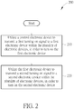
- Fig. 2 is a flowchart illustrating a method for performing power management in an electronic system according to an embodiment of the present invention.
- the method may be applied to the apparatus 100 shown in Fig. 1 , and more particularly, to the processing circuit 110 executing the program code.
- a computer programmable product such as a compact disc (CD) storing the program code
- a user or an administrator of the electronic system may configure the program code in the apparatus 100, wherein the computer programmable product comprises the program code (more particularly an installation version thereof) for indicating the processor to perform the method 200 shown in Fig. 2 .
- the processing circuit 110 may control operations of the electronic system (more particularly the electronic device 105), to perform the method 200 shown in Fig. 2 .
- the method is described in the following section.
- the electronic system utilizes the control electronic device to transmit a first turning on signal to the first electronic device within the plurality of electronic devices in order to trigger to turn on the first electronic device.
- the power management circuit 130 of the control electronic device may transmit the first turning on signal to the first electronic device through the interface circuit 120 of the control electronic device in order to trigger to turn on the first electronic device.
- the first electronic device may be turned on by the first turning on signal.
- the power management circuit 130 of the first electronic device may receive the first turning on signal through the interface circuit 120 of the first electronic device.
- the power management circuit 130 of the first electronic device may provide power to the processing circuit 110 of the first electronic device in response to triggering of the first turning on signal in order to trigger to turn on the first electronic device, wherein the first electronic device may represent a specific electronic device within the plurality of electronic devices except for the control electronic device.
- the electronic system utilizes the first electronic device to transmit a second turning on signal to the second electronic device within the plurality of electronic devices in order to trigger to turn on the second electronic device, wherein the second electronic device is coupled to the control electronic device through the first electronic device.
- the power management circuit 130 of the first electronic device may transmit the second turning on signal to the second electronic device through an interface circuit 120 of the first electronic device in order to trigger to turn on the second electronic device.
- the second electronic device is turned on by the second turning on signal.
- the power management circuit 130 of the second electronic device may receive the second turning on signal through the interface circuit 120 of the second electronic device.
- the power management circuit 130 of the second electronic device may provide power to the processing circuit 110 of the second electronic device due to the trigger of the second turning on signal in order to trigger to turn on the second electronic device.
- the control electronic device (more particularly the power management circuit 130 therein) may utilize the first electronic device to transmit the second turning on signal to the second electronic device in order to trigger to turn on the second electronic device, wherein the second electronic device may represent a specific electronic device within the plurality of electronic devices except for the control electronic device and the first electronic device.
- control electronic device may be implemented as the aforementioned enclosure according to the SAS expander technique, and any of the plurality of electronic devices except for the control electronic device may be implemented as the aforementioned enclosure according to the SAS expander technique.
- the plurality of electronic devices may be coupled in series in a string through a plurality of cables (e.g. the cables conforming to the SAS specification).
- the timing of triggering to turn on the second electronic device may be later than the timing of triggering to turn on the first electronic device, in order to prevent the overall instantaneous power consumption of the electronic system from exceeding a predetermined instantaneous power consumption upper bound value.
- the plurality of electronic devices may comprise a first set of electronic devices and a second set of electronic devices, and the first set of electronic devices may comprise the first electronic device and the second electronic device.
- an electronic device within the first set of electronic devices may transmit a turning on signal to an electronic device within the second set of electronic devices in order to trigger to turn on the second set of electronic devices, wherein the second set of electronic devices are coupled to the first set of electronic devices.
- the timing of triggering to turn on the second set of electronic devices may be later than the timing of triggering to turn on the first set of electronic devices, in order to prevent the overall instantaneous power consumption of the electronic system from exceeding the predetermined instantaneous power consumption upper bound value.
- the plurality of electronic devices may comprise at least another set of electronic devices, such as a third set of electronic devices.
- An electronic device within the second set of electronic devices may transmit a turning on signal to an electronic device within the third set of electronic devices in order to trigger to turn on the third set of electronic devices, wherein the third set of electronic devices are coupled to the first set of electronic devices through the second set of electronic devices.
- the timing of triggering to turn on the third set of electronic devices may be later than the timing of triggering to turn on the second set of electronic devices, in order to prevent the overall instantaneous power consumption of the electronic system from exceeding the predetermined instantaneous power consumption upper bound value.
- each of these turning on signals (e.g. the first turning on signal, the second turning on signal, etc.) may contain series data with a specific pattern, which can prevent a situation where the electronic devices couple to a wrong device through cables and are thus accidentally turned on.
- the control electronic device may divide the plurality of electronic devices into a plurality of sets of electronic devices, for turning on the electronic devices set by set. More particularly, according to respective power consumption information of at least a portion of (e.g. part or all of) the plurality of electronic devices and the predetermined instantaneous power consumption upper bound value (e.g. the power consumption information of the electronic device 105), the control electronic device may configure the number of the electronic devices within the plurality of electronic devices divided into the first set of electronic devices, in order to prevent the overall instantaneous power consumption of the electronic system from exceeding the predetermined instantaneous power consumption upper bound value.
- the predetermined instantaneous power consumption upper bound value e.g. the power consumption information of the electronic device 105
- the control electronic device may determine the number of electronic devices within the plurality of electronic devices divided into the plurality of sets of electronic devices, in order to prevent the overall instantaneous power consumption of the electronic system from exceeding the predetermined instantaneous power consumption upper bound value.
- the respective power consumption information of the aforementioned electronic devices may be information which is preloaded into the control electronic device, such as experimental data of the designer of the electronic system, the derivation data of the experimental data, the information predefined by the designer of electronic system, and/or the information predefined by the administrator of electronic system.
- the electronic system may pre-generate the respective power consumption information of the portion of electronic devices. More particularly, during a specific previous turning-on period of the electronic system, at least according to respective fundamental power consumption information of the portion of electronic devices (e.g.
- the control electronic device may estimate power consumption of the portion of electronic devices, respectively, to generate the respective power consumption information of the portion of electronic devices.
- control electronic device may store the respective power consumption information of the portion of electronic devices into a storage unit in the control electronic device, such as a non-volatile memory, to control the number of the electronic devices within the plurality of electronic devices divided into the first set of electronic devices, and/or controlling the number of the electronic devices within the plurality of electronic devices divided into a specific set of electronic devices, wherein the examples of the non-volatile memory may comprise (but are not limited to) an electrically erasable programmable read-only memory (EEPROM) and a flash memory.
- EEPROM electrically erasable programmable read-only memory
- the device for estimating respective power consumptions of the portion of electronic devices may comprise the control electronic device.
- the device for estimating the respective power consumptions of the portion of electronic devices may comprise the portion of electronic devices.
- the device for estimating the respective power consumptions of the portion of electronic devices may comprise the control electronic device and the portion of electronic devices.
- the electronic system may utilize the control electronic device to transmit the first turning on signal to the first electronic device in order to trigger to turn on the first electronic device, and may utilize the first electronic device to transmit the second turning on signal to the second electronic device in order to trigger to turn on the second electronic device.
- the electronic system may utilize the control electronic device to transmit a first turning off signal to the first electronic device to turn off the first electronic device.
- the electronic system may utilize the first electronic device to transmit a second turning off signal to the second electronic device to turn off the second electronic device.
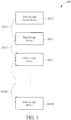
- Fig. 3 is a diagram illustrating a control scheme associated with the method 200 shown in Fig. 2 according to an embodiment of the present invention.
- a data storage system 300 may comprise a data storage control device 305-0 and N data storage devices 305-1, 305-2, ..., and 305-N (the symbol N may represent a positive integer larger than 1), wherein the data storage control device 305-0 and the N data storage devices 305-1, 305-2, ..., and 305-N may be coupled in series in a string through cables 350-2, ..., and 350-N.
- the data storage control device 305-0 may be implemented as the enclosure mentioned in the embodiment of Fig. 1 according to the SAS expander technique.
- each of the N data storage devices 305-1, 305-2, ..., and 305-N may also be implemented as the enclosure mentioned in the embodiment of Fig. 1 according to the SAS expander technique.
- an immediately prior device 305-(n - 1) may transmit a turning on signal to the specific data storage device 305-n in order to trigger to turn on the specific data storage device 305-n.
- the immediately prior device 305-(n - 1) may represent the data storage control device 305-0; in another example, if n > 1, the immediately prior device 305-(n - 1) may represent the data storage device 305-(n - 1).
- the data storage system 300 may be an example of the electronic system
- the data storage control device 305-0 may be an example of the control electronic device
- the N data storage devices 305-1, 305-2, ..., and 305-N may be examples of the electronic devices within the plurality of electronic devices except for the control electronic device.
- the first electronic device mentioned in Step 210 may represent a data storage device (e.g. the data storage device 305-1) within the N data storage devices 305-1, 305-2, ..., and 305-N
- the second electronic device mentioned in Step 220 may represent another data storage device (e.g. the data storage device 305-2) within the N data storage devices 305-1, 305-2, ..., and 305-N.
- the timing of triggering to turn on data storage device 305-n0 may be later than the timing of triggering to turn on the data storage device 305-(n0 - 1), to prevent the overall instantaneous power consumption of the electronic system from exceeding a predetermined instantaneous power consumption upper bound value.
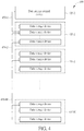
- Fig. 4 is a diagram illustrating a control scheme associated with the method shown in Fig. 2 according to another embodiment of the present invention.
- a data storage system 400 may comprise a data storage control device 405-0 and M sets of data storage devices 405-1, 405-2, ..., and 405-M (the symbol M may represent a positive integer larger than 1), wherein the data storage control device 405-0 and the M sets of data storage devices 405-1, 405-2, ..., and 405-M may be coupled in series in a string through cables 450-1, 450-2, ..., and 450-M.
- the data storage system 400 may be an example of the data storage system 300
- the data storage control device 405-0 may be an example of the data storage control device 305-0
- all the M sets of data storage devices 405-1, 405-2, ..., and 405-M may be an example of the N data storage devices 305-1, 305-2, ..., and 305-N.
- the M sets of data storage devices 405-1, 405-2, ..., and 405-M may be an example of the plurality of sets of electronic devices, wherein the sets of electronic devices may be obtained by dividing the data storage device.
- the aforementioned first set of electronic devices in this embodiment may represent the first set of data storage devices 405-1 within the M sets of data storage devices 405-1, 405-2, ..., and 405-M
- the aforementioned second set of electronic devices in this embodiment may represent the second set of data storage devices 405-2 within the M sets of data storage devices 405-1, 405-2, ..., and 405-M.
- the timing of triggering to turn on the set of data storage devices 405-m0 may be later than the timing of triggering to turn on the set of data storage devices 405-(m0 - 1), to prevent the overall instantaneous power consumption of the electronic system from exceeding the predetermined instantaneous power consumption upper bound value.
- the data storage control device 405-0 may provide a user interface for the administrator to set delay parameters.
- the data storage control device 405-0 may refer to the delay parameters to preset the delay time of transmitting a turning on signal to a next data storage device when a current data storage device receives a turning on signal in order to control the sets of the data storage devices, wherein the data storage control device 405-0 may set the delay time between any two data storage devices within the same set as 0. Hence, the data storage control device 405-0 may transmit a turning on signal to the data storage device 305-1 within the first set of data storage devices 405-1. The data storage device 305-1 is turned on immediately after receiving the turning on signal, and then transmits a turning on signal to the data storage device 305-2 within the first set of data storage devices 405-1 without waiting for a delay time.
- the data storage device 305-2 is turned on when receiving the turning on signal, and the rest can be done in the same manner.
- the first set of data storage devices 405-1 may turn on simultaneously. Since the turning on interval between the last data storage device within the first set of data storage devices 405-1 and the first data storage device within the second set of data storage devices 405-2 may be preset as a positive value, the timing of triggering to turn on the second set of data storage devices 405-2 will be delayed, and the rest can be done in the same manner.
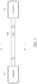
- Fig. 5 is a diagram illustrating a cable 500 associated with the method 200 shown in Fig. 2 according to an embodiment of the present invention.
- the cable 500 may be an example of any of the cables 350-1, 350-2, ..., and 350-N.
- the connectors 511 and 512 are configured at the two ends of the cable 500. This is merely for illustrative purposes, and not meant to be limitations of the present invention. For example, the shapes and forms of the connector 511 and 512 can be modified.
- Fig. 6 is a diagram illustrating an inner structure of the cable 500 shown in Fig. 5 , and more particularly, a cross section view along A-A', wherein the shaded part represents metal.
- the cable 500 comprises eight sets of high speed signal traces and two sets of low speed signal traces, wherein each set of high speed signal traces within the eight sets of high speed signal traces is cladded by the signal reference layer, and each set of high speed signal traces mentioned above in this embodiment may be called a signal differential pair.
- the outmost layer of the cable 500 is the isolating layer, and the isolating layer clads the cladding layer of the cable 500, wherein the cladding layer clads these eight sets of high speed signal traces and these two sets of low speed signal traces.
- the aforementioned signal reference layer and the cladding layer in the cable 500 may electrically connect to each other.
- the result is that both the aforementioned signal reference layer and cladding layer are electrically connected to the respective chassis grounds of the connectors 511 and 512.
- the electronic system may utilize the eight sets of high speed signal traces to perform data access or information exchange (e.g. exchanging information related to power management between the plurality of electronic devices).
- Any one set of low speed signal traces in the two sets of low speed signal trace may transmit or receive a turning on signal (e.g. the first turning on signal or the second turning on signal), and may also transmit or receive a turning off signal (e.g. the first turning off signal or the second turning off signal).
- a turning on signal may be transmitted through the low speed signal trace shown in Fig. 6 .
- the cable 500 in these embodiments may conform to the SAS 3.0 specification.
- a turning off signal may be transmitted through the high speed signal trace shown in Fig. 6 .
- Fig. 7 is a diagram illustrating a cable 600 associated with the method 200 shown in Fig. 2 according to another embodiment of the present invention.
- the cable 600 may be an example of any of the cables 350-1, 350-2, ..., and 350-N.
- the two ends of the cable 600 are installed with connectors 611 and 612, respectively. This is merely for illustrative purposes, and not meant to be limitations of the present invention.
- the shapes and forms of the connectors 611 and 612 can be modified.
- Fig. 8 is a diagram illustrating an inner structure of the cable 600 shown in Fig. 7 , and more particularly, the cross-sectional view along B-B', wherein the shaded part represents metal.
- the cable 600 comprises eight sets of high speed signal traces, wherein each set of high speed signal traces within the eight sets of high speed signal traces is cladded by a signal reference layer, and the aforementioned sets of high speed signal traces in this embodiment may be called a signal differential pair.
- the outmost layer of the cable 600 is an isolating layer, and the isolating layer clads the cladding layer of the cable 600, wherein the cladding layer clads the eight sets of high speed signal traces.
- the signal reference layer in the cable 600 and the cladding layer may be electrically connected.
- the electronic system may utilize the eight sets of high speed signal traces to perform data access, or perform information exchange (e.g. exchanging information related to power management between the plurality of electronic devices).
- the turning on signal may be transmitted through the signal reference layer shown in Fig. 8 , wherein these signal reference layers are electrically connected to the respective chassis grounds of the connectors 611 and 612.
- the cable 600 in these embodiments may conform to the SAS 2.0 specification.
- a turning off signal may be transmitted through the high speed signal trace shown in Fig. 8 .
- Fig. 9 is a diagram illustrating a signal transmission scheme associated with the method 200 shown in Fig. 2 according to an embodiment of the present invention.
- the electronic device 905 may represent the data storage control device 305-0.
- the electronic device 905 may represent a specific data storage device 305-n.
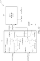
- the interface circuit 120 in this embodiment may comprise a connector 123, a switching unit 125 and at least one set of selecting paths, such as a signal path and a ground path, wherein the signal path may comprise the partial paths 127CON and 127SIG, and the ground path may comprise the partial paths 127CON and 127GND.
- the switching unit 125 may be implemented with at least one switch such as at least one metal oxide semiconductor field effect transistor (MOSFET). This is merely for illustrative purposes, and not meant to be limitations of the present invention.
- MOSFET metal oxide semiconductor field effect transistor
- the power management circuit 130 may generate a switching control signal 125CTRL, and may utilize the switching control signal 125CTRL to control switching operations of the switching unit 125, to selectively enable one of the signal path and the ground path and disable the other of the signal path and the ground path.
- the power management circuit 130 may utilize the switching control signal 125CTRL to enable the signal path to make the chassis ground 123CHGND in the connector 123 of the interface circuit 120 electrically connect to a signal terminal 130SIG of the power management circuit 130, rather than electrically connecting to a specific ground terminal 105GND of the electronic device 105.
- the power management circuit 130 may utilize the switching control signal 125CTRL to enable the ground path, making the chassis ground 123CHGND electrically connect to the specific ground terminal 105GND rather than electrically connecting to the signal terminal 130SIG.
- the power management circuit 130 may utilize the signal reference layer in the cable 600 to perform signal transmissions, wherein the signal reference layer may transmit or receive a turning on signal (e.g. the first turning on signal or the second turning on signal).
- the power management circuit 130 may control the switching unit 125 to enable the signal path, and prevent the chassis ground 123CHGND from electrically connecting to the specific ground terminal 105GND. Further, when the electronic device 105 performs data access operations, the power management circuit 130 may control the switching unit 125 to enable the ground path, in order to maintain the optimized impedance characteristic of the cable 600.
- the high speed signal in the eight sets of high speed signal traces may be correctly transmitted. Note that, compared with the high speed signal in eight sets of high speed signal traces, the turning on signal may be viewed as an OOB signal.
- Fig. 10 is a diagram illustrating a signal transmission scheme associated with the method shown in Fig. 2 according to another embodiment of the present invention.
- the electronic device 1005 in Fig. 10 may represent a specific data storage device 305-n. Since the specific data storage device 305-n comprises two connectors to be coupled as the data storage system 300 shown in Fig. 3 , the interface circuit 120 in this embodiment may comprise connectors ⁇ 123-1, 123-2 ⁇ , a switching unit ⁇ 125-1, 125-2 ⁇ and two sets of selecting paths, corresponding to the connector 123, the switching unit 125 and the set of selecting paths shown in the embodiment of Fig.
- the way in which the data storage control device 305-0 indicates the data storage device 305-1 to turn on can be modified.
- the data storage control device 305-0 may transmit a turning on signal to the data storage device 305-1 after learning that the data storage device 305-1 is connected to the data storage control device 305-0.
- the power management circuit 130 of the data storage device 305-1 will pull up the level of the chassis ground 123CHGND (1) of the connector 123-1, wherein the power management circuit 130 of the data storage device 305-1 may electrically connect the chassis ground 123CHGND (1) to the signal terminal 130SIG (1) thereof in advance, to facilitate pulling up the level.
- the data storage control device 305-0 may know that the data storage device 305-1 is coupled to the data storage control device 305-0.
- the data storage control device 305-0 may transmit a turning on signal to the data storage device 305-1 to turn on the data storage device 305-1, and disable the OOB signal path of the data storage control device 305-0 (i.e. by electrically connecting the chassis ground 123CHGND of connector 123 of the data storage control device 305-0 to a specific ground terminal 105GND of the data storage control device 305-0).
- the data storage device 305-1 When the data storage device 305-1 is turned on, the data storage device 305-1 may disable the OOB signal path corresponding to the connector 123-1 (i.e.
- the data storage control device 305-0 may utilize the high speed signal trace in the cable 350-1 to transmit a turning on confirmation signal to the data storage device 305-1, in order to confirm whether the data storage device 305-1 is successfully turned on. If the data storage control device 305-0 does not receive any confirmation signal from the data storage device 305-1 for a predetermined period (e.g. 5 or 10 sec), the data storage control device 305-0 may once again enable the OOB signal path of the connector 123 (i.e.
- the way in which the data storage device 305-1 turns on the data storage device 305-2 may be identical to the way in which the data storage control device 305-0 turns on the data storage device 305-1, wherein the connector 123-1 of the data storage device 305-2 may couple to the connector 123-2 of the data storage device 305-1; the remaining operations can be performed in the same manner.
- the data storage control device 305-0 may periodically transmit a turning on signal to the chassis ground 123CHGND of the connector 123 of the data storage control device 305-0.
- the power management circuit 130 of the data storage device 305-1 will receive the turning on signal and then turn on the data storage device 305-1, and disable the OOB signal path of the correspond to connector 123-1 (i.e. by electrically connecting the chassis ground 123CHGND (1) of the connector 123-1 of the data storage device 305-1 to the specific ground terminal 105GND of the data storage device 305-1). For example, after a predetermined period (e.g.
- the data storage control device 305-0 may utilize the high speed signal trace in the cable 350-1 to transmit a turning on confirmation signal to the data storage device 305-1, to confirm whether the data storage device 305-1 is successfully turned on. If the data storage control device 305-0 does not receive any confirmation signal sent back from the data storage device 305-1 for a predetermined period (e.g. 5 or 10 sec), the data storage control device 305-0 may once again turn on the OOB signal path of the connector 123, to once again transmit a turning on signal to the data storage device 305-1.
- a predetermined period e.g. 5 or 10 sec
- the way in which the data storage device 305-1 turns on the data storage device 305-2 may be identical to the way in which the data storage control device 305-0 turns on the data storage device 305-1, wherein the connector 123-1 of the data storage device 305-2 may couple to the connector 123-2 of the data storage device 305-1, and the remaining operations can be performed in the same manner.
- the power management circuit 130 of the data storage device 305-1 will disconnect both the chassis ground 123CHGND (1) of the connector 123-1 and the chassis ground 123CHGND (2) of the connector 123-2 from the specific ground terminal 105GND.
- the power management circuit 130 of the data storage device 305-1 When the data storage control device 305-0 indicates the data storage device 305-1 to enter a turned-on mode from the standby mode, the power management circuit 130 of the data storage device 305-1 will be electrically connected by the chassis ground 123CHGND (1) of the connector 123-1 to the specific ground terminal 105GND. Meanwhile, the power management circuit 130 of the data storage device 305-1 still continues disconnecting the chassis ground 123CHGND (2) of the control connector 123-2 from the specific ground terminal 105GND.
- the power management circuit 130 of the data storage device 305-1 may transmit a turning on signal to the data storage device 305-2 through an OOB signal path corresponding to the connector 123-2, and then electrically connect the chassis ground 123CHGND (2) of the connector 123-2 to the specific ground terminal 105GND.
- the power management circuit 130 of the specific data storage device 305-n may switch between the signal path of the connector 123-1 of the specific data storage device 305-n according to whether the specific data storage device 305-n is in the standby mode or in the turned-on mode. Further, the power management circuit 130 of the specific data storage device 305-n may switch between the signal path of the connector 123-2 of the specific data storage device 305-n according to whether the specific data storage device 305-n transmits a turning on signal to a next data storage device (e.g. the data storage device 305-(n + 1)), wherein the operation principles of the connector 123-2 of the specific data storage device 305-n may be identical to those of the connector 123 of the data storage control device 305-0.
- a next data storage device e.g. the data storage device 305-(n + 1)
- Fig. 11 is a diagram illustrating a signal transmission scheme associated with the method 200 shown in Fig. 2 according to yet another embodiment of the present invention.
- the electronic device 1105 in Fig. 11 may represent the data storage control device 305-0. In another example, the electronic device 1105 may represent the specific data storage device 305-n.
- the embodiment shown in Fig. 9 the configurations of the switching unit 125 and the set of selecting paths previously mentioned in the embodiment shown in Fig. 9 may be omitted in this embodiment.
- the connector 123 in this embodiment may comprise a set of low speed signal terminals 123LOW for coupling to the low speed signal traces shown in Fig. 6 , wherein the power management circuit 130 may comprise a corresponding set of low speed signal terminals 130LOW.
- the turning on signal may be transmitted by at least a portion of low speed signal trace within the low speed signal traces.
- the cable 500 in this embodiment may conform to the SAS 3.0 specification.
- the power management circuit 130 of the specific data storage device 305-n may comprise the set of low speed signal terminals 130LOW.
- the low speed signal traces in the cable 500 may be coupled to the set of low speed signal terminals 130LOW of the power management circuit 130 through the set of low speed signal terminals 123LOW.
- the data storage system 300 may comprise an enclosure (or a frame) for installing and fixing the data storage control device 305-0 and the data storage devices 305-1, 305-2, ..., 305-N.
- an enclosure or a frame
- the power supply will keep supplying power to the respective power management circuits ⁇ 130 ⁇ of the data storage control device 305-0 and the data storage devices 305-1, 305-2, ..., 305-N.
- the power supply may provide power to the power management circuits ⁇ 130 ⁇ only, thus avoiding various related art issues of large power consumption.
- the conventional data storage system operates continuously and thereby consumes much power; in another example, the conventional data storage system still consumes much power even when the HDD therein stops performing access operations. Therefore, the data storage system 300 of the present invention may achieve high power-saving in the standby mode.
- An advantage provided by the present invention is that the power consumption of the electronic system may be reduced. Take a scheme having two-headers and fifteen enclosures as example. The overall power consumption of the standby electronic system is about a hundred Watts (W). Compared with related arts, the method and associated device and computer programmable product of the present invention may greatly reduce the power consumption.
Landscapes
- Engineering & Computer Science (AREA)
- Theoretical Computer Science (AREA)
- General Engineering & Computer Science (AREA)
- Physics & Mathematics (AREA)
- General Physics & Mathematics (AREA)
- Computer Hardware Design (AREA)
- Computing Systems (AREA)
- Power Sources (AREA)
Description
- The present invention relates to the field of power management, such as the power management of a data storage system adopting a Serial Attached Small Computer System Interface (Serial Attached SCSI or SAS) technique, and more particularly, to a method for performing power management in an electronic system, and an associated apparatus.
- A conventional data storage system, such as those implemented with the SAS technique or an SAS expander, may lack a power management scheme. When the conventional data storage system is set up and provided with power, it may operate continuously, unless power outage or power failure occurs, in which case it will stop operating. In another example, when building a plurality of storage modules (e.g. a plurality of conventional enclosures) of the conventional data storage system and a conventional enclosure is installed to a cabinet (or a frame) which has the ability of providing power, the conventional enclosure will operate continuously unless power outage or power failure occurs.
- Since each conventional enclosure in the conventional data storage system may install more than twenty hard disk drives (HDDs), the overall power consumption of the conventional data storage system is very high. Without a proper power management scheme, much power will be consumed when the conventional data storage system accesses the hard disk drives therein. When a data access request is not needed, the access operation of each of the HDDs within the aforementioned conventional enclosure may be temporarily suspended, thus reducing the power consumption thereof. Taking a scheme comprising two headers and fifteen enclosures as an example, however, the overall power consumption of the conventional data storage system may still exceed 3500 Watts. U.S. Patent Application Publication No.
US 2011/099396 A1 and U.S. Patent Application Publication No.US 2011/099391 A1 that aim to reduce power consumption of a storage system having extension apparatus may be helpful on solving the power consumption problem, but correcting the problem without side effects has not been achieved. - From the above it is therefore demonstrated that the HDDs in the conventional data storage system consume much power when being accessed. Although the overall power consumption may be somewhat reduced due to suspending of the HDDs in each enclosure, the power consumption of the conventional data storage system is still very high. Therefore, there is a need for a novel method and an associated scheme to save power.
- This in mind, the application aims at providing a method and an associated apparatus for performing power management in an electronic system, to solve the aforementioned problems.
- This is achieved by methods of method for performing power management in an electronic system and associated apparatuses according to
claims 1, 6, 10 and 12. The dependent claims pertain to corresponding further developments and improvements. - As will be seen more clearly from the detailed description following below, a claimed method includes: when a first turning on signal transmitted from another electronic device within the plurality of electronic devices is received, utilizing a power management circuit of the first electronic device to provide power to a processing circuit of the first electronic device according to the first turning on signal in order to trigger to turn on the first electronic device, wherein the first electronic device is coupled to the other electronic device; and utilizing the power management circuit of the first electronic device to transmit a second turning on signal to a second electronic device within the plurality of electronic devices through an interface circuit of the first electronic device in order to trigger to turn on the second electronic device, wherein the second electronic device is coupled to the other electronic device through the first electronic device. For example, the power management circuit may receive the first turning on signal through a chassis ground of a connector of the interface circuit, and the interface circuit may comprise a switching unit arranged to switch between a signal path and a ground path, wherein the signal path locates between the chassis ground of the connector and a signal terminal of the power management circuit, and the ground path locates between the chassis ground of the connector and a specific ground terminal of the first electronic device. The method may further comprise: utilizing the power management circuit to generate a switching control signal, and utilizing the switching control signal to control a switching operation of the switching unit, to selectively enable one of the signal path and the ground path, and selectively disable the other of the signal path and the ground path. In addition to the above method, the present invention also provides a computer programmable product, wherein the computer programmable product includes a program code for indicating at least one processor to execute the above method, and the electronic system includes the aforementioned at least one processor.
- In addition, another claimed method includes: utilizing a power management circuit of the control electronic device to transmit a first turning on signal to a first electronic device within the plurality of electronic devices through an interface circuit of the control electronic device in order to trigger to turn on the first electronic device, wherein the first electronic device is coupled to the control electronic device; and when the first electronic device is turned on, utilizing the first electronic device to transmit a second turning on signal to a second electronic device within the plurality of electronic devices to turn the second electronic device, wherein the second electronic device is coupled to the control electronic device through the first electronic device. For example, the power management circuit of the control electronic device may transmit the first turning on signal through a chassis ground of a connector in the interface circuit of the control electronic device, and the interface circuit may comprise a switching unit arranged to switch between a signal path and a ground path, wherein the signal path locates between the chassis ground of the connector and a signal terminal of the power management circuit, and the ground path locates between the chassis ground of the connector and a specific ground terminal of the first electronic device. The method may further comprise: utilizing the power management circuit to generate a switching control signal, and utilizing the switching control signal to control a switching operation of the switching unit, to selectively enable one of the signal path and the ground path, and selectively disable the other of the signal path and the ground path.
- In addition, a claimed apparatus includes at least a portion of a first electronic device within a plurality of electronic devices of the data storage system. The apparatus includes a processing circuit, at least one interface circuit and a power management circuit. The processing circuit is arranged to control an operation of the first electronic device. The interface circuit is coupled to the processing circuit, and electrically connected to at least another electronic device within the plurality of electronic devices through at least one cable. The power management circuit is coupled to the interface circuit and the processing circuit. The power management circuit is arranged to control power of the processing circuit. When the power management circuit receives a first turning on signal transmitted by another electronic device within the plurality of electronic devices through the interface circuit, the power management circuit is arranged to turn on the processing circuit and is arranged to provide power to the processing circuit according to the first turning on signal. The first electronic device is coupled to the other electronic device through the interface circuit, and the power management circuit is arranged to transmit a second turning on signal to a second electronic device within the plurality of electronic devices through the interface circuit in order to trigger to turn on the second electronic device, wherein the second electronic device is coupled to the other electronic device through the first electronic device. For example, the interface circuit may comprise a connector comprising a chassis ground, and may comprise a switching unit that is coupled to the chassis ground of the connector. The power management circuit may be arranged to receive the first turning on signal through the chassis ground of the connector, and the switching unit may be arranged to switch between a signal path and a ground path, wherein the signal path locates between the chassis ground of the connector and a signal terminal of the power management circuit, and the ground path locates between the chassis ground of the connector and a specific ground terminal of the first electronic device. The power management circuit may be arranged to generate a switching control signal, and may be arranged to utilize the switching control signal to control a switching operation of the switching unit, to selectively enable one of the signal path and the ground path and disable the other of the signal path and the ground path. In addition to the above method, the present invention also correspondingly provides a computer program product. The computer program product includes a program code for indicating at least one processor to perform the above method, and the electronic system includes the processor.
- In addition, another claimed apparatus includes at least a portion of a control electronic device within a plurality of electronic devices of the data storage system. The apparatus includes a processing circuit, at least one interface circuit and a power management circuit. The processing circuit is arranged to control an operation of the control electronic device. The interface circuit is coupled to the processing circuit, and is arranged to electrically connect to at least another electronic device within the plurality of electronic devices through at least one cable to allow the control electronic device to control the data storage system. The power management circuit is coupled to the interface circuit and the processing circuit, and is arranged to control power of the processing circuit. The power management circuit is arranged to transmit a first turning on signal to a first electronic device within the plurality of electronic devices through the interface circuit in order to trigger to turn on the first electronic device, wherein the first electronic device is coupled to the control electronic device, and when the first electronic device is turned on, the power management circuit is arranged to utilize the first electronic device to transmit a second turning on signal to a second electronic device within the plurality of electronic devices in order to trigger to turn on the second electronic device, wherein the second electronic device is coupled to the control electronic device through the first electronic device. For example, the interface circuit may comprise a connector comprising a chassis ground, and may comprise a switching unit that is coupled to the chassis ground of the connector. The power management circuit may be arranged to transmit the first turning on signal through the chassis ground of the connector, and the switching unit may be arranged to switch between a signal path and a ground path, wherein the signal path locates between the chassis ground of the connector and a signal terminal of the power management circuit, and the ground path locates between the chassis ground of the connector and a specific ground terminal of the first electronic device. The power management circuit may be arranged to generate a switching control signal, and may be arranged to utilize the switching control signal to control a switching operation of the switching unit, to selectively enable one of the signal path and the ground path and selectively disable the other of the signal path and the ground path.
- In the following, the invention is further illustrated by way of example, taking reference to the accompanying drawings. Thereof:
- Fig. 1
- is a diagram illustrating an apparatus for performing power management in an electronic system according to an embodiment of the present invention,
- Fig. 2
- is a flowchart illustrating a method for performing power management in an electronic system according to an embodiment of the present invention,
- Fig. 3
- is a diagram illustrating a control scheme associated with the method shown in
Fig. 2 according to an embodiment of the present invention, - Fig. 4
- is a diagram illustrating a control scheme associated with the method shown in
Fig. 2 according to another embodiment of the present invention, - Fig. 5
- is a diagram illustrating a cable associated with the method shown in
Fig. 2 according to an embodiment of the present invention, - Fig. 6
- is a diagram illustrating an inner structure of the cable shown in
Fig. 5 , - Fig. 7
- is a diagram illustrating a cable associated with the method shown in
Fig. 2 according to another embodiment of the present invention, - Fig. 8
- is a diagram illustrating an inner structure of the cable shown in
Fig. 7 , - Fig. 9
- is a diagram illustrating a signal transmission scheme associated with the method shown in
Fig. 2 according to an embodiment of the present invention, - Fig. 10
- is a diagram illustrating a signal transmission scheme associated with the method shown in
Fig. 2 according to another embodiment of the present invention, and - Fig. 11
- is a diagram illustrating a signal transmission scheme associated with the method shown in
Fig. 2 according to yet another embodiment of the present invention. -
Fig. 1 is a diagram illustrating anapparatus 100 for performing power management in an electronic system according to an embodiment of the present invention, wherein the electronic system comprises a plurality of electronic devices, and theapparatus 100 may comprise at least a portion of (e.g. part or all of) the electronic system. For example, theapparatus 100 may be a control circuit in a specific electronic device within the plurality of electronic devices, such as an integrated circuit (IC) in the electronic device. In another example, theapparatus 100 may be the whole electronic device comprising the control circuit. In yet another example, theapparatus 100 may be at least two electronic devices within the plurality of electronic devices. In still another example, theapparatus 100 may be the whole electronic system. Examples of the electronic system may comprise (but are not limited to): a data storage system implemented with a serial attached small computer system interface (serial attached SCSI or SAS) technique, and a storage system implemented with the SAS Expander technique. Examples of the plurality of electronic devices may comprise (but are not limited to): a header and an enclosure implemented with the SAS expander technique. - As shown in
Fig. 1 , theapparatus 100 comprises: aprocessing circuit 110 installed in the electronic device such as theelectronic device 105; at least one interface circuit (e.g. one or more interface circuits, such as the interface circuit 120) coupled to theprocessing circuit 110 and installed in theelectronic device 105; and apower management circuit 130, coupled to the aforementioned interface circuit (e.g. the interface circuit 120) and theprocessing circuit 110, wherein thepower management circuit 130 is installed in theelectronic device 105. According to this embodiment, theprocessing circuit 110 is arranged to control operations of theelectronic device 105. Further, the interface circuit is used to electrically connect to at least another electronic device within the plurality of electronic devices through at least one cable. For example, theelectronic device 105 may be the control electronic device. In another example, theelectronic device 105 may be any of the plurality of electronic devices except for the control electronic device, e.g. theelectronic device 105 may be a first electronic device or a second electronic device. Further, thepower management circuit 130 is arranged to control the power of theprocessing circuit 110. Thepower management circuit 130 may selectively provide power to theprocessing circuit 110 or stop providing power to theprocessing circuit 110. For example, thepower management circuit 130 may continuously provide power to theprocessing circuit 110 to make theelectronic device 105 stay in a turned-on mode. In another example, thepower management circuit 130 may stop providing power to theprocessing circuit 110 to make theelectronic device 105 stay in a turned-off mode, wherein the turned-off mode is also known as a standby mode. - In practice, the control electronic device may be implemented as the enclosure mentioned in this embodiment according to the SAS expander technique, and any of the plurality of electronic devices except for the control electronic device may be implemented as the enclosure mentioned in this embodiment according to the SAS expander technique, wherein no matter whether the
electronic device 105 represents the control electronic device or any of the plurality of electronic devices except for the control electronic device, the interface circuit (e.g. the interface circuit 120) may be implemented as a corresponding SAS interface circuit according to the SAS expander technique. Hence, the electronic system may be implemented as a data storage system according to the SAS expander technique. Further, one or more electronic devices within the plurality of electronic devices (e.g. all of the plurality of electronic devices, or any of the plurality of electronic devices except for the first electronic device and the second electronic device, etc.) may comprise a plurality of storage devices. More particularly, the plurality of storage devices comprise at least one hard disk drive (HDD) or at least one solid state drive (SSD), such as a plurality of HDDs and/or a plurality of SSDs. For example, the data storage system may be implemented as a server, and a user may access data in the data storage system through at least one network. Thepower management circuit 130 may be executing a program code, and theprocessing circuit 110 executing the program code may control operations of theelectronic device 105 to provide services for users. If necessary, theprocessing circuit 110 executing the program code may execute settings related to power management (e.g. setting a power-on group), and obtain power consumption information of theelectronic device 105, such as the power of theelectronic device 105 in a sleep mode, the instantaneous power of theelectronic device 105 just awakened from a standby mode, or the power of theelectronic device 105 in a normal operation mode, wherein the program code may represent programs executed in theelectronic device 105, and more particularly, represent at least one program module such as at least one software module. This is merely for illustrative purposes, and not meant to be limitations of the present invention. According to some modifications of this embodiment, a program code may be embedded in theprocessing circuit 110, and the aforementioned program module may be a hardware circuit, such as at least a portion of (e.g. part or all of) theprocessing circuit 110. -
Fig. 2 is a flowchart illustrating a method for performing power management in an electronic system according to an embodiment of the present invention. The method may be applied to theapparatus 100 shown inFig. 1 , and more particularly, to theprocessing circuit 110 executing the program code. By utilizing a computer programmable product such as a compact disc (CD) storing the program code, a user or an administrator of the electronic system may configure the program code in theapparatus 100, wherein the computer programmable product comprises the program code (more particularly an installation version thereof) for indicating the processor to perform themethod 200 shown inFig. 2 . Hence, theprocessing circuit 110 may control operations of the electronic system (more particularly the electronic device 105), to perform themethod 200 shown inFig. 2 . The method is described in the following section. - In
Step 210, the electronic system utilizes the control electronic device to transmit a first turning on signal to the first electronic device within the plurality of electronic devices in order to trigger to turn on the first electronic device. For example, thepower management circuit 130 of the control electronic device may transmit the first turning on signal to the first electronic device through theinterface circuit 120 of the control electronic device in order to trigger to turn on the first electronic device. When the first turning on signal transmitted from the control electronic device is received, the first electronic device may be turned on by the first turning on signal. For example, thepower management circuit 130 of the first electronic device may receive the first turning on signal through theinterface circuit 120 of the first electronic device. More particularly, when the first turning on signal is received, thepower management circuit 130 of the first electronic device may provide power to theprocessing circuit 110 of the first electronic device in response to triggering of the first turning on signal in order to trigger to turn on the first electronic device, wherein the first electronic device may represent a specific electronic device within the plurality of electronic devices except for the control electronic device. - In
Step 220, the electronic system utilizes the first electronic device to transmit a second turning on signal to the second electronic device within the plurality of electronic devices in order to trigger to turn on the second electronic device, wherein the second electronic device is coupled to the control electronic device through the first electronic device. For example, thepower management circuit 130 of the first electronic device may transmit the second turning on signal to the second electronic device through aninterface circuit 120 of the first electronic device in order to trigger to turn on the second electronic device. When the second turning on signal transmitted from the first electronic device is received, the second electronic device is turned on by the second turning on signal. For example, thepower management circuit 130 of the second electronic device may receive the second turning on signal through theinterface circuit 120 of the second electronic device. More particularly, when the second turning on signal is received, thepower management circuit 130 of the second electronic device may provide power to theprocessing circuit 110 of the second electronic device due to the trigger of the second turning on signal in order to trigger to turn on the second electronic device. Hence, by turning on the first electronic device, the control electronic device (more particularly thepower management circuit 130 therein) may utilize the first electronic device to transmit the second turning on signal to the second electronic device in order to trigger to turn on the second electronic device, wherein the second electronic device may represent a specific electronic device within the plurality of electronic devices except for the control electronic device and the first electronic device. - According to this embodiment, the control electronic device may be implemented as the aforementioned enclosure according to the SAS expander technique, and any of the plurality of electronic devices except for the control electronic device may be implemented as the aforementioned enclosure according to the SAS expander technique. For example, the plurality of electronic devices may be coupled in series in a string through a plurality of cables (e.g. the cables conforming to the SAS specification).
- In practice, the timing of triggering to turn on the second electronic device may be later than the timing of triggering to turn on the first electronic device, in order to prevent the overall instantaneous power consumption of the electronic system from exceeding a predetermined instantaneous power consumption upper bound value.
- According to some embodiments, the plurality of electronic devices may comprise a first set of electronic devices and a second set of electronic devices, and the first set of electronic devices may comprise the first electronic device and the second electronic device. Further, an electronic device within the first set of electronic devices may transmit a turning on signal to an electronic device within the second set of electronic devices in order to trigger to turn on the second set of electronic devices, wherein the second set of electronic devices are coupled to the first set of electronic devices. More particularly, the timing of triggering to turn on the second set of electronic devices may be later than the timing of triggering to turn on the first set of electronic devices, in order to prevent the overall instantaneous power consumption of the electronic system from exceeding the predetermined instantaneous power consumption upper bound value. The plurality of electronic devices may comprise at least another set of electronic devices, such as a third set of electronic devices. An electronic device within the second set of electronic devices may transmit a turning on signal to an electronic device within the third set of electronic devices in order to trigger to turn on the third set of electronic devices, wherein the third set of electronic devices are coupled to the first set of electronic devices through the second set of electronic devices. More particularly, the timing of triggering to turn on the third set of electronic devices may be later than the timing of triggering to turn on the second set of electronic devices, in order to prevent the overall instantaneous power consumption of the electronic system from exceeding the predetermined instantaneous power consumption upper bound value. Note that each of these turning on signals (e.g. the first turning on signal, the second turning on signal, etc.) may contain series data with a specific pattern, which can prevent a situation where the electronic devices couple to a wrong device through cables and are thus accidentally turned on.
- In some embodiments, the control electronic device may divide the plurality of electronic devices into a plurality of sets of electronic devices, for turning on the electronic devices set by set. More particularly, according to respective power consumption information of at least a portion of (e.g. part or all of) the plurality of electronic devices and the predetermined instantaneous power consumption upper bound value (e.g. the power consumption information of the electronic device 105), the control electronic device may configure the number of the electronic devices within the plurality of electronic devices divided into the first set of electronic devices, in order to prevent the overall instantaneous power consumption of the electronic system from exceeding the predetermined instantaneous power consumption upper bound value. For example, according to the respective power consumption information of the aforementioned at least a portion of electronic devices within the plurality of electronic devices and the predetermined instantaneous power consumption upper bound value, the control electronic device may determine the number of electronic devices within the plurality of electronic devices divided into the plurality of sets of electronic devices, in order to prevent the overall instantaneous power consumption of the electronic system from exceeding the predetermined instantaneous power consumption upper bound value.
- In practice, the respective power consumption information of the aforementioned electronic devices may be information which is preloaded into the control electronic device, such as experimental data of the designer of the electronic system, the derivation data of the experimental data, the information predefined by the designer of electronic system, and/or the information predefined by the administrator of electronic system. This is merely for illustrative purposes, and not meant to be limitations of the present invention. According to some embodiments, the electronic system may pre-generate the respective power consumption information of the portion of electronic devices. More particularly, during a specific previous turning-on period of the electronic system, at least according to respective fundamental power consumption information of the portion of electronic devices (e.g. the power consumption of the
electronic device 105 when not mounting a storage device such as an HDD or SSD), respective storage device numbers of the portion of electronic devices (e.g. the number of HDDs and/or SSDs), and storage device power consumption information of the storage devices (e.g. the power consumption of each HDD and/or SSD), the control electronic device may estimate power consumption of the portion of electronic devices, respectively, to generate the respective power consumption information of the portion of electronic devices. Further, the control electronic device may store the respective power consumption information of the portion of electronic devices into a storage unit in the control electronic device, such as a non-volatile memory, to control the number of the electronic devices within the plurality of electronic devices divided into the first set of electronic devices, and/or controlling the number of the electronic devices within the plurality of electronic devices divided into a specific set of electronic devices, wherein the examples of the non-volatile memory may comprise (but are not limited to) an electrically erasable programmable read-only memory (EEPROM) and a flash memory. - In these embodiments, the device for estimating respective power consumptions of the portion of electronic devices (for generating respective power consumption information of the portion of electronic devices) may comprise the control electronic device. This is merely for illustrative purposes, and not meant to be limitations of the present invention. For example, the device for estimating the respective power consumptions of the portion of electronic devices may comprise the portion of electronic devices. In another example, the device for estimating the respective power consumptions of the portion of electronic devices may comprise the control electronic device and the portion of electronic devices.
- As mentioned above, the electronic system may utilize the control electronic device to transmit the first turning on signal to the first electronic device in order to trigger to turn on the first electronic device, and may utilize the first electronic device to transmit the second turning on signal to the second electronic device in order to trigger to turn on the second electronic device. For example, the electronic system may utilize the control electronic device to transmit a first turning off signal to the first electronic device to turn off the first electronic device. In another example, the electronic system may utilize the first electronic device to transmit a second turning off signal to the second electronic device to turn off the second electronic device.
-
Fig. 3 is a diagram illustrating a control scheme associated with themethod 200 shown inFig. 2 according to an embodiment of the present invention. As shown inFig. 3 , adata storage system 300 may comprise a data storage control device 305-0 and N data storage devices 305-1, 305-2, ..., and 305-N (the symbol N may represent a positive integer larger than 1), wherein the data storage control device 305-0 and the N data storage devices 305-1, 305-2, ..., and 305-N may be coupled in series in a string through cables 350-2, ..., and 350-N. For example, the data storage control device 305-0 may be implemented as the enclosure mentioned in the embodiment ofFig. 1 according to the SAS expander technique. Similarly, each of the N data storage devices 305-1, 305-2, ..., and 305-N may also be implemented as the enclosure mentioned in the embodiment ofFig. 1 according to the SAS expander technique. - According to this embodiment, regarding the data storage device 305-n within the N data storage devices 305-1, 305-2, ..., and 305-N (the symbol n may represent a positive integer with [1, N]), an immediately prior device 305-(n - 1) may transmit a turning on signal to the specific data storage device 305-n in order to trigger to turn on the specific data storage device 305-n. For example, if n = 1, the immediately prior device 305-(n - 1) may represent the data storage control device 305-0; in another example, if n > 1, the immediately prior device 305-(n - 1) may represent the data storage device 305-(n - 1). For better understanding, the
data storage system 300 may be an example of the electronic system, the data storage control device 305-0 may be an example of the control electronic device, and the N data storage devices 305-1, 305-2, ..., and 305-N may be examples of the electronic devices within the plurality of electronic devices except for the control electronic device. Hence, in this embodiment, the first electronic device mentioned inStep 210 may represent a data storage device (e.g. the data storage device 305-1) within the N data storage devices 305-1, 305-2, ..., and 305-N; and the second electronic device mentioned inStep 220 may represent another data storage device (e.g. the data storage device 305-2) within the N data storage devices 305-1, 305-2, ..., and 305-N. - In practice, regarding the data storage devices 305-(n0 - 1) and 305-n0 (the symbol n0 may represent a positive integer with [2, N]) within the N data storage devices 305-1, 305-2, ..., and 305-N electrically connected through the cable 350-n0, the timing of triggering to turn on data storage device 305-n0 may be later than the timing of triggering to turn on the data storage device 305-(n0 - 1), to prevent the overall instantaneous power consumption of the electronic system from exceeding a predetermined instantaneous power consumption upper bound value. Some features of this embodiment which are identical to those of the previous embodiments are omitted here for brevity.
-
Fig. 4 is a diagram illustrating a control scheme associated with the method shown inFig. 2 according to another embodiment of the present invention. As shown inFig. 4 , adata storage system 400 may comprise a data storage control device 405-0 and M sets of data storage devices 405-1, 405-2, ..., and 405-M (the symbol M may represent a positive integer larger than 1), wherein the data storage control device 405-0 and the M sets of data storage devices 405-1, 405-2, ..., and 405-M may be coupled in series in a string through cables 450-1, 450-2, ..., and 450-M. - For better understanding, the
data storage system 400 may be an example of thedata storage system 300, the data storage control device 405-0 may be an example of the data storage control device 305-0, and all the M sets of data storage devices 405-1, 405-2, ..., and 405-M may be an example of the N data storage devices 305-1, 305-2, ..., and 305-N. Hence, the M sets of data storage devices 405-1, 405-2, ..., and 405-M may be an example of the plurality of sets of electronic devices, wherein the sets of electronic devices may be obtained by dividing the data storage device. Further, the aforementioned first set of electronic devices in this embodiment may represent the first set of data storage devices 405-1 within the M sets of data storage devices 405-1, 405-2, ..., and 405-M, and the aforementioned second set of electronic devices in this embodiment may represent the second set of data storage devices 405-2 within the M sets of data storage devices 405-1, 405-2, ..., and 405-M. - In practice, regarding the sets of data storage devices 405-(m0 - 1) and 405-m0 (the symbol m0 may represent a positive integer within [2, M]) electrically connected to each other within the M sets of data storage devices 405-1, 405-2, ..., and 405-M,, the timing of triggering to turn on the set of data storage devices 405-m0 may be later than the timing of triggering to turn on the set of data storage devices 405-(m0 - 1), to prevent the overall instantaneous power consumption of the electronic system from exceeding the predetermined instantaneous power consumption upper bound value. For example, the data storage control device 405-0 may provide a user interface for the administrator to set delay parameters. The data storage control device 405-0 may refer to the delay parameters to preset the delay time of transmitting a turning on signal to a next data storage device when a current data storage device receives a turning on signal in order to control the sets of the data storage devices, wherein the data storage control device 405-0 may set the delay time between any two data storage devices within the same set as 0. Hence, the data storage control device 405-0 may transmit a turning on signal to the data storage device 305-1 within the first set of data storage devices 405-1. The data storage device 305-1 is turned on immediately after receiving the turning on signal, and then transmits a turning on signal to the data storage device 305-2 within the first set of data storage devices 405-1 without waiting for a delay time. The data storage device 305-2 is turned on when receiving the turning on signal, and the rest can be done in the same manner. Hence, the first set of data storage devices 405-1 may turn on simultaneously. Since the turning on interval between the last data storage device within the first set of data storage devices 405-1 and the first data storage device within the second set of data storage devices 405-2 may be preset as a positive value, the timing of triggering to turn on the second set of data storage devices 405-2 will be delayed, and the rest can be done in the same manner. Some features of this embodiment which are identical to those of the previous embodiments are omitted here for brevity.
-
Fig. 5 is a diagram illustrating acable 500 associated with themethod 200 shown inFig. 2 according to an embodiment of the present invention. Thecable 500 may be an example of any of the cables 350-1, 350-2, ..., and 350-N. Further, theconnectors cable 500. This is merely for illustrative purposes, and not meant to be limitations of the present invention. For example, the shapes and forms of theconnector -
Fig. 6 is a diagram illustrating an inner structure of thecable 500 shown inFig. 5 , and more particularly, a cross section view along A-A', wherein the shaded part represents metal. As shown inFig. 6 , thecable 500 comprises eight sets of high speed signal traces and two sets of low speed signal traces, wherein each set of high speed signal traces within the eight sets of high speed signal traces is cladded by the signal reference layer, and each set of high speed signal traces mentioned above in this embodiment may be called a signal differential pair. Further, the outmost layer of thecable 500 is the isolating layer, and the isolating layer clads the cladding layer of thecable 500, wherein the cladding layer clads these eight sets of high speed signal traces and these two sets of low speed signal traces. In practice, based on the inner structure shown inFig. 6 , the aforementioned signal reference layer and the cladding layer in thecable 500 may electrically connect to each other. Hence, when any of the aforementioned signal reference layer and cladding layer is electrically connected to the respective chassis grounds of theconnectors connectors Fig. 6 . In practice, thecable 500 in these embodiments may conform to the SAS 3.0 specification. Further, a turning off signal may be transmitted through the high speed signal trace shown inFig. 6 . -
Fig. 7 is a diagram illustrating acable 600 associated with themethod 200 shown inFig. 2 according to another embodiment of the present invention. Thecable 600 may be an example of any of the cables 350-1, 350-2, ..., and 350-N. Further, the two ends of thecable 600 are installed withconnectors connectors -
Fig. 8 is a diagram illustrating an inner structure of thecable 600 shown inFig. 7 , and more particularly, the cross-sectional view along B-B', wherein the shaded part represents metal. As shown inFig. 8 , thecable 600 comprises eight sets of high speed signal traces, wherein each set of high speed signal traces within the eight sets of high speed signal traces is cladded by a signal reference layer, and the aforementioned sets of high speed signal traces in this embodiment may be called a signal differential pair. Further, the outmost layer of thecable 600 is an isolating layer, and the isolating layer clads the cladding layer of thecable 600, wherein the cladding layer clads the eight sets of high speed signal traces. In practice, based on the inner structure shown inFig. 8 , the signal reference layer in thecable 600 and the cladding layer may be electrically connected. Hence, when any of the signal reference layer and the cladding layer is electrically connected to the respective chassis grounds of theconnectors connectors - According to some embodiments, the turning on signal may be transmitted through the signal reference layer shown in
Fig. 8 , wherein these signal reference layers are electrically connected to the respective chassis grounds of theconnectors cable 600 in these embodiments may conform to the SAS 2.0 specification. Further, a turning off signal may be transmitted through the high speed signal trace shown inFig. 8 . -
Fig. 9 is a diagram illustrating a signal transmission scheme associated with themethod 200 shown inFig. 2 according to an embodiment of the present invention. For example, theelectronic device 905 may represent the data storage control device 305-0. In another example, theelectronic device 905 may represent a specific data storage device 305-n. Theinterface circuit 120 in this embodiment may comprise aconnector 123, aswitching unit 125 and at least one set of selecting paths, such as a signal path and a ground path, wherein the signal path may comprise the partial paths 127CON and 127SIG, and the ground path may comprise the partial paths 127CON and 127GND. Further, theswitching unit 125 may be implemented with at least one switch such as at least one metal oxide semiconductor field effect transistor (MOSFET). This is merely for illustrative purposes, and not meant to be limitations of the present invention. - As shown in
Fig. 9 , thepower management circuit 130 may generate a switching control signal 125CTRL, and may utilize the switching control signal 125CTRL to control switching operations of theswitching unit 125, to selectively enable one of the signal path and the ground path and disable the other of the signal path and the ground path. For example, thepower management circuit 130 may utilize the switching control signal 125CTRL to enable the signal path to make the chassis ground 123CHGND in theconnector 123 of theinterface circuit 120 electrically connect to a signal terminal 130SIG of thepower management circuit 130, rather than electrically connecting to a specific ground terminal 105GND of theelectronic device 105. In another example, thepower management circuit 130 may utilize the switching control signal 125CTRL to enable the ground path, making the chassis ground 123CHGND electrically connect to the specific ground terminal 105GND rather than electrically connecting to the signal terminal 130SIG. - Since the chassis ground 123CHGND may be electrically connected to the chassis ground of one of the
connectors cable 600 is electrically connected to the respective chassis grounds of theconnectors cable 600 is electrically connected to theinterface circuit 120 and thepower management circuit 130 utilizes the switching control signal 125CTRL to enable the signal path, thepower management circuit 130 may utilize the signal reference layer in thecable 600 to perform signal transmissions, wherein the signal reference layer may transmit or receive a turning on signal (e.g. the first turning on signal or the second turning on signal). When thepower management circuit 130 performs operations related to power management, thepower management circuit 130 may control theswitching unit 125 to enable the signal path, and prevent the chassis ground 123CHGND from electrically connecting to the specific ground terminal 105GND. Further, when theelectronic device 105 performs data access operations, thepower management circuit 130 may control theswitching unit 125 to enable the ground path, in order to maintain the optimized impedance characteristic of thecable 600. Hence, the high speed signal in the eight sets of high speed signal traces may be correctly transmitted. Note that, compared with the high speed signal in eight sets of high speed signal traces, the turning on signal may be viewed as an OOB signal. -
Fig. 10 is a diagram illustrating a signal transmission scheme associated with the method shown inFig. 2 according to another embodiment of the present invention. Theelectronic device 1005 inFig. 10 may represent a specific data storage device 305-n. Since the specific data storage device 305-n comprises two connectors to be coupled as thedata storage system 300 shown inFig. 3 , theinterface circuit 120 in this embodiment may comprise connectors {123-1, 123-2}, a switching unit {125-1, 125-2} and two sets of selecting paths, corresponding to theconnector 123, theswitching unit 125 and the set of selecting paths shown in the embodiment ofFig. 9 , respectively, wherein the partial paths {127CON (1), 127CON (2)}, {127SIG (1), 127SIG (2)} and {127GND (1), 127GND (2)} correspond to the partial paths 127CON, 127SIG and 127GND, respectively, the chassis grounds {123CHGND (1), 123CHGND (2)} and {130SIG (1), 130SIG (2)} correspond to the chassis ground 123CHGND and the signal terminal 130SIG, and the switching control signals {125CTRL (1), 125CTRL (2)} correspond to the switching control signal 125CTRL. Some features of this embodiment which are identical to those of the previous embodiments are omitted here for brevity. - According to some embodiments, the way in which the data storage control device 305-0 indicates the data storage device 305-1 to turn on can be modified. In an embodiment, the data storage control device 305-0 may transmit a turning on signal to the data storage device 305-1 after learning that the data storage device 305-1 is connected to the data storage control device 305-0. After the connector 123-1 of the data storage device 305-1 is coupled to the
connector 123 of the data storage control device 305-0, thepower management circuit 130 of the data storage device 305-1 will pull up the level of the chassis ground 123CHGND (1) of the connector 123-1, wherein thepower management circuit 130 of the data storage device 305-1 may electrically connect the chassis ground 123CHGND (1) to the signal terminal 130SIG (1) thereof in advance, to facilitate pulling up the level. Hence, the data storage control device 305-0 may know that the data storage device 305-1 is coupled to the data storage control device 305-0. The data storage control device 305-0 may transmit a turning on signal to the data storage device 305-1 to turn on the data storage device 305-1, and disable the OOB signal path of the data storage control device 305-0 (i.e. by electrically connecting the chassis ground 123CHGND ofconnector 123 of the data storage control device 305-0 to a specific ground terminal 105GND of the data storage control device 305-0). When the data storage device 305-1 is turned on, the data storage device 305-1 may disable the OOB signal path corresponding to the connector 123-1 (i.e. by electrically connecting the chassis ground 123CHGND (1) of the connector 123-1 of the data storage device 305-1 to a specific ground terminal 105GND of the data storage device 305-1). For example, after a predetermined period (e.g. 5 or 10 sec), the data storage control device 305-0 may utilize the high speed signal trace in the cable 350-1 to transmit a turning on confirmation signal to the data storage device 305-1, in order to confirm whether the data storage device 305-1 is successfully turned on. If the data storage control device 305-0 does not receive any confirmation signal from the data storage device 305-1 for a predetermined period (e.g. 5 or 10 sec), the data storage control device 305-0 may once again enable the OOB signal path of the connector 123 (i.e. by electrically connecting the chassis ground 123CHGND of theconnector 123 of the data storage control device 305-0 to the signal terminal 130SIG of the data storage control device 305-0), in order to transmit the turning on signal to the data storage device 305-1 again. Further, the way in which the data storage device 305-1 turns on the data storage device 305-2 may be identical to the way in which the data storage control device 305-0 turns on the data storage device 305-1, wherein the connector 123-1 of the data storage device 305-2 may couple to the connector 123-2 of the data storage device 305-1; the remaining operations can be performed in the same manner. - In another embodiment, the data storage control device 305-0 may periodically transmit a turning on signal to the chassis ground 123CHGND of the
connector 123 of the data storage control device 305-0. When the connector 123-1 of the data storage device 305-1 is coupled to theconnector 123 of the data storage control device 305-0, thepower management circuit 130 of the data storage device 305-1 will receive the turning on signal and then turn on the data storage device 305-1, and disable the OOB signal path of the correspond to connector 123-1 (i.e. by electrically connecting the chassis ground 123CHGND (1) of the connector 123-1 of the data storage device 305-1 to the specific ground terminal 105GND of the data storage device 305-1). For example, after a predetermined period (e.g. 5 or 10 sec), the data storage control device 305-0 may utilize the high speed signal trace in the cable 350-1 to transmit a turning on confirmation signal to the data storage device 305-1, to confirm whether the data storage device 305-1 is successfully turned on. If the data storage control device 305-0 does not receive any confirmation signal sent back from the data storage device 305-1 for a predetermined period (e.g. 5 or 10 sec), the data storage control device 305-0 may once again turn on the OOB signal path of theconnector 123, to once again transmit a turning on signal to the data storage device 305-1. Further, the way in which the data storage device 305-1 turns on the data storage device 305-2 may be identical to the way in which the data storage control device 305-0 turns on the data storage device 305-1, wherein the connector 123-1 of the data storage device 305-2 may couple to the connector 123-2 of the data storage device 305-1, and the remaining operations can be performed in the same manner. - In some embodiments, there are two connectors {123-1, 123-2} on the
interface circuit 120 of the data storage device 305-1, wherein the connector 123-1 is coupled to the data storage control device 305-0, and the connector 123-2 is coupled to the data storage device 305-2. Assuming that the data storage device 305-1 has coupled to the data storage control device 305-0, and the data storage device 305-2 has not yet coupled to the data storage device 305-1, when the data storage device 305-1 is in the standby mode, thepower management circuit 130 of the data storage device 305-1 will disconnect both the chassis ground 123CHGND (1) of the connector 123-1 and the chassis ground 123CHGND (2) of the connector 123-2 from the specific ground terminal 105GND. When the data storage control device 305-0 indicates the data storage device 305-1 to enter a turned-on mode from the standby mode, thepower management circuit 130 of the data storage device 305-1 will be electrically connected by the chassis ground 123CHGND (1) of the connector 123-1 to the specific ground terminal 105GND. Meanwhile, thepower management circuit 130 of the data storage device 305-1 still continues disconnecting the chassis ground 123CHGND (2) of the control connector 123-2 from the specific ground terminal 105GND. After that, when the data storage device 305-2 is coupled to the data storage device 305-1, thepower management circuit 130 of the data storage device 305-1 may transmit a turning on signal to the data storage device 305-2 through an OOB signal path corresponding to the connector 123-2, and then electrically connect the chassis ground 123CHGND (2) of the connector 123-2 to the specific ground terminal 105GND. - In some embodiments, the
power management circuit 130 of the specific data storage device 305-n may switch between the signal path of the connector 123-1 of the specific data storage device 305-n according to whether the specific data storage device 305-n is in the standby mode or in the turned-on mode. Further, thepower management circuit 130 of the specific data storage device 305-n may switch between the signal path of the connector 123-2 of the specific data storage device 305-n according to whether the specific data storage device 305-n transmits a turning on signal to a next data storage device (e.g. the data storage device 305-(n + 1)), wherein the operation principles of the connector 123-2 of the specific data storage device 305-n may be identical to those of theconnector 123 of the data storage control device 305-0. -
Fig. 11 is a diagram illustrating a signal transmission scheme associated with themethod 200 shown inFig. 2 according to yet another embodiment of the present invention. Theelectronic device 1105 inFig. 11 may represent the data storage control device 305-0. In another example, theelectronic device 1105 may represent the specific data storage device 305-n. The embodiment shown inFig. 9 , the configurations of theswitching unit 125 and the set of selecting paths previously mentioned in the embodiment shown inFig. 9 may be omitted in this embodiment. Note that theconnector 123 in this embodiment may comprise a set of low speed signal terminals 123LOW for coupling to the low speed signal traces shown inFig. 6 , wherein thepower management circuit 130 may comprise a corresponding set of low speed signal terminals 130LOW. - According to this embodiment, the turning on signal may be transmitted by at least a portion of low speed signal trace within the low speed signal traces. In practice, the
cable 500 in this embodiment may conform to the SAS 3.0 specification. For example, thepower management circuit 130 of the specific data storage device 305-n may comprise the set of low speed signal terminals 130LOW. When thecable 500 is connected to theconnector 123 of theinterface circuit 120 of the specific data storage device 305-n through a specific connector thereof (e.g. theconnectors 511 or 512), the low speed signal traces in thecable 500 may be coupled to the set of low speed signal terminals 130LOW of thepower management circuit 130 through the set of low speed signal terminals 123LOW. Some features of this embodiment which are identical to those of the previous embodiments are omitted here for brevity. - According to some embodiments, the
data storage system 300 may comprise an enclosure (or a frame) for installing and fixing the data storage control device 305-0 and the data storage devices 305-1, 305-2, ..., 305-N. When respective power traces of the data storage control device 305-0 and the data storage devices 305-1, 305-2, ..., 305-N are coupled to the power supply in the enclosure, the power supply will keep supplying power to the respective power management circuits {130} of the data storage control device 305-0 and the data storage devices 305-1, 305-2, ..., 305-N. When all the data storage devices 305-1, 305-2, ..., 305-N are in the standby mode, the power supply may provide power to the power management circuits {130} only, thus avoiding various related art issues of large power consumption. For example, the conventional data storage system operates continuously and thereby consumes much power; in another example, the conventional data storage system still consumes much power even when the HDD therein stops performing access operations. Therefore, thedata storage system 300 of the present invention may achieve high power-saving in the standby mode. - An advantage provided by the present invention is that the power consumption of the electronic system may be reduced. Take a scheme having two-headers and fifteen enclosures as example. The overall power consumption of the standby electronic system is about a hundred Watts (W). Compared with related arts, the method and associated device and computer programmable product of the present invention may greatly reduce the power consumption.
Claims (12)
- A method for performing power management in a data storage system, the method applied to a first electronic device (105) within a plurality of electronic devices of the data storage system, the method comprising:when a first turning on signal transmitted from another electronic device within the plurality of electronic devices is received, utilizing a power management circuit (130) of the first electronic device (105) to provide power to a processing circuit (110) of the first electronic device (105) in response to the trigger of the first turning on signal in order to trigger to turn on the first electronic device (105), wherein the first electronic device (105) is coupled to the other electronic device; andutilizing the power management circuit (130) of the first electronic device (105) to transmit a second turning on signal to a second electronic device within the plurality of electronic devices through an interface circuit (120) of the first electronic device (105) in order to trigger to turn on the second electronic device, wherein the second electronic device is coupled to the other electronic device through the first electronic device (105);the method characterized in that the power management circuit (130) receives the first turning on signal through a chassis ground of a connector of the interface circuit (120); the interface circuit (120) comprises a switching unit arranged to switch between a signal path and a ground path, wherein the signal path is located between the chassis ground of the connector and a signal terminal of the power management circuit (130), and the ground path is located between the chassis ground of the connector and a specific ground terminal of the first electronic device (105); and the method further comprises:utilizing the power management circuit (130) to generate a switching control signal, and utilizing the switching control signal to control a switching operation of the switching unit, to selectively enable one of the signal path and the ground path, and selectively disable the other of the signal path and the ground path.
- The method of claim 1, characterized in that the power management circuit (130) transmits the second turning on signal through a chassis ground of another connector in the interface circuit (120); the interface circuit (120) comprises another switching unit arranged to switch between another signal path and another ground path, wherein the other signal path is located between the chassis ground of the other connector and another signal terminal of the power management circuit (130), and the other ground path is located between the chassis ground of the other connector and the specific ground terminal of the first electronic device (105); and the method further comprises:utilizing the power management circuit (130) to generate another switching control signal, and utilizing the other switching control signal to control a switching operation of the other switching unit, to selectively enable one of the other signal path and the other ground path and disable the other of the other signal path and the other ground path.
- The method of claim 1, characterized in that the power management circuit (130) receives the first turning on signal through a set of low speed signal terminals of the connector in the interface circuit (120) and a set of low speed signal terminals of the power management circuit (130).
- The method of claim 1, characterized in that a timing of triggering to turn on the second electronic device is later than a timing of triggering to turn on the first electronic device (105), to prevent an overall instantaneous power consumption of the data storage system from exceeding a predetermined instantaneous power consumption upper bound value.
- The method of claim 1, characterized in that the plurality of electronic devices comprises a first set of electronic devices and a second set of electronic devices, and the first set of electronic devices comprise the first electronic device (105) and the second electronic device; and an electronic device within the first set of electronic devices transmits a turning on signal to an electronic device within the second set of electronic devices in order to trigger to turn on the second set of electronic devices, wherein the second set of electronic devices are coupled to the first set of electronic devices; wherein a timing of triggering to turn on the second set of electronic devices is later than a timing of triggering to turn on the first set of electronic devices, to prevent an overall instantaneous power consumption of the data storage system from exceeding a predetermined instantaneous power consumption upper bound value.
- A method for performing power management in a data storage system, the method applied to a control electronic device (105) of a plurality of electronic devices of the data storage system, the method comprising:utilizing a power management circuit (130) of the control electronic device (105) to transmit a first turning on signal to a first electronic device within the plurality of electronic devices through an interface circuit (120) of the control electronic device (105) in order to trigger to turn on the first electronic device, wherein the first electronic device is coupled to the control electronic device (105); andwhen the first electronic device is turned on, utilizing the first electronic device to transmit a second turning on signal to a second electronic device within the plurality of electronic devices in order to trigger to turn on the second electronic device, wherein the second electronic device is coupled to the control electronic device (105) through the first electronic device;the method characterized in that the power management circuit (130) transmits the first turning on signal through a chassis ground of a connector in the interface circuit (120); the interface circuit (120) comprises a switching unit, arranged to switch between a signal path and a ground path, wherein the signal path is located between the chassis ground of the connector and a signal terminal of the power management circuit (130), and the ground path is located between the chassis ground of the connector and a specific ground terminal of the first electronic device; and the method further comprises:utilizing the power management circuit (130) to generate a switching control signal, and utilizing the switching control signal to control a switching operation of the switching unit, to selectively enable one of the signal path and the ground path, and selectively disable the other of the signal path and the ground path.
- The method of claim 6, characterized in that the plurality of electronic devices comprise a first set of electronic devices and a second set of electronic devices, and the first set of electronic devices comprise the first electronic device and the second electronic device; and an electronic device within the first set of electronic devices transmits a turning on signal to an electronic device within the second set of electronic devices in order to trigger to turn on the second set of electronic devices, wherein the second set of electronic devices are coupled to the first set of electronic devices; wherein a timing of triggering to turn on the second set of electronic devices is later than a timing of triggering to turn on the first set of electronic devices, to prevent an overall instantaneous power consumption of the data storage system from exceeding a predetermined instantaneous power consumption upper bound value.
- The method of claim 7, characterized in that the method further comprises:according to respective fundamental power consumption information of at least a portion of the electronic devices, respective numbers of storage devices of the portion of the electronic devices, and power consumption information of the storage devices, estimating respective power consumptions of the portion of the electronic devices, generating respective power consumption information of the portion of the electronic devices; andaccording to the respective power consumption information of the portion of the electronic devices and a predetermined instantaneous power consumption upper bound value, controlling a number of devices within the plurality of electronic devices divided into the first set of electronic devices.
- The method of claim 6, characterized in that each of the first turning on signal and the second turning on signal contains series data with a specific pattern.
- An apparatus (100) for performing power management in a data storage system, the apparatus (100) comprising at least a portion of a first electronic device (105) within a plurality of electronic devices of the data storage system, the apparatus (100) comprising:a processing circuit (110), arranged to control an operation of the first electronic device (105);at least one interface circuit (120), coupled to the processing circuit (110), and electrically connected to at least another electronic device within the plurality of electronic devices through at least one cable; anda power management circuit (130), coupled to the interface circuit (120) and the processing circuit (110), the power management circuit (130) arranged to control power of the processing circuit (110), wherein when the power management circuit (130) receives a first turning on signal transmitted from another electronic device within the plurality of electronic devices through the interface circuit (120), the power management circuit (130) is arranged to turn on the processing circuit (110) and is arranged to provide power to the processing circuit (110) in response to triggering of the first turning on signal, wherein the first electronic device (105) is coupled to the other electronic device through the interface circuit (120), and the power management circuit (130) is arranged to transmit a second turning on signal to a second electronic device within the plurality of electronic devices through the interface circuit (120), in order to trigger to turn on the second electronic device, wherein the second electronic device is coupled to the other electronic device through the first electronic device (105);the apparatus (100) characterized in that the interface circuit (120) comprises:wherein the power management circuit (130) is arranged to generate a switching control signal, and is arranged to utilize the switching control signal to control a switching operation of the switching unit, to selectively enable one of the signal path and the ground path and disable the other of the signal path and the ground path.a connector, wherein the connector comprises:a chassis ground, wherein the power management circuit (130) is arranged to receive the first turning on signal through the chassis ground of the connector; anda switching unit, coupled to the chassis ground of the connector, the switching unit arranged to switch between a signal path and a ground path, wherein the signal path is located between the chassis ground of the connector and a signal terminal of the power management circuit (130), and the ground path is located between the chassis ground of the connector and a specific ground terminal of the first electronic device (105);
- The apparatus (100) of claim 10, characterized in that the interface circuit (120) further comprises:another connector, comprising:a chassis ground, wherein the power management circuit (130) is arranged to transmit the second turning on signal through the chassis ground of the other connector; andanother switching unit, coupled to the chassis ground of the other connector, the other switching unit arranged to switch between another signal path and another ground path, wherein the other signal path is located between the chassis ground of the other connector and another signal terminal of the power management circuit (130), and the other ground path is located between the chassis ground of the other connector and the specific ground terminal of the first electronic device (105);wherein the power management circuit (130) is arranged to generate another switching control signal, and is arranged to utilize the other switching control signal to control a switching operation of the other switching unit, to selectively enable one of the other signal path and the other ground path and disable the other of the other signal path and the other ground path.
- An apparatus (100) for performing power management in a data storage system, the apparatus (100) comprising at least a portion of a control electronic device (105) within a plurality of electronic devices of the data storage system, the apparatus (100) comprising:a processing circuit (110), arranged to control an operation of the control electronic device (105);at least one interface circuit (120), coupled to the processing circuit (110), and the interface circuit (120) arranged to electrically connect to at least another electronic device within the plurality of electronic devices through at least one cable, to allow the control electronic device (105) to control the data storage system; anda power management circuit (130), coupled to the interface circuit (120) and the processing circuit (110), the power management circuit (130) arranged to control power of the processing circuit (110), wherein the power management circuit (130) is arranged to transmit a first turning on signal to a first electronic device within the plurality of electronic devices through the interface circuit (120) in order to trigger to turn on the first electronic device, wherein the first electronic device is coupled to the control electronic device (105), and when the first electronic device is turned on, the power management circuit (130) is arranged to utilize the first electronic device to transmit a second turning on signal to a second electronic device within the plurality of electronic devices in order to trigger to turn on the second electronic device, wherein the second electronic device is coupled to the control electronic device (105) through the first electronic device;the apparatus (100) characterized in that the interface circuit (120) comprises:a connector, wherein the connector comprises:a chassis ground, wherein the power management circuit (130) is arranged to transmit the first turning on signal through the chassis ground of the connector; anda switching unit, coupled to the chassis ground of the connector, the switching unit arranged to switch between a signal path and a ground path, wherein the signal path is located between the chassis ground of the connector and a signal terminal of the power management circuit (130), and the ground path is located between the chassis ground of the connector and a specific ground terminal of the first electronic device; wherein the power management circuit (130) is arranged to generate a switching control signal, and is arranged to utilize the switching control signal to control a switching operation of the switching unit, to selectively enable one of the signal path and the ground path and selectively disable the other of the signal path and the ground path.
Applications Claiming Priority (1)
| Application Number | Priority Date | Filing Date | Title |
|---|---|---|---|
| TW104113934A TWI545431B (en) | 2015-04-30 | 2015-04-30 | Method for performing power management in an electronic system, and associated apparatus |
Publications (2)
| Publication Number | Publication Date |
|---|---|
| EP3088988A1 EP3088988A1 (en) | 2016-11-02 |
| EP3088988B1 true EP3088988B1 (en) | 2018-03-21 |
Family
ID=55640647
Family Applications (1)
| Application Number | Title | Priority Date | Filing Date |
|---|---|---|---|
| EP16162819.3A Not-in-force EP3088988B1 (en) | 2015-04-30 | 2016-03-30 | Method and associated apparatus for performing power management in an electronic system |
Country Status (4)
| Country | Link |
|---|---|
| US (1) | US10162398B2 (en) |
| EP (1) | EP3088988B1 (en) |
| CN (1) | CN106095036B (en) |
| TW (1) | TWI545431B (en) |
Family Cites Families (13)
| Publication number | Priority date | Publication date | Assignee | Title |
|---|---|---|---|---|
| KR100256944B1 (en) * | 1997-07-31 | 2000-05-15 | 윤종용 | Alarm device for PCI hot plug |
| US7818559B2 (en) | 2007-02-28 | 2010-10-19 | Microsoft Corporation | Boot negotiation among multiple boot-capable devices |
| JP5288899B2 (en) | 2008-06-20 | 2013-09-11 | 株式会社日立製作所 | Storage apparatus for estimating power consumption and power estimation method for storage apparatus |
| CN101676825A (en) * | 2008-09-19 | 2010-03-24 | 宏碁股份有限公司 | Electronic system and power supply device thereof |
| JP4920658B2 (en) | 2008-10-20 | 2012-04-18 | 株式会社日立製作所 | Power estimation method and computer system |
| JP2011090577A (en) * | 2009-10-23 | 2011-05-06 | Fujitsu Ltd | Storage device, storage system and storage device starting method |
| JP5083290B2 (en) | 2009-10-23 | 2012-11-28 | 富士通株式会社 | Storage system |
| US8856501B2 (en) * | 2009-12-14 | 2014-10-07 | Sandisk Technologies Inc. | Method and system for controlling operation of interconnected devices by circulating host capability without a centralized manager |
| JP5755324B2 (en) * | 2010-08-31 | 2015-07-29 | スリーエム イノベイティブ プロパティズ カンパニー | Electrical characteristics of shielded electrical cable |
| JP5614204B2 (en) | 2010-09-24 | 2014-10-29 | ヤマハ株式会社 | Electronic equipment |
| TWI480800B (en) | 2013-01-25 | 2015-04-11 | Wistron Neweb Corp | Fast boot method and electronic system |
| US9454206B2 (en) * | 2013-12-30 | 2016-09-27 | Netapp, Inc. | Power management techniques for computer-readable storage devices |
| US9271390B2 (en) * | 2014-07-15 | 2016-02-23 | Freescale Semiconductor, Inc. | Semiconductor device with active shielding of leads |
-
2015
- 2015-04-30 TW TW104113934A patent/TWI545431B/en not_active IP Right Cessation
-
2016
- 2016-01-04 CN CN201610002988.4A patent/CN106095036B/en not_active Expired - Fee Related
- 2016-03-14 US US15/068,656 patent/US10162398B2/en not_active Expired - Fee Related
- 2016-03-30 EP EP16162819.3A patent/EP3088988B1/en not_active Not-in-force
Non-Patent Citations (1)
| Title |
|---|
| None * |
Also Published As
| Publication number | Publication date |
|---|---|
| US20160320817A1 (en) | 2016-11-03 |
| TWI545431B (en) | 2016-08-11 |
| CN106095036A (en) | 2016-11-09 |
| EP3088988A1 (en) | 2016-11-02 |
| TW201638716A (en) | 2016-11-01 |
| CN106095036B (en) | 2019-04-05 |
| US10162398B2 (en) | 2018-12-25 |
Similar Documents
| Publication | Publication Date | Title |
|---|---|---|
| CN106951051A (en) | A kind of running protection method of server backplane | |
| TW201202904A (en) | System and method for identifying power connections in computer systems having redundant power supplies | |
| CN111857308B (en) | Server power management method and system | |
| US8527795B2 (en) | Changing processor performance from a throttled state during a power supply failure | |
| CN106873745A (en) | A kind of system and method for realizing backboard voltage monitoring | |
| US9710051B2 (en) | Methods of power supply unit rotating in an information handling system | |
| CN105468122A (en) | Method and device for off-peak boot of nodes and whole cabinet server | |
| CN120596425A (en) | Server mainboard and link management method | |
| CN218824636U (en) | Power supply detection device for server hard disk backboard | |
| EP3401756A1 (en) | Method and associated apparatus for performing destination power management with aid of source data statistics in storage system | |
| CN116521416A (en) | Information processing method, device, equipment and medium | |
| US10162398B2 (en) | Method and associated apparatus for performing power management in an electronic system | |
| EP3115901B1 (en) | Method and associated apparatus for managing a storage system with aid of hybrid management paths | |
| US9323305B2 (en) | Power supply unit with configurable output rails | |
| US9466982B2 (en) | System and method for control of power consumption of information handling system devices | |
| US20240119980A1 (en) | Controlling memory module clock buffer power in a system with dual memory clocks per memory module | |
| US20230342321A1 (en) | Enhanced eye-width margin using duty cycle adjust | |
| CN117331423A (en) | Power supply method and device, storage medium and electronic device for PCIE equipment | |
| US9858135B2 (en) | Method and associated apparatus for managing a storage system | |
| TWI719461B (en) | Server power managing method and system thereof | |
| US20160366024A1 (en) | Method and associated apparatus for managing a storage system | |
| US12334187B2 (en) | Power reduction in a clock buffer of a memory module based upon memory module topology | |
| US12315594B2 (en) | Controlling memory module clock buffer power in a system with a single memory clock per memory module | |
| US12334188B2 (en) | Power reduction in a clock buffer of a memory module based upon memory module speed | |
| CN114089824B (en) | Hot plug part protection method and device |
Legal Events
| Date | Code | Title | Description |
|---|---|---|---|
| PUAI | Public reference made under article 153(3) epc to a published international application that has entered the european phase |
Free format text: ORIGINAL CODE: 0009012 |
|
| AK | Designated contracting states |
Kind code of ref document: A1 Designated state(s): AL AT BE BG CH CY CZ DE DK EE ES FI FR GB GR HR HU IE IS IT LI LT LU LV MC MK MT NL NO PL PT RO RS SE SI SK SM TR |
|
| AX | Request for extension of the european patent |
Extension state: BA ME |
|
| STAA | Information on the status of an ep patent application or granted ep patent |
Free format text: STATUS: REQUEST FOR EXAMINATION WAS MADE |
|
| 17P | Request for examination filed |
Effective date: 20170418 |
|
| RBV | Designated contracting states (corrected) |
Designated state(s): AL AT BE BG CH CY CZ DE DK EE ES FI FR GB GR HR HU IE IS IT LI LT LU LV MC MK MT NL NO PL PT RO RS SE SI SK SM TR |
|
| GRAP | Despatch of communication of intention to grant a patent |
Free format text: ORIGINAL CODE: EPIDOSNIGR1 |
|
| STAA | Information on the status of an ep patent application or granted ep patent |
Free format text: STATUS: GRANT OF PATENT IS INTENDED |
|
| INTG | Intention to grant announced |
Effective date: 20171012 |
|
| GRAS | Grant fee paid |
Free format text: ORIGINAL CODE: EPIDOSNIGR3 |
|
| GRAA | (expected) grant |
Free format text: ORIGINAL CODE: 0009210 |
|
| STAA | Information on the status of an ep patent application or granted ep patent |
Free format text: STATUS: THE PATENT HAS BEEN GRANTED |
|
| AK | Designated contracting states |
Kind code of ref document: B1 Designated state(s): AL AT BE BG CH CY CZ DE DK EE ES FI FR GB GR HR HU IE IS IT LI LT LU LV MC MK MT NL NO PL PT RO RS SE SI SK SM TR |
|
| REG | Reference to a national code |
Ref country code: GB Ref legal event code: FG4D |
|
| REG | Reference to a national code |
Ref country code: FR Ref legal event code: PLFP Year of fee payment: 3 |
|
| REG | Reference to a national code |
Ref country code: CH Ref legal event code: EP |
|
| REG | Reference to a national code |
Ref country code: CH Ref legal event code: NV Representative=s name: E. BLUM AND CO. AG PATENT- UND MARKENANWAELTE , CH |
|
| REG | Reference to a national code |
Ref country code: AT Ref legal event code: REF Ref document number: 981767 Country of ref document: AT Kind code of ref document: T Effective date: 20180415 |
|
| REG | Reference to a national code |
Ref country code: IE Ref legal event code: FG4D |
|
| REG | Reference to a national code |
Ref country code: DE Ref legal event code: R096 Ref document number: 602016002071 Country of ref document: DE |
|
| PGFP | Annual fee paid to national office [announced via postgrant information from national office to epo] |
Ref country code: DE Payment date: 20180315 Year of fee payment: 3 |
|
| PGFP | Annual fee paid to national office [announced via postgrant information from national office to epo] |
Ref country code: FR Payment date: 20180326 Year of fee payment: 3 |
|
| REG | Reference to a national code |
Ref country code: NL Ref legal event code: FP |
|
| PG25 | Lapsed in a contracting state [announced via postgrant information from national office to epo] |
Ref country code: CY Free format text: LAPSE BECAUSE OF FAILURE TO SUBMIT A TRANSLATION OF THE DESCRIPTION OR TO PAY THE FEE WITHIN THE PRESCRIBED TIME-LIMIT Effective date: 20180321 Ref country code: HR Free format text: LAPSE BECAUSE OF FAILURE TO SUBMIT A TRANSLATION OF THE DESCRIPTION OR TO PAY THE FEE WITHIN THE PRESCRIBED TIME-LIMIT Effective date: 20180321 Ref country code: LT Free format text: LAPSE BECAUSE OF FAILURE TO SUBMIT A TRANSLATION OF THE DESCRIPTION OR TO PAY THE FEE WITHIN THE PRESCRIBED TIME-LIMIT Effective date: 20180321 Ref country code: NO Free format text: LAPSE BECAUSE OF FAILURE TO SUBMIT A TRANSLATION OF THE DESCRIPTION OR TO PAY THE FEE WITHIN THE PRESCRIBED TIME-LIMIT Effective date: 20180621 Ref country code: FI Free format text: LAPSE BECAUSE OF FAILURE TO SUBMIT A TRANSLATION OF THE DESCRIPTION OR TO PAY THE FEE WITHIN THE PRESCRIBED TIME-LIMIT Effective date: 20180321 |
|
| REG | Reference to a national code |
Ref country code: LT Ref legal event code: MG4D |
|
| REG | Reference to a national code |
Ref country code: AT Ref legal event code: MK05 Ref document number: 981767 Country of ref document: AT Kind code of ref document: T Effective date: 20180321 |
|
| PG25 | Lapsed in a contracting state [announced via postgrant information from national office to epo] |
Ref country code: SE Free format text: LAPSE BECAUSE OF FAILURE TO SUBMIT A TRANSLATION OF THE DESCRIPTION OR TO PAY THE FEE WITHIN THE PRESCRIBED TIME-LIMIT Effective date: 20180321 Ref country code: LV Free format text: LAPSE BECAUSE OF FAILURE TO SUBMIT A TRANSLATION OF THE DESCRIPTION OR TO PAY THE FEE WITHIN THE PRESCRIBED TIME-LIMIT Effective date: 20180321 Ref country code: GR Free format text: LAPSE BECAUSE OF FAILURE TO SUBMIT A TRANSLATION OF THE DESCRIPTION OR TO PAY THE FEE WITHIN THE PRESCRIBED TIME-LIMIT Effective date: 20180622 Ref country code: RS Free format text: LAPSE BECAUSE OF FAILURE TO SUBMIT A TRANSLATION OF THE DESCRIPTION OR TO PAY THE FEE WITHIN THE PRESCRIBED TIME-LIMIT Effective date: 20180321 Ref country code: BG Free format text: LAPSE BECAUSE OF FAILURE TO SUBMIT A TRANSLATION OF THE DESCRIPTION OR TO PAY THE FEE WITHIN THE PRESCRIBED TIME-LIMIT Effective date: 20180621 |
|
| PG25 | Lapsed in a contracting state [announced via postgrant information from national office to epo] |
Ref country code: IT Free format text: LAPSE BECAUSE OF FAILURE TO SUBMIT A TRANSLATION OF THE DESCRIPTION OR TO PAY THE FEE WITHIN THE PRESCRIBED TIME-LIMIT Effective date: 20180321 Ref country code: AL Free format text: LAPSE BECAUSE OF FAILURE TO SUBMIT A TRANSLATION OF THE DESCRIPTION OR TO PAY THE FEE WITHIN THE PRESCRIBED TIME-LIMIT Effective date: 20180321 Ref country code: PL Free format text: LAPSE BECAUSE OF FAILURE TO SUBMIT A TRANSLATION OF THE DESCRIPTION OR TO PAY THE FEE WITHIN THE PRESCRIBED TIME-LIMIT Effective date: 20180321 Ref country code: EE Free format text: LAPSE BECAUSE OF FAILURE TO SUBMIT A TRANSLATION OF THE DESCRIPTION OR TO PAY THE FEE WITHIN THE PRESCRIBED TIME-LIMIT Effective date: 20180321 Ref country code: ES Free format text: LAPSE BECAUSE OF FAILURE TO SUBMIT A TRANSLATION OF THE DESCRIPTION OR TO PAY THE FEE WITHIN THE PRESCRIBED TIME-LIMIT Effective date: 20180321 Ref country code: RO Free format text: LAPSE BECAUSE OF FAILURE TO SUBMIT A TRANSLATION OF THE DESCRIPTION OR TO PAY THE FEE WITHIN THE PRESCRIBED TIME-LIMIT Effective date: 20180321 |
|
| PG25 | Lapsed in a contracting state [announced via postgrant information from national office to epo] |
Ref country code: SM Free format text: LAPSE BECAUSE OF FAILURE TO SUBMIT A TRANSLATION OF THE DESCRIPTION OR TO PAY THE FEE WITHIN THE PRESCRIBED TIME-LIMIT Effective date: 20180321 Ref country code: AT Free format text: LAPSE BECAUSE OF FAILURE TO SUBMIT A TRANSLATION OF THE DESCRIPTION OR TO PAY THE FEE WITHIN THE PRESCRIBED TIME-LIMIT Effective date: 20180321 Ref country code: CZ Free format text: LAPSE BECAUSE OF FAILURE TO SUBMIT A TRANSLATION OF THE DESCRIPTION OR TO PAY THE FEE WITHIN THE PRESCRIBED TIME-LIMIT Effective date: 20180321 Ref country code: SK Free format text: LAPSE BECAUSE OF FAILURE TO SUBMIT A TRANSLATION OF THE DESCRIPTION OR TO PAY THE FEE WITHIN THE PRESCRIBED TIME-LIMIT Effective date: 20180321 |
|
| REG | Reference to a national code |
Ref country code: BE Ref legal event code: MM Effective date: 20180331 |
|
| REG | Reference to a national code |
Ref country code: IE Ref legal event code: MM4A |
|
| PG25 | Lapsed in a contracting state [announced via postgrant information from national office to epo] |
Ref country code: LU Free format text: LAPSE BECAUSE OF NON-PAYMENT OF DUE FEES Effective date: 20180330 Ref country code: PT Free format text: LAPSE BECAUSE OF FAILURE TO SUBMIT A TRANSLATION OF THE DESCRIPTION OR TO PAY THE FEE WITHIN THE PRESCRIBED TIME-LIMIT Effective date: 20180723 |
|
| REG | Reference to a national code |
Ref country code: DE Ref legal event code: R097 Ref document number: 602016002071 Country of ref document: DE |
|
| PLBE | No opposition filed within time limit |
Free format text: ORIGINAL CODE: 0009261 |
|
| STAA | Information on the status of an ep patent application or granted ep patent |
Free format text: STATUS: NO OPPOSITION FILED WITHIN TIME LIMIT |
|
| PG25 | Lapsed in a contracting state [announced via postgrant information from national office to epo] |
Ref country code: DK Free format text: LAPSE BECAUSE OF FAILURE TO SUBMIT A TRANSLATION OF THE DESCRIPTION OR TO PAY THE FEE WITHIN THE PRESCRIBED TIME-LIMIT Effective date: 20180321 Ref country code: MC Free format text: LAPSE BECAUSE OF FAILURE TO SUBMIT A TRANSLATION OF THE DESCRIPTION OR TO PAY THE FEE WITHIN THE PRESCRIBED TIME-LIMIT Effective date: 20180321 Ref country code: IE Free format text: LAPSE BECAUSE OF NON-PAYMENT OF DUE FEES Effective date: 20180330 |
|
| 26N | No opposition filed |
Effective date: 20190102 |
|
| PG25 | Lapsed in a contracting state [announced via postgrant information from national office to epo] |
Ref country code: BE Free format text: LAPSE BECAUSE OF NON-PAYMENT OF DUE FEES Effective date: 20180331 |
|
| PG25 | Lapsed in a contracting state [announced via postgrant information from national office to epo] |
Ref country code: SI Free format text: LAPSE BECAUSE OF FAILURE TO SUBMIT A TRANSLATION OF THE DESCRIPTION OR TO PAY THE FEE WITHIN THE PRESCRIBED TIME-LIMIT Effective date: 20180321 |
|
| REG | Reference to a national code |
Ref country code: DE Ref legal event code: R119 Ref document number: 602016002071 Country of ref document: DE |
|
| REG | Reference to a national code |
Ref country code: CH Ref legal event code: PL |
|
| REG | Reference to a national code |
Ref country code: NL Ref legal event code: MM Effective date: 20190401 |
|
| PG25 | Lapsed in a contracting state [announced via postgrant information from national office to epo] |
Ref country code: MT Free format text: LAPSE BECAUSE OF NON-PAYMENT OF DUE FEES Effective date: 20180330 Ref country code: NL Free format text: LAPSE BECAUSE OF NON-PAYMENT OF DUE FEES Effective date: 20190401 Ref country code: CH Free format text: LAPSE BECAUSE OF NON-PAYMENT OF DUE FEES Effective date: 20190331 Ref country code: DE Free format text: LAPSE BECAUSE OF NON-PAYMENT OF DUE FEES Effective date: 20191001 Ref country code: LI Free format text: LAPSE BECAUSE OF NON-PAYMENT OF DUE FEES Effective date: 20190331 |
|
| PG25 | Lapsed in a contracting state [announced via postgrant information from national office to epo] |
Ref country code: FR Free format text: LAPSE BECAUSE OF NON-PAYMENT OF DUE FEES Effective date: 20190331 |
|
| PG25 | Lapsed in a contracting state [announced via postgrant information from national office to epo] |
Ref country code: TR Free format text: LAPSE BECAUSE OF FAILURE TO SUBMIT A TRANSLATION OF THE DESCRIPTION OR TO PAY THE FEE WITHIN THE PRESCRIBED TIME-LIMIT Effective date: 20180321 |
|
| PG25 | Lapsed in a contracting state [announced via postgrant information from national office to epo] |
Ref country code: MK Free format text: LAPSE BECAUSE OF NON-PAYMENT OF DUE FEES Effective date: 20180321 Ref country code: HU Free format text: LAPSE BECAUSE OF FAILURE TO SUBMIT A TRANSLATION OF THE DESCRIPTION OR TO PAY THE FEE WITHIN THE PRESCRIBED TIME-LIMIT; INVALID AB INITIO Effective date: 20160330 |
|
| PG25 | Lapsed in a contracting state [announced via postgrant information from national office to epo] |
Ref country code: IS Free format text: LAPSE BECAUSE OF FAILURE TO SUBMIT A TRANSLATION OF THE DESCRIPTION OR TO PAY THE FEE WITHIN THE PRESCRIBED TIME-LIMIT Effective date: 20180721 |
|
| GBPC | Gb: european patent ceased through non-payment of renewal fee |
Effective date: 20200330 |
|
| PG25 | Lapsed in a contracting state [announced via postgrant information from national office to epo] |
Ref country code: GB Free format text: LAPSE BECAUSE OF NON-PAYMENT OF DUE FEES Effective date: 20200330 |