EP3088908B1 - Single chip reference bridge type magnetic sensor for high-intensity magnetic field - Google Patents
Single chip reference bridge type magnetic sensor for high-intensity magnetic field Download PDFInfo
- Publication number
- EP3088908B1 EP3088908B1 EP14874846.0A EP14874846A EP3088908B1 EP 3088908 B1 EP3088908 B1 EP 3088908B1 EP 14874846 A EP14874846 A EP 14874846A EP 3088908 B1 EP3088908 B1 EP 3088908B1
- Authority
- EP
- European Patent Office
- Prior art keywords
- magnetic field
- single chip
- sense
- bridge type
- type magnetic
- Prior art date
- Legal status (The legal status is an assumption and is not a legal conclusion. Google has not performed a legal analysis and makes no representation as to the accuracy of the status listed.)
- Active
Links
- 230000005291 magnetic effect Effects 0.000 title claims description 112
- 239000000758 substrate Substances 0.000 claims description 19
- 239000004065 semiconductor Substances 0.000 claims description 6
- 239000000956 alloy Substances 0.000 claims description 5
- 229910045601 alloy Inorganic materials 0.000 claims description 5
- 230000005294 ferromagnetic effect Effects 0.000 claims description 5
- 239000000463 material Substances 0.000 claims description 5
- 238000003491 array Methods 0.000 claims description 3
- 230000005415 magnetization Effects 0.000 description 14
- 238000010586 diagram Methods 0.000 description 7
- 230000002238 attenuated effect Effects 0.000 description 5
- 230000000694 effects Effects 0.000 description 5
- 230000035945 sensitivity Effects 0.000 description 4
- 101150014732 asnS gene Proteins 0.000 description 3
- 239000004020 conductor Substances 0.000 description 3
- 238000006243 chemical reaction Methods 0.000 description 2
- 238000005259 measurement Methods 0.000 description 2
- 229920006395 saturated elastomer Polymers 0.000 description 2
- 230000005641 tunneling Effects 0.000 description 2
- 230000009286 beneficial effect Effects 0.000 description 1
- 230000000295 complement effect Effects 0.000 description 1
- 239000003302 ferromagnetic material Substances 0.000 description 1
- 239000012212 insulator Substances 0.000 description 1
- 238000004519 manufacturing process Methods 0.000 description 1
- 229910044991 metal oxide Inorganic materials 0.000 description 1
- 150000004706 metal oxides Chemical class 0.000 description 1
- 238000000034 method Methods 0.000 description 1
Images


Classifications
-
- G—PHYSICS
- G01—MEASURING; TESTING
- G01R—MEASURING ELECTRIC VARIABLES; MEASURING MAGNETIC VARIABLES
- G01R33/00—Arrangements or instruments for measuring magnetic variables
- G01R33/02—Measuring direction or magnitude of magnetic fields or magnetic flux
- G01R33/06—Measuring direction or magnitude of magnetic fields or magnetic flux using galvano-magnetic devices
- G01R33/09—Magnetoresistive devices
Definitions
- the present invention relates to the technical field of magnetic field sensors, in particular to a single chip referenced bridge type magnetic field sensor for high-intensity magnetic field.
- Magnetic field sensors are widely applied to modern industrial and electronic products to sense magnetic field intensity in order to measure physical parameters such as current, position, and direction.
- sensors which are used for measuring magnetic fields and other parameters, such as magnetic field sensors using Hall elements, Anisotropic Magneto resistance (AMR) elements or Giant Magneto resistance (GMR) elements as sense elements.
- Hall magnetic field sensors can work in high-intensity magnetic fields, they have the disadvantages of very low sensitivity, high power consumption, and the like.
- AMR magnetic field sensors are more sensitive than the Hall sensors, the AMR magnetic field sensors have a complex in manufacturing process, high power consumption, and are not applicable to high-intensity magnetic fields.
- GMR magnetic field sensors have higher sensitivity than the Hall magnetic field sensors, the GMR magnetic field sensors have low linearity range and are not applicable to high-intensity magnetic fields, either.
- TMR Tunneling Magnetoresistance
- magnetic field sensors are new magnetoresistance effect sensors which have begun to be industrially applied in recent years, utilizing a tunneling magnetoresistance effect of a magnetic multilayer film material to sense magnetic fields, and they have higher sensitivity, and lower power consumption, than the Hall magnetic field sensors, the AMR magnetic field sensors and the GMR magnetic field sensors.
- the existing TMR magnetic field sensors are still not applicable to high-intensity magnetic fields and the linear range is not wide enough.
- the purpose of the present invention is to overcome the above-mentioned problems existing in the prior art and provide a single chip referenced bridge type magnetic field sensor suitable for a high-intensity magnetic field.
- the present invention is implemented by adopting the following technical solution.
- the present invention provides a single chip referenced bridge type magnetic field sensor for a high-intensity magnetic field, the sensor comprising:
- the magnetoresistive sense elements forming the reference element strings and the sense element strings can be AMR, GMR or TMR sensor elements.
- the magnetoresistive sense elements can be in a GMR spin valve structure, a GMR multilayer film structure, a TMR spin valve structure or a TMR three-layer film structure.
- the bridge is a half-bridge, a full-bridge or a quasi-bridge.
- the magnetoresistive sense elements on the sense arm and the magnetoresistive sense elements on the reference arm are the same in number.
- each sense element string and an adjacent reference element string are spaced apart at a spacing L, when the number of the attenuators is odd, two reference element strings are adjacent in the middle and have a spacing 2L therebetween, and when the number of the attenuators is even, two sense element strings are adjacent in the middle and have a spacing 2L therebetween.
- the number N of the attenuators is not smaller than the number of rows/columns of the sense element strings
- the number M of the shielding structures is not smaller than the number of rows/columns of the reference element strings
- N ⁇ M wherein N and M are positive integers.
- the substrate comprises an integrated circuit or is connected with other substrates comprising an integrated circuit.
- the integrated circuit is one of CMOS, BiCMOS, Bipolar, BCDMOS and SOI, and the reference arm and the sense arm are directly deposited on top of the integrated circuit of the substrate.
- the substrate is an ASIC chip
- the ASIC chip comprises any one or at least two of an offset circuit, a gain circuit, a calibration circuit, a temperature compensation circuit and a logic circuit.
- the logic circuit is a digital switching circuit or a rotation angle calculating circuit.
- the shielding structures and the attenuators are composed of an identical material which is soft ferromagnetic alloy, and the soft ferromagnetic alloy contains one or at least two elements of Ni, Fe and Co.
- an input/output connecting terminal of the single chip referenced bridge type magnetic field sensor is electrically connected to an input/output connecting terminal of a semiconductor package, and the semiconductor package comprises pad wire bonding, a flip chip assembly, a ball grid array package, a wafer level package or a chip-on-board package.
- a working magnetic field intensity of the single chip referenced bridge type magnetic field sensor is 20-500 gausses.
- the shielding structures fully cover the reference element strings.
- the present invention has the following beneficial effects: low power consumption, good linearity, wide working range and applicability to high-intensity magnetic fields.
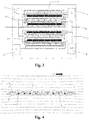
- Fig. 1 is a structural schematic diagram of a single chip bridge type magnetic field sensor disclosed by Chinese patent application CN103267955A in the prior art.
- the sensor comprises a substrate 1, sense element strings 2, reference element strings 3, shielding structures 4, electrical connecting conductors 6, and four pads 7-10 used for input/output connection and respectively used as a power supply terminal Vbias, a ground terminal GND and voltage outputs V+ and V-, wherein the sense element strings 2 and the reference element strings 3 are mutually interleaved, the sense element strings 2 are located at a gap between two shielding structures 4 and the reference element strings 3 are located below the shielding structures 4.
- a sense arm, a reference arm and pads 7-10 are connected by using the electrical connecting conductors 6.
- the sensor has the advantages of high sensitivity, good linearity, small offset and the like, but it is easily saturated, thus is applicable to magnetic fields with maximum magnetic field intensity of about 100 gausses and cannot be used for higher-intensity magnetic fields.
- Fig. 2 is a structural schematic diagram of a single chip referenced bridge type magnetic field sensor provided by the present invention.
- the sensor in Fig. 2 differs from the sensor illustrated in Fig. 1 in that: the sensor further comprises attenuators 5, the attenuators 5 and the shielding structures 4 are arranged in a spaced manner, and the number N of the attenuators 5 is not smaller than the number of rows/columns of the sense element strings 2, the number M of the shielding structures 4 is not smaller than the number of rows/columns of the reference element strings 3, wherein N ⁇ M, N and M are positive integers. In Fig. 2 , N is 5 and M is 6.
- the shapes of the attenuators 5 and the shielding structures 4 are the same and are preferably arrays of long bars which extend along a transverse/longitudinal direction, and they are composed of an identical material which is soft ferromagnetic alloy consisting of one or several elements of Ni, Fe and Co and can also be a non-ferromagnetic material but is not limited to the above-mentioned materials.
- the sense element strings 2 and the reference element strings 3 respectively consist of at least one row/column comprising one or at least two identical electrically interconnected magnetoresistive sense elements, preferably, the magnetoresistive sense elements are AMR, GMR or TMR sensor elements, the magnetoresistive sense elements included by the sense element strings 2 and the magnetoresistive sense elements included by the reference element strings 3 are the same in number, and pinning layers thereof are also the same in magnetization direction.
- the sense element strings 2 and the reference element strings 3 are mutually interleaved, each sense element string 2 and an adjacent reference element string 3 are spaced apart at a spacing L, however, for an odd number of the attenuators 5 as illustrated in Fig.
- each sense element string 2 is designed with the attenuator 5 on top of it
- each reference element string 3 is designed with the shielding structure 4 on top of it
- the sense element strings 2 and the reference element strings 3 can be respectively placed above or below the attenuators 5 and the shielding structures 4, and Fig. 2 illustrates a situation of being placed below.
- Width and area of the shielding structures 4 are greater than width and area of the attenuators 5 and are greater enough to fully cover the reference element strings 3 such that a magnetic field at the position of the reference element strings 3 can be attenuated to a very great extent and even be fully shielded, while the magnetic field which can be sensed by the sense element strings 2 is attenuated under the effect of the attenuators 5 but the attenuation amplitude is not very great, such that a gain coefficient Asns of the magnetic field at the position of the sense element strings 2 is greater than a gain coefficient Aref of the magnetic field at the position of the reference element strings 3.
- a sense arm formed by interconnected sense element strings 2 and a reference arm formed by interconnected reference element strings 3 are electrically connected to form a bridge, and input/output connecting terminals of the bridge are respectively a power supply terminal Vbias 7, a ground terminal GND 8 and voltage outputs V+ 9 and V- 10. All elements on the sensor are connected through electrical connecting conductors 6.
- the substrate 1 may also have an integrated circuit printed thereon or is connected with another substrate printed with an integrated circuit, preferably, the printed integrated circuit can be CMOS, BiCMOS (bipolar complementary metal oxide semiconductor), Bipolar, BCDMOS (bipolar-CMOS-DMOS structure) or SOI (Silicon-On-Insulator), and the reference arm and the sense arm are directly deposited on top of the integrated circuit of the substrate 1.
- CMOS complementary metal oxide semiconductor
- Bipolar bipolar complementary metal oxide semiconductor
- BCDMOS bipolar-CMOS-DMOS structure
- SOI Silicon-On-Insulator
- the substrate 1 can also be an Application-Specific Integrated Circuit (ASIC) chip comprising any one or several of an offset circuit, a gain circuit, a calibration circuit, a temperature compensation circuit and a logic circuit, wherein the logic circuit can be a digital switching circuit or a rotation angle calculating circuit but is not limited to the above-mentioned circuits.
- ASIC Application-Specific Integrated Circuit
- pads are used for input/output connection, and semiconductor package methods such as flip chip, ball grid array package, wafer level package and chip-on-board package and the like can also be adopted.
- the sensor is applicable to magnetic fields of 20-500 gausses.
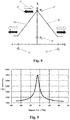
- Fig. 4 is a magnetic field distribution diagram of the sense element strings 2 and the reference element strings 3 in an externally applied magnetic field in the present invention.
- a direction of the externally applied magnetic field is 11.
- the magnetoresistive sense elements forming the sense element strings 2 and the reference element strings 3 are TMR sensor elements. From the figure, it can be seen that the magnetic field at the position of the reference element strings 3 is greatly attenuated under the effect of the shielding structures 4, while the attenuation amplitude of the magnetic field at the position of the sense element strings 2 is smaller than that of the former.
- Fig. 5 is a relation curve between positions of corresponding sense element strings 2 and reference element strings 3 in Fig. 4 and gain coefficients at corresponding positions.
- Fig. 6 is a relation curve between positions of sense element strings 2 and reference element strings 3 of a corresponding sensor structure in Fig. 1 and gain coefficients at corresponding positions.
- the numbers of the reference element strings 3 and the sense element strings 2 are the same as the numbers of those in Fig. 5 .
- the magnetic field amplitude at the position of the sense element strings 2 in the present invention is greatly attenuated, such that even though the single chip referenced bridge type magnetic field sensor in the present invention is placed in a high-intensity magnetic field, the magnetic field sensed by the sensor is the attenuated magnetic field and the sensor can still work normally as long as it is within the saturated range thereof.
- Fig. 7 is a response curve of magnetoresistive sense elements in TMR and GMR spin valve structures.
- a magnetization direction 18 of a magnetic free layer is in parallel with the direction of the externally applied magnetic field 11 and is further in parallel with the magnetization direction 19 of the pinning layers, and at this moment the magnetoresistance of the TMR elements is the smallest, i.e., R L 21.
- the magnetization direction 18 of the magnetic free layer is in parallel with the direction of the externally applied magnetic field 11 and is further in anti-parallel with the magnetization direction 19 of the pinning layers, and at this moment the magnetoresistance of the TMR elements is the largest, i.e., R H 22.
- the magnetization direction 18 of the magnetic free layer is perpendicular to the magnetization direction 19 of the pinning layers, and at this moment the magnetoresistance of the TMR elements is a median value of R L 21 and R H 22, i.e., (R L +R H )/2.
- its resistance change rate can be up to 200%, while for a GMR spin valve, its resistance change rate is only up to 10%.
- Fig. 8 is a response curve of magnetoresistive sense elements in a TMR three-layer film structure and a GMR multilayer film structure.
- the direction of the externally applied magnetic field 11 is in parallel with the magnetization direction 19 of the pinning layers and the intensity of the externally applied magnetic field is greater than -Bs 31 or Bs 32
- the magnetization direction 18 of the magnetic free layer is in parallel with the direction of the externally applied magnetic field 11 and is further in parallel with the magnetization direction 19 of the pinning layers, and at this moment the magnetoresistance of the MTJ elements is the smallest, i.e., R L 28.
- Fig. 9 is a response curve of magnetoresistive sense elements in an AMR Barber-pole structure. From the figure, it can be seen that the resistance change rate of the magnetoresistive elements is approximately 1%.
- Fig. 10 is a conversion characteristic curve of a single chip referenced bridge type sensor with magnetoresistive sense elements in a TMR spin valve structure with and without an attenuator.
- Curve 15 represents a situation that the attenuator does not exist
- curve 16 represents a situation that the attenuator is used
- a horizontal axis expresses a magnitude of an externally applied magnetic field
- a longitudinal axis expresses a ratio of sensor output voltage to power supply voltage.
- Fig. 11 is a conversion characteristic curve of a single chip referenced bridge type sensor with magnetoresistive sense elements in a TMR three-layer film structure with and without an attenuator.
- Curve 33 represents a situation that the attenuator does not exist
- curve 34 represents a situation that the attenuator is used
- a horizontal axis expresses a magnitude of an externally applied magnetic field
- a longitudinal axis expresses a ratio of sensor output voltage to power supply voltage.
Applications Claiming Priority (2)
| Application Number | Priority Date | Filing Date | Title |
|---|---|---|---|
| CN201310719255.9A CN103645449B (zh) | 2013-12-24 | 2013-12-24 | 一种用于高强度磁场的单芯片参考桥式磁传感器 |
| PCT/CN2014/094838 WO2015096744A1 (zh) | 2013-12-24 | 2014-12-24 | 一种用于高强度磁场的单芯片参考桥式磁传感器 |
Publications (3)
| Publication Number | Publication Date |
|---|---|
| EP3088908A1 EP3088908A1 (en) | 2016-11-02 |
| EP3088908A4 EP3088908A4 (en) | 2017-09-20 |
| EP3088908B1 true EP3088908B1 (en) | 2021-10-20 |
Family
ID=50250699
Family Applications (1)
| Application Number | Title | Priority Date | Filing Date |
|---|---|---|---|
| EP14874846.0A Active EP3088908B1 (en) | 2013-12-24 | 2014-12-24 | Single chip reference bridge type magnetic sensor for high-intensity magnetic field |
Country Status (5)
| Country | Link |
|---|---|
| US (1) | US10024930B2 (zh) |
| EP (1) | EP3088908B1 (zh) |
| JP (1) | JP6509231B2 (zh) |
| CN (1) | CN103645449B (zh) |
| WO (1) | WO2015096744A1 (zh) |
Families Citing this family (14)
| Publication number | Priority date | Publication date | Assignee | Title |
|---|---|---|---|---|
| CN103645449B (zh) | 2013-12-24 | 2015-11-25 | 江苏多维科技有限公司 | 一种用于高强度磁场的单芯片参考桥式磁传感器 |
| CN103954920B (zh) * | 2014-04-17 | 2016-09-14 | 江苏多维科技有限公司 | 一种单芯片三轴线性磁传感器及其制备方法 |
| CN104301851B (zh) | 2014-07-14 | 2018-01-26 | 江苏多维科技有限公司 | Tmr近场磁通信系统 |
| CN104280700B (zh) * | 2014-09-28 | 2017-09-08 | 江苏多维科技有限公司 | 一种单芯片差分自由层推挽式磁场传感器电桥及制备方法 |
| CN104698409B (zh) | 2015-02-04 | 2017-11-10 | 江苏多维科技有限公司 | 一种单芯片具有校准线圈/重置线圈的高强度磁场x轴线性磁电阻传感器 |
| CN104776794B (zh) * | 2015-04-16 | 2017-11-10 | 江苏多维科技有限公司 | 一种单封装的高强度磁场磁电阻角度传感器 |
| CN105259518A (zh) | 2015-11-03 | 2016-01-20 | 江苏多维科技有限公司 | 一种高灵敏度单芯片推挽式tmr磁场传感器 |
| CN108072850B (zh) | 2016-11-09 | 2020-06-12 | 爱盛科技股份有限公司 | 磁场感测装置 |
| CN107037382B (zh) | 2017-04-05 | 2023-05-30 | 江苏多维科技有限公司 | 一种预调制磁电阻传感器 |
| JP6996478B2 (ja) | 2018-11-16 | 2022-02-04 | Tdk株式会社 | 磁気センサ及び位置検出装置 |
| JP7006670B2 (ja) * | 2019-10-24 | 2022-01-24 | Tdk株式会社 | 磁気センサ |
| US20220326321A1 (en) | 2021-04-12 | 2022-10-13 | Jochen Schmitt | Magnetic field sensor with overcurrent detection |
| CN115236568B (zh) | 2022-09-23 | 2023-01-20 | 南方电网数字电网研究院有限公司 | 基于磁通调节器的宽量程垂直敏感磁传感器及其制备方法 |
| CN115963437B (zh) * | 2022-12-21 | 2023-10-20 | 南方电网数字电网研究院有限公司 | 多量程磁传感器、磁场测量方法及导体制备方法 |
Family Cites Families (25)
| Publication number | Priority date | Publication date | Assignee | Title |
|---|---|---|---|---|
| US3887944A (en) * | 1973-06-29 | 1975-06-03 | Ibm | Method for eliminating part of magnetic crosstalk in magnetoresistive sensors |
| JP2663460B2 (ja) * | 1987-10-09 | 1997-10-15 | 株式会社デンソー | 磁気方位センサ |
| US5217010A (en) | 1991-05-28 | 1993-06-08 | The Johns Hopkins University | Ecg amplifier and cardiac pacemaker for use during magnetic resonance imaging |
| US6185078B1 (en) * | 1998-08-21 | 2001-02-06 | International Business Machines Corporation | Spin valve read head with antiferromagnetic oxide film as longitudinal bias layer and portion of first read gap |
| US6771472B1 (en) * | 2001-12-07 | 2004-08-03 | Seagate Technology Llc | Structure to achieve thermally stable high sensitivity and linear range in bridge GMR sensor using SAF magnetic alignments |
| JP4977378B2 (ja) * | 2006-02-23 | 2012-07-18 | 山梨日本電気株式会社 | 磁気センサ、回転検出装置及び位置検出装置 |
| EP2006700B1 (en) * | 2006-04-13 | 2015-12-30 | Asahi Kasei EMD Corporation | Magnetic sensor and method for fabricating the same |
| US7639005B2 (en) * | 2007-06-15 | 2009-12-29 | Advanced Microsensors, Inc. | Giant magnetoresistive resistor and sensor apparatus and method |
| US7795862B2 (en) * | 2007-10-22 | 2010-09-14 | Allegro Microsystems, Inc. | Matching of GMR sensors in a bridge |
| JP5500785B2 (ja) | 2008-05-14 | 2014-05-21 | 新科實業有限公司 | 磁気センサ |
| JP5250109B2 (ja) * | 2009-06-12 | 2013-07-31 | アルプス・グリーンデバイス株式会社 | 磁気平衡式電流センサ |
| CN102298125B (zh) * | 2011-03-03 | 2013-01-23 | 江苏多维科技有限公司 | 推挽桥式磁电阻传感器 |
| JP5597305B2 (ja) * | 2011-03-07 | 2014-10-01 | アルプス電気株式会社 | 電流センサ |
| CN102621504B (zh) * | 2011-04-21 | 2013-09-04 | 江苏多维科技有限公司 | 单片参考全桥磁场传感器 |
| CN102323554A (zh) * | 2011-05-17 | 2012-01-18 | 杭州电子科技大学 | 集成线圈偏置的巨磁电阻磁敏传感器 |
| JP2013053903A (ja) | 2011-09-02 | 2013-03-21 | Alps Green Devices Co Ltd | 電流センサ |
| CN102565727B (zh) * | 2012-02-20 | 2016-01-20 | 江苏多维科技有限公司 | 用于测量磁场的磁电阻传感器 |
| JP2013210335A (ja) * | 2012-03-30 | 2013-10-10 | Alps Electric Co Ltd | 磁気センサ |
| CN203337808U (zh) | 2013-05-28 | 2013-12-11 | 江苏多维科技有限公司 | 单芯片桥式磁场传感器 |
| CN103267955B (zh) * | 2013-05-28 | 2016-07-27 | 江苏多维科技有限公司 | 单芯片桥式磁场传感器 |
| CN103592608B (zh) | 2013-10-21 | 2015-12-23 | 江苏多维科技有限公司 | 一种用于高强度磁场的推挽桥式磁传感器 |
| CN203587786U (zh) | 2013-10-21 | 2014-05-07 | 江苏多维科技有限公司 | 一种用于高强度磁场的推挽桥式磁传感器 |
| CN103630855B (zh) * | 2013-12-24 | 2016-04-13 | 江苏多维科技有限公司 | 一种高灵敏度推挽桥式磁传感器 |
| CN203658561U (zh) * | 2013-12-24 | 2014-06-18 | 江苏多维科技有限公司 | 一种用于高强度磁场的单芯片参考桥式磁传感器 |
| CN103645449B (zh) | 2013-12-24 | 2015-11-25 | 江苏多维科技有限公司 | 一种用于高强度磁场的单芯片参考桥式磁传感器 |
-
2013
- 2013-12-24 CN CN201310719255.9A patent/CN103645449B/zh active Active
-
2014
- 2014-12-24 US US15/108,162 patent/US10024930B2/en active Active
- 2014-12-24 WO PCT/CN2014/094838 patent/WO2015096744A1/zh active Application Filing
- 2014-12-24 JP JP2016542947A patent/JP6509231B2/ja active Active
- 2014-12-24 EP EP14874846.0A patent/EP3088908B1/en active Active
Also Published As
| Publication number | Publication date |
|---|---|
| US20160327616A1 (en) | 2016-11-10 |
| EP3088908A1 (en) | 2016-11-02 |
| CN103645449B (zh) | 2015-11-25 |
| JP2017502298A (ja) | 2017-01-19 |
| EP3088908A4 (en) | 2017-09-20 |
| US10024930B2 (en) | 2018-07-17 |
| CN103645449A (zh) | 2014-03-19 |
| WO2015096744A1 (zh) | 2015-07-02 |
| JP6509231B2 (ja) | 2019-05-08 |
Similar Documents
| Publication | Publication Date | Title |
|---|---|---|
| EP3088908B1 (en) | Single chip reference bridge type magnetic sensor for high-intensity magnetic field | |
| EP3088907B1 (en) | High-sensitivity push-pull bridge magnetic sensor | |
| EP3062119B1 (en) | Push-pull bridge-type magnetic sensor for high-intensity magnetic fields | |
| EP3006951B1 (en) | Single-chip bridge-type magnetic field sensor | |
| JP2017502298A5 (zh) | ||
| JP6420665B2 (ja) | 磁場を測定する磁気抵抗センサ | |
| US9465056B2 (en) | Current sensor with temperature-compensated magnetic tunnel junction bridge | |
| JP6193212B2 (ja) | シングルチップ2軸ブリッジ型磁界センサ | |
| EP2696209B1 (en) | Single-chip push-pull bridge-type magnetic field sensor | |
| US9702943B2 (en) | Single chip push-pull bridge-type magnetic field sensor | |
| CN202421483U (zh) | 单一芯片推挽桥式磁场传感器 | |
| EP2696211A1 (en) | Single chip bridge magnetic field sensor and preparation method thereof | |
| CN203658561U (zh) | 一种用于高强度磁场的单芯片参考桥式磁传感器 | |
| CN203337808U (zh) | 单芯片桥式磁场传感器 | |
| CN203587786U (zh) | 一种用于高强度磁场的推挽桥式磁传感器 |
Legal Events
| Date | Code | Title | Description |
|---|---|---|---|
| PUAI | Public reference made under article 153(3) epc to a published international application that has entered the european phase |
Free format text: ORIGINAL CODE: 0009012 |
|
| STAA | Information on the status of an ep patent application or granted ep patent |
Free format text: STATUS: REQUEST FOR EXAMINATION WAS MADE |
|
| 17P | Request for examination filed |
Effective date: 20160708 |
|
| AK | Designated contracting states |
Kind code of ref document: A1 Designated state(s): AL AT BE BG CH CY CZ DE DK EE ES FI FR GB GR HR HU IE IS IT LI LT LU LV MC MK MT NL NO PL PT RO RS SE SI SK SM TR |
|
| AX | Request for extension of the european patent |
Extension state: BA ME |
|
| DAX | Request for extension of the european patent (deleted) | ||
| A4 | Supplementary search report drawn up and despatched |
Effective date: 20170818 |
|
| RIC1 | Information provided on ipc code assigned before grant |
Ipc: G01R 33/09 20060101AFI20170811BHEP |
|
| GRAP | Despatch of communication of intention to grant a patent |
Free format text: ORIGINAL CODE: EPIDOSNIGR1 |
|
| STAA | Information on the status of an ep patent application or granted ep patent |
Free format text: STATUS: GRANT OF PATENT IS INTENDED |
|
| INTG | Intention to grant announced |
Effective date: 20210512 |
|
| GRAS | Grant fee paid |
Free format text: ORIGINAL CODE: EPIDOSNIGR3 |
|
| GRAA | (expected) grant |
Free format text: ORIGINAL CODE: 0009210 |
|
| STAA | Information on the status of an ep patent application or granted ep patent |
Free format text: STATUS: THE PATENT HAS BEEN GRANTED |
|
| AK | Designated contracting states |
Kind code of ref document: B1 Designated state(s): AL AT BE BG CH CY CZ DE DK EE ES FI FR GB GR HR HU IE IS IT LI LT LU LV MC MK MT NL NO PL PT RO RS SE SI SK SM TR |
|
| REG | Reference to a national code |
Ref country code: GB Ref legal event code: FG4D |
|
| REG | Reference to a national code |
Ref country code: CH Ref legal event code: EP |
|
| REG | Reference to a national code |
Ref country code: IE Ref legal event code: FG4D |
|
| REG | Reference to a national code |
Ref country code: DE Ref legal event code: R096 Ref document number: 602014080817 Country of ref document: DE |
|
| REG | Reference to a national code |
Ref country code: AT Ref legal event code: REF Ref document number: 1440383 Country of ref document: AT Kind code of ref document: T Effective date: 20211115 |
|
| REG | Reference to a national code |
Ref country code: LT Ref legal event code: MG9D |
|
| REG | Reference to a national code |
Ref country code: NL Ref legal event code: MP Effective date: 20211020 |
|
| REG | Reference to a national code |
Ref country code: AT Ref legal event code: MK05 Ref document number: 1440383 Country of ref document: AT Kind code of ref document: T Effective date: 20211020 |
|
| PG25 | Lapsed in a contracting state [announced via postgrant information from national office to epo] |
Ref country code: RS Free format text: LAPSE BECAUSE OF FAILURE TO SUBMIT A TRANSLATION OF THE DESCRIPTION OR TO PAY THE FEE WITHIN THE PRESCRIBED TIME-LIMIT Effective date: 20211020 Ref country code: LT Free format text: LAPSE BECAUSE OF FAILURE TO SUBMIT A TRANSLATION OF THE DESCRIPTION OR TO PAY THE FEE WITHIN THE PRESCRIBED TIME-LIMIT Effective date: 20211020 Ref country code: FI Free format text: LAPSE BECAUSE OF FAILURE TO SUBMIT A TRANSLATION OF THE DESCRIPTION OR TO PAY THE FEE WITHIN THE PRESCRIBED TIME-LIMIT Effective date: 20211020 Ref country code: BG Free format text: LAPSE BECAUSE OF FAILURE TO SUBMIT A TRANSLATION OF THE DESCRIPTION OR TO PAY THE FEE WITHIN THE PRESCRIBED TIME-LIMIT Effective date: 20220120 Ref country code: AT Free format text: LAPSE BECAUSE OF FAILURE TO SUBMIT A TRANSLATION OF THE DESCRIPTION OR TO PAY THE FEE WITHIN THE PRESCRIBED TIME-LIMIT Effective date: 20211020 |
|
| RAP4 | Party data changed (patent owner data changed or rights of a patent transferred) |
Owner name: MULTIDIMENSION TECHNOLOGY CO., LTD. |
|
| PG25 | Lapsed in a contracting state [announced via postgrant information from national office to epo] |
Ref country code: IS Free format text: LAPSE BECAUSE OF FAILURE TO SUBMIT A TRANSLATION OF THE DESCRIPTION OR TO PAY THE FEE WITHIN THE PRESCRIBED TIME-LIMIT Effective date: 20220220 Ref country code: SE Free format text: LAPSE BECAUSE OF FAILURE TO SUBMIT A TRANSLATION OF THE DESCRIPTION OR TO PAY THE FEE WITHIN THE PRESCRIBED TIME-LIMIT Effective date: 20211020 Ref country code: PT Free format text: LAPSE BECAUSE OF FAILURE TO SUBMIT A TRANSLATION OF THE DESCRIPTION OR TO PAY THE FEE WITHIN THE PRESCRIBED TIME-LIMIT Effective date: 20220221 Ref country code: PL Free format text: LAPSE BECAUSE OF FAILURE TO SUBMIT A TRANSLATION OF THE DESCRIPTION OR TO PAY THE FEE WITHIN THE PRESCRIBED TIME-LIMIT Effective date: 20211020 Ref country code: NO Free format text: LAPSE BECAUSE OF FAILURE TO SUBMIT A TRANSLATION OF THE DESCRIPTION OR TO PAY THE FEE WITHIN THE PRESCRIBED TIME-LIMIT Effective date: 20220120 Ref country code: NL Free format text: LAPSE BECAUSE OF FAILURE TO SUBMIT A TRANSLATION OF THE DESCRIPTION OR TO PAY THE FEE WITHIN THE PRESCRIBED TIME-LIMIT Effective date: 20211020 Ref country code: LV Free format text: LAPSE BECAUSE OF FAILURE TO SUBMIT A TRANSLATION OF THE DESCRIPTION OR TO PAY THE FEE WITHIN THE PRESCRIBED TIME-LIMIT Effective date: 20211020 Ref country code: HR Free format text: LAPSE BECAUSE OF FAILURE TO SUBMIT A TRANSLATION OF THE DESCRIPTION OR TO PAY THE FEE WITHIN THE PRESCRIBED TIME-LIMIT Effective date: 20211020 Ref country code: GR Free format text: LAPSE BECAUSE OF FAILURE TO SUBMIT A TRANSLATION OF THE DESCRIPTION OR TO PAY THE FEE WITHIN THE PRESCRIBED TIME-LIMIT Effective date: 20220121 Ref country code: ES Free format text: LAPSE BECAUSE OF FAILURE TO SUBMIT A TRANSLATION OF THE DESCRIPTION OR TO PAY THE FEE WITHIN THE PRESCRIBED TIME-LIMIT Effective date: 20211020 |
|
| REG | Reference to a national code |
Ref country code: CH Ref legal event code: PK Free format text: BERICHTIGUNGEN |
|
| RIN2 | Information on inventor provided after grant (corrected) |
Inventor name: DEAK, JAMES GEZA |
|
| REG | Reference to a national code |
Ref country code: DE Ref legal event code: R097 Ref document number: 602014080817 Country of ref document: DE |
|
| PG25 | Lapsed in a contracting state [announced via postgrant information from national office to epo] |
Ref country code: SM Free format text: LAPSE BECAUSE OF FAILURE TO SUBMIT A TRANSLATION OF THE DESCRIPTION OR TO PAY THE FEE WITHIN THE PRESCRIBED TIME-LIMIT Effective date: 20211020 Ref country code: SK Free format text: LAPSE BECAUSE OF FAILURE TO SUBMIT A TRANSLATION OF THE DESCRIPTION OR TO PAY THE FEE WITHIN THE PRESCRIBED TIME-LIMIT Effective date: 20211020 Ref country code: RO Free format text: LAPSE BECAUSE OF FAILURE TO SUBMIT A TRANSLATION OF THE DESCRIPTION OR TO PAY THE FEE WITHIN THE PRESCRIBED TIME-LIMIT Effective date: 20211020 Ref country code: MC Free format text: LAPSE BECAUSE OF FAILURE TO SUBMIT A TRANSLATION OF THE DESCRIPTION OR TO PAY THE FEE WITHIN THE PRESCRIBED TIME-LIMIT Effective date: 20211020 Ref country code: EE Free format text: LAPSE BECAUSE OF FAILURE TO SUBMIT A TRANSLATION OF THE DESCRIPTION OR TO PAY THE FEE WITHIN THE PRESCRIBED TIME-LIMIT Effective date: 20211020 Ref country code: DK Free format text: LAPSE BECAUSE OF FAILURE TO SUBMIT A TRANSLATION OF THE DESCRIPTION OR TO PAY THE FEE WITHIN THE PRESCRIBED TIME-LIMIT Effective date: 20211020 Ref country code: CZ Free format text: LAPSE BECAUSE OF FAILURE TO SUBMIT A TRANSLATION OF THE DESCRIPTION OR TO PAY THE FEE WITHIN THE PRESCRIBED TIME-LIMIT Effective date: 20211020 |
|
| REG | Reference to a national code |
Ref country code: CH Ref legal event code: PL |
|
| PLBE | No opposition filed within time limit |
Free format text: ORIGINAL CODE: 0009261 |
|
| STAA | Information on the status of an ep patent application or granted ep patent |
Free format text: STATUS: NO OPPOSITION FILED WITHIN TIME LIMIT |
|
| REG | Reference to a national code |
Ref country code: BE Ref legal event code: MM Effective date: 20211231 |
|
| 26N | No opposition filed |
Effective date: 20220721 |
|
| PG25 | Lapsed in a contracting state [announced via postgrant information from national office to epo] |
Ref country code: LU Free format text: LAPSE BECAUSE OF NON-PAYMENT OF DUE FEES Effective date: 20211224 Ref country code: IE Free format text: LAPSE BECAUSE OF NON-PAYMENT OF DUE FEES Effective date: 20211224 Ref country code: AL Free format text: LAPSE BECAUSE OF FAILURE TO SUBMIT A TRANSLATION OF THE DESCRIPTION OR TO PAY THE FEE WITHIN THE PRESCRIBED TIME-LIMIT Effective date: 20211020 |
|
| PG25 | Lapsed in a contracting state [announced via postgrant information from national office to epo] |
Ref country code: SI Free format text: LAPSE BECAUSE OF FAILURE TO SUBMIT A TRANSLATION OF THE DESCRIPTION OR TO PAY THE FEE WITHIN THE PRESCRIBED TIME-LIMIT Effective date: 20211020 Ref country code: BE Free format text: LAPSE BECAUSE OF NON-PAYMENT OF DUE FEES Effective date: 20211231 |
|
| PG25 | Lapsed in a contracting state [announced via postgrant information from national office to epo] |
Ref country code: LI Free format text: LAPSE BECAUSE OF NON-PAYMENT OF DUE FEES Effective date: 20211231 Ref country code: CH Free format text: LAPSE BECAUSE OF NON-PAYMENT OF DUE FEES Effective date: 20211231 |
|
| PG25 | Lapsed in a contracting state [announced via postgrant information from national office to epo] |
Ref country code: IT Free format text: LAPSE BECAUSE OF FAILURE TO SUBMIT A TRANSLATION OF THE DESCRIPTION OR TO PAY THE FEE WITHIN THE PRESCRIBED TIME-LIMIT Effective date: 20211020 Ref country code: HU Free format text: LAPSE BECAUSE OF FAILURE TO SUBMIT A TRANSLATION OF THE DESCRIPTION OR TO PAY THE FEE WITHIN THE PRESCRIBED TIME-LIMIT; INVALID AB INITIO Effective date: 20141224 |
|
| PGFP | Annual fee paid to national office [announced via postgrant information from national office to epo] |
Ref country code: DE Payment date: 20221228 Year of fee payment: 9 |
|
| PG25 | Lapsed in a contracting state [announced via postgrant information from national office to epo] |
Ref country code: CY Free format text: LAPSE BECAUSE OF FAILURE TO SUBMIT A TRANSLATION OF THE DESCRIPTION OR TO PAY THE FEE WITHIN THE PRESCRIBED TIME-LIMIT Effective date: 20211020 |
|
| P01 | Opt-out of the competence of the unified patent court (upc) registered |
Effective date: 20230626 |
|
| PGFP | Annual fee paid to national office [announced via postgrant information from national office to epo] |
Ref country code: GB Payment date: 20231227 Year of fee payment: 10 |
|
| PGFP | Annual fee paid to national office [announced via postgrant information from national office to epo] |
Ref country code: FR Payment date: 20231227 Year of fee payment: 10 |
|
| PG25 | Lapsed in a contracting state [announced via postgrant information from national office to epo] |
Ref country code: MK Free format text: LAPSE BECAUSE OF FAILURE TO SUBMIT A TRANSLATION OF THE DESCRIPTION OR TO PAY THE FEE WITHIN THE PRESCRIBED TIME-LIMIT Effective date: 20211020 |
|
| PGFP | Annual fee paid to national office [announced via postgrant information from national office to epo] |
Ref country code: DE Payment date: 20231229 Year of fee payment: 10 |