EP3086460A2 - Triboelectric generator - Google Patents
Triboelectric generator Download PDFInfo
- Publication number
- EP3086460A2 EP3086460A2 EP16163889.5A EP16163889A EP3086460A2 EP 3086460 A2 EP3086460 A2 EP 3086460A2 EP 16163889 A EP16163889 A EP 16163889A EP 3086460 A2 EP3086460 A2 EP 3086460A2
- Authority
- EP
- European Patent Office
- Prior art keywords
- electrode
- energy generation
- generation layer
- triboelectric generator
- substrate
- Prior art date
- Legal status (The legal status is an assumption and is not a legal conclusion. Google has not performed a legal analysis and makes no representation as to the accuracy of the status listed.)
- Granted
Links
- 239000000463 material Substances 0.000 claims abstract description 113
- 239000013078 crystal Substances 0.000 claims abstract description 11
- 239000010410 layer Substances 0.000 claims description 165
- 239000000758 substrate Substances 0.000 claims description 121
- OKTJSMMVPCPJKN-UHFFFAOYSA-N Carbon Chemical compound [C] OKTJSMMVPCPJKN-UHFFFAOYSA-N 0.000 claims description 45
- 239000004205 dimethyl polysiloxane Substances 0.000 claims description 34
- 229920000435 poly(dimethylsiloxane) Polymers 0.000 claims description 34
- 229910021389 graphene Inorganic materials 0.000 claims description 27
- 239000002041 carbon nanotube Substances 0.000 claims description 18
- 229910021393 carbon nanotube Inorganic materials 0.000 claims description 18
- 239000004642 Polyimide Substances 0.000 claims description 14
- 229920001721 polyimide Polymers 0.000 claims description 14
- 229910052751 metal Inorganic materials 0.000 claims description 13
- 239000002184 metal Substances 0.000 claims description 13
- -1 polydimethylsiloxane Polymers 0.000 claims description 11
- 229910052723 transition metal Inorganic materials 0.000 claims description 9
- 150000003624 transition metals Chemical class 0.000 claims description 9
- 229910052711 selenium Inorganic materials 0.000 claims description 7
- 229910052717 sulfur Inorganic materials 0.000 claims description 7
- JOYRKODLDBILNP-UHFFFAOYSA-N Ethyl urethane Chemical compound CCOC(N)=O JOYRKODLDBILNP-UHFFFAOYSA-N 0.000 claims description 6
- 239000004677 Nylon Substances 0.000 claims description 6
- 239000004809 Teflon Substances 0.000 claims description 6
- 229920006362 Teflon® Polymers 0.000 claims description 6
- 229910052733 gallium Inorganic materials 0.000 claims description 6
- 229910052732 germanium Inorganic materials 0.000 claims description 6
- 229910052735 hafnium Inorganic materials 0.000 claims description 6
- 229910052738 indium Inorganic materials 0.000 claims description 6
- 229910052750 molybdenum Inorganic materials 0.000 claims description 6
- 229910052758 niobium Inorganic materials 0.000 claims description 6
- 229920001778 nylon Polymers 0.000 claims description 6
- 229910052715 tantalum Inorganic materials 0.000 claims description 6
- 229910052713 technetium Inorganic materials 0.000 claims description 6
- 229910052718 tin Inorganic materials 0.000 claims description 6
- 229910052719 titanium Inorganic materials 0.000 claims description 6
- 229910052721 tungsten Inorganic materials 0.000 claims description 6
- 229910052720 vanadium Inorganic materials 0.000 claims description 6
- 229910052726 zirconium Inorganic materials 0.000 claims description 6
- 239000002070 nanowire Substances 0.000 claims description 5
- 229910052702 rhenium Inorganic materials 0.000 claims description 5
- 229910052714 tellurium Inorganic materials 0.000 claims description 5
- 229910052802 copper Inorganic materials 0.000 claims description 4
- 229910052745 lead Inorganic materials 0.000 claims description 4
- 239000002356 single layer Substances 0.000 claims description 4
- 125000006850 spacer group Chemical group 0.000 claims description 4
- 229910052582 BN Inorganic materials 0.000 claims description 3
- 235000013870 dimethyl polysiloxane Nutrition 0.000 description 32
- 229910052961 molybdenite Inorganic materials 0.000 description 28
- CWQXQMHSOZUFJS-UHFFFAOYSA-N molybdenum disulfide Chemical compound S=[Mo]=S CWQXQMHSOZUFJS-UHFFFAOYSA-N 0.000 description 28
- 229910052982 molybdenum disulfide Inorganic materials 0.000 description 28
- 239000002019 doping agent Substances 0.000 description 22
- 239000002086 nanomaterial Substances 0.000 description 20
- 238000000034 method Methods 0.000 description 11
- 229910052798 chalcogen Inorganic materials 0.000 description 7
- 150000001787 chalcogens Chemical class 0.000 description 7
- 238000005259 measurement Methods 0.000 description 7
- 229920001343 polytetrafluoroethylene Polymers 0.000 description 7
- 239000004810 polytetrafluoroethylene Substances 0.000 description 7
- 229940058401 polytetrafluoroethylene Drugs 0.000 description 7
- 239000005020 polyethylene terephthalate Substances 0.000 description 5
- 229920000139 polyethylene terephthalate Polymers 0.000 description 5
- 150000001875 compounds Chemical class 0.000 description 4
- 238000004519 manufacturing process Methods 0.000 description 4
- 239000004417 polycarbonate Substances 0.000 description 4
- 229920000515 polycarbonate Polymers 0.000 description 4
- 238000005452 bending Methods 0.000 description 3
- 230000008602 contraction Effects 0.000 description 3
- 230000005611 electricity Effects 0.000 description 3
- 238000002513 implantation Methods 0.000 description 3
- 229930027945 nicotinamide-adenine dinucleotide Natural products 0.000 description 3
- 229920003229 poly(methyl methacrylate) Polymers 0.000 description 3
- 239000004926 polymethyl methacrylate Substances 0.000 description 3
- 238000003825 pressing Methods 0.000 description 3
- SQGYOTSLMSWVJD-UHFFFAOYSA-N silver(1+) nitrate Chemical compound [Ag+].[O-]N(=O)=O SQGYOTSLMSWVJD-UHFFFAOYSA-N 0.000 description 3
- HZNVUJQVZSTENZ-UHFFFAOYSA-N 2,3-dichloro-5,6-dicyano-1,4-benzoquinone Chemical compound ClC1=C(Cl)C(=O)C(C#N)=C(C#N)C1=O HZNVUJQVZSTENZ-UHFFFAOYSA-N 0.000 description 2
- QTBSBXVTEAMEQO-UHFFFAOYSA-N Acetic acid Chemical compound CC(O)=O QTBSBXVTEAMEQO-UHFFFAOYSA-N 0.000 description 2
- BAWFJGJZGIEFAR-NNYOXOHSSA-N NAD zwitterion Chemical compound NC(=O)C1=CC=C[N+]([C@H]2[C@@H]([C@H](O)[C@@H](COP([O-])(=O)OP(O)(=O)OC[C@@H]3[C@H]([C@@H](O)[C@@H](O3)N3C4=NC=NC(N)=C4N=C3)O)O2)O)=C1 BAWFJGJZGIEFAR-NNYOXOHSSA-N 0.000 description 2
- DFPAKSUCGFBDDF-UHFFFAOYSA-N Nicotinamide Chemical compound NC(=O)C1=CC=CN=C1 DFPAKSUCGFBDDF-UHFFFAOYSA-N 0.000 description 2
- 229920002873 Polyethylenimine Polymers 0.000 description 2
- JUJWROOIHBZHMG-UHFFFAOYSA-N Pyridine Chemical group C1=CC=NC=C1 JUJWROOIHBZHMG-UHFFFAOYSA-N 0.000 description 2
- XUIMIQQOPSSXEZ-UHFFFAOYSA-N Silicon Chemical compound [Si] XUIMIQQOPSSXEZ-UHFFFAOYSA-N 0.000 description 2
- DFPAKSUCGFBDDF-ZQBYOMGUSA-N [14c]-nicotinamide Chemical class N[14C](=O)C1=CC=CN=C1 DFPAKSUCGFBDDF-ZQBYOMGUSA-N 0.000 description 2
- LYBDVVBIMGTZMB-HVIJGSDCSA-N [3-[hydroxy-[(2s,3r,5s,6s)-2,3,4,5,6-pentahydroxycyclohexyl]oxyphosphoryl]oxy-2-tetradecanoyloxypropyl] tetradecanoate Chemical compound CCCCCCCCCCCCCC(=O)OCC(OC(=O)CCCCCCCCCCCCC)COP(O)(=O)OC1[C@@H](O)[C@@H](O)C(O)[C@@H](O)[C@@H]1O LYBDVVBIMGTZMB-HVIJGSDCSA-N 0.000 description 2
- 239000004020 conductor Substances 0.000 description 2
- 230000007423 decrease Effects 0.000 description 2
- 239000004744 fabric Substances 0.000 description 2
- 239000000835 fiber Substances 0.000 description 2
- 230000014509 gene expression Effects 0.000 description 2
- 239000011521 glass Substances 0.000 description 2
- 229950006238 nadide Drugs 0.000 description 2
- 229910052710 silicon Inorganic materials 0.000 description 2
- 239000010703 silicon Substances 0.000 description 2
- 229910005543 GaSe Inorganic materials 0.000 description 1
- 229910005866 GeSe Inorganic materials 0.000 description 1
- 229910003803 Gold(III) chloride Inorganic materials 0.000 description 1
- 229910004042 HAuCl4 Inorganic materials 0.000 description 1
- 229910016021 MoTe2 Inorganic materials 0.000 description 1
- 229910004069 NO2BF4 Inorganic materials 0.000 description 1
- 229910000910 NO2SbF6 Inorganic materials 0.000 description 1
- 229910004064 NOBF4 Inorganic materials 0.000 description 1
- 229910020039 NbSe2 Inorganic materials 0.000 description 1
- GRYLNZFGIOXLOG-UHFFFAOYSA-N Nitric acid Chemical compound O[N+]([O-])=O GRYLNZFGIOXLOG-UHFFFAOYSA-N 0.000 description 1
- QAOWNCQODCNURD-UHFFFAOYSA-N Sulfuric acid Chemical compound OS(O)(=O)=O QAOWNCQODCNURD-UHFFFAOYSA-N 0.000 description 1
- 238000005411 Van der Waals force Methods 0.000 description 1
- 229910003090 WSe2 Inorganic materials 0.000 description 1
- 229910006247 ZrS2 Inorganic materials 0.000 description 1
- XJLXINKUBYWONI-DQQFMEOOSA-N [[(2r,3r,4r,5r)-5-(6-aminopurin-9-yl)-3-hydroxy-4-phosphonooxyoxolan-2-yl]methoxy-hydroxyphosphoryl] [(2s,3r,4s,5s)-5-(3-carbamoylpyridin-1-ium-1-yl)-3,4-dihydroxyoxolan-2-yl]methyl phosphate Chemical compound NC(=O)C1=CC=C[N+]([C@@H]2[C@H]([C@@H](O)[C@H](COP([O-])(=O)OP(O)(=O)OC[C@@H]3[C@H]([C@@H](OP(O)(O)=O)[C@@H](O3)N3C4=NC=NC(N)=C4N=C3)O)O2)O)=C1 XJLXINKUBYWONI-DQQFMEOOSA-N 0.000 description 1
- 150000007513 acids Chemical class 0.000 description 1
- 229910052783 alkali metal Inorganic materials 0.000 description 1
- 150000001340 alkali metals Chemical class 0.000 description 1
- 125000004432 carbon atom Chemical group C* 0.000 description 1
- 150000004770 chalcogenides Chemical class 0.000 description 1
- CZKMPDNXOGQMFW-UHFFFAOYSA-N chloro(triethyl)germane Chemical compound CC[Ge](Cl)(CC)CC CZKMPDNXOGQMFW-UHFFFAOYSA-N 0.000 description 1
- LEKPFOXEZRZPGW-UHFFFAOYSA-N copper;dicyanide Chemical compound [Cu+2].N#[C-].N#[C-] LEKPFOXEZRZPGW-UHFFFAOYSA-N 0.000 description 1
- 239000007789 gas Substances 0.000 description 1
- RJHLTVSLYWWTEF-UHFFFAOYSA-K gold trichloride Chemical compound Cl[Au](Cl)Cl RJHLTVSLYWWTEF-UHFFFAOYSA-K 0.000 description 1
- 238000003306 harvesting Methods 0.000 description 1
- 239000007943 implant Substances 0.000 description 1
- 239000011810 insulating material Substances 0.000 description 1
- 238000005468 ion implantation Methods 0.000 description 1
- 239000002608 ionic liquid Substances 0.000 description 1
- 238000006138 lithiation reaction Methods 0.000 description 1
- 229910052744 lithium Inorganic materials 0.000 description 1
- 229960003966 nicotinamide Drugs 0.000 description 1
- 235000005152 nicotinamide Nutrition 0.000 description 1
- 239000011570 nicotinamide Substances 0.000 description 1
- BOPGDPNILDQYTO-NNYOXOHSSA-N nicotinamide-adenine dinucleotide Chemical compound C1=CCC(C(=O)N)=CN1[C@H]1[C@H](O)[C@H](O)[C@@H](COP(O)(=O)OP(O)(=O)OC[C@@H]2[C@H]([C@@H](O)[C@@H](O2)N2C3=NC=NC(N)=C3N=C2)O)O1 BOPGDPNILDQYTO-NNYOXOHSSA-N 0.000 description 1
- 229910017604 nitric acid Inorganic materials 0.000 description 1
- 229910052757 nitrogen Inorganic materials 0.000 description 1
- 125000004433 nitrogen atom Chemical group N* 0.000 description 1
- 150000002894 organic compounds Chemical class 0.000 description 1
- YJVFFLUZDVXJQI-UHFFFAOYSA-L palladium(ii) acetate Chemical compound [Pd+2].CC([O-])=O.CC([O-])=O YJVFFLUZDVXJQI-UHFFFAOYSA-L 0.000 description 1
- 229920000642 polymer Polymers 0.000 description 1
- 229910052700 potassium Inorganic materials 0.000 description 1
- 239000004065 semiconductor Substances 0.000 description 1
- 238000000926 separation method Methods 0.000 description 1
- QRUBYZBWAOOHSV-UHFFFAOYSA-M silver trifluoromethanesulfonate Chemical compound [Ag+].[O-]S(=O)(=O)C(F)(F)F QRUBYZBWAOOHSV-UHFFFAOYSA-M 0.000 description 1
- 239000000126 substance Substances 0.000 description 1
Images


Classifications
-
- H—ELECTRICITY
- H02—GENERATION; CONVERSION OR DISTRIBUTION OF ELECTRIC POWER
- H02N—ELECTRIC MACHINES NOT OTHERWISE PROVIDED FOR
- H02N1/00—Electrostatic generators or motors using a solid moving electrostatic charge carrier
- H02N1/04—Friction generators
Abstract

Description
- Example embodiments relate to a triboelectric generator, and more particularly, to a triboelectric generator using a one-dimensional nanomaterial or a two-dimensional material.
- Energy harvesting devices are new eco-friendly energy generating devices that may extract energy by converting mechanical energy generated from wind, vibrations, or movements of a person with respect to a surrounding environment to electric energy.
- Example embodiments relate to a triboelectric generator using a one-dimensional nanomaterial or a two-dimensional material.
- Additional example embodiments will be set forth in part in the description which follows and, in part, will be apparent from the description, or may be learned by practice of the example embodiments.
- According to a first aspect of the invention, there is provided a triboelectric generator includes first and second electrodes provided to face each other, and a first energy generation layer provided on the first electrode and generating electric energy through contact with other material, the first energy generation layer including a two-dimensional (2D) material having a crystal structure of a 2D shape.
- The two-dimensional material may include at least one of hexagonal-boron nitride (h-BN) and transition metal dichalcogenide (TMD). The TMD may include one metal element from Mo, W, Nb, V, Ta, Ti, Zr, Hf, Tc, Re, Cu, Ga, In, Sn, Ge, and Pb and one chalcogen element from S, Se, and Te.
- The 2D material may have a single layer or a multilayer structure. The 2D material may have a thickness of about 0.3 nm to about 1000 nm.
- The 2D material may be doped or undoped. The triboelectric generator may further include a spacer provided between the first electrode and the second electrode.
- The first energy layer may generate electric energy through contact with the second electrode.
- The triboelectric generator may further include at least one of a first substrate on which the first electrode and the first energy generation layer are provided and a second substrate on which the second electrode is provided. The first energy generation layer may generate electric energy through contact with the second electrode or the second substrate.
- At least one of the first and second substrates may be stretchable. At least one of the first and second substrates may include at least one of polydimethylsiloxane (PDMS), polyimide (PI), Teflon, urethane, and nylon. At least one of the first and second substrates may have an elongation percentage of about 200% or low.
- At least one of the first and second substrates may have a surface having a shape of a wavy pattern. The first electrode and the first energy generation layer may have a shape corresponding to a surface of the first substrate and the second electrode may have a shape corresponding to a surface of the second substrate.
- At least one of the first and second electrodes may include at least one of carbon nanotube (CNT), graphene, Ag nanowire, metal, and metal mesh.
- The triboelectric generator may further include a second energy generation layer provided on the second electrode and generating electric energy through contact with the first energy generation layer. The triboelectric generator may further include at least one of a first substrate on which the first electrode and the first energy generation layer are provided, and a second substrate on which the second electrode and the second energy generation layer are provided. At least one of the first and second substrates may be stretchable.
- According to another example embodiment, a triboelectric generator includes first and second electrodes provided to face each other and having stretchability, and a first energy generation layer provided on the first electrode and generating electric energy through contact with another material or other materials.
- The first energy generation layer may include at least one of one-dimensional (1 D) material having a 1 D shape of a nano size and a two-dimensional (2D) material having a crystal structure of a 2D shape. The 1 D nanomaterial may include CNT and the 2D material includes at least one of graphene, h-BN, and TMD.
- The first energy generation layer may generate electric energy through contact with the second electrode.
- The triboelectric generator may further include at least one of a first substrate that is stretchable, on which the first electrode and the first energy generation layer are provided, and a second substrate that is stretchable, on which the second electrode is provided.
- The first energy generation layer may generate electric energy through contact with the second electrode or the second substrate.
- At least one of the first and second substrates may have a surface having a shape of a wavy pattern.
- The first electrode and the first energy generation layer may have a shape corresponding to a surface of the first substrate, and the second electrode has a shape corresponding to a surface of the second substrate.
- The triboelectric generator may further include a second energy generation layer provided on the second electrode and generating electric energy through contact with the first energy generation layer.
- The triboelectric generator may further include at least one of a first substrate that is stretchable, on which the first electrode and the first energy generation layer are provided, and a second substrate that is stretchable, on which the second electrode and the second energy generation layer are provided.
- According to another example embodiment, a triboelectric generator includes a plurality of energy generation units that are stacked on top of each other, wherein each of, or one or more of, the energy generation units includes first and second electrodes provided to face each other, and a first energy generation layer provided on the first electrode and generating electric energy through contact with other material, the first energy generation layer including a 2D material having a crystal structure of a 2D shape.
- The 2D material may include at least one of graphene, h-BN, and TMD.
- The triboelectric generator may further include a second energy generation layer provided on the second electrode and generating electric energy through contact with the first energy generation layer.
- The energy generation units may be serially connected to one another.
- According to another example embodiment, a triboelectric generator includes a plurality of energy generation units that are stacked on top of each other, wherein each of, or one or more of, the energy generation units includes first and second electrodes provided to face each other and having stretchability, and a first energy generation layer provided on the first electrode and generating electric energy through contact with other material.
- The first energy generation layer may include at least one of a 1 D material having a 1 D shape of a nano size and a 2D material having a crystal structure of a 2D shape. The 1 D nanomaterial may include CNT and the 2D material includes at least one of graphene, h-BN, and TMD.
- The triboelectric generator may further include a second energy generation layer provided on the second electrode and generating electric energy through contact with the first energy generation layer.
- These and/or other example embodiments will become apparent and more readily appreciated from the following description, taken in conjunction with the accompanying drawings in which:
-
FIG. 1 is a cross-sectional view of a triboelectric generator according to an example embodiment; -
FIGS. 2A to 2E illustrate an operation of the triboelectric generator illustrated inFIG. 1 to generate electric energy by pressing or bending; -
FIGS. 3A to 3D illustrate an operation of the triboelectric generator illustrated inFIG. 1 to generate electric energy by sliding; -
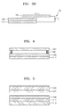
FIG. 4 is a cross-sectional view of a triboelectric generator according to another example embodiment -
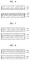
FIG. 5 is a cross-sectional view of a triboelectric generator according to another example embodiment -
FIG. 6 is a cross-sectional view of a triboelectric generator according to another example embodiment -
FIG. 7 is a cross-sectional view of a triboelectric generator according to another example embodiment -
FIG. 8 is a cross-sectional view of a triboelectric generator according to another example embodiment -
FIG. 9 is a cross-sectional view of a triboelectric generator according to another example embodiment -
FIG. 10 illustrates a triboelectric generator according to another example embodiment; -
FIG. 11 illustrates output voltages according to a thickness of an energy generation layer formed of or include a two-dimensional material in a triboelectric generator according to an example embodiment; -
FIG. 12 illustrates output current densities according to a thickness of an energy generation layer formed of or include a two-dimensional material in a triboelectric generator according to an example embodiment; -
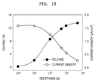
FIG. 13 illustrates an output voltage and an output current density according to resistance of a measurement circuit, in a triboelectric generator according to an example embodiment; -
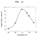
FIG. 14 illustrates an output power density according to resistance of a measurement circuit, in a triboelectric generator according to an example embodiment; -
FIG. 15 illustrates charging characteristics of a MoS2 material; -
FIG. 16 illustrates charging characteristics of a WS2 material; -
FIGS. 17A and 17B illustrate a method of manufacturing a triboelectric generator including graphene having a wavy pattern by using stretchability of a polydimethylsiloxane (PDMS) substrate; and -
FIGS. 18A to 18C illustrate output voltages according to an elongation percentage of PDMS, in a triboelectric generator manufactured by the example method ofFIGS. 17A and 17B . - Reference will now be made in detail to example embodiments illustrated in the accompanying drawings, wherein like reference numerals refer to like elements throughout. The thickness or size of each layer illustrated in the drawings may be exaggerated for convenience of explanation and clarity. Also, in the following description, when a layer is described to exist on another layer, the layer may exist directly on the other layer or a third layer may be interposed therebetween. Since a material forming each layer in the following example embodiments is an example, other materials may be used therefor. As used herein, the term "and/or" includes any and all combinations of one or more of the associated listed items. Expressions such as "at least one of," when preceding a list of elements, modify the entire list of elements and do not modify the individual elements of the list.
- It will be understood that when an element is referred to as being "on," "connected" or "coupled" to another element, it can be directly on, connected or coupled to the other element or intervening elements may be present. In contrast, when an element is referred to as being "directly on," "directly connected" or "directly coupled" to another element, there are no intervening elements present. Further, it will be understood that when a layer is referred to as being "under" another layer, it can be directly under or one or more intervening layers may also be present. In addition, it will also be understood that when a layer is referred to as being "between" two layers, it can be the only layer between the two layers, or one or more intervening layers may also be present.
- It will be understood that, although the terms "first", "second", etc. may be used herein to describe various elements, components, regions, layers and/or sections, these elements, components, regions, layers and/or sections should not be limited by these terms. These terms are only used to distinguish one element, component, region, layer or section from another element, component, region, layer or section. Thus, a first element, component, region, layer or section discussed below could be termed a second element, component, region, layer or section without departing from the teachings of example embodiments.
- In the drawing figures, the dimensions of layers and regions may be exaggerated for clarity of illustration. Like reference numerals refer to like elements throughout. The same reference numbers indicate the same components throughout the specification.
- Spatially relative terms, such as "beneath," "below," "lower," "above," "upper" and the like, may be used herein for ease of description to describe one element or feature's relationship to another element(s) or feature(s) as illustrated in the figures. It will be understood that the spatially relative terms are intended to encompass different orientations of the device in use or operation in addition to the orientation depicted in the figures. For example, if the device in the figures is turned over, elements described as "below" or "beneath" other elements or features would then be oriented "above" the other elements or features. Thus, the example term "below" can encompass both an orientation of above and below. The device may be otherwise oriented (rotated 90 degrees or at other orientations) and the spatially relative descriptors used herein interpreted accordingly.
- The terminology used herein is for the purpose of describing particular embodiments only and is not intended to be limiting of example embodiments. As used herein, the singular forms "a," "an" and "the" are intended to include the plural forms as well, unless the context clearly indicates otherwise. It will be further understood that the terms "comprises" and/or "comprising," when used in this specification, specify the presence of stated features, integers, steps, operations, elements, and/or components, but do not preclude the presence or addition of one or more other features, integers, steps, operations, elements, components, and/or groups thereof.
- Example embodiments are described herein with reference to cross-sectional illustrations that are schematic illustrations of idealized embodiments (and intermediate structures) of example embodiments. As such, variations from the shapes of the illustrations as a result, for example, of manufacturing techniques and/or tolerances, are to be expected. Thus, example embodiments should not be construed as limited to the particular shapes of regions illustrated herein but are to include deviations in shapes that result, for example, from manufacturing. For example, an implanted region illustrated as a rectangle will, typically, have rounded or curved features and/or a gradient of implant concentration at its edges rather than a binary change from implanted to non-implanted region. Likewise, a buried region formed by implantation may result in some implantation in the region between the buried region and the surface through which the implantation takes place. Thus, the regions illustrated in the figures are schematic in nature and their shapes are not intended to illustrate the actual shape of a region of a device and are not intended to limit the scope of example embodiments.
- Unless otherwise defined, all terms (including technical and scientific terms) used herein have the same meaning as commonly understood by one of ordinary skill in the art to which example embodiments belong. It will be further understood that terms, such as those defined in commonly-used dictionaries, should be interpreted as having a meaning that is consistent with their meaning in the context of the relevant art and will not be interpreted in an idealized or overly formal sense unless expressly so defined herein.
- When the terms "about" or "substantially" are used in this specification in connection with a numerical value, it is intended that the associated numerical value include a tolerance of ±10% around the stated numerical value. Moreover, when reference is made to percentages in this specification, it is intended that those percentages are based on weight, i.e., weight percentages. The expression "up to" includes amounts of zero to the expressed upper limit and all values therebetween. When ranges are specified, the range includes all values therebetween such as increments of 0.1%. Moreover, when the words "generally" and "substantially" are used in connection with geometric shapes, it is intended that precision of the geometric shape is not required but that latitude for the shape is within the scope of the disclosure. Although the tubular elements of the embodiments may be cylindrical, other tubular cross-sectional forms are contemplated, such as square, rectangular, oval, triangular and others.
-
FIG. 1 is a cross-sectional view of a triboelectric generator according to an example embodiment. - Referring to
FIG. 1 , the triboelectric generator according to at least one example embodiment may include first andsecond electrodes energy generation layer 130 provided on thefirst electrode 111. Theenergy generation layer 130 is provided on an upper surface of thefirst electrode 111 facing thesecond electrode 121. - The first and
second electrodes second electrodes second electrodes - The
energy generation layer 130 is provided on the upper surface of thefirst electrode 111 and may generate electric energy through contact with thesecond electrode 121. Theenergy generation layer 130 may include a material having charging characteristics that are different from thesecond electrode 121. Theenergy generation layer 130 may include a two-dimensional (2D) material. The 2D material may be a material having a crystal structure of a 2D shape. The 2D material may include, for example, hexagonal-boron nitride (h-BN) and/or transition metal dichalcogenide (TMD). - The 2D material may have a monolayer structure or a multilayer structure. For example, the number of layers of the 2D material may be about 1 ~ 300, but the example embodiments are not limited thereto. Each layer forming the 2D material may have a thickness of an atomic level. The thickness of the 2D material may be, for example, about 0.3 nm ~ about 1000 nm, but the example embodiments are not limited thereto. The layers of the 2D material having a multilayer structure may be combined by the van der Waals force.
- In example embodiments, the h-BN is an insulating material having a crystal structure of a 2D shape. The h-BN may exhibit thermal stability, superior mechanical strength, high thermal conductivity, and a low dielectric constant. The TMD is a semiconductor having a crystal structure of a 2D shape. For example, the TMD may include one of transition metals such as Mo, W, Nb, V, Ta, Ti, Zr, Hf, Tc, and Re and one of chalcogen elements such as S, Se, and Te. The TMD may be expressed by, for example, MX2, where M denotes a transition metal and X denotes a chalcogen element. The M may be Mo, W, Nb, V, Ta, Ti, Zr, Hf, Tc, or Re, and the X may be S, Se, or Te. In this case, the TDM may include, for example, MoS2, MoSe2, MoTe2, WS2, WSe2, WTe2, ZrS2, ZrSe2, HfS2, HfSe2, NbSe2, or ReSe2. Alternatively, the TMD may not be expressed by MX2. In this case, for example, the TMD may include CuS that is a compound of Cu that is a transition metal and S that is a chalcogen element. Alternatively, the TMD may be a chalcogenide material including a non-transition metal. The non-transition metal may include, for example, Ga, In, Sn, Ge, or Pb. In this case, the TMD may include a compound of a non-transition metal such as Ga, In, Sn, Ge, or Pb and a chalcogen element such as S, Se, or Te. For example, the TMD may include SnSe2, GaS, GaSe, GaTe, GeSe, In2Se3, or InSnS2.
- In summary, the TMD may include one metal element of Mo, W, Nb, V, Ta, Ti, Zr, Hf, Tc, Re, Cu, Ga, In, Sn, Ge, and Pb and one chalcogen element of S, Se, and Te. However, the above-described materials are mere examples and other materials may be used as a TMD material.
- When the first and
second electrodes energy generation layer 130 may include a one-dimensional (1 D) nano-material and/or a 2D material. The 1 D nano-material signifies a material having a 1 D shape of a nano size. The 1 D nano-material may include, for example, CNT. The 2D material may include, for example, graphene, h-BN, and/or TMD. The graphene is a conductive material obtained as carbon atoms are bonded in a hexagonal 2D shape. - In order to control charging characteristics of a surface of the
energy generation layer 130, the 2D material or 1D nano-material forming theenergy generation layer 130 may be doped with a p-type dopant or an n-type dopant. The p-type dopant and the n-type dopant may be, for example, a p-type dopant and an n-type dopant used for graphene or CNT. The p-type dopant or the n-type dopant may be doped in an ion implantation or chemical doping method. - A source of the p-type dopant may include, for example, ionic liquid such as NO2BF4, NOBF4, or NO2SbF6, an acidic compound such as HCl, H2PO4, CH3COOH, H2SO4, or HNO3, and an organic compound such as dichlorodicyanoquinone (DDQ), oxone, dimyristoylphosphatidylinositol (DMPI), or trifluoromethanesulfoneimide. A source of the p-type dopant may include HPtCl4, AuCl3, HAuCl4, silver trifluoromethanesulfonate (AgOTf), AgNO3, H2PdCl6, Pd(OAc)2, or Cu(CN)2.
- A source of the n-type dopant may include, for example, a reduction product of a substituted or unsubstituted nicotinamide, a reduction product of a compound which is chemically bound to a substituted or unsubstituted nicotinamide, and a compound comprising at least two pyridinium moieties in which a nitrogen atom of at least one of the pyridinium moieties is reduced. For example, the source of the n-type dopant may include nicotinamide mononucleotide-H (NMNH), nicotinamide adenine dinucleotide-H (NADH), nicotinamide adenine dinucleotide phosphate-H (NADPH), or viologen. Also, the source of the n-type dopant may include a polymer such as polyethylenimine (PEI). Also, the n-type dopant may include alkali metal such as K or Li. Alternatively, the above-described p-type dopant materials and n-type dopant materials are examples and other various materials may be used as dopants.
- As such, when the
energy generation layer 130 including the 2D material and/or 1 D nano-material is formed on thefirst electrode 111 that is flexible and stretchable, theenergy generation layer 130 may have flexibility and stretchability corresponding to, similar to or the same as the flexibility and stretchability of thefirst electrode 111. - In the example triboelectric generator configured as above, as the contact and separation process through pressing, bending, or sliding is repeated between the
energy generation layer 130 and thesecond electrode 121, electric energy may be obtained through the first andsecond electrodes -
FIGS. 2A to 2E illustrate an operation of the triboelectric generator illustrated inFIG. 1 to generate electric energy by pressing or bending. - Referring to
FIG. 2A , theenergy generation layer 130 is provided on the upper surface of thefirst electrode 111, and theenergy generation layer 130 and thesecond electrode 121 are separated by a desired, or alternatively predetermined distance from each other. The first andsecond electrodes measurement circuit 170 for measuring generated electric energy. Referring toFIG. 2B , an external pressure applied to thesecond electrode 121 makes theenergy generation layer 130 provided on thefirst electrode 111 and thesecond electrode 121 contact each other. In the process, an upper surface of theenergy generation layer 130 and a lower surface of thesecond electrode 121 contacting each other are charged with electric charges having desired or alternatively predetermined polarities by friction charging. - Referring to
FIG. 2C , electric energy is generated by a process during which thesecond electrode 121 in contact with theenergy generation layer 130 is separated from theenergy generation layer 130. The generated electric energy may be obtained through the first andsecond electrodes energy generation layer 130 and thesecond electrode 121 are separated by a desired or alternatively predetermined distance from each other as illustrated inFIG. 2D , a further pressure applied to thesecond electrode 121 moves thesecond electrode 121, as illustrated inFIG. 2E . As such, electric energy is generated during the process of thesecond electrode 121 being close to theenergy generation layer 130. The generated electric energy may be obtained through the first andsecond electrodes FIGS. 2C and 2E , a current generated during the process in which thesecond electrode 121 and theenergy generation layer 130 are close to each other or spaced apart from each other may flow in opposite directions. -
FIGS. 3A to 3D illustrate an operation of the triboelectric generator illustrated inFIG. 1 to generate electric energy by sliding. - Referring to
FIG. 3A , when theenergy generation layer 130 and thesecond electrode 121 are in contact with each other, the upper surface of theenergy generation layer 130 and the lower surface of thesecond electrode 121 contacting each other are charged with electric charges having desired or alternatively predetermined polarities by friction charging. Referring toFIG. 3B , in which theenergy generation layer 130 and thesecond electrode 121 are in contact with each other, thesecond electrode 121 is slid in a direction away from theenergy generation layer 130, that is, a direction in which an area of a contact surface between thesecond electrode 121 and theenergy generation layer 130 decreases. As such, during the sliding process in which thesecond electrode 121 is moved away from theenergy generation layer 130, electric energy is generated and the generated electric energy may be obtained through the first andsecond electrodes - As illustrated from
FIG. 3C , when thesecond electrode 121 is away from theenergy generation layer 130, as illustrated inFIG. 3D , thesecond electrode 121 is slid back toward theenergy generation layer 130, that is, a direction in which an area of the contact surface between thesecond electrode 121 and theenergy generation layer 130 increases. As such, during the sliding process in which thesecond electrode 121 is moved closer to theenergy generation layer 130, electric energy is generated, and the generated electric energy may be obtained through the first andsecond electrodes FIGS. 3B and3D ). -
FIG. 4 is a cross-sectional view of a triboelectric generator according to another example embodiment. - In the triboelectric generator of
FIG. 4 , one ormore spacers 150 may be provided between theenergy generation layer 130 and thesecond electrode 121. The one ormore spacers 150 may maintain a desired or alternatively predetermined interval between theenergy generation layer 130 and thesecond electrode 121 in a state in which no external mechanical energy is applied to the triboelectric generator. -
FIG. 5 is a cross-sectional view of a triboelectric generator according to another example embodiment. - Referring to
FIG. 5 , the triboelectric generator according to the example embodiment may include first andsecond substrates second electrodes second substrates energy generation layer 130 provided on thefirst electrode 111. - The first and
second substrates second substrates - The
first electrode 111 is provided on an upper surface of thefirst substrate 110, and thesecond electrode 121 is provided on a lower surface of thesecond substrate 120. One or both of the first andsecond electrodes second substrates - The
energy generation layer 130 that generates electric energy through friction with thesecond electrode 121 is provided on the upper surface of thefirst electrode 111. Theenergy generation layer 130 generates electric energy through contact with thesecond electrode 121. Theenergy generation layer 130 may include, for example, a 2D material including h-BN and/or TMD. When the first andsecond electrodes energy generation layer 130 may include a 1 D nano-material and/or a 2D material. The 1 D nano-material may include CNT and the 2D material may include graphene, h-BN, and/or TMD. Although in the above description both the first andsecond substrates second substrates -
FIG. 6 is a cross-sectional view of a triboelectric generator according to another example embodiment. - Referring to
FIG. 6 , the triboelectric generator according to the example embodiment may include first andsecond substrates 110' and 120 separated from each other, first andsecond electrode 111' and 121 respectively provided on the first andsecond substrates 110' and 120, the energy generation layer 130' being provided on the first electrode 111'. - In the example embodiment, the first substrate 110' may be a flexible and stretchable substrate. The first substrate 110' may have, for example, an elongation percentage of about 200% or lower, but the example embodiment is not limited thereto. An upper surface of the first substrate 110' may have a shape of a wavy pattern. The first electrode 111' and the energy generation layer 130' are sequentially provided on the upper surface of the first substrate 110'. Accordingly, the first electrode 111' and the energy generation layer 130' may have a wavy pattern substantially corresponding to the upper surface of the first substrate 110'. The first electrode 111' and the energy generation layer 130' may have flexibility and stretchability like the first substrate 110'. In this case, the first electrode 111' may include, for example, one or two or more combinations of CNT, graphene, Ag nanowire, metal, and metal mesh, but the example embodiment is not limited thereto. The energy generation layer 130' generates electric energy through friction with the
second electrode 121. The energy generation layer 130' may include, for example, a 2D material including h-BN and/or TMD. - Both of the first and
second substrates 110' and 120 may be flexible and stretchable substrates. In this case, the first electrode 111' and the energy generation layer 130' may have flexibility and stretchability corresponding to, similar to or the same as the flexibility and stretchability of the first substrate 110'. Thesecond electrode 121 may have flexibility and stretchability corresponding to, similar to or the same as the flexibility and stretchability of thesecond substrate 120. In this case, the energy generation layer 130' may include a 1 D nano-material and/or a 2D material. The 1 D nano-material may include, for example, CNT, and the 2D material may include, for example, graphene, h-BN, and/or TMD. - A method of forming the first electrode 111' and the energy generation layer 130' having a shape of a wavy pattern on the first substrate 110' is described as follows. First, the first substrate 110' having stretchability is prepared and stretched. Next, the first electrode 111' and the energy generation layer 130' are sequentially formed on the upper surface of the first substrate 110' in a stretched state. Next, when the first substrate 110' that is stretched is contracted to an original state, the upper surface of the first substrate 110' may have a shape of a wavy pattern due to contraction. Accordingly, the first electrode 111' and the energy generation layer 130' may have a shape of a wavy pattern due to contraction.
- As described above, when the energy generation layer 130' is formed in the shape of a wavy pattern, a contact area between the
second electrode 121 and the energy generation layer 130' increases and thus an amount of electric energy generated per unit area may be increased. Alternatively, although in the above description the first electrode 111' and the energy generation layer 130' have a shape of a wavy pattern, the example embodiments are not limited thereto and thesecond electrode 121 may have the shape of a wavy pattern or all the first electrode 111', the energy generation layer 130', and thesecond electrode 121 may have the shape of a wavy pattern. -
FIG. 7 is a cross-sectional view of a triboelectric generator according to another example embodiment. - Referring to
FIG. 7 , the triboelectric generator according to the example embodiment may include the first andsecond substrates second electrodes second substrates energy generation layer 130 provided on thefirst electrode 111. Thefirst electrode 111 is provided on the upper surface of thefirst substrate 110, and thesecond electrode 121 is provided on an upper surface of thesecond substrate 120. Theenergy generation layer 130 is provided on the upper surface of thefirst electrode 111. - The first and
second substrates second substrates first electrode 111 and theenergy generation layer 130 formed on thefirst substrate 110 may have a shape substantially corresponding to the surface of the first substrate110. Thesecond electrode 121 formed on thesecond substrate 120 may have a shape substantially corresponding to the surface of thesecond substrate 120. - The
energy generation layer 130 generates electric energy through friction with thesecond substrate 120. Theenergy generation layer 130 may include, for example, a 2D material including h-BN and/or TMD. - When the first and
second substrates second electrodes energy generation layer 130 may include a 1D nano-material and/or a 2D material. The 1 D nano-material may include, for example, CNT, and the 2D material may include, for example, graphene, h-BN, and/or TMD. -
FIG. 8 is a cross-sectional view of a triboelectric generator according to another example embodiment. - Referring to
FIG. 8 , the triboelectric generator according to the example embodiment may include first andsecond electrodes second electrodes second electrodes second electrodes - The first
energy generation layer 231 is provided on an upper surface of thefirst electrode 211, and the secondenergy generation layer 232 is provided on a lower surface of thesecond electrode 221. The firstenergy generation layer 231 generates electric energy through contact with the secondenergy generation layer 232 and may include a 2D material having a crystal structure of a 2D shape. The 2D material may include, for example, one or both of h-BN and TMD. The TMD may include one metal element from Mo, W, Nb, V, Ta, Ti, Zr, Hf, Tc, Re, Cu, Ga, In, Sn, Ge, and Pb and one chalcogen element from S, Se, and Te. - The 2D material may have a monolayer structure or a multilayer structure. For example, the number of layers of the 2D material may be about 1 ~ 300 and the thickness of the 2D material may be about 0.3 nm ~ about 1000 nm. However, the example embodiment is not limited thereto. Meanwhile, the 2D material may be doped with a p-type dopant or an n-type dopant. When the first
energy generation layer 231 is provided on thefirst electrode 211 that is flexible and stretchable, the firstenergy generation layer 231 may have flexibility and stretchability corresponding to thefirst electrode 211. - When both of the first and
second electrodes energy generation layer 231 may include a 1 D nano-material and/or a 2D material. The 1 D nano-material may include, for example, CNT, and the 2D material may include, for example, graphene, h-BN, and/or TMD. - The second
energy generation layer 232 may include various materials having charging characteristics that are different from the firstenergy generation layer 231. For example, the secondenergy generation layer 232 may include PDMS, PI, Teflon, urethane, or nylon. Also, the secondenergy generation layer 232 may include CNT, graphene, or the above-described 2D material. In this case, the firstenergy generation layer 231 may not be doped and the secondenergy generation layer 232 may be doped with a p-type dopant or an n-type dopant. Also, the firstenergy generation layer 231 and the secondenergy generation layer 232 may be doped with other dopants or doped at a difference doping concentration. When the secondenergy generation layer 232 is provided on thesecond electrode 221 that is flexible and stretchable, the secondenergy generation layer 232 may have flexibility and stretchability corresponding to, similar to or the same as the flexibility and stretchability of thesecond electrode 221. -
FIG. 9 is a cross-sectional view of a triboelectric generator according to another example embodiment. - Referring to
FIG. 9 , the triboelectric generator according to the example embodiment may include first andsecond substrates second electrodes second substrates second electrodes - The first and
second substrates second substrates - The
first electrode 211 is provided on the upper surface of thefirst substrate 210, and thesecond electrode 221 is provided on the lower surface of thesecond substrate 220. One or both of the first andsecond electrodes second substrates energy generation layer 231 is provided on the upper surface of thefirst electrode 211, and the secondenergy generation layer 232 is provided on the lower surface of thesecond electrode 221. - The first
energy generation layer 231 may include, for example, a 2D material including h-BN and/or TMD. When both of the first andsecond electrodes energy generation layer 231 may include a 1 D nano-material and/or a 2D material. The 1 D nano-material may include, for example, CNT and the 2D material may include, for example, graphene, h-BN, and/or TMD. The secondenergy generation layer 232 may include various materials having charging characteristics that may be different from the charging characteristics of the firstenergy generation layer 231. - When the
first electrode 211 and the firstenergy generation layer 231 are provided on thefirst substrate 210 that is flexible and stretchable, thefirst electrode 211 and the firstenergy generation layer 231 may have flexibility and stretchability corresponding to, similar to or the same as the flexibility and stretchability of thefirst substrate 210. When thesecond electrode 221 and the secondenergy generation layer 232 are provided on thesecond substrate 220 that is flexible and stretchable, thesecond electrode 221 and the secondenergy generation layer 232 may also have flexibility and stretchability corresponding to, similar to or the same as the flexibility and stretchability of thesecond substrate 220. One or both of the first andsecond substrates first electrode 211 and the firstenergy generation layer 231 may have a shape corresponding to the surface of thefirst substrate 210. Thesecond electrode 221 and the secondenergy generation layer 232 may have a shape corresponding to the surface of thesecond substrate 220. Alternatively, although in the above description both the first andsecond substrates second substrates - In the above-described example embodiments, triboelectric generators including one energy generation unit are discussed. However, a triboelectric generator having a structure in which a plurality of energy generation units are vertically stacked may be implemented.
FIG. 10 schematically illustrates a triboelectric generator according to another example embodiment. - Referring to
FIG. 10 , the triboelectric generator according to the example embodiment may include a plurality ofenergy generation units energy generation units energy generation units energy generation units FIG. 16 illustrates a triboelectric generator that includes three (3)energy generation units -
FIG. 11 illustrates output voltages according to a thickness of an energy generation layer formed of or include a 2D material in a triboelectric generator, according to an example embodiment.FIG. 12 illustrates output current densities according to a thickness of an energy generation layer formed of a 2D material in a triboelectric generator according to an example embodiment. - In
FIGS. 11 and12 , a MoS2 film is used as an energy generation layer, and PDMS is used as a material contacting the MoS2 film. The MoS2 film is manufactured as follows. First, a bulk MoS2 material is exfoliated through lithiation. Next, MoS2 ink is manufactured by using the exfoliated MoS2 material, and the MoS2 ink is coated on a Cu electrode, thereby forming the MoS2 film. As an amount of MoS2 ink coated on the Cu electrode increases, the thickness of the MoS2 film increases as well. - In
FIGS. 11 and12 , "(a) 0 ml" denotes a case in which no MoS2 ink is coated on the Cu electrode, and output voltage and output current density generated as the Cu electrode and PDMS are contacted with each other are illustrated. InFIGS. 11 and12 , "(b) 2 ml", "(c) 5 ml", "(d) 10 ml", and "(e) 20 ml" denote cases in which the Cu electrode is coated with the MoS2 ink in amounts of 2 ml, 5 ml, 10 ml, and 20 ml, and output voltages and output current densities generated as the MoS2 films and the PDMS are contacted with each other are illustrated. Referring toFIGS. 11 and12 , when the thickness of MoS2 film is (b), the output voltage appears to be the highest. As a result, it may be seen that the output voltage increases as the thickness of MoS2 film decreases. -
FIG. 13 illustrates an output voltage and an output current density according to resistance of a measurement circuit, in a triboelectric generator according to an example embodiment.FIG. 14 illustrates an output power density according to resistance of a measurement circuit, in a triboelectric generator according to an example embodiment. InFIG. 13 , in the case of "(b) 2 ml" ofFIGS. 11 and12 , that is, the Cu electrode is coated with the MoS2 ink of 2 ml, the output voltages and output current densities generated as the manufactured MoS2 film and the PDMS are in contact with each other are illustrated according to resistance of a measurement circuit connected to the triboelectric generator.FIG. 14 illustrates the output power density according to the resistance of the measurement circuit connected to the triboelectric generator by using the result ofFIG. 13 . Referring toFIGS. 13 and14 , it may be seen that the maximum power density is about 107.9 mW/m2. -
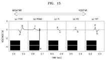
FIG. 15 illustrates charging characteristics of a MoS2 material. InFIG. 15 , a MoS2 material is used as the energy generation layer, and output voltages generated when the MoS2 material contacts other materials. In detail, inFIG. 15 , "(a) Poly Tetra Fluoro Ethylene (PTFE)", "(b) Poly DiMethyl Siloxane (PDMS)", "(c) Poly Imide (PI)", "(d) Poly Carbonate (PC)", and "(e) Poly Ethylene Terephthalate (PET)" illustrate output voltages generated when the MoS2 material contacts PTFE, PDMS, PI, PC, and PET, respectively. InFIG. 15 , "P" denotes a case in which the MoS2 material is pressed to be close to other material, and "R" denotes a case in which the pressed MoS2 material is released to be separated from other material. Referring toFIG. 15 , it may be seen that the MoS2 material has friction electricity characteristics and the charging characteristics of the MoS2 material is between the charging characteristics of PDMS and the charging characteristics of PTFE. -
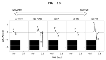
FIG. 16 illustrates charging characteristics of a WS2 material. InFIG. 16 , a MoS2 material is used as the energy generation layer, and output voltages generated when the WS2 material contacts other material are illustrated. In detail, inFIG. 16 , "(a) PTFE", "(b) PDMS", "(c) PI", "(d) PC", and "(e) PET" illustrate output voltages generated when the WS2 material contacts PTFE, PDMS, PI, PC, and PET. InFIG. 16 , "P" denotes a case in which the WS2 material is pressed to be close to other material, and "R" denotes a case in which the pressed WS2 material is released to be separated from other material. Referring toFIG. 16 , it may be seen that the WS2 material has friction electricity characteristics and the charging characteristics of the WS2 material is located at a position that is more negative than the charging characteristics of PTFE. -
FIGS. 17A and 17B illustrate a method of manufacturing a triboelectric generator including graphene having a shape of a wavy pattern by using stretchability of a PDMS substrate, according to at least one example embodiment. - First, referring to
FIG. 17A , after a PDMS substrate is stretched, graphene is formed on an upper surface of the stretched PDMS substrate. A Poly Methyl Meth Acrylate (PMMA) substrate on which a Cu electrode is deposited is provided on an upper portion of the PDMS substrate. Next, referring toFIG. 17B , when the stretched PDMS substrate is contracted to an original state, the upper surface of the PDMS substrate may have the shape of a wavy pattern due to contraction. Accordingly, the graphene formed on the upper surface of the PDMS substrate may have the shape of a wavy pattern. -
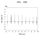
FIGS. 18A to 18C illustrate output voltages generated as graphene and a PMMA substrate are contacted with each other, in the triboelectric generator manufactured according to the elongation percentage of PDMS inFIGS. 17A and 17B . In detail,FIG. 18A illustrates a case in which an elongation percentage of the PDMS substrate is 0%, in other words, the PDMS substrate is not stretched, so that graphene is not formed in a wavy pattern.FIG. 18B illustrates a case in which the PDMS substrate is stretched by 10% and then restored so that graphene having the shape of a wavy pattern is formed.FIG. 18C illustrates a case in which the PDMS substrate is stretched by 20% and then restored, so that graphene having the shape of a wavy pattern is formed. - When the graphene has the shape of a wavy pattern, as illustrated in
FIGS. 18B and18C , friction electricity generated per unit area is increased, compared to the graphene ofFIG. 18A . - As described above, the triboelectric generators according to the example embodiments include the energy generation layer that may generate electric energy through friction with other material having different charging characteristics, and the energy generation layer may include at a 1 D nanomaterial and/or a 2D material. Also, when a flexible and stretchable substrate is used as the substrate, the electrode provided on the substrate, and the energy generation layer, may have flexibility and stretchability corresponding to, similar to or the same as the flexibility and stretchability of the substrate. Accordingly, the triboelectric generator manufactured by using the substrate having flexibility and stretchability may effectively generate electric energy due to external environment factors such as wind, sound, or movements of a person. Also, the amount of electric energy output may be increased by, for example, vertically stacking a plurality of triboelectric generators and serially connecting the triboelectric generators. The triboelectric generator may generate electric energy that can be used in, for example, portable electronic devices, clothes, bags, hats, gloves, or flags or by being attached on a body part of a person.
- It should be understood that example embodiments described herein should be considered in a descriptive sense only and not for purposes of limitation. Descriptions of features within each example embodiment should typically be considered as available for other similar or same features in other example embodiments.
Claims (15)
- A triboelectric generator comprising:first and second electrodes facing each other; anda first energy generation layer on the first electrode and configured to generate electric energy by contact with at least one other material, the first energy generation layer comprising a two-dimensional (2D) material having a crystal structure of a 2D shape.
- The triboelectric generator of claim 1, wherein the two-dimensional material comprises at least one of hexagonal-boron nitride (h-BN) and transition metal dichalcogenide (TMD) and optionally wherein the 2D material has a single layer or a multilayer structure.
- The triboelectric generator of claim 2, wherein the TMD comprises one of Mo, W, Nb, V, Ta, Ti, Zr, Hf, Tc, Re, Cu, Ga, In, Sn, Ge, and Pb, and one of S, Se, and Te.
- The triboelectric generator of any preceding claim, wherein the 2D material has a thickness of 0.3 nm to 1000 nm.
- The triboelectric generator of any preceding claim, further comprising a spacer between the first electrode and the second electrode.
- The triboelectric generator of any preceding claim, wherein the first energy layer generates electric energy by contact with the second electrode.
- The triboelectric generator of any preceding claim, further comprising at least one of a first substrate on which the first electrode and the first energy generation layer are located and a second substrate on which the second electrode is located,
and optionally wherein the first energy generation layer is configured to generate electric energy by contact with the second electrode or the second substrate. - The triboelectric generator of claim 7, wherein at least one of the first and second substrates is stretchable, and
optionally wherein the at least one of the first and second substrates has an elongation percentage of about 200% or lower.. - The triboelectric generator of claim 7 or 8, wherein the at least one of the first and second substrates comprises at least one of polydimethylsiloxane (PDMS), polyimide (PI), Teflon, urethane, and nylon.
- The triboelectric generator of claim 7, 8 or 9, wherein the at least one of the first and second substrates has a surface having a wavy shape,
and optionally wherein the first electrode and the first energy generation layer have a shape corresponding to a surface of the first substrate, and the second electrode has a shape corresponding to a surface of the second substrate. - The triboelectric generator of claim 7, 8, 9 or 10, wherein at least one of the first and second electrodes comprises at least one of carbon nanotube (CNT), graphene, Ag nanowire, metal, and metal mesh.
- The triboelectric generator of any preceding claim, further comprising a second energy generation layer on the second electrode and configured to generate electric energy by contact with the first energy generation layer,
and optionally further comprising at least one of a first substrate on which the first electrode and the first energy generation layer are located and a second substrate on which the second electrode and the second energy generation layer are located. - A triboelectric generator comprising:first and second electrodes facing each other and having stretchability; anda first energy generation layer on the first electrode and configured to generate electric energy by contact with at least one other material,and optionally wherein the first energy generation layer comprises at least one of a one-dimensional (1D) material having a 1D shape of a nano size and a two-dimensional (2D) material having a crystal structure of a 2D shape.
- A triboelectric generator comprising:a plurality of energy generation units that are stacked,wherein at least one of the energy generation units is a triboelectric generator according to any preceding claim.
- The triboelectric generator of claim 14, wherein the energy generation units are serially connected to one another.
Applications Claiming Priority (2)
| Application Number | Priority Date | Filing Date | Title |
|---|---|---|---|
| KR20150056003 | 2015-04-21 | ||
| KR1020150138615A KR102553838B1 (en) | 2015-04-21 | 2015-10-01 | Triboelectric generator |
Publications (3)
| Publication Number | Publication Date |
|---|---|
| EP3086460A2 true EP3086460A2 (en) | 2016-10-26 |
| EP3086460A3 EP3086460A3 (en) | 2017-03-29 |
| EP3086460B1 EP3086460B1 (en) | 2022-12-21 |
Family
ID=55701765
Family Applications (1)
| Application Number | Title | Priority Date | Filing Date |
|---|---|---|---|
| EP16163889.5A Active EP3086460B1 (en) | 2015-04-21 | 2016-04-05 | Triboelectric generator |
Country Status (3)
| Country | Link |
|---|---|
| US (1) | US10199958B2 (en) |
| EP (1) | EP3086460B1 (en) |
| CN (1) | CN106067739B (en) |
Cited By (3)
| Publication number | Priority date | Publication date | Assignee | Title |
|---|---|---|---|---|
| CN108233762A (en) * | 2018-03-22 | 2018-06-29 | 大连理工大学 | A kind of flexible wearable friction nanometer power generator of comprehensive multi-mode collecting mechanical energy |
| WO2019073317A1 (en) * | 2017-10-11 | 2019-04-18 | Sabic Global Technologies B.V. | Polymer-graphene oxide triboelectric materials, methods of making and uses thereof |
| CN113783471A (en) * | 2021-07-16 | 2021-12-10 | 浙江大学 | Thin film dynamic semiconductor-polymer semiconductor heterojunction direct current generator and preparation method thereof |
Families Citing this family (23)
| Publication number | Priority date | Publication date | Assignee | Title |
|---|---|---|---|---|
| EP3120450B1 (en) * | 2014-03-18 | 2019-11-20 | Fondazione Istituto Italiano di Tecnologia | Triboelectric composite for mechanical energy harvesting and sensing |
| KR101544326B1 (en) * | 2014-10-15 | 2015-08-12 | 성균관대학교산학협력단 | Electrostatic energy harvester coupled with improved transparency and mechanical property using two dimensioinal material on ferroelectric or piezoelectric material |
| KR101557245B1 (en) * | 2014-12-03 | 2015-10-21 | 성균관대학교산학협력단 | Triboelectric energy generator using tire cord fabric |
| US10199958B2 (en) * | 2015-04-21 | 2019-02-05 | Samsung Electronics Co., Ltd. | Triboelectric generator |
| CN104811089A (en) * | 2015-05-19 | 2015-07-29 | 京东方科技集团股份有限公司 | Triboelectrification device and manufacturing method thereof, as well as electronic equipment and wearable equipment |
| CN105207517B (en) * | 2015-08-26 | 2017-08-25 | 京东方科技集团股份有限公司 | Triboelectricity device and its manufacture method |
| JP6645161B2 (en) * | 2015-12-11 | 2020-02-14 | 株式会社リコー | Power generator |
| US10900930B2 (en) * | 2016-07-15 | 2021-01-26 | United States Of America As Represented By The Administrator Of Nasa | Method for phonon assisted creation and annihilation of subsurface electric dipoles |
| CN106602924A (en) * | 2016-11-18 | 2017-04-26 | 北京纳米能源与系统研究所 | Frictional nano-generator for collecting vibration energy and vibration sensor |
| US20210135600A1 (en) * | 2016-12-22 | 2021-05-06 | Board Of Trustees Of The University Of Arkansas | Energy harvesting devices and sensors, and methods of making and use thereof |
| CN109149992B (en) * | 2017-06-15 | 2020-03-10 | 北京纳米能源与系统研究所 | Improved friction nano generator |
| US10804818B2 (en) * | 2017-06-30 | 2020-10-13 | Toyota Motor Engineering & Manufacturing North America, Inc. | Triboelectric generator and network for mechanical energy harvesting |
| KR102213229B1 (en) * | 2017-11-22 | 2021-02-04 | 송찰스기석 | Triboelectric power generating device and method for preparing the same |
| US10774618B2 (en) * | 2018-03-16 | 2020-09-15 | Baker Hughes, A Ge Company, Llc | Autonomous downhole power generator module |
| DE102018221047A1 (en) * | 2018-04-05 | 2019-10-10 | Continental Reifen Deutschland Gmbh | Apparatus for measuring a mechanical force comprising first, second, third, fourth and fifth layers and the uses of the apparatus and tires or engineering rubber articles comprising the apparatus |
| CA3101791A1 (en) * | 2018-05-30 | 2019-12-05 | Board Of Trustees Of The University Of Arkansas | Energy harvesting devices and sensors, and methods of making and use thereof |
| US11276644B2 (en) * | 2018-12-17 | 2022-03-15 | Intel Corporation | Integrated circuits and methods for forming thin film crystal layers |
| CN109889081B (en) * | 2019-04-10 | 2020-09-04 | 苏州大学 | Single-electrode mode stretchable friction nano generator and preparation method thereof |
| KR20210077157A (en) * | 2019-12-17 | 2021-06-25 | 송찰스기석 | Triboelectric power generating device with separation membrane and method for preparing the same |
| CN111245081B (en) * | 2020-01-21 | 2023-06-20 | 电子科技大学 | Self-powered automobile exhaust sensor and method |
| US11478191B1 (en) * | 2020-04-03 | 2022-10-25 | Esatto Healthcare, Inc. | Smart mask for COVID-19 screening, tracking and monitoring |
| CN116547897A (en) | 2020-04-22 | 2023-08-04 | 阿肯色大学技术创业公司 | Device for collecting environmental heat energy and vibration energy |
| CN114106639A (en) * | 2021-11-19 | 2022-03-01 | 兰州理工大学 | High-friction charge density and wear-resistant triboelectric material and application thereof |
Family Cites Families (24)
| Publication number | Priority date | Publication date | Assignee | Title |
|---|---|---|---|---|
| KR101435999B1 (en) | 2007-12-07 | 2014-08-29 | 삼성전자주식회사 | Reduced graphene oxide doped by dopant, thin layer and transparent electrode |
| KR101450591B1 (en) | 2008-06-05 | 2014-10-17 | 삼성전자주식회사 | CNT n-doping materials and method, device using the same |
| KR101634753B1 (en) | 2008-11-28 | 2016-06-30 | 삼성전자주식회사 | CNT n-doping materials and CNT n-doping method employing the same |
| US8803406B2 (en) | 2010-11-30 | 2014-08-12 | KAIST (Korea Advanced Institute of Science and Technology) | Flexible nanocomposite generator and method for manufacturing the same |
| US9178446B2 (en) | 2011-08-30 | 2015-11-03 | Georgia Tech Research Corporation | Triboelectric generator |
| KR101471845B1 (en) | 2012-06-29 | 2014-12-11 | 엘지디스플레이 주식회사 | Display device with input system and method for driving the same |
| US9812993B2 (en) | 2012-09-21 | 2017-11-07 | Georgia Tech Research Corporation | Single electrode triboelectric generator |
| US9790928B2 (en) * | 2012-09-21 | 2017-10-17 | Georgia Tech Research Corporation | Triboelectric generators and sensors |
| US9985554B2 (en) | 2013-03-01 | 2018-05-29 | Georgia Tech Research Corporation | Triboelectric nanogenerator |
| KR101992495B1 (en) | 2013-02-07 | 2019-06-25 | 도레이첨단소재 주식회사 | Side sealant for flexible substrate element |
| US9571009B2 (en) | 2013-03-01 | 2017-02-14 | Georgia Tech Research Corporation | Rotating cylindrical and spherical triboelectric generators |
| US9484842B2 (en) | 2013-03-01 | 2016-11-01 | Georgia Tech Research Corporation | Segmentally structured disk triboelectric nanogenerator |
| KR20140126607A (en) | 2013-04-23 | 2014-10-31 | 삼성전자주식회사 | Smart apparatus having touch input module and energy generating device, and operating method of the smart apparatus |
| KR101498595B1 (en) | 2013-05-31 | 2015-03-04 | 전자부품연구원 | Triboelectric Generator |
| CN104242723B (en) | 2013-06-13 | 2019-06-04 | 北京纳米能源与系统研究所 | Single electrode friction nanometer power generator, electricity-generating method and from driving follow-up mechanism |
| CN104300828B (en) | 2013-07-19 | 2017-06-16 | 纳米新能源(唐山)有限责任公司 | A kind of friction generator |
| KR102103987B1 (en) | 2013-09-02 | 2020-04-24 | 삼성전자주식회사 | Textile-based energy generator |
| US10199958B2 (en) * | 2015-04-21 | 2019-02-05 | Samsung Electronics Co., Ltd. | Triboelectric generator |
| US10305020B2 (en) * | 2015-05-15 | 2019-05-28 | Ricoh Company, Ltd. | Element and electric generator |
| KR102455431B1 (en) * | 2015-06-02 | 2022-10-17 | 삼성전자주식회사 | Triboelectric generator |
| JP6645161B2 (en) * | 2015-12-11 | 2020-02-14 | 株式会社リコー | Power generator |
| US10770990B2 (en) * | 2016-05-10 | 2020-09-08 | Samsung Electronics Co., Ltd. | Triboelectric generator |
| KR102578823B1 (en) * | 2016-05-10 | 2023-09-15 | 삼성전자주식회사 | Triboelectric generator |
| KR102600148B1 (en) * | 2016-08-23 | 2023-11-08 | 삼성전자주식회사 | Triboelectric generator using surface plasmon resonance |
-
2016
- 2016-02-22 US US15/049,726 patent/US10199958B2/en active Active
- 2016-04-05 EP EP16163889.5A patent/EP3086460B1/en active Active
- 2016-04-19 CN CN201610244475.4A patent/CN106067739B/en active Active
Non-Patent Citations (1)
| Title |
|---|
| None |
Cited By (5)
| Publication number | Priority date | Publication date | Assignee | Title |
|---|---|---|---|---|
| WO2019073317A1 (en) * | 2017-10-11 | 2019-04-18 | Sabic Global Technologies B.V. | Polymer-graphene oxide triboelectric materials, methods of making and uses thereof |
| CN108233762A (en) * | 2018-03-22 | 2018-06-29 | 大连理工大学 | A kind of flexible wearable friction nanometer power generator of comprehensive multi-mode collecting mechanical energy |
| CN108233762B (en) * | 2018-03-22 | 2023-12-22 | 大连理工大学 | Flexible wearable friction nano generator capable of collecting mechanical energy in omnibearing multimode mode |
| CN113783471A (en) * | 2021-07-16 | 2021-12-10 | 浙江大学 | Thin film dynamic semiconductor-polymer semiconductor heterojunction direct current generator and preparation method thereof |
| CN113783471B (en) * | 2021-07-16 | 2023-12-08 | 浙江大学 | Thin film dynamic semiconductor-polymer semiconductor heterojunction direct current generator and preparation method thereof |
Also Published As
| Publication number | Publication date |
|---|---|
| CN106067739B (en) | 2020-01-17 |
| EP3086460A3 (en) | 2017-03-29 |
| US10199958B2 (en) | 2019-02-05 |
| CN106067739A (en) | 2016-11-02 |
| EP3086460B1 (en) | 2022-12-21 |
| US20160315561A1 (en) | 2016-10-27 |
Similar Documents
| Publication | Publication Date | Title |
|---|---|---|
| US10199958B2 (en) | Triboelectric generator | |
| KR102553838B1 (en) | Triboelectric generator | |
| Hu et al. | Strategies to achieve high performance piezoelectric nanogenerators | |
| Lee et al. | Piezoelectric energy harvesting from two-dimensional boron nitride nanoflakes | |
| Zong et al. | Graphene-based thermoelectrics | |
| Liu et al. | Improvement in the piezoelectric performance of a ZnO nanogenerator by a combination of chemical doping and interfacial modification | |
| Lee et al. | All-in-one energy harvesting and storage devices | |
| Hu et al. | Recent advancements in nanogenerators for energy harvesting | |
| Wang et al. | Piezoelectric nanogenerators based on zinc oxide nanowire arrays | |
| Zhou et al. | Biomimetic approach to facilitate the high filler content in free-standing and flexible thermoelectric polymer composite films based on PVDF and Ag2Se nanowires | |
| Choi et al. | Highly surface-embossed polydimethylsiloxane-based triboelectric nanogenerators with hierarchically nanostructured conductive Ni–Cu fabrics | |
| Van Ngoc et al. | Flexible, transparent and exceptionally high power output nanogenerators based on ultrathin ZnO nanoflakes | |
| Yoon et al. | Synergistic contribution of flexoelectricity and piezoelectricity towards a stretchable robust nanogenerator for wearable electronics | |
| US9160197B2 (en) | Apparatus for generating and storing electric energy | |
| Shin et al. | Solvent-assisted optimal BaTiO3 nanoparticles-polymer composite cluster formation for high performance piezoelectric nanogenerators | |
| KR20130137253A (en) | Flexible multi-layered thermoelectric device with enhanced thermoelectric ability and preparation thereof | |
| Zhang et al. | Nanogenerator made of ZnO nanosheet networks | |
| Lee et al. | Nanostructured inorganic chalcogenide-carbon nanotube yarn having a high thermoelectric power factor at low temperature | |
| Nguyen et al. | based ZnO nanogenerator using contact electrification and piezoelectric effects | |
| Baek et al. | Flexible piezoelectric nanogenerators based on a transferred ZnO nanorod/Si micro-pillar array | |
| Wang et al. | Tailoring highly flexible hybrid supercapacitors developed by graphite nanoplatelets-based film: toward integrated wearable energy platform building blocks | |
| Fuh et al. | All-fiber transparent piezoelectric harvester with a cooperatively enhanced structure | |
| Kim et al. | Triboelectric charge-driven enhancement of the output voltage of BiSbTe-based thermoelectric generators | |
| Han et al. | Stretchable inorganic GaN-nanowire photosensor with high photocurrent and photoresponsivity | |
| Mondal et al. | Self-charging piezo-supercapacitor: one-step mechanical energy conversion and storage |
Legal Events
| Date | Code | Title | Description |
|---|---|---|---|
| PUAI | Public reference made under article 153(3) epc to a published international application that has entered the european phase |
Free format text: ORIGINAL CODE: 0009012 |
|
| AK | Designated contracting states |
Kind code of ref document: A2 Designated state(s): AL AT BE BG CH CY CZ DE DK EE ES FI FR GB GR HR HU IE IS IT LI LT LU LV MC MK MT NL NO PL PT RO RS SE SI SK SM TR |
|
| AX | Request for extension of the european patent |
Extension state: BA ME |
|
| RIC1 | Information provided on ipc code assigned before grant |
Ipc: H02N 1/04 20060101AFI20161021BHEP |
|
| PUAL | Search report despatched |
Free format text: ORIGINAL CODE: 0009013 |
|
| AK | Designated contracting states |
Kind code of ref document: A3 Designated state(s): AL AT BE BG CH CY CZ DE DK EE ES FI FR GB GR HR HU IE IS IT LI LT LU LV MC MK MT NL NO PL PT RO RS SE SI SK SM TR |
|
| AX | Request for extension of the european patent |
Extension state: BA ME |
|
| RIC1 | Information provided on ipc code assigned before grant |
Ipc: H02N 1/04 20060101AFI20170220BHEP |
|
| STAA | Information on the status of an ep patent application or granted ep patent |
Free format text: STATUS: REQUEST FOR EXAMINATION WAS MADE |
|
| 17P | Request for examination filed |
Effective date: 20170814 |
|
| RBV | Designated contracting states (corrected) |
Designated state(s): AL AT BE BG CH CY CZ DE DK EE ES FI FR GB GR HR HU IE IS IT LI LT LU LV MC MK MT NL NO PL PT RO RS SE SI SK SM TR |
|
| STAA | Information on the status of an ep patent application or granted ep patent |
Free format text: STATUS: EXAMINATION IS IN PROGRESS |
|
| 17Q | First examination report despatched |
Effective date: 20200416 |
|
| STAA | Information on the status of an ep patent application or granted ep patent |
Free format text: STATUS: EXAMINATION IS IN PROGRESS |
|
| GRAP | Despatch of communication of intention to grant a patent |
Free format text: ORIGINAL CODE: EPIDOSNIGR1 |
|
| STAA | Information on the status of an ep patent application or granted ep patent |
Free format text: STATUS: GRANT OF PATENT IS INTENDED |
|
| INTG | Intention to grant announced |
Effective date: 20220113 |
|
| GRAJ | Information related to disapproval of communication of intention to grant by the applicant or resumption of examination proceedings by the epo deleted |
Free format text: ORIGINAL CODE: EPIDOSDIGR1 |
|
| STAA | Information on the status of an ep patent application or granted ep patent |
Free format text: STATUS: EXAMINATION IS IN PROGRESS |
|
| INTC | Intention to grant announced (deleted) | ||
| GRAP | Despatch of communication of intention to grant a patent |
Free format text: ORIGINAL CODE: EPIDOSNIGR1 |
|
| STAA | Information on the status of an ep patent application or granted ep patent |
Free format text: STATUS: GRANT OF PATENT IS INTENDED |
|
| INTG | Intention to grant announced |
Effective date: 20220711 |
|
| GRAS | Grant fee paid |
Free format text: ORIGINAL CODE: EPIDOSNIGR3 |
|
| GRAA | (expected) grant |
Free format text: ORIGINAL CODE: 0009210 |
|
| STAA | Information on the status of an ep patent application or granted ep patent |
Free format text: STATUS: THE PATENT HAS BEEN GRANTED |
|
| AK | Designated contracting states |
Kind code of ref document: B1 Designated state(s): AL AT BE BG CH CY CZ DE DK EE ES FI FR GB GR HR HU IE IS IT LI LT LU LV MC MK MT NL NO PL PT RO RS SE SI SK SM TR |
|
| REG | Reference to a national code |
Ref country code: GB Ref legal event code: FG4D |
|
| REG | Reference to a national code |
Ref country code: CH Ref legal event code: EP |
|
| REG | Reference to a national code |
Ref country code: DE Ref legal event code: R096 Ref document number: 602016076975 Country of ref document: DE |
|
| REG | Reference to a national code |
Ref country code: AT Ref legal event code: REF Ref document number: 1539640 Country of ref document: AT Kind code of ref document: T Effective date: 20230115 |
|
| REG | Reference to a national code |
Ref country code: IE Ref legal event code: FG4D |
|
| REG | Reference to a national code |
Ref country code: LT Ref legal event code: MG9D |
|
| REG | Reference to a national code |
Ref country code: NL Ref legal event code: MP Effective date: 20221221 |
|
| PG25 | Lapsed in a contracting state [announced via postgrant information from national office to epo] |
Ref country code: SE Free format text: LAPSE BECAUSE OF FAILURE TO SUBMIT A TRANSLATION OF THE DESCRIPTION OR TO PAY THE FEE WITHIN THE PRESCRIBED TIME-LIMIT Effective date: 20221221 Ref country code: NO Free format text: LAPSE BECAUSE OF FAILURE TO SUBMIT A TRANSLATION OF THE DESCRIPTION OR TO PAY THE FEE WITHIN THE PRESCRIBED TIME-LIMIT Effective date: 20230321 Ref country code: LT Free format text: LAPSE BECAUSE OF FAILURE TO SUBMIT A TRANSLATION OF THE DESCRIPTION OR TO PAY THE FEE WITHIN THE PRESCRIBED TIME-LIMIT Effective date: 20221221 Ref country code: FI Free format text: LAPSE BECAUSE OF FAILURE TO SUBMIT A TRANSLATION OF THE DESCRIPTION OR TO PAY THE FEE WITHIN THE PRESCRIBED TIME-LIMIT Effective date: 20221221 |
|
| PGFP | Annual fee paid to national office [announced via postgrant information from national office to epo] |
Ref country code: FR Payment date: 20230328 Year of fee payment: 8 |
|
| REG | Reference to a national code |
Ref country code: AT Ref legal event code: MK05 Ref document number: 1539640 Country of ref document: AT Kind code of ref document: T Effective date: 20221221 |
|
| PG25 | Lapsed in a contracting state [announced via postgrant information from national office to epo] |
Ref country code: RS Free format text: LAPSE BECAUSE OF FAILURE TO SUBMIT A TRANSLATION OF THE DESCRIPTION OR TO PAY THE FEE WITHIN THE PRESCRIBED TIME-LIMIT Effective date: 20221221 Ref country code: LV Free format text: LAPSE BECAUSE OF FAILURE TO SUBMIT A TRANSLATION OF THE DESCRIPTION OR TO PAY THE FEE WITHIN THE PRESCRIBED TIME-LIMIT Effective date: 20221221 Ref country code: HR Free format text: LAPSE BECAUSE OF FAILURE TO SUBMIT A TRANSLATION OF THE DESCRIPTION OR TO PAY THE FEE WITHIN THE PRESCRIBED TIME-LIMIT Effective date: 20221221 Ref country code: GR Free format text: LAPSE BECAUSE OF FAILURE TO SUBMIT A TRANSLATION OF THE DESCRIPTION OR TO PAY THE FEE WITHIN THE PRESCRIBED TIME-LIMIT Effective date: 20230322 |
|
| PGFP | Annual fee paid to national office [announced via postgrant information from national office to epo] |
Ref country code: GB Payment date: 20230323 Year of fee payment: 8 |
|
| P01 | Opt-out of the competence of the unified patent court (upc) registered |
Effective date: 20230520 |
|
| PG25 | Lapsed in a contracting state [announced via postgrant information from national office to epo] |
Ref country code: NL Free format text: LAPSE BECAUSE OF FAILURE TO SUBMIT A TRANSLATION OF THE DESCRIPTION OR TO PAY THE FEE WITHIN THE PRESCRIBED TIME-LIMIT Effective date: 20221221 |
|
| PG25 | Lapsed in a contracting state [announced via postgrant information from national office to epo] |
Ref country code: SM Free format text: LAPSE BECAUSE OF FAILURE TO SUBMIT A TRANSLATION OF THE DESCRIPTION OR TO PAY THE FEE WITHIN THE PRESCRIBED TIME-LIMIT Effective date: 20221221 Ref country code: RO Free format text: LAPSE BECAUSE OF FAILURE TO SUBMIT A TRANSLATION OF THE DESCRIPTION OR TO PAY THE FEE WITHIN THE PRESCRIBED TIME-LIMIT Effective date: 20221221 Ref country code: PT Free format text: LAPSE BECAUSE OF FAILURE TO SUBMIT A TRANSLATION OF THE DESCRIPTION OR TO PAY THE FEE WITHIN THE PRESCRIBED TIME-LIMIT Effective date: 20230421 Ref country code: ES Free format text: LAPSE BECAUSE OF FAILURE TO SUBMIT A TRANSLATION OF THE DESCRIPTION OR TO PAY THE FEE WITHIN THE PRESCRIBED TIME-LIMIT Effective date: 20221221 Ref country code: EE Free format text: LAPSE BECAUSE OF FAILURE TO SUBMIT A TRANSLATION OF THE DESCRIPTION OR TO PAY THE FEE WITHIN THE PRESCRIBED TIME-LIMIT Effective date: 20221221 Ref country code: CZ Free format text: LAPSE BECAUSE OF FAILURE TO SUBMIT A TRANSLATION OF THE DESCRIPTION OR TO PAY THE FEE WITHIN THE PRESCRIBED TIME-LIMIT Effective date: 20221221 Ref country code: AT Free format text: LAPSE BECAUSE OF FAILURE TO SUBMIT A TRANSLATION OF THE DESCRIPTION OR TO PAY THE FEE WITHIN THE PRESCRIBED TIME-LIMIT Effective date: 20221221 |
|
| PGFP | Annual fee paid to national office [announced via postgrant information from national office to epo] |
Ref country code: DE Payment date: 20230321 Year of fee payment: 8 |
|
| PG25 | Lapsed in a contracting state [announced via postgrant information from national office to epo] |
Ref country code: SK Free format text: LAPSE BECAUSE OF FAILURE TO SUBMIT A TRANSLATION OF THE DESCRIPTION OR TO PAY THE FEE WITHIN THE PRESCRIBED TIME-LIMIT Effective date: 20221221 Ref country code: PL Free format text: LAPSE BECAUSE OF FAILURE TO SUBMIT A TRANSLATION OF THE DESCRIPTION OR TO PAY THE FEE WITHIN THE PRESCRIBED TIME-LIMIT Effective date: 20221221 Ref country code: IS Free format text: LAPSE BECAUSE OF FAILURE TO SUBMIT A TRANSLATION OF THE DESCRIPTION OR TO PAY THE FEE WITHIN THE PRESCRIBED TIME-LIMIT Effective date: 20230421 Ref country code: AL Free format text: LAPSE BECAUSE OF FAILURE TO SUBMIT A TRANSLATION OF THE DESCRIPTION OR TO PAY THE FEE WITHIN THE PRESCRIBED TIME-LIMIT Effective date: 20221221 |
|
| REG | Reference to a national code |
Ref country code: DE Ref legal event code: R097 Ref document number: 602016076975 Country of ref document: DE |
|
| PLBE | No opposition filed within time limit |
Free format text: ORIGINAL CODE: 0009261 |
|
| STAA | Information on the status of an ep patent application or granted ep patent |
Free format text: STATUS: NO OPPOSITION FILED WITHIN TIME LIMIT |
|
| PG25 | Lapsed in a contracting state [announced via postgrant information from national office to epo] |
Ref country code: DK Free format text: LAPSE BECAUSE OF FAILURE TO SUBMIT A TRANSLATION OF THE DESCRIPTION OR TO PAY THE FEE WITHIN THE PRESCRIBED TIME-LIMIT Effective date: 20221221 |
|
| 26N | No opposition filed |
Effective date: 20230922 |
|
| REG | Reference to a national code |
Ref country code: CH Ref legal event code: PL |
|
| PG25 | Lapsed in a contracting state [announced via postgrant information from national office to epo] |
Ref country code: LU Free format text: LAPSE BECAUSE OF NON-PAYMENT OF DUE FEES Effective date: 20230405 |
|
| REG | Reference to a national code |
Ref country code: BE Ref legal event code: MM Effective date: 20230430 |
|
| PG25 | Lapsed in a contracting state [announced via postgrant information from national office to epo] |
Ref country code: MC Free format text: LAPSE BECAUSE OF FAILURE TO SUBMIT A TRANSLATION OF THE DESCRIPTION OR TO PAY THE FEE WITHIN THE PRESCRIBED TIME-LIMIT Effective date: 20221221 |
|
| PG25 | Lapsed in a contracting state [announced via postgrant information from national office to epo] |
Ref country code: SI Free format text: LAPSE BECAUSE OF FAILURE TO SUBMIT A TRANSLATION OF THE DESCRIPTION OR TO PAY THE FEE WITHIN THE PRESCRIBED TIME-LIMIT Effective date: 20221221 Ref country code: MC Free format text: LAPSE BECAUSE OF FAILURE TO SUBMIT A TRANSLATION OF THE DESCRIPTION OR TO PAY THE FEE WITHIN THE PRESCRIBED TIME-LIMIT Effective date: 20221221 Ref country code: LI Free format text: LAPSE BECAUSE OF NON-PAYMENT OF DUE FEES Effective date: 20230430 Ref country code: CH Free format text: LAPSE BECAUSE OF NON-PAYMENT OF DUE FEES Effective date: 20230430 |
|
| REG | Reference to a national code |
Ref country code: IE Ref legal event code: MM4A |
|
| PG25 | Lapsed in a contracting state [announced via postgrant information from national office to epo] |
Ref country code: BE Free format text: LAPSE BECAUSE OF NON-PAYMENT OF DUE FEES Effective date: 20230430 |
|
| PG25 | Lapsed in a contracting state [announced via postgrant information from national office to epo] |
Ref country code: IE Free format text: LAPSE BECAUSE OF NON-PAYMENT OF DUE FEES Effective date: 20230405 |