EP3085474B1 - Konstruktionsbauteil eines technischen gegenstands sowie verfahren zur herstellung des konstruktionsbauteils - Google Patents
Konstruktionsbauteil eines technischen gegenstands sowie verfahren zur herstellung des konstruktionsbauteils Download PDFInfo
- Publication number
- EP3085474B1 EP3085474B1 EP16164876.1A EP16164876A EP3085474B1 EP 3085474 B1 EP3085474 B1 EP 3085474B1 EP 16164876 A EP16164876 A EP 16164876A EP 3085474 B1 EP3085474 B1 EP 3085474B1
- Authority
- EP
- European Patent Office
- Prior art keywords
- electrical component
- casting
- layer
- component
- electrical
- Prior art date
- Legal status (The legal status is an assumption and is not a legal conclusion. Google has not performed a legal analysis and makes no representation as to the accuracy of the status listed.)
- Not-in-force
Links
Images

Classifications
-
- B—PERFORMING OPERATIONS; TRANSPORTING
- B22—CASTING; POWDER METALLURGY
- B22D—CASTING OF METALS; CASTING OF OTHER SUBSTANCES BY THE SAME PROCESSES OR DEVICES
- B22D19/00—Casting in, on, or around objects which form part of the product
- B22D19/04—Casting in, on, or around objects which form part of the product for joining parts
-
- B—PERFORMING OPERATIONS; TRANSPORTING
- B22—CASTING; POWDER METALLURGY
- B22D—CASTING OF METALS; CASTING OF OTHER SUBSTANCES BY THE SAME PROCESSES OR DEVICES
- B22D19/00—Casting in, on, or around objects which form part of the product
- B22D19/0081—Casting in, on, or around objects which form part of the product pretreatment of the insert, e.g. for enhancing the bonding between insert and surrounding cast metal
-
- H—ELECTRICITY
- H10—SEMICONDUCTOR DEVICES; ELECTRIC SOLID-STATE DEVICES NOT OTHERWISE PROVIDED FOR
- H10W—GENERIC PACKAGES, INTERCONNECTIONS, CONNECTORS OR OTHER CONSTRUCTIONAL DETAILS OF DEVICES COVERED BY CLASS H10
- H10W74/00—Encapsulations, e.g. protective coatings
- H10W74/10—Encapsulations, e.g. protective coatings characterised by their shape or disposition
- H10W74/111—Encapsulations, e.g. protective coatings characterised by their shape or disposition the semiconductor body being completely enclosed
Definitions
- the invention relates to a structural component of a technical object according to claim 1.
- the invention also relates to a method for producing a structural component of the aforementioned type.
- the invention relates to the field of integration of electrical components in metal casting materials.
- electrical components may be electrical components of all types, from a simple electrical wire (cable) to electrical functional components, e.g. Sensors and / or actuators.
- From the JP 2005/109306 A is an epoxy resin molded electronic assembly out. From the DE 10 2010 046 170 A1 goes out a casting with cast transponder. From the DE 103 15 425 A1 is a method for producing a device with a piezoelectric component and a manufactured in this way device and sensor or actuator with such a device forth.
- the invention has for its object to provide components and methods that allow integration of an electrical component in a metal casting material by means of any casting process.
- the protective layer may consist of a protective material whose melting point is at the same or a higher temperature than the specified for the electrical component maximum Verg screentemperatur.
- the invention has the advantage that the electrical component is cast by means of an arbitrary casting process in a metallic casting material can. In particular, there is no restriction on diecasting. Any casting method that appears adequate for the application can be used, such as lost mold casting or permanent casting.
- the electrical component according to the invention retains its electrical functionality during and after the casting process and can then be used without restrictions.
- Thermal shock is the rapid, shock-like change in the temperature of the material or workpiece. This results in mechanical stresses between the outer and inner parts of the material, since the heat is transferred to or from the surface faster than to the interior.
- a component is considered pourable if it can be integrated in the casting material while maintaining the functionality of the component by means of a casting process.
- the invention is suitable for electrical components of any kind.
- an electrical component is thereby the smallest basic, considered as a single component of an electrical circuit both as a mathematical-physical phenomenon and in the form of an idealized device, as a real (discrete) component or as an assembly Roger that.
- an electrical component can be provided that can be specified for a maximum potting temperature ⁇ 400 ° Celsius or ⁇ 500 ° Celsius.
- the electrical component can be a passive electrical component, for example an electrical line (single-core or multi-core), an electrical or electronic circuit, a sensor and / or an actuator.
- the electrical component can be designed, for example, as an AMR sensor (AMR-anisotropic magnetoresistive effect), as a Hall sensor or as a strain sensor, for example based on platinum.
- the electrical component if it is designed as an actuator, for example, have a coil.
- the electrical component may be formed with or without a substrate.
- the electrical component has a substrate
- further electrical components can be arranged on the substrate, such as one or more sensor layers and / or actuator layers, as well as other material layers such as the above-mentioned electrically insulating material layer and the protective layer.
- the electrical component may comprise, for example, a substrate to which an electrically conductive layer is applied, which may serve as a sensor layer, for example, when the electrical component is designed as a sensor.
- the electrical component has at least one electrical sensor, an electrical actuator and / or another passive or active electrical component or consists thereof.
- the electrical component may be completely or partially coated with the electrically insulating material layer.
- the protective layer may completely encase the electrical component or only cover portions thereof, e.g. cover the electrically insulating material layer in whole or in part, or other surface areas of the electrical component.
- the protective layer acts like a protective shield, which can be at least superficially melted on the outer, executed to the casting material side of this, but which prevents melting through to the electrical component. This effect is quite advantageous because in this way a cohesive connection between the electrical component and the casting material can be produced. In this way, it is possible to provide an electrical component which can be bonded to the metallic cast material in a materially bonded manner.
- the electrical component for a particular metal casting material is specified in which it means the casting process is pourable.
- the electrical component has a substrate made of the same material as the specified casting material. This allows for an advantageous integration of the electrical component in the specified casting material. In particular, the same mechanical and thermal properties (coefficient of expansion) can be realized in this way, so that the electrical component fits well into the casting material in every respect. It also prevents adverse effects on the mechanical stability of a structural component, which is made of the metallic casting material.
- the protective layer is coated with an antioxidant layer of an antioxidant material, by which the protective layer is protected against oxidation.
- the melting point of the antioxidant layer is at a lower temperature than the maximum potting temperature specified for the electrical component.
- the above-described features of the electrical component may already be present before the electrical component has been cast in the metallic cast material, i. the corresponding properties are not generated during the pouring process.
- the structural component may e.g. be a motor vehicle component or a component of another technical subject. This also makes it possible to realize the advantages explained above.
- the electrical component is coated on its protective layer with an anti-oxidation layer with an antioxidant material. This has the advantage that in oxidation-susceptible protective materials unwanted oxidation can be avoided.
- the electrical component is cast in a metal casting material specified for the electrical component, wherein a material-locking connection between the protective material of the protective layer of the electrical component and the casting material is formed.
- an existing on the protective layer antioxidant layer is removed or at least broken in the course of H reducgitreaes. This has the advantage that the cohesive connection between the protective material and the casting material is not or only slightly disturbed by the antioxidant.
- the coating of the electrical component or a substrate with the electrically conductive layer, the electrically insulating material layer, the protective layer and / or the antioxidant layer can be carried out by one or several known methods, e.g. wet-chemical, by spraying, e.g. thermal cold gas spraying, or in a vacuum process such as e.g. Sputtering or a PVD or CVD process as well as dip coatings or roll plating processes.
- spraying e.g. thermal cold gas spraying
- a vacuum process such as e.g. Sputtering or a PVD or CVD process as well as dip coatings or roll plating processes.
- the said coating steps for the individual layers can e.g. be carried out in the same coating plant. If a particular layer is to be patterned, e.g. the electrically conductive layer to form a sensor layer, this can be done in a separate plant.
- the electrical component it is possible, in particular, for the electrical component to be cast in the metallic casting material without additional aids, such as, for example, positioning aids for positioning the electrical component during the casting process. It is not necessary that the electrical component is connected to or held by such a positioning aid. Rather, the electrical component itself can be held from the outside, ie from a region that is not potted with the metallic casting material. A certain portion of the electrical component is then out of the metallic casting material after the casting process. At this protruding portion, for example, electrical contacts of the electrical component can be arranged.
- This has the advantage that the entire production process is simplified, since in particular the electrical component does not have to be pretreated before the casting process, ie, does not have to be connected to a positioning element.
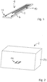
- the FIG. 1 shows a perspective view of an electrical component 1 in the form of an AMR sensor.
- the electrical component 1 has a sensor region 10 and an electrical contacting region 11.
- In the electrical contact area 11 are pads for connection, eg for soldering, electrical lines available to connect the sensor with an evaluation circuit.
- the electrical component 1 has a multilayer structure.
- On a substrate 3 different layers are applied, which will be described below with reference to the FIG. 3 be explained.
- a structured electrically conductive layer 4 which, in order to form an AMR sensor, is structured meander-shaped in the sensor region 10 and has the electrical connection surfaces in the contacting region 11.
- the electrical component 1 according to FIG. 1 is pourable in a metallic casting material.
- the FIG. 2 shows this by means of a construction component, the here by way of example is shown in fragmentary form and which is cast as a cast component 2 of a metallic casting material 20, wherein an electrical component 1 is cast into the casting material 20.
- the sensor region 10 is cast in the casting material 20.
- the contacting region 11 is apparent from it, so that it is accessible for connecting electrical lines.
- the FIG. 3 shows in detail the layer structure of the electrical component 1 based on a cross section through the component.
- the substrate 3 is coated on its surface side shown above with an electrically insulating material layer 4.
- On an electrically conductive material layer 5 is arranged.
- the electrically conductive material layer 5 is coated with a further electrically insulating material layer 6.
- On the electrically insulating material layer 6, a protective layer 7 is disposed of a protective material.
- an antioxidant layer 8 made of an antioxidant material is applied.
- the substrate 3 is initially coated, if necessary, with the protective layer 7.
- the antioxidant layer 8 is arranged.
- the electrical component 1 may be completely enveloped by the heat insulating layer 7 and the antioxidant layer 8, so that it is encapsulated by these layers. For electrical contacting of the electrical component 1 in the contacting region 11, it can be exposed at least at the connection surfaces of the layers 6, 7, 8.
- FIG. 4 shows a further embodiment of an electrical component 1 in the form of an electrical line, which may be formed, for example, as a rigid conductor or as a stranded wire. Visible is the concentric structure of several layers. Inside is an electrically conductive layer which forms an electrical conductor 9, for example in the form of a copper wire or a copper strand.
- the electrical conductor 9 is enveloped by an electrically insulating material layer 6, as explained above.
- the electrically insulating material layer 6 is enveloped by a protective layer 7.
- the protective layer 7 is of an antioxidant layer 8 wrapped.
- a single-core or multi-core electrical conduit may be provided as a pourable electrical component which may be cast in a metallic casting material.
- FIG. 5 shows a similar embodiment of an electrical component 1 as the FIG. 1 , In the form of an electrical line, in the case of FIG. 5 However, in the form of a coaxial cable with an inner conductor 9 and an outer conductor 12.
- the inner conductor 9 and / or the outer conductor 12 may be formed, for example, of copper or other suitable electrically conductive material.
- the inner conductor 9 is enveloped by an electrically insulating material layer 4.
- the electrically insulating material layer 4 is enveloped by the outer conductor 12.
- the outer conductor 12 is enveloped by a further electrically insulating material layer 6. This is in turn enveloped by the protective layer 7.
- the protective layer 7 is enveloped by the antioxidant layer 8.
- the layers 4, 5, 6, 7, 8 may be made relatively thin, e.g. in the range of 50 nm to 10 ⁇ m.
- the electrically conductive layer 5 may in particular have a layer thickness in the range of 100 nm to 300 nm.
- the insulating layers 4, 6 may in particular have a thickness in the range from 0.5 ⁇ m to 6 ⁇ m.
- the same material as the casting material 20 can be used as the material for the substrate 3.
- Suitable materials for the substrate are, for example, aluminum or steel.
- the electrical insulation layer 4, 6 may be formed, for example, as a sandwich layer by an inner layer is formed between two outer layers.
- a suitable material for the outer layers is, for example, alumina (Al 2 O 3 ) or hafnium carbide (HfC).
- a suitable material for the inner layer is, for example, silicon dioxide (SiO 2 ) or silicon carbide (SiC). Particularly advantageous is the use of a material for the insulating layer 4, which has an affinity or adhesive strength to the substrate material in terms of materials.
- the electrically conductive layer 5 may be formed as a composite layer of two materials, e.g. a chromium layer about 50 nm thick and a nickel-iron (NiFe) layer about 200 nm thick.
- a protective material for the protective layer 6 in particular aluminum or a ferrous material can be used.
- a suitable antioxidant material for forming the antioxidant layer 8 is e.g. Gold or platinum.
- the antioxidant layer 8 may also be zinc or a zinc alloy.
- an adhesion-promoting layer which realizes the adhesion to the electrically conductive layer 5.
- a structural steel which is coated with a hafnium carbide layer, for example by sputtering.
- the hafnium carbide layer is bonded by an adhesion-promoting layer to another hafnium carbide layer.
- a sensitive nickel-iron layer with a chromium-based adhesion promoter is applied to the hafnium carbide layer.
- a sandwich of a hafnium carbide layer, an adhesion-promoting layer and a further hafnium carbide layer is applied to the sensitive sensor layer so that the sensitive sensor layer is surrounded by two insulation layers formed in this way.
- Nitrides can also be advantageously used as coating materials, as is the case with coated indexable inserts
- the previously discussed coatings can be carried out within a PVD vacuum system.
- a thermal spraying process e.g. an arc spraying method
- a thin steel layer are applied to the outer insulating layer 6 to form the protective layer 7.
- the resulting oxide layer may be removed and an e.g. 0.08 ⁇ m thick gold layer can be applied as an antioxidant layer 8.
- An electrical component 1 is then provided which can be placed in a casting mold and integrated into the casting 2 to be produced by means of a casting process.
- insulating materials are materials which have a significantly higher melting point than the casting material 20 specified for the component.
- they must have a material-technical affinity for the substrate 3 used.
- the layers are advantageously carried out so thin that their thermal conductivity prevents the consequences of a thermal shock reaction.
- an electrical component 1 may be manufactured based on an aluminum-based alloy.
- an insulating aluminum dioxide ceramic is applied to an aluminum substrate 3, for example by sputtering, which in turn is connected by a pinhole filler based on SiO 2 with at least one further aluminum dioxide layer.
- a further chromium-based adhesion-promoting layer is applied, for example by sputtering, which, as the sensor layer, is followed by an electrically conductive nickel-iron-based layer 5.
- an aluminum oxide layer is then applied to the nickel-iron layer by an adhesion promoter.
- an aluminum layer is applied within the same coating process to the Protective layer 7 to form.
- a gold-based antioxidant layer 8 is applied.
- the electrical component 1 thus obtained can be cast in particular as a cast material in aluminum material, without the electrical component 1 and in particular the electrically conductive layer 5 being damaged by the casting process.
Landscapes
- Engineering & Computer Science (AREA)
- Mechanical Engineering (AREA)
- Laminated Bodies (AREA)
- Other Surface Treatments For Metallic Materials (AREA)
Description
- Die Erfindung betrifft ein Konstruktionsbauteil eines technischen Gegenstands gemäß dem Anspruch 1. Die Erfindung betrifft außerdem ein Verfahren zur Herstellung eines Konstruktionsbauteils der zuvor genannten Art.
- Allgemein betrifft die Erfindung das Gebiet der Integration von elektrischen Bauteilen in metallischen Gussmaterialien. Solche elektrischen Bauteile können elektrische Bauteile aller Art sein, von einer einfachen elektrischen Leitung (Kabel) bis hin zu elektrischen Funktionsbauteilen, wie z.B. Sensoren und/oder Aktoren. Ein Bedarf besteht z.B. darin, Sensoren in Gussbauteile zu integrieren, um neue Möglichkeiten der Bauteilüberwachung und/oder der Sensierung bestimmter physikalischer Größen zu erschließen.
- Während das Integrieren von Sensoren in Kunststoffmaterialien ohne weiteres möglich ist, treten bei dem Versuch, Sensoren in metallische Gussmaterialien zu integrieren, besondere Probleme auf, die mit den besonderen Materialeigenschaften metallischer Gussmaterialien zu tun haben. Zudem stellen die bei Gießprozessen mit metallischen Gussmaterial auftretenden hohen Temperaturen besondere Schwierigkeiten dar, da das Eingießen des elektrischen Bauteils in dem metallischen Gussmaterial sinnlos ist, wenn das elektrische Bauteil dabei derart beschädigt wird, dass es seine elektrische Funktion nicht mehr ausführen kann.
- Aus der
DE 20 2005 021 246 U1 ist ein mittels eines Druckgussverfahrens herstellbares Bauteil aus Metall bekannt, das ein oder mehrere eingegossene Funktionselemente enthält. Aus derDE 10 2009 036 549 A1 gehen Verfahren und Vorrichtungen zur Herstellung eines Bauteils mit einem integrierten Einlegeteil hervor. Aus derDE 10 2007 003 541 A1 geht ein elektronisches Bauteil hervor. - Aus der
JP 2005/109306 A DE 10 2010 046 170 A1 geht ein Gussteil mit eingegossenem Transponder hervor. Aus derDE 103 15 425 A1 geht ein Verfahren zur Herstellung eines Bauelements mit einer piezoelektrischen Komponente sowie ein auf diese Weise hergestelltes Bauelement sowie Sensor oder Aktor mit einem derartigen Bauelement hervor. - Der Erfindung liegt die Aufgabe zugrunde, Bauteile und Verfahren anzugeben, die eine Integration eines elektrischen Bauteils in einem metallischen Gussmaterial mittels eines beliebigen Gießprozesses erlauben.
- Diese Aufgabe wird gelöst durch ein Konstruktionsbauteil gemäß Anspruch 1. So kann die Schutzschicht aus einem Schutzmaterial bestehen, dessen Schmelzpunkt bei der gleichen oder einer höheren Temperatur liegt als die für das elektrische Bauteil spezifizierte maximale Vergießtemperatur.
- Die Erfindung hat den Vorteil, dass das elektrische Bauteil mittels eines beliebigen Gießverfahrens in einem metallischen Gussmaterial eingegossen werden kann. Es ist insbesondere keine Beschränkung auf Druckguss vorhanden. Es kann jedes Gießverfahren, welches für den Anwendungsfall adäquat erscheint, eingesetzt werden, wie das Gießen mit verlorener Form oder das Gießen in Dauerform. Das erfindungsgemäße elektrische Bauteil behält während und nach dem Gießprozess seine elektrische Funktionalität bei und kann anschließend ohne Einschränkungen genutzt werden.
- Unter Thermoschock versteht man die schnelle, schockartige Veränderung der Temperatur am Material oder Werkstück. Dies führt zu mechanischen Spannungen zwischen dem äußeren und inneren Teil des Materials, da die Wärme zur oder von der Oberfläche schneller übertragen bzw. abgeführt wird als zum Inneren. Als eingießfähig gilt ein Bauteil, wenn es bei Aufrechterhaltung der Funktionsfähigkeit des Bauteils mittels eines Gießprozesses in dem Gussmaterial integrierbar ist.
- Die Erfindung eignet sich für elektrische Bauteile jeder Art. Als elektrisches Bauteil wird dabei der kleinste grundlegende, als Einheit betrachtete Bestandteil einer elektrischen Schaltung sowohl als mathematisch-physikalisches Phänomen als auch in der Form eines idealisierten Bauelementes, als reales (diskretes) Bauelement oder als Baugruppe verstanden.
- Auf diese Weise kann ein elektrisches Bauteil bereitgestellt werden, dass für eine maximale Vergießtemperatur ≥ 400° Celsius oder ≥ 500° Celsius spezifiziert sein kann. Das elektrische Bauteil kann ein passives elektrisches Bauteil sein, z.B. eine elektrische Leitung (einadrig oder mehradrig), eine elektrische oder elektronische Schaltung, ein Sensor und/oder ein Aktor. Das elektrische Bauteil kann z.B. als AMR-Sensor (AMR - anisotroper magnetoresistiver Effekt), als Hall-Sensor oder als Dehnungssensor, z.B. auf Platinbasis, ausgebildet sein. Das elektrische Bauteil kann, wenn es als Aktor ausgebildet ist, z.B. eine Spule aufweisen. Allgemein kann das elektrische Bauteil mit oder ohne Substrat ausgebildet sein. Weist das elektrische Bauteil ein Substrat auf, so können auf dem Substrat weitere elektrische Komponenten angeordnet sein, wie z.B. eine oder mehrere Sensorschichten und/oder Aktorschichten, sowie weitere Materialschichten wie die eingangs erwähnte elektrisch isolierende Materialschicht und die Schutzschicht. Das elektrische Bauteil kann z.B. ein Substrat aufweisen, auf das eine elektrisch leitende Schicht aufgebracht ist, die z.B. als Sensorschicht dienen kann, wenn das elektrische Bauteil als Sensor ausgebildet ist.
- Gemäß einer vorteilhaften Weiterbildung der Erfindung weist das elektrische Bauteil wenigstens einen elektrischen Sensor, einen elektrischen Aktor und/oder ein sonstiges passives oder aktives elektrisches Bauteil auf oder besteht daraus.
- Das elektrische Bauteil kann ganz oder teilweise mit der elektrisch isolierenden Materialschicht beschichtet sein. Die Schutzschicht kann das elektrische Bauteil vollständig umhüllen oder nur Teile davon bedecken, z.B. die elektrisch isolierende Materialschicht ganz oder teilweise bedecken oder weitere Oberflächenbereiche des elektrischen Bauteils.
- Durch die Schutzschicht wird das elektrische Bauteil vor Beschädigungen durch die beim Gießprozess auftretende Wärme geschützt. Die Schutzschicht fungiert dabei wie ein Schutzschild, der an der äußeren, zum Gussmaterial hingerichteten Seite von diesem zumindest oberflächlich angeschmolzen werden kann, die aber ein Durchschmelzen bis zum elektrischen Bauteil verhindert. Dieser Effekt ist durchaus vorteilhaft, da auf diese Weise eine stoffschlüssige Verbindung zwischen dem elektrischen Bauteil und dem Gussmaterial hergestellt werden kann. Auf diese Weise kann ein stoffschlüssig an das metallische Gussmaterial anbindbares elektrisches Bauteil bereitgestellt werden.
- Gemäß einer vorteilhaften Weiterbildung der Erfindung ist das elektrische Bauteil für ein bestimmtes metallisches Gussmaterial spezifiziert, in dem es mittels des Gießprozesses eingießfähig ist. Das elektrische Bauteil weist ein Substrat auf, das aus dem gleichen Material besteht wie das spezifizierte Gussmaterial. Dies erlaubt eine vorteilhafte Integration des elektrischen Bauteils in dem spezifizierten Gussmaterial. Insbesondere können auf diese Weise gleiche mechanische und thermische Eigenschaften (Ausdehnungskoeffizient) realisiert werden, so dass sich das elektrische Bauteil in jeder Hinsicht gut in das Gussmaterial einfügt. Es werden hierdurch zudem nachteilige Effekte auf die mechanische Stabilität eines Konstruktionsbauteils vermieden, das aus dem metallischen Gussmaterial hergestellt ist.
- Gemäß einer vorteilhaften Weiterbildung der Erfindung ist die Schutzschicht mit einer Antioxidationsschicht aus einem Antioxidationsmaterial beschichtet, durch die die Schutzschicht vor Oxidation geschützt ist. Dies hat den Vorteil, dass bei oxidationsanfälligen Schutzmaterialien die unerwünschte Oxidation vermieden werden kann, mit dem Effekt, dass das Gussmaterial und das damit hergestellte Bauteil nicht durch Oxidreste verunreinigt werden.
- Gemäß einer vorteilhaften Weiterbildung der Erfindung liegt der Schmelzpunkt der Antioxidationsschicht bei einer niedrigeren Temperatur als die für das elektrische Bauteil spezifizierte maximale Vergießtemperatur. Dies hat den Vorteil, dass die Antioxidationsschicht im Verlaufe des Gießprozesses durch die Erwärmung durch das Gussmaterial entfernt oder zumindest aufgebrochen werden kann. Die verbleibenden Reste der Antioxidationsschicht sind für die Qualität und Funktion des auf diese Weise hergestellten Gussbauteils unerheblich.
- Gemäß einer vorteilhaften Weiterbildung der Erfindung ist das elektrische Bauteil für eines oder mehrere metallische Gussmaterialien spezifiziert, in denen es mittels des Gießprozesses eingießfähig ist, wobei das Schutzmaterial wenigstens eine der folgenden Bedingungen erfüllt:
- a) es ist das gleiche Material wie zumindest eines der für das elektrische Bauteil spezifizierten Gussmaterialien,
- b) es ist ein Material, das mit zumindest einem der für das elektrische Bauteil spezifizierten Gussmaterialien eine intermetallische Phase bildet,
- c) es ist ein Material, das mit zumindest einem der für das elektrische Bauteil spezifizierten Gussmaterialien eine Legierung bildet, insbesondere eine eutektische Legierung.
- Dies hat den Vorteil, dass das elektrische Bauteil über die Schutzschicht eine stoffschlüssige Verbindung zu dem Gussmaterial eingehen kann, die dauerhaft haltbar ist.
- Die zuvor erläuterten Merkmale des elektrischen Bauteils können insbesondere schon vorliegen, bevor das elektrische Bauteil in dem metallischen Gussmaterial eingegossen worden ist, d.h. die entsprechenden Eigenschaften werden nicht erst im Laufe des Eingießprozesses erzeugt.
- Das Konstruktionsbauteil kann z.B. ein Kraftfahrzeugbauteil sein oder ein Bauteil eines anderen technischen Gegenstands. Auch hierdurch können die zuvor erläuterten Vorteile realisiert werden.
- Die eingangs genannte Aufgabe wird außerdem gelöst durch ein Verfahren gemäß Anspruch 6.
- Auch hierdurch lassen sich die eingangs erläuterten Vorteile realisieren.
- Gemäß einer vorteilhaften Weiterbildung der Erfindung wird das elektrische Bauteil auf seiner Schutzschicht mit einer Antioxidationsschicht mit einem Antioxidationsmaterial beschichtet. Dies hat den Vorteil, dass bei oxidationsanfälligen Schutzmaterialien die unerwünschte Oxidation vermieden werden kann. Gemäß einer vorteilhaften Weiterbildung der Erfindung wird das elektrische Bauteil in einem für das elektrische Bauteil spezifizierten metallischen Gussmaterial eingegossen, wobei eine stoffschlüssige Verbindung zwischen dem Schutzmaterial der Schutzschicht des elektrischen Bauteils und dem Gussmaterial gebildet wird.
- Gemäß einer vorteilhaften Weiterbildung der Erfindung wird im Verlaufe des Heißgießprozesses eine auf der Schutzschicht vorhandene Antioxidationsschicht entfernt oder zumindest aufgebrochen. Dies hat den Vorteil, dass die stoffschlüssige Verbindung zwischen dem Schutzmaterial und dem Gussmaterial nicht oder nur unwesentlich durch das Antioxidationsmaterial gestört wird.
- Das Beschichten des elektrischen Bauteils bzw. eines Substrats mit der elektrisch leitenden Schicht, der elektrisch isolierenden Materialschicht, der Schutzschicht und/oder der Antioxidationsschicht kann nach einem oder verschiedenen bekannten Verfahren erfolgen, z.B. nasschemisch, durch Aufspritzen, z.B. thermisches Kaltgasspritzen, oder in einem Vakuumverfahren wie z.B. Sputtern oder einem PVD- oder CVD-Prozess sowie Tauchbeschichtungen oder Walzplattierprozesse.
- Die genannten Beschichtungsschritte für die einzelnen Schichten können z.B. in derselben Beschichtungsanlage durchgeführt werden. Soll eine bestimmte Schicht strukturiert werden, z.B. die elektrisch leitende Schicht, um eine Sensorschicht zu bilden, kann dies in einer separaten Anlage durchgeführt werden.
- Bei der vorliegenden Erfindung ist es insbesondere möglich, dass das elektrische Bauteil ohne zusätzliche Hilfsmittel, wie z.B. Positionierhilfsmittel zum Positionieren des elektrischen Bauteils beim Eingießvorgang, in dem metallischen Gussmaterial eingegossen wird. Es ist nicht erforderlich, dass das elektrische Bauteil mit einem solchen Positionierhilfsmittel verbunden wird oder dadurch gehalten wird. Vielmehr kann das elektrische Bauteil selbst von außen, d.h. von einem Bereich, der nicht mit dem metallischen Gussmaterial vergossen wird, gehalten werden. Ein bestimmter Teilbereich des elektrischen Bauteils steht dann nach dem Gießprozess aus dem metallischen Gussmaterial heraus. An diesem herausstehenden Teilbereich können z.B. elektrische Kontakte des elektrischen Bauteils angeordnet sein. Dies hat den Vorteil, dass der gesamte Herstellprozess vereinfacht wird, da insbesondere das elektrische Bauteil vor dem Eingießprozess nicht noch vorbehandelt werden muss, d.h. nicht mit einem Positionierelement verbunden werden muss.
- Die Erfindung wird nachfolgend anhand von Ausführungsbeispielen unter Verwendung von Zeichnungen näher erläutert.
- Es zeigen
- Figur 1
- ein elektrisches Bauteil in Form eines Sensors und
- Figur 2
- ein Konstruktionsbauteil mit einem darin eingegossenen elektrischem Bauteil und
- Figur 3
- das elektrische Bauteil gemäß
Figur 1 im Querschnitt und - Figuren 4 und 5
- weitere elektrische Bauteile im Querschnitt.
- In den Figuren werden gleiche Bezugszeichen für einander entsprechende Elemente verwendet.
- Die
Figur 1 zeigt in perspektivischer Ansicht ein elektrisches Bauteil 1 in Form eines AMR-Sensors. Das elektrische Bauteil 1 weist einen Sensorbereich 10 und einen elektrischen Kontaktierungsbereich 11 auf. Im elektrischen Kontaktierungsbereich 11 sind Anschlussflächen zum Anschluss, z.B. zum Anlöten, elektrischer Leitungen vorhanden, um den Sensor mit einer Auswerteschaltung zu verbinden. Das elektrische Bauteil 1 ist mehrschichtig aufgebaut. Auf einem Substrat 3 sind verschiedene Schichten aufgebracht, die nachfolgend noch anhand derFigur 3 erläutert werden. Erkennbar ist in derFigur 1 insbesondere eine strukturierte elektrisch leitende Schicht 4, die, um einen AMR-Sensor zu bilden, im Sensorbereich 10 mäanderförmig strukturiert ist und die im Kontaktierungsbereich 11 die elektrischen Anschlussflächen aufweist. - Das elektrische Bauteil 1 gemäß
Figur 1 ist in einem metallischen Gussmaterial eingießfähig. DieFigur 2 zeigt dies anhand eines Konstruktionsbauteils, das hier beispielhaft ausschnittsweise dargestellt ist und das als Gussbauteil 2 aus einem metallischen Gussmaterial 20 gegossen ist, wobei ein elektrisches Bauteil 1 in das Gussmaterial 20 eingegossen ist. Insbesondere ist der Sensorbereich 10 in dem Gussmaterial 20 eingegossen. Der Kontaktierungsbereich 11 steht daraus hervor, so dass er zum Anschluss elektrischer Leitungen zugänglich ist. - Die
Figur 3 zeigt im Detail den Schichtaufbau des elektrischen Bauteils 1 anhand eines Querschnitts durch das Bauteil. Das Substrat 3 ist an seiner oben dargestellten Oberflächenseite mit einer elektrisch isolierenden Materialschicht 4 beschichtet. Darauf ist eine elektrisch leitende Materialschicht 5 angeordnet. Die elektrisch leitende Materialschicht 5 ist mit einer weiteren elektrisch isolierenden Materialschicht 6 beschichtet. Auf der elektrisch isolierenden Materialschicht 6 ist eine Schutzschicht 7 aus einem Schutzmaterial angeordnet. Auf der Schutzschicht ist eine Antioxidationsschicht 8 aus einem Antioxidationsmaterial aufgebracht. Zur Unterseite hin ist das Substrat 3 zunächst ggf. mit der Schutzschicht 7 beschichtet. Auf dieser ist die Antioxidationsschicht 8 angeordnet. Das elektrische Bauteil 1 kann durch die Wärmeisolationsschicht 7 und die Antioxidationsschicht 8 vollständig umhüllt sein, so dass es durch diese Schichten gekapselt ist. Zur elektrischen Kontaktierung des elektrischen Bauteils 1 im Kontaktierungsbereich 11 kann dieser zumindest an den Anschlussflächen von den Schichten 6, 7, 8 freigelegt sein. - Die
Figur 4 zeigt eine weitere Ausführungsform eines elektrischen Bauteils 1 in Form einer elektrischen Leitung, die z.B. als starrer Leiter oder als Litze ausgebildet sein kann. Erkennbar ist der konzentrische Aufbau aus mehreren Schichten. Im Inneren befindet sich eine elektrisch leitfähige Schicht, die einen elektrischen Leiter 9 bildet, z.B. in Form eines Kupferdrahts oder einer Kupferlitze. Der elektrische Leiter 9 ist durch eine elektrisch isolierende Materialschicht 6, wie zuvor erläutert, umhüllt. Die elektrisch isolierende Materialschicht 6 ist von einer Schutzschicht 7 umhüllt. Die Schutzschicht 7 ist von einer Antioxidationsschicht 8 umhüllt. Auf diese Weise kann eine einadrige oder auch mehradrige elektrische Leitung als ein eingießfähiges elektrisches Bauteil bereitgestellt werden, das in einem metallischen Gussmaterial eingegossen werden kann. So kann z.B. das elektrische Bauteil 1 gemäßFigur 4 in einem aus Gussmaterial hergestellten Motorblock eines Verbrennungsmotors eines Kraftfahrzeugs eingegossen werden, so dass eine elektrische Verbindung vom Inneren des Motorblocks zur Außenumgebung hin durch das Gussmaterial des Motorblocks hindurch geschaffen werden kann. Es kann auf diese Weise auch ein Sensor in einen Achsschenkel eingegossen werden. - Die
Figur 5 zeigt eine ähnliche Ausführungsform eines elektrischen Bauteils 1 wie dieFigur 1 , nämlich in Form einer elektrischen Leitung, im Fall derFigur 5 allerdings in Form einer Koaxialleitung mit einem Innenleiter 9 und einem Außenleiter 12. Der Innenleiter 9 und/oder der Außenleiter 12 können z.B. aus Kupfer oder einem anderen geeigneten elektrisch leitfähigen Material gebildet sein. Der Innenleiter 9 ist von einer elektrisch isolierenden Materialschicht 4 umhüllt. Die elektrisch isolierende Materialschicht 4 ist von dem Außenleiter 12 umhüllt. Der Außenleiter 12 ist von einer weiteren elektrisch isolierenden Materialschicht 6 umhüllt. Diese ist wiederum durch die Schutzschicht 7 umhüllt. Die Schutzschicht 7 ist von der Antioxidationsschicht 8 umhüllt. - Die Schichten 4, 5, 6, 7, 8 können relativ dünn ausgebildet sein, z.B. im Bereich von 50 nm bis 10 µm. Die elektrisch leitende Schicht 5 kann insbesondere eine Schichtdicke im Bereich von 100 nm bis 300 nm aufweisen. Die Isolationsschichten 4, 6 können insbesondere eine Dicke im Bereich von 0,5 µm bis 6 µm aufweisen.
- Als Material für das Substrat 3 kann insbesondere das gleiche Material verwendet werden wie das Gussmaterial 20. Geeignete Materialien für das Substrat sind z.B. Aluminium oder Stahl.
- Die elektrische Isolationsschicht 4, 6 kann z.B. als Sandwich-Schicht ausgebildet sein, indem zwischen zwei Außenschichten eine Innenschicht gebildet ist. Ein geeignetes Material für die Außenschichten ist z.B. Aluminiumoxid (Al2O3) oder Hafniumcarbid (HfC). Ein geeignetes Material für die Innenschicht ist z.B. Siliziumdioxid (SiO2) oder Siliziumcarbid (SiC). Vorteilhaft ist insbesondere die Verwendung eines Materials für die Isolationsschicht 4, das werkstofftechnisch eine Affinität bzw. Haftfestigkeit zum Substratwerkstoff aufweist.
- Die elektrisch leitfähige Schicht 5 kann als Verbundschicht aus zwei Materialien ausgebildet sein, z.B. einer Chromschicht mit etwa 50 nm Dicke und einer Nickel-Eisen (NiFe) Schicht mit etwa 200 nm Dicke.
- Als Schutzmaterial für die Schutzschicht 6 kann insbesondere Aluminium oder ein eisenhaltiger Werkstoff verwendet werden. Ein geeignetes Antioxidationsmaterial zur Bildung der Antioxidationsschicht 8 ist z.B. Gold oder Platin. Die Antioxidationsschicht 8 kann auch aus Zink oder einer Zinklegierung bestehen.
- Es kann als weitere Außenschicht eine Haftvermittlungsschicht vorgesehen werden, die die Haftung zur elektrisch leitfähigen Schicht 5 realisiert.
- Für Stahlbauteile hat sich z.B. als zielführend erwiesen, einen Baustahl zu verwenden, der mit einer Hafniumcarbid-Schicht beschichtet wird, z.B. durch Sputtern. Die Hafniumcarbid-Schicht wird durch eine Haftvermittlungsschicht mit einer weiteren Hafniumcarbid-Schicht verbunden. Anschließend wird eine sensitive Nickel-Eisen-Schicht mit einem Haftvermittler auf Chrombasis auf die Hafniumcarbid-Schicht aufgetragen. Auf der sensitiven Sensorschicht wird wiederum ein Sandwich aus einer Hafniumcarbid-Schicht, einer Haftvermittlungsschicht und einer weiteren Hafniumcarbid-Schicht aufgetragen, so dass die sensitive Sensorschicht von zwei auf diese Weise gebildeten Isolationsschichten umgeben ist. Als Beschichtungswerkstoffe können vorteilhaft auch Nitride verwendet werden, wie sie auch bei beschichteten Wendeschneidplatten zum
- Einsatz kommen. Vorteilhaft sind insbesondere Bor-Nitride und Titan-Nitride.
- Die zuvor erläuterten Beschichtungen können innerhalb einer PVD-Vakuumanlage durchgeführt werden. Anschließend kann durch einen thermischen Spritzprozess, z.B. ein Lichtbogen-Spritzverfahren, eine dünne Stahlschicht auf die äußere Isolationsschicht 6 aufgetragen werden, um die Schutzschicht 7 zu bilden. Innerhalb eines sich anschließenden weiteren Beschichtungsprozesses, z.B. eines Sputterätzprozesses, kann die entstandene Oxidschicht entfernt und eine z.B. 0,08 µm dicke Goldschicht als Antioxidationsschicht 8 aufgebracht werden. Es ist dann ein elektrisches Bauteil 1 bereitgestellt, das in einer Gussform platziert werden kann und mittels eines Gießprozesses in das herzustellende Gussteil 2 integriert werden kann.
- Vorteilhaft ist es insbesondere, als Isolationswerkstoffe Materialien zu nehmen, die einen deutlich höheren Schmelzpunkt haben als der für das Bauteil spezifizierte Gusswerkstoff 20. Zudem müssen sie eine werkstofftechnische Affinität zum verwendeten Substrat 3 besitzen. Die Schichten werden dabei vorteilhafterweise so dünn ausgeführt, dass ihre thermische Leitfähigkeit die Folgen einer Thermoschockreaktion verhindert.
- Als weiteres Beispiel kann angegeben werden, dass auf Grundlage einer Aluminiumbasislegierung ein elektrisches Bauteil 1 hergestellt werden kann. Hierbei wird auf einem Aluminium-Substrat 3 eine isolierende Aluminiumdioxidkeramik aufgebracht, z.B. durch Sputtern, die wiederum durch einen auf SiO2-Basis begründeten Pinholefüller mit wenigstens einer weiteren Aluminiumdioxid-Schicht verbunden wird. Hierauf wird eine weitere Haftvermittlungsschicht auf Chrombasis aufgebracht, z.B. durch Sputtern, der als Sensorschicht eine elektrisch leitfähige Schicht 5 auf Nickel-Eisenbasis folgt. Zu Isolationszwecken wird hierauf wiederum eine Aluminiumoxidschicht durch einen Haftvermittler auf die Nickel-Eisenschicht aufgebracht. Anschließend wird eine Aluminiumschicht innerhalb desselben Beschichtungsprozesses aufgebracht, um die Schutzschicht 7 zu bilden. Auf der Schutzschicht 7 wird eine Antioxidationsschicht 8 auf Goldbasis aufgebracht. Das so erhaltene elektrische Bauteil 1 kann insbesondere in Aluminiumwerkstoff als Gussmaterial eingegossen werden, ohne dass das elektrische Bauteil 1 und insbesondere die elektrisch leitende Schicht 5 durch den Gießprozess beschädigt wird.
Claims (9)
- Konstruktionsbauteil eines technischen Gegenstands, das als ein aus einem metallischen Gussmaterial (20) hergestelltes Gussbauteil (2) ausgebildet ist, wobei in das Gussbauteil (2) ein elektrisches Bauteil (1) eingegossen ist, das in einem metallischen Gussmaterial (20) mittels eines Gießprozesses eingießfähig ist und für eine maximale Vergießtemperatur des Gießprozesses spezifiziert ist, wobei wenigstens elektrisch leitende Oberflächenbereiche des elektrischen Bauteils (1) mit einer elektrisch isolierenden Materialschicht (4, 6) beschichtet sind und auf der elektrisch isolierenden Materialschicht (4, 6) eine Schutzschicht (7) zum Schmelzestopp, zur Schmelzeanbindung und/oder zur Thermoschockkompensation angeordnet ist, deren Schmelzpunkt bei der gleichen oder einer höheren Temperatur liegt als die für das elektrische Bauteil (1) spezifizierte maximale Vergießtemperatur, dadurch gekennzeichnet, dass ein Bereich des elektrischen Bauteils (1), an dem das elektrische Bauteil (1) beim Eingießvorgang gehalten ist und der nicht mit dem Gussmaterial vergossen ist, nach dem Gießprozess aus dem metallischen Gussmaterial (20) heraussteht.
- Konstruktionsbauteil nach dem vorhergehenden Anspruch, dadurch gekennzeichnet, dass die Schutzschicht (7) mit einer Antioxidationsschicht (8) aus einem Antioxidationsmaterial beschichtet ist, durch die die Schutzschicht (7) vor Oxidation geschützt ist.
- Konstruktionsbauteil nach dem vorhergehenden Anspruch, dadurch gekennzeichnet, dass der Schmelzpunkt der Antioxidationsschicht (8) bei einer niedrigeren Temperatur liegt als die für das elektrische Bauteil (1) spezifizierte maximale Vergießtemperatur.
- Konstruktionsbauteil nach einem der vorhergehenden Ansprüche, dadurch gekennzeichnet, dass das elektrische Bauteil (1), wenigstens einen elektrischen Sensor, einen elektrischen Aktor und/oder ein sonstiges passives oder aktives elektrisches Bauteil aufweist oder daraus besteht.
- Konstruktionsbauteil nach einem der vorhergehenden Ansprüche, dadurch gekennzeichnet, dass das elektrische Bauteil (1) für eines oder mehrere bestimmte metallische Gussmaterialien (20) spezifiziert ist, in denen es mittels des Gießprozesses eingießfähig ist, wobei die Schutzschicht (7) aus einem Schutzmaterial besteht, das wenigstens eine der folgenden Bedingungen erfüllt:a) es ist das gleiche Material wie zumindest eines der für das elektrische Bauteil (1) spezifizierten Gussmaterialien (20),b) es ist ein Material, das mit zumindest einem der für das elektrische Bauteil (1) spezifizierten Gussmaterialien (20) eine intermetallische Phase bildet,c) es ist ein Material, das mit zumindest einem der für das elektrische Bauteil (1) spezifizierten Gussmaterialien (20) eine Legierung bildet.
- Verfahren zur Herstellung eines Konstruktionsbauteils (1) nach einem der Ansprüche 1 bis 5, gekennzeichnet durch folgende Schritte:a) Bereitstellen eines elektrischen Bauteils (1),b) Spezifizieren einer maximalen Vergießtemperatur des elektrischen Bauteils (1),c) Beschichten des elektrischen Bauteils (1) zumindest an elektrisch leitenden Oberflächenbereichen mit einer elektrisch isolierenden Materialschicht (4, 6),d) Auswählen eines Schutzmaterials und Beschichten des elektrischen Bauteils oder zumindest der elektrisch isolierenden Materialschicht (4, 6) mit dem ausgewählten Schutzmaterial, um eine Schutzschicht (7) zu bilden,e) Eingießen des elektrischen Bauteils (1) mittels eines Gießprozesses in einem metallischen Gussmaterial (20), wobei das elektrische Bauteil (1) beim Eingießvorgang an einem Bereich des elektrischen Bauteils (1), der nicht mit dem metallischen Gussmaterial (20) vergossen wird, gehalten wird, sodass dieser Bereich des elektrischen Bauteils (1) nach dem Gießprozess aus dem metallischen Gussmaterial (20) heraussteht.
- Verfahren nach dem vorhergehenden Anspruch, dadurch gekennzeichnet, dass das elektrische Bauteil (1) auf seiner Schutzschicht (7) mit einer Antioxidationsschicht (8) aus einem Antioxidationsmaterial beschichtet wird.
- Verfahren nach Anspruch 6 oder 7, dadurch gekennzeichnet, dass das elektrische Bauteil (1) in einem für das elektrische Bauteil (1) spezifizierten metallischen Gussmaterial (20) eingegossen wird, wobei eine stoffschlüssige Verbindung zwischen dem Schutzmaterial der Schutzschicht (7) des elektrischen Bauteils (1) und dem Gussmaterial (20) gebildet wird.
- Verfahren nach einem der Ansprüche 6 bis 8, dadurch gekennzeichnet, dass im Verlaufe des Gießprozesses eine auf der Schutzschicht (7) vorhandene Antioxidationsschicht (8) entfernt oder zumindest aufgebrochen wird.
Applications Claiming Priority (1)
| Application Number | Priority Date | Filing Date | Title |
|---|---|---|---|
| DE102015106002.7A DE102015106002A1 (de) | 2015-04-20 | 2015-04-20 | Elektrisches Bauteil, Konstruktionsbauteil eines technischen Gegenstands sowie Verfahren zu deren Herstellung |
Publications (2)
| Publication Number | Publication Date |
|---|---|
| EP3085474A1 EP3085474A1 (de) | 2016-10-26 |
| EP3085474B1 true EP3085474B1 (de) | 2019-03-06 |
Family
ID=55759474
Family Applications (1)
| Application Number | Title | Priority Date | Filing Date |
|---|---|---|---|
| EP16164876.1A Not-in-force EP3085474B1 (de) | 2015-04-20 | 2016-04-12 | Konstruktionsbauteil eines technischen gegenstands sowie verfahren zur herstellung des konstruktionsbauteils |
Country Status (2)
| Country | Link |
|---|---|
| EP (1) | EP3085474B1 (de) |
| DE (1) | DE102015106002A1 (de) |
Families Citing this family (1)
| Publication number | Priority date | Publication date | Assignee | Title |
|---|---|---|---|---|
| DE102016123795A1 (de) * | 2016-12-08 | 2018-06-14 | Gottfried Wilhelm Leibniz Universität Hannover | Verfahren zur Anbringung einer elektrischen Mikrostruktur sowie Elastomerstruktur, Faserverbundbauteil und Reifen |
Family Cites Families (8)
| Publication number | Priority date | Publication date | Assignee | Title |
|---|---|---|---|---|
| CH682307A5 (de) * | 1991-02-05 | 1993-08-31 | Alusuisse Lonza Services Ag | |
| DE10315425A1 (de) * | 2003-04-03 | 2004-10-14 | Volkswagen Ag | Verfahren zur Herstellung eines Bauelements mit einer piezoelektrischen Komponente, nach einem derartigen Verfahren hergestelltes Bauelement sowie Sensor oder Aktor mit einem derartigen Bauelement |
| JP2005109306A (ja) * | 2003-10-01 | 2005-04-21 | Matsushita Electric Ind Co Ltd | 電子部品パッケージおよびその製造方法 |
| DE102005018936A1 (de) | 2004-10-08 | 2006-04-20 | Fraunhofer-Gesellschaft zur Förderung der angewandten Forschung e.V. | Gussbauteil mit integrierten Funktionselementen und Verfahren zu seiner Herstellung |
| EP1734145A1 (de) * | 2005-06-13 | 2006-12-20 | Siemens Aktiengesellschaft | Schichtsystem für ein Bauteil mit Wärmedämmschicht und metallischer Erosionsschutzschicht, Verfahren zur Herstellung und Verfahren zum Betreiben einer Dampfturbine |
| DE102007003541A1 (de) * | 2007-01-24 | 2008-07-31 | Robert Bosch Gmbh | Elektronisches Bauteil |
| DE102009036549A1 (de) * | 2008-08-07 | 2010-02-11 | Fraunhofer-Gesellschaft zur Förderung der angewandten Forschung e.V. | Verfahren und Vorrichtung zur Herstellung eines Bauteils mit einem integrierten Einlegeteil |
| DE102010046170A1 (de) * | 2010-09-23 | 2012-03-29 | Hal Aluminiumguss Leipzig Gmbh | Gussteil mit eingegossenem Transponder |
-
2015
- 2015-04-20 DE DE102015106002.7A patent/DE102015106002A1/de not_active Ceased
-
2016
- 2016-04-12 EP EP16164876.1A patent/EP3085474B1/de not_active Not-in-force
Non-Patent Citations (1)
| Title |
|---|
| None * |
Also Published As
| Publication number | Publication date |
|---|---|
| DE102015106002A1 (de) | 2016-10-20 |
| EP3085474A1 (de) | 2016-10-26 |
Similar Documents
| Publication | Publication Date | Title |
|---|---|---|
| EP3371565B1 (de) | Sensorelement und verfahren zur herstellung eines sensorelements | |
| EP3055095B1 (de) | Verfahren zur herstellung einer metall-keramiklötverbindung | |
| DE10212908A1 (de) | Temperatursensor und Herstellungsverfahren dafür | |
| DE102009042600A1 (de) | Leistungshalbleitermodul und Herstellungsverfahren für dieses | |
| EP2151875B1 (de) | Verfahren und Vorrichtung zur Herstellung eines Bauteils mit einem integrierten Einlegeteil | |
| EP3189527B1 (de) | Elektrisches bauelement, bauelementanordnung und verfahren zur herstellung eines elektrischen bauelements sowie einer bauelementanordnung | |
| DE102014219855A1 (de) | Thermoelektrische Vorrichtung | |
| DE102022209553B4 (de) | Verbindung eines auf einer Montageplatte angeordneten Sensoranordnung mit einem Messobjekt | |
| EP3085474A1 (de) | Elektrisches bauteil, konstruktionsbauteil eines technischen gegenstands sowie verfahren zu deren herstellung | |
| DE19510989A1 (de) | Bauteilkombination für elektrische Heizplatten, Zündeinrichtungen, Temperatursensoren o. dgl. | |
| DE102014223922A1 (de) | Druckgussform in Schalenbauweise mit mehrschichtiger Schale | |
| DE102019120051B4 (de) | Package mit selektivem Korrosionsschutz einer elektrischen Verbindungsstruktur | |
| DE102022209554B4 (de) | Verbindung einer Sensoranordnung mit einem Messobjekt | |
| DE102005016402B4 (de) | Verfahren zur Herstellung eines ein Bauteil integrierenden Gussbauteils und Gussbauteil | |
| DE102006025172B4 (de) | Piezoaktor mit Verkapselung und Verfahren zu seiner Herstellung | |
| DE102007013806B4 (de) | Elektrischer Leiter mit Messwiderstand | |
| DE102020215625A1 (de) | Bauteil und Verfahren zu seiner Herstellung | |
| DE102007042976A1 (de) | Drucksensor und Verfahren zu dessen Herstellung | |
| DE10315425A1 (de) | Verfahren zur Herstellung eines Bauelements mit einer piezoelektrischen Komponente, nach einem derartigen Verfahren hergestelltes Bauelement sowie Sensor oder Aktor mit einem derartigen Bauelement | |
| DE102022209550B4 (de) | Verbindung eines auf einer Montageplatte angeordneten Sensoranordnung mit einem Messobjekt | |
| WO2009000391A1 (de) | Mechanische komponente mit einer beschichtung und verfahren zur messung von zu stands grossen an mechanischen komponenten | |
| DE19736415C2 (de) | Klebverbindung zwischen einem metallischen Substrat und einem zumindest im Oberflächenbereich aus Keramik bestehenden Körper und Verfahren zu deren Herstellung | |
| DE102019122623A1 (de) | Sensorbauteil, Halbzeug, Verfahren zur Anbringung und zur Herstellung eines Sensorbauteils | |
| AT523652B1 (de) | Verfahren zur Herstellung eines mehrlagigen Funktionsbauteiles sowie Funktionsbauteil | |
| EP4199018B1 (de) | Verbindung, elektrische durchführung, und sensor |
Legal Events
| Date | Code | Title | Description |
|---|---|---|---|
| PUAI | Public reference made under article 153(3) epc to a published international application that has entered the european phase |
Free format text: ORIGINAL CODE: 0009012 |
|
| AK | Designated contracting states |
Kind code of ref document: A1 Designated state(s): AL AT BE BG CH CY CZ DE DK EE ES FI FR GB GR HR HU IE IS IT LI LT LU LV MC MK MT NL NO PL PT RO RS SE SI SK SM TR |
|
| AX | Request for extension of the european patent |
Extension state: BA ME |
|
| STAA | Information on the status of an ep patent application or granted ep patent |
Free format text: STATUS: REQUEST FOR EXAMINATION WAS MADE |
|
| 17P | Request for examination filed |
Effective date: 20170324 |
|
| RBV | Designated contracting states (corrected) |
Designated state(s): AL AT BE BG CH CY CZ DE DK EE ES FI FR GB GR HR HU IE IS IT LI LT LU LV MC MK MT NL NO PL PT RO RS SE SI SK SM TR |
|
| GRAP | Despatch of communication of intention to grant a patent |
Free format text: ORIGINAL CODE: EPIDOSNIGR1 |
|
| STAA | Information on the status of an ep patent application or granted ep patent |
Free format text: STATUS: GRANT OF PATENT IS INTENDED |
|
| INTG | Intention to grant announced |
Effective date: 20180926 |
|
| GRAS | Grant fee paid |
Free format text: ORIGINAL CODE: EPIDOSNIGR3 |
|
| GRAA | (expected) grant |
Free format text: ORIGINAL CODE: 0009210 |
|
| STAA | Information on the status of an ep patent application or granted ep patent |
Free format text: STATUS: THE PATENT HAS BEEN GRANTED |
|
| AK | Designated contracting states |
Kind code of ref document: B1 Designated state(s): AL AT BE BG CH CY CZ DE DK EE ES FI FR GB GR HR HU IE IS IT LI LT LU LV MC MK MT NL NO PL PT RO RS SE SI SK SM TR |
|
| REG | Reference to a national code |
Ref country code: GB Ref legal event code: FG4D Free format text: NOT ENGLISH |
|
| REG | Reference to a national code |
Ref country code: CH Ref legal event code: EP Ref country code: AT Ref legal event code: REF Ref document number: 1103862 Country of ref document: AT Kind code of ref document: T Effective date: 20190315 |
|
| REG | Reference to a national code |
Ref country code: DE Ref legal event code: R096 Ref document number: 502016003596 Country of ref document: DE |
|
| REG | Reference to a national code |
Ref country code: IE Ref legal event code: FG4D Free format text: LANGUAGE OF EP DOCUMENT: GERMAN |
|
| REG | Reference to a national code |
Ref country code: NL Ref legal event code: MP Effective date: 20190306 |
|
| REG | Reference to a national code |
Ref country code: LT Ref legal event code: MG4D |
|
| PG25 | Lapsed in a contracting state [announced via postgrant information from national office to epo] |
Ref country code: LT Free format text: LAPSE BECAUSE OF FAILURE TO SUBMIT A TRANSLATION OF THE DESCRIPTION OR TO PAY THE FEE WITHIN THE PRESCRIBED TIME-LIMIT Effective date: 20190306 Ref country code: NO Free format text: LAPSE BECAUSE OF FAILURE TO SUBMIT A TRANSLATION OF THE DESCRIPTION OR TO PAY THE FEE WITHIN THE PRESCRIBED TIME-LIMIT Effective date: 20190606 Ref country code: FI Free format text: LAPSE BECAUSE OF FAILURE TO SUBMIT A TRANSLATION OF THE DESCRIPTION OR TO PAY THE FEE WITHIN THE PRESCRIBED TIME-LIMIT Effective date: 20190306 Ref country code: SE Free format text: LAPSE BECAUSE OF FAILURE TO SUBMIT A TRANSLATION OF THE DESCRIPTION OR TO PAY THE FEE WITHIN THE PRESCRIBED TIME-LIMIT Effective date: 20190306 |
|
| REG | Reference to a national code |
Ref country code: CH Ref legal event code: PK Free format text: BERICHTIGUNGEN |
|
| RIN2 | Information on inventor provided after grant (corrected) |
Inventor name: MAIER, PROF. DR. HANS JUERGEN Inventor name: FREYTAG, PATRIK Inventor name: KLAAS, DANIEL Inventor name: WIENECKE, ANJA Inventor name: RISSING, LUTZ |
|
| PG25 | Lapsed in a contracting state [announced via postgrant information from national office to epo] |
Ref country code: GR Free format text: LAPSE BECAUSE OF FAILURE TO SUBMIT A TRANSLATION OF THE DESCRIPTION OR TO PAY THE FEE WITHIN THE PRESCRIBED TIME-LIMIT Effective date: 20190607 Ref country code: LV Free format text: LAPSE BECAUSE OF FAILURE TO SUBMIT A TRANSLATION OF THE DESCRIPTION OR TO PAY THE FEE WITHIN THE PRESCRIBED TIME-LIMIT Effective date: 20190306 Ref country code: HR Free format text: LAPSE BECAUSE OF FAILURE TO SUBMIT A TRANSLATION OF THE DESCRIPTION OR TO PAY THE FEE WITHIN THE PRESCRIBED TIME-LIMIT Effective date: 20190306 Ref country code: RS Free format text: LAPSE BECAUSE OF FAILURE TO SUBMIT A TRANSLATION OF THE DESCRIPTION OR TO PAY THE FEE WITHIN THE PRESCRIBED TIME-LIMIT Effective date: 20190306 Ref country code: BG Free format text: LAPSE BECAUSE OF FAILURE TO SUBMIT A TRANSLATION OF THE DESCRIPTION OR TO PAY THE FEE WITHIN THE PRESCRIBED TIME-LIMIT Effective date: 20190606 Ref country code: NL Free format text: LAPSE BECAUSE OF FAILURE TO SUBMIT A TRANSLATION OF THE DESCRIPTION OR TO PAY THE FEE WITHIN THE PRESCRIBED TIME-LIMIT Effective date: 20190306 |
|
| PG25 | Lapsed in a contracting state [announced via postgrant information from national office to epo] |
Ref country code: AL Free format text: LAPSE BECAUSE OF FAILURE TO SUBMIT A TRANSLATION OF THE DESCRIPTION OR TO PAY THE FEE WITHIN THE PRESCRIBED TIME-LIMIT Effective date: 20190306 Ref country code: PT Free format text: LAPSE BECAUSE OF FAILURE TO SUBMIT A TRANSLATION OF THE DESCRIPTION OR TO PAY THE FEE WITHIN THE PRESCRIBED TIME-LIMIT Effective date: 20190706 Ref country code: RO Free format text: LAPSE BECAUSE OF FAILURE TO SUBMIT A TRANSLATION OF THE DESCRIPTION OR TO PAY THE FEE WITHIN THE PRESCRIBED TIME-LIMIT Effective date: 20190306 Ref country code: CZ Free format text: LAPSE BECAUSE OF FAILURE TO SUBMIT A TRANSLATION OF THE DESCRIPTION OR TO PAY THE FEE WITHIN THE PRESCRIBED TIME-LIMIT Effective date: 20190306 Ref country code: ES Free format text: LAPSE BECAUSE OF FAILURE TO SUBMIT A TRANSLATION OF THE DESCRIPTION OR TO PAY THE FEE WITHIN THE PRESCRIBED TIME-LIMIT Effective date: 20190306 Ref country code: EE Free format text: LAPSE BECAUSE OF FAILURE TO SUBMIT A TRANSLATION OF THE DESCRIPTION OR TO PAY THE FEE WITHIN THE PRESCRIBED TIME-LIMIT Effective date: 20190306 Ref country code: SK Free format text: LAPSE BECAUSE OF FAILURE TO SUBMIT A TRANSLATION OF THE DESCRIPTION OR TO PAY THE FEE WITHIN THE PRESCRIBED TIME-LIMIT Effective date: 20190306 Ref country code: IT Free format text: LAPSE BECAUSE OF FAILURE TO SUBMIT A TRANSLATION OF THE DESCRIPTION OR TO PAY THE FEE WITHIN THE PRESCRIBED TIME-LIMIT Effective date: 20190306 |
|
| PG25 | Lapsed in a contracting state [announced via postgrant information from national office to epo] |
Ref country code: SM Free format text: LAPSE BECAUSE OF FAILURE TO SUBMIT A TRANSLATION OF THE DESCRIPTION OR TO PAY THE FEE WITHIN THE PRESCRIBED TIME-LIMIT Effective date: 20190306 Ref country code: PL Free format text: LAPSE BECAUSE OF FAILURE TO SUBMIT A TRANSLATION OF THE DESCRIPTION OR TO PAY THE FEE WITHIN THE PRESCRIBED TIME-LIMIT Effective date: 20190306 |
|
| REG | Reference to a national code |
Ref country code: CH Ref legal event code: PL |
|
| REG | Reference to a national code |
Ref country code: DE Ref legal event code: R097 Ref document number: 502016003596 Country of ref document: DE |
|
| REG | Reference to a national code |
Ref country code: BE Ref legal event code: MM Effective date: 20190430 |
|
| PG25 | Lapsed in a contracting state [announced via postgrant information from national office to epo] |
Ref country code: IS Free format text: LAPSE BECAUSE OF FAILURE TO SUBMIT A TRANSLATION OF THE DESCRIPTION OR TO PAY THE FEE WITHIN THE PRESCRIBED TIME-LIMIT Effective date: 20190706 Ref country code: LU Free format text: LAPSE BECAUSE OF NON-PAYMENT OF DUE FEES Effective date: 20190412 |
|
| PLBE | No opposition filed within time limit |
Free format text: ORIGINAL CODE: 0009261 |
|
| STAA | Information on the status of an ep patent application or granted ep patent |
Free format text: STATUS: NO OPPOSITION FILED WITHIN TIME LIMIT |
|
| PG25 | Lapsed in a contracting state [announced via postgrant information from national office to epo] |
Ref country code: MC Free format text: LAPSE BECAUSE OF FAILURE TO SUBMIT A TRANSLATION OF THE DESCRIPTION OR TO PAY THE FEE WITHIN THE PRESCRIBED TIME-LIMIT Effective date: 20190306 Ref country code: DK Free format text: LAPSE BECAUSE OF FAILURE TO SUBMIT A TRANSLATION OF THE DESCRIPTION OR TO PAY THE FEE WITHIN THE PRESCRIBED TIME-LIMIT Effective date: 20190306 Ref country code: CH Free format text: LAPSE BECAUSE OF NON-PAYMENT OF DUE FEES Effective date: 20190430 Ref country code: LI Free format text: LAPSE BECAUSE OF NON-PAYMENT OF DUE FEES Effective date: 20190430 |
|
| 26N | No opposition filed |
Effective date: 20191209 |
|
| PG25 | Lapsed in a contracting state [announced via postgrant information from national office to epo] |
Ref country code: SI Free format text: LAPSE BECAUSE OF FAILURE TO SUBMIT A TRANSLATION OF THE DESCRIPTION OR TO PAY THE FEE WITHIN THE PRESCRIBED TIME-LIMIT Effective date: 20190306 Ref country code: BE Free format text: LAPSE BECAUSE OF NON-PAYMENT OF DUE FEES Effective date: 20190430 |
|
| PG25 | Lapsed in a contracting state [announced via postgrant information from national office to epo] |
Ref country code: TR Free format text: LAPSE BECAUSE OF FAILURE TO SUBMIT A TRANSLATION OF THE DESCRIPTION OR TO PAY THE FEE WITHIN THE PRESCRIBED TIME-LIMIT Effective date: 20190306 |
|
| PG25 | Lapsed in a contracting state [announced via postgrant information from national office to epo] |
Ref country code: IE Free format text: LAPSE BECAUSE OF NON-PAYMENT OF DUE FEES Effective date: 20190412 |
|
| GBPC | Gb: european patent ceased through non-payment of renewal fee |
Effective date: 20200412 |
|
| PG25 | Lapsed in a contracting state [announced via postgrant information from national office to epo] |
Ref country code: GB Free format text: LAPSE BECAUSE OF NON-PAYMENT OF DUE FEES Effective date: 20200412 |
|
| PG25 | Lapsed in a contracting state [announced via postgrant information from national office to epo] |
Ref country code: CY Free format text: LAPSE BECAUSE OF FAILURE TO SUBMIT A TRANSLATION OF THE DESCRIPTION OR TO PAY THE FEE WITHIN THE PRESCRIBED TIME-LIMIT Effective date: 20190306 |
|
| PG25 | Lapsed in a contracting state [announced via postgrant information from national office to epo] |
Ref country code: HU Free format text: LAPSE BECAUSE OF FAILURE TO SUBMIT A TRANSLATION OF THE DESCRIPTION OR TO PAY THE FEE WITHIN THE PRESCRIBED TIME-LIMIT; INVALID AB INITIO Effective date: 20160412 Ref country code: MT Free format text: LAPSE BECAUSE OF FAILURE TO SUBMIT A TRANSLATION OF THE DESCRIPTION OR TO PAY THE FEE WITHIN THE PRESCRIBED TIME-LIMIT Effective date: 20190306 |
|
| REG | Reference to a national code |
Ref country code: AT Ref legal event code: MM01 Ref document number: 1103862 Country of ref document: AT Kind code of ref document: T Effective date: 20210412 |
|
| PG25 | Lapsed in a contracting state [announced via postgrant information from national office to epo] |
Ref country code: MK Free format text: LAPSE BECAUSE OF FAILURE TO SUBMIT A TRANSLATION OF THE DESCRIPTION OR TO PAY THE FEE WITHIN THE PRESCRIBED TIME-LIMIT Effective date: 20190306 |
|
| PGFP | Annual fee paid to national office [announced via postgrant information from national office to epo] |
Ref country code: FR Payment date: 20220420 Year of fee payment: 7 Ref country code: DE Payment date: 20220419 Year of fee payment: 7 |
|
| PG25 | Lapsed in a contracting state [announced via postgrant information from national office to epo] |
Ref country code: AT Free format text: LAPSE BECAUSE OF NON-PAYMENT OF DUE FEES Effective date: 20210412 |
|
| REG | Reference to a national code |
Ref country code: DE Ref legal event code: R119 Ref document number: 502016003596 Country of ref document: DE |
|
| PG25 | Lapsed in a contracting state [announced via postgrant information from national office to epo] |
Ref country code: FR Free format text: LAPSE BECAUSE OF NON-PAYMENT OF DUE FEES Effective date: 20230430 Ref country code: DE Free format text: LAPSE BECAUSE OF NON-PAYMENT OF DUE FEES Effective date: 20231103 |