EP3076569B1 - Optical transmitter and optical transmitting method - Google Patents
Optical transmitter and optical transmitting method Download PDFInfo
- Publication number
- EP3076569B1 EP3076569B1 EP13900773.6A EP13900773A EP3076569B1 EP 3076569 B1 EP3076569 B1 EP 3076569B1 EP 13900773 A EP13900773 A EP 13900773A EP 3076569 B1 EP3076569 B1 EP 3076569B1
- Authority
- EP
- European Patent Office
- Prior art keywords
- waveguide
- circular waveguide
- group
- optical signals
- circular
- Prior art date
- Legal status (The legal status is an assumption and is not a legal conclusion. Google has not performed a legal analysis and makes no representation as to the accuracy of the status listed.)
- Active
Links
- 230000003287 optical effect Effects 0.000 title claims description 325
- 238000000034 method Methods 0.000 title claims description 15
- 230000005540 biological transmission Effects 0.000 claims description 56
- 230000008033 biological extinction Effects 0.000 claims description 26
- 238000010438 heat treatment Methods 0.000 claims description 24
- 230000008878 coupling Effects 0.000 claims description 19
- 238000010168 coupling process Methods 0.000 claims description 19
- 238000005859 coupling reaction Methods 0.000 claims description 19
- 238000001514 detection method Methods 0.000 claims description 12
- 230000007423 decrease Effects 0.000 claims description 4
- 230000004931 aggregating effect Effects 0.000 claims description 3
- 238000010586 diagram Methods 0.000 description 24
- 238000001914 filtration Methods 0.000 description 10
- 238000004891 communication Methods 0.000 description 4
- 238000002310 reflectometry Methods 0.000 description 4
- 230000000694 effects Effects 0.000 description 3
- 230000010354 integration Effects 0.000 description 3
- 230000001066 destructive effect Effects 0.000 description 2
- 238000009826 distribution Methods 0.000 description 2
- 238000004806 packaging method and process Methods 0.000 description 2
- 230000005622 photoelectricity Effects 0.000 description 2
- 238000001228 spectrum Methods 0.000 description 2
- 238000006243 chemical reaction Methods 0.000 description 1
- 238000012986 modification Methods 0.000 description 1
- 230000004048 modification Effects 0.000 description 1
- 230000000737 periodic effect Effects 0.000 description 1
- 230000010363 phase shift Effects 0.000 description 1
- 238000007493 shaping process Methods 0.000 description 1
Images


Classifications
-
- H—ELECTRICITY
- H04—ELECTRIC COMMUNICATION TECHNIQUE
- H04B—TRANSMISSION
- H04B10/00—Transmission systems employing electromagnetic waves other than radio-waves, e.g. infrared, visible or ultraviolet light, or employing corpuscular radiation, e.g. quantum communication
- H04B10/50—Transmitters
- H04B10/501—Structural aspects
- H04B10/503—Laser transmitters
- H04B10/504—Laser transmitters using direct modulation
-
- H—ELECTRICITY
- H04—ELECTRIC COMMUNICATION TECHNIQUE
- H04B—TRANSMISSION
- H04B10/00—Transmission systems employing electromagnetic waves other than radio-waves, e.g. infrared, visible or ultraviolet light, or employing corpuscular radiation, e.g. quantum communication
- H04B10/07—Arrangements for monitoring or testing transmission systems; Arrangements for fault measurement of transmission systems
- H04B10/075—Arrangements for monitoring or testing transmission systems; Arrangements for fault measurement of transmission systems using an in-service signal
- H04B10/079—Arrangements for monitoring or testing transmission systems; Arrangements for fault measurement of transmission systems using an in-service signal using measurements of the data signal
- H04B10/0795—Performance monitoring; Measurement of transmission parameters
- H04B10/07955—Monitoring or measuring power
-
- H—ELECTRICITY
- H04—ELECTRIC COMMUNICATION TECHNIQUE
- H04B—TRANSMISSION
- H04B10/00—Transmission systems employing electromagnetic waves other than radio-waves, e.g. infrared, visible or ultraviolet light, or employing corpuscular radiation, e.g. quantum communication
- H04B10/50—Transmitters
- H04B10/501—Structural aspects
- H04B10/506—Multiwavelength transmitters
-
- H—ELECTRICITY
- H04—ELECTRIC COMMUNICATION TECHNIQUE
- H04B—TRANSMISSION
- H04B10/00—Transmission systems employing electromagnetic waves other than radio-waves, e.g. infrared, visible or ultraviolet light, or employing corpuscular radiation, e.g. quantum communication
- H04B10/50—Transmitters
- H04B10/564—Power control
Definitions
- the present invention relates to the communications field, and in particular, to an optical transmitter and an optical transmission method.
- DML directly modulated laser
- the DML In an optical communications system that supports high-speed (speed higher than 10 Gbps) and long-distance transmission (distance greater than 20 Km), the DML cannot be directly used as an optical transmission source.
- advantages of low costs and low power consumption are increasingly attractive, and the DML has advantages of low costs and low power consumption.
- a filter is added after a DML of an optical communications system for performing spectrum shaping on an output signal of the DML, achieving purposes of controlling chirping and increasing a transmission distance.
- an optical waveguide can transmit multiple optical signals imprinted or encoded with different information, thereby increasing the waveguide's information carrying capability or bandwidth.
- Each optical signal can comprise multiple longitudinal modes that are energized and that are modulated substantially in unison.
- the photonic energy of each optical signal can be spread across a wavelength region in a substantially discrete or substantially discontinuous pattern.
- the respective wavelength regions of the optical signals can overlap or substantially overlay one another.
- Modes of one of the optical signals can be substantially interleaved, interspersed, or intermingled with modes of other optical signals.
- Systems at ends of the optical waveguide can feed the optical signals onto and off of the optical waveguide and discriminate the optical signals from one another.
- the systems can comprise ring resonators.
- the waveguide can support an on-chip network, such as for a multicore processor of a computer.
- EP1786121A1 describes that in an optical transmitter comprising a directly modulated laser and a wavelength filter provided on a post-stage of the directly modulated laser, the wavelength filter has a modulated light input port for inputting modulated light output from the directly modulated laser, a filter transmitted light output port for outputting light having a wavelength included in a filter transmission band among the modulated light as filter transmitted light, and a filter cutoff light output port provided separately from the modulated light input port and the filter transmitted light output port and outputting light having a wavelength included in a filter cutoff band among the modulated light as filter cutoff light, and the peak of the filter transmission band is set on a shorter-wave side from the peak of the spectrum of modulated light output from the directly modulated laser.
- Embodiments of the present invention provide an optical transmitter and an optical transmission method, which are applicable to multi-channel transmission and can effectively reduce a size of an optical transmitter.
- the present invention provides an optical transmitter, including a directly modulated laser array and a micro-ring group array, where the directly modulated laser array includes N directly modulated lasers, and the micro-ring group array includes N circular waveguide groups, N first waveguides, and one second waveguide, where the N directly modulated lasers, the N circular waveguide groups, and the N first waveguides form N optical transmission components, each optical transmission component consists of one directly modulated laser, one circular waveguide group, and one first waveguide, the circular waveguide group includes at least one circular waveguide, and N is greater than or equal to 2;
- the optical transmitter further includes N control components, where each control component is corresponding to one optical transmission component;
- a heating electrode is provided in each circular waveguide group.
- the feedback control circuit is further configured to: when a strength ratio is greater than a preset strength ratio, increase the current input into the heating electrode in the circular waveguide group corresponding to the feedback control circuit, where the strength ratio is a ratio of the strength of optical signals detected by the first monitor photo detector corresponding to the feedback control circuit to the strength of optical signals detected by the second monitor photo detector corresponding to the feedback control circuit; and when the strength ratio is less than the preset strength ratio, decrease the current input into the heating electrode in the circular waveguide group corresponding to the feedback control circuit.
- the present invention provides an optical transmission method, including:
- the circular waveguide group couples a remaining part of optical signals in the optical signals from the first waveguide corresponding to the circular waveguide group to the second port, so that a feedback control circuit controls a resonant wavelength of the circular waveguide group according to a strength of the remaining part of optical signals that is detected by a second monitor photo detector corresponding to the feedback control circuit and a strength of the part of optical signals that is detected by a first monitor photo detector, where each circular waveguide group is corresponding to one first monitor photo detector, one second monitor photo detector, and one feedback control circuit, and each second monitor photo detector is connected to a second port of a first waveguide corresponding to the second monitor photo detector.
- wavelengths of the part of optical signals in the optical signals from the first waveguide corresponding to the circular waveguide group fall within a preset range of the resonant wavelength of the circular waveguide group, where resonant wavelengths of circular waveguides in each circular waveguide group are equal.
- the embodiments of the present invention provide an optical transmitter, which is applicable to multi-channel transmission, and can effectively reduce a size of an optical transmitter and reduce costs, and in addition, further provide a corresponding optical transmission method.
- an optical transmitter which is applicable to multi-channel transmission, and can effectively reduce a size of an optical transmitter and reduce costs, and in addition, further provide a corresponding optical transmission method. Referring to FIG. 1 to FIG. 11 , detailed descriptions are given below respectively.
- FIG. 1 is a schematic structural diagram of an optical transmitter according to this embodiment of the present invention, which may be specifically as follows:
- the directly modulated laser array 10 in this embodiment of the present invention may include N directly modulated lasers 11 (DML, Directly Modulated Laser), where N is greater than or equal to 2.
- DML Directly Modulated Laser
- Each DML in the directly modulated laser array 10 may output an optical signal into the micro-ring group array 20, and wavelengths of optical signals output by the DMLs are different from each other.
- the micro-ring group array 20 in this embodiment of the present invention may receive optical signals output by the directly modulated laser array 10, aggregate a part of optical signals in the optical signals received from the DMLs, and output the aggregated optical signals.
- the micro-ring group array 20 may include N circular waveguide groups 21, N first waveguides 22, and one second waveguide 23, where N is greater than or equal to 2, and a circular waveguide group 21 may include at least one circular waveguide 211.
- the N directly modulated lasers 11, the N circular waveguide groups 21, and the N first waveguides 22 form the N optical transmission components, where N is greater than or equal to 2, and each optical transmission component consists of one directly modulated laser 11, one circular waveguide group 21, and one first waveguide 22.
- Each first waveguide 22 is coupled with one side of a corresponding circular waveguide group 21, each first waveguide 22 includes a first port 221 and a second port 222, one side of each circular waveguide group 21 is coupled with a first waveguide 22 corresponding to the circular waveguide group 21, and the other side is coupled with the second waveguide 23.
- a directly modulated laser 11 outputs an optical signal into a first waveguide 22 corresponding to the directly modulated laser 11, the first waveguide 22 receives the optical signal through a first port 221, and couples the received optical signal to a circular waveguide group 21 corresponding to the first waveguide 22, the circular waveguide group 21 couples a part of optical signals in optical signals from the first waveguide 22 to the second waveguide 23, where an extinction ratio of the part of optical signals coupled to the second waveguide 23 is greater than an extinction ratio of optical signals that are received by the first waveguide 22 through the first port 221.
- the second waveguide 23 may aggregate optical signals that are coupled by the circular waveguide groups 21 in the optical transmission components, and output the aggregated optical signals to a transmission port of the optical transmitter.
- a directly modulated laser array is used to implement multi-channel transmission, where each directly modulated laser is correspondingly provided with one circular waveguide group and one first waveguide, each circular waveguide group may couple a part of optical signals output by a directly modulated laser corresponding to the circular waveguide group to a same second waveguide, and the second waveguide aggregates optical signals from circular waveguide groups and outputs the aggregated optical signals.
- the micro-ring group array implements not only filtering but also multiplexing, which effectively reduces a quantity of elements, reduces a size of an optical transmitter, and reduces costs.
- this embodiment of the present invention may further include a control component, where the control component may control a resonant wavelength of the circular waveguide group 21.
- FIG. 1 is a schematic structural diagram of an optical transmitter according to this embodiment of the present invention, which may be specifically as follows:
- An extinction ratio of the optical signals that are coupled to the second waveguide by the circular waveguide is greater than an extinction ratio of optical signals that are coupled from the first waveguide.
- wavelengths of the part of optical signals coupled to the second waveguide 23 fall within a range of a resonant wavelength of the circular waveguide group 21, where resonant wavelengths of circular waveguides 211 in each circular waveguide group 21 are equal.
- the wavelengths of the part of optical signals coupled to the second waveguide 23 have a preset range, which is specifically described in detail in the following embodiments, and is not described herein.
- Each MPD2 is configured to detect a strength of a remaining part of optical signals coupled by the circular waveguide group 21 corresponding to the MPD2, obtain a detection result, and input the detection result into the corresponding feedback control circuit 30.
- the feedback control circuit 30 is configured to control the resonant wavelength of the circular waveguide group 21 according to the detection results input by the foregoing MPD1 and MPD2.
- the feedback control circuit 30 may control the resonant wavelength of the circular waveguide group 21 in the following manner:
- the heating electrode 212 is provided in the circular waveguide group 21, and the feedback control circuit 30 may control a temperature of the circular waveguide group 21 by controlling a current input into the heating electrode 212 in the circular waveguide group 21 corresponding to the feedback control circuit 30, and adjust an effective refractive index of the circular waveguide group 21, so as to control the resonant wavelength of the circular waveguide group 21.
- the feedback control circuit 30 may acquire in advance magnitude of photocurrents input into the feedback control circuit by the MPD1 and the MPD2 that are corresponding to the feedback control circuit 30, and magnitude of the current loaded on the heating electrode 212 in the circular waveguide group 21 corresponding to the feedback control circuit 30.
- the feedback control circuit 30 may perform a division operation on the foregoing acquired magnitude of the photocurrents input into the feedback control circuit 30 by the MPD1 and the MPD2 to obtain a ratio, where in this embodiment, the ratio may be described as a preset strength ratio.
- both the resonant wavelength of the circular waveguide group 21 and a wavelength of an optical signal output by the DML have distributions, when external environment changes, it causes that an offset occurs between the resonant wavelength of the circular waveguide group 21 and the wavelength of the optical signal output by the DML.
- the ratio of the photocurrents input into the feedback control circuit 30 by the MPD1 and MPD2 changes, in which case the feedback control circuit 30 may learn that the ratio has changed, so as to control the resonant wavelength of the circular waveguide group 21.
- it may be specifically as follows:
- the ratio of the strength of optical signals that is detected by the MPD1 to the strength of optical signals that is detected by the MPD2 is a strength ratio S, where the MPD1 and the MPD2 are corresponding to the feedback control circuit 30, when S is greater than the preset strength ratio, it is indicated that optical signals that are coupled to the second port 222 of the first waveguide 22 by the circular waveguide group 21 are excessively strong, and optical signals that are coupled to the second waveguide 23 by the circular waveguide group 21 are excessively weak, that is, the resonant wavelength of the circular waveguide group 21 is excessively small relative to the output wavelength of the DML.
- the feedback control circuit 30 increases the current input into the heating electrode 212 in the circular waveguide group 21 corresponding to the feedback control circuit 30, so that the resonant wavelength of the circular waveguide group 21 shifts toward a long-wavelength direction to ensure an optimum operating state of the circular waveguide group 21.
- the feedback control circuit 30 decreases the current input into the heating electrode in the circular waveguide group 21 corresponding to the feedback control circuit 30, so that the resonant wavelength of the circular waveguide group 21 shifts toward a short-wavelength direction, ensuring that the entire optical transmitter operates in an optimum state.
- a directly modulated laser array is used to implement multi-channel transmission, where each directly modulated laser is correspondingly provided with one circular waveguide group and one first waveguide, each circular waveguide group may couple a part of optical signals output by a directly modulated laser corresponding to the circular waveguide group to a same second waveguide, and the second waveguide aggregates optical signals from circular waveguide groups and outputs the aggregated optical signals.
- the micro-ring group array implements not only filtering but also multiplexing, which effectively reduces a quantity of elements, reduces a size of an optical transmitter, and reduces costs.
- a control component is also used to control a resonant wavelength of the circular waveguide group, which ensures an optimum operating state of the circular waveguide group, and thereby ensures that the entire optical transmitter operates in an optimum state.
- a heating electrode is provided in the circular waveguide group.
- the micro-ring group array implements photo-electricity integration, which further reduces the size of the optical transmitter, and effectively reduces power consumption.
- the optical transmitter includes four optical transmission components, and each circular waveguide group 21 includes one circular waveguide 211.
- each circular waveguide group 21 includes one circular waveguide 211.
- FIG. 1 is a schematic structural diagram of the optical transmitter in this embodiment of the present invention.
- the micro-ring group array 20 includes four circular waveguide groups 21, four first waveguides 22, and one second waveguide 23, one circular waveguide group 21 includes one circular waveguide 211, and each optical transmission component includes one DML, one circular waveguide 211, and one first waveguide 22.
- an optical transmission component when a distance between a circular waveguide 211 and a first waveguide 22 is relatively small, an optical signal transmitted in the first waveguide 22 is coupled to the circular waveguide 211, and similarly, an optical signal transmitted in the circular waveguide 211 is also coupled to the first waveguide 22.
- an optical signal transmitted in the circular waveguide 211 is coupled to the second waveguide 23. Referring to FIG. 4 , FIG.
- FIG. 4 is a schematic structural diagram of one micro-ring group of a micro-ring group array
- FIG. 5 is another schematic structural diagram of one micro-ring group of a micro-ring group array
- FIG. 6 is a schematic structural diagram of a micro-ring group array.
- a heating electrode 212 is not shown in FIG. 6 , but the circular waveguide group 21 may be provided with a heating electrode in practice.
- FIG. 5 is another schematic structural diagram of one micro-ring group of a micro-ring group array.
- Each micro-ring group has two coupling regions, which are Z1 and Z2 respectively. When coupled in the coupling regions, an optical signal shifts ⁇ 2 in phase.
- ⁇ the wavelength of the optical signal in vacuum
- the effective refractive index n eff is a function of the wavelength
- ⁇ is a transmission constant when the optical signal is transmitted in the circular waveguide 211, where magnitude of ⁇ is equal to a transmission constant ⁇ 2 ⁇ when light is transmitted in vacuum multiplied by the effective refractive index n eff .
- the optical signal After traveling in the circular waveguide 211 for one circle, the optical signal returns to the coupling region Z1 for the first waveguide 22, and a total phase change, inclusive of phase shifts occurring in the two coupling regions Z1 and Z2, that is undergone by the optical signal during the traveling for one circle is (2 m +1) ⁇ ; therefore, when the optical signal returns to the coupling region Z1 after traveling for one circle, destructive interference occurs between the optical signal and an optical signal received through the first port 221 from the DML, so that after traveling for one circle, most optical signals are coupled back to the circular waveguide 211, and so on.
- the circular waveguide 211 couples a part of optical signals in optical signals from the first waveguide 22 corresponding to the circular waveguide 211 to the second waveguide 23 for outputting.
- FIG. 7 is a schematic diagram of a filtering characteristic curve of a circular waveguide, where a solid line in FIG. 7 indicates optical signals allocated to the second port, and a dashed line indicates optical signals allocated to the second waveguide.
- An optical signal with a wavelength near a resonant wavelength is an optical signal in a preset range.
- FIG. 6 is a schematic structural diagram of a micro-ring group array.
- a first waveguide 22 receives, through a first port 221, an optical signal output by a DML corresponding to the first waveguide 22, and couples all optical signals to a circular waveguide 211 corresponding to the first waveguide 22.
- circular waveguides 211 are described as a first circular waveguide, a second circular waveguide, a third circular waveguide, and a fourth circular waveguide from left to right.
- the first waveguide 22 receives, through the first port 221, an optical signal whose wavelength is ⁇ 1 that is output by the DML corresponding to the first waveguide 22, and couples all optical signals whose wavelengths are ⁇ 1 to the first circular waveguide.
- the first circular waveguide may couple an optical signal whose wavelength is ⁇ ' 1 to the second waveguide 23.
- the second circular waveguide may couple an optical signal whose wavelength is ⁇ ' 2 in the optical signals whose wavelengths are ⁇ 2 to the second waveguide 23, and in a same way, the third circular waveguide may couple an optical signal whose wavelength is ⁇ ' 3 to the second waveguide 23, and the fourth circular waveguide may couple an optical signal whose wavelength is ⁇ ' 4 to the second waveguide 23.
- the optical signal whose wavelength is ⁇ ' 1 is not interfered by the second circular waveguide, and may be directly output from the second waveguide 23, and similarly, when traveling through a coupling region for the third circular waveguide and the second waveguide 23, the optical signal whose wavelength is ⁇ ' 2 is not interfered by the third circular waveguide, and may be directly output from the second waveguide 23, and in a same way, the second waveguide 23 may output optical signals whose wavelengths are ⁇ ' 1 , ⁇ ' 2 , ⁇ ' 3 , and ⁇ ' 4 that are coupled by the first circular waveguide, the second circular waveguide, the third circular waveguide, and the fourth circular waveguide.
- the circular waveguide group 21 may be so set that the circular waveguide group 21 couples an optical signal falling within a preset range of a resonant wavelength of the circular waveguide group 21 to the second waveguide 23.
- the first circular waveguide, the second circular waveguide, the third circular waveguide, and the fourth circular waveguide may couple optical signals whose wavelengths are ⁇ ' 1 +C, ⁇ ' 2 +C, ⁇ ' 3 +C, and ⁇ ' 4 +C to the second waveguide 23, where C is a constant, and C has a relatively small range.
- the circular waveguide group 21 has a quite good filtering function.
- different circular waveguide groups 21 are coupled with the same second waveguide 23 at one side, and because resonant wavelengths of the circular waveguide groups 21 in the optical transmitter are different from each other, wavelengths of optical signals coupled to the second waveguide 23 are different, and the second waveguide 23 may aggregate optical signals with different wavelengths that are coupled by the circular waveguide groups 21, which implements a multiplexing function, reduces a quantity of devices, and implements miniaturization of a device.
- An extinction ratio of the part of optical signals that are coupled to the second waveguide 23 by the circular waveguides 211 is greater than an extinction ratio of optical signals coupled from the first waveguides 22 corresponding to the circular waveguides 211.
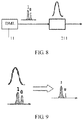
- a chirping characteristic of a DML causes that a wavelength of the DML is different for different injected currents, where an emergent wavelength of the DML for a "1" signal is generally slightly shorter than an emergent wavelength of the DML for a "0" signal.
- FIG. 8 is a schematic diagram of outputting an optical signal by a DML.
- FIG. 9 is a schematic diagram of an optical signal that is output by a DML and that is coupled to the second waveguide 23 by a circular waveguide.
- An MPD2 can detect a strength of optical signals coupled from the circular waveguide group 21 corresponding to the MPD2, and an MPD1 can detect a strength of optical signals output by the DML, in the optical transmitter, that is corresponding to the MPD1, and the foregoing two strengths have a preset strength ratio.
- a feedback control circuit 30 increases a current input into the heating electrode in the circular waveguide group 21 corresponding to the feedback control circuit 30, so that the resonant wavelength of the circular waveguide group 21 shifts toward a long-wavelength direction; when the ratio of the foregoing two strengths is less than the preset strength ratio, the feedback control circuit 30 decreases the current input into the heating electrode in the circular waveguide group 21 corresponding to the feedback control circuit 30, so that the resonant wavelength of the circular waveguide group 21 shifts toward a short-wavelength direction.
- each circular waveguide group 21 includes one circular waveguide 211, but in an actual application, two or more circular waveguides 211 may be used in the circular waveguide group 21 to achieve a better filtering effect.
- two circular waveguides 211 may be provided in each circular waveguide group 21.
- FIG. 10 is another schematic structural diagram of an optical transmitter according to an embodiment of the present invention.
- the micro-ring group array in this embodiment of the present invention implements not only filtering but also multiplexing, which effectively reduces a quantity of elements, reduces a size of an optical transmitter, and reduces costs.
- the present invention further uses a control component to control a resonant wavelength of a circular waveguide group, which ensures an optimum operating state of the circular waveguide group, and thereby ensures that the entire optical transmitter operates in an optimum state.
- a heating electrode is provided in the circular waveguide group.
- the micro-ring group array implements photo-electricity integration, which further reduces the size of the optical transmitter, and effectively reduces power consumption.
- this embodiment of the present invention further provides an optical transmission method, which may be specifically as follows:
- FIG. 11 is a flowchart of the optical transmission method in this embodiment of the present invention, where specific steps may be as follows:
- Each first waveguide is coupled with one side of a corresponding circular waveguide group, and each first waveguide includes a first port and a second port.
- N directly modulated lasers, N circular waveguide groups, and N first waveguides form N optical transmission components, where each optical transmission component consists of one directly modulated laser, one circular waveguide group, and one first waveguide, the circular waveguide group includes at least one circular waveguide, and N is greater than or equal to 2.
- the micro-ring group array may include four circular waveguide groups, four first waveguides, and one second waveguide 23, one circular waveguide group includes one circular waveguide, and each optical transmission component includes one DML, one circular waveguide, and one first waveguide.
- an optical transmission component when a distance between a circular waveguide and a first waveguide is relatively small, an optical signal transmitted in the first waveguide is coupled to the circular waveguide, and similarly, an optical signal transmitted in the circular waveguide is also coupled to the first waveguide.
- an optical signal transmitted in the circular waveguide is coupled to the second waveguide.
- the circular waveguide group couples a part of optical signals in optical signals from the first waveguide corresponding to the circular waveguide group to a second waveguide, where an extinction ratio of the part of optical signals coupled to the second waveguide is greater than an extinction ratio of the optical signals from the first waveguide corresponding to the circular waveguide group.
- each circular waveguide group is coupled with a first waveguide corresponding to the circular waveguide group, and the other side is coupled with the second waveguide.
- Wavelengths of the part of optical signals in the optical signals from the first waveguide corresponding to the circular waveguide group fall within a preset range of a resonant wavelength of the circular waveguide group, where resonant wavelengths of circular waveguides in each circular waveguide group are equal.
- the second waveguide aggregates optical signals from circular waveguide groups, and outputs the aggregated optical signals.
- step may further be included: coupling, by the circular waveguide group, a remaining part of optical signals in the optical signals from the first waveguide corresponding to the circular waveguide group to the second port, which, for example, may be as follows:
- a first waveguide is used to receive, through a first port, an optical signal output by a directly modulated laser corresponding to the first waveguide, and couple the received optical signal to a circular waveguide group corresponding to the first waveguide, and the circular waveguide group couples a part of optical signals in optical signals from the first waveguide corresponding to the circular waveguide group to a second waveguide, where an extinction ratio of the part of optical signals coupled to the second waveguide is greater than an extinction ratio of the optical signals from the first waveguide corresponding to the circular waveguide group, and the second waveguide aggregates optical signals from circular waveguide groups, and outputs the aggregated optical signals.
- filtering but also multiplexing are implemented, which effectively reduces a quantity of elements, reduces a size of an optical transmitter, and reduces costs.
Landscapes
- Physics & Mathematics (AREA)
- Electromagnetism (AREA)
- Engineering & Computer Science (AREA)
- Computer Networks & Wireless Communication (AREA)
- Signal Processing (AREA)
- Optics & Photonics (AREA)
- Optical Modulation, Optical Deflection, Nonlinear Optics, Optical Demodulation, Optical Logic Elements (AREA)
- Optical Integrated Circuits (AREA)
- Optical Communication System (AREA)
Description
- The present invention relates to the communications field, and in particular, to an optical transmitter and an optical transmission method.
- Restricted by a chirping characteristic of a directly modulated laser (DML, Directly Modulated Laser), in an optical communications system that supports high-speed (speed higher than 10 Gbps) and long-distance transmission (distance greater than 20 Km), the DML cannot be directly used as an optical transmission source. With a high-speed and large-capacity development trend for an optical network, advantages of low costs and low power consumption are increasingly attractive, and the DML has advantages of low costs and low power consumption.
- In an existing technical solution, generally a filter is added after a DML of an optical communications system for performing spectrum shaping on an output signal of the DML, achieving purposes of controlling chirping and increasing a transmission distance.
- In the prior art, however, this is mostly implemented by using a method of using discrete elements, where single-function optical elements are optically coupled by using free space. For example, a multi-cavity filter is added after a DML to implement conversion from a frequency-modulated signal to an amplitude-modulated signal, so as to achieve purposes of increasing a signal extinction ratio, controlling chirping, and implementing long distance transmission. In this implementation method, discrete elements are used; therefore, a size of an optical module is relatively large and integration is not convenient. Multiple discrete elements increase difficulty in coupling and packaging, and increase costs of coupling and packaging. If this solution is to be applied to a multi-channel transmitter, a functional element for wavelength division multiplexing further needs to be added, which further increases the size of the optical module.
-
US8611747B1 describes that an optical waveguide can transmit multiple optical signals imprinted or encoded with different information, thereby increasing the waveguide's information carrying capability or bandwidth. Each optical signal can comprise multiple longitudinal modes that are energized and that are modulated substantially in unison. Thus, the photonic energy of each optical signal can be spread across a wavelength region in a substantially discrete or substantially discontinuous pattern. The respective wavelength regions of the optical signals can overlap or substantially overlay one another. Modes of one of the optical signals can be substantially interleaved, interspersed, or intermingled with modes of other optical signals. Systems at ends of the optical waveguide can feed the optical signals onto and off of the optical waveguide and discriminate the optical signals from one another. The systems can comprise ring resonators. The waveguide can support an on-chip network, such as for a multicore processor of a computer. -
EP1786121A1 describes that in an optical transmitter comprising a directly modulated laser and a wavelength filter provided on a post-stage of the directly modulated laser, the wavelength filter has a modulated light input port for inputting modulated light output from the directly modulated laser, a filter transmitted light output port for outputting light having a wavelength included in a filter transmission band among the modulated light as filter transmitted light, and a filter cutoff light output port provided separately from the modulated light input port and the filter transmitted light output port and outputting light having a wavelength included in a filter cutoff band among the modulated light as filter cutoff light, and the peak of the filter transmission band is set on a shorter-wave side from the peak of the spectrum of modulated light output from the directly modulated laser. - Embodiments of the present invention provide an optical transmitter and an optical transmission method, which are applicable to multi-channel transmission and can effectively reduce a size of an optical transmitter.
- According to a first aspect, the present invention provides an optical transmitter, including a directly modulated laser array and a micro-ring group array, where the directly modulated laser array includes N directly modulated lasers, and the micro-ring group array includes N circular waveguide groups, N first waveguides, and one second waveguide, where the N directly modulated lasers, the N circular waveguide groups, and the N first waveguides form N optical transmission components, each optical transmission component consists of one directly modulated laser, one circular waveguide group, and one first waveguide, the circular waveguide group includes at least one circular waveguide, and N is greater than or equal to 2;
- each directly modulated laser is configured to output an optical signal, where wavelengths of optical signals output by the directly modulated lasers are different from each other;
- each first waveguide is coupled with one side of a corresponding circular waveguide group, each first waveguide includes a first port and a second port, and each first waveguide is configured to receive, through the first port, an optical signal output by a directly modulated laser corresponding to the first waveguide, and couple the received optical signal to the circular waveguide group corresponding to the first waveguide;
- one side of each circular waveguide group is coupled with a first waveguide corresponding to the circular waveguide group, and the other side is coupled with the second waveguide, and each circular waveguide group is configured to couple a part of optical signals from the first waveguide corresponding to the circular waveguide group to the second waveguide, where an extinction ratio of the part of optical signals that are coupled to the second waveguide is greater than an extinction ratio of the optical signals from the first waveguide corresponding to the circular waveguide group; and
- the second waveguide is configured to aggregate optical signals from the circular waveguide groups, and output an aggregated optical signals.
- The optical transmitter further includes N control components, where each control component is corresponding to one optical transmission component;
- each control component includes one first monitor photo detector, one second monitor photo detector, and one feedback control circuit;
- the circular waveguide group is further configured to couple a remaining part of optical signals in the optical signals from the first waveguide corresponding to the circular waveguide group to the second port;
- each first monitor photo detector is configured to detect a strength of optical signals output by a directly modulated laser corresponding to the first monitor photo detector in the optical transmitter, and input a detection result into a corresponding feedback control circuit;
- each second monitor photo detector is connected to a second port of a first waveguide corresponding to the second monitor photo detector, and the second monitor photo detector is configured to detect a strength of the remaining part of optical signals, and input a detection result into the corresponding feedback control circuit; and
- the feedback control circuit is configured to control a resonant wavelength of the circular waveguide group according to the detection results input by the first monitor photo detector and the second monitor photo detector.
- According to the first aspect, in a second possible implementation manner, a heating electrode is provided in each circular waveguide group; and
- the feedback control circuit is further configured to:
- control the resonant wavelength of the circular waveguide group by controlling a current input into a heating electrode in the circular waveguide group corresponding to the feedback control circuit.
- According to the second possible implementation manner of the first aspect, in a third possible implementation manner, the feedback control circuit is further configured to: when a strength ratio is greater than a preset strength ratio, increase the current input into the heating electrode in the circular waveguide group corresponding to the feedback control circuit, where the strength ratio is a ratio of the strength of optical signals detected by the first monitor photo detector corresponding to the feedback control circuit to the strength of optical signals detected by the second monitor photo detector corresponding to the feedback control circuit; and when the strength ratio is less than the preset strength ratio, decrease the current input into the heating electrode in the circular waveguide group corresponding to the feedback control circuit.
- According to the first aspect, or the first possible implementation manner, the second possible implementation manner, or the third possible implementation manner of the first aspect, in a fourth possible implementation manner,
- wavelengths of the part of optical signals that are coupled to the second waveguide by each circular waveguide group fall within a preset range of the resonant wavelength of the circular waveguide group, where resonant wavelengths of circular waveguides in each circular waveguide group are equal.
- According to a second aspect, the present invention provides an optical transmission method, including:
- receiving, by a first waveguide through a first port, an optical signal output by a directly modulated laser corresponding to the first waveguide, and coupling the received optical signal to a circular waveguide group corresponding to the first waveguide, where each first waveguide is coupled with one side of a corresponding circular waveguide group, each first waveguide includes a first port and a second port, and N directly modulated lasers, N circular waveguide groups, and N first waveguides form N optical transmission components, where each optical transmission component consists of one directly modulated laser, one circular waveguide group, and one first waveguide, the circular waveguide group includes at least one circular waveguide, and N is greater than or equal to 2;
- coupling, by the circular waveguide group, a part of optical signals from the first waveguide corresponding to the circular waveguide group to a second waveguide, where an extinction ratio of the part of optical signals coupled to the second waveguide is greater than an extinction ratio of the optical signals from the first waveguide corresponding to the circular waveguide group, where one side of each circular waveguide group is coupled with a first waveguide corresponding to the circular waveguide group, and the other side is coupled with the second waveguide; and
- aggregating, by the second waveguide, optical signals from the circular waveguide groups, and outputting an aggregated optical signals.
- The circular waveguide group couples a remaining part of optical signals in the optical signals from the first waveguide corresponding to the circular waveguide group to the second port, so that a feedback control circuit controls a resonant wavelength of the circular waveguide group according to a strength of the remaining part of optical signals that is detected by a second monitor photo detector corresponding to the feedback control circuit and a strength of the part of optical signals that is detected by a first monitor photo detector, where each circular waveguide group is corresponding to one first monitor photo detector, one second monitor photo detector, and one feedback control circuit, and each second monitor photo detector is connected to a second port of a first waveguide corresponding to the second monitor photo detector.
- According to the second aspect, or the first possible implementation manner of the second aspect, in a second possible implementation manner, wavelengths of the part of optical signals in the optical signals from the first waveguide corresponding to the circular waveguide group fall within a preset range of the resonant wavelength of the circular waveguide group, where resonant wavelengths of circular waveguides in each circular waveguide group are equal.
- It can be seen from the foregoing technical solutions that the embodiments of the present invention have the following advantages:
- In the embodiments of the present invention, a directly modulated laser array is used to implement multi-channel transmission, where each directly modulated laser is correspondingly provided with one circular waveguide group and one first waveguide, each circular waveguide group may couple a part of optical signals output by a directly modulated laser corresponding to the circular waveguide group to a same second waveguide, and the second waveguide aggregates optical signals from circular waveguide groups and outputs the aggregated optical signals, which effectively reduces a quantity of elements, reduces a size of an optical transmitter, and reduces costs.
- To describe the technical solutions in the embodiments of the present invention more clearly, the following briefly introduces the accompanying drawings required for describing the embodiments. Apparently, the accompanying drawings in the following description show merely some embodiments of the present invention, and a person skilled in the art may still derive other drawings from these accompanying drawings without creative efforts.
-
FIG. 1 is a schematic structural diagram of an optical transmitter according to an embodiment of the present invention; -
FIG. 2 is a schematic structural diagram of a circular waveguide group according to an embodiment of the present invention; -
FIG. 3 is a schematic structural diagram of a circular waveguide group and a control component according to an embodiment of the present invention; -
FIG. 4 is a schematic structural diagram of one micro-ring group of a micro-ring group array according to an embodiment of the present invention; -
FIG. 5 is another schematic structural diagram of one micro-ring group of a micro-ring group array according to an embodiment of the present invention; -
FIG. 6 is a schematic structural diagram of a micro-ring group array according to an embodiment of the present invention; -
FIG. 7 is a schematic diagram of a filtering characteristic curve of a circular waveguide according to an embodiment of the present invention; -
FIG. 8 is a schematic diagram of outputting an optical signal by a directly modulated laser according to an embodiment of the present invention; -
FIG. 9 is a schematic diagram of an optical signal that is output by a directly modulated laser and that is coupled to a second waveguide by a circular waveguide according to an embodiment of the present invention; -
FIG. 10 is another schematic structural diagram of an optical transmitter according to an embodiment of the present invention; and -
FIG. 11 is a flowchart of an optical transmission method according to an embodiment of the present invention. - The following clearly and completely describes the technical solutions in the embodiments of the present invention with reference to the accompanying drawings in the embodiments of the present invention. Apparently, the described embodiments are merely some but not all of the embodiments of the present invention. All other embodiments obtained by a person skilled in the art based on the embodiments of the present invention without creative efforts shall fall within the protection scope of the present invention.
- The embodiments of the present invention provide an optical transmitter, which is applicable to multi-channel transmission, and can effectively reduce a size of an optical transmitter and reduce costs, and in addition, further provide a corresponding optical transmission method. Referring to
FIG. 1 to FIG. 11 , detailed descriptions are given below respectively. - This embodiment of the present invention provides an optical transmitter, which is applicable to a high-speed, long-distance transmission optical communication system. Referring to
FIG. 1, FIG. 1 is a schematic structural diagram of an optical transmitter according to this embodiment of the present invention, which may be specifically as follows: - An optical transmitter includes a directly modulated laser array 10 and a micro-ring group array 20, where the directly modulated laser array 10 includes N directly modulated lasers 11, and the micro-ring group array 20 includes N circular waveguide groups 21, N first waveguides 22, and one second waveguide 23, where the N directly modulated lasers 11, the N circular waveguide groups 21, and the N first waveguides 22 form N optical transmission components, each optical transmission component consists of one directly modulated laser 11, one circular waveguide group 21, and one first waveguide 22, the circular waveguide group 21 includes at least one circular waveguide 211, and N is greater than or equal to 2; each directly modulated laser 11 is configured to output an optical signal, where wavelengths of optical signals output by the directly modulated lasers 11 are different from each other; each first waveguide 22 is coupled with one side of a corresponding circular waveguide group 21, each first waveguide 22 includes a first port 221 and a second port 222, and each first waveguide 22 is configured to receive, through the first port 221, an optical signal output by a directly modulated laser 11 corresponding to the first waveguide 22, and couple the received optical signal to the circular waveguide group 21 corresponding to the first waveguide 22; one side of each circular waveguide group 21 is coupled with a first waveguide 22 corresponding to the circular waveguide group 21, and the other side is coupled with the second waveguide 23, and each circular waveguide group 21 is configured to couple a part of optical signals in optical signals from the first waveguide 22 corresponding to the circular waveguide group 21 to the second waveguide 23, where an extinction ratio of the part of optical signals that are coupled to the second waveguide 23 is greater than an extinction ratio of the optical signals from the first waveguide 22 corresponding to the circular waveguide group 21; and the second waveguide 23 is configured to aggregate optical signals from the circular waveguide groups 21, and output the aggregated optical signals.
- The directly modulated
laser array 10 in this embodiment of the present invention may include N directly modulated lasers 11 (DML, Directly Modulated Laser), where N is greater than or equal to 2. Each DML in the directly modulatedlaser array 10 may output an optical signal into themicro-ring group array 20, and wavelengths of optical signals output by the DMLs are different from each other. - The
micro-ring group array 20 in this embodiment of the present invention may receive optical signals output by the directly modulatedlaser array 10, aggregate a part of optical signals in the optical signals received from the DMLs, and output the aggregated optical signals. Themicro-ring group array 20 may include Ncircular waveguide groups 21, N first waveguides 22, and onesecond waveguide 23, where N is greater than or equal to 2, and acircular waveguide group 21 may include at least onecircular waveguide 211. - In the optical transmitter in this embodiment of the present invention, the N directly modulated
lasers 11, the Ncircular waveguide groups 21, and the Nfirst waveguides 22 form the N optical transmission components, where N is greater than or equal to 2, and each optical transmission component consists of one directly modulatedlaser 11, onecircular waveguide group 21, and onefirst waveguide 22. Eachfirst waveguide 22 is coupled with one side of a correspondingcircular waveguide group 21, eachfirst waveguide 22 includes afirst port 221 and asecond port 222, one side of eachcircular waveguide group 21 is coupled with afirst waveguide 22 corresponding to thecircular waveguide group 21, and the other side is coupled with thesecond waveguide 23. - In each optical transmission component, a directly modulated
laser 11 outputs an optical signal into afirst waveguide 22 corresponding to the directly modulatedlaser 11, thefirst waveguide 22 receives the optical signal through afirst port 221, and couples the received optical signal to acircular waveguide group 21 corresponding to thefirst waveguide 22, thecircular waveguide group 21 couples a part of optical signals in optical signals from thefirst waveguide 22 to thesecond waveguide 23, where an extinction ratio of the part of optical signals coupled to thesecond waveguide 23 is greater than an extinction ratio of optical signals that are received by thefirst waveguide 22 through thefirst port 221. - The
second waveguide 23 may aggregate optical signals that are coupled by thecircular waveguide groups 21 in the optical transmission components, and output the aggregated optical signals to a transmission port of the optical transmitter. - It can be known from the above that, in this embodiment of the present invention, a directly modulated laser array is used to implement multi-channel transmission, where each directly modulated laser is correspondingly provided with one circular waveguide group and one first waveguide, each circular waveguide group may couple a part of optical signals output by a directly modulated laser corresponding to the circular waveguide group to a same second waveguide, and the second waveguide aggregates optical signals from circular waveguide groups and outputs the aggregated optical signals. The micro-ring group array implements not only filtering but also multiplexing, which effectively reduces a quantity of elements, reduces a size of an optical transmitter, and reduces costs.
- On the basis of Embodiment 1, this embodiment of the present invention may further include a control component, where the control component may control a resonant wavelength of the
circular waveguide group 21. Referring toFIG. 1, FIG. 1 is a schematic structural diagram of an optical transmitter according to this embodiment of the present invention, which may be specifically as follows: - Generally, a refractive index of the
circular waveguide group 21 changes with a temperature. When a temperature of thecircular waveguide group 21 changes, the refractive index of thecircular waveguide group 21 changes, and therefore the resonant wavelength of thecircular waveguide group 21 also changes. This phenomenon is known as the thermo-optic effect. In an actual application, both a wavelength of a DML and the resonant wavelength of thecircular waveguide group 21 change with a change in the environment, such as an operating temperature. In order to avoid that thecircular waveguide group 21 cannot couple an optical signal output by the DML to thesecond waveguide 23 because the resonant wavelength of thecircular waveguide group 21 changes due to occurrence of the thermo-optic effect, in this embodiment of the present invention, a control component may be provided to control the resonant wavelength of thecircular waveguide group 21, so that the resonant wavelength of thecircular waveguide group 21 falls within a wavelength range of the optical signal output by the DML. For example, it may be specifically as follows:- The optical transmitter in this embodiment of the present invention may further include N control components, where each control component is corresponding to one optical transmission component; each control component includes one
feedback control circuit 30 and two monitor photo detectors (MPD, Monitor Photo Detector). For ease of description, the two monitor photo detectors may be respectively described as a first monitor photo detector 40 (MPD1) and a second monitor photo detector 50 (MPD2). The two MPDs may respectively detect a strength of optical signals output by a DML and a strength of optical signals that are coupled to asecond port 222 by acircular waveguide group 21. For example, it may be specifically as follows:- Each MPD1 is configured to detect a strength of optical signals output by a DML corresponding to the MPD1 in the optical transmitter, obtain a detection result, and input the detection result into a corresponding
feedback control circuit 30. It should be noted that, each DML has two end faces, where one end face is configured to output optical signals to an MPD1, and the MPD1 detects power of the optical signals output by this end face, and the other end face is configured to output optical signals to afirst port 221 of afirst waveguide 22. Output power of the optical signals output by the two end faces of the DML is in a proportional relationship, and the output power is in direct proportion to reflectivity of the end face of the DML. For each DML, the two end faces have preset reflectivity, where reflectivity of one end face is far greater than reflectivity of the other end face, and because of characteristics of the MPD1 and thefirst waveguide 22, a proportion of optical signals output to thefirst port 221 is inevitably far greater than that of optical signals output to the MPD1. It can be known from Embodiment 1 that, eachcircular waveguide group 21 may couple a part of optical signals in optical signals from afirst waveguide 22 corresponding to thecircular waveguide group 21 to thesecond waveguide 23. In addition, thecircular waveguide group 21 may also couple a remaining part of optical signals in the optical signals from thefirst waveguide 22 corresponding to thecircular waveguide group 21 to asecond port 222. Each MPD2 is connected to asecond port 222 of afirst waveguide 22 corresponding to the MPD2. That is, an optical signal transmitted by a DML may have the following transmission paths:- DML→first waveguide→circular waveguide→second port; and
- DML→first waveguides→circular waveguides→second waveguide.
- Each MPD1 is configured to detect a strength of optical signals output by a DML corresponding to the MPD1 in the optical transmitter, obtain a detection result, and input the detection result into a corresponding
- The optical transmitter in this embodiment of the present invention may further include N control components, where each control component is corresponding to one optical transmission component; each control component includes one
- An extinction ratio of the optical signals that are coupled to the second waveguide by the circular waveguide is greater than an extinction ratio of optical signals that are coupled from the first waveguide. It should be noted that, wavelengths of the part of optical signals coupled to the
second waveguide 23 fall within a range of a resonant wavelength of thecircular waveguide group 21, where resonant wavelengths ofcircular waveguides 211 in eachcircular waveguide group 21 are equal. The wavelengths of the part of optical signals coupled to thesecond waveguide 23 have a preset range, which is specifically described in detail in the following embodiments, and is not described herein. - Each MPD2 is configured to detect a strength of a remaining part of optical signals coupled by the
circular waveguide group 21 corresponding to the MPD2, obtain a detection result, and input the detection result into the correspondingfeedback control circuit 30. - The
feedback control circuit 30 is configured to control the resonant wavelength of thecircular waveguide group 21 according to the detection results input by the foregoing MPD1 and MPD2. - Specifically, the
feedback control circuit 30 may control the resonant wavelength of thecircular waveguide group 21 in the following manner: - A
heating electrode 212 may be provided in thecircular waveguide group 21. Referring toFIG. 2, FIG. 2 is a schematic structural diagram of a circular waveguide group.FIG. 3 is a schematic structural diagram of a circular waveguide group and a control component, where thecircular waveguide group 21 includes onecircular waveguide 211. If thecircular waveguide group 21 includes two or morecircular waveguides 211, one heating electrode may be provided in thecircular waveguide group 21, or one heating electrode may be separately provided in eachcircular waveguide 211, and the heating electrode on eachcircular waveguide 211 is controlled by using a same feedback control circuit, so as to ensure that currents input intocircular waveguides 211 in the samecircular waveguide group 21 are equal in magnitude. - The
heating electrode 212 is provided in thecircular waveguide group 21, and thefeedback control circuit 30 may control a temperature of thecircular waveguide group 21 by controlling a current input into theheating electrode 212 in thecircular waveguide group 21 corresponding to thefeedback control circuit 30, and adjust an effective refractive index of thecircular waveguide group 21, so as to control the resonant wavelength of thecircular waveguide group 21. - The
feedback control circuit 30 may acquire in advance magnitude of photocurrents input into the feedback control circuit by the MPD1 and the MPD2 that are corresponding to thefeedback control circuit 30, and magnitude of the current loaded on theheating electrode 212 in thecircular waveguide group 21 corresponding to thefeedback control circuit 30. Thefeedback control circuit 30 may perform a division operation on the foregoing acquired magnitude of the photocurrents input into thefeedback control circuit 30 by the MPD1 and the MPD2 to obtain a ratio, where in this embodiment, the ratio may be described as a preset strength ratio. Because both the resonant wavelength of thecircular waveguide group 21 and a wavelength of an optical signal output by the DML have distributions, when external environment changes, it causes that an offset occurs between the resonant wavelength of thecircular waveguide group 21 and the wavelength of the optical signal output by the DML. When an optimum operating state is departed, the ratio of the photocurrents input into thefeedback control circuit 30 by the MPD1 and MPD2 changes, in which case thefeedback control circuit 30 may learn that the ratio has changed, so as to control the resonant wavelength of thecircular waveguide group 21. For example, it may be specifically as follows: - The MPD1 and the MPD2 may detect a strength of optical signals, and send detection results to the
feedback control circuit 30 by using a photocurrent signal, the foregoing photocurrent signal is used as a feedback input signal for thefeedback control circuit 30, and thefeedback control circuit 30 may output a control signal according to the received photocurrent signal to control the resonant wavelength of thecircular waveguide group 21. Then it can be learned, from a ratio of the strength of optical signals that is detected by the MPD1 to the strength of optical signals that is detected by the MPD2, whether an offset occurs between the resonant wavelength of thecircular waveguide group 21 and the wavelength of the optical signal output by the DML. - Assuming that the ratio of the strength of optical signals that is detected by the MPD1 to the strength of optical signals that is detected by the MPD2 is a strength ratio S, where the MPD1 and the MPD2 are corresponding to the
feedback control circuit 30, when S is greater than the preset strength ratio, it is indicated that optical signals that are coupled to thesecond port 222 of thefirst waveguide 22 by thecircular waveguide group 21 are excessively strong, and optical signals that are coupled to thesecond waveguide 23 by thecircular waveguide group 21 are excessively weak, that is, the resonant wavelength of thecircular waveguide group 21 is excessively small relative to the output wavelength of the DML. In this case, thefeedback control circuit 30 increases the current input into theheating electrode 212 in thecircular waveguide group 21 corresponding to thefeedback control circuit 30, so that the resonant wavelength of thecircular waveguide group 21 shifts toward a long-wavelength direction to ensure an optimum operating state of thecircular waveguide group 21. - When S is less than the preset strength ratio, the
feedback control circuit 30 decreases the current input into the heating electrode in thecircular waveguide group 21 corresponding to thefeedback control circuit 30, so that the resonant wavelength of thecircular waveguide group 21 shifts toward a short-wavelength direction, ensuring that the entire optical transmitter operates in an optimum state. - When S is equal to the preset strength ratio, it is indicated that the
circular waveguide group 21 is in a normal operating state, and a part of optical signals in optical signals from thefirst waveguide 22 corresponding to thecircular waveguide group 21 may be coupled to thesecond waveguide 23, and a remaining part of optical signals are coupled to thesecond port 222 of thefirst waveguide 22, where an extinction ratio of the part of optical signals coupled to thesecond waveguide 23 is greater than an extinction ratio of the optical signals from thefirst waveguide 22 corresponding to thecircular waveguide group 21, and wavelengths of the part of optical signals coupled to thesecond waveguide 23 fall within a preset range of the resonant wavelength of thecircular waveguide group 21. - It can be known from the above that, in this embodiment of the present invention, a directly modulated laser array is used to implement multi-channel transmission, where each directly modulated laser is correspondingly provided with one circular waveguide group and one first waveguide, each circular waveguide group may couple a part of optical signals output by a directly modulated laser corresponding to the circular waveguide group to a same second waveguide, and the second waveguide aggregates optical signals from circular waveguide groups and outputs the aggregated optical signals. The micro-ring group array implements not only filtering but also multiplexing, which effectively reduces a quantity of elements, reduces a size of an optical transmitter, and reduces costs. Further, a control component is also used to control a resonant wavelength of the circular waveguide group, which ensures an optimum operating state of the circular waveguide group, and thereby ensures that the entire optical transmitter operates in an optimum state. A heating electrode is provided in the circular waveguide group. The micro-ring group array implements photo-electricity integration, which further reduces the size of the optical transmitter, and effectively reduces power consumption.
- The following describes in detail an optical transmitter in this embodiment of the present invention by using a specific application example. The optical transmitter includes four optical transmission components, and each
circular waveguide group 21 includes onecircular waveguide 211. Specifically, reference may be made toFIG. 1 , whereFIG. 1 is a schematic structural diagram of the optical transmitter in this embodiment of the present invention. - The
micro-ring group array 20 includes fourcircular waveguide groups 21, fourfirst waveguides 22, and onesecond waveguide 23, onecircular waveguide group 21 includes onecircular waveguide 211, and each optical transmission component includes one DML, onecircular waveguide 211, and onefirst waveguide 22. In an optical transmission component, when a distance between acircular waveguide 211 and afirst waveguide 22 is relatively small, an optical signal transmitted in thefirst waveguide 22 is coupled to thecircular waveguide 211, and similarly, an optical signal transmitted in thecircular waveguide 211 is also coupled to thefirst waveguide 22. Similarly, when a distance between thecircular waveguide 211 and thesecond waveguide 23 is relatively small, an optical signal transmitted in thecircular waveguide 211 is coupled to thesecond waveguide 23. Referring toFIG. 4 ,FIG. 5, and FIG. 6 ,FIG. 4 is a schematic structural diagram of one micro-ring group of a micro-ring group array,FIG. 5 is another schematic structural diagram of one micro-ring group of a micro-ring group array, andFIG. 6 is a schematic structural diagram of a micro-ring group array. It should be noted that, aheating electrode 212 is not shown inFIG. 6 , but thecircular waveguide group 21 may be provided with a heating electrode in practice. - As shown in
FIG. 5, FIG. 5 is another schematic structural diagram of one micro-ring group of a micro-ring group array. Each micro-ring group has two coupling regions, which are Z1 and Z2 respectively. When coupled in the coupling regions, an optical signal shifts
laser 11 corresponding to afirst waveguide 22 and that is received by thefirst waveguide 22 through afirst port 221 is λ, and the optical signal whose wavelength is λ is coupled to acircular waveguide 211, and after transmission in thecircular waveguide 211 for one circle, a phase change is shown in an equation (1):
circular waveguide 211, where magnitude of β is equal to a transmission constant
- When θ = 2mπ (where m is an integer), after traveling in the
circular waveguide 211 for one circle, the optical signal returns to the coupling region Z1 for thefirst waveguide 22, and a total phase change, inclusive of phase shifts occurring in the two coupling regions Z1 and Z2, that is undergone by the optical signal during the traveling for one circle is (2m+1)π ; therefore, when the optical signal returns to the coupling region Z1 after traveling for one circle, destructive interference occurs between the optical signal and an optical signal received through thefirst port 221 from the DML, so that after traveling for one circle, most optical signals are coupled back to thecircular waveguide 211, and so on. In the coupling region Z2, thecircular waveguide 211 couples a part of optical signals in optical signals from thefirst waveguide 22 corresponding to thecircular waveguide 211 to thesecond waveguide 23 for outputting. - It can be known from the equation (1) that θ is related to λ; therefore, a degree of destructive interference at the coupling region Z1 are different for light of different wavelengths, resulting that optical energy allocated to the
second port 222 and thesecond waveguide 23 is different for optical signals of different wavelengths, which presents a filtering characteristic curve shown inFIG. 7. FIG. 7 is a schematic diagram of a filtering characteristic curve of a circular waveguide, where a solid line inFIG. 7 indicates optical signals allocated to the second port, and a dashed line indicates optical signals allocated to the second waveguide. - It can be known from
FIG. 7 that the filtering characteristic curve of thecircular waveguide 211 presents a periodic distribution, which is because when m in θ = 2mπ (where m is an integer) takes different values, a wavelength is correspondingly different, where a wavelength that makes θ = 2mπ true may be referred to as a resonant wavelength, and only an optical signal with a wavelength near a resonant wavelength may be coupled to thesecond waveguide 23 and output. An optical signal with a wavelength near a resonant wavelength is an optical signal in a preset range. - As shown
FIG. 6, FIG. 6 is a schematic structural diagram of a micro-ring group array. In themicro-ring group array 20, in each optical transmission component, afirst waveguide 22 receives, through afirst port 221, an optical signal output by a DML corresponding to thefirst waveguide 22, and couples all optical signals to acircular waveguide 211 corresponding to thefirst waveguide 22. For ease of description,circular waveguides 211 are described as a first circular waveguide, a second circular waveguide, a third circular waveguide, and a fourth circular waveguide from left to right. Assuming that thefirst waveguide 22 receives, through thefirst port 221, an optical signal whose wavelength is λ1 that is output by the DML corresponding to thefirst waveguide 22, and couples all optical signals whose wavelengths are λ1 to the first circular waveguide. Assuming that a resonant wavelength of the first circular waveguide is λ' 1, the first circular waveguide may couple an optical signal whose wavelength is λ' 1 to thesecond waveguide 23. Similarly, in another optical transmission component, assuming that afirst waveguide 22 couples all optical signals whose wavelengths are λ 2 to the second circular waveguide, and assuming that a resonant wavelength of the second circular waveguide is λ' 2, the second circular waveguide may couple an optical signal whose wavelength is λ ' 2 in the optical signals whose wavelengths are λ 2 to thesecond waveguide 23, and in a same way, the third circular waveguide may couple an optical signal whose wavelength is λ ' 3 to thesecond waveguide 23, and the fourth circular waveguide may couple an optical signal whose wavelength is λ ' 4 to thesecond waveguide 23. Because the resonant wavelengths of the first circular waveguide and the second circular waveguide are different, when traveling through a coupling region for the second circular waveguide and thesecond waveguide 23, the optical signal whose wavelength is λ' 1 is not interfered by the second circular waveguide, and may be directly output from thesecond waveguide 23, and similarly, when traveling through a coupling region for the third circular waveguide and thesecond waveguide 23, the optical signal whose wavelength is λ' 2 is not interfered by the third circular waveguide, and may be directly output from thesecond waveguide 23, and in a same way, thesecond waveguide 23 may output optical signals whose wavelengths are λ' 1, λ' 2, λ' 3, and λ' 4 that are coupled by the first circular waveguide, the second circular waveguide, the third circular waveguide, and the fourth circular waveguide. - In an actual application, in order to avoid that an inevitable situation causes an error of the resonant wavelength of the circular waveguide, the
circular waveguide group 21 may be so set that thecircular waveguide group 21 couples an optical signal falling within a preset range of a resonant wavelength of thecircular waveguide group 21 to thesecond waveguide 23. For example, the first circular waveguide, the second circular waveguide, the third circular waveguide, and the fourth circular waveguide may couple optical signals whose wavelengths are λ' 1 +C, λ' 2 +C, λ' 3 +C, and λ' 4+C to thesecond waveguide 23, where C is a constant, and C has a relatively small range. - Because only an optical signal with a wavelength near the resonant wavelength may be coupled to the
second waveguide 23, thecircular waveguide group 21 has a quite good filtering function. In this embodiment of the present invention, differentcircular waveguide groups 21 are coupled with the samesecond waveguide 23 at one side, and because resonant wavelengths of thecircular waveguide groups 21 in the optical transmitter are different from each other, wavelengths of optical signals coupled to thesecond waveguide 23 are different, and thesecond waveguide 23 may aggregate optical signals with different wavelengths that are coupled by thecircular waveguide groups 21, which implements a multiplexing function, reduces a quantity of devices, and implements miniaturization of a device. - An extinction ratio of the part of optical signals that are coupled to the
second waveguide 23 by thecircular waveguides 211 is greater than an extinction ratio of optical signals coupled from thefirst waveguides 22 corresponding to thecircular waveguides 211. - In a case of direct modulation, a chirping characteristic of a DML causes that a wavelength of the DML is different for different injected currents, where an emergent wavelength of the DML for a "1" signal is generally slightly shorter than an emergent wavelength of the DML for a "0" signal. Specifically, reference may be made to
FIG. 8 , whereFIG. 8 is a schematic diagram of outputting an optical signal by a DML. When wavelengths of optical signals output by the DML fall at a falling edge of acircular waveguide 211, most "1" signals are not filtered out, while most "0" signals are filtered out. Therefore, after optical signals received through afirst port 221 travel through thecircular waveguide 211, an energy ratio of "1" signals to "0" signals becomes greater, that is, an extinction ratio increases. Specifically, reference may be made toFIG. 9, FIG. 9 is a schematic diagram of an optical signal that is output by a DML and that is coupled to thesecond waveguide 23 by a circular waveguide. - When environment, such as an operating temperature, changes, both a wavelength of an optical signal output by the DML and a resonant wavelength of a
circular waveguide group 21 change, and when the resonant wavelength of thecircular waveguide group 21 changes, magnitude of a current in a heating electrode in thecircular waveguide group 21 changes. An MPD2 can detect a strength of optical signals coupled from thecircular waveguide group 21 corresponding to the MPD2, and an MPD1 can detect a strength of optical signals output by the DML, in the optical transmitter, that is corresponding to the MPD1, and the foregoing two strengths have a preset strength ratio. When it is detected that a ratio of the foregoing two strengths is greater than the preset strength ratio, afeedback control circuit 30 increases a current input into the heating electrode in thecircular waveguide group 21 corresponding to thefeedback control circuit 30, so that the resonant wavelength of thecircular waveguide group 21 shifts toward a long-wavelength direction; when the ratio of the foregoing two strengths is less than the preset strength ratio, thefeedback control circuit 30 decreases the current input into the heating electrode in thecircular waveguide group 21 corresponding to thefeedback control circuit 30, so that the resonant wavelength of thecircular waveguide group 21 shifts toward a short-wavelength direction. - In the foregoing application example, each
circular waveguide group 21 includes onecircular waveguide 211, but in an actual application, two or morecircular waveguides 211 may be used in thecircular waveguide group 21 to achieve a better filtering effect. For example, twocircular waveguides 211 may be provided in eachcircular waveguide group 21. Specifically, reference may be made toFIG. 10 , whereFIG. 10 is another schematic structural diagram of an optical transmitter according to an embodiment of the present invention. - The micro-ring group array in this embodiment of the present invention implements not only filtering but also multiplexing, which effectively reduces a quantity of elements, reduces a size of an optical transmitter, and reduces costs. The present invention further uses a control component to control a resonant wavelength of a circular waveguide group, which ensures an optimum operating state of the circular waveguide group, and thereby ensures that the entire optical transmitter operates in an optimum state. A heating electrode is provided in the circular waveguide group. The micro-ring group array implements photo-electricity integration, which further reduces the size of the optical transmitter, and effectively reduces power consumption.
- For better understanding of the foregoing technical solutions, this embodiment of the present invention further provides an optical transmission method, which may be specifically as follows:
- An optical transmission method includes: receiving, by a first waveguide through a first port, an optical signal output by a directly modulated laser corresponding to the first waveguide, and coupling the received optical signal to a circular waveguide group corresponding to the first waveguide, where each first waveguide is coupled with one side of a corresponding circular waveguide group, each first waveguide includes a first port and a second port, and N directly modulated lasers, N circular waveguide groups, and N first waveguides form N optical transmission components, where each optical transmission component consists of one directly modulated laser, one circular waveguide group, and one first waveguide, the circular waveguide group includes at least one circular waveguide, and N is greater than or equal to 2; and coupling, by the circular waveguide group, a part of optical signals in optical signals from the first waveguide corresponding to the circular waveguide group to a second waveguide, where an extinction ratio of the part of optical signals coupled to the second waveguide is greater than an extinction ratio of the optical signals from the first waveguide corresponding to the circular waveguide group, where one side of each circular waveguide group is coupled with a first waveguide corresponding to the circular waveguide group, and the other side is coupled with the second waveguide; and aggregating, by the second waveguide, optical signals from the circular waveguide groups, and outputting the aggregated optical signals.
- Referring to
FIG. 11, FIG. 11 is a flowchart of the optical transmission method in this embodiment of the present invention, where specific steps may be as follows: - 401: A first waveguide receives, through a first port, an optical signal output by a directly modulated laser corresponding to the first waveguide, and couples the received optical signal to a circular waveguide group corresponding to the first waveguide.
- Each first waveguide is coupled with one side of a corresponding circular waveguide group, and each first waveguide includes a first port and a second port. N directly modulated lasers, N circular waveguide groups, and N first waveguides form N optical transmission components, where each optical transmission component consists of one directly modulated laser, one circular waveguide group, and one first waveguide, the circular waveguide group includes at least one circular waveguide, and N is greater than or equal to 2.
- For example, the micro-ring group array may include four circular waveguide groups, four first waveguides, and one
second waveguide 23, one circular waveguide group includes one circular waveguide, and each optical transmission component includes one DML, one circular waveguide, and one first waveguide. In an optical transmission component, when a distance between a circular waveguide and a first waveguide is relatively small, an optical signal transmitted in the first waveguide is coupled to the circular waveguide, and similarly, an optical signal transmitted in the circular waveguide is also coupled to the first waveguide. Similarly, when a distance between the circular waveguide and the second waveguide is relatively small, an optical signal transmitted in the circular waveguide is coupled to the second waveguide. Specifically, reference may be made to the foregoing embodiments, and details are not described herein again. - 402: The circular waveguide group couples a part of optical signals in optical signals from the first waveguide corresponding to the circular waveguide group to a second waveguide, where an extinction ratio of the part of optical signals coupled to the second waveguide is greater than an extinction ratio of the optical signals from the first waveguide corresponding to the circular waveguide group.
- One side of each circular waveguide group is coupled with a first waveguide corresponding to the circular waveguide group, and the other side is coupled with the second waveguide. Wavelengths of the part of optical signals in the optical signals from the first waveguide corresponding to the circular waveguide group fall within a preset range of a resonant wavelength of the circular waveguide group, where resonant wavelengths of circular waveguides in each circular waveguide group are equal.
- 403: The second waveguide aggregates optical signals from circular waveguide groups, and outputs the aggregated optical signals.
- In addition, the following step may further be included: coupling, by the circular waveguide group, a remaining part of optical signals in the optical signals from the first waveguide corresponding to the circular waveguide group to the second port, which, for example, may be as follows:
- The circular waveguide group couples the remaining part of optical signals in the optical signals from the first waveguide corresponding to the circular waveguide group to the second port, which may enable a feedback control circuit to control a resonant wavelength of the circular waveguide group according to a strength of the remaining part of optical signals that is detected by a second optical detector corresponding to the feedback control circuit and a strength of the part of optical signals that is detected by a first optical detector corresponding to the feedback control circuit, where each circular waveguide group is corresponding to one first optical detector, one second optical detector, and one feedback control circuit, and each second optical detector is connected to a second port of a first waveguide corresponding to the second optical detector.
- It should be noted that, for specific implementation in this embodiment of the present invention, reference may be made to the foregoing embodiments, and details are not described herein again.
- It can be known from above that, in this embodiment of the present invention, a first waveguide is used to receive, through a first port, an optical signal output by a directly modulated laser corresponding to the first waveguide, and couple the received optical signal to a circular waveguide group corresponding to the first waveguide, and the circular waveguide group couples a part of optical signals in optical signals from the first waveguide corresponding to the circular waveguide group to a second waveguide, where an extinction ratio of the part of optical signals coupled to the second waveguide is greater than an extinction ratio of the optical signals from the first waveguide corresponding to the circular waveguide group, and the second waveguide aggregates optical signals from circular waveguide groups, and outputs the aggregated optical signals. In this way, not only filtering but also multiplexing are implemented, which effectively reduces a quantity of elements, reduces a size of an optical transmitter, and reduces costs.
- An optical transmitter and an optical transmission method provided by the present invention are described in detail above. In this specification, specific examples are used to describe the principle and implementation manners of the present invention, and the description of the foregoing embodiments is only intended to help understand the method and core idea of the present invention. Meanwhile, a person skilled in the art may, based on the idea of the present invention, make modifications with respect to the specific implementation manners and the application scope. Therefore, the content of this specification shall not be construed as a limitation to the present invention.
Claims (6)
- An optical transmitter, wherein
the optical transmitter comprises a directly modulated laser array (10) and a micro-ring group array (20), wherein the directly modulated laser array comprises N directly modulated lasers (11), and the micro-ring group array comprises N circular waveguide groups (21), N first waveguides (22), and one second waveguide (23), wherein the N directly modulated lasers, the N circular waveguide groups, and the N first waveguides form N optical transmission components, each optical transmission component consists of one directly modulated laser, one circular waveguide group, and one first waveguide, the circular waveguide group comprises at least one circular waveguide (211), and N is greater than or equal to 2;
each directly modulated laser is configured to output an optical signal, wherein wavelengths of optical signals output by the directly modulated lasers are different from each other;
each first waveguide is coupled with one side of a corresponding circular waveguide group, each first waveguide comprises a first port (221) and a second port (222), and each first waveguide is configured to receive, through the first port, an optical signal output by a directly modulated laser corresponding to the first waveguide, and couple the received optical signal to the circular waveguide group corresponding to the first waveguide;
one side of each circular waveguide group is coupled with a first waveguide corresponding to the circular waveguide group, and the other side is coupled with the second waveguide, and each circular waveguide group is configured to couple a part of optical signals from the first waveguide corresponding to the circular waveguide group to the second waveguide; and
the optical transmitter further comprises N control components, wherein each control component is corresponding to one optical transmission component;
each control component comprises one first monitor photo detector (40), one second monitor photo detector (50), and one feedback control circuit (30);
the circular waveguide group is further configured to couple a remaining part of optical signals in the optical signals from the first waveguide corresponding to the circular waveguide group to the second port;
each first monitor photo detector is configured to detect a strength of optical signals output by a directly modulated laser corresponding to the first monitor photo detector in the optical transmitter, and input a detection result into a corresponding feedback control circuit;
each second monitor photo detector is connected to a second port of a first waveguide corresponding to the second monitor photo detector, and the second monitor photo detector is configured to detect a strength of the remaining part of optical signals, and input a detection result into the corresponding feedback control circuit; and
the feedback control circuit is configured to control a resonant wavelength of the circular waveguide group according to the detection results input by the first monitor photo detector and the second monitor photo detector, wherein an extinction ratio of the part of optical signals that are coupled to the second waveguide is greater than an extinction ratio of the optical signals from the first waveguide corresponding to the circular waveguide group; and
the second waveguide is configured to aggregate optical signals from the circular waveguide groups, and output an aggregated optical signals. - The optical transmitter according to claim 1, wherein
a heating electrode (212) is provided in each circular waveguide group (21); and
the feedback control circuit (30) is further configured to:control the resonant wavelength of the circular waveguide group by controlling a current input into a heating electrode in the circular waveguide group corresponding to the feedback control circuit. - The optical transmitter according to claim 2, wherein the feedback control circuit (30) is further configured to:when a strength ratio is greater than a preset strength ratio, increase the current input into the heating electrode in the circular waveguide group corresponding to the feedback control circuit, wherein the strength ratio is a ratio of the strength of optical signals detected by the first monitor photo detector corresponding to the feedback control circuit to the strength of optical signals detected by the second monitor photo detector corresponding to the feedback control circuit; andwhen the strength ratio is less than the preset strength ratio, decrease the current input into the heating electrode in the circular waveguide group corresponding to the feedback control circuit.
- The optical transmitter according to any one of claims 1 to 2, wherein
wavelengths of the part of optical signals that are coupled to the second waveguide by each circular waveguide group fall within a preset range of the resonant wavelength of the circular waveguide group, wherein resonant wavelengths of circular waveguides in each circular waveguide group are equal. - An optical transmission method, comprising:receiving (401), by a first waveguide through a first port, an optical signal output by a directly modulated laser corresponding to the first waveguide, and coupling the received optical signal to a circular waveguide group corresponding to the first waveguide, wherein each first waveguide is coupled with one side of a corresponding circular waveguide group, each first waveguide comprises a first port and a second port, and N directly modulated lasers, N circular waveguide groups, and N first waveguides form N optical transmission components, wherein each optical transmission component consists of one directly modulated laser, one circular waveguide group, and one first waveguide, the circular waveguide group comprises at least one circular waveguide, and N is greater than or equal to 2;coupling (402), by the circular waveguide group, a part of optical signals from the first waveguide corresponding to the circular waveguide group to a second waveguide;coupling, by the circular waveguide group, a remaining part of optical signals in the optical signals from the first waveguide corresponding to the circular waveguide group to the second port, so that a feedback control circuit controls a resonant wavelength of the circular waveguide group according to a strength of the remaining part of optical signals that is detected by a second monitor photo detector corresponding to the feedback control circuit and a strength of the part of optical signals that is detected by a first monitor photo detector, wherein each circular waveguide group is corresponding to one first monitor photo detector, one second monitor photo detector, and one feedback control circuit, and each second monitor photo detector is connected to a second port of a first waveguide corresponding to the second monitor photo detector, wherein an extinction ratio of the part of optical signals coupled to the second waveguide is greater than an extinction ratio of the optical signals from the first waveguide corresponding to the circular waveguide group, wherein one side of each circular waveguide group is coupled with a first waveguide corresponding to the circular waveguide group, and the other side is coupled with the second waveguide; andaggregating (403), by the second waveguide, optical signals from the circular waveguide groups, and outputting an aggregated optical signals.
- The optical transmission method according to claim 5, further comprising:wavelengths of the part of optical signals in the optical signals from the first waveguide corresponding to the circular waveguide group fall within a preset range of the resonant wavelength of the circular waveguide group, wherein resonant wavelengths of circular waveguides in each circular waveguide group are equal.
Applications Claiming Priority (1)
| Application Number | Priority Date | Filing Date | Title |
|---|---|---|---|
| PCT/CN2013/091171 WO2015100640A1 (en) | 2013-12-31 | 2013-12-31 | Optical transmitter and optical transmitting method |
Publications (3)
| Publication Number | Publication Date |
|---|---|
| EP3076569A1 EP3076569A1 (en) | 2016-10-05 |
| EP3076569A4 EP3076569A4 (en) | 2016-11-23 |
| EP3076569B1 true EP3076569B1 (en) | 2018-02-14 |
Family
ID=53492983
Family Applications (1)
| Application Number | Title | Priority Date | Filing Date |
|---|---|---|---|
| EP13900773.6A Active EP3076569B1 (en) | 2013-12-31 | 2013-12-31 | Optical transmitter and optical transmitting method |
Country Status (4)
| Country | Link |
|---|---|
| US (1) | US9806820B2 (en) |
| EP (1) | EP3076569B1 (en) |
| CN (1) | CN105009487B (en) |
| WO (1) | WO2015100640A1 (en) |
Families Citing this family (4)
| Publication number | Priority date | Publication date | Assignee | Title |
|---|---|---|---|---|
| CN106998230B (en) * | 2017-03-07 | 2019-07-09 | 武汉光迅科技股份有限公司 | Dual rate DML device, module and the signal calibration method of built-in signal calibration circuit |
| CN109991700A (en) * | 2019-03-26 | 2019-07-09 | 昆明理工大学 | A kind of arrayed waveguide grating multiplexer that micro-loop is integrated |
| CN114665968B (en) * | 2020-12-23 | 2023-10-10 | 中国科学院半导体研究所 | On-chip photoelectric receiving and transmitting engine |
| CN113608370B (en) * | 2021-08-17 | 2024-07-02 | 吴弟书 | Wavelength multiplexing micro-ring modulator and wavelength locking method |
Family Cites Families (31)
| Publication number | Priority date | Publication date | Assignee | Title |
|---|---|---|---|---|
| US6285809B1 (en) * | 1999-11-19 | 2001-09-04 | Lynx Photonic Networks, Inc. | Wraparound optical switch matrix |
| US7263291B2 (en) * | 2002-07-09 | 2007-08-28 | Azna Llc | Wavelength division multiplexing source using multifunctional filters |
| US7280721B2 (en) | 2002-11-06 | 2007-10-09 | Azna Llc | Multi-ring resonator implementation of optical spectrum reshaper for chirp managed laser technology |
| US7286620B2 (en) | 2003-09-17 | 2007-10-23 | International Business Machines Corporation | Equalizer for reduced intersymbol interference via partial clock switching |
| WO2005060655A2 (en) | 2003-12-16 | 2005-07-07 | California Institute Of Technology | Deterministic jitter equalizer |
| US7242712B1 (en) | 2004-03-08 | 2007-07-10 | Pmc-Sierra, Inc. | Decision feedback equalizer (DFE) for jitter reduction |
| JP4774761B2 (en) * | 2005-03-03 | 2011-09-14 | 日本電気株式会社 | Wavelength tunable resonator, wavelength tunable laser, optical module, and control method thereof |
| JP4505403B2 (en) * | 2005-11-15 | 2010-07-21 | 富士通株式会社 | Optical transmitter |
| WO2007073763A1 (en) * | 2005-12-28 | 2007-07-05 | Pirelli & C. S.P.A. | Method and device for tunable optical filtering |
| US8285149B2 (en) * | 2006-10-02 | 2012-10-09 | Futurewei Technologies, Inc. | Method and system for integrated DWDM transmitters |
| US8050525B2 (en) | 2006-10-11 | 2011-11-01 | Futurewei Technologies, Inc. | Method and system for grating taps for monitoring a DWDM transmitter array integrated on a PLC platform |
| US8285151B2 (en) * | 2006-10-20 | 2012-10-09 | Futurewei Technologies, Inc. | Method and system for hybrid integrated 1XN DWDM transmitter |
| EP2103012B1 (en) * | 2006-12-27 | 2013-06-12 | Google, Inc. | Optical transmission system with optical chromatic dispersion compensator |
| US8027593B2 (en) * | 2007-02-08 | 2011-09-27 | Finisar Corporation | Slow chirp compensation for enhanced signal bandwidth and transmission performances in directly modulated lasers |
| CN101046531A (en) * | 2007-04-26 | 2007-10-03 | 北京航空航天大学 | Adjustable optical filter based on ring resonant cavity |
| US8027587B1 (en) * | 2007-08-21 | 2011-09-27 | Sandia Corporation | Integrated optic vector-matrix multiplier |
| US8160455B2 (en) * | 2008-01-22 | 2012-04-17 | Finisar Corporation | Method and apparatus for generating signals with increased dispersion tolerance using a directly modulated laser transmitter |
| US8260150B2 (en) * | 2008-04-25 | 2012-09-04 | Finisar Corporation | Passive wave division multiplexed transmitter having a directly modulated laser array |
| CN201408300Y (en) * | 2009-04-23 | 2010-02-17 | 中国计量学院 | Terahertz wave modulating device with light-control coupled resonant cavity structure |
| US8611747B1 (en) * | 2009-05-18 | 2013-12-17 | Cirrex Systems, Llc | Method and system for multiplexing optical communication signals |
| US8768170B2 (en) * | 2009-06-29 | 2014-07-01 | Oracle International Corporation | Optical device with reduced thermal tuning energy |
| US8559821B2 (en) | 2009-12-02 | 2013-10-15 | Futurewei Technologies, Inc. | Wavelength stabilization and locking for colorless dense wavelength division multiplexing transmitters |
| US9008515B2 (en) * | 2010-10-07 | 2015-04-14 | Alcatel Lucent | Direct laser modulation |
| US8847598B2 (en) * | 2011-07-08 | 2014-09-30 | General Electric Company | Photonic system and method for optical data transmission in medical imaging systems |
| EP2581730A1 (en) * | 2011-10-10 | 2013-04-17 | Fraunhofer-Gesellschaft zur Förderung der angewandten Forschung | Optical Resonator for Sensor Arrangement and Measuring Method |
| CN202309723U (en) * | 2011-10-13 | 2012-07-04 | 苏州旭创科技有限公司 | Wavelength division multiplexing and demultiplexing optical component for 40G40km long-distance transmission |
| KR20130093839A (en) | 2012-01-26 | 2013-08-23 | 삼성전자주식회사 | Optical transmitters and optical communication systems using thermal coupled resonance modulator |
| US9170371B2 (en) * | 2012-04-24 | 2015-10-27 | Hewlett-Packard Development Company, L.P. | Micro-ring optical resonators |
| WO2014209294A1 (en) * | 2013-06-26 | 2014-12-31 | Empire Technology Development Llc | Micro-contact lithography systems forming optical modulators |
| WO2015100629A1 (en) * | 2013-12-31 | 2015-07-09 | 华为技术有限公司 | Annular optical shifter and optical signal shifting method |
| WO2015176764A1 (en) * | 2014-05-23 | 2015-11-26 | Telefonaktiebolaget L M Ericsson (Publ) | An optical switch, an optical switching apparatus, an optical communications network node and an optical communications network |
-
2013
- 2013-12-31 EP EP13900773.6A patent/EP3076569B1/en active Active
- 2013-12-31 CN CN201380002361.3A patent/CN105009487B/en active Active
- 2013-12-31 WO PCT/CN2013/091171 patent/WO2015100640A1/en active Application Filing
-
2016
- 2016-06-30 US US15/199,734 patent/US9806820B2/en active Active
Non-Patent Citations (1)
| Title |
|---|
| None * |
Also Published As
| Publication number | Publication date |
|---|---|
| CN105009487A (en) | 2015-10-28 |
| US9806820B2 (en) | 2017-10-31 |
| EP3076569A1 (en) | 2016-10-05 |
| EP3076569A4 (en) | 2016-11-23 |
| CN105009487B (en) | 2017-12-15 |
| WO2015100640A1 (en) | 2015-07-09 |
| US20170099108A1 (en) | 2017-04-06 |
Similar Documents
| Publication | Publication Date | Title |
|---|---|---|
| US7738794B2 (en) | Optical transmitter | |
| US9806820B2 (en) | Optical transmitter and optical transmission method | |
| EP0783720B1 (en) | Bidirectional optical modulators having lightwave signal conservation | |
| EP2873176B1 (en) | Method and apparatus providing wave division multiplexing optical communication system with active carrier hopping | |
| US20160301478A1 (en) | Optical differential signal sending method, apparatus and system | |
| CN105515677A (en) | Silicon photonics integration multi-wavelength optical sending and receiving module | |
| CN110361877B (en) | Silicon-based optical modulator light path monitoring structure | |
| CN111458908A (en) | Micro-ring electro-optical modulator based on lithium niobate single crystal thin film and use method and application thereof | |
| CN109193318B (en) | Up-down frequency conversion system based on mode-locked laser | |
| Rakowski | Silicon photonics platform for 50G optical interconnects | |
| US20090074426A1 (en) | Monolithic dqpsk receiver | |
| Chen et al. | Hybrid integrated DWDM silicon photonic transceiver with self-adaptive CMOS circuits | |
| US20230007370A1 (en) | Optical module, data center system, and data transmission method | |
| JP2013156352A (en) | Optical modulator and optical transmitter module | |
| WO2021233268A1 (en) | Optical modulator and control method therefor | |
| Akulova | InP photonic integrated circuits for high efficiency pluggable optical interfaces | |
| CN102377491B (en) | Planar optical waveguide type differential quadrature phase shift keying demodulator | |
| JP2013238790A (en) | Light intensity modulator | |
| WO2018000374A1 (en) | Chirp compensation laser, and drive method thereof | |
| CN107171182A (en) | The integrated adjustable laser device assembly of multi-wavelength based on PLC | |
| CN207069289U (en) | Multi-wavelength based on PLC integrates adjustable laser device assembly | |
| CN204101864U (en) | A kind of device of integrated planar waveguide type polarization insensitive All Optical Wavelength Conversion | |
| Akulova | Photonic integration technologies for high efficiency WDM transceivers | |
| Akulova | InP photonic integrated circuits for high efficiency optical transceivers | |
| Kuo et al. | Photonic Ultra-wide-band doublet pulse using tapered-directional coupler integrated electroabsorption modulator |
Legal Events
| Date | Code | Title | Description |
|---|---|---|---|
| PUAI | Public reference made under article 153(3) epc to a published international application that has entered the european phase |
Free format text: ORIGINAL CODE: 0009012 |
|
| 17P | Request for examination filed |
Effective date: 20160630 |
|
| AK | Designated contracting states |
Kind code of ref document: A1 Designated state(s): AL AT BE BG CH CY CZ DE DK EE ES FI FR GB GR HR HU IE IS IT LI LT LU LV MC MK MT NL NO PL PT RO RS SE SI SK SM TR |
|
| AX | Request for extension of the european patent |
Extension state: BA ME |
|
| A4 | Supplementary search report drawn up and despatched |
Effective date: 20161026 |
|
| RIC1 | Information provided on ipc code assigned before grant |
Ipc: H04B 10/50 20130101AFI20161020BHEP |
|
| DAX | Request for extension of the european patent (deleted) | ||
| GRAP | Despatch of communication of intention to grant a patent |
Free format text: ORIGINAL CODE: EPIDOSNIGR1 |
|
| STAA | Information on the status of an ep patent application or granted ep patent |
Free format text: STATUS: GRANT OF PATENT IS INTENDED |
|
| INTG | Intention to grant announced |
Effective date: 20170817 |
|
| GRAS | Grant fee paid |
Free format text: ORIGINAL CODE: EPIDOSNIGR3 |
|
| GRAA | (expected) grant |
Free format text: ORIGINAL CODE: 0009210 |
|
| STAA | Information on the status of an ep patent application or granted ep patent |
Free format text: STATUS: THE PATENT HAS BEEN GRANTED |
|
| AK | Designated contracting states |
Kind code of ref document: B1 Designated state(s): AL AT BE BG CH CY CZ DE DK EE ES FI FR GB GR HR HU IE IS IT LI LT LU LV MC MK MT NL NO PL PT RO RS SE SI SK SM TR |
|
| REG | Reference to a national code |
Ref country code: GB Ref legal event code: FG4D |
|
| REG | Reference to a national code |
Ref country code: CH Ref legal event code: EP |
|
| REG | Reference to a national code |
Ref country code: IE Ref legal event code: FG4D |
|
| REG | Reference to a national code |
Ref country code: DE Ref legal event code: R096 Ref document number: 602013033230 Country of ref document: DE Ref country code: AT Ref legal event code: REF Ref document number: 970506 Country of ref document: AT Kind code of ref document: T Effective date: 20180315 |
|
| REG | Reference to a national code |
Ref country code: NL Ref legal event code: MP Effective date: 20180214 |
|
| REG | Reference to a national code |
Ref country code: AT Ref legal event code: MK05 Ref document number: 970506 Country of ref document: AT Kind code of ref document: T Effective date: 20180214 |
|
| PG25 | Lapsed in a contracting state [announced via postgrant information from national office to epo] |
Ref country code: CY Free format text: LAPSE BECAUSE OF FAILURE TO SUBMIT A TRANSLATION OF THE DESCRIPTION OR TO PAY THE FEE WITHIN THE PRESCRIBED TIME-LIMIT Effective date: 20180214 Ref country code: LT Free format text: LAPSE BECAUSE OF FAILURE TO SUBMIT A TRANSLATION OF THE DESCRIPTION OR TO PAY THE FEE WITHIN THE PRESCRIBED TIME-LIMIT Effective date: 20180214 Ref country code: HR Free format text: LAPSE BECAUSE OF FAILURE TO SUBMIT A TRANSLATION OF THE DESCRIPTION OR TO PAY THE FEE WITHIN THE PRESCRIBED TIME-LIMIT Effective date: 20180214 Ref country code: NL Free format text: LAPSE BECAUSE OF FAILURE TO SUBMIT A TRANSLATION OF THE DESCRIPTION OR TO PAY THE FEE WITHIN THE PRESCRIBED TIME-LIMIT Effective date: 20180214 Ref country code: ES Free format text: LAPSE BECAUSE OF FAILURE TO SUBMIT A TRANSLATION OF THE DESCRIPTION OR TO PAY THE FEE WITHIN THE PRESCRIBED TIME-LIMIT Effective date: 20180214 Ref country code: NO Free format text: LAPSE BECAUSE OF FAILURE TO SUBMIT A TRANSLATION OF THE DESCRIPTION OR TO PAY THE FEE WITHIN THE PRESCRIBED TIME-LIMIT Effective date: 20180514 Ref country code: FI Free format text: LAPSE BECAUSE OF FAILURE TO SUBMIT A TRANSLATION OF THE DESCRIPTION OR TO PAY THE FEE WITHIN THE PRESCRIBED TIME-LIMIT Effective date: 20180214 |
|
| PG25 | Lapsed in a contracting state [announced via postgrant information from national office to epo] |
Ref country code: RS Free format text: LAPSE BECAUSE OF FAILURE TO SUBMIT A TRANSLATION OF THE DESCRIPTION OR TO PAY THE FEE WITHIN THE PRESCRIBED TIME-LIMIT Effective date: 20180214 Ref country code: LV Free format text: LAPSE BECAUSE OF FAILURE TO SUBMIT A TRANSLATION OF THE DESCRIPTION OR TO PAY THE FEE WITHIN THE PRESCRIBED TIME-LIMIT Effective date: 20180214 Ref country code: SE Free format text: LAPSE BECAUSE OF FAILURE TO SUBMIT A TRANSLATION OF THE DESCRIPTION OR TO PAY THE FEE WITHIN THE PRESCRIBED TIME-LIMIT Effective date: 20180214 Ref country code: AT Free format text: LAPSE BECAUSE OF FAILURE TO SUBMIT A TRANSLATION OF THE DESCRIPTION OR TO PAY THE FEE WITHIN THE PRESCRIBED TIME-LIMIT Effective date: 20180214 Ref country code: GR Free format text: LAPSE BECAUSE OF FAILURE TO SUBMIT A TRANSLATION OF THE DESCRIPTION OR TO PAY THE FEE WITHIN THE PRESCRIBED TIME-LIMIT Effective date: 20180515 Ref country code: BG Free format text: LAPSE BECAUSE OF FAILURE TO SUBMIT A TRANSLATION OF THE DESCRIPTION OR TO PAY THE FEE WITHIN THE PRESCRIBED TIME-LIMIT Effective date: 20180514 |
|
| PG25 | Lapsed in a contracting state [announced via postgrant information from national office to epo] |
Ref country code: AL Free format text: LAPSE BECAUSE OF FAILURE TO SUBMIT A TRANSLATION OF THE DESCRIPTION OR TO PAY THE FEE WITHIN THE PRESCRIBED TIME-LIMIT Effective date: 20180214 Ref country code: PL Free format text: LAPSE BECAUSE OF FAILURE TO SUBMIT A TRANSLATION OF THE DESCRIPTION OR TO PAY THE FEE WITHIN THE PRESCRIBED TIME-LIMIT Effective date: 20180214 Ref country code: RO Free format text: LAPSE BECAUSE OF FAILURE TO SUBMIT A TRANSLATION OF THE DESCRIPTION OR TO PAY THE FEE WITHIN THE PRESCRIBED TIME-LIMIT Effective date: 20180214 Ref country code: IT Free format text: LAPSE BECAUSE OF FAILURE TO SUBMIT A TRANSLATION OF THE DESCRIPTION OR TO PAY THE FEE WITHIN THE PRESCRIBED TIME-LIMIT Effective date: 20180214 Ref country code: EE Free format text: LAPSE BECAUSE OF FAILURE TO SUBMIT A TRANSLATION OF THE DESCRIPTION OR TO PAY THE FEE WITHIN THE PRESCRIBED TIME-LIMIT Effective date: 20180214 |
|
| REG | Reference to a national code |
Ref country code: DE Ref legal event code: R097 Ref document number: 602013033230 Country of ref document: DE |
|
| PG25 | Lapsed in a contracting state [announced via postgrant information from national office to epo] |
Ref country code: SK Free format text: LAPSE BECAUSE OF FAILURE TO SUBMIT A TRANSLATION OF THE DESCRIPTION OR TO PAY THE FEE WITHIN THE PRESCRIBED TIME-LIMIT Effective date: 20180214 Ref country code: SM Free format text: LAPSE BECAUSE OF FAILURE TO SUBMIT A TRANSLATION OF THE DESCRIPTION OR TO PAY THE FEE WITHIN THE PRESCRIBED TIME-LIMIT Effective date: 20180214 Ref country code: CZ Free format text: LAPSE BECAUSE OF FAILURE TO SUBMIT A TRANSLATION OF THE DESCRIPTION OR TO PAY THE FEE WITHIN THE PRESCRIBED TIME-LIMIT Effective date: 20180214 Ref country code: DK Free format text: LAPSE BECAUSE OF FAILURE TO SUBMIT A TRANSLATION OF THE DESCRIPTION OR TO PAY THE FEE WITHIN THE PRESCRIBED TIME-LIMIT Effective date: 20180214 |
|
| PLBE | No opposition filed within time limit |
Free format text: ORIGINAL CODE: 0009261 |
|
| STAA | Information on the status of an ep patent application or granted ep patent |
Free format text: STATUS: NO OPPOSITION FILED WITHIN TIME LIMIT |
|
| 26N | No opposition filed |
Effective date: 20181115 |
|
| PG25 | Lapsed in a contracting state [announced via postgrant information from national office to epo] |
Ref country code: SI Free format text: LAPSE BECAUSE OF FAILURE TO SUBMIT A TRANSLATION OF THE DESCRIPTION OR TO PAY THE FEE WITHIN THE PRESCRIBED TIME-LIMIT Effective date: 20180214 |
|
| REG | Reference to a national code |
Ref country code: CH Ref legal event code: PL |
|
| GBPC | Gb: european patent ceased through non-payment of renewal fee |
Effective date: 20181231 |
|
| PG25 | Lapsed in a contracting state [announced via postgrant information from national office to epo] |
Ref country code: MC Free format text: LAPSE BECAUSE OF FAILURE TO SUBMIT A TRANSLATION OF THE DESCRIPTION OR TO PAY THE FEE WITHIN THE PRESCRIBED TIME-LIMIT Effective date: 20180214 Ref country code: LU Free format text: LAPSE BECAUSE OF NON-PAYMENT OF DUE FEES Effective date: 20181231 |
|
| REG | Reference to a national code |
Ref country code: BE Ref legal event code: MM Effective date: 20181231 Ref country code: IE Ref legal event code: MM4A |
|
| PG25 | Lapsed in a contracting state [announced via postgrant information from national office to epo] |
Ref country code: IE Free format text: LAPSE BECAUSE OF NON-PAYMENT OF DUE FEES Effective date: 20181231 |
|
| PG25 | Lapsed in a contracting state [announced via postgrant information from national office to epo] |
Ref country code: BE Free format text: LAPSE BECAUSE OF NON-PAYMENT OF DUE FEES Effective date: 20181231 |
|
| PG25 | Lapsed in a contracting state [announced via postgrant information from national office to epo] |
Ref country code: LI Free format text: LAPSE BECAUSE OF NON-PAYMENT OF DUE FEES Effective date: 20181231 Ref country code: GB Free format text: LAPSE BECAUSE OF NON-PAYMENT OF DUE FEES Effective date: 20181231 Ref country code: CH Free format text: LAPSE BECAUSE OF NON-PAYMENT OF DUE FEES Effective date: 20181231 |
|
| PG25 | Lapsed in a contracting state [announced via postgrant information from national office to epo] |
Ref country code: MT Free format text: LAPSE BECAUSE OF NON-PAYMENT OF DUE FEES Effective date: 20181231 |
|
| PG25 | Lapsed in a contracting state [announced via postgrant information from national office to epo] |
Ref country code: TR Free format text: LAPSE BECAUSE OF FAILURE TO SUBMIT A TRANSLATION OF THE DESCRIPTION OR TO PAY THE FEE WITHIN THE PRESCRIBED TIME-LIMIT Effective date: 20180214 |
|
| PG25 | Lapsed in a contracting state [announced via postgrant information from national office to epo] |
Ref country code: PT Free format text: LAPSE BECAUSE OF FAILURE TO SUBMIT A TRANSLATION OF THE DESCRIPTION OR TO PAY THE FEE WITHIN THE PRESCRIBED TIME-LIMIT Effective date: 20180214 |
|
| PG25 | Lapsed in a contracting state [announced via postgrant information from national office to epo] |
Ref country code: HU Free format text: LAPSE BECAUSE OF FAILURE TO SUBMIT A TRANSLATION OF THE DESCRIPTION OR TO PAY THE FEE WITHIN THE PRESCRIBED TIME-LIMIT; INVALID AB INITIO Effective date: 20131231 Ref country code: MK Free format text: LAPSE BECAUSE OF NON-PAYMENT OF DUE FEES Effective date: 20180214 |
|
| PG25 | Lapsed in a contracting state [announced via postgrant information from national office to epo] |
Ref country code: IS Free format text: LAPSE BECAUSE OF FAILURE TO SUBMIT A TRANSLATION OF THE DESCRIPTION OR TO PAY THE FEE WITHIN THE PRESCRIBED TIME-LIMIT Effective date: 20180614 |
|
| PGFP | Annual fee paid to national office [announced via postgrant information from national office to epo] |
Ref country code: FR Payment date: 20231108 Year of fee payment: 11 Ref country code: DE Payment date: 20231107 Year of fee payment: 11 |