EP3076535A2 - Gleichstrom-gleichstromwandler - Google Patents
Gleichstrom-gleichstromwandler Download PDFInfo
- Publication number
- EP3076535A2 EP3076535A2 EP16161749.3A EP16161749A EP3076535A2 EP 3076535 A2 EP3076535 A2 EP 3076535A2 EP 16161749 A EP16161749 A EP 16161749A EP 3076535 A2 EP3076535 A2 EP 3076535A2
- Authority
- EP
- European Patent Office
- Prior art keywords
- cells
- converter
- cell
- circuit
- elementary
- Prior art date
- Legal status (The legal status is an assumption and is not a legal conclusion. Google has not performed a legal analysis and makes no representation as to the accuracy of the status listed.)
- Granted
Links
- 238000006243 chemical reaction Methods 0.000 claims abstract description 49
- 230000002950 deficient Effects 0.000 claims abstract description 40
- 238000012360 testing method Methods 0.000 claims abstract description 19
- 238000004146 energy storage Methods 0.000 claims abstract description 7
- 230000010355 oscillation Effects 0.000 claims description 13
- 230000010363 phase shift Effects 0.000 claims description 9
- 230000006870 function Effects 0.000 claims description 8
- 239000004065 semiconductor Substances 0.000 claims description 4
- 239000003990 capacitor Substances 0.000 description 14
- 238000010586 diagram Methods 0.000 description 11
- 239000011159 matrix material Substances 0.000 description 9
- 230000009849 deactivation Effects 0.000 description 4
- 238000003745 diagnosis Methods 0.000 description 4
- 230000003213 activating effect Effects 0.000 description 3
- 230000006399 behavior Effects 0.000 description 3
- 238000005259 measurement Methods 0.000 description 3
- 230000004913 activation Effects 0.000 description 2
- 230000008901 benefit Effects 0.000 description 2
- 230000000295 complement effect Effects 0.000 description 2
- 230000007547 defect Effects 0.000 description 2
- 230000007257 malfunction Effects 0.000 description 2
- XUIMIQQOPSSXEZ-UHFFFAOYSA-N Silicon Chemical compound [Si] XUIMIQQOPSSXEZ-UHFFFAOYSA-N 0.000 description 1
- 230000015556 catabolic process Effects 0.000 description 1
- 238000006731 degradation reaction Methods 0.000 description 1
- 239000006185 dispersion Substances 0.000 description 1
- 230000014509 gene expression Effects 0.000 description 1
- 230000036541 health Effects 0.000 description 1
- 230000003862 health status Effects 0.000 description 1
- 230000001939 inductive effect Effects 0.000 description 1
- 238000004519 manufacturing process Methods 0.000 description 1
- KJLLKLRVCJAFRY-UHFFFAOYSA-N mebutizide Chemical compound ClC1=C(S(N)(=O)=O)C=C2S(=O)(=O)NC(C(C)C(C)CC)NC2=C1 KJLLKLRVCJAFRY-UHFFFAOYSA-N 0.000 description 1
- 238000012986 modification Methods 0.000 description 1
- 230000004048 modification Effects 0.000 description 1
- 230000008439 repair process Effects 0.000 description 1
- 238000010845 search algorithm Methods 0.000 description 1
- 229910052710 silicon Inorganic materials 0.000 description 1
- 239000010703 silicon Substances 0.000 description 1
- 239000000758 substrate Substances 0.000 description 1
Images

Classifications
-
- H—ELECTRICITY
- H02—GENERATION; CONVERSION OR DISTRIBUTION OF ELECTRIC POWER
- H02M—APPARATUS FOR CONVERSION BETWEEN AC AND AC, BETWEEN AC AND DC, OR BETWEEN DC AND DC, AND FOR USE WITH MAINS OR SIMILAR POWER SUPPLY SYSTEMS; CONVERSION OF DC OR AC INPUT POWER INTO SURGE OUTPUT POWER; CONTROL OR REGULATION THEREOF
- H02M3/00—Conversion of DC power input into DC power output
- H02M3/02—Conversion of DC power input into DC power output without intermediate conversion into AC
- H02M3/04—Conversion of DC power input into DC power output without intermediate conversion into AC by static converters
- H02M3/06—Conversion of DC power input into DC power output without intermediate conversion into AC by static converters using resistors or capacitors, e.g. potential divider
- H02M3/07—Conversion of DC power input into DC power output without intermediate conversion into AC by static converters using resistors or capacitors, e.g. potential divider using capacitors charged and discharged alternately by semiconductor devices with control electrode, e.g. charge pumps
-
- H—ELECTRICITY
- H02—GENERATION; CONVERSION OR DISTRIBUTION OF ELECTRIC POWER
- H02M—APPARATUS FOR CONVERSION BETWEEN AC AND AC, BETWEEN AC AND DC, OR BETWEEN DC AND DC, AND FOR USE WITH MAINS OR SIMILAR POWER SUPPLY SYSTEMS; CONVERSION OF DC OR AC INPUT POWER INTO SURGE OUTPUT POWER; CONTROL OR REGULATION THEREOF
- H02M1/00—Details of apparatus for conversion
- H02M1/32—Means for protecting converters other than automatic disconnection
- H02M1/325—Means for protecting converters other than automatic disconnection with means for allowing continuous operation despite a fault, i.e. fault tolerant converters
Definitions
- the present application relates to the field of power circuits, and, more generally, DC-DC conversion circuits, or DC-DC converters.
- DC-DC converters using switches and passive energy storage elements, for example capacitors or inductors.
- multi-cell DC-DC converters that is to say having a plurality of identical or similar elementary conversion cells connected in parallel or in series between input terminals and terminals. output of the converter.
- an embodiment provides a DC-DC converter comprising: a plurality of conversion cells connected in parallel and / or in series, each cell comprising at least one switch and at least one passive energy storage element; and a diagnostic circuit adapted to individually test the cells for possible defective cells, disable the defective cells, and memorize the location of the defective cells.
- the diagnostic circuit measures the output voltage of the cell and compares it to an expected output voltage.
- the diagnostic circuit measures the conversion efficiency of the cell and compares it with an expected conversion efficiency.
- the diagnostic circuit measures the output oscillation rate of the cell, and compares it to an expected output oscillation rate.
- each cell comprises an internal circuit for controlling said at least one switch of the cell, this circuit being clocked by a clock signal supplied by a global control circuit of the converter.
- the clock signals applied to the internal control circuits of the different cells are out of phase.
- the global control circuit is adapted, when defective cells are deactivated by the diagnostic circuit, to reconfigure the phase shifts of the clock signals applied to the internal control circuits of the still active cells.
- the diagnostic circuit comprises a non-volatile memory.
- the energy storage element is a capacitance or an inductance.
- the switch is a MOS transistor.
- each cell comprises a capacitive charge pump.
- the cells and the diagnostic circuit are integrated in the same semiconductor chip.
- connection means a direct electrical connection, without intermediate electronic component, for example by means of one or more conductive tracks
- coupled means either a direct electrical connection (meaning “connected") is a connection via one or more intermediate components (resistor, capacitor, etc.).
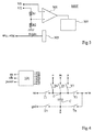
- the figure 1 is an electrical diagram of an example of a multi-cell DC-DC converter.
- the converter comprises two identical or similar elementary cells for conversion DC-DC cell1 and cell2, connected in parallel.
- the converter may comprise more than two elementary cells connected in parallel and / or in series, for example 10 to 100 elementary cells.
- the elementary cells are for example arranged in a matrix according to rows and columns.
- each elementary cell is a charge pump cell adapted to divide the input voltage by a factor of two.
- Each elementary conversion cell comprises a node ve for applying an input voltage, a node vs supplying an output voltage, and a reference node gnd (the input voltage being applied between the node ve and the node gnd, and the output voltage being delivered between the node vs and the node gnd).
- the input nodes ve of all the cells of the converter are connected to the same node VE for applying an input voltage of the converter, the nodes vs of all the cells of the converter are connected to the same supply node VS an output voltage of the converter, and the nodes gnd of all the cells of the converter are connected to the same GND reference node of the converter, for example the ground.
- the input voltage of the converter is applied between the nodes VE and GND, and the output voltage of the converter is delivered between VS and GND nodes.
- An LD load to be powered can be connected between the VS and GND nodes of the converter.
- each elementary conversion cell comprises a first branch comprising two transistors T1 and T2 in series between the nodes ve and vs, a second branch comprising two transistors T3 and T4 in series between the nodes gnd and vs, and capacitor C connecting the midpoint of the series association of transistors T1 and T2 at the midpoint of the series association of transistors T3 and T4.
- the transistors T1 and T4 are P-channel MOS transistors
- the transistors T2 and T3 are N-channel MOS transistors.
- the conduction nodes (source / drain) of the transistor T1 are respectively connected to the node.
- the conduction nodes of the transistor T2 are respectively connected to the first electrode of the capacitor C and to the node vs
- the conduction nodes of the transistor T3 are respectively connected to the node gnd and to the second electrode of the capacitor C
- the conduction nodes of the transistor T4 are respectively connected to the second electrode of the capacitor C and to the node.
- Each elementary conversion cell further comprises an internal control circuit 101 adapted to control the transistors T1, T2, T3 and T4.
- Transistors T1, T2, T3 and T4 are used as switches, i.e., they can be controlled either in the on state or the off state.
- the control gates of the transistors T1 and T4 are connected to the same first output node of the circuit 101, and the control gates of the transistors T2 and T3 are connected to the same second output node of the circuit 101.
- the transistors T1 and T4 on the one hand, and T2 and T3 on the other hand, are therefore simultaneously controlled in the open or closed state.
- the circuit 101 comprises a node in application of a binary signal for activating / deactivating the cell.
- the circuit 101 of the cell maintains the four transistors T1, T2, T3 and T4 of the cell in the open state, so that the cell no longer participates in the supply of the output voltage of the converter.
- the circuit 101 furthermore comprises a clk node for applying a clock signal making it possible to clock the rate of the transfers of the charges from the input to the output of the cell, via the capacitor C.
- the circuit 101 comprises a parameter input of application of a parameterization signal of the cell, on one or more bits, allowing in particular the connection in series and / or in parallel between the different cells.
- the nodes in, clk and param of the control circuits 101 of the different elementary conversion cells are connected to a global control circuit 103 common to all the cells of the matrix.
- each elementary cell of the converter can be controlled by its control circuit 101 alternately in a first state in which the transistors T1 and T4 are on and the transistors T2 and T3 are off, and in a second state in which the transistors T2 and T3 are on and transistors T1 and T4 are off.
- the cell can be periodically controlled alternately in the first state and in the second state, for example with a duty cycle of the order of 0.5, at a frequency fixed by the clock signal applied to the cell's clk node. .
- the average output voltage delivered by the cell is then substantially equal to half the input voltage of the cell.
- the elementary cells of the converter are then controlled substantially in the same way, but with a time shift between the control phases of the different cells respectively in the first state and in the second state.
- An advantage of this control mode is that it limits the oscillations of the output voltage of the converter.
- the described embodiments are however not limited to this particular control mode.
- the clock signals received by the different cells of the converter may be identical and in phase.
- the global control circuit 103 may control the deactivation of certain cells (via their node), for example to limit the consumption of the converter if the power required by the application does not require use all the elementary cells.
- the global control circuit 103 can furthermore control the parameterization of the cells (via their param inputs), for example to modify the ratio between the input voltage and the output voltage, for example by varying the duty cycle between the phases. controlling the cells respectively in the first state and in the second state and / or on the switching frequency and / or on the connections between the different cells.
- a problem that can arise in a multi-cell converter of the type described above is that, in the event of failure of one or more elementary cells, for example if the electrodes of the capacity of an elementary cell enter short. circuit in the example of the figure 1 , malfunctions affecting the entire converter may occur. In particular, the performance of the converter, and in particular its performance, can be reduced considerably. We can also observe a significant increase in the amplitude of oscillations of the output voltage of the converter.
- the dielectric layer separating the two electrodes of the capacitor C in each elementary cell may be relatively thin, for example between 1 and 10 nm thick. Capacities C are then subject to manufacturing dispersions that can lead, in some cases, to a short circuit between the electrodes. A defect of a single elementary cell can then make unusable the entire converter.
- the embodiments described below are applicable to any multi-cell DC-DC converter, integrated or not, with or without capacitors, in which components of the elementary conversion cells (capacitors, inductors, transistors, etc. .) are likely to malfunction.
- a multi-cell DC-DC converter comprising a diagnostic circuit adapted to individually test the elementary conversion cells to detect possible defective cells, to deactivate the defective cells, and to memorize the location of the defective cells.
- the diagnostic circuit is adapted to successively test the different elementary cells at the start of the converter.
- the diagnostic circuit can test the different elementary cells during the operation of the converter, for example during periods of diagnosis repeated periodically.
- the memorization of the locations of the defective cells by the diagnostic circuit makes it possible, at each startup of the converter, to deactivate the cells that have already been identified as defective, without having to test them again.
- the figure 2 is an electrical diagram of an example of an embodiment of a multi-cell DC-DC converter.
- the converter of the figure 2 includes the same elements as the converter of the figure 1 arranged in substantially the same manner. These items will not be detailed again.
- the converter of the figure 2 further comprises a BIST diagnostic circuit connected between the VS and GND terminals of the converter, in parallel with the load LD, and connected to the different elementary conversion cells of the converter.
- the BIST diagnostic circuit is further connected to the input terminal VE of the converter.
- each elementary conversion cell has its activation / deactivation node connected to an output node of the BIST diagnostic circuit.
- the BIST diagnostic circuit is adapted to individually enable / disable the different elementary cells of the converter.
- the BIST diagnostic circuit can individually activate this cell via its activation / deactivation node in, and deactivate all the other cells of the DC-DC converter via their nodes. respectively.
- the diagnosis of the activated cell may, for example, consist of operating the cell and then checking, in steady state, that the ratio between the output voltage VS and the input voltage VE of the DC-DC converter corresponds to the expected ratio. for the cell, within a tolerance range.
- the diagnostic circuit can determine if the output voltage VS of the converter is equal to plus or minus ten percent to r * VE, where r is the theoretical conversion ratio of the tested cell. If so, the cell may be considered healthy, and if not, the cell may be considered defective.
- the BIST diagnostic circuit may implement a conversion efficiency measurement, and / or a measurement of oscillations of the output voltage of the converter, and determine whether the measured values are in accordance with the expected operation of the cell.
- the elementary cells of the converter may be tested sequentially, the state of each cell being tested being stored in a memory of the BIST diagnostic circuit, preferably a nonvolatile memory so as to retain the health status information of the cells when the DC-DC converter stops being powered.
- the diagnosis of the converter can be achieved by dichotomic search for any defective elementary cells.
- all the elementary cells of the converter may initially be activated by the diagnostic circuit. The diagnostic circuit then determines whether the converter behaves in the expected manner. If so, the diagnostic circuit may consider all activated elementary cells to be healthy, and interrupt the diagnosis. If not, the diagnostic circuit can disable half of the cells, and repeat the test. If the behavior of the activated cells is in accordance with the expected behavior, the diagnostic circuit may consider that the activated cells are healthy, and that the defective cell (s) are in the other half of the converter. By dichotomic search, the diagnostic circuit can thus identify the defective cell (s) without having to individually test each of the cells.
- the performance of the DC-DC converter may be slightly reduced compared to a converter in which all cells are healthy and active.
- the performances obtained remain very much higher than the performances obtained when cells are defective and are not deactivated.
- the inventors have carried out measurements for a DC-DC converter comprising 30 elementary cells of the type represented in FIGS. Figures 1 and 2 and having, when all the cells are healthy and activated, a yield of 78% and an output oscillation rate of 0.3%.
- faulting (short circuit) of a single elementary cell of the converter causes a drop to 67% of the conversion efficiency, and an increase to 2.2% of the output oscillation rate.
- the defect of two elementary cells leads to a drop to 59% of the conversion efficiency, and a 4.3% increase in the output oscillation rate.
- the diagnostic circuit of the figure 2 to disable the defective cells, there is only a slight decrease at 77% of the yield and a slight increase to 0.9% of the output oscillation rate when one or two cells are defective.
- the proposed embodiment makes it possible to continue to use, without significant performance degradation, multi-cell DC-DC converters with defective cells.
- This embodiment is particularly advantageous in the case of a converter integrated in and on a semiconductor chip, in which the repair or replacement of a defective elementary cell is not possible.
- the diagnostic circuit BIST is for example integrated on the same semiconductor chip as the elementary cells and the control circuit 103 of the converter.
- the overall control circuit 103 can reconfigure the way that these phase shifts are substantially uniformly distributed, that is to say so that the NN def clock signals received by the NN def still active cells ( N being the total number of cells of the converter and N def being the number of defective cells deactivated) are out of phase two by two of approximately T clk / (NN def ), T clk being the period of the clock signal.
- N being the total number of cells of the converter and N def being the number of defective cells deactivated
- T clk being the period of the clock signal.
- the diagnostic circuit BIST can disconnect the load LD intended to be fed by the converter, the cells being then tested empty. Alternatively, the cells can be tested by keeping the load LD connected to the output of the converter. Alternatively, the diagnostic circuit BIST may include a diagnostic load (not shown), for example a diagnostic resistor, connected between the terminals VS and GND only during the diagnostic phases (the load LD can then be disconnected or kept connected).
- a diagnostic load (not shown), for example a diagnostic resistor, connected between the terminals VS and GND only during the diagnostic phases (the load LD can then be disconnected or kept connected). The provision of such a diagnostic load makes it easier to discriminate between defective cells and healthy cells, especially when the characteristics of the LD load are not known with certainty.
- the figure 3 is a circuit diagram of an exemplary embodiment of the diagnostic circuit BIST of the converter of the figure 2 .
- the BIST circuit comprises a comparator 301, a first input (+) of which is connected to the terminal VS, and a second input (-) of which is connected to the midpoint of a voltage divider bridge comprising two resistors.
- R1 and R2 in series between the VE terminal and the GND terminal.
- Resistors R1 and R2 are chosen so that the voltage applied to the second input (-) of the comparator 301 is equal to r * (1-m) * VE, where r is the expected conversion ratio of an elementary conversion cell, and m is a margin of tolerance, for example of the order of 10%.
- the output of the comparator is in a first state, meaning that the cell tested is healthy, and if the voltage VS is lower than the voltage r * (1-m) * VE, the comparator is in a second state, meaning that the cell being tested is defective.
- the output of the comparator 301 is connected to a storage circuit 303 comprising for example a memory location per elementary cell of the converter.
- the circuit 303 is adapted to record, for each cell tested, the result of the test in the memory location associated with the cell.
- the BIST circuit further comprises a selection circuit 305 for individually activating the different elementary conversion cells in order to test their output voltage.
- the comparator 301 can advantageously be used outside the diagnostic phases, to perform other functions, for example to implement a regulation function of the converter, comprising the servo-control of one or more converter parameters on the voltage measured at the output of the converter.
- the figure 4 is a circuit diagram of another example of an elementary cell for converting a multi-cell DC-DC converter according to one embodiment.
- the elementary cell of the figure 4 includes, as in the examples of Figures 1 and 2 , an application node of an input voltage, a node vs supply of an output voltage, a reference node gnd, a first branch comprising two switches T1 and T2 in series between the nodes ve and vs , a second branch having two switches T3 and T4 in series between the nodes gnd and vs, and a capacitor C connecting a common node 1 between the switches T1 and T2 at a common node n between the switches T3 and T4.
- the elementary cell further comprises a switch T5 connecting the node 1 to a connection node m of the cell, a switch T6 connecting the node 1 to a connection node o of the cell, and a switch T7 connecting the node 1 to a connection node p of the cell.
- the switches T5, T6, T7 are, for example, MOS transistors.
- the elementary cell of conversion of the figure 4 further comprises an internal control circuit 101 adapted to control the switches T1, T2, T3, T4, T5, T6 and T7 of the cell.
- the circuit 101 comprises a node in application of a binary signal for activating / deactivating the cell. For example, when the cell is controlled in the deactivated state via its node at, the circuit 101 of the cell holds the seven switches T1, T2, T3, T4, T5, T6, T7 from the cell to the cell. open state, so that the cell no longer participates in supplying the output voltage of the converter.
- the circuit 101 further comprises a clk node for applying a clock signal for timing the control of the switches T1, T2, T3, T4, T5, T6 and T7 of the cell.
- the circuit 101 comprises a parameter input for applying a parameterisation signal of the cell, on one or more bits, making it possible to define the control sequence of the switches T1, T2, T3, T4, T5, T6, T7 of the cell, in particular to set the connection mode in series and / or in parallel between the different elementary cells of the converter, and, if necessary, the mode of operation of the converter.
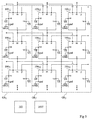
- the figure 5 is a simplified electrical diagram of an example of an embodiment of a multi-cell DC-DC converter.
- the converter of the figure 5 comprises a plurality of elementary conversion cells 100 ij identical or similar to the cell of the figure 4 .
- the cells 100 ij are arranged in a matrix according to lines and columns, the indices i and j respectively denoting the rank of the row and the rank of the column to which a cell belongs, with i integer ranging from 1 to M and j integer ranging from 1 to N, M and N being integers respectively denoting the number of rows and the number of columns of the matrix of elementary cells.
- the elementary cells 100 ij are not detailed on the figure 5 . Only the connection nodes ve, vs, gnd, m, n, o and p of the cells 100 ij are represented. In the example of the figure 5 , the elementary cells of the converter are all connected in parallel via their nodes ve, vs and gnd.
- the input nodes ve of all the cells of the converter are connected to the same node VE of application of an input voltage of the converter, the nodes vs of all the cells of the converter are connected to the same node VS for supplying an output voltage of the converter, and the nodes gnd of all the cells of the converter are connected to the same reference node GND of the converter, for example the ground.
- the input voltage of the converter is applied between the nodes VE and GND, and the output voltage of the converter is delivered between the nodes VS and GND.
- a load to feed (not shown on the figure 5 ) can be connected between the VS and GND nodes of the converter.
- each elementary cell 100 ij (with the exception of the cells of the first row of the matrix) has its node m connected to the node n of the cell 100 i-1j .
- each elementary cell 100 ij (with the exception of the cells of the first column of the matrix) has its node o connected to the node m of the cell 100 ij-1 .
- each elementary cell 100 ij (with the exception of the cells of the last column of the matrix) has its node p connected to the node m of the cell 100 ij + 1.
- control circuits 101 of the different elementary conversion cells are connected to the same overall control circuit 103 common to all the cells of the matrix.
- the different cells of the converter receive for example the same clock signal, with or without phase shift between the different cells of the converter.
- the global control circuit 103 may control the deactivation of certain cells (via their node), for example to limit the consumption of the converter if the power required by the application does not require use all the elementary cells.
- the global control circuit 103 can furthermore control the parameterization of the cells (via their param inputs) as a function of the desired operating mode of the converter, for example to modify the ratio between the input voltage and the output voltage of the converter. playing on the modes of interconnection between the different cells.
- the switches T5, T6 and T7 of the elementary cells are kept open, and each active elementary cell of the converter is controlled by its control circuit 101 alternately in a first state in which the switches T1 and T4 are closed. and the switches T2 and T3 are open, and in a second state in which the switches T1 and T4 are open and the switches T2 and T3 are closed.
- Each cell is for example periodically controlled alternately in the first state and in the second state, for example with a duty cycle of the order of 0.5, at a frequency set by the clock signal applied to the node clk of the cell.
- the behavior of the converter is then similar to that of converters Figures 1 and 2 . In steady state, the average output voltage delivered by the converter is substantially equal to half the input voltage of the converter.
- the active elementary cells of the converter are connected in groups of at least two neighboring elementary cells via their switches T5, T6 and / or T7, so that to define a different conversion ratio of 0.5 between the output voltage and the input voltage of the converter.
- each group GR j is controlled, by means of the control circuits 101 of the elementary cells 100 ij of the group, alternately in a first state in which the capacitors C of the cells of the group are connected in series between the nodes VE and VS of the converter, and in a second state in which the capacitances C of the cells of the group are connected in parallel between the nodes VS and GND of the converter.
- Each group GR i is for example periodically controlled alternately in the first state and in the second state, for example with a duty cycle of the order of 0.5, at a frequency set by the clock signal applied to the clk nodes. cells of the group. In steady state, the average output voltage delivered by the converter is then substantially equal to one quarter of the input voltage of the converter.
- the parameterization of the operating mode of the converter can be achieved by the global control circuit 103 which generates, for each active elementary cell 100 ij of the converter, a parameterization signal applied to the param input of the cell.
- the parameterization signal comprises, for example, one or more bits setting the desired conversion ratio, and, where appropriate, the position of the cell in a group of neighboring cells co-operating to implement a function of determined conversion.
- the internal control circuit 101 of each elementary cell applies a control sequence appropriate to the switches T1, T2, T3, T4, T5, T6, T7 of the cell.
- the converter of the figure 5 further comprises a BIST diagnostic circuit adapted to individually test the elementary conversion cells 100 ij to detect any defective cells.
- the BIST diagnostic circuit of the figure 5 is for example identical or similar, in its arrangement and in its operation, to the diagnostic circuit BIST of the figure 2 .
- the BIST circuit is adapted, at the end of a diagnostic phase, to deactivate the defective cells and to memorize their location.
- the global control circuit 103 may, at the end of the diagnostic phase, modify the parameterization of the remaining active cells so as to modify the sequence controlling switches of these cells.
- the different elementary conversion cells receive phase-shifted clock signals
- the elementary cells are connected in elementary groups of several neighboring cells to implement a particular conversion function, as per example in the second mode of operation described above in relation to the figure 5
- the diagnostic circuit BIST when elementary cells are diagnosed defective in several elementary groups and are deactivated by the diagnostic circuit BIST, it is possible to modify the parameterization of the remaining active cells, so as to recreate, where possible, one or more elementary groups. from the healthy cells remaining from the defective groups.
- the cells 100 21 and 100 12 are diagnosed as defective, rather than deactivating all of the two elementary groups GR 1 and GR 2 of the converter, it is possible to reconfigure the cells 100 11 , 100 22 and 100 31 into a new one.
- the global control circuit 103 may comprise a memory storing configuration tables making it possible to identify, for each mode of operation of the converter and for each elementary cell of the converter, the neighboring elementary cell or cells can be combined with the cell in question to form an elementary group adapted to implement the desired conversion function.
- the global control circuit 103 may comprise logic circuits adapted to implement a search algorithm for neighboring healthy cells capable of being combined into a new elementary group adapted to implement the desired conversion function.
- the embodiments described are not limited to the example of a diagnostic circuit described in connection with the figure 3 .
- Those skilled in the art will be able to provide other implementations of the BIST diagnostic circuit making it possible to implement the desired operation.
- the embodiments described are not limited to the particular examples of elementary conversion cells illustrated by the Figures 1, 2 and 4 . More generally, the described embodiments apply to any type of elementary DC-DC conversion cell comprising at least one switch and a passive energy storage element, for example a capacitance or an inductance.
- the elementary cells may be capacitive charge pump cells performing division or multiplication of the input voltage.
- the elementary conversion cells may be inductive conversion cells.
- the embodiments described are not limited to the particular case where the switches of the elementary conversion cells are MOS transistors.
Landscapes
- Engineering & Computer Science (AREA)
- Power Engineering (AREA)
- Dc-Dc Converters (AREA)
Applications Claiming Priority (1)
| Application Number | Priority Date | Filing Date | Title |
|---|---|---|---|
| FR1552451 | 2015-03-24 |
Publications (3)
| Publication Number | Publication Date |
|---|---|
| EP3076535A2 true EP3076535A2 (de) | 2016-10-05 |
| EP3076535A3 EP3076535A3 (de) | 2016-12-28 |
| EP3076535B1 EP3076535B1 (de) | 2018-06-27 |
Family
ID=53541739
Family Applications (1)
| Application Number | Title | Priority Date | Filing Date |
|---|---|---|---|
| EP16161749.3A Active EP3076535B1 (de) | 2015-03-24 | 2016-03-22 | Gleichstrom-gleichstromwandler |
Country Status (2)
| Country | Link |
|---|---|
| US (1) | US9929642B2 (de) |
| EP (1) | EP3076535B1 (de) |
Cited By (1)
| Publication number | Priority date | Publication date | Assignee | Title |
|---|---|---|---|---|
| EP3667898A1 (de) * | 2018-12-14 | 2020-06-17 | Schneider Toshiba Inverter Europe SAS | Steuerung einer anzahl von aktiven leistungszellen eines drehzahlreglers |
Families Citing this family (2)
| Publication number | Priority date | Publication date | Assignee | Title |
|---|---|---|---|---|
| CN105811794B (zh) * | 2016-05-06 | 2018-03-30 | 上海海事大学 | 多电平逆变器的参考电压信号重构的容错控制方法 |
| EP4586481A1 (de) * | 2024-01-10 | 2025-07-16 | Murata Manufacturing Co., Ltd. | Redundante hochspannungserzeugung auf einem chip |
Family Cites Families (7)
| Publication number | Priority date | Publication date | Assignee | Title |
|---|---|---|---|---|
| FR2835116B1 (fr) * | 2002-01-22 | 2005-07-08 | Johnson Contr Automotive Elect | Convertisseur de tension dc/dc multi-cellules |
| ITMI20021902A1 (it) * | 2002-09-06 | 2004-03-07 | Atmel Corp | Architettura di pompa di carica modulare |
| US6859091B1 (en) * | 2003-09-18 | 2005-02-22 | Maxim Integrated Products, Inc. | Continuous linear regulated zero dropout charge pump with high efficiency load predictive clocking scheme |
| US20080054990A1 (en) * | 2006-08-30 | 2008-03-06 | Taiwan Semiconductor Manufacturing Co., Ltd. | Charge pump method and architecture |
| US8120975B2 (en) * | 2009-01-29 | 2012-02-21 | Freescale Semiconductor, Inc. | Memory having negative voltage write assist circuit and method therefor |
| WO2013147727A1 (en) * | 2012-03-25 | 2013-10-03 | Intel Corporation | Charge pump redundancy in a memory |
| US8976554B2 (en) | 2012-09-18 | 2015-03-10 | Siemens Corporation | Control for fault-bypass of cascaded multi-level inverter |
-
2016
- 2016-03-22 EP EP16161749.3A patent/EP3076535B1/de active Active
- 2016-03-22 US US15/077,380 patent/US9929642B2/en active Active
Non-Patent Citations (1)
| Title |
|---|
| None |
Cited By (4)
| Publication number | Priority date | Publication date | Assignee | Title |
|---|---|---|---|---|
| EP3667898A1 (de) * | 2018-12-14 | 2020-06-17 | Schneider Toshiba Inverter Europe SAS | Steuerung einer anzahl von aktiven leistungszellen eines drehzahlreglers |
| FR3090244A1 (fr) * | 2018-12-14 | 2020-06-19 | Schneider Toshiba Inverter Europe Sas | Gestion de nombre de cellules de puissance actives d’un variateur de vitesse |
| RU2757695C2 (ru) * | 2018-12-14 | 2021-10-20 | Шнейдер Тосиба Инвертер Юроп Сас | Управление числом активных силовых элементов регулятора скорости |
| US11509252B2 (en) | 2018-12-14 | 2022-11-22 | Schneider Toshiba Inverter Europe Sas | Management of the number of active power cells of a variable speed drive |
Also Published As
| Publication number | Publication date |
|---|---|
| US20160285362A1 (en) | 2016-09-29 |
| EP3076535B1 (de) | 2018-06-27 |
| US9929642B2 (en) | 2018-03-27 |
| EP3076535A3 (de) | 2016-12-28 |
Similar Documents
| Publication | Publication Date | Title |
|---|---|---|
| EP2944008B1 (de) | Ladungsausgleich innerhalb einer elektrischen batterie | |
| CA2789460A1 (fr) | Systeme d'equilibrage par couplage magnetique d'une association serie d'elements de generation ou de stockage d'energie electrique | |
| EP3076535B1 (de) | Gleichstrom-gleichstromwandler | |
| CA3102416A1 (fr) | Systeme electrique a cellules commutees et procede de commande d'un tel systeme | |
| WO2005031942A1 (fr) | Systeme d'equilibrage d'un dispositif de stockage d'energie | |
| FR3005815B1 (fr) | Systeme de generation d'un signal analogique | |
| EP3579233A1 (de) | Elementarzelle und ladepumpen, die eine solche elementarzelle umfassen | |
| EP3032729B1 (de) | Gleichstrom-gleichstrom-wandler mit kaltstart | |
| FR3040113A1 (fr) | Convertisseur dc-dc | |
| EP3654534B1 (de) | Kapazitive logische zelle | |
| CA3085328A1 (fr) | Batterie a accumulateurs commutes | |
| EP1961115B1 (de) | Elektronische schaltung mit kompensation des intrinsischen offsets von differenzpaaren | |
| EP3724962B1 (de) | Batterie mit geschalteten akkumulatoren | |
| FR2860353A1 (fr) | Module de transfert de charges entre deux dipoles | |
| FR2996005A1 (fr) | Procede de conception d'un circuit electronique | |
| FR2719148A1 (fr) | Circuit multiplicateur de tension. | |
| EP3735729B1 (de) | Batterie mit geschalteten akkumulatoren | |
| US20240222820A1 (en) | Voltage measurement device and cell stack system | |
| FR3039006A1 (fr) | Dispositif de gestion d'un assemblage de cellules de stockage ou de production d'energie electrique | |
| FR3082315A1 (fr) | Procede de detection d'un dysfonctionnement d'un circuit limiteur de tension et systeme de controle pour la mise en œuvre dudit procede de detection de dysfonctionnement | |
| FR3096548A1 (fr) | Correction d'une valeur d'un composant passif | |
| EP4639771A1 (de) | Genauer synchroner analogzähler | |
| WO2003030343A2 (fr) | Generateur de haute tension incorpore dans un circuit integre | |
| EP3156812A1 (de) | Elektronisches steuersystem einer elektrischen batterie |
Legal Events
| Date | Code | Title | Description |
|---|---|---|---|
| PUAI | Public reference made under article 153(3) epc to a published international application that has entered the european phase |
Free format text: ORIGINAL CODE: 0009012 |
|
| AK | Designated contracting states |
Kind code of ref document: A2 Designated state(s): AL AT BE BG CH CY CZ DE DK EE ES FI FR GB GR HR HU IE IS IT LI LT LU LV MC MK MT NL NO PL PT RO RS SE SI SK SM TR |
|
| AX | Request for extension of the european patent |
Extension state: BA ME |
|
| PUAL | Search report despatched |
Free format text: ORIGINAL CODE: 0009013 |
|
| AK | Designated contracting states |
Kind code of ref document: A3 Designated state(s): AL AT BE BG CH CY CZ DE DK EE ES FI FR GB GR HR HU IE IS IT LI LT LU LV MC MK MT NL NO PL PT RO RS SE SI SK SM TR |
|
| AX | Request for extension of the european patent |
Extension state: BA ME |
|
| RIC1 | Information provided on ipc code assigned before grant |
Ipc: G11C 5/14 20060101ALI20161122BHEP Ipc: H02M 1/32 20070101AFI20161122BHEP Ipc: H02M 3/07 20060101ALI20161122BHEP Ipc: H02M 7/483 20070101ALI20161122BHEP |
|
| STAA | Information on the status of an ep patent application or granted ep patent |
Free format text: STATUS: REQUEST FOR EXAMINATION WAS MADE |
|
| 17P | Request for examination filed |
Effective date: 20170412 |
|
| RBV | Designated contracting states (corrected) |
Designated state(s): AL AT BE BG CH CY CZ DE DK EE ES FI FR GB GR HR HU IE IS IT LI LT LU LV MC MK MT NL NO PL PT RO RS SE SI SK SM TR |
|
| RIC1 | Information provided on ipc code assigned before grant |
Ipc: G11C 5/14 20060101ALI20180129BHEP Ipc: H02M 7/483 20070101ALI20180129BHEP Ipc: H02M 1/32 20070101AFI20180129BHEP Ipc: H02M 3/07 20060101ALI20180129BHEP |
|
| GRAP | Despatch of communication of intention to grant a patent |
Free format text: ORIGINAL CODE: EPIDOSNIGR1 |
|
| STAA | Information on the status of an ep patent application or granted ep patent |
Free format text: STATUS: GRANT OF PATENT IS INTENDED |
|
| INTG | Intention to grant announced |
Effective date: 20180314 |
|
| GRAS | Grant fee paid |
Free format text: ORIGINAL CODE: EPIDOSNIGR3 |
|
| GRAA | (expected) grant |
Free format text: ORIGINAL CODE: 0009210 |
|
| STAA | Information on the status of an ep patent application or granted ep patent |
Free format text: STATUS: THE PATENT HAS BEEN GRANTED |
|
| AK | Designated contracting states |
Kind code of ref document: B1 Designated state(s): AL AT BE BG CH CY CZ DE DK EE ES FI FR GB GR HR HU IE IS IT LI LT LU LV MC MK MT NL NO PL PT RO RS SE SI SK SM TR |
|
| REG | Reference to a national code |
Ref country code: GB Ref legal event code: FG4D Free format text: NOT ENGLISH |
|
| REG | Reference to a national code |
Ref country code: AT Ref legal event code: REF Ref document number: 1013178 Country of ref document: AT Kind code of ref document: T Effective date: 20180715 |
|
| REG | Reference to a national code |
Ref country code: IE Ref legal event code: FG4D Free format text: LANGUAGE OF EP DOCUMENT: FRENCH |
|
| REG | Reference to a national code |
Ref country code: DE Ref legal event code: R096 Ref document number: 602016003760 Country of ref document: DE |
|
| PG25 | Lapsed in a contracting state [announced via postgrant information from national office to epo] |
Ref country code: BG Free format text: LAPSE BECAUSE OF FAILURE TO SUBMIT A TRANSLATION OF THE DESCRIPTION OR TO PAY THE FEE WITHIN THE PRESCRIBED TIME-LIMIT Effective date: 20180927 Ref country code: NO Free format text: LAPSE BECAUSE OF FAILURE TO SUBMIT A TRANSLATION OF THE DESCRIPTION OR TO PAY THE FEE WITHIN THE PRESCRIBED TIME-LIMIT Effective date: 20180927 Ref country code: FI Free format text: LAPSE BECAUSE OF FAILURE TO SUBMIT A TRANSLATION OF THE DESCRIPTION OR TO PAY THE FEE WITHIN THE PRESCRIBED TIME-LIMIT Effective date: 20180627 Ref country code: SE Free format text: LAPSE BECAUSE OF FAILURE TO SUBMIT A TRANSLATION OF THE DESCRIPTION OR TO PAY THE FEE WITHIN THE PRESCRIBED TIME-LIMIT Effective date: 20180627 Ref country code: LT Free format text: LAPSE BECAUSE OF FAILURE TO SUBMIT A TRANSLATION OF THE DESCRIPTION OR TO PAY THE FEE WITHIN THE PRESCRIBED TIME-LIMIT Effective date: 20180627 |
|
| REG | Reference to a national code |
Ref country code: NL Ref legal event code: MP Effective date: 20180627 |
|
| REG | Reference to a national code |
Ref country code: LT Ref legal event code: MG4D |
|
| PG25 | Lapsed in a contracting state [announced via postgrant information from national office to epo] |
Ref country code: RS Free format text: LAPSE BECAUSE OF FAILURE TO SUBMIT A TRANSLATION OF THE DESCRIPTION OR TO PAY THE FEE WITHIN THE PRESCRIBED TIME-LIMIT Effective date: 20180627 Ref country code: LV Free format text: LAPSE BECAUSE OF FAILURE TO SUBMIT A TRANSLATION OF THE DESCRIPTION OR TO PAY THE FEE WITHIN THE PRESCRIBED TIME-LIMIT Effective date: 20180627 Ref country code: HR Free format text: LAPSE BECAUSE OF FAILURE TO SUBMIT A TRANSLATION OF THE DESCRIPTION OR TO PAY THE FEE WITHIN THE PRESCRIBED TIME-LIMIT Effective date: 20180627 Ref country code: GR Free format text: LAPSE BECAUSE OF FAILURE TO SUBMIT A TRANSLATION OF THE DESCRIPTION OR TO PAY THE FEE WITHIN THE PRESCRIBED TIME-LIMIT Effective date: 20180928 |
|
| REG | Reference to a national code |
Ref country code: AT Ref legal event code: MK05 Ref document number: 1013178 Country of ref document: AT Kind code of ref document: T Effective date: 20180627 |
|
| PG25 | Lapsed in a contracting state [announced via postgrant information from national office to epo] |
Ref country code: NL Free format text: LAPSE BECAUSE OF FAILURE TO SUBMIT A TRANSLATION OF THE DESCRIPTION OR TO PAY THE FEE WITHIN THE PRESCRIBED TIME-LIMIT Effective date: 20180627 |
|
| PG25 | Lapsed in a contracting state [announced via postgrant information from national office to epo] |
Ref country code: AT Free format text: LAPSE BECAUSE OF FAILURE TO SUBMIT A TRANSLATION OF THE DESCRIPTION OR TO PAY THE FEE WITHIN THE PRESCRIBED TIME-LIMIT Effective date: 20180627 Ref country code: CZ Free format text: LAPSE BECAUSE OF FAILURE TO SUBMIT A TRANSLATION OF THE DESCRIPTION OR TO PAY THE FEE WITHIN THE PRESCRIBED TIME-LIMIT Effective date: 20180627 Ref country code: IS Free format text: LAPSE BECAUSE OF FAILURE TO SUBMIT A TRANSLATION OF THE DESCRIPTION OR TO PAY THE FEE WITHIN THE PRESCRIBED TIME-LIMIT Effective date: 20181027 Ref country code: RO Free format text: LAPSE BECAUSE OF FAILURE TO SUBMIT A TRANSLATION OF THE DESCRIPTION OR TO PAY THE FEE WITHIN THE PRESCRIBED TIME-LIMIT Effective date: 20180627 Ref country code: EE Free format text: LAPSE BECAUSE OF FAILURE TO SUBMIT A TRANSLATION OF THE DESCRIPTION OR TO PAY THE FEE WITHIN THE PRESCRIBED TIME-LIMIT Effective date: 20180627 Ref country code: PL Free format text: LAPSE BECAUSE OF FAILURE TO SUBMIT A TRANSLATION OF THE DESCRIPTION OR TO PAY THE FEE WITHIN THE PRESCRIBED TIME-LIMIT Effective date: 20180627 Ref country code: SK Free format text: LAPSE BECAUSE OF FAILURE TO SUBMIT A TRANSLATION OF THE DESCRIPTION OR TO PAY THE FEE WITHIN THE PRESCRIBED TIME-LIMIT Effective date: 20180627 |
|
| PG25 | Lapsed in a contracting state [announced via postgrant information from national office to epo] |
Ref country code: SM Free format text: LAPSE BECAUSE OF FAILURE TO SUBMIT A TRANSLATION OF THE DESCRIPTION OR TO PAY THE FEE WITHIN THE PRESCRIBED TIME-LIMIT Effective date: 20180627 Ref country code: IT Free format text: LAPSE BECAUSE OF FAILURE TO SUBMIT A TRANSLATION OF THE DESCRIPTION OR TO PAY THE FEE WITHIN THE PRESCRIBED TIME-LIMIT Effective date: 20180627 Ref country code: ES Free format text: LAPSE BECAUSE OF FAILURE TO SUBMIT A TRANSLATION OF THE DESCRIPTION OR TO PAY THE FEE WITHIN THE PRESCRIBED TIME-LIMIT Effective date: 20180627 |
|
| REG | Reference to a national code |
Ref country code: DE Ref legal event code: R097 Ref document number: 602016003760 Country of ref document: DE |
|
| PLBE | No opposition filed within time limit |
Free format text: ORIGINAL CODE: 0009261 |
|
| STAA | Information on the status of an ep patent application or granted ep patent |
Free format text: STATUS: NO OPPOSITION FILED WITHIN TIME LIMIT |
|
| PG25 | Lapsed in a contracting state [announced via postgrant information from national office to epo] |
Ref country code: DK Free format text: LAPSE BECAUSE OF FAILURE TO SUBMIT A TRANSLATION OF THE DESCRIPTION OR TO PAY THE FEE WITHIN THE PRESCRIBED TIME-LIMIT Effective date: 20180627 |
|
| 26N | No opposition filed |
Effective date: 20190328 |
|
| PG25 | Lapsed in a contracting state [announced via postgrant information from national office to epo] |
Ref country code: SI Free format text: LAPSE BECAUSE OF FAILURE TO SUBMIT A TRANSLATION OF THE DESCRIPTION OR TO PAY THE FEE WITHIN THE PRESCRIBED TIME-LIMIT Effective date: 20180627 |
|
| PG25 | Lapsed in a contracting state [announced via postgrant information from national office to epo] |
Ref country code: MC Free format text: LAPSE BECAUSE OF FAILURE TO SUBMIT A TRANSLATION OF THE DESCRIPTION OR TO PAY THE FEE WITHIN THE PRESCRIBED TIME-LIMIT Effective date: 20180627 |
|
| REG | Reference to a national code |
Ref country code: CH Ref legal event code: PL |
|
| PG25 | Lapsed in a contracting state [announced via postgrant information from national office to epo] |
Ref country code: AL Free format text: LAPSE BECAUSE OF FAILURE TO SUBMIT A TRANSLATION OF THE DESCRIPTION OR TO PAY THE FEE WITHIN THE PRESCRIBED TIME-LIMIT Effective date: 20180627 Ref country code: LU Free format text: LAPSE BECAUSE OF NON-PAYMENT OF DUE FEES Effective date: 20190322 |
|
| REG | Reference to a national code |
Ref country code: BE Ref legal event code: MM Effective date: 20190331 |
|
| PG25 | Lapsed in a contracting state [announced via postgrant information from national office to epo] |
Ref country code: IE Free format text: LAPSE BECAUSE OF NON-PAYMENT OF DUE FEES Effective date: 20190322 Ref country code: LI Free format text: LAPSE BECAUSE OF NON-PAYMENT OF DUE FEES Effective date: 20190331 Ref country code: CH Free format text: LAPSE BECAUSE OF NON-PAYMENT OF DUE FEES Effective date: 20190331 |
|
| PG25 | Lapsed in a contracting state [announced via postgrant information from national office to epo] |
Ref country code: BE Free format text: LAPSE BECAUSE OF NON-PAYMENT OF DUE FEES Effective date: 20190331 |
|
| PG25 | Lapsed in a contracting state [announced via postgrant information from national office to epo] |
Ref country code: TR Free format text: LAPSE BECAUSE OF FAILURE TO SUBMIT A TRANSLATION OF THE DESCRIPTION OR TO PAY THE FEE WITHIN THE PRESCRIBED TIME-LIMIT Effective date: 20180627 |
|
| PG25 | Lapsed in a contracting state [announced via postgrant information from national office to epo] |
Ref country code: PT Free format text: LAPSE BECAUSE OF FAILURE TO SUBMIT A TRANSLATION OF THE DESCRIPTION OR TO PAY THE FEE WITHIN THE PRESCRIBED TIME-LIMIT Effective date: 20181029 Ref country code: MT Free format text: LAPSE BECAUSE OF FAILURE TO SUBMIT A TRANSLATION OF THE DESCRIPTION OR TO PAY THE FEE WITHIN THE PRESCRIBED TIME-LIMIT Effective date: 20180627 |
|
| GBPC | Gb: european patent ceased through non-payment of renewal fee |
Effective date: 20200322 |
|
| PG25 | Lapsed in a contracting state [announced via postgrant information from national office to epo] |
Ref country code: GB Free format text: LAPSE BECAUSE OF NON-PAYMENT OF DUE FEES Effective date: 20200322 |
|
| PG25 | Lapsed in a contracting state [announced via postgrant information from national office to epo] |
Ref country code: CY Free format text: LAPSE BECAUSE OF FAILURE TO SUBMIT A TRANSLATION OF THE DESCRIPTION OR TO PAY THE FEE WITHIN THE PRESCRIBED TIME-LIMIT Effective date: 20180627 |
|
| PG25 | Lapsed in a contracting state [announced via postgrant information from national office to epo] |
Ref country code: HU Free format text: LAPSE BECAUSE OF FAILURE TO SUBMIT A TRANSLATION OF THE DESCRIPTION OR TO PAY THE FEE WITHIN THE PRESCRIBED TIME-LIMIT; INVALID AB INITIO Effective date: 20160322 |
|
| PG25 | Lapsed in a contracting state [announced via postgrant information from national office to epo] |
Ref country code: MK Free format text: LAPSE BECAUSE OF FAILURE TO SUBMIT A TRANSLATION OF THE DESCRIPTION OR TO PAY THE FEE WITHIN THE PRESCRIBED TIME-LIMIT Effective date: 20180627 |
|
| PGFP | Annual fee paid to national office [announced via postgrant information from national office to epo] |
Ref country code: DE Payment date: 20250319 Year of fee payment: 10 |
|
| PGFP | Annual fee paid to national office [announced via postgrant information from national office to epo] |
Ref country code: FR Payment date: 20250318 Year of fee payment: 10 |