EP3076435A1 - Semiconductor device - Google Patents
Semiconductor device Download PDFInfo
- Publication number
- EP3076435A1 EP3076435A1 EP14862551.0A EP14862551A EP3076435A1 EP 3076435 A1 EP3076435 A1 EP 3076435A1 EP 14862551 A EP14862551 A EP 14862551A EP 3076435 A1 EP3076435 A1 EP 3076435A1
- Authority
- EP
- European Patent Office
- Prior art keywords
- region
- drain
- conductive
- trench isolation
- isolation structure
- Prior art date
- Legal status (The legal status is an assumption and is not a legal conclusion. Google has not performed a legal analysis and makes no representation as to the accuracy of the status listed.)
- Granted
Links
Images



Classifications
-
- H—ELECTRICITY
- H10—SEMICONDUCTOR DEVICES; ELECTRIC SOLID-STATE DEVICES NOT OTHERWISE PROVIDED FOR
- H10D—INORGANIC ELECTRIC SEMICONDUCTOR DEVICES
- H10D30/00—Field-effect transistors [FET]
- H10D30/60—Insulated-gate field-effect transistors [IGFET]
- H10D30/64—Double-diffused metal-oxide semiconductor [DMOS] FETs
- H10D30/65—Lateral DMOS [LDMOS] FETs
- H10D30/659—Lateral DMOS [LDMOS] FETs having voltage-sensing or current-sensing structures, e.g. emulator sections or overcurrent sensing cells
-
- H—ELECTRICITY
- H10—SEMICONDUCTOR DEVICES; ELECTRIC SOLID-STATE DEVICES NOT OTHERWISE PROVIDED FOR
- H10D—INORGANIC ELECTRIC SEMICONDUCTOR DEVICES
- H10D86/00—Integrated devices formed in or on insulating or conducting substrates, e.g. formed in silicon-on-insulator [SOI] substrates or on stainless steel or glass substrates
- H10D86/201—Integrated devices formed in or on insulating or conducting substrates, e.g. formed in silicon-on-insulator [SOI] substrates or on stainless steel or glass substrates the substrates comprising an insulating layer on a semiconductor body, e.g. SOI
-
- H—ELECTRICITY
- H10—SEMICONDUCTOR DEVICES; ELECTRIC SOLID-STATE DEVICES NOT OTHERWISE PROVIDED FOR
- H10D—INORGANIC ELECTRIC SEMICONDUCTOR DEVICES
- H10D30/00—Field-effect transistors [FET]
- H10D30/60—Insulated-gate field-effect transistors [IGFET]
- H10D30/601—Insulated-gate field-effect transistors [IGFET] having lightly-doped drain or source extensions, e.g. LDD IGFETs or DDD IGFETs
- H10D30/603—Insulated-gate field-effect transistors [IGFET] having lightly-doped drain or source extensions, e.g. LDD IGFETs or DDD IGFETs having asymmetry in the channel direction, e.g. lateral high-voltage MISFETs having drain offset region or extended drain IGFETs [EDMOS]
-
- H—ELECTRICITY
- H10—SEMICONDUCTOR DEVICES; ELECTRIC SOLID-STATE DEVICES NOT OTHERWISE PROVIDED FOR
- H10D—INORGANIC ELECTRIC SEMICONDUCTOR DEVICES
- H10D30/00—Field-effect transistors [FET]
- H10D30/60—Insulated-gate field-effect transistors [IGFET]
- H10D30/64—Double-diffused metal-oxide semiconductor [DMOS] FETs
- H10D30/65—Lateral DMOS [LDMOS] FETs
- H10D30/657—Lateral DMOS [LDMOS] FETs having substrates comprising insulating layers, e.g. SOI-LDMOS transistors
-
- H—ELECTRICITY
- H10—SEMICONDUCTOR DEVICES; ELECTRIC SOLID-STATE DEVICES NOT OTHERWISE PROVIDED FOR
- H10D—INORGANIC ELECTRIC SEMICONDUCTOR DEVICES
- H10D30/00—Field-effect transistors [FET]
- H10D30/60—Insulated-gate field-effect transistors [IGFET]
- H10D30/67—Thin-film transistors [TFT]
- H10D30/6704—Thin-film transistors [TFT] having supplementary regions or layers in the thin films or in the insulated bulk substrates for controlling properties of the device
- H10D30/6713—Thin-film transistors [TFT] having supplementary regions or layers in the thin films or in the insulated bulk substrates for controlling properties of the device characterised by the properties of the source or drain regions, e.g. compositions or sectional shapes
- H10D30/6715—Thin-film transistors [TFT] having supplementary regions or layers in the thin films or in the insulated bulk substrates for controlling properties of the device characterised by the properties of the source or drain regions, e.g. compositions or sectional shapes characterised by the doping profiles, e.g. having lightly-doped source or drain extensions
- H10D30/6717—Thin-film transistors [TFT] having supplementary regions or layers in the thin films or in the insulated bulk substrates for controlling properties of the device characterised by the properties of the source or drain regions, e.g. compositions or sectional shapes characterised by the doping profiles, e.g. having lightly-doped source or drain extensions the source and the drain regions being asymmetrical
-
- H—ELECTRICITY
- H10—SEMICONDUCTOR DEVICES; ELECTRIC SOLID-STATE DEVICES NOT OTHERWISE PROVIDED FOR
- H10D—INORGANIC ELECTRIC SEMICONDUCTOR DEVICES
- H10D62/00—Semiconductor bodies, or regions thereof, of devices having potential barriers
- H10D62/10—Shapes, relative sizes or dispositions of the regions of the semiconductor bodies; Shapes of the semiconductor bodies
- H10D62/113—Isolations within a component, i.e. internal isolations
- H10D62/115—Dielectric isolations, e.g. air gaps
- H10D62/116—Dielectric isolations, e.g. air gaps adjoining the input or output regions of field-effect devices, e.g. adjoining source or drain regions
-
- H—ELECTRICITY
- H10—SEMICONDUCTOR DEVICES; ELECTRIC SOLID-STATE DEVICES NOT OTHERWISE PROVIDED FOR
- H10D—INORGANIC ELECTRIC SEMICONDUCTOR DEVICES
- H10D62/00—Semiconductor bodies, or regions thereof, of devices having potential barriers
- H10D62/10—Shapes, relative sizes or dispositions of the regions of the semiconductor bodies; Shapes of the semiconductor bodies
- H10D62/124—Shapes, relative sizes or dispositions of the regions of semiconductor bodies or of junctions between the regions
- H10D62/126—Top-view geometrical layouts of the regions or the junctions
- H10D62/127—Top-view geometrical layouts of the regions or the junctions of cellular field-effect devices, e.g. multicellular DMOS transistors or IGBTs
-
- H—ELECTRICITY
- H10—SEMICONDUCTOR DEVICES; ELECTRIC SOLID-STATE DEVICES NOT OTHERWISE PROVIDED FOR
- H10D—INORGANIC ELECTRIC SEMICONDUCTOR DEVICES
- H10D62/00—Semiconductor bodies, or regions thereof, of devices having potential barriers
- H10D62/10—Shapes, relative sizes or dispositions of the regions of the semiconductor bodies; Shapes of the semiconductor bodies
- H10D62/13—Semiconductor regions connected to electrodes carrying current to be rectified, amplified or switched, e.g. source or drain regions
- H10D62/149—Source or drain regions of field-effect devices
- H10D62/151—Source or drain regions of field-effect devices of IGFETs
- H10D62/152—Source regions of DMOS transistors
- H10D62/153—Impurity concentrations or distributions
-
- H—ELECTRICITY
- H10—SEMICONDUCTOR DEVICES; ELECTRIC SOLID-STATE DEVICES NOT OTHERWISE PROVIDED FOR
- H10D—INORGANIC ELECTRIC SEMICONDUCTOR DEVICES
- H10D62/00—Semiconductor bodies, or regions thereof, of devices having potential barriers
- H10D62/10—Shapes, relative sizes or dispositions of the regions of the semiconductor bodies; Shapes of the semiconductor bodies
- H10D62/13—Semiconductor regions connected to electrodes carrying current to be rectified, amplified or switched, e.g. source or drain regions
- H10D62/149—Source or drain regions of field-effect devices
- H10D62/151—Source or drain regions of field-effect devices of IGFETs
- H10D62/152—Source regions of DMOS transistors
- H10D62/155—Shapes
-
- H—ELECTRICITY
- H10—SEMICONDUCTOR DEVICES; ELECTRIC SOLID-STATE DEVICES NOT OTHERWISE PROVIDED FOR
- H10D—INORGANIC ELECTRIC SEMICONDUCTOR DEVICES
- H10D62/00—Semiconductor bodies, or regions thereof, of devices having potential barriers
- H10D62/10—Shapes, relative sizes or dispositions of the regions of the semiconductor bodies; Shapes of the semiconductor bodies
- H10D62/13—Semiconductor regions connected to electrodes carrying current to be rectified, amplified or switched, e.g. source or drain regions
- H10D62/149—Source or drain regions of field-effect devices
- H10D62/151—Source or drain regions of field-effect devices of IGFETs
- H10D62/156—Drain regions of DMOS transistors
- H10D62/157—Impurity concentrations or distributions
-
- H—ELECTRICITY
- H10—SEMICONDUCTOR DEVICES; ELECTRIC SOLID-STATE DEVICES NOT OTHERWISE PROVIDED FOR
- H10D—INORGANIC ELECTRIC SEMICONDUCTOR DEVICES
- H10D62/00—Semiconductor bodies, or regions thereof, of devices having potential barriers
- H10D62/10—Shapes, relative sizes or dispositions of the regions of the semiconductor bodies; Shapes of the semiconductor bodies
- H10D62/13—Semiconductor regions connected to electrodes carrying current to be rectified, amplified or switched, e.g. source or drain regions
- H10D62/149—Source or drain regions of field-effect devices
- H10D62/151—Source or drain regions of field-effect devices of IGFETs
- H10D62/156—Drain regions of DMOS transistors
- H10D62/159—Shapes
-
- H—ELECTRICITY
- H10—SEMICONDUCTOR DEVICES; ELECTRIC SOLID-STATE DEVICES NOT OTHERWISE PROVIDED FOR
- H10D—INORGANIC ELECTRIC SEMICONDUCTOR DEVICES
- H10D62/00—Semiconductor bodies, or regions thereof, of devices having potential barriers
- H10D62/10—Shapes, relative sizes or dispositions of the regions of the semiconductor bodies; Shapes of the semiconductor bodies
- H10D62/17—Semiconductor regions connected to electrodes not carrying current to be rectified, amplified or switched, e.g. channel regions
- H10D62/351—Substrate regions of field-effect devices
- H10D62/357—Substrate regions of field-effect devices of FETs
- H10D62/364—Substrate regions of field-effect devices of FETs of IGFETs
- H10D62/371—Inactive supplementary semiconductor regions, e.g. for preventing punch-through, improving capacity effect or leakage current
-
- H—ELECTRICITY
- H10—SEMICONDUCTOR DEVICES; ELECTRIC SOLID-STATE DEVICES NOT OTHERWISE PROVIDED FOR
- H10D—INORGANIC ELECTRIC SEMICONDUCTOR DEVICES
- H10D62/00—Semiconductor bodies, or regions thereof, of devices having potential barriers
- H10D62/10—Shapes, relative sizes or dispositions of the regions of the semiconductor bodies; Shapes of the semiconductor bodies
- H10D62/17—Semiconductor regions connected to electrodes not carrying current to be rectified, amplified or switched, e.g. channel regions
- H10D62/393—Body regions of DMOS transistors or IGBTs
-
- H—ELECTRICITY
- H10—SEMICONDUCTOR DEVICES; ELECTRIC SOLID-STATE DEVICES NOT OTHERWISE PROVIDED FOR
- H10D—INORGANIC ELECTRIC SEMICONDUCTOR DEVICES
- H10D64/00—Electrodes of devices having potential barriers
- H10D64/111—Field plates
-
- H—ELECTRICITY
- H10—SEMICONDUCTOR DEVICES; ELECTRIC SOLID-STATE DEVICES NOT OTHERWISE PROVIDED FOR
- H10D—INORGANIC ELECTRIC SEMICONDUCTOR DEVICES
- H10D8/00—Diodes
-
- H—ELECTRICITY
- H10—SEMICONDUCTOR DEVICES; ELECTRIC SOLID-STATE DEVICES NOT OTHERWISE PROVIDED FOR
- H10D—INORGANIC ELECTRIC SEMICONDUCTOR DEVICES
- H10D8/00—Diodes
- H10D8/50—PIN diodes
-
- H—ELECTRICITY
- H10—SEMICONDUCTOR DEVICES; ELECTRIC SOLID-STATE DEVICES NOT OTHERWISE PROVIDED FOR
- H10D—INORGANIC ELECTRIC SEMICONDUCTOR DEVICES
- H10D84/00—Integrated devices formed in or on semiconductor substrates that comprise only semiconducting layers, e.g. on Si wafers or on GaAs-on-Si wafers
- H10D84/101—Integrated devices comprising main components and built-in components, e.g. IGBT having built-in freewheel diode
- H10D84/151—LDMOS having built-in components
- H10D84/153—LDMOS having built-in components the built-in component being PN junction diodes
- H10D84/154—LDMOS having built-in components the built-in component being PN junction diodes in antiparallel diode configurations
-
- H—ELECTRICITY
- H10—SEMICONDUCTOR DEVICES; ELECTRIC SOLID-STATE DEVICES NOT OTHERWISE PROVIDED FOR
- H10P—GENERIC PROCESSES OR APPARATUS FOR THE MANUFACTURE OR TREATMENT OF DEVICES COVERED BY CLASS H10
- H10P90/00—Preparation of wafers not covered by a single main group of this subclass, e.g. wafer reinforcement
- H10P90/19—Preparing inhomogeneous wafers
- H10P90/1904—Preparing vertically inhomogeneous wafers
- H10P90/1906—Preparing SOI wafers
-
- H—ELECTRICITY
- H10—SEMICONDUCTOR DEVICES; ELECTRIC SOLID-STATE DEVICES NOT OTHERWISE PROVIDED FOR
- H10W—GENERIC PACKAGES, INTERCONNECTIONS, CONNECTORS OR OTHER CONSTRUCTIONAL DETAILS OF DEVICES COVERED BY CLASS H10
- H10W10/00—Isolation regions in semiconductor bodies between components of integrated devices
- H10W10/01—Manufacture or treatment
- H10W10/011—Manufacture or treatment of isolation regions comprising dielectric materials
- H10W10/014—Manufacture or treatment of isolation regions comprising dielectric materials using trench refilling with dielectric materials, e.g. shallow trench isolations
-
- H—ELECTRICITY
- H10—SEMICONDUCTOR DEVICES; ELECTRIC SOLID-STATE DEVICES NOT OTHERWISE PROVIDED FOR
- H10W—GENERIC PACKAGES, INTERCONNECTIONS, CONNECTORS OR OTHER CONSTRUCTIONAL DETAILS OF DEVICES COVERED BY CLASS H10
- H10W10/00—Isolation regions in semiconductor bodies between components of integrated devices
- H10W10/01—Manufacture or treatment
- H10W10/061—Manufacture or treatment using SOI processes together with lateral isolation, e.g. combinations of SOI and shallow trench isolations
-
- H—ELECTRICITY
- H10—SEMICONDUCTOR DEVICES; ELECTRIC SOLID-STATE DEVICES NOT OTHERWISE PROVIDED FOR
- H10W—GENERIC PACKAGES, INTERCONNECTIONS, CONNECTORS OR OTHER CONSTRUCTIONAL DETAILS OF DEVICES COVERED BY CLASS H10
- H10W10/00—Isolation regions in semiconductor bodies between components of integrated devices
- H10W10/10—Isolation regions comprising dielectric materials
- H10W10/17—Isolation regions comprising dielectric materials formed using trench refilling with dielectric materials, e.g. shallow trench isolations
-
- H—ELECTRICITY
- H10—SEMICONDUCTOR DEVICES; ELECTRIC SOLID-STATE DEVICES NOT OTHERWISE PROVIDED FOR
- H10W—GENERIC PACKAGES, INTERCONNECTIONS, CONNECTORS OR OTHER CONSTRUCTIONAL DETAILS OF DEVICES COVERED BY CLASS H10
- H10W10/00—Isolation regions in semiconductor bodies between components of integrated devices
- H10W10/10—Isolation regions comprising dielectric materials
- H10W10/181—Semiconductor-on-insulator [SOI] isolation regions, e.g. buried oxide regions of SOI wafers
Definitions
- the present invention relates to a semiconductor device, and relates to a lateral semiconductor device formed on a semiconductor substrate.
- a P-type body region 1 envelops an N+ drain region 5 and an N-type drain-drift region 4 in a lateral NMOS transistor.
- a gate electrode 3 is formed so as to overlap with an end portion of the P-type body region 1.
- a semicircular and plane-shaped end portion of the P-type body region 1 has a part at which the gate electrode 3 and an N+ source region 2 are not adjacent to each other.
- an N+ drain region 5 and an N-type drain-drift region 4 envelop an N+ source region 2 and a P-type body region 1 in a lateral NMOS transistor.
- a gate electrode 3 is formed so as to overlap with an end portion of the P-type body region 1.
- a semicircular and plane-shaped end of the P-type body region 1 has a part at which the gate electrode 3 and the N+ source region 2 are not adjacent to each other.
- This structure includes the N+ drain region provided on the outer circumference with respect to the N+ source region in comparison to the conventional example 1.
- the radius of curvature of the drain-drift region increases and drain current density at a further end portion can be reduced. Accordingly, improvement of an ON-withstand voltage can be further expected in comparison to the first conventional example.
- each of the transistors according to the conventional examples has the following problems.
- ON-resistance or a drain current characteristic at the end portion of the transistor is different from ON-resistance or a drain current characteristic at the center portion, respectively.
- Each case of the structures according to the conventional examples includes the N+ drain region 5 and the N-type drain region 4 also formed at the end portion and includes no N+ source region 2 provided at the end portion. Accordingly, drain resistance determined based on diffusion resistance of the N-type drain-drift region and diffusion resistance of the N+ drain region, becomes smaller at the end portion than at the center portion.
- the reciprocal of ON-resistance Ron or a drain current Ids does not become linear with respect to a gate width Wg, has an offset ⁇ Wg, and is expressed by the following expression. 1 Ron ⁇ Ids ⁇ W g + ⁇ W g
- a ratio of the offset ⁇ Wg occupying increases in a transistor having a small gate width Wg. Accordingly, for example, in a case where the transistor is used in a current detecting (sense) circuit, a sense ratio deviates from a ratio of the gate width Wg of the transistor due to this offset. Due to the influence of the offset, a transistor having large ON-resistance and a small drain current cannot be achieved. Thus, it is difficult to constitute a current detecting circuit having a large sense ratio.
- Ron Tj R CH Tj + R DRIFT Tj
- the channel resistance RCH and the drain-drift resistance RDRIFT each have temperature Tj dependence.
- a temperature coefficient of the channel resistance RCH and a temperature coefficient of the drain-drift resistance RDRIFT are different from each other.
- the drain-drift resistance RDRIFT becomes smaller at the device end portion than at the center portion, a ratio of the drain-drift resistance occupying in the ON-resistance varies depending on the gate width Wg.
- a problem that temperature dependence of the ON-resistance varies depending on the gate width Wg of the transistor, occurs.
- Sense Ratio Tj Ids Main Tj
- Ids Sense Tj Ron Sense Tj Ron Main Tj
- the present invention provides a lateral semiconductor device having a high-withstand-voltage lateral MOS transistor structure capable of improving the above two problems.
- An object of the present invention is to equalize an ON-resistance characteristic or a drain current characteristic at a device end portion with that at a device center portion in a high-withstand-voltage lateral device. Accordingly, the current characteristic of the device can be made to be linear with respect to a width of the device, and the problems that have been described above can be solved.
- a lateral MOS transistor includes: a first conductive body region formed in the semiconductor substrate layer; a second conductive drain-drift region adjacent to or apart from, and entirely enveloping the body region; a second conductive drain region in contact with the drain-drift region; a second conductive source region formed in the body region; an insulating film covering an upper side of the drain-drift region from an end of the source region; a gate electrode covering the upper side of the drain-drift region from an upper end of the source region through the insulating film; a trench isolation structure provided and including an insulating film adjacent to an end portion of the body region and an end portion of the drain-drift region; and a diode including: a first conductive anode region adjacent to the trench isolation structure; a second conductive cathode region adjacent to the trench isolation structure; an insulating film covering an upper side of the cathode region from an end of the anode region; and a diode field plate electrode covering the upper side of the ca
- the anode region and the cathode region of the diode have impurity profiles equal to those of the body region and the drain region, respectively.
- a distance between a diffusion region coupling the anode region and a diffusion region coupling the cathode region is equal to a distance between the source region and the drain region at least at a portion in contact with the trench.
- the anode region is electrically coupled to the body region at the same electric potential through a wiring layer.
- the cathode region is electrically coupled to the drain region through a wiring layer.
- the gate electrode is electrically coupled to the diode field plate electrode.
- Another lateral MOS transistor is a lateral semiconductor device formed on a semiconductor substrate, and includes: a first conductive body region formed in the semiconductor substrate layer; a second conductive drain-drift region adjacent to or apart from, and entirely enveloping the body region; a second conductive drain region in contact with the drain-drift region; a second conductive source region formed in the body region; an insulating film covering an upper side of the drain-drift region from an end of the source region; a gate electrode covering the upper side of the drain-drift region from an upper end of the source region through the insulating film; a trench isolation structure provided and including an insulating film adjacent to an end portion of the body region and an end portion of the drain-drift region; and a dummy MOS transistor including: a first conductive second body region adjacent to the trench isolation structure; a second conductive second drain-drift region adjacent to the trench isolation structure; a second conductive second drain region in contact with the drain-drift region; a second conductive second
- the second body region and the second drain-drift region of the dummy MOS transistor have impurity profiles equal to those of the body region and the drain-drift region of the MOS transistor, respectively.
- a distance between the second source region and the second drain region of the dummy MOS transistor is equal to a distance between the source region and the drain region of the MOS transistor at least at a portion in contact with the trench isolation structure.
- a source electrode and a drain electrode of the dummy MOS transistor are electrically coupled to a source electrode and a drain electrode of a MOS transistor through a wiring layer, respectively.
- a gate electrode of the dummy MOS transistor is electrically coupled to a source electrode.
- a trench isolation structure is provided at an end portion of a body region and an end portion of a drain-drift region at a device end portion.
- a diode is formed adjacent to the trench isolation structure.
- the diode and a MOS transistor adjacent to the trench isolation structure have the same structure, such as an impurity profile and a size.
- terminals between the diode and the MOS transistor are electrically coupled. Accordingly, pieces of electric field potential of semiconductor regions in a case where a voltage is applied across individual terminals of the device, can be equal to each other through the trench isolation structure. In other words, a voltage to be applied to the trench isolation structure can be made to be zero.
- the pieces of electric field potential at the device end portion are prevented from being influenced by the trench isolation structure, and an OFF-withstand voltage does not degrade. Since a drain-drift region at an end portion that cannot be separated in a conventional structure, can be omitted, a drain current characteristic at the end portion can be made to be equal to that at a center portion. As a result, linearity of ON-resistance or a drain current of the transistor with respect to a gate width, can be improved.
- drain current characteristic at the end portion can be made to be equal to that at the center portion, a temperature characteristic of the ON-resistance can be made to be constant regardless of the gate width.
- a variation of a sense ratio in temperature can be eliminated in a current detecting (sense) circuit having a gate width different from that of a primary (main) circuit.
- drain current density at the device end portion can be made to be equal to that at the center portion, it is effective for a conventional problem that drain current density at an end portion becomes larger than that at a center portion and an ON-withstand voltage degrades.
- Embodiments of the present invention will be described below based on the drawings. Note that, although a semiconductor device has been formed on a silicon on insulator (SOI) substrate in the present embodiments, the semiconductor device may be formed on an Si substrate. In addition, although a case of an NMOS transistor has been described in the present embodiments, a PMOS transistor may be applied.
- SOI silicon on insulator
- FIG. 1 is a plan view for describing the first embodiment.
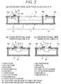
- FIGS. 2(a), 2(b), and 2(c) are cross-sectional views taken along line A-A' , line B-B', and line C-C' of FIG. 1 , respectively.
- a MOS transistor region 11, a trench isolation structure 10b, and a diode region 12 are provided on an SOI substrate including a buried oxide film 16 and a semiconductor layer 17.
- the MOS transistor region 11 includes: a P-type body region 1; an N-type drain-drift region 4 adjacent to the P-type body region 1; an N+ drain region 5 in contact with the N-type drain-drift region 4; a source region 2 formed in the P-type body region; an insulating film 13 covering the upper side of the drain-drift region 4 from an end of the source region 2; and a gate electrode 3 covering the upper side of the drain-drift region 4 from the upper end of the source region 2 through the insulating film 13.
- the trench isolation structure 10b includes an insulating film adjacent to an end portion of the P-type body region 1 and an end portion of the drain-drift region 4.
- the diode region 12 includes: a P-type anode region 6 adjacent to the trench isolation structure 10b; an N-type cathode region 8 adjacent to the trench isolation structure 10b; the insulating film 13 covering the upper side of the N-type cathode region 8 from an end of the P-type anode region 6; a diode field plate electrode 7 covering the upper side of the N-type cathode region 8 from the upper side of the P-type anode region 6 through the insulating film 13.
- FIG. 2 (b) and a cross-sectional structure of the diode region illustrated in FIG. 2(c) are identical to each other at least at a portion in contact with the trench isolation structure 10b except the N-type source region 2, a P+ body contact diffusion region 15, and a P+ anode contact diffusion region 15.
- the N+ drain region 5 and an N+ cathode contact diffusion region 9 are electrically coupled to each other through a wiring layer.
- the P+ body contact diffusion region 15 and the P+ anode contact diffusion region 14 are electrically coupled to each other through a wiring layer.
- the gate electrode 3 is electrically coupled to the diode field plate electrode 7 through a wiring layer.
- the wiring layers are not illustrated in the figures.
- pieces of electric field potential in the P-type body region 1 and the N-type drain-drift region 4 can be identical to pieces of electric field potential in the P-type anode region 6 and the N-type cathode region 8 of the diode 12, at least at a portion in proximity to the trench isolation structure 10b.
- electric field intensity to be applied to the trench isolation structure 10b becomes zero.
- electric field potential at an end portion of the MOS transistor 11 in proximity to the trench isolation structure 10b is not influenced by the trench isolation structure, and becomes identical to electric field potential at a portion other than the end portion of the MOS transistor 11.
- a drain current characteristic at the end portion of the transistor becomes equal to a drain current characteristic at a portion other than the end portion.
- An ON-withstand voltage and an OFF-withstand voltage are prevented from degrading at the end portion of the MOS transistor 11.
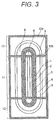
- a second embodiment of the present invention will be described based on FIG. 3 .
- a point different from the configuration in FIG. 1 is that while the gate electrode 3 of the MOS transistor 11 is coupled to the drain field plate electrode 7 of the diode 12 through the wiring layer in FIG. 1 , a gate electrode 3 is directly coupled to a drain field plate electrode in FIG. 3 . Accordingly, an effect similar to the effect that has been described in the first embodiment, is acquired.
- a third embodiment of the present invention will be described based on FIG. 4 .
- a point different from the configuration in FIG. 3 is that a gate electrode 3 and an N-type source region 2 are provided around an N+ drain region 5 and an N-type drain-drift region 4 in a MOS transistor 11 and, in response to that, a P+ anode contact diffusion region is provided around an N-type cathode region 8 of a diode 12. Accordingly, as described in the first embodiment, electric field intensity to be applied to the trench isolation structure 10b becomes zero when a voltage is applied across the transistor, and a similar effect can be acquired.
- a fourth embodiment of the present invention will be described based on FIGS. 5 and 6 .
- a point different from the configuration in FIG. 1 is that a dummy MOS transistor 18 is provided adjacent to a trench isolation structure 10b instead of the diode 12.
- a cross-sectional structure of a MOS transistor 11 in FIG. 6(b) and a cross-sectional structure of the dummy MOS transistor 18 in FIG. 6(c) are identical to each other at least at a portion in proximity to the trench isolation structure 10b.
- An N+ drain region 5 and an N+ drain region 22 of the dummy MOS transistor 18 are electrically coupled to each other through a wiring layer.
- a P+ body contact diffusion region 15, a P+ body contact diffusion region 24 of the dummy MOS transistor 18, and a gate electrode 20 of the dummy MOS transistor 18 are electrically coupled to each other through a wiring layer.
- the wiring layers are not illustrated. Accordingly, when a voltage is applied across the MOS transistor 11, pieces of electric field potential in a P-type body region 1 and an N-type drain-drift region 4 can be identical to pieces of electric field potential in the dummy MOS transistor, at least at a portion in proximity to the trench isolation structure 10b. Thus, electric field intensity to be applied to the trench isolation structure 10b becomes zero. Accordingly, the effect that has been described in the first embodiment, is acquired.
Landscapes
- Insulated Gate Type Field-Effect Transistor (AREA)
- Thin Film Transistor (AREA)
- Metal-Oxide And Bipolar Metal-Oxide Semiconductor Integrated Circuits (AREA)
- Element Separation (AREA)
Abstract
Description
- The present invention relates to a semiconductor device, and relates to a lateral semiconductor device formed on a semiconductor substrate.
- In a high-withstand-voltage lateral transistor, improvement of a layout for a plane-shaped device end portion has been conventionally performed in order to improve an ON-withstand voltage of the transistor. Here, two examples will be given and described below based on plane layout drawings in
FIGS. 7 and8 . - According to a first conventional example, as illustrated in
FIG. 7 , a P-type body region 1 envelops anN+ drain region 5 and an N-type drain-drift region 4 in a lateral NMOS transistor. Agate electrode 3 is formed so as to overlap with an end portion of the P-type body region 1. Furthermore, a semicircular and plane-shaped end portion of the P-type body region 1 has a part at which thegate electrode 3 and anN+ source region 2 are not adjacent to each other. With this structure, since an end portion of the device has nosource region 2, current density can be reduced at an end portion of thedrain region 5, and thus a problem that the drain current density increases at the end portion and a Kirk effect degrades an ON-withstand voltage, can be solved. - According to a second conventional example, as illustrated in
FIG. 8 , anN+ drain region 5 and an N-type drain-drift region 4 envelop anN+ source region 2 and a P-type body region 1 in a lateral NMOS transistor. Agate electrode 3 is formed so as to overlap with an end portion of the P-type body region 1. Furthermore, a semicircular and plane-shaped end of the P-type body region 1 has a part at which thegate electrode 3 and theN+ source region 2 are not adjacent to each other. This structure includes the N+ drain region provided on the outer circumference with respect to the N+ source region in comparison to the conventional example 1. Thus, the radius of curvature of the drain-drift region increases and drain current density at a further end portion can be reduced. Accordingly, improvement of an ON-withstand voltage can be further expected in comparison to the first conventional example. -
- Patent Literature 1:
JP 3473460 B2 - Patent Literature 2:
JP 2007-96143 A - However, although the ON-withstand voltage can be improved, each of the transistors according to the conventional examples has the following problems.
- First, ON-resistance or a drain current characteristic at the end portion of the transistor is different from ON-resistance or a drain current characteristic at the center portion, respectively. Each case of the structures according to the conventional examples includes the
N+ drain region 5 and the N-type drain region 4 also formed at the end portion and includes noN+ source region 2 provided at the end portion. Accordingly, drain resistance determined based on diffusion resistance of the N-type drain-drift region and diffusion resistance of the N+ drain region, becomes smaller at the end portion than at the center portion. As a result, the reciprocal of ON-resistance Ron or a drain current Ids does not become linear with respect to a gate width Wg, has an offset ΔWg, and is expressed by the following expression.
- Accordingly, a ratio of the offset ΔWg occupying increases in a transistor having a small gate width Wg. Accordingly, for example, in a case where the transistor is used in a current detecting (sense) circuit, a sense ratio deviates from a ratio of the gate width Wg of the transistor due to this offset. Due to the influence of the offset, a transistor having large ON-resistance and a small drain current cannot be achieved. Thus, it is difficult to constitute a current detecting circuit having a large sense ratio.
- Secondly, a variation of the ON-resistance at the end portion due to a variation in temperature is different from a variation at the center portion. The ON-resistance of the high-withstand-voltage lateral MOS transistor is mainly given by the sum of channel resistance RCH and drain-drift resistance RDRIFT, and is given by the following expression.

- Here, the channel resistance RCH and the drain-drift resistance RDRIFT each have temperature Tj dependence. However, a temperature coefficient of the channel resistance RCH and a temperature coefficient of the drain-drift resistance RDRIFT are different from each other. As described above, since the drain-drift resistance RDRIFT becomes smaller at the device end portion than at the center portion, a ratio of the drain-drift resistance occupying in the ON-resistance varies depending on the gate width Wg. As a result, a problem that temperature dependence of the ON-resistance varies depending on the gate width Wg of the transistor, occurs.
- Meanwhile, in a case where the transistor is used in a current detecting (sense) circuit, a sense ratio is given by a current amount ratio between the sense circuit and a primary (main) circuit, namely, an inverse ratio of the ON-resistance, and is given by the following expression.

- Accordingly, in a case where transistors each having a different gate width are used in a sense circuit and a main circuit, since the temperature coefficients of the pieces of ON-resistance or drain currents of the transistors, are different from each other, a problem that a sense ratio varies depending on temperature, occurs.
- The present invention provides a lateral semiconductor device having a high-withstand-voltage lateral MOS transistor structure capable of improving the above two problems.
- An object of the present invention is to equalize an ON-resistance characteristic or a drain current characteristic at a device end portion with that at a device center portion in a high-withstand-voltage lateral device. Accordingly, the current characteristic of the device can be made to be linear with respect to a width of the device, and the problems that have been described above can be solved.
- A lateral MOS transistor according to the present invention, includes: a first conductive body region formed in the semiconductor substrate layer; a second conductive drain-drift region adjacent to or apart from, and entirely enveloping the body region; a second conductive drain region in contact with the drain-drift region; a second conductive source region formed in the body region; an insulating film covering an upper side of the drain-drift region from an end of the source region; a gate electrode covering the upper side of the drain-drift region from an upper end of the source region through the insulating film; a trench isolation structure provided and including an insulating film adjacent to an end portion of the body region and an end portion of the drain-drift region; and a diode including: a first conductive anode region adjacent to the trench isolation structure; a second conductive cathode region adjacent to the trench isolation structure; an insulating film covering an upper side of the cathode region from an end of the anode region; and a diode field plate electrode covering the upper side of the cathode region from an upper side of the anode region through the insulating film. The anode region and the cathode region of the diode have impurity profiles equal to those of the body region and the drain region, respectively. In addition, a distance between a diffusion region coupling the anode region and a diffusion region coupling the cathode region, is equal to a distance between the source region and the drain region at least at a portion in contact with the trench. The anode region is electrically coupled to the body region at the same electric potential through a wiring layer. The cathode region is electrically coupled to the drain region through a wiring layer. The gate electrode is electrically coupled to the diode field plate electrode.
- Another lateral MOS transistor according to the present invention, is a lateral semiconductor device formed on a semiconductor substrate, and includes: a first conductive body region formed in the semiconductor substrate layer; a second conductive drain-drift region adjacent to or apart from, and entirely enveloping the body region; a second conductive drain region in contact with the drain-drift region; a second conductive source region formed in the body region; an insulating film covering an upper side of the drain-drift region from an end of the source region; a gate electrode covering the upper side of the drain-drift region from an upper end of the source region through the insulating film; a trench isolation structure provided and including an insulating film adjacent to an end portion of the body region and an end portion of the drain-drift region; and a dummy MOS transistor including: a first conductive second body region adjacent to the trench isolation structure; a second conductive second drain-drift region adjacent to the trench isolation structure; a second conductive second drain region in contact with the drain-drift region; a second conductive second source region formed in the body region; a second insulating film covering an upper side of the second drain-drift region from an end of the second source region; and a second gate electrode covering the upper side of the second drain-drift region from an upper side of the second source region through the second insulating film. The second body region and the second drain-drift region of the dummy MOS transistor have impurity profiles equal to those of the body region and the drain-drift region of the MOS transistor, respectively. In addition, a distance between the second source region and the second drain region of the dummy MOS transistor is equal to a distance between the source region and the drain region of the MOS transistor at least at a portion in contact with the trench isolation structure. A source electrode and a drain electrode of the dummy MOS transistor are electrically coupled to a source electrode and a drain electrode of a MOS transistor through a wiring layer, respectively. In addition, a gate electrode of the dummy MOS transistor is electrically coupled to a source electrode.
- According to the present invention, in a high-withstand-voltage lateral semiconductor device, a trench isolation structure is provided at an end portion of a body region and an end portion of a drain-drift region at a device end portion. In addition, a diode is formed adjacent to the trench isolation structure. Furthermore, the diode and a MOS transistor adjacent to the trench isolation structure have the same structure, such as an impurity profile and a size. In addition, terminals between the diode and the MOS transistor are electrically coupled. Accordingly, pieces of electric field potential of semiconductor regions in a case where a voltage is applied across individual terminals of the device, can be equal to each other through the trench isolation structure. In other words, a voltage to be applied to the trench isolation structure can be made to be zero. Accordingly, the pieces of electric field potential at the device end portion are prevented from being influenced by the trench isolation structure, and an OFF-withstand voltage does not degrade. Since a drain-drift region at an end portion that cannot be separated in a conventional structure, can be omitted, a drain current characteristic at the end portion can be made to be equal to that at a center portion. As a result, linearity of ON-resistance or a drain current of the transistor with respect to a gate width, can be improved.
- Since the drain current characteristic at the end portion can be made to be equal to that at the center portion, a temperature characteristic of the ON-resistance can be made to be constant regardless of the gate width. As a result, a variation of a sense ratio in temperature can be eliminated in a current detecting (sense) circuit having a gate width different from that of a primary (main) circuit.
- Since drain current density at the device end portion can be made to be equal to that at the center portion, it is effective for a conventional problem that drain current density at an end portion becomes larger than that at a center portion and an ON-withstand voltage degrades.
-
- [
FIG. 1] FIG. 1 is a plan view of a main portion of a high-withstand-voltage NMOS transistor according to a first embodiment of the present invention. - [
FIG. 2(a)] FIG. 2(a) is a longitudinal sectional view of a region taken along line A-A' ofFIG. 1 . - [
FIG. 2(b)] FIG. 2(b) is a longitudinal sectional view of a region taken along line B-B' ofFIG. 1 . - [
FIG. 2(C)] FIG. 2(C) is a longitudinal sectional view of a region taken along line C-C' ofFIG. 1 . - [
FIG. 3] FIG. 3 is a plan view of a main portion of a high-withstand-voltage NMOS transistor according to a second embodiment of the present invention. - [
FIG. 4] FIG. 4 is a plan view of a main portion of a high-withstand-voltage NMOS transistor according to a third embodiment of the present invention. - [
FIG. 5] FIG. 5 is a plan view of a main portion of a high-withstand-voltage NMOS transistor according to a fourth embodiment of the present invention. - [
FIG. 6(a)] FIG. 6(a) is a longitudinal sectional view of a region taken along line A-A' ofFIG. 5 . - [
FIG. 6(b)] FIG. 6(b) is a longitudinal sectional view of a region taken along line B-B' ofFIG. 5 . - [
FIG. 6(c)] FIG. 6(c) is a longitudinal sectional view of a region taken along line C-C' ofFIG. 5 . - [
FIG. 7] FIG. 7 is a plan view of a main portion of a first conventional high-withstand-voltage NMOS transistor. - [
FIG. 8] FIG. 8 is a plan view of a main portion of a second conventional high-withstand-voltage NMOS transistor. - Embodiments of the present invention will be described below based on the drawings. Note that, although a semiconductor device has been formed on a silicon on insulator (SOI) substrate in the present embodiments, the semiconductor device may be formed on an Si substrate. In addition, although a case of an NMOS transistor has been described in the present embodiments, a PMOS transistor may be applied.
- A first embodiment of the present invention will be described based on
FIGS. 1 and2 .FIG. 1 is a plan view for describing the first embodiment.FIGS. 2(a), 2(b), and 2(c) are cross-sectional views taken along line A-A' , line B-B', and line C-C' ofFIG. 1 , respectively. - As illustrated in
FIGS. 1 and2 , aMOS transistor region 11, atrench isolation structure 10b, and adiode region 12 are provided on an SOI substrate including a buriedoxide film 16 and asemiconductor layer 17. TheMOS transistor region 11 includes: a P-type body region 1; an N-type drain-drift region 4 adjacent to the P-type body region 1; anN+ drain region 5 in contact with the N-type drain-drift region 4; asource region 2 formed in the P-type body region; an insulatingfilm 13 covering the upper side of the drain-drift region 4 from an end of thesource region 2; and agate electrode 3 covering the upper side of the drain-drift region 4 from the upper end of thesource region 2 through the insulatingfilm 13. Thetrench isolation structure 10b includes an insulating film adjacent to an end portion of the P-type body region 1 and an end portion of the drain-drift region 4. Thediode region 12 includes: a P-type anode region 6 adjacent to thetrench isolation structure 10b; an N-type cathode region 8 adjacent to thetrench isolation structure 10b; the insulatingfilm 13 covering the upper side of the N-type cathode region 8 from an end of the P-type anode region 6; a diodefield plate electrode 7 covering the upper side of the N-type cathode region 8 from the upper side of the P-type anode region 6 through the insulatingfilm 13. A cross-sectional structure of the MOS transistor region illustrated inFIG. 2 (b) and a cross-sectional structure of the diode region illustrated inFIG. 2(c) are identical to each other at least at a portion in contact with thetrench isolation structure 10b except the N-type source region 2, a P+ bodycontact diffusion region 15, and a P+ anodecontact diffusion region 15. TheN+ drain region 5 and an N+ cathodecontact diffusion region 9 are electrically coupled to each other through a wiring layer. The P+ bodycontact diffusion region 15 and the P+ anodecontact diffusion region 14 are electrically coupled to each other through a wiring layer. Thegate electrode 3 is electrically coupled to the diodefield plate electrode 7 through a wiring layer. The wiring layers are not illustrated in the figures. Accordingly, when a voltage is applied across theMOS transistor 11, pieces of electric field potential in the P-type body region 1 and the N-type drain-drift region 4 can be identical to pieces of electric field potential in the P-type anode region 6 and the N-type cathode region 8 of thediode 12, at least at a portion in proximity to thetrench isolation structure 10b. Thus, electric field intensity to be applied to thetrench isolation structure 10b becomes zero. Accordingly, electric field potential at an end portion of theMOS transistor 11 in proximity to thetrench isolation structure 10b is not influenced by the trench isolation structure, and becomes identical to electric field potential at a portion other than the end portion of theMOS transistor 11. As a result, a drain current characteristic at the end portion of the transistor becomes equal to a drain current characteristic at a portion other than the end portion. An ON-withstand voltage and an OFF-withstand voltage are prevented from degrading at the end portion of theMOS transistor 11. - A second embodiment of the present invention will be described based on
FIG. 3 . A point different from the configuration inFIG. 1 is that while thegate electrode 3 of theMOS transistor 11 is coupled to the drainfield plate electrode 7 of thediode 12 through the wiring layer inFIG. 1 , agate electrode 3 is directly coupled to a drain field plate electrode inFIG. 3 . Accordingly, an effect similar to the effect that has been described in the first embodiment, is acquired. - A third embodiment of the present invention will be described based on
FIG. 4 . A point different from the configuration inFIG. 3 is that agate electrode 3 and an N-type source region 2 are provided around anN+ drain region 5 and an N-type drain-drift region 4 in aMOS transistor 11 and, in response to that, a P+ anode contact diffusion region is provided around an N-type cathode region 8 of adiode 12. Accordingly, as described in the first embodiment, electric field intensity to be applied to thetrench isolation structure 10b becomes zero when a voltage is applied across the transistor, and a similar effect can be acquired. - A fourth embodiment of the present invention will be described based on
FIGS. 5 and6 . A point different from the configuration inFIG. 1 is that adummy MOS transistor 18 is provided adjacent to atrench isolation structure 10b instead of thediode 12. A cross-sectional structure of aMOS transistor 11 inFIG. 6(b) and a cross-sectional structure of thedummy MOS transistor 18 inFIG. 6(c) are identical to each other at least at a portion in proximity to thetrench isolation structure 10b. AnN+ drain region 5 and anN+ drain region 22 of thedummy MOS transistor 18 are electrically coupled to each other through a wiring layer. A P+ bodycontact diffusion region 15, a P+ body contact diffusion region 24 of thedummy MOS transistor 18, and agate electrode 20 of thedummy MOS transistor 18 are electrically coupled to each other through a wiring layer. The wiring layers are not illustrated. Accordingly, when a voltage is applied across theMOS transistor 11, pieces of electric field potential in a P-type body region 1 and an N-type drain-drift region 4 can be identical to pieces of electric field potential in the dummy MOS transistor, at least at a portion in proximity to thetrench isolation structure 10b. Thus, electric field intensity to be applied to thetrench isolation structure 10b becomes zero. Accordingly, the effect that has been described in the first embodiment, is acquired. -
- 1 P-type body region
- 2 N-type source region
- 3 gate electrode
- 4 N-type drain-drift region
- 5 N-type drain region
- 6 P-type anode region
- 7 diode field plate region
- 8 N-type cathode region
- 9 N+ cathode contact diffusion region
- 10a trench isolation structure to be insulated from external substrate
- 10b trench isolation structure separating MOS transistor from diode
- 11 MOS transistor region
- 12 diode region
- 13 insulating film
- 14 P+ anode contact diffusion region
- 15 P+ body contact diffusion region
- 16 buried oxide film
- 17 semiconductor layer
- 18 dummy MOS transistor region
- 19 P-type body region of dummy MOS transistor
- 20 gate electrode of dummy MOS transistor
- 21 N-type drain region of dummy MOS transistor
- 22 N+ drain region of dummy MOS transistor
- 23 gate oxide film of dummy MOS transistor
- 24 P+ body contact diffusion region of dummy MOS transistor
- 25 N+ source region of dummy MOS transistor
- 26 P+ diffusion region
Claims (10)
- A lateral semiconductor device formed on a semiconductor substrate, comprising:a first conductive first region formed in the semiconductor substrate layer;a second conductive first region adjacent to or apart from, and entirely enveloping the first conductive region;a trench isolation structure provided adjacent to an end portion of the first conductive first region and an end portion of the second conductive first region, and including an insulating film;a first conductive second region adjacent to the trench isolation structure; anda second conductive second region adjacent to the trench isolation structure,wherein the first conductive first region and second region each have the same impurity profile and the same region width at least at a region adjacent to the trench isolation structure,
the second conductive first region and second region each have the same impurity profile and the same region width at least at a region adjacent to the trench isolation structure, and
the first conductive first region and the second conductive first region are regions included in a transistor. - The lateral semiconductor device according to claim 1, the lateral semiconductor device being formed on the semiconductor substrate, further comprising:a first conductive body region formed in the semiconductor substrate layer;a second conductive drain-drift region adjacent to or apart from, and entirely enveloping the body region;a second conductive drain region in contact with the drain-drift region;a second conductive source region formed in the body region;an insulating film covering an upper side of the drain-drift region from an end of the source region;a gate electrode covering the upper side of the drain-drift region from an upper end of the source region through the insulating film;a trench isolation structure provided and including an insulating film adjacent to an end portion of the body region and an end of the drain-drift region; anda diode including:a first conductive anode region adjacent to the trench isolation structure;a second conductive cathode region adjacent to the trench isolation structure; andan insulating film covering an upper side of the cathode region from an end of the anode region.
- The lateral semiconductor device according to claim 2,
wherein the anode region and the body region each have the same impurity profile,
the cathode region and the drain region each have the same impurity profile,
a distance between the source region and the drain region and a distance between a diffusion region coupling the anode region and a diffusion region coupling the cathode region, are equal to each other at least at a portion in proximity to the trench isolation structure, and
a distance of the gate electrode extending from the end of the source region to the upper side of the drain-drift region and a distance of a diode field plate electrode extending from an upper side of the anode region to the upper side of the cathode region, are equal to each other at least at a portion in proximity to the trench isolation structure. - The lateral semiconductor device according to claim 2,
wherein the anode region is electrically coupled to the body region through a wiring layer,
the cathode region is electrically coupled to the drain region through a wiring layer, and
the gate electrode is electrically coupled to the diode field plate electrode. - The lateral semiconductor device according to claim 2,
wherein the diode is formed so as to cause electric field intensity to be applied to the trench isolation structure to be zero when a voltage is applied across terminals of the lateral semiconductor device. - The lateral semiconductor device according to claim 1, the lateral semiconductor device being formed on the semiconductor substrate, further comprising:a first conductive body region formed in the semiconductor substrate layer;a second conductive drain-drift region adjacent to or apart from, and entirely enveloping the body region;a second conductive drain region in contact with the drain-drift region;a second conductive source region formed in the body region;an insulating film covering an upper side of the drain-drift region from an end of the source region;a gate electrode covering the upper side of the drain-drift region from an upper end of the source region through the insulating film;a trench isolation structure provided and including an insulating film adjacent to an end portion of the body region and an end portion of the drain-drift region; anda dummy MOS transistor including:a first conductive second body region adjacent to the trench isolation structure;a second conductive second drain-drift region adjacent to the trench isolation structure;a second conductive second drain region in contact with the drain-drift region;a second conductive second source region formed in the body region;a second insulating film covering an upper side of the second drain-drift region from an end of the second source region; anda second gate electrode covering the upper side of the second drain-drift region from an upper side of the second source region through the second insulating film.
- The lateral semiconductor device according to claim 6,
wherein the body region and the second body region each have the same impurity profile,
the drain-drift region and the second drain-drift region each have the same impurity profile,
a distance between the source region and the drain region and a distance between the second source region and the second drain region, are equal to each other at least at a portion in proximity to the trench isolation structure. - The lateral semiconductor device according to claim 6,
wherein the second body region is electrically coupled to the body region through a wiring layer,
the second drain region is electrically coupled to the drain region through a wiring layer, and
the second gate electrode is electrically coupled to the second source electrode. - The lateral semiconductor device according to claim 6,
wherein the dummy MOS transistor is formed so as to cause electric field intensity to be applied to the trench isolation structure to be zero when voltage is applied across terminals of the lateral semiconductor device. - The lateral semiconductor device according to claim 1, the lateral semiconductor device being mounted on a current detecting (sense) circuit.
Applications Claiming Priority (2)
| Application Number | Priority Date | Filing Date | Title |
|---|---|---|---|
| JP2013233622A JP6244177B2 (en) | 2013-11-12 | 2013-11-12 | Semiconductor device |
| PCT/JP2014/078012 WO2015072295A1 (en) | 2013-11-12 | 2014-10-22 | Semiconductor device |
Publications (3)
| Publication Number | Publication Date |
|---|---|
| EP3076435A1 true EP3076435A1 (en) | 2016-10-05 |
| EP3076435A4 EP3076435A4 (en) | 2017-06-07 |
| EP3076435B1 EP3076435B1 (en) | 2019-08-28 |
Family
ID=53057237
Family Applications (1)
| Application Number | Title | Priority Date | Filing Date |
|---|---|---|---|
| EP14862551.0A Active EP3076435B1 (en) | 2013-11-12 | 2014-10-22 | Semiconductor device |
Country Status (5)
| Country | Link |
|---|---|
| US (1) | US10211337B2 (en) |
| EP (1) | EP3076435B1 (en) |
| JP (1) | JP6244177B2 (en) |
| CN (1) | CN105723518B (en) |
| WO (1) | WO2015072295A1 (en) |
Cited By (1)
| Publication number | Priority date | Publication date | Assignee | Title |
|---|---|---|---|---|
| EP3327764A4 (en) * | 2015-07-17 | 2019-03-20 | Hitachi Automotive Systems, Ltd. | SWITCHING ELEMENT AND CHARGE ATTACK DEVICE |
Families Citing this family (13)
| Publication number | Priority date | Publication date | Assignee | Title |
|---|---|---|---|---|
| US10546816B2 (en) * | 2015-12-10 | 2020-01-28 | Nexperia B.V. | Semiconductor substrate with electrically isolating dielectric partition |
| ITUA20161531A1 (en) * | 2016-03-10 | 2017-09-10 | St Microelectronics Srl | DIODE WITH REDUCED RECOVERY TIME FOR APPLICATIONS SUBJECT TO THE CURRENT RECIRCULATION PHENOMENON AND / OR TO RAPID VOLTAGE VARIATIONS |
| WO2018110141A1 (en) * | 2016-12-14 | 2018-06-21 | 日立オートモティブシステムズ株式会社 | Load drive device |
| JP7153559B2 (en) * | 2017-07-14 | 2022-10-14 | ヌヴォトンテクノロジージャパン株式会社 | semiconductor equipment |
| CN110612598B (en) * | 2018-04-16 | 2023-02-14 | 新唐科技日本株式会社 | Semiconductor device with a plurality of semiconductor chips |
| JP7000240B2 (en) * | 2018-04-18 | 2022-01-19 | ルネサスエレクトロニクス株式会社 | Semiconductor device |
| JP7569144B2 (en) * | 2018-12-19 | 2024-10-17 | エイブリック株式会社 | Semiconductor Device |
| EP3850670B1 (en) * | 2019-02-28 | 2024-04-03 | Yangtze Memory Technologies Co., Ltd. | High-voltage semiconductor device with increased breakdown voltage and manufacturing method thereof |
| US12598799B2 (en) * | 2021-08-31 | 2026-04-07 | Texas Instruments Incorporated | High voltage finger layout transistor |
| EP4174922A1 (en) | 2021-10-29 | 2023-05-03 | Infineon Technologies Austria AG | High-voltage semiconductor device |
| EP4220697A1 (en) * | 2022-01-27 | 2023-08-02 | Infineon Technologies Austria AG | Semiconductor device with trench isolation structures in a transition region and method of manufacturing |
| CN116666450B (en) * | 2022-02-17 | 2026-05-29 | 立锜科技股份有限公司 | High-voltage element and method for manufacturing same |
| CN116169177B (en) * | 2023-04-06 | 2026-05-12 | 杭州电子科技大学温州研究院有限公司 | Trench SOI-LDMOS transistor with control region |
Family Cites Families (17)
| Publication number | Priority date | Publication date | Assignee | Title |
|---|---|---|---|---|
| JPH10154812A (en) * | 1996-09-30 | 1998-06-09 | Toshiba Corp | High voltage semiconductor device |
| JP3237555B2 (en) | 1997-01-09 | 2001-12-10 | 富士電機株式会社 | Semiconductor device |
| JP3473460B2 (en) | 1998-11-20 | 2003-12-02 | 富士電機株式会社 | Horizontal semiconductor device |
| JP2003007843A (en) * | 2001-06-20 | 2003-01-10 | Toshiba Corp | Semiconductor device |
| US7719054B2 (en) * | 2006-05-31 | 2010-05-18 | Advanced Analogic Technologies, Inc. | High-voltage lateral DMOS device |
| JP4342498B2 (en) | 2005-09-30 | 2009-10-14 | パナソニック株式会社 | Horizontal semiconductor device |
| US7670908B2 (en) * | 2007-01-22 | 2010-03-02 | Alpha & Omega Semiconductor, Ltd. | Configuration of high-voltage semiconductor power device to achieve three dimensional charge coupling |
| JP2008235856A (en) | 2007-02-22 | 2008-10-02 | Matsushita Electric Ind Co Ltd | Semiconductor device |
| JP5162186B2 (en) * | 2007-08-27 | 2013-03-13 | トヨタ自動車株式会社 | Manufacturing method of semiconductor device |
| JP5407398B2 (en) * | 2009-02-12 | 2014-02-05 | 富士電機株式会社 | Semiconductor device |
| JP2011061051A (en) | 2009-09-11 | 2011-03-24 | Toyota Motor Corp | Semiconductor device |
| US20110260245A1 (en) * | 2010-04-23 | 2011-10-27 | Taiwan Semiconductor Manufacturing Company, Ltd. | Cost Effective Global Isolation and Power Dissipation For Power Integrated Circuit Device |
| DE102011076610A1 (en) * | 2010-06-04 | 2011-12-08 | Denso Corporation | CURRENT SENSOR, INVERTER CIRCUIT AND THIS EXPOSED SEMICONDUCTOR DEVICE |
| JP5488256B2 (en) * | 2010-06-25 | 2014-05-14 | 三菱電機株式会社 | Power semiconductor device |
| JP2012028451A (en) * | 2010-07-21 | 2012-02-09 | Hitachi Ltd | Semiconductor integrated circuit |
| TWI449159B (en) * | 2011-04-18 | 2014-08-11 | Episil Technologies Inc | Power lateral double diffused MOS device |
| JP5672500B2 (en) * | 2011-10-18 | 2015-02-18 | トヨタ自動車株式会社 | Semiconductor device |
-
2013
- 2013-11-12 JP JP2013233622A patent/JP6244177B2/en active Active
-
2014
- 2014-10-22 WO PCT/JP2014/078012 patent/WO2015072295A1/en not_active Ceased
- 2014-10-22 EP EP14862551.0A patent/EP3076435B1/en active Active
- 2014-10-22 US US15/034,286 patent/US10211337B2/en active Active
- 2014-10-22 CN CN201480061640.1A patent/CN105723518B/en active Active
Cited By (1)
| Publication number | Priority date | Publication date | Assignee | Title |
|---|---|---|---|---|
| EP3327764A4 (en) * | 2015-07-17 | 2019-03-20 | Hitachi Automotive Systems, Ltd. | SWITCHING ELEMENT AND CHARGE ATTACK DEVICE |
Also Published As
| Publication number | Publication date |
|---|---|
| US20160276477A1 (en) | 2016-09-22 |
| CN105723518B (en) | 2018-10-02 |
| EP3076435A4 (en) | 2017-06-07 |
| WO2015072295A1 (en) | 2015-05-21 |
| CN105723518A (en) | 2016-06-29 |
| JP2015095531A (en) | 2015-05-18 |
| JP6244177B2 (en) | 2017-12-06 |
| US10211337B2 (en) | 2019-02-19 |
| EP3076435B1 (en) | 2019-08-28 |
Similar Documents
| Publication | Publication Date | Title |
|---|---|---|
| US10211337B2 (en) | Semiconductor device | |
| US11131693B2 (en) | Vertical sense devices in vertical trench MOSFET | |
| US9741788B2 (en) | Semiconductor device and method for fabricating the same | |
| US9231083B2 (en) | High breakdown voltage LDMOS device | |
| US9722072B2 (en) | Manufacturing method of high-voltage metal-oxide-semiconductor transistor | |
| US8637928B2 (en) | Semiconductor device | |
| US10096700B2 (en) | Power semiconductor device comprising trench structures | |
| US20100078682A1 (en) | Power mosfet having a strained channel in a semiconductor heterostructure on metal substrate | |
| US10944001B1 (en) | Deep trench and junction hybrid isolation | |
| US20130307609A1 (en) | Hall Effect Device | |
| US9099551B2 (en) | Lateral high-voltage transistor and method for manufacturing the same | |
| US20210083089A1 (en) | Semiconductor device | |
| JP7153559B2 (en) | semiconductor equipment | |
| JP6678615B2 (en) | Semiconductor device | |
| US9825168B2 (en) | Semiconductor device capable of high-voltage operation | |
| CN119153538A (en) | Semiconductor structure and semiconductor device | |
| JP5446404B2 (en) | Semiconductor device | |
| KR20250167634A (en) | semiconductor devices |
Legal Events
| Date | Code | Title | Description |
|---|---|---|---|
| PUAI | Public reference made under article 153(3) epc to a published international application that has entered the european phase |
Free format text: ORIGINAL CODE: 0009012 |
|
| 17P | Request for examination filed |
Effective date: 20160613 |
|
| AK | Designated contracting states |
Kind code of ref document: A1 Designated state(s): AL AT BE BG CH CY CZ DE DK EE ES FI FR GB GR HR HU IE IS IT LI LT LU LV MC MK MT NL NO PL PT RO RS SE SI SK SM TR |
|
| AX | Request for extension of the european patent |
Extension state: BA ME |
|
| DAX | Request for extension of the european patent (deleted) | ||
| RIN1 | Information on inventor provided before grant (corrected) |
Inventor name: WADA, SHINICHIROU |
|
| REG | Reference to a national code |
Ref country code: DE Ref legal event code: R079 Ref document number: 602014052728 Country of ref document: DE Free format text: PREVIOUS MAIN CLASS: H01L0029786000 Ipc: H01L0021336000 |
|
| A4 | Supplementary search report drawn up and despatched |
Effective date: 20170508 |
|
| RIC1 | Information provided on ipc code assigned before grant |
Ipc: H01L 21/336 20060101AFI20170428BHEP Ipc: H01L 29/868 20060101ALI20170428BHEP Ipc: H01L 29/786 20060101ALI20170428BHEP Ipc: H01L 21/76 20060101ALI20170428BHEP Ipc: H01L 29/06 20060101ALI20170428BHEP Ipc: H01L 29/78 20060101ALI20170428BHEP Ipc: H01L 29/861 20060101ALI20170428BHEP |
|
| STAA | Information on the status of an ep patent application or granted ep patent |
Free format text: STATUS: EXAMINATION IS IN PROGRESS |
|
| 17Q | First examination report despatched |
Effective date: 20180201 |
|
| GRAP | Despatch of communication of intention to grant a patent |
Free format text: ORIGINAL CODE: EPIDOSNIGR1 |
|
| STAA | Information on the status of an ep patent application or granted ep patent |
Free format text: STATUS: GRANT OF PATENT IS INTENDED |
|
| RIN1 | Information on inventor provided before grant (corrected) |
Inventor name: WADA, SHINICHIROU |
|
| INTG | Intention to grant announced |
Effective date: 20190416 |
|
| GRAS | Grant fee paid |
Free format text: ORIGINAL CODE: EPIDOSNIGR3 |
|
| GRAA | (expected) grant |
Free format text: ORIGINAL CODE: 0009210 |
|
| STAA | Information on the status of an ep patent application or granted ep patent |
Free format text: STATUS: THE PATENT HAS BEEN GRANTED |
|
| AK | Designated contracting states |
Kind code of ref document: B1 Designated state(s): AL AT BE BG CH CY CZ DE DK EE ES FI FR GB GR HR HU IE IS IT LI LT LU LV MC MK MT NL NO PL PT RO RS SE SI SK SM TR |
|
| REG | Reference to a national code |
Ref country code: GB Ref legal event code: FG4D |
|
| REG | Reference to a national code |
Ref country code: CH Ref legal event code: EP |
|
| REG | Reference to a national code |
Ref country code: AT Ref legal event code: REF Ref document number: 1173452 Country of ref document: AT Kind code of ref document: T Effective date: 20190915 |
|
| REG | Reference to a national code |
Ref country code: IE Ref legal event code: FG4D |
|
| REG | Reference to a national code |
Ref country code: DE Ref legal event code: R096 Ref document number: 602014052728 Country of ref document: DE |
|
| REG | Reference to a national code |
Ref country code: NL Ref legal event code: MP Effective date: 20190828 |
|
| REG | Reference to a national code |
Ref country code: LT Ref legal event code: MG4D |
|
| PG25 | Lapsed in a contracting state [announced via postgrant information from national office to epo] |
Ref country code: BG Free format text: LAPSE BECAUSE OF FAILURE TO SUBMIT A TRANSLATION OF THE DESCRIPTION OR TO PAY THE FEE WITHIN THE PRESCRIBED TIME-LIMIT Effective date: 20191128 Ref country code: NL Free format text: LAPSE BECAUSE OF FAILURE TO SUBMIT A TRANSLATION OF THE DESCRIPTION OR TO PAY THE FEE WITHIN THE PRESCRIBED TIME-LIMIT Effective date: 20190828 Ref country code: PT Free format text: LAPSE BECAUSE OF FAILURE TO SUBMIT A TRANSLATION OF THE DESCRIPTION OR TO PAY THE FEE WITHIN THE PRESCRIBED TIME-LIMIT Effective date: 20191230 Ref country code: LT Free format text: LAPSE BECAUSE OF FAILURE TO SUBMIT A TRANSLATION OF THE DESCRIPTION OR TO PAY THE FEE WITHIN THE PRESCRIBED TIME-LIMIT Effective date: 20190828 Ref country code: HR Free format text: LAPSE BECAUSE OF FAILURE TO SUBMIT A TRANSLATION OF THE DESCRIPTION OR TO PAY THE FEE WITHIN THE PRESCRIBED TIME-LIMIT Effective date: 20190828 Ref country code: NO Free format text: LAPSE BECAUSE OF FAILURE TO SUBMIT A TRANSLATION OF THE DESCRIPTION OR TO PAY THE FEE WITHIN THE PRESCRIBED TIME-LIMIT Effective date: 20191128 Ref country code: SE Free format text: LAPSE BECAUSE OF FAILURE TO SUBMIT A TRANSLATION OF THE DESCRIPTION OR TO PAY THE FEE WITHIN THE PRESCRIBED TIME-LIMIT Effective date: 20190828 Ref country code: FI Free format text: LAPSE BECAUSE OF FAILURE TO SUBMIT A TRANSLATION OF THE DESCRIPTION OR TO PAY THE FEE WITHIN THE PRESCRIBED TIME-LIMIT Effective date: 20190828 |
|
| PG25 | Lapsed in a contracting state [announced via postgrant information from national office to epo] |
Ref country code: ES Free format text: LAPSE BECAUSE OF FAILURE TO SUBMIT A TRANSLATION OF THE DESCRIPTION OR TO PAY THE FEE WITHIN THE PRESCRIBED TIME-LIMIT Effective date: 20190828 Ref country code: GR Free format text: LAPSE BECAUSE OF FAILURE TO SUBMIT A TRANSLATION OF THE DESCRIPTION OR TO PAY THE FEE WITHIN THE PRESCRIBED TIME-LIMIT Effective date: 20191129 Ref country code: IS Free format text: LAPSE BECAUSE OF FAILURE TO SUBMIT A TRANSLATION OF THE DESCRIPTION OR TO PAY THE FEE WITHIN THE PRESCRIBED TIME-LIMIT Effective date: 20191228 Ref country code: RS Free format text: LAPSE BECAUSE OF FAILURE TO SUBMIT A TRANSLATION OF THE DESCRIPTION OR TO PAY THE FEE WITHIN THE PRESCRIBED TIME-LIMIT Effective date: 20190828 Ref country code: AL Free format text: LAPSE BECAUSE OF FAILURE TO SUBMIT A TRANSLATION OF THE DESCRIPTION OR TO PAY THE FEE WITHIN THE PRESCRIBED TIME-LIMIT Effective date: 20190828 Ref country code: LV Free format text: LAPSE BECAUSE OF FAILURE TO SUBMIT A TRANSLATION OF THE DESCRIPTION OR TO PAY THE FEE WITHIN THE PRESCRIBED TIME-LIMIT Effective date: 20190828 |
|
| REG | Reference to a national code |
Ref country code: AT Ref legal event code: MK05 Ref document number: 1173452 Country of ref document: AT Kind code of ref document: T Effective date: 20190828 |
|
| PG25 | Lapsed in a contracting state [announced via postgrant information from national office to epo] |
Ref country code: TR Free format text: LAPSE BECAUSE OF FAILURE TO SUBMIT A TRANSLATION OF THE DESCRIPTION OR TO PAY THE FEE WITHIN THE PRESCRIBED TIME-LIMIT Effective date: 20190828 |
|
| PG25 | Lapsed in a contracting state [announced via postgrant information from national office to epo] |
Ref country code: RO Free format text: LAPSE BECAUSE OF FAILURE TO SUBMIT A TRANSLATION OF THE DESCRIPTION OR TO PAY THE FEE WITHIN THE PRESCRIBED TIME-LIMIT Effective date: 20190828 Ref country code: EE Free format text: LAPSE BECAUSE OF FAILURE TO SUBMIT A TRANSLATION OF THE DESCRIPTION OR TO PAY THE FEE WITHIN THE PRESCRIBED TIME-LIMIT Effective date: 20190828 Ref country code: IT Free format text: LAPSE BECAUSE OF FAILURE TO SUBMIT A TRANSLATION OF THE DESCRIPTION OR TO PAY THE FEE WITHIN THE PRESCRIBED TIME-LIMIT Effective date: 20190828 Ref country code: AT Free format text: LAPSE BECAUSE OF FAILURE TO SUBMIT A TRANSLATION OF THE DESCRIPTION OR TO PAY THE FEE WITHIN THE PRESCRIBED TIME-LIMIT Effective date: 20190828 Ref country code: DK Free format text: LAPSE BECAUSE OF FAILURE TO SUBMIT A TRANSLATION OF THE DESCRIPTION OR TO PAY THE FEE WITHIN THE PRESCRIBED TIME-LIMIT Effective date: 20190828 Ref country code: PL Free format text: LAPSE BECAUSE OF FAILURE TO SUBMIT A TRANSLATION OF THE DESCRIPTION OR TO PAY THE FEE WITHIN THE PRESCRIBED TIME-LIMIT Effective date: 20190828 |
|
| PG25 | Lapsed in a contracting state [announced via postgrant information from national office to epo] |
Ref country code: CZ Free format text: LAPSE BECAUSE OF FAILURE TO SUBMIT A TRANSLATION OF THE DESCRIPTION OR TO PAY THE FEE WITHIN THE PRESCRIBED TIME-LIMIT Effective date: 20190828 Ref country code: SK Free format text: LAPSE BECAUSE OF FAILURE TO SUBMIT A TRANSLATION OF THE DESCRIPTION OR TO PAY THE FEE WITHIN THE PRESCRIBED TIME-LIMIT Effective date: 20190828 Ref country code: MC Free format text: LAPSE BECAUSE OF FAILURE TO SUBMIT A TRANSLATION OF THE DESCRIPTION OR TO PAY THE FEE WITHIN THE PRESCRIBED TIME-LIMIT Effective date: 20190828 Ref country code: SM Free format text: LAPSE BECAUSE OF FAILURE TO SUBMIT A TRANSLATION OF THE DESCRIPTION OR TO PAY THE FEE WITHIN THE PRESCRIBED TIME-LIMIT Effective date: 20190828 Ref country code: IS Free format text: LAPSE BECAUSE OF FAILURE TO SUBMIT A TRANSLATION OF THE DESCRIPTION OR TO PAY THE FEE WITHIN THE PRESCRIBED TIME-LIMIT Effective date: 20200224 |
|
| REG | Reference to a national code |
Ref country code: CH Ref legal event code: PL |
|
| REG | Reference to a national code |
Ref country code: DE Ref legal event code: R097 Ref document number: 602014052728 Country of ref document: DE |
|
| PLBE | No opposition filed within time limit |
Free format text: ORIGINAL CODE: 0009261 |
|
| STAA | Information on the status of an ep patent application or granted ep patent |
Free format text: STATUS: NO OPPOSITION FILED WITHIN TIME LIMIT |
|
| PG2D | Information on lapse in contracting state deleted |
Ref country code: IS |
|
| PG25 | Lapsed in a contracting state [announced via postgrant information from national office to epo] |
Ref country code: LI Free format text: LAPSE BECAUSE OF NON-PAYMENT OF DUE FEES Effective date: 20191031 Ref country code: LU Free format text: LAPSE BECAUSE OF NON-PAYMENT OF DUE FEES Effective date: 20191022 Ref country code: CH Free format text: LAPSE BECAUSE OF NON-PAYMENT OF DUE FEES Effective date: 20191031 |
|
| 26N | No opposition filed |
Effective date: 20200603 |
|
| REG | Reference to a national code |
Ref country code: BE Ref legal event code: MM Effective date: 20191031 |
|
| PG25 | Lapsed in a contracting state [announced via postgrant information from national office to epo] |
Ref country code: BE Free format text: LAPSE BECAUSE OF NON-PAYMENT OF DUE FEES Effective date: 20191031 Ref country code: SI Free format text: LAPSE BECAUSE OF FAILURE TO SUBMIT A TRANSLATION OF THE DESCRIPTION OR TO PAY THE FEE WITHIN THE PRESCRIBED TIME-LIMIT Effective date: 20190828 |
|
| GBPC | Gb: european patent ceased through non-payment of renewal fee |
Effective date: 20191128 |
|
| PG25 | Lapsed in a contracting state [announced via postgrant information from national office to epo] |
Ref country code: FR Free format text: LAPSE BECAUSE OF NON-PAYMENT OF DUE FEES Effective date: 20191028 Ref country code: IE Free format text: LAPSE BECAUSE OF NON-PAYMENT OF DUE FEES Effective date: 20191022 Ref country code: GB Free format text: LAPSE BECAUSE OF NON-PAYMENT OF DUE FEES Effective date: 20191128 |
|
| REG | Reference to a national code |
Ref country code: DE Ref legal event code: R082 Ref document number: 602014052728 Country of ref document: DE Representative=s name: MERH-IP MATIAS ERNY REICHL HOFFMANN PATENTANWA, DE Ref country code: DE Ref legal event code: R081 Ref document number: 602014052728 Country of ref document: DE Owner name: HITACHI ASTEMO, LTD., HITACHINAKA-SHI, JP Free format text: FORMER OWNER: HITACHI AUTOMOTIVE SYSTEMS, LTD., HITACHINAKA-SHI, IBARAKI, JP |
|
| PG25 | Lapsed in a contracting state [announced via postgrant information from national office to epo] |
Ref country code: CY Free format text: LAPSE BECAUSE OF FAILURE TO SUBMIT A TRANSLATION OF THE DESCRIPTION OR TO PAY THE FEE WITHIN THE PRESCRIBED TIME-LIMIT Effective date: 20190828 |
|
| PG25 | Lapsed in a contracting state [announced via postgrant information from national office to epo] |
Ref country code: MT Free format text: LAPSE BECAUSE OF FAILURE TO SUBMIT A TRANSLATION OF THE DESCRIPTION OR TO PAY THE FEE WITHIN THE PRESCRIBED TIME-LIMIT Effective date: 20190828 Ref country code: HU Free format text: LAPSE BECAUSE OF FAILURE TO SUBMIT A TRANSLATION OF THE DESCRIPTION OR TO PAY THE FEE WITHIN THE PRESCRIBED TIME-LIMIT; INVALID AB INITIO Effective date: 20141022 |
|
| PG25 | Lapsed in a contracting state [announced via postgrant information from national office to epo] |
Ref country code: MK Free format text: LAPSE BECAUSE OF FAILURE TO SUBMIT A TRANSLATION OF THE DESCRIPTION OR TO PAY THE FEE WITHIN THE PRESCRIBED TIME-LIMIT Effective date: 20190828 |
|
| REG | Reference to a national code |
Ref country code: DE Ref legal event code: R079 Ref document number: 602014052728 Country of ref document: DE Free format text: PREVIOUS MAIN CLASS: H01L0021336000 Ipc: H10D0030010000 |
|
| PGFP | Annual fee paid to national office [announced via postgrant information from national office to epo] |
Ref country code: DE Payment date: 20250902 Year of fee payment: 12 |