EP3074792B1 - Röntgen- und gammastrahlendetektor - Google Patents
Röntgen- und gammastrahlendetektor Download PDFInfo
- Publication number
- EP3074792B1 EP3074792B1 EP14802681.8A EP14802681A EP3074792B1 EP 3074792 B1 EP3074792 B1 EP 3074792B1 EP 14802681 A EP14802681 A EP 14802681A EP 3074792 B1 EP3074792 B1 EP 3074792B1
- Authority
- EP
- European Patent Office
- Prior art keywords
- electrodes
- detector
- drift
- strip electrodes
- axis
- Prior art date
- Legal status (The legal status is an assumption and is not a legal conclusion. Google has not performed a legal analysis and makes no representation as to the accuracy of the status listed.)
- Active
Links
Images

Classifications
-
- G—PHYSICS
- G01—MEASURING; TESTING
- G01T—MEASUREMENT OF NUCLEAR OR X-RADIATION
- G01T1/00—Measuring X-radiation, gamma radiation, corpuscular radiation, or cosmic radiation
- G01T1/16—Measuring radiation intensity
- G01T1/24—Measuring radiation intensity with semiconductor detectors
- G01T1/241—Electrode arrangements, e.g. continuous or parallel strips or the like
-
- G—PHYSICS
- G01—MEASURING; TESTING
- G01T—MEASUREMENT OF NUCLEAR OR X-RADIATION
- G01T1/00—Measuring X-radiation, gamma radiation, corpuscular radiation, or cosmic radiation
- G01T1/16—Measuring radiation intensity
- G01T1/161—Applications in the field of nuclear medicine, e.g. in vivo counting
-
- G—PHYSICS
- G01—MEASURING; TESTING
- G01T—MEASUREMENT OF NUCLEAR OR X-RADIATION
- G01T1/00—Measuring X-radiation, gamma radiation, corpuscular radiation, or cosmic radiation
- G01T1/16—Measuring radiation intensity
- G01T1/24—Measuring radiation intensity with semiconductor detectors
- G01T1/247—Detector read-out circuitry
-
- H—ELECTRICITY
- H01—ELECTRIC ELEMENTS
- H01Q—ANTENNAS, i.e. RADIO AERIALS
- H01Q1/00—Details of, or arrangements associated with, antennas
- H01Q1/27—Adaptation for use in or on movable bodies
- H01Q1/28—Adaptation for use in or on aircraft, missiles, satellites, or balloons
- H01Q1/288—Satellite antennas
Definitions
- the present invention relates to a semiconductor radiation detector for detecting X-ray and / or gamma-ray radiation.
- the invention further relates to a method for, along a first axis, estimating a location of an interaction between an X-ray or gamma-ray photon and a converter element.
- Detection of X-rays and gamma-rays has a large number of important applications such as national security, medical imaging, astrophysics, and gamma-ray spectroscopy.
- CZT Cadmium Zinc Telluride
- US20100252744 discloses a room temperature radiation detector that comprises a converter element and a plurality of electrode systems arranged on said element, wherein each electrode system comprises a primary electrode and a supplementary electrode, which are connected to a readout circuitry.
- the primary and the supplementary electrodes may particularly be realized by planar, parallel stripes extending in a common plane, wherein said stripes are electrically connected above said plane.
- US6002134 discloses cross-strip radiation detector for detecting ionizing radiation comprising an array of anodes and a single control electrode common to all anodes.
- each detector electrode By providing each detector electrode with a readout channel the spatial location of the event within the converter element may be estimated.
- the invention relates to a semiconductor radiation detector for detecting X-ray and / or gamma-ray radiation comprising:
- the increased resolution of the detector may be used to increase the resolution of the imaging modality, i.e. the resolution of CT images slices or the resolution of PET images. This may reduce the risk that the medical doctor misses pathological conditions when examining the images.
- the detector may be configured to detect X-rays or gamma-rays having energies between 10 keV and 3000keV, or between 20 keV and 2000 keV.
- the converter element may be a heavy compound semiconductor such as Cadmium Zinc Telluride (CZT), CdMnTe, HgI, TIBr, HgCdTe, PbI, InP, and GaAs.
- the converter element may have a height between 1 mm and 20 mm, 2mm and 8mm or 2.5mm and 7.5mm.
- the height of the converter element is defined as the distance between the first side and the second side of the converter element.
- the one or more cathodes are negatively biased relative to the plurality of detector electrodes..
- the pitch (P) may be between 0.25 mm and 20 mm, between 0.5 mm and 10 mm, or between 1 mm and 4 mm.
- the detector may comprise one or more voltage sources.
- the amount of bias provided to each drift electrode may be dependent on the distance from the drift electrode to its nearest detector electrode, e.g. drift electrodes positioned close to a detector electrode may be supplied with a potential being less negative relative to the potential of the detector electrodes than drift electrodes positioned further away. This may improve the steering of the electrons.
- An event is defined as the interaction between an X-ray or gamma-ray photon and an electron in the converter element creating an electron / hole pair.
- the processing unit may be configured to detect the event by processing signals obtained from said detector electrodes, said drift electrodes, or both said detector electrodes and said drift electrodes.
- the processing unit may simultaneously detect the event and estimate the position. Alternatively, the processing unit may firstly detect the event and secondly estimate the position.
- said plurality of detector electrodes are elongated parallel detector strip electrodes having a width (W1), and a length (L1) extending along a second axis being perpendicular to said first axis, the pitch (P) being the pitch between two neighbouring strips;
- said plurality of drift electrodes are elongated parallel drift strip electrodes having a width (W2), and a length (L2); and wherein at least one drift strip electrode is arranged between any two neighbouring detector strip electrodes.
- L1 is preferably significantly larger than W1 such as at least 10 times larger or at least 50 times larger.
- L2 is preferably significantly larger than W2 such as at least 10 times larger or at least 50 times larger.
- the drift strip electrodes are also extending along the second axis, i.e. both the detector strip electrodes and the drift strip electrodes are arranged parallel with the second axis and perpendicular with the first axis.
- the pitch (P) is preferably significantly larger than the W1 such as at least 2 times larger, or at least 4 times larger.
- the pitch (P) is preferably significantly larger than W2 such as at least 2 times larger, or at least 4 times larger.
- L1 and L2 may be of equal length.
- a detector having a high spectral resolution is provided.
- the spectral performance may be improved further using the estimate of the location along the first axis. This is achieved by correction for electron trapping in the converter element, the effect of which can be measured and characterized as function of location (first axis) with the help of mono energetic X and gamma-ray sources.
- the improvement is dependent on the precision of the estimate, thus the improved spatial resolution of by the present invention may further result in an improved spectral resolution.
- said readout circuitry is further configured to read out signals from said at least one cathode; and said processing unit is further configured to estimate the location of said event along a third axis being perpendicular to both said first axis and said second axis, by processing one or more signals obtained from said detector strip electrodes together with one or more signals obtained from said at least one cathode, wherein said processing unit is configured to estimate the location of said event along said first axis by processing signals obtained from said detector strip electrodes and said drift strip electrodes together with said estimate of said location of said event along said third axis.
- a calibration constant dependent on the estimated location of said event along said third axis may be used. This may result in a more precise result and further improve the linearity of the semiconductor radiation detector along the first axis.
- the location of the event along the third axis i.e. the depth information (also called depth sensing) can be derived from the ratio R ⁇ Qp/Qs, where Qp is the cathode signal and Qs the detector strip signal.
- Qp is the cathode signal and Qs the detector strip signal.
- At least two drift strip electrodes are arranged between any two neighbouring detector strip electrodes.
- At least three drift strip electrodes are arranged between any two neighbouring detector strip electrodes.
- the steering / focusing of the electron may be improved.
- said processing unit is configured to make a first estimate of said location of said event along said first axis with a first spatial resolution by processing signals obtained from said detector strip electrodes, and a second estimate of said location of said event along said first axis with a second spatial resolution being higher than said first spatial resolution by additionally processing signals obtained from said drift strip electrodes.
- the processing unit may be configured to continuously monitor signals from the detector strip electrodes, and, when an event is detected, control the readout circuitry to record signals from both the detector strip electrodes and the drift strip electrodes.
- the processing unit may be configured to find the detector strip being closest to the event. The position along the first axis of the found detector strip electrode may be the first estimate of the location of the event.
- the value (D R , D L ) may be the maximum value of the signal, the minimum value of the signal, the average value of the signal or similar.
- the values may comprise a plurality of components.
- (D R , D L ) each is summation of two components, a first component being a maximum value, and a second component being a absolute of the minimum value of the respective drift signals.
- the calibration constant C is selected dependent on an estimated location of said event along said third axis(the depth of interaction), whereby different calibration constants may be used for different estimated location of said event along said third axis.
- the precision and the linearity of the semiconductor radiation detector along the first axis may be improved.
- the calibration constant C may be determined by illuminating the detector with a photon beam having a known beam profile at a plurality of known positions. A calibration constant may then be found that fulfills a predetermined requirement such as a lowest summed absolute error, a lowest summed squared error etc. This may be done by making an extensive search within a delimited region as is well known to the skilled person.
- each detector strip electrode is provided with a unique readout channel from said readout circuitry; said plurality of drift strip electrodes is grouped into a plurality of groups of drift strip electrodes, each group comprising at least two drift strip electrodes; and each group of drift strip electrodes are provided with a common readout channel from said readout circuitry.
- the number of required readout channels may be significantly reduced. This lowers the complexity and cost of the readout circuitry and further reduces the processing load of the processing unit.
- said plurality of drift strip electrodes is grouped into at least 3 groups or at least 4 groups.
- each particular group of drift strip electrodes comprises:
- the signals read out from the groups of drift strip electrodes may be used to make a precise estimate of the location of the event.
- the pitch (P2) between the subgroups for all groups of drift strip electrodes is at least four times the pitch (P) between the detector strip electrodes.
- a plurality of elongated parallel cathode strips are arranged on said first side of said converter element extending along said first axis, said parallel cathode strips having a width (W3) and a length (L3), and are arranged with a pitch (P3) along said second axis; said readout circuitry is further configured to read out signals from said plurality of cathode strips; and said processing unit is further configured to estimate a location of said event along said second axis by processing signals obtained from said plurality of cathode strips.
- the detector may provide a two-dimensional estimate of the location of the event.
- the processing unit may estimate the location of the event along the second axis by interpolating the cathode signal having the highest amplitude with its two neighbours. This may be done by fitting a polynomial and finding the location of the peak of the polynomial.
- said processing unit is further configured to estimate the depth of said event, by processing one or more signals obtained from said detector strip electrodes together with one or more signals obtained from said cathode strips.
- the depth information (also called depth sensing) can be derived from the ratio R ⁇ Qp/Qs, where Qp is the cathode signal and Qs the detector strip signal.
- Qp is the cathode signal
- Qs the detector strip signal.
- the invention relates to a method for, along a first axis, estimating a location of an interaction between an X-ray or gamma-ray photon and a converter element, said converter element converting incident X-ray and gamma-ray photons into electron-hole pairs, said converter element comprising a first side and a second side, said second side being opposite to said first side, the method comprising the steps of:
- At least one cathode is preferably arranged on said first side of said converter element.
- said plurality of detector electrodes are elongated parallel detector strip electrodes having a width (W1), and a length (L1), the pitch (P) being the pitch between two neighbouring strips; said plurality of drift electrodes are elongated parallel drift strip electrodes having a width (W2), and a length (L2); and wherein at least one drift strip electrode is arranged between any two neighbouring detector strip electrodes.
- At least one cathodes is arranged on said first side of said converter element, wherein said method further comprises the steps of:
- a first estimate of the location of the event in said first dimension is made by processing signals obtained from said detector strip electrodes, said first estimate having a first spatial resolution; and a second estimate of the location of the event in said first dimension is made by additionally processing signals obtained from said drift strip electrodes, said second estimate having a second spatial resolution being higher than said first spatial resolution.
- the calibration constant C is selected dependent on an estimated location of said event along said third axis(the depth of interaction), whereby different calibration constants may be used for different estimated location of said event along said third axis.
- the invention relates to use of a radiation detector as disclosed in relation to the first aspect of the invention in:
- the term 'processing unit' is intended to comprise any circuit and/or device suitably adapted to perform the functions described herein.
- the above term comprises general purpose or proprietary programmable microprocessors, Digital Signal Processors (DSP), Application Specific Integrated Circuits (ASIC), Programmable Logic Arrays (PLA), Field Programmable Gate Arrays (FPGA), special-purpose electronic circuits, etc. or a combination thereof
- the different aspects of the present invention can be implemented in different ways including as a radiation detector and as a method for, along a first axis, estimating a location of an interaction between an X-ray or gamma-ray photon and a converter element as described above and in the following, each yielding one or more of the benefits and advantages described in connection with at least one of the aspects described above, and each having one or more preferred embodiments corresponding to the preferred embodiments described in connection with at least one of the aspects described above and/or disclosed in the dependant claims.
- embodiments described in connection with one of the aspects described herein may equally be applied to the other aspects.
- Fig. 1 shows a schematic drawing of a semiconductor radiation detector 100 according to an embodiment of the invention.
- the radiation detector 100 comprises a converter element 101 for converting incident X-ray and / or gamma-ray photons into electron-hole pairs, at least one cathode 102 arranged on a first side of the converter element, a plurality of detector electrodes 103 arranged on a second side of the converter element with a pitch (P) along a first axis, the second side being opposite to the first side, a plurality of drift electrodes 104 arranged on the second side of the converter element 101, a voltage source 105, a readout circuitry 106, and a processing unit 107.
- P pitch
- the voltage source 105 is connected to the plurality of drift electrodes 104 and is configured to apply a potential being negative relative to the electrical potential of the plurality of detector electrodes 103, whereby electrons are steered towards the detector electrodes 103.
- the voltage source 105 may further optionally be connected to the cathode 102 and the detector electrodes 103. If the voltage source 105 is connected to the cathode 102 it should apply an electrical potential being negative relative to the electrical potential of detector electrodes 103 and the drift electrodes 104.
- the readout circuitry 106 is configured to read out signals from the plurality of detector electrodes 103 and the plurality of drift electrodes 104.
- the readout circuitry is connected to the processing unit 107 enabling the processing unit 107 to process the readout signals and further control the readout circuitry 106.
- the processing unit 106 is configured to detect an event in the converter element 101 (an interaction between an X-ray or gamma-ray photon and an electron in the converter element creating an electron / hole pair); and estimate the location of the event along said first axis by processing signals obtained from both the detector electrodes 103 and the drift electrodes 104, the location of the event along the first axis is determined with a precision being greater than the pitch (P). Consequently, by additionally processing signals obtained from the drift electrodes, the resolution is no longer bound by the pitch (P). In contrast, if only signals from the detector electrodes are processed, only the nearest detector electrode to the event may be found, not the distance from the nearest detector electrode to the event along the first axis.
- the readout circuitry 106 may optionally further be connected to at least one cathode 102, whereby the processing unit 107 may further be configured to estimate the depth of the event, by processing one or more signals obtained from the detector electrodes 103 together with one or more signals obtained from the cathode electrodes 102.
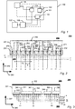
- Fig. 2 shows a schematic drawing of the readout circuitry for a semiconductor radiation detector 200 according to an embodiment of the invention.
- the radiation detector 200 is shown in a cross-section along a first axis 280 and a third axis 282.
- the radiation detector 200 comprises a converter element 201 for converting incident X-ray and / or gamma-ray photons into electron-hole pairs.
- the converter element 201 comprises a first side 208 and a second side 209 opposite to the first side 208. On the first side 208 is arranged at least one cathode 202, and on the second side 209 is arranged 12 elongated parallel detector strip electrodes 260-271 and 37 elongated parallel drift strip electrodes.
- the detector strip electrodes 260-271 and the drift strip electrodes are both extending along a second axis being perpendicular to the first axis 280 and the third axis 282.
- the readout circuitry comprises 16 readout channels, one unique readout channel A1-A12 for each detector strip electrodes 260-271, and one common readout channel D1-D4 for each of four groups of drift strip electrodes.
- the first group of drift strip electrodes being provided with the readout channel D1 comprises four subgroups of drift strip electrodes 253 244 248 252, wherein a subgroup is defined as the drift strip electrodes of the particular group of drift strip electrodes that have the same two neighbouring detector strip electrodes.
- the second group of drift strip electrodes being provided with the readout channel D2 comprises three subgroups 241 245 249
- the third group of drift strip electrodes being provided with the readout channel D3 comprises three subgroups 242 246 250
- the fourth group of drift strip electrodes being provided with the readout channel D4 comprises three subgroups 243 247 251.
- All subgroups 241-251 comprises each three drift strip electrodes, except the two end subgroups 253 252 that each comprises 2 drift strip electrodes.
- the pitch (P2) between the subgroups in this embodiment is four times larger than the pitch (P1) between the detector strip electrodes 260-271.
- the processing unit may detect an event and make a first estimate of the location of the event along the first axis 280 with a first spatial resolution by processing signals obtained from the detector strip electrodes A1-A12, where the first estimate is the location of the specific detector strip electrode being closest to the event.
- the first estimate is the location of the specific detector strip electrode being closest to the event.
- the resolution of the first estimate is given by the pitch (P).
- the specific readout channel of the four readout channels D1-D4 which read out the signal from the subgroup of drift strip electrodes positioned on the left side of the specific detector strip electrode, may be found.
- the specific readout channel of the four readout channels D1-D4, which readout the signal from the subgroup of drift strip electrodes positioned on the right side of the specific detector strip electrode may be found.
- the readout channel D4 read out the signal from the subgroup of drift strip electrodes 247 positioned on the left side of the detector strip electrode 267
- the readout channel D1 read out the signal from the subgroup of drift strip electrodes 248 positioned on the right side of the detector strip electrode 266.
- the first estimate of the location of the event, and the signals readout from the subgroup of drift strip electrodes positioned on the right side and left side of the specific detector strip electrode, may be used to make a second estimate of the location of the event along the first axis, wherein the second estimate has a spatial resolution being higher than the first estimate.
- X int X trg + C * D R ⁇ D L / D R + D L
- X int is the second estimate
- X trg is the first estimate (the location of the specific detector strip electrode)
- D R is a value derived from a signal readout from the subgroup of drift strip electrodes positioned on the right side of the specific detector strip electrode
- D L is a value derived from a signal readout from the subgroup of drift strip electrodes positioned on the left side of the specific detector strip electrode
- C is a calibration constant determined by calibrating the radiation detector.
- the calibration constant C may be selected dependent on a previous estimated location of the event along the third axis 282, i.e. there may be plurality of calibration constants determined by calibration of the radiation detector.
- D R will be a value derived from a signal readout from the readout channel D1 and D L will be a value derived from a signal readout from the readout channel D4.
- D R , and D L may each be a summation of two components, a first component being a maximum value (786 see Fig. 7 ), and a second component being an absolute of the minimum value (787 see Fig. 7 ) of the respective drift signals.
- Each drift strip electrode is preferably provided with an amount of bias being dependent on the distance to the nearest detector strip electrode.
- the central drift strip electrode in each subgroup of drift strip electrodes 241-253 is preferably provided with an electrical potential being more negative than the electrical potential of the two de-central drift strip electrodes. This improves the focusing / steering of the electrons.
- Fig. 3 shows a schematic drawing of the electrical circuit connecting the drift strip electrodes to a voltage divider for a semiconductor radiation detector 300 according to an embodiment of the invention.
- the radiation detector 300 is shown in a cross-section along a first axis 380 and a third axis 382. Only the outer left part and outer right part of the radiation detector is shown.
- the radiation detector 300 comprises a converter element 301 for converting incident X-ray and / or gamma-ray photons into electron-hole pairs.
- the converter element 301 comprises a first side 308 and a second side 309 opposite to the first side 308.
- On the first side 308 at least one cathode 302 is arranged, and on the second side 309 N elongated parallel detector strip electrodes 360 361 369 and N+1 subgroups of drift strip electrodes 431-438 are arranged.
- the radiation detector is of the same type as the radiation detector shown in Fig. 3 , with the difference that each subgroup of drift strip electrodes 341 342 344 comprises seven drift strip electrodes, except the two end subgroups 353 352 that each comprises four drift strip electrodes.
- the voltage source is provided with a voltage divider, whereby four bias potentials V1, V2, V3, and V4 are provided to the drift strip electrodes.
- the potential V1 is most negative relative to the potential of the detector strip electrodes 360 361 369
- the potential V2 is second most negative
- the potential V3 is third most negative
- the potential V4 is least negative relative to the potential of the detector strip electrodes 360 361 369.
- the amount of bias provided to each drift electrodes is dependent on the distance from the drift strip electrode to the nearest detector strip electrode.
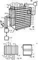
- Fig. 4 shows a schematic drawing of a 3D semiconductor radiation detector according to an embodiment of the invention.
- Fig. 4a shows a perspective view
- Fig. 4b shows a close-up of the area 487 shown in Fig. 4a
- Fig. 4c shows a close-up of the area 488 shown in Fig. 4a .
- the radiation detector 400 comprises a converter element 401 for converting incident X-ray and / or gamma-ray photons into electron-hole pairs (to ease the understanding, the converter element 401 is made transparent in Fig. 4a ).
- the converter element 401 comprises a first side 408 and a second side 409 opposite to the first side 408.
- the cathode strips 420 429 each have a length (L3) and a width (W3)
- the detector strip electrodes 460-469 each have a length (L1) and a width (W1)
- the drift strip electrodes 431-438 each have a length (L2) and a width (W2).
- the detector strip electrodes 460-469 and the drift strip electrodes 431-438 are both extending along a second axis 481, and the cathode strips 420-429 are extending along a first axis 480 being perpendicular to the second axis 481.
- the cathode strip electrodes 420-429 and the drift strip electrodes 431-438 are both connected to a voltage source 405.
- the voltage source 405 is configured to provide the cathode strips 431-438 with a potential being negative relative to the potential of both the drift strip electrodes 431-438 and the detector strip electrodes 460-469, whereby holes are "propagating" towards the cathode strip electrodes 420-429 and electrons are propagating toward the detector strip electrodes 460-469.
- the voltage source 405 is further configured to provide the drift strip electrodes 431-438 with a potential being negative relative to the potential of the detector strip electrodes 460-469, whereby the electrons are focused towards the detector strip electrodes 460-469.
- the radiation detector 400 further comprises a readout circuitry 406 being configured to read out signals from the detector strip electrodes 460-469, the drift strip electrodes 431-438, and the cathode strip electrodes 420-429.
- the readout circuitry 406 is connected to a processing unit 407.
- the processing unit 407 is configured to detect an event within the convert element 401 (the interaction between a X-ray or gamma-ray photon and an electron in the converter element creating an electron / hole pair), and estimate the location of the event in three dimensions.
- the processing unit 407 is configured to estimate the location along the first axis 480 by processing signals obtained from both the detector strip electrodes 460-469 and the drift strip electrodes 431-438, the location along the second axis 481 by processing signals obtained from the cathode strip electrodes 420-429, and the location along a third axis 482 being perpendicular to the first axis 480 and the second axis 481 by processing signals obtained from both the detector strip electrodes 460-469 and the cathode strip electrodes 420-429.
- Fig. 5 shows a flow chart of a method 500 for, along a first axis, estimating a location of an interaction between an X-ray or a gamma-ray photon and a converter element according to an embodiment of the invention.
- the converter element converts incident X-ray and gamma-ray photons into electron-hole pairs, and comprises a first side and a second side, the second side being opposite to the first side.
- signals are received in a processing unit from a plurality of detector electrodes arranged on the second side of the converter element with a pitch (P) along the first axis.
- signals are received in the processing unit from a plurality of drift electrodes also arranged on the second side of said converter element, each drift electrode being connected to a voltage source that applies a potential being negative relative to the electrical potential of the plurality of detector electrodes, whereby electrons are steered towards said plurality of detector electrodes.
- an event in the converter element is determined and the location of the event along the first axis by processing, using the processing unit, the signals received from the plurality of detector electrodes and the plurality of drift electrodes, the location of the event along said first axis is estimated with a precision being greater than the pitch (P).
- Fig. 6 shows a schematic drawing of an electrical circuitry connecting drift strip electrodes to a readout circuitry and a voltage source, according to an embodiment of the present invention.
- the detector 600 may be of similar type as the detector 200 shown in Fig. 2 .
- each subgroup of drift strip electrodes 647 648 comprises 3 drift strip electrodes.
- the drift strip electrodes are provided with a bias potential by the voltage source 605.
- the voltage source 605 is configured to provide the central drift strip electrode for each subgroup 647 648 with a bias potential being more negative relative to the potential provided to the two de-central drift strip electrodes.
- the subgroup 647 is provided with a common readout channel DL and the subgroup 648 is provided with a common readout channel DR.
- Each drift strip electrode is connected to its common readout channel through an electrical connection network comprising a capacitor.
- the electrical connection networks are configured to prevent short circuits between drift strip electrodes provided with different bias potentials.
- Fig. 7 shows a typical drift strip signal 785 detectable (behind a capacitor) at a subgroup of drift strip electrodes, after an event has occurred.
- the signal shows the electrical potential of a subgroup of drift strip electrodes relative to a reference potential over time.
- the first axis 788 is a time axis and the second axis 789 is a potential axis.
- the first peak 790 comes as a result of the movement of the electrons generated by the event, and the negative plateau comes as a result of hole trapping effects in the converter element.
- Both the maximum value 786 and the minimum value 787 may be used to estimate the location of the event.
- the drift strip signals are transient signals induced by the movement of the electrons from the location of an event to the detector strip electrode where they are collected.
Landscapes
- Physics & Mathematics (AREA)
- General Physics & Mathematics (AREA)
- Health & Medical Sciences (AREA)
- High Energy & Nuclear Physics (AREA)
- Spectroscopy & Molecular Physics (AREA)
- Molecular Biology (AREA)
- Life Sciences & Earth Sciences (AREA)
- Engineering & Computer Science (AREA)
- Remote Sensing (AREA)
- Astronomy & Astrophysics (AREA)
- Aviation & Aerospace Engineering (AREA)
- Biomedical Technology (AREA)
- General Health & Medical Sciences (AREA)
- Medical Informatics (AREA)
- Nuclear Medicine, Radiotherapy & Molecular Imaging (AREA)
- Optics & Photonics (AREA)
- Measurement Of Radiation (AREA)
- Nuclear Medicine (AREA)
Claims (14)
- Halbleiterstrahlungsdetektor (100) zum Detektieren von Röntgen- und/oder Gammastrahlung, der Folgendes umfasst:ein Umwandlerelement (101) zum Umwandeln von einfallenden Röntgen- oder Gammaphotonen in Elektron-Loch-Paare, wobei das Umwandlerelement eine erste Seite und eine zweite Seite umfasst, wobei die zweite Seite der ersten Seite gegenüberliegt;wenigstens eine Kathode (102), die auf der ersten Seite des Umwandlerelements angeordnet ist;mehrere Detektorelektroden (103), die auf der zweiten Seite des Umwandlerelements mit einem Rastermaß (P:Pitch) entlang einer ersten Achse angeordnet sind;mehrere Driftelektroden (104), die auf der zweiten Seite des Umwandlerelements angeordnet sind, wobei jede Driftelektrode mit einer Spannungsquelle (105) verbunden ist, die zum Anlegen eines Potentials konfiguriert ist, das relativ zu dem elektrischen Potential der mehreren Detektorelektroden negativ ist, wobei Elektronen zu den mehreren Detektorelektroden hin gelenkt werden;eine Ausleseschaltungsanordnung (106), die zum Auslesen von Signalen von den mehreren Detektorelektroden konfiguriert ist;eine Verarbeitungseinheit (107), die mit der Ausleseschaltungsanordnung verbunden ist, wobei die Verarbeitungseinheit zum Detektieren eines Ereignisses in dem Umwandlerelement konfiguriert ist;wobei die Ausleseschaltungsanordnung ferner zum Auslesen von Signalen von den mehreren Driftelektroden konfiguriert ist, dadurch gekennzeichnet, dass die Verarbeitungseinheit ferner zum Schätzen einer Position des Ereignisses entlang der ersten Achse durch Verarbeiten von Signalen, die von sowohl den Detektorelektroden als auch den Driftelektroden erhalten werden, konfiguriert ist, wobei die Position des Ereignisses entlang der ersten Achse mit einer Genauigkeit größer als das Rastermaß (P) geschätzt wird.
- Halbleiterstrahlungsdetektor nach Anspruch 1, wobei die mehreren Detektorelektroden längliche parallele Detektorstreifenelektroden mit einer Breite (W1) und einer Länge (L1) sind, die sich entlang einer zweiten Achse senkrecht zu der ersten Achse erstrecken, wobei das Rastermaß (P) der Abstand zwischen zwei benachbarten Streifen ist;
wobei die mehreren Driftelektroden längliche parallele Streifenelektroden mit einer Breite (W2) und einer Länge (L2) sind; und
wobei wenigstens eine Driftstreifenelektrode zwischen beliebigen zwei benachbarten Detektorstreifenelektroden angeordnet ist. - Halbleiterstrahlungsdetektor nach Anspruch 2, wobei die Verarbeitungseinheit zum Vornehemen einer ersten Schätzung der Position des Ereignisses entlang der ersten Achse mit einer räumlichen Auflösung durch Verarbeiten von Signalen, die von den Detektorstreifenelektroden erhalten werden, und einer zweiten Schätzung der Position des Ereignisses entlang der ersten Achse mit einer zweiten räumlichen Auflösung, die höher als die erste räumliche Auflösung ist, durch zusätzliches Verarbeiten von Signalen, die von den Driftstreifenelektroden erhalten werden, konfiguriert ist.
- Halbleiterstrahlungsdetektor nach Anspruch 3, wobei die Verarbeitungseinheit zum Erzeugen der zweiten Schätzung der Position des Ereignisses unter Verwendung folgender Gleichung konfiguriert ist:

- Halbleiterstrahlungsdetektor nach einen der Ansprüche 2 bis 4, wobei jede Detektorstreifenelektrode mit einem eindeutigen Auslesekanal von der Ausleseschaltungsanordnung bereitgestellt ist;
wobei die mehreren Driftstreifenelektroden in mehrere Gruppen von Driftstreifenelektroden gruppiert sind, wobei jede Gruppe wenigstens zwei Driftstreifenelektroden umfasst; und
wobei jede Gruppe von Driftstreifenelektroden mit einem gemeinsamen Auslesekanal von der Ausleseschaltungsanordnung bereitgestellt ist. - Halbleiterstrahlungsdetektor nach Anspruch 5, wobei jede bestimmte Gruppe von Driftstreifenelektroden Folgendes umfasst:wenigstens zwei Teilgruppen einer/von Driftstreifenelektrode(n), wobei eine Teilgruppe als die Driftstreifenelektrode(n) der bestimmten Gruppe von Driftstreifenelektroden definiert ist, die dieselben zwei benachbarten Detektorstreifenelektroden aufweist/aufweisen, wobei das Rastermaß (P2) zwischen den Teilgruppen für alle Gruppen der Driftstreifenelektroden wenigstens zweimal das Rastermaß (P) zwischen den Detektorstreifenelektroden ist.
- Halbleiterstrahlungsdetektor nach Anspruch 6, wobei das Rastermaß (P2) zwischen den Teilgruppen für alle Gruppen von Driftstreifenelektroden wenigstens viermal das Rastermaß (P) zwischen den Detektorstreifenelektroden ist.
- Halbleiterstrahlungsdetektor nach einem der Ansprüche 2 bis 7, wobei mehrere längliche parallele Kathodenstreifen auf der ersten Seite des Umwandlerelements angeordnet sind, welche sich entlang der ersten Achse erstrecken, wobei die parallelen Kathodenstreifen eine Breite (W3) und eine Länge (L3) aufweisen und entlang der zweiten Achse mit einem Rastermaß (P3) angeordnet sind;
wobei die Ausleseschaltungsanordnung ferner zum Auslesen von Signalen von den mehreren Kathodenstreifen konfiguriert ist; und
wobei die Verarbeitungseinheit ferner zum Schätzen einer Position des Ereignisses entlang der zweiten Achse durch Verarbeiten von Signalen, die von den mehreren Kathodenstreifen erhalten werden, konfiguriert ist. - Halbleiterstrahlungsdetektor nach einem der Ansprüche 2 bis 8, wobei die Verarbeitungseinheit ferner zum Schätzen der Tiefe des Ereignisses durch Verarbeiten von einem oder mehreren Signalen, die von den Detektorstreifenelektroden erhalten werden, zusammen mit einem oder mehreren Signalen, die von den Kathodenstreifen erhalten werden, konfiguriert ist.
- Verfahren (500) zum Schätzen einer Position einer Interaktion zwischen einem Röntgen- oder Gammaphoton und einem Umwandlerelement entlang einer ersten Achse, wobei das Umwandlerelement einfallende Röntgen- und Gammaphotonen in Elektron-Loch-Paare umwandelt, wobei das Umwandlerelement eine erste Seite und eine zweite Seite umfasst, wobei die zweite Seite der ersten Seite gegenüberliegt; wobei wenigstens eine Kathode auf der ersten Seite des Umwandlerelements angeordnet ist, wobei das Verfahren die folgenden Schritte umfasst:(501) Empfangen von Signalen in einer Verarbeitungseinheit von mehreren Detektorelektroden, die auf der zweiten Seite des Umwandlerelements mit einem Rastermaß (P) entlang der ersten Achse angeordnet sind;(502) Empfangen von Signalen in der Verarbeitungseinheit von mehreren Driftelektroden, die auf der zweiten Seite des Umwandlerelements angeordnet sind, wobei jede Driftelektrode mit einer Spannungsquelle verbunden ist, die ein Potential anlegt, das relativ zu dem elektrischen Potential der mehreren Detektorelektroden negativ ist, wobei Elektronen zu den mehreren Detektorelektroden hin gelenkt werden;(503) Bestimmen eines Ereignisses in dem Wandlerelement unter Verwendung der Verarbeitungseinheit und Schätzen der Position des Ereignisses entlang der ersten Achse durch Verarbeiten der Signale, die von den mehreren Detektorelektroden und den mehreren Driftelektroden erhalten werden, wobei die Position des Ereignisses entlang der ersten Achse mit einer Genauigkeit größer als das Rastermaß (P) geschätzt wird.
- Verfahren nach Anspruch 10, wobei die mehreren Detektorelektroden längliche parallele Detektorstreifenelektroden mit einer Breite (W1) und einer Länge (L1) sind, wobei das Rastermaß (P) der Abstand zwischen zwei benachbarten Streifen ist;
wobei die mehreren Driftelektroden längliche parallele Streifenelektroden mit einer Breite (W2) und einer Länge (L2) sind; und
wobei wenigstens eine Driftstreifenelektrode zwischen beliebigen zwei benachbarten Detektorstreifenelektroden angeordnet ist. - Verfahren nach Anspruch 11, wobei eine erste Schätzung der Position des Ereignisses in der ersten Dimension durch Verarbeiten von Signalen vorgenommen wird, die von den Detektorstreifenelektroden erhalten werden, wobei die erste Schätzung eine erste räumliche Auflösung aufweist; und
wobei eine zweite Schätzung der Position des Ereignisses in der ersten Dimension durch zusätzliches Verarbeiten von Signalen vorgenommen wird, die von den Driftstreifenelektroden erhalten werden, wobei die zweite Schätzung eine zweite räumliche Auflösung aufweist, die höher als die erste räumliche Auflösung ist. - Verfahren nach Anspruch 12, wobei die zweite Schätzung der Position des Ereignisses unter Verwendung folgender Gleichung bestimmt wird:

- Verwendung eines Strahlungsdetektors nach einem der Ansprüche 1 bis 9 in Folgendem:einer medizinischen Bildgebungsvorrichtung, wie etwa einem CT-Scanner, einem PET-Scanner, einem PET-CT-Scanner oder einem SPECT-Scanner;einem Satelliten; odereinem Sicherheitssystem zum Detektieren und Lokalisieren von radioaktivem Material.
Priority Applications (1)
| Application Number | Priority Date | Filing Date | Title |
|---|---|---|---|
| EP14802681.8A EP3074792B1 (de) | 2013-11-26 | 2014-11-26 | Röntgen- und gammastrahlendetektor |
Applications Claiming Priority (3)
| Application Number | Priority Date | Filing Date | Title |
|---|---|---|---|
| EP13194445.6A EP2876465A1 (de) | 2013-11-26 | 2013-11-26 | Röntgen- und Gammastrahlendetektor |
| PCT/EP2014/075643 WO2015078902A1 (en) | 2013-11-26 | 2014-11-26 | X-ray and gamma-ray radiation detector |
| EP14802681.8A EP3074792B1 (de) | 2013-11-26 | 2014-11-26 | Röntgen- und gammastrahlendetektor |
Publications (2)
| Publication Number | Publication Date |
|---|---|
| EP3074792A1 EP3074792A1 (de) | 2016-10-05 |
| EP3074792B1 true EP3074792B1 (de) | 2017-10-11 |
Family
ID=49639790
Family Applications (2)
| Application Number | Title | Priority Date | Filing Date |
|---|---|---|---|
| EP13194445.6A Withdrawn EP2876465A1 (de) | 2013-11-26 | 2013-11-26 | Röntgen- und Gammastrahlendetektor |
| EP14802681.8A Active EP3074792B1 (de) | 2013-11-26 | 2014-11-26 | Röntgen- und gammastrahlendetektor |
Family Applications Before (1)
| Application Number | Title | Priority Date | Filing Date |
|---|---|---|---|
| EP13194445.6A Withdrawn EP2876465A1 (de) | 2013-11-26 | 2013-11-26 | Röntgen- und Gammastrahlendetektor |
Country Status (3)
| Country | Link |
|---|---|
| US (1) | US9921315B2 (de) |
| EP (2) | EP2876465A1 (de) |
| WO (1) | WO2015078902A1 (de) |
Families Citing this family (6)
| Publication number | Priority date | Publication date | Assignee | Title |
|---|---|---|---|---|
| EP3232229A1 (de) * | 2016-04-13 | 2017-10-18 | Nokia Technologies Oy | Vorrichtung zur erfassung von strahlung |
| CN106249270B (zh) * | 2016-08-31 | 2023-04-25 | 同方威视技术股份有限公司 | 半导体探测器 |
| EP3306353A1 (de) | 2016-10-07 | 2018-04-11 | Danmarks Tekniske Universitet | Strahlungsdetektor |
| EP4544326A1 (de) | 2022-06-27 | 2025-04-30 | Danmarks Tekniske Universitet | Halbleiterstrahlungssensorvorrichtung und verfahren zum trainieren eines künstlichen neuronalen netzwerks zur signalverarbeitung |
| CN116755132A (zh) * | 2023-06-26 | 2023-09-15 | 中广核工程有限公司 | 一种双能x射线探测器结构及探测方法 |
| CN117969604B (zh) * | 2024-04-02 | 2024-06-28 | 中国科学技术大学 | 低物质量圆柱形微结构气体探测器及其制备方法 |
Family Cites Families (13)
| Publication number | Priority date | Publication date | Assignee | Title |
|---|---|---|---|---|
| US6362484B1 (en) * | 1995-07-14 | 2002-03-26 | Imec Vzw | Imager or particle or radiation detector and method of manufacturing the same |
| US6121622A (en) * | 1995-07-14 | 2000-09-19 | Yeda Research And Development Co., Ltd. | Imager or particle detector and method of manufacturing the same |
| US6046454A (en) * | 1995-10-13 | 2000-04-04 | Digirad Corporation | Semiconductor radiation detector with enhanced charge collection |
| US6037595A (en) * | 1995-10-13 | 2000-03-14 | Digirad Corporation | Radiation detector with shielding electrode |
| IL137579A (en) * | 2000-07-30 | 2006-12-31 | Orbotech Medical Solutions Ltd | Gamma-ray detector for coincidence detection |
| IL145745A (en) * | 2001-10-03 | 2006-08-20 | Orbotech Medical Solutions Ltd | Two-dimensional radiation detector |
| US8067744B2 (en) * | 2005-07-06 | 2011-11-29 | Ge Healthcare Israel | Method and apparatus of detecting ionizing radiation |
| JP5371086B2 (ja) * | 2008-10-29 | 2013-12-18 | 独立行政法人理化学研究所 | 半導体放射線検出装置 |
| US20100252744A1 (en) | 2009-04-06 | 2010-10-07 | Koninklijke Philips Electronics N.V. | Radiation detector with a plurality of electrode systems |
| RU2567436C2 (ru) * | 2010-09-13 | 2015-11-10 | Конинклейке Филипс Электроникс Н.В. | Детектор излучения с направляющими электродами |
| EP2649470B1 (de) * | 2010-12-07 | 2017-09-27 | Koninklijke Philips N.V. | Röntgendetektor mit direktumwandung |
| BR112014014064A8 (pt) * | 2011-12-13 | 2017-06-13 | Koninklijke Philips Nv | detector de radiação e aparelho detector de radiação |
| US20130161523A1 (en) * | 2011-12-23 | 2013-06-27 | General Electric Company | Radiation detector with voltage-biased focus grid |
-
2013
- 2013-11-26 EP EP13194445.6A patent/EP2876465A1/de not_active Withdrawn
-
2014
- 2014-11-26 US US15/039,448 patent/US9921315B2/en active Active
- 2014-11-26 WO PCT/EP2014/075643 patent/WO2015078902A1/en not_active Ceased
- 2014-11-26 EP EP14802681.8A patent/EP3074792B1/de active Active
Non-Patent Citations (1)
| Title |
|---|
| None * |
Also Published As
| Publication number | Publication date |
|---|---|
| US20170168168A1 (en) | 2017-06-15 |
| EP2876465A1 (de) | 2015-05-27 |
| EP3074792A1 (de) | 2016-10-05 |
| US9921315B2 (en) | 2018-03-20 |
| WO2015078902A1 (en) | 2015-06-04 |
Similar Documents
| Publication | Publication Date | Title |
|---|---|---|
| EP3074792B1 (de) | Röntgen- und gammastrahlendetektor | |
| JP7317586B2 (ja) | 医用画像処理装置、方法及びプログラム | |
| US9835739B2 (en) | Method and apparatus for processing signals of semiconductor detector | |
| EP1840597A2 (de) | Energiekalibrierverfahren und Vorrichtung zur Strahlungsdetektion und radiologischen Bildgebung | |
| US7734017B2 (en) | Anti-scatter-grid for a radiation detector | |
| US10679762B2 (en) | Analyzing grid for phase contrast imaging and/or dark-field imaging | |
| Jeong et al. | Comparison between pixelated scintillators: CsI (Tl), LaCl 3 (Ce) and LYSO (Ce) when coupled to a silicon photomultipliers array | |
| JP5427655B2 (ja) | 放射線計測装置,核医学診断装置 | |
| US20080157255A1 (en) | Semiconductor radiation detector and radiation detection equipment | |
| RU2567436C2 (ru) | Детектор излучения с направляющими электродами | |
| Yin et al. | 3-D spatial resolution of 350/spl mu/m pitch pixelated CdZnTe detectors for imaging applications | |
| Akamatsu et al. | Evaluation of a Hamamatsu TOF-PET detector module with 3.2-mm pitch LFS scintillators and a 256-channel SiPM array | |
| Li et al. | DOI correction for gamma ray energy reconstruction based on energy segment in 3D position-sensitive CdZnTe detectors | |
| US6884982B2 (en) | Methods and apparatus for improving resolution and reducing the effects of signal coupling in an electronic imager | |
| Poladyan et al. | Gain invariant coordinate reconstruction for SiPM-Based pixelated gamma detectors with multiplexed readout | |
| EP3523678B1 (de) | Halbleiterdetektor mit segmentierter kathode | |
| Li et al. | Feasible energy calibration for multi-threshold photon-counting detectors based on reconstructed XRF spectra | |
| JPH02147883A (ja) | 多チャンネル放射線検出装置 | |
| US11526985B1 (en) | Method and apparatus for improving the spatial resolution in molecular breast tomosynthesis | |
| JPH11344568A (ja) | 核医学診断装置 | |
| Vernekohl et al. | Robust detector calibration for a novel PET system based on cross-strip CZT detectors | |
| CN219810870U (zh) | 多层x射线探测器 | |
| Coburn et al. | Results of charge sharing tests in a Ge-strip detector | |
| US20240125947A1 (en) | X-ray scatter estimation | |
| Zhou et al. | A QTC-based signal readout for position-sensitive multi-output detectors |
Legal Events
| Date | Code | Title | Description |
|---|---|---|---|
| PUAI | Public reference made under article 153(3) epc to a published international application that has entered the european phase |
Free format text: ORIGINAL CODE: 0009012 |
|
| 17P | Request for examination filed |
Effective date: 20160623 |
|
| AK | Designated contracting states |
Kind code of ref document: A1 Designated state(s): AL AT BE BG CH CY CZ DE DK EE ES FI FR GB GR HR HU IE IS IT LI LT LU LV MC MK MT NL NO PL PT RO RS SE SI SK SM TR |
|
| AX | Request for extension of the european patent |
Extension state: BA ME |
|
| DAX | Request for extension of the european patent (deleted) | ||
| GRAP | Despatch of communication of intention to grant a patent |
Free format text: ORIGINAL CODE: EPIDOSNIGR1 |
|
| STAA | Information on the status of an ep patent application or granted ep patent |
Free format text: STATUS: GRANT OF PATENT IS INTENDED |
|
| INTG | Intention to grant announced |
Effective date: 20170424 |
|
| GRAS | Grant fee paid |
Free format text: ORIGINAL CODE: EPIDOSNIGR3 |
|
| GRAA | (expected) grant |
Free format text: ORIGINAL CODE: 0009210 |
|
| STAA | Information on the status of an ep patent application or granted ep patent |
Free format text: STATUS: THE PATENT HAS BEEN GRANTED |
|
| AK | Designated contracting states |
Kind code of ref document: B1 Designated state(s): AL AT BE BG CH CY CZ DE DK EE ES FI FR GB GR HR HU IE IS IT LI LT LU LV MC MK MT NL NO PL PT RO RS SE SI SK SM TR |
|
| REG | Reference to a national code |
Ref country code: GB Ref legal event code: FG4D |
|
| REG | Reference to a national code |
Ref country code: CH Ref legal event code: EP |
|
| REG | Reference to a national code |
Ref country code: IE Ref legal event code: FG4D |
|
| REG | Reference to a national code |
Ref country code: AT Ref legal event code: REF Ref document number: 936535 Country of ref document: AT Kind code of ref document: T Effective date: 20171115 |
|
| REG | Reference to a national code |
Ref country code: DE Ref legal event code: R096 Ref document number: 602014015776 Country of ref document: DE |
|
| REG | Reference to a national code |
Ref country code: FR Ref legal event code: PLFP Year of fee payment: 4 |
|
| REG | Reference to a national code |
Ref country code: NL Ref legal event code: MP Effective date: 20171011 |
|
| REG | Reference to a national code |
Ref country code: LT Ref legal event code: MG4D |
|
| REG | Reference to a national code |
Ref country code: AT Ref legal event code: MK05 Ref document number: 936535 Country of ref document: AT Kind code of ref document: T Effective date: 20171011 |
|
| PG25 | Lapsed in a contracting state [announced via postgrant information from national office to epo] |
Ref country code: NL Free format text: LAPSE BECAUSE OF FAILURE TO SUBMIT A TRANSLATION OF THE DESCRIPTION OR TO PAY THE FEE WITHIN THE PRESCRIBED TIME-LIMIT Effective date: 20171011 |
|
| PG25 | Lapsed in a contracting state [announced via postgrant information from national office to epo] |
Ref country code: ES Free format text: LAPSE BECAUSE OF FAILURE TO SUBMIT A TRANSLATION OF THE DESCRIPTION OR TO PAY THE FEE WITHIN THE PRESCRIBED TIME-LIMIT Effective date: 20171011 Ref country code: NO Free format text: LAPSE BECAUSE OF FAILURE TO SUBMIT A TRANSLATION OF THE DESCRIPTION OR TO PAY THE FEE WITHIN THE PRESCRIBED TIME-LIMIT Effective date: 20180111 Ref country code: FI Free format text: LAPSE BECAUSE OF FAILURE TO SUBMIT A TRANSLATION OF THE DESCRIPTION OR TO PAY THE FEE WITHIN THE PRESCRIBED TIME-LIMIT Effective date: 20171011 Ref country code: SE Free format text: LAPSE BECAUSE OF FAILURE TO SUBMIT A TRANSLATION OF THE DESCRIPTION OR TO PAY THE FEE WITHIN THE PRESCRIBED TIME-LIMIT Effective date: 20171011 Ref country code: LT Free format text: LAPSE BECAUSE OF FAILURE TO SUBMIT A TRANSLATION OF THE DESCRIPTION OR TO PAY THE FEE WITHIN THE PRESCRIBED TIME-LIMIT Effective date: 20171011 |
|
| PG25 | Lapsed in a contracting state [announced via postgrant information from national office to epo] |
Ref country code: HR Free format text: LAPSE BECAUSE OF FAILURE TO SUBMIT A TRANSLATION OF THE DESCRIPTION OR TO PAY THE FEE WITHIN THE PRESCRIBED TIME-LIMIT Effective date: 20171011 Ref country code: BG Free format text: LAPSE BECAUSE OF FAILURE TO SUBMIT A TRANSLATION OF THE DESCRIPTION OR TO PAY THE FEE WITHIN THE PRESCRIBED TIME-LIMIT Effective date: 20180111 Ref country code: IS Free format text: LAPSE BECAUSE OF FAILURE TO SUBMIT A TRANSLATION OF THE DESCRIPTION OR TO PAY THE FEE WITHIN THE PRESCRIBED TIME-LIMIT Effective date: 20180211 Ref country code: RS Free format text: LAPSE BECAUSE OF FAILURE TO SUBMIT A TRANSLATION OF THE DESCRIPTION OR TO PAY THE FEE WITHIN THE PRESCRIBED TIME-LIMIT Effective date: 20171011 Ref country code: GR Free format text: LAPSE BECAUSE OF FAILURE TO SUBMIT A TRANSLATION OF THE DESCRIPTION OR TO PAY THE FEE WITHIN THE PRESCRIBED TIME-LIMIT Effective date: 20180112 Ref country code: LV Free format text: LAPSE BECAUSE OF FAILURE TO SUBMIT A TRANSLATION OF THE DESCRIPTION OR TO PAY THE FEE WITHIN THE PRESCRIBED TIME-LIMIT Effective date: 20171011 Ref country code: AT Free format text: LAPSE BECAUSE OF FAILURE TO SUBMIT A TRANSLATION OF THE DESCRIPTION OR TO PAY THE FEE WITHIN THE PRESCRIBED TIME-LIMIT Effective date: 20171011 |
|
| REG | Reference to a national code |
Ref country code: DE Ref legal event code: R097 Ref document number: 602014015776 Country of ref document: DE |
|
| PG25 | Lapsed in a contracting state [announced via postgrant information from national office to epo] |
Ref country code: CH Free format text: LAPSE BECAUSE OF NON-PAYMENT OF DUE FEES Effective date: 20171130 Ref country code: EE Free format text: LAPSE BECAUSE OF FAILURE TO SUBMIT A TRANSLATION OF THE DESCRIPTION OR TO PAY THE FEE WITHIN THE PRESCRIBED TIME-LIMIT Effective date: 20171011 Ref country code: DK Free format text: LAPSE BECAUSE OF FAILURE TO SUBMIT A TRANSLATION OF THE DESCRIPTION OR TO PAY THE FEE WITHIN THE PRESCRIBED TIME-LIMIT Effective date: 20171011 Ref country code: SK Free format text: LAPSE BECAUSE OF FAILURE TO SUBMIT A TRANSLATION OF THE DESCRIPTION OR TO PAY THE FEE WITHIN THE PRESCRIBED TIME-LIMIT Effective date: 20171011 Ref country code: MC Free format text: LAPSE BECAUSE OF FAILURE TO SUBMIT A TRANSLATION OF THE DESCRIPTION OR TO PAY THE FEE WITHIN THE PRESCRIBED TIME-LIMIT Effective date: 20171011 Ref country code: CZ Free format text: LAPSE BECAUSE OF FAILURE TO SUBMIT A TRANSLATION OF THE DESCRIPTION OR TO PAY THE FEE WITHIN THE PRESCRIBED TIME-LIMIT Effective date: 20171011 Ref country code: LI Free format text: LAPSE BECAUSE OF NON-PAYMENT OF DUE FEES Effective date: 20171130 |
|
| PLBE | No opposition filed within time limit |
Free format text: ORIGINAL CODE: 0009261 |
|
| STAA | Information on the status of an ep patent application or granted ep patent |
Free format text: STATUS: NO OPPOSITION FILED WITHIN TIME LIMIT |
|
| PG25 | Lapsed in a contracting state [announced via postgrant information from national office to epo] |
Ref country code: PL Free format text: LAPSE BECAUSE OF FAILURE TO SUBMIT A TRANSLATION OF THE DESCRIPTION OR TO PAY THE FEE WITHIN THE PRESCRIBED TIME-LIMIT Effective date: 20171011 Ref country code: IT Free format text: LAPSE BECAUSE OF FAILURE TO SUBMIT A TRANSLATION OF THE DESCRIPTION OR TO PAY THE FEE WITHIN THE PRESCRIBED TIME-LIMIT Effective date: 20171011 Ref country code: RO Free format text: LAPSE BECAUSE OF FAILURE TO SUBMIT A TRANSLATION OF THE DESCRIPTION OR TO PAY THE FEE WITHIN THE PRESCRIBED TIME-LIMIT Effective date: 20171011 Ref country code: LU Free format text: LAPSE BECAUSE OF NON-PAYMENT OF DUE FEES Effective date: 20171126 Ref country code: SM Free format text: LAPSE BECAUSE OF FAILURE TO SUBMIT A TRANSLATION OF THE DESCRIPTION OR TO PAY THE FEE WITHIN THE PRESCRIBED TIME-LIMIT Effective date: 20171011 |
|
| REG | Reference to a national code |
Ref country code: BE Ref legal event code: MM Effective date: 20171130 |
|
| REG | Reference to a national code |
Ref country code: IE Ref legal event code: MM4A |
|
| 26N | No opposition filed |
Effective date: 20180712 |
|
| PG25 | Lapsed in a contracting state [announced via postgrant information from national office to epo] |
Ref country code: MT Free format text: LAPSE BECAUSE OF NON-PAYMENT OF DUE FEES Effective date: 20171126 |
|
| PG25 | Lapsed in a contracting state [announced via postgrant information from national office to epo] |
Ref country code: IE Free format text: LAPSE BECAUSE OF NON-PAYMENT OF DUE FEES Effective date: 20171126 |
|
| PG25 | Lapsed in a contracting state [announced via postgrant information from national office to epo] |
Ref country code: SI Free format text: LAPSE BECAUSE OF FAILURE TO SUBMIT A TRANSLATION OF THE DESCRIPTION OR TO PAY THE FEE WITHIN THE PRESCRIBED TIME-LIMIT Effective date: 20171011 Ref country code: BE Free format text: LAPSE BECAUSE OF NON-PAYMENT OF DUE FEES Effective date: 20171130 |
|
| PG25 | Lapsed in a contracting state [announced via postgrant information from national office to epo] |
Ref country code: HU Free format text: LAPSE BECAUSE OF FAILURE TO SUBMIT A TRANSLATION OF THE DESCRIPTION OR TO PAY THE FEE WITHIN THE PRESCRIBED TIME-LIMIT; INVALID AB INITIO Effective date: 20141126 |
|
| PG25 | Lapsed in a contracting state [announced via postgrant information from national office to epo] |
Ref country code: CY Free format text: LAPSE BECAUSE OF FAILURE TO SUBMIT A TRANSLATION OF THE DESCRIPTION OR TO PAY THE FEE WITHIN THE PRESCRIBED TIME-LIMIT Effective date: 20171011 |
|
| PG25 | Lapsed in a contracting state [announced via postgrant information from national office to epo] |
Ref country code: MK Free format text: LAPSE BECAUSE OF FAILURE TO SUBMIT A TRANSLATION OF THE DESCRIPTION OR TO PAY THE FEE WITHIN THE PRESCRIBED TIME-LIMIT Effective date: 20171011 |
|
| PG25 | Lapsed in a contracting state [announced via postgrant information from national office to epo] |
Ref country code: TR Free format text: LAPSE BECAUSE OF FAILURE TO SUBMIT A TRANSLATION OF THE DESCRIPTION OR TO PAY THE FEE WITHIN THE PRESCRIBED TIME-LIMIT Effective date: 20171011 |
|
| PG25 | Lapsed in a contracting state [announced via postgrant information from national office to epo] |
Ref country code: PT Free format text: LAPSE BECAUSE OF FAILURE TO SUBMIT A TRANSLATION OF THE DESCRIPTION OR TO PAY THE FEE WITHIN THE PRESCRIBED TIME-LIMIT Effective date: 20171011 |
|
| PG25 | Lapsed in a contracting state [announced via postgrant information from national office to epo] |
Ref country code: AL Free format text: LAPSE BECAUSE OF FAILURE TO SUBMIT A TRANSLATION OF THE DESCRIPTION OR TO PAY THE FEE WITHIN THE PRESCRIBED TIME-LIMIT Effective date: 20171011 |
|
| P01 | Opt-out of the competence of the unified patent court (upc) registered |
Effective date: 20230421 |
|
| PGFP | Annual fee paid to national office [announced via postgrant information from national office to epo] |
Ref country code: FR Payment date: 20250930 Year of fee payment: 12 |
|
| PGFP | Annual fee paid to national office [announced via postgrant information from national office to epo] |
Ref country code: DE Payment date: 20250930 Year of fee payment: 12 |
|
| PGFP | Annual fee paid to national office [announced via postgrant information from national office to epo] |
Ref country code: GB Payment date: 20251001 Year of fee payment: 12 |