EP3073573A1 - Method for manufacturing coil antenna and method for manufacturing coil antenna mounting body - Google Patents
Method for manufacturing coil antenna and method for manufacturing coil antenna mounting body Download PDFInfo
- Publication number
- EP3073573A1 EP3073573A1 EP14861998.4A EP14861998A EP3073573A1 EP 3073573 A1 EP3073573 A1 EP 3073573A1 EP 14861998 A EP14861998 A EP 14861998A EP 3073573 A1 EP3073573 A1 EP 3073573A1
- Authority
- EP
- European Patent Office
- Prior art keywords
- coil antenna
- coil
- mounting base
- antenna body
- wire
- Prior art date
- Legal status (The legal status is an assumption and is not a legal conclusion. Google has not performed a legal analysis and makes no representation as to the accuracy of the status listed.)
- Withdrawn
Links
- 238000004519 manufacturing process Methods 0.000 title claims abstract description 36
- 238000000034 method Methods 0.000 title claims description 19
- 239000000696 magnetic material Substances 0.000 claims abstract description 34
- 229910000679 solder Inorganic materials 0.000 claims description 11
- 238000005304 joining Methods 0.000 claims description 7
- 239000000853 adhesive Substances 0.000 description 8
- 230000008569 process Effects 0.000 description 8
- 238000010586 diagram Methods 0.000 description 7
- 229910000859 α-Fe Inorganic materials 0.000 description 7
- 230000001070 adhesive effect Effects 0.000 description 6
- 239000011347 resin Substances 0.000 description 5
- 229920005989 resin Polymers 0.000 description 5
- 238000004891 communication Methods 0.000 description 4
- RYGMFSIKBFXOCR-UHFFFAOYSA-N Copper Chemical compound [Cu] RYGMFSIKBFXOCR-UHFFFAOYSA-N 0.000 description 3
- 238000005476 soldering Methods 0.000 description 3
- XEEYBQQBJWHFJM-UHFFFAOYSA-N Iron Chemical compound [Fe] XEEYBQQBJWHFJM-UHFFFAOYSA-N 0.000 description 2
- PXHVJJICTQNCMI-UHFFFAOYSA-N Nickel Chemical compound [Ni] PXHVJJICTQNCMI-UHFFFAOYSA-N 0.000 description 2
- 239000000463 material Substances 0.000 description 2
- 238000002203 pretreatment Methods 0.000 description 2
- 230000004044 response Effects 0.000 description 2
- 230000035939 shock Effects 0.000 description 2
- 238000003466 welding Methods 0.000 description 2
- 239000004642 Polyimide Substances 0.000 description 1
- 229910045601 alloy Inorganic materials 0.000 description 1
- 239000000956 alloy Substances 0.000 description 1
- 230000004075 alteration Effects 0.000 description 1
- 230000008901 benefit Effects 0.000 description 1
- 239000011230 binding agent Substances 0.000 description 1
- 230000015572 biosynthetic process Effects 0.000 description 1
- 230000001413 cellular effect Effects 0.000 description 1
- 239000010941 cobalt Substances 0.000 description 1
- 229910017052 cobalt Inorganic materials 0.000 description 1
- GUTLYIVDDKVIGB-UHFFFAOYSA-N cobalt atom Chemical compound [Co] GUTLYIVDDKVIGB-UHFFFAOYSA-N 0.000 description 1
- 229910052802 copper Inorganic materials 0.000 description 1
- 239000010949 copper Substances 0.000 description 1
- 238000005520 cutting process Methods 0.000 description 1
- 238000009792 diffusion process Methods 0.000 description 1
- 230000000694 effects Effects 0.000 description 1
- 239000010408 film Substances 0.000 description 1
- 238000010304 firing Methods 0.000 description 1
- 238000010348 incorporation Methods 0.000 description 1
- 229910052742 iron Inorganic materials 0.000 description 1
- 229910052759 nickel Inorganic materials 0.000 description 1
- 230000008520 organization Effects 0.000 description 1
- 230000035699 permeability Effects 0.000 description 1
- 229920001721 polyimide Polymers 0.000 description 1
- 239000000843 powder Substances 0.000 description 1
- 230000009467 reduction Effects 0.000 description 1
- 238000006467 substitution reaction Methods 0.000 description 1
- 239000010409 thin film Substances 0.000 description 1
Images



Classifications
-
- H—ELECTRICITY
- H01—ELECTRIC ELEMENTS
- H01Q—ANTENNAS, i.e. RADIO AERIALS
- H01Q7/00—Loop antennas with a substantially uniform current distribution around the loop and having a directional radiation pattern in a plane perpendicular to the plane of the loop
- H01Q7/06—Loop antennas with a substantially uniform current distribution around the loop and having a directional radiation pattern in a plane perpendicular to the plane of the loop with core of ferromagnetic material
-
- H—ELECTRICITY
- H01—ELECTRIC ELEMENTS
- H01Q—ANTENNAS, i.e. RADIO AERIALS
- H01Q7/00—Loop antennas with a substantially uniform current distribution around the loop and having a directional radiation pattern in a plane perpendicular to the plane of the loop
- H01Q7/06—Loop antennas with a substantially uniform current distribution around the loop and having a directional radiation pattern in a plane perpendicular to the plane of the loop with core of ferromagnetic material
- H01Q7/08—Ferrite rod or like elongated core
-
- H—ELECTRICITY
- H05—ELECTRIC TECHNIQUES NOT OTHERWISE PROVIDED FOR
- H05K—PRINTED CIRCUITS; CASINGS OR CONSTRUCTIONAL DETAILS OF ELECTRIC APPARATUS; MANUFACTURE OF ASSEMBLAGES OF ELECTRICAL COMPONENTS
- H05K13/00—Apparatus or processes specially adapted for manufacturing or adjusting assemblages of electric components
- H05K13/04—Mounting of components, e.g. of leadless components
- H05K13/046—Surface mounting
- H05K13/0465—Surface mounting by soldering
-
- H—ELECTRICITY
- H01—ELECTRIC ELEMENTS
- H01Q—ANTENNAS, i.e. RADIO AERIALS
- H01Q1/00—Details of, or arrangements associated with, antennas
- H01Q1/12—Supports; Mounting means
- H01Q1/22—Supports; Mounting means by structural association with other equipment or articles
- H01Q1/24—Supports; Mounting means by structural association with other equipment or articles with receiving set
- H01Q1/241—Supports; Mounting means by structural association with other equipment or articles with receiving set used in mobile communications, e.g. GSM
- H01Q1/242—Supports; Mounting means by structural association with other equipment or articles with receiving set used in mobile communications, e.g. GSM specially adapted for hand-held use
- H01Q1/243—Supports; Mounting means by structural association with other equipment or articles with receiving set used in mobile communications, e.g. GSM specially adapted for hand-held use with built-in antennas
Definitions
- the present invention relates to methods of manufacturing a coil antenna and methods of manufacturing a coil antenna package.
- Antennas to be mounted on smartphones include loop antennas and spiral antennas. Of these, spiral antennas are believed to increase a communication distance.
- Patent Document 1 and Patent Document 2 listed below disclose a bar-shaped or sheet-shaped magnetic material that holds small pieces of ferrite whose length of each side is a few millimeters in PET resin.
- Patent Document 1 discloses, in response to a demand for antenna flexibility, an antenna core that includes magnetic members each formed of a thin film magnetic material to which resin is applied, a flexible tube that hermetically seals a magnetic core part into which the magnetic members are stacked without being fixed to each other, and an oil solution interposed between the magnetic core part and the flexible tube. It is illustrated that according to this antenna core, it is possible to prevent generation of cracks and damage and to stabilize the shape, so that it is possible to obtain good antenna characteristics.
- Patent Document 2 discloses, in response to demands for shock resistance and a diversity of shapes, an antenna core formed of an insulating soft magnetic material that includes soft magnetic material powder and an organic binder. It is illustrated that as a result of using an insulating soft magnetic material having particular magnetic permeability frequency characteristics, a coil antenna including the antenna core obtains better characteristics than conventional coil antennas and has good shock resistance, processability, and mountability.
- an antenna package formed by connecting the coil antenna to a board also is desired to be kept thin. Furthermore, it is also desired that the antenna package be manufactured at good efficiency.
- Patent Document 1 and Patent Document 2 are silent about a method of treating the terminal ends of a coil wire wound around an antenna core.
- the method of treating the terminal ends of a coil wire is believed to affect process efficiency and also the thickness of an antenna package.
- soldering the terminal ends of a coil wire individually to an electronic board has the problem of making manufacture inefficient and making the reduction of thickness difficult.
- the present invention has an object of providing a method of manufacturing an efficiently mountable coil antenna using a flexible plate-shaped magnetic material as a core while keeping the coil antenna low-profile.
- a method of manufacturing a coil antenna that includes a flexible plate-shaped coil antenna body containing a magnetic material, and a coil wire wound around the coil antenna body in a direction perpendicular to a longitudinal direction of the coil antenna body so as to form a loop, includes the steps of temporarily fixing a terminal end of the coil wire to the coil antenna body and performing treatment on part of the coil wire that comes into contact with a connection part of a mounting base on which the coil antenna is to be mounted, so that the coil antenna is electrically connectable to the mounting base.
- a method of manufacturing a coil antenna package that includes a coil antenna including a flexible plate-shaped coil antenna body containing a magnetic material, and a coil wire wound around the coil antenna body in a direction perpendicular to a longitudinal direction of the coil antenna body so as to form a loop; and a mounting base on which the coil antenna is surface-mounted, the mounting base including a connection part at a position where the mounting base is connected to the coil antenna, includes the steps of temporarily fixing a terminal end of the coil wire to the coil antenna body, performing treatment on part of the coil wire that comes into contact with the connection part of the mounting base, so that the coil antenna is electrically connectable to the mounting base, and disposing the coil antenna on the mounting base so that the part of the coil wire comes into contact with the connection part, and joining the coil antenna to the mounting base with solder flow.
- a method of manufacturing an efficiently mountable coil antenna using a flexible plate-shaped magnetic material as a core while keeping the coil antenna low-profile is provided.
- a method of manufacturing a coil antenna package that suppresses an increase in thickness due to the joining of a coil antenna and a mounting base is provided.
- a method of manufacturing a coil antenna that includes a flexible plate-shaped coil antenna body containing a magnetic material, and a coil wire wound around the coil antenna body in a direction perpendicular to a longitudinal direction of the coil antenna body so as to form a loop includes the steps of temporarily fixing a terminal end of the coil wire to the coil antenna body and performing treatment on part of the coil wire that comes into contact with a connection part of a mounting base on which the coil antenna is to be mounted, so that the coil antenna is electrically connectable to the mounting base.
- a method of manufacturing a coil antenna package that includes a coil antenna including a flexible plate-shaped coil antenna body containing a magnetic material, and a coil wire wound around the coil antenna body in a direction perpendicular to a longitudinal direction of the coil antenna body so as to form a loop; and a mounting base on which the coil antenna is surface-mounted, the mounting base including a connection part at a position where the mounting base is connected to the coil antenna, includes the steps of temporarily fixing a terminal end of the coil wire to the coil antenna body, performing treatment on part of the coil wire that comes into contact with the connection part of the mounting base, so that the coil antenna is electrically connectable to the mounting base, and disposing the coil antenna on the mounting base so that the part of the coil wire comes into contact with the connection part, and joining the coil antenna to the mounting base with solder flow.
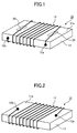
- FIG. 1 and FIG. 2 are perspective views each illustrating the exterior of a coil antenna before the coil antenna is mounted on a mounting base according to a method of manufacturing a coil antenna of a first embodiment.
- a coil antenna 10 includes a flexible plate-shaped coil antenna body 11 containing a magnetic material, and a coil wire 12 wound around the coil antenna body 11 in a transverse direction (a direction perpendicular to a longitudinal direction) of the coil antenna body 11 so as to form a loop.
- a method of manufacturing the coil antenna 10 includes a process of temporarily fixing terminal ends 12a and 12b of the coil wire 12 to the coil antenna body 11 and a process of performing treatment on at least part of the coil wire 12 that comes into contact with a connection part of a mounting base (not illustrated) on which the coil antenna 10 is to be mounted, so that the coil antenna 10 is electrically connectable to the mounting base.
- the terminal ends 12a and 12b of the coil wire 12 of the coil antenna 10 are temporarily fixed to a surface other than a surface 11a of the coil antenna body 11 that faces (connects to) the mounting base when the coil antenna 10 is disposed on the mounting base.
- the coil antenna body 11 includes a surface 11b that is opposite to the surface 11a that faces the mounting base. Furthermore, the coil antenna 10 includes antenna connection pattern contact parts 20 at positions corresponding to connection parts (antenna connection patterns) formed on the mounting base.
- the terminal ends 12a and 12b of the coil wire 12 are temporarily fixed to a surface of the coil antenna body 11 using an adhesive agent or the like.
- the surface to which the terminal ends 12a and 12b are temporarily fixed is preferably a surface of the coil antenna body 11 adjoining the surface 11a that faces (connects to) the mounting base as illustrated in FIG. 1 , in order to minimize an increase in the thickness of the coil antenna 10 after its mounting on the mounting base. If such an arrangement is difficult for structural reasons, however, the surface to which the terminal ends 12a and 12b are temporarily fixed may be the surface 11b opposite to the surface 11a that connects to the mounting base as illustrated in FIG. 2 , on condition that the amount of application of an adhesive agent is minimized.
- pre-treatment is performed on at least parts of the coil wire 12, placed on the surface 11a that connects to the mounting base, which parts are in the antenna connection pattern contact parts 20 at positions corresponding to the antenna connection patterns formed on the mounting base.
- the pre-treatment is performed so as to make the coil antenna 10 and the mounting base easily connectable in a solder flow process, and includes, for example, formation of pre-soldered parts and removal of coats of coated copper wires.
- the coil antenna body 11 may be a flexible plate-shaped body containing a magnetic material.
- magnetic materials include ferrite, iron, nickel, cobalt, and their alloys, among which ferrite is preferable.
- the coil wire 12 for example, a copper wire, preferably, a coated copper wire, may be used.
- FIG. 3 and FIG. 4 are plan views of a coil antenna before mounting the coil antenna on a mounting base
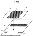
- FIG. 5 is a diagram illustrating a state before mounting the coil antenna on the mounting base, according to a method of manufacturing a coil antenna and a method of manufacturing a coil antenna package of a second embodiment.
- a method of manufacturing a coil antenna according to this embodiment includes a process of temporarily fixing the terminal ends 12a and 12b of the coil wire 12 to the coil antenna body 11 and a process of performing treatment on at least part of the coil wire 12 that comes into contact with connection parts (antenna connection patterns) 31 of a mounting base 30 on which the coil antenna 10 is to be mounted, so that the coil antenna 10 is electrically connectable to the mounting base 30, where the treatment forms pre-soldered parts 23.
- FIG. 3 illustrates an example of the coil antenna 10 that employs, as the coil antenna body 11, a magnetic material provided with SMT (surface mounting) lands 22 (antenna terminals) by printing a Ag thick film.
- the coil wire 12 is wound around the coil antenna body 11.
- the terminal ends 12a and 12b of the coil wire 12 are pre-soldered and are connected by high-temperature soldering or welded by spot welding to the SMT lands 22.
- the SMT lands 22 are not limited to particular dimensions.
- a dimension in the longitudinal direction of the coil antenna body 11, indicated by double-headed arrow e in FIG. 3 may be 1.0 mm and a dimension in a direction perpendicular to the transverse direction of the coil antenna body 11, indicated by double-headed arrow f in FIG. 3 , may be 1.0 mm.
- the coil antenna body 11 may employ sintered ferrite as a magnetic material.
- the coil antenna body 11 may be manufactured by performing half-cutting on the magnetic material, firing the magnetic material after printing SMT lands on half-cut sections, and applying PET resin having openings for the SMT lands onto the magnetic material.
- a coil antenna package is manufactured by joining the coil antenna 10 of FIG. 3 to the mounting base 30 as illustrated in FIG. 5 .
- the terminal ends 12a and 12b of the coil wire 12 are connected by high-temperature soldering or welded by spot welding to the SMT lands 22 formed on the coil antenna body 11, and the coil antenna 10 is thereafter disposed on the mounting base 30 so that the SMT lands 22 to which the coil wire 12 is connected come into contact with the antenna connection patterns 31, and is joined, together with other mounting parts, to the mounting base 30 with solder flow.
- FIG. 4 illustrates an example of the coil antenna 10 that employs, for example, a magnetic material of resin-coated ferrite as the coil antenna body 11.
- the coil wire 12 is wound around the coil antenna body 11, and the terminal ends 12a and 12b of the coil wire 12 are pre-soldered.
- the coil wire 12 is fixed to the coil antenna body 11 by thermocompression bonding to the resin coat.
- a coil antenna package is manufactured by joining the coil antenna 10 of FIG. 4 to the mounting base 30 as illustrated in FIG. 5 .
- the terminal ends 12a and 12b of the coil wire 12 are pre-soldered, and the coil antenna 10 is thereafter disposed on the mounting base 30 so that the pre-soldered parts 23 come into contact with the antenna connection patterns 31, and is joined, together with other mounting parts, to the mounting base 30 with solder flow.
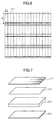
- FIG. 6 A description is given, with reference to FIG. 6, FIG. 7 , FIG. 8, FIG. 9 , FIG. 10 and FIG. 11 , of a third embodiment.
- the coil antenna 10 is manufactured where the coil antenna body 11 includes a plate-shaped magnetic material core 110 and a flexible printed circuit (FPC) board 111 including the SMT lands 22, and the terminal ends 12a and 12b of the coil wire 12 are temporarily fixed to the SMT lands 22.
- FPC flexible printed circuit
- the flexible printed circuit board 111 is an assembly board in which multiple elements are arranged. Each element is not limited to particular dimensions. For example, a dimension indicated by double-headed arrow a in FIG. 6 may be 6 mm, and a dimension indicated by double-headed arrow b in FIG. 6 may be 24 mm.
- the magnetic material core 110 is a ferrite core having a rectangular plate shape.
- a single-sided adhesive sheet 113 which is a polyimide with an adhesive material, is adhered to a first surface (a lower surface in the state of FIG. 7 ) of the magnetic material core 110.
- a heat-resistant double-sided adhesive sheet 112 is adhered to a second surface (an upper surface in the state of FIG. 7 ) of the magnetic material core 110.
- the flexible printed circuit board 111 is adhered to the magnetic material core 110 via the heat-resistant double-sided adhesive sheet 112, so that a laminate is obtained.
- the obtained laminate is divided along dividing lines indicated by dotted lines in FIG. 6 into individual pieces as illustrated in FIG. 8 .
- Each obtained individual piece is used for the manufacture of the coil antenna 10 as the coil antenna body 11.
- the coil wire 12 is wound around the coil antenna body 11, and the terminal ends 12a and 12b of the coil wire 12 are temporarily fixed to the SMT lands 22 by thermocompression bonding, so that the coil antenna 10 is formed.
- FIG. 9 and FIG. 10 illustrate examples of the coil antenna 10 according to this embodiment.
- the coil antenna 10 is not limited to particular dimensions.
- a dimension indicated by double-headed arrow c may be 2.0 mm
- a dimension indicated by double-headed arrow d may be 0.75 mm
- a dimension indicated by double-headed arrow e' may be 1.0 mm
- a dimension indicated by double-headed arrow f' may be 4.5 mm
- each of dimensions indicated by double-headed arrows f1 and f2 may be 2.0 mm.
- the dimension indicated by double-headed arrow c may be 2.0 mm
- the dimension indicated by double-headed arrow d may be 0.75 mm
- the dimension indicated by double-headed arrow e' may be 1.0 mm
- the dimension indicated by double-headed arrow f' may be 2.0 mm.
- the coil antenna 10 is disposed on the mounting base 30 so that the SMT lands 22 and the coil wire 12 come into contact with the antenna connection patterns 31 of the mounting base 30, and a solder flow process is performed to solder the coil antenna 10, together with other mounting parts such as chip resistor (CR)s 41 and a wafer-level chip size package (WLCSP) 42, to the mounting base 30.
- CR chip resistor
- WLCSP wafer-level chip size package
- solder flow process refers to causing an object to pass through a solder flow bath or a reflow apparatus.
- the coil antenna 10 manufactured according to any of the above-described manufacturing methods may be efficiently mounted while being kept thin. According to the coil antenna package manufactured according to any of the above-described manufacturing methods, an increase in thickness due to the joining of the coil antenna 10 and the mounting base 30 is suppressed. Accordingly, the manufactured coil antenna package is suitable as a component to be mounted on various types of portable terminals, such as radio communication devices including smartphones, that are desired to be reduced in size and thickness.
Landscapes
- Engineering & Computer Science (AREA)
- Manufacturing & Machinery (AREA)
- Microelectronics & Electronic Packaging (AREA)
- Computer Networks & Wireless Communication (AREA)
- Details Of Aerials (AREA)
- Coils Or Transformers For Communication (AREA)
Abstract
Description
- The present invention relates to methods of manufacturing a coil antenna and methods of manufacturing a coil antenna package.
- Recent years have seen a rapid diffusion of portable-terminal radio communications devices such as cellular phones, smartphones, and tablet personal computer (PC) terminals. Because these devices are both being reduced in size and becoming functionally more sophisticated at the same time, devices to be mounted on these devices also are required to be reduced in size and thickness. In particular, communication antennas to be mounted on these devices are required to be reduced in thickness.
- Antennas to be mounted on smartphones include loop antennas and spiral antennas. Of these, spiral antennas are believed to increase a communication distance.
- In the case of forming a low-profile antenna using a spiral antenna, it is necessary to reduce the thickness of a magnetic material that serves as a core around which a coil is wound. In the case of forming a core using a ferrite material having normal stiffness as a magnetic material, however, the core may be broken at the time of its manufacture or its incorporation into a product, thus being difficult to put to practical use.
- Therefore, techniques have been known that employ a bar-shaped or sheet-shaped magnetic material that holds small pieces of ferrite whose length of each side is a few millimeters in PET resin (for example, Patent Document 1 and Patent Document 2 listed below).
- Patent Document 1 discloses, in response to a demand for antenna flexibility, an antenna core that includes magnetic members each formed of a thin film magnetic material to which resin is applied, a flexible tube that hermetically seals a magnetic core part into which the magnetic members are stacked without being fixed to each other, and an oil solution interposed between the magnetic core part and the flexible tube. It is illustrated that according to this antenna core, it is possible to prevent generation of cracks and damage and to stabilize the shape, so that it is possible to obtain good antenna characteristics.
- Patent Document 2 discloses, in response to demands for shock resistance and a diversity of shapes, an antenna core formed of an insulating soft magnetic material that includes soft magnetic material powder and an organic binder. It is illustrated that as a result of using an insulating soft magnetic material having particular magnetic permeability frequency characteristics, a coil antenna including the antenna core obtains better characteristics than conventional coil antennas and has good shock resistance, processability, and mountability.
-
- [Patent Document 1]
Japanese Laid-Open Patent Application No. 2012-105092 - [Patent Document 2]
Japanese Laid-Open Patent Application No. 2005-317674 - While it is possible to reduce the thickness of a coil antenna (spiral antenna) that uses a flexible plate-shaped (sheet-shaped) magnetic material as a core, an antenna package formed by connecting the coil antenna to a board also is desired to be kept thin. Furthermore, it is also desired that the antenna package be manufactured at good efficiency.
- Patent Document 1 and Patent Document 2 are silent about a method of treating the terminal ends of a coil wire wound around an antenna core. The method of treating the terminal ends of a coil wire is believed to affect process efficiency and also the thickness of an antenna package.
- For example, soldering the terminal ends of a coil wire individually to an electronic board has the problem of making manufacture inefficient and making the reduction of thickness difficult.
- In view of the above-described problems, the present invention has an object of providing a method of manufacturing an efficiently mountable coil antenna using a flexible plate-shaped magnetic material as a core while keeping the coil antenna low-profile.
- According to an aspect of the present invention, a method of manufacturing a coil antenna that includes a flexible plate-shaped coil antenna body containing a magnetic material, and a coil wire wound around the coil antenna body in a direction perpendicular to a longitudinal direction of the coil antenna body so as to form a loop, includes the steps of temporarily fixing a terminal end of the coil wire to the coil antenna body and performing treatment on part of the coil wire that comes into contact with a connection part of a mounting base on which the coil antenna is to be mounted, so that the coil antenna is electrically connectable to the mounting base.
- According to an aspect of the present invention, a method of manufacturing a coil antenna package that includes a coil antenna including a flexible plate-shaped coil antenna body containing a magnetic material, and a coil wire wound around the coil antenna body in a direction perpendicular to a longitudinal direction of the coil antenna body so as to form a loop; and a mounting base on which the coil antenna is surface-mounted, the mounting base including a connection part at a position where the mounting base is connected to the coil antenna, includes the steps of temporarily fixing a terminal end of the coil wire to the coil antenna body, performing treatment on part of the coil wire that comes into contact with the connection part of the mounting base, so that the coil antenna is electrically connectable to the mounting base, and disposing the coil antenna on the mounting base so that the part of the coil wire comes into contact with the connection part, and joining the coil antenna to the mounting base with solder flow.
- According to an aspect of the present invention, a method of manufacturing an efficiently mountable coil antenna using a flexible plate-shaped magnetic material as a core while keeping the coil antenna low-profile is provided.
- According to an aspect of the present invention, a method of manufacturing a coil antenna package that suppresses an increase in thickness due to the joining of a coil antenna and a mounting base is provided.
-
-
FIG. 1 is an exterior perspective view of an example of a coil antenna before the coil antenna is mounted on a mounting base according to a method of manufacturing a coil antenna of a first embodiment. -
FIG. 2 is an exterior perspective view of another example of the coil antenna before the coil antenna is mounted on the mounting base according to the method of manufacturing a coil antenna of the first embodiment. -
FIG. 3 is a plan view of an example of the coil antenna before the coil antenna is mounted on the mounting base according to a second embodiment. -
FIG. 4 is a plan view of another example of the coil antenna before the coil antenna is mounted on the mounting base according to the second embodiment. -
FIG. 5 is a diagram illustrating a state before the coil antenna is mounted on the mounting base according to the second embodiment. -
FIG. 6 is a schematic plan view of an assembly board of a flexible printed circuit board according to a third embodiment. -
FIG. 7 is a diagram illustrating a configuration of a coil antenna body according to the third embodiment. -
FIG. 8 is a schematic diagram illustrating the coil antenna body in which the flexible printed circuit board is stacked on a magnetic material core according to the third embodiment. -
FIG. 9 is a schematic diagram illustrating an example of the coil antenna according to the third embodiment. -
FIG. 10 is a schematic diagram illustrating another example of the coil antenna according to the third embodiment. -
FIG. 11 is a diagram illustrating the coil antenna and other parts before being mounted on the mounting base according to the third embodiment. - A description is given below, with reference to the accompanying drawings, of embodiments of the present invention. In the following description, the same elements are referred to by the same reference numeral.
- According to an aspect of the present invention, a method of manufacturing a coil antenna that includes a flexible plate-shaped coil antenna body containing a magnetic material, and a coil wire wound around the coil antenna body in a direction perpendicular to a longitudinal direction of the coil antenna body so as to form a loop includes the steps of temporarily fixing a terminal end of the coil wire to the coil antenna body and performing treatment on part of the coil wire that comes into contact with a connection part of a mounting base on which the coil antenna is to be mounted, so that the coil antenna is electrically connectable to the mounting base.
- According to an aspect of the present invention, a method of manufacturing a coil antenna package that includes a coil antenna including a flexible plate-shaped coil antenna body containing a magnetic material, and a coil wire wound around the coil antenna body in a direction perpendicular to a longitudinal direction of the coil antenna body so as to form a loop; and a mounting base on which the coil antenna is surface-mounted, the mounting base including a connection part at a position where the mounting base is connected to the coil antenna, includes the steps of temporarily fixing a terminal end of the coil wire to the coil antenna body, performing treatment on part of the coil wire that comes into contact with the connection part of the mounting base, so that the coil antenna is electrically connectable to the mounting base, and disposing the coil antenna on the mounting base so that the part of the coil wire comes into contact with the connection part, and joining the coil antenna to the mounting base with solder flow.
-
FIG. 1 and FIG. 2 are perspective views each illustrating the exterior of a coil antenna before the coil antenna is mounted on a mounting base according to a method of manufacturing a coil antenna of a first embodiment. Referring toFIG. 1 and FIG. 2 , acoil antenna 10 includes a flexible plate-shapedcoil antenna body 11 containing a magnetic material, and acoil wire 12 wound around thecoil antenna body 11 in a transverse direction (a direction perpendicular to a longitudinal direction) of thecoil antenna body 11 so as to form a loop. - A method of manufacturing the
coil antenna 10 includes a process of temporarily fixingterminal ends coil wire 12 to thecoil antenna body 11 and a process of performing treatment on at least part of thecoil wire 12 that comes into contact with a connection part of a mounting base (not illustrated) on which thecoil antenna 10 is to be mounted, so that thecoil antenna 10 is electrically connectable to the mounting base. - Referring to
FIG. 1 and FIG. 2 , according to this embodiment, the terminal ends 12a and 12b of thecoil wire 12 of thecoil antenna 10 are temporarily fixed to a surface other than asurface 11a of thecoil antenna body 11 that faces (connects to) the mounting base when thecoil antenna 10 is disposed on the mounting base. - The
coil antenna body 11 includes asurface 11b that is opposite to thesurface 11a that faces the mounting base. Furthermore, thecoil antenna 10 includes antenna connectionpattern contact parts 20 at positions corresponding to connection parts (antenna connection patterns) formed on the mounting base. - The terminal ends 12a and 12b of the
coil wire 12 are temporarily fixed to a surface of thecoil antenna body 11 using an adhesive agent or the like. The surface to which the terminal ends 12a and 12b are temporarily fixed is preferably a surface of thecoil antenna body 11 adjoining thesurface 11a that faces (connects to) the mounting base as illustrated inFIG. 1 , in order to minimize an increase in the thickness of thecoil antenna 10 after its mounting on the mounting base. If such an arrangement is difficult for structural reasons, however, the surface to which the terminal ends 12a and 12b are temporarily fixed may be thesurface 11b opposite to thesurface 11a that connects to the mounting base as illustrated inFIG. 2 , on condition that the amount of application of an adhesive agent is minimized. - After temporary fixation of the
terminal ends coil wire 12, pre-treatment is performed on at least parts of thecoil wire 12, placed on thesurface 11a that connects to the mounting base, which parts are in the antenna connectionpattern contact parts 20 at positions corresponding to the antenna connection patterns formed on the mounting base. - The pre-treatment is performed so as to make the
coil antenna 10 and the mounting base easily connectable in a solder flow process, and includes, for example, formation of pre-soldered parts and removal of coats of coated copper wires. - According to this embodiment, the
coil antenna body 11 may be a flexible plate-shaped body containing a magnetic material. Examples of magnetic materials include ferrite, iron, nickel, cobalt, and their alloys, among which ferrite is preferable. - As the
coil wire 12, for example, a copper wire, preferably, a coated copper wire, may be used. -
FIG. 3 and FIG. 4 are plan views of a coil antenna before mounting the coil antenna on a mounting base andFIG. 5 is a diagram illustrating a state before mounting the coil antenna on the mounting base, according to a method of manufacturing a coil antenna and a method of manufacturing a coil antenna package of a second embodiment. - A method of manufacturing a coil antenna according to this embodiment includes a process of temporarily fixing the terminal ends 12a and 12b of the
coil wire 12 to thecoil antenna body 11 and a process of performing treatment on at least part of thecoil wire 12 that comes into contact with connection parts (antenna connection patterns) 31 of a mountingbase 30 on which thecoil antenna 10 is to be mounted, so that thecoil antenna 10 is electrically connectable to the mountingbase 30, where the treatment formspre-soldered parts 23. -
FIG. 3 illustrates an example of thecoil antenna 10 that employs, as thecoil antenna body 11, a magnetic material provided with SMT (surface mounting) lands 22 (antenna terminals) by printing a Ag thick film. Thecoil wire 12 is wound around thecoil antenna body 11. The terminal ends 12a and 12b of thecoil wire 12 are pre-soldered and are connected by high-temperature soldering or welded by spot welding to the SMT lands 22. - The SMT lands 22 are not limited to particular dimensions. For example, a dimension in the longitudinal direction of the
coil antenna body 11, indicated by double-headed arrow e inFIG. 3 , may be 1.0 mm and a dimension in a direction perpendicular to the transverse direction of thecoil antenna body 11, indicated by double-headed arrow f inFIG. 3 , may be 1.0 mm. - The
coil antenna body 11 may employ sintered ferrite as a magnetic material. In this case, thecoil antenna body 11 may be manufactured by performing half-cutting on the magnetic material, firing the magnetic material after printing SMT lands on half-cut sections, and applying PET resin having openings for the SMT lands onto the magnetic material. - A coil antenna package is manufactured by joining the
coil antenna 10 ofFIG. 3 to the mountingbase 30 as illustrated inFIG. 5 . - According to a method of manufacturing a coil antenna package of this embodiment, the terminal ends 12a and 12b of the
coil wire 12 are connected by high-temperature soldering or welded by spot welding to the SMT lands 22 formed on thecoil antenna body 11, and thecoil antenna 10 is thereafter disposed on the mountingbase 30 so that the SMT lands 22 to which thecoil wire 12 is connected come into contact with theantenna connection patterns 31, and is joined, together with other mounting parts, to the mountingbase 30 with solder flow. -
FIG. 4 illustrates an example of thecoil antenna 10 that employs, for example, a magnetic material of resin-coated ferrite as thecoil antenna body 11. Thecoil wire 12 is wound around thecoil antenna body 11, and the terminal ends 12a and 12b of thecoil wire 12 are pre-soldered. Thecoil wire 12 is fixed to thecoil antenna body 11 by thermocompression bonding to the resin coat. - A coil antenna package is manufactured by joining the
coil antenna 10 ofFIG. 4 to the mountingbase 30 as illustrated inFIG. 5 . - According to a method of manufacturing a coil antenna package of this embodiment, the terminal ends 12a and 12b of the
coil wire 12 are pre-soldered, and thecoil antenna 10 is thereafter disposed on the mountingbase 30 so that thepre-soldered parts 23 come into contact with theantenna connection patterns 31, and is joined, together with other mounting parts, to the mountingbase 30 with solder flow. - A description is given, with reference to
FIG. 6, FIG. 7 ,FIG. 8, FIG. 9 ,FIG. 10 andFIG. 11 , of a third embodiment. - According to a method of manufacturing a coil antenna of this embodiment, the
coil antenna 10 is manufactured where thecoil antenna body 11 includes a plate-shapedmagnetic material core 110 and a flexible printed circuit (FPC)board 111 including the SMT lands 22, and the terminal ends 12a and 12b of thecoil wire 12 are temporarily fixed to the SMT lands 22. - Referring to
FIG. 6 , the flexible printedcircuit board 111 is an assembly board in which multiple elements are arranged. Each element is not limited to particular dimensions. For example, a dimension indicated by double-headed arrow a inFIG. 6 may be 6 mm, and a dimension indicated by double-headed arrow b inFIG. 6 may be 24 mm. - Referring to
FIG. 7 , themagnetic material core 110 is a ferrite core having a rectangular plate shape. A single-sided adhesive sheet 113, which is a polyimide with an adhesive material, is adhered to a first surface (a lower surface in the state ofFIG. 7 ) of themagnetic material core 110. Meanwhile, a heat-resistant double-sided adhesive sheet 112 is adhered to a second surface (an upper surface in the state ofFIG. 7 ) of themagnetic material core 110. Then, the flexible printedcircuit board 111 is adhered to themagnetic material core 110 via the heat-resistant double-sided adhesive sheet 112, so that a laminate is obtained. - The obtained laminate is divided along dividing lines indicated by dotted lines in
FIG. 6 into individual pieces as illustrated inFIG. 8 . Each obtained individual piece is used for the manufacture of thecoil antenna 10 as thecoil antenna body 11. - The
coil wire 12 is wound around thecoil antenna body 11, and the terminal ends 12a and 12b of thecoil wire 12 are temporarily fixed to the SMT lands 22 by thermocompression bonding, so that thecoil antenna 10 is formed. -
FIG. 9 and FIG. 10 illustrate examples of thecoil antenna 10 according to this embodiment. - As illustrated in
FIG. 9 and FIG. 10 , by providing the two SMT lands 22 in total, one on each end side of thecoil antenna body 11, it becomes easy to maintain the horizontalness of thecoil antenna 10 relative to the mountingbase 30 when thesurface 11a of thecoil antenna body 11 on which the SMT lands 22 are provided and the mountingbase 30 are joined, so that it is possible to suppress variations in the antenna performance of thecoil antenna 10. By the arrangement illustrated inFIG. 10 , it is possible to stabilize the horizontalness of thecoil antenna 10 in its longitudinal direction. By the arrangement illustrated inFIG. 9 , it is possible to stabilize the horizontalness of thecoil antenna 10 in the transverse direction as well as the longitudinal direction of thecoil antenna 10, so that it is possible to attach thecoil antenna 10 to the mountingbase 30 while maintaining the horizontalness of thecoil antenna 10 with more reliability. - The
coil antenna 10 is not limited to particular dimensions. In the case ofFIG. 9 , when the external dimensions of thecoil antenna body 11 in its transverse direction and longitudinal direction indicated by double-headed arrows a and b are 6 mm and 24 mm, respectively, a dimension indicated by double-headed arrow c may be 2.0 mm, a dimension indicated by double-headed arrow d may be 0.75 mm, a dimension indicated by double-headed arrow e' may be 1.0 mm, a dimension indicated by double-headed arrow f' may be 4.5 mm, and each of dimensions indicated by double-headed arrows f1 and f2 may be 2.0 mm. - Furthermore, in the case of
FIG. 10 , likewise, when the external dimensions of thecoil antenna body 11 in its transverse direction and longitudinal direction indicated by double-headed arrows a and b are 6 mm and 24 mm, respectively, the dimension indicated by double-headed arrow c may be 2.0 mm, the dimension indicated by double-headed arrow d may be 0.75 mm, the dimension indicated by double-headed arrow e' may be 1.0 mm, and the dimension indicated by double-headed arrow f' may be 2.0 mm. - Then, as illustrated in
FIG. 11 , thecoil antenna 10 is disposed on the mountingbase 30 so that the SMT lands 22 and thecoil wire 12 come into contact with theantenna connection patterns 31 of the mountingbase 30, and a solder flow process is performed to solder thecoil antenna 10, together with other mounting parts such as chip resistor (CR)s 41 and a wafer-level chip size package (WLCSP) 42, to the mountingbase 30. - The "solder flow process" refers to causing an object to pass through a solder flow bath or a reflow apparatus.
- The
coil antenna 10 manufactured according to any of the above-described manufacturing methods may be efficiently mounted while being kept thin. According to the coil antenna package manufactured according to any of the above-described manufacturing methods, an increase in thickness due to the joining of thecoil antenna 10 and the mountingbase 30 is suppressed. Accordingly, the manufactured coil antenna package is suitable as a component to be mounted on various types of portable terminals, such as radio communication devices including smartphones, that are desired to be reduced in size and thickness. - All examples and conditional language provided herein are intended for pedagogical purposes of aiding the reader in understanding the invention and the concepts contributed by the inventors to further the art, and are not to be construed as limitations to such specifically recited examples and conditions, nor does the organization of such examples in the specification relate to a showing of the superiority or inferiority of the invention. Methods of manufacturing a coil antenna and methods of manufacturing a coil antenna package have been described in detail based on one or more embodiments of the present invention. It should be understood, however, that the various changes, substitutions, and alterations could be made hereto without departing from the spirit and scope of the present invention.
- The present application is based upon and claims the benefit of priority of
Japanese Patent Application No. 2013-237676, filed on November 18, 2013 -
- 10 coil antenna
- 11 coil antenna body
- 11a surface facing a mounting base
- 11b surface opposite to the surface facing a mounting base
- 110 magnetic material core
- 111 flexible printed circuit (FPC) board
- 112 heat-resistant double-sided adhesive sheet
- 113 single-sided adhesive sheet
- 12 coil wire
- 12a, 12b terminal end of the coil wire
- 20 antenna connection pattern contact part
- 22 SMT land
- 23 pre-soldered part
- 30 mounting base
- 31 antenna connection pattern
- 41 chip resistor (CR)
- 42 wafer-level chip size package (WLCSP)
Claims (7)
- A method of manufacturing a coil antenna, the coil antenna including a flexible plate-shaped coil antenna body containing a magnetic material, and a coil wire wound around the coil antenna body in a direction perpendicular to a longitudinal direction of the coil antenna body so as to form a loop, the method comprising the steps of:temporarily fixing a terminal end of the coil wire to the coil antenna body; andperforming treatment on a part of the coil wire that comes into contact with a connection part of a mounting base on which the coil antenna is to be mounted, so that the coil antenna is electrically connectable to the mounting base.
- The method of manufacturing a coil antenna as claimed in claim 1, wherein the terminal end of the coil wire is temporarily fixed to a surface of the coil antenna body other than a surface of the coil antenna body that faces the mounting base.
- The method of manufacturing a coil antenna as claimed in claim 1 or 2, wherein the terminal end of the coil wire is temporarily fixed to a surface of the coil antenna body adjoining a surface of the coil antenna body that faces the mounting base.
- The method of manufacturing a coil antenna as claimed in claim 1, wherein the terminal end of the coil wire is temporarily fixed to a surface of the coil antenna body that faces the mounting base.
- The method of manufacturing a coil antenna as claimed in claim 1, wherein the coil antenna body includes a plate-shaped magnetic material core and a flexible printed circuit board including an antenna terminal, and the terminal end of the coil wire is temporarily fixed to the antenna terminal.
- The method of manufacturing a coil antenna as claimed in any of claims 1 to 5, wherein the treatment pre-solders the part of the coil wire that comes into contact with the connection part of the mounting base.
- A method of manufacturing a coil antenna package, the coil antenna package including a coil antenna that includes a flexible plate-shaped coil antenna body containing a magnetic material, and a coil wire wound around the coil antenna body in a direction perpendicular to a longitudinal direction of the coil antenna body so as to form a loop; and a mounting base on which the coil antenna is surface-mounted, the mounting base including a connection part at a position where the mounting base is connected to the coil antenna, the method comprising the steps of:temporarily fixing a terminal end of the coil wire to the coil antenna body;performing treatment on a part of the coil wire that comes into contact with the connection part of the mounting base, so that the coil antenna is electrically connectable to the mounting base; anddisposing the coil antenna on the mounting base so that the part of the coil wire comes into contact with the connection part, and joining the coil antenna to the mounting base with solder flow.
Applications Claiming Priority (2)
| Application Number | Priority Date | Filing Date | Title |
|---|---|---|---|
| JP2013237676 | 2013-11-18 | ||
| PCT/JP2014/080371 WO2015072568A1 (en) | 2013-11-18 | 2014-11-17 | Method for manufacturing coil antenna and method for manufacturing coil antenna mounting body |
Publications (2)
| Publication Number | Publication Date |
|---|---|
| EP3073573A1 true EP3073573A1 (en) | 2016-09-28 |
| EP3073573A4 EP3073573A4 (en) | 2017-06-21 |
Family
ID=53057500
Family Applications (1)
| Application Number | Title | Priority Date | Filing Date |
|---|---|---|---|
| EP14861998.4A Withdrawn EP3073573A4 (en) | 2013-11-18 | 2014-11-17 | Method for manufacturing coil antenna and method for manufacturing coil antenna mounting body |
Country Status (6)
| Country | Link |
|---|---|
| US (1) | US20160261046A1 (en) |
| EP (1) | EP3073573A4 (en) |
| JP (1) | JP6197878B2 (en) |
| KR (1) | KR20160072198A (en) |
| CN (1) | CN105745789A (en) |
| WO (1) | WO2015072568A1 (en) |
Families Citing this family (6)
| Publication number | Priority date | Publication date | Assignee | Title |
|---|---|---|---|---|
| KR101658011B1 (en) * | 2016-01-08 | 2016-09-20 | 주식회사 아모텍 | Multi layer antenna module |
| US10886598B2 (en) * | 2016-11-16 | 2021-01-05 | Wits Co., Ltd. | Antenna module and electronic device having the same |
| KR102075779B1 (en) * | 2017-08-18 | 2020-02-11 | 주식회사 아모텍 | Ring type antenna and earphone having the same |
| EP3474378B1 (en) * | 2017-10-23 | 2021-03-17 | Premo, S.A. | Antenna for low frequency communication within a vehicle environment and low frequency communication system |
| MY206919A (en) * | 2019-07-01 | 2025-01-17 | Sumida Corp | Coil component, coil-component-equipped electric device, and coil component attaching method |
| CN115704873A (en) * | 2021-08-13 | 2023-02-17 | 上海联影医疗科技股份有限公司 | Radio frequency coil assembly |
Family Cites Families (20)
| Publication number | Priority date | Publication date | Assignee | Title |
|---|---|---|---|---|
| JPS6430305A (en) * | 1987-07-25 | 1989-02-01 | Fuji Electrochemical Co Ltd | Bar antenna |
| JPH10193849A (en) * | 1996-12-27 | 1998-07-28 | Rohm Co Ltd | Circuit chip mounted card and circuit chip module |
| JP2004032547A (en) * | 2002-06-27 | 2004-01-29 | Sony Corp | Antenna substrate and method of manufacturing the same |
| JP2004048136A (en) * | 2002-07-09 | 2004-02-12 | Mitsui Chemicals Inc | Thin antenna |
| RU2321926C2 (en) * | 2003-10-16 | 2008-04-10 | Сумида Корпорейшн | Antenna coil and antenna arrangement |
| KR100831804B1 (en) * | 2003-10-23 | 2008-05-28 | 가부시끼가이샤 도시바 | Inductive device and method for manufacturing same |
| US7307597B2 (en) * | 2004-03-17 | 2007-12-11 | Matsushita Electric Industrial Co., Ltd. | Antenna |
| JP3964401B2 (en) | 2004-04-27 | 2007-08-22 | Necトーキン株式会社 | Antenna core, coil antenna, watch, mobile phone, electronic device |
| FR2884681B1 (en) * | 2005-04-15 | 2007-06-22 | St Microelectronics Sa | ANTENNA FOR ELECTRONIC LABEL |
| JP3933191B1 (en) * | 2006-03-13 | 2007-06-20 | 株式会社村田製作所 | Portable electronic devices |
| JP3957000B1 (en) * | 2006-07-07 | 2007-08-08 | 株式会社村田製作所 | Antenna coil for board mounting and antenna device |
| JP4013987B1 (en) * | 2006-07-07 | 2007-11-28 | 株式会社村田製作所 | Antenna device |
| JP4940997B2 (en) * | 2007-02-27 | 2012-05-30 | カシオ計算機株式会社 | ANTENNA DEVICE, ANTENNA DEVICE MANUFACTURING METHOD, AND ELECTRONIC DEVICE |
| CN101657868B (en) * | 2007-04-13 | 2013-08-28 | 日立金属株式会社 | Magnetic core for antenna, method of manufacturing magnetic core for antenna, and antenna |
| KR101444785B1 (en) * | 2008-05-14 | 2014-09-26 | 엘지전자 주식회사 | Portable terminal |
| WO2010013992A1 (en) * | 2008-07-31 | 2010-02-04 | Eng Siang Koh | Flexible thin ribbon helical coil |
| EP2413424B1 (en) * | 2010-07-28 | 2016-05-04 | Panasonic Intellectual Property Management Co., Ltd. | Antenna device and communication apparatus including the same |
| JP2012105092A (en) * | 2010-11-10 | 2012-05-31 | Nakagawa Special Steel Co Inc | Antenna core, antenna using the antenna core, and manufacturing method of the antenna core |
| JP5885121B2 (en) * | 2011-10-06 | 2016-03-15 | 日立金属株式会社 | Antenna coil parts |
| JP5918609B2 (en) * | 2012-04-13 | 2016-05-18 | 株式会社吉川アールエフセミコン | Thin antenna coil |
-
2014
- 2014-11-17 EP EP14861998.4A patent/EP3073573A4/en not_active Withdrawn
- 2014-11-17 KR KR1020167012834A patent/KR20160072198A/en not_active Ceased
- 2014-11-17 WO PCT/JP2014/080371 patent/WO2015072568A1/en not_active Ceased
- 2014-11-17 JP JP2015547816A patent/JP6197878B2/en active Active
- 2014-11-17 CN CN201480062655.XA patent/CN105745789A/en active Pending
-
2016
- 2016-05-16 US US15/155,605 patent/US20160261046A1/en not_active Abandoned
Also Published As
| Publication number | Publication date |
|---|---|
| WO2015072568A1 (en) | 2015-05-21 |
| CN105745789A (en) | 2016-07-06 |
| KR20160072198A (en) | 2016-06-22 |
| US20160261046A1 (en) | 2016-09-08 |
| EP3073573A4 (en) | 2017-06-21 |
| JP6197878B2 (en) | 2017-09-20 |
| JPWO2015072568A1 (en) | 2017-03-16 |
Similar Documents
| Publication | Publication Date | Title |
|---|---|---|
| US20160261046A1 (en) | Method of manufacturing coil antenna and method of manufacturing coil antenna package | |
| US10998613B2 (en) | Chip antenna | |
| JP6256820B2 (en) | Flexible printed wiring board and method for manufacturing the flexible printed wiring board | |
| US10020582B2 (en) | Coil antenna and communication terminal device | |
| KR101719902B1 (en) | Antenna device and manufacturing method thereof | |
| US10373757B2 (en) | Printed circuit board, antenna, and wireless charging device | |
| CN206727226U (en) | Antenna device and electronic equipment | |
| EP2418729A2 (en) | Communication terminal | |
| KR102387826B1 (en) | Interposer and method thereof | |
| US20150222018A1 (en) | Antenna device and electronic apparatus | |
| CN104604026A (en) | Antenna device and communications device | |
| CN104025379A (en) | Antenna device, and communication terminal device | |
| JP2011029678A (en) | Antenna element and method for manufacturing the same | |
| KR102029491B1 (en) | Coil component and and board for mounting the same | |
| JP2017220850A (en) | ANTENNA DEVICE AND PORTABLE RADIO DEVICE EQUIPPED WITH THE SAME | |
| US10122065B2 (en) | Antenna device, card information medium, electronic apparatus, and method for manufacturing antenna device | |
| CN107453042B (en) | Chip type antenna | |
| JP2014027389A (en) | Antenna device | |
| JP2012039672A (en) | Antenna, antenna device and communication apparatus | |
| SK288795B6 (en) | Non-stationary magnetic field emitter | |
| JP2018160606A (en) | Transformer | |
| KR101647981B1 (en) | Winding type antenna using multi-layer wiring substrate | |
| JP2013115825A (en) | Antenna, antenna device and communication apparatus | |
| KR20170013570A (en) | Sheet having a function of electromagnetic shield and thermal emission | |
| KR20150024242A (en) | Solderable Intenna and Method for making the same |
Legal Events
| Date | Code | Title | Description |
|---|---|---|---|
| PUAI | Public reference made under article 153(3) epc to a published international application that has entered the european phase |
Free format text: ORIGINAL CODE: 0009012 |
|
| 17P | Request for examination filed |
Effective date: 20160513 |
|
| AK | Designated contracting states |
Kind code of ref document: A1 Designated state(s): AL AT BE BG CH CY CZ DE DK EE ES FI FR GB GR HR HU IE IS IT LI LT LU LV MC MK MT NL NO PL PT RO RS SE SI SK SM TR |
|
| AX | Request for extension of the european patent |
Extension state: BA ME |
|
| A4 | Supplementary search report drawn up and despatched |
Effective date: 20161108 |
|
| RIC1 | Information provided on ipc code assigned before grant |
Ipc: H01Q 7/06 20060101AFI20161102BHEP Ipc: H01Q 7/08 20060101ALI20161102BHEP |
|
| DAX | Request for extension of the european patent (deleted) | ||
| DA4 | Supplementary search report drawn up and despatched (deleted) | ||
| RA4 | Supplementary search report drawn up and despatched (corrected) |
Effective date: 20161108 |
|
| RIC1 | Information provided on ipc code assigned before grant |
Ipc: H01Q 1/24 20060101AFI20170522BHEP Ipc: H01Q 7/08 20060101ALI20170522BHEP Ipc: H01Q 7/06 20060101ALI20170522BHEP |
|
| 17Q | First examination report despatched |
Effective date: 20190820 |
|
| STAA | Information on the status of an ep patent application or granted ep patent |
Free format text: STATUS: THE APPLICATION IS DEEMED TO BE WITHDRAWN |
|
| 18D | Application deemed to be withdrawn |
Effective date: 20200103 |