EP3073566A1 - Mobile device and manufacturing method thereof - Google Patents
Mobile device and manufacturing method thereof Download PDFInfo
- Publication number
- EP3073566A1 EP3073566A1 EP16161113.2A EP16161113A EP3073566A1 EP 3073566 A1 EP3073566 A1 EP 3073566A1 EP 16161113 A EP16161113 A EP 16161113A EP 3073566 A1 EP3073566 A1 EP 3073566A1
- Authority
- EP
- European Patent Office
- Prior art keywords
- antenna structure
- ground
- mobile device
- ground branch
- branch
- Prior art date
- Legal status (The legal status is an assumption and is not a legal conclusion. Google has not performed a legal analysis and makes no representation as to the accuracy of the status listed.)
- Granted
Links
Images




Classifications
-
- H—ELECTRICITY
- H01—ELECTRIC ELEMENTS
- H01Q—ANTENNAS, i.e. RADIO AERIALS
- H01Q1/00—Details of, or arrangements associated with, antennas
- H01Q1/12—Supports; Mounting means
- H01Q1/22—Supports; Mounting means by structural association with other equipment or articles
- H01Q1/24—Supports; Mounting means by structural association with other equipment or articles with receiving set
- H01Q1/241—Supports; Mounting means by structural association with other equipment or articles with receiving set used in mobile communications, e.g. GSM
- H01Q1/242—Supports; Mounting means by structural association with other equipment or articles with receiving set used in mobile communications, e.g. GSM specially adapted for hand-held use
- H01Q1/243—Supports; Mounting means by structural association with other equipment or articles with receiving set used in mobile communications, e.g. GSM specially adapted for hand-held use with built-in antennas
-
- H—ELECTRICITY
- H01—ELECTRIC ELEMENTS
- H01Q—ANTENNAS, i.e. RADIO AERIALS
- H01Q1/00—Details of, or arrangements associated with, antennas
- H01Q1/36—Structural form of radiating elements, e.g. cone, spiral, umbrella; Particular materials used therewith
-
- H—ELECTRICITY
- H01—ELECTRIC ELEMENTS
- H01Q—ANTENNAS, i.e. RADIO AERIALS
- H01Q1/00—Details of, or arrangements associated with, antennas
- H01Q1/48—Earthing means; Earth screens; Counterpoises
-
- H—ELECTRICITY
- H01—ELECTRIC ELEMENTS
- H01Q—ANTENNAS, i.e. RADIO AERIALS
- H01Q13/00—Waveguide horns or mouths; Slot antennas; Leaky-waveguide antennas; Equivalent structures causing radiation along the transmission path of a guided wave
- H01Q13/10—Resonant slot antennas
-
- H—ELECTRICITY
- H01—ELECTRIC ELEMENTS
- H01Q—ANTENNAS, i.e. RADIO AERIALS
- H01Q13/00—Waveguide horns or mouths; Slot antennas; Leaky-waveguide antennas; Equivalent structures causing radiation along the transmission path of a guided wave
- H01Q13/10—Resonant slot antennas
- H01Q13/106—Microstrip slot antennas
-
- H—ELECTRICITY
- H01—ELECTRIC ELEMENTS
- H01Q—ANTENNAS, i.e. RADIO AERIALS
- H01Q21/00—Antenna arrays or systems
- H01Q21/28—Combinations of substantially independent non-interacting antenna units or systems
-
- H—ELECTRICITY
- H01—ELECTRIC ELEMENTS
- H01Q—ANTENNAS, i.e. RADIO AERIALS
- H01Q5/00—Arrangements for simultaneous operation of antennas on two or more different wavebands, e.g. dual-band or multi-band arrangements
- H01Q5/20—Arrangements for simultaneous operation of antennas on two or more different wavebands, e.g. dual-band or multi-band arrangements characterised by the operating wavebands
-
- H—ELECTRICITY
- H01—ELECTRIC ELEMENTS
- H01Q—ANTENNAS, i.e. RADIO AERIALS
- H01Q5/00—Arrangements for simultaneous operation of antennas on two or more different wavebands, e.g. dual-band or multi-band arrangements
- H01Q5/30—Arrangements for providing operation on different wavebands
-
- H—ELECTRICITY
- H01—ELECTRIC ELEMENTS
- H01Q—ANTENNAS, i.e. RADIO AERIALS
- H01Q5/00—Arrangements for simultaneous operation of antennas on two or more different wavebands, e.g. dual-band or multi-band arrangements
- H01Q5/30—Arrangements for providing operation on different wavebands
- H01Q5/307—Individual or coupled radiating elements, each element being fed in an unspecified way
- H01Q5/342—Individual or coupled radiating elements, each element being fed in an unspecified way for different propagation modes
- H01Q5/35—Individual or coupled radiating elements, each element being fed in an unspecified way for different propagation modes using two or more simultaneously fed points
-
- H—ELECTRICITY
- H01—ELECTRIC ELEMENTS
- H01Q—ANTENNAS, i.e. RADIO AERIALS
- H01Q5/00—Arrangements for simultaneous operation of antennas on two or more different wavebands, e.g. dual-band or multi-band arrangements
- H01Q5/40—Imbricated or interleaved structures; Combined or electromagnetically coupled arrangements, e.g. comprising two or more non-connected fed radiating elements
-
- H—ELECTRICITY
- H01—ELECTRIC ELEMENTS
- H01Q—ANTENNAS, i.e. RADIO AERIALS
- H01Q5/00—Arrangements for simultaneous operation of antennas on two or more different wavebands, e.g. dual-band or multi-band arrangements
- H01Q5/50—Feeding or matching arrangements for broad-band or multi-band operation
-
- H—ELECTRICITY
- H01—ELECTRIC ELEMENTS
- H01Q—ANTENNAS, i.e. RADIO AERIALS
- H01Q9/00—Electrically-short antennas having dimensions not more than twice the operating wavelength and consisting of conductive active radiating elements
- H01Q9/04—Resonant antennas
- H01Q9/0407—Substantially flat resonant element parallel to ground plane, e.g. patch antenna
- H01Q9/0442—Substantially flat resonant element parallel to ground plane, e.g. patch antenna with particular tuning means
-
- H—ELECTRICITY
- H01—ELECTRIC ELEMENTS
- H01Q—ANTENNAS, i.e. RADIO AERIALS
- H01Q9/00—Electrically-short antennas having dimensions not more than twice the operating wavelength and consisting of conductive active radiating elements
- H01Q9/04—Resonant antennas
- H01Q9/30—Resonant antennas with feed to end of elongated active element, e.g. unipole
- H01Q9/42—Resonant antennas with feed to end of elongated active element, e.g. unipole with folded element, the folded parts being spaced apart a small fraction of the operating wavelength
Definitions
- the subject application generally relates to a mobile device, and more specifically, to a mobile device and an antenna structure therein.
- mobile devices such as portable computers, mobile phones, multimedia players, and other hybrid functional portable electronic devices have become more common.
- mobile devices usually can perform wireless communication functions.
- Some devices cover a large wireless communication area; these include mobile phones using 2G, 3G, and LTE (Long Term Evolution) systems and using frequency bands of 700MHz, 850MHz, 900MHz, 1800MHz, 1900MHz, 2100MHz, 2300MHz, and 2600MHz.
- Some devices cover a small wireless communication area; these include mobile phones using Wi-Fi and Bluetooth systems and using frequency bands of 2.4GHz, 5.2GHz, and 5.8GHz.
- a mobile phone usually has a limited amount of inner space. However, more and more antennas should be arranged in the mobile phone to operate in different bands. The number of electronic components other than the antennas, in the mobile phone, has not been reduced. Accordingly, each antenna is close to the electronic components, negatively affecting the antenna efficiency and bandwidths thereof.
- the subject application is directed to a mobile device including a ground plane, a ground branch, a supporting element, and a circuit element.
- the ground branch is coupled to the ground plane.
- a slot is formed between the ground branch and the ground plane.
- the supporting element is disposed above the ground branch, and a vertical projection of the supporting element at least partially overlaps the ground branch.
- the circuit element is coupled between the ground branch and the ground plane.
- a first antenna structure is formed by the ground branch and excited by a first signal source.
- a second antenna structure is disposed on the supporting element and is excited by a second signal source.
- the ground branch substantially has an L-shape.
- the slot substantially has a straight-line shape.
- the slot has an open end and a closed end.
- the supporting element is made of a nonconductive material.
- the whole vertical projection of the supporting element is inside the ground branch.
- the mobile device further includes a first matching circuit and a second matching circuit.
- the first signal source is coupled through the first matching circuit to the first antenna structure.
- the second signal source is coupled through the second matching circuit to the second antenna structure.
- the circuit element is disposed inside the slot.
- the circuit element is a variable capacitor.
- a capacitance of the variable capacitor is from about 0.5pF to about 3.3pF.
- the first antenna structure is used as a reference ground plane of the second antenna structure.
- the second antenna structure includes a first radiation element and a second radiation element.
- the first radiation element is coupled to the second signal source.
- the second radiation element is coupled to the ground branch.
- the second antenna structure further includes a first connection element and a second connection element.
- the first radiation element is coupled through the first connection element to the second signal source.
- the second radiation element is coupled through the second connection element to the ground branch.
- first connection element and the second connection element are both substantially perpendicular to the ground branch and the supporting element.
- the first antenna structure operates in a low-frequency band
- the second antenna structure operates in a medium-frequency band and a high-frequency band.
- the low-frequency band is from about 698MHz to about 960MHz.
- the medium-frequency band is from about 1710MHz to about 2170MHz, and the high-frequency band is from 2300MHz to 2700MHz.
- the mobile device further includes one or more electronic components, disposed on the ground branch.
- the electronic components include a speaker, a camera, and/or a headphone jack.
- the subject application is directed to a method for manufacturing a mobile device, including the steps of: providing a ground plane and a ground branch, wherein the ground branch is coupled to the ground plane, and a slot is formed between the ground branch and the ground plane; disposing a supporting element above the ground branch, wherein the vertical projection of the supporting element at least partially overlaps the ground branch; coupling a circuit element between the ground branch and the ground plane; using the ground branch to form a first antenna structure, wherein the first antenna structure is excited by a first signal source; and disposing a second antenna structure on the supporting element, wherein the second antenna structure is excited by a second signal source.
- the subject application is directed to a mobile device including a ground plane, a ground branch, a circuit element, and a switch element.
- the ground branch is coupled to the ground plane.
- a slot is formed between the ground branch and the ground plane.
- the circuit element is coupled between the ground branch and the ground plane.
- the switch element is coupled between the ground branch and the ground plane.
- a first antenna structure is formed by the ground branch and excited by a first signal source.
- a second antenna structure is coupled to the ground branch and excited by a second signal source.
- the second antenna structure is adjacent to an open end of the ground branch.
- the first antenna structure and the second antenna structure are disposed on a same plane.
- the first antenna structure and the second antenna structure are disposed on two respective perpendicular planes.
- the circuit element is disposed at a central portion of the slot.
- the switch element is adjacent to a closed end of the slot.
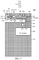
- FIG. 1 is a top view of a mobile device 100 according to an embodiment of the subject application.
- the mobile device 100 may be a smartphone, a tablet computer, or a notebook computer.
- the mobile device 100 includes a ground plane 110, a ground branch 120, a supporting element 140, a circuit element 150, a first signal source 191, and a second signal source 192.
- the ground plane 110 and the ground branch 120 may be made of metal materials, such as copper, silver, aluminum, iron, or their alloys. In some embodiments, the ground plane 110 and the ground branch 120 are integrated with a portion of a metal housing of the mobile device 100.
- the supporting element 140 may be made of a nonconductive material, such as a plastic material or other dielectric materials.
- the circuit element 150 may be an active element. It should be understood that the mobile device 100 may further include other components, such as a housing, a touch input control module, a display module, an RF (Radio Frequency) module, a processor module, a control module, and a power supply module, etc. (not shown).
- a housing such as a touch input control module, a display module, an RF (Radio Frequency) module, a processor module, a control module, and a power supply module, etc. (not shown).
- the ground branch 120 has a first end 121 and a second end 122.
- the first end 121 of the ground branch 120 is coupled to a ground plane 110, and the second end 122 of the ground branch 120 is open.
- a slot 130 is formed between the ground branch 120 and the ground plane 110.
- the slot 130 has an open end and a closed end.
- the ground branch 120 may substantially have an L-shape.
- the slot 130 may substantially have a straight-line shape.
- the supporting element 140 is disposed above the ground branch 120.
- a vertical projection of the supporting element 140 at least partially overlaps the ground branch 120. In the embodiment of FIG. 1 , the whole vertical projection of the supporting element 140 is inside the ground branch 120.
- the supporting element 140 may be directly affixed to a surface of the ground branch 120, or the supporting element 140 may be separate from the ground branch 120 and substantially parallel to the ground branch 120. If the supporting element 140 is separate from the ground branch 120, the ground plane 110 and the ground branch 120 may be integrated with a portion (e.g., a back cover) of a metal housing of the mobile device 100, and the supporting element 140 may be integrated with a front sound output element (not shown) (e.g., a sound hole of a speaker, or an earphone) of the mobile device 100, as a portion of a housing.
- a front sound output element not shown
- a first antenna structure 160 is formed by the ground branch 120.
- a first signal source 191 is coupled to a first feeding point FP1 on the first antenna structure 160, such that the first antenna structure 160 is excited by the first signal source 191.
- a second antenna structure 170 is disposed on the supporting element 140.
- a second signal source 192 is coupled to a second feeding point FP2 on the second antenna structure 170, such that the second antenna structure 170 is excited by the second signal source 192.
- the first signal source 191 and the second signal source 192 may be two RF (Radio Frequency) modules of the mobile device 100.
- the first antenna structure 160 is a PIFA (Planar Inverted F Antenna), but the second antenna structure 170 may be any type.
- the second antenna structure 170 may be a monopole antenna, a dipole antenna, a loop antenna, a coupling-feed antenna, or a patch antenna, and it may be directly printed on the supporting element 140.
- the circuit element 150 is coupled between the ground branch 120 and the ground plane 110, and is configured to adjust the impedance matching of the first antenna structure 160 and the second antenna structure 170.
- the circuit element 150 may be disposed inside the slot 130.
- the circuit element 150 is a variable capacitor, such as a varactor diode.
- a capacitance of the variable capacitor is from about 0.5pF to about 3.3pF.
- the capacitance of the variable capacitor may be adjusted according a control signal.
- the control signal may be generated by a processor, or by a detector according to the frequency of electromagnetic waves (not shown) detected nearby.
- the first antenna structure 160 operates in a low-frequency band
- the second antenna structure 170 operates in a medium-frequency band and a high-frequency band.
- the low-frequency band may be from about 698MHz to about 960MHz
- the medium-frequency band may be from about 1710MHz to about 2170MHz
- the high-frequency band may be from 2300MHz to 2700MHz.
- the mobile device 100 of the subject application may cover at least the wide frequency bands of LTE B12/B17/B13/B20/GSM850/900/DCS1800/PCS1900/UMTS and LTE B38/40/41/7.
- the first antenna structure 160 and the second antenna structure 170 may have antenna efficiency which is greater than 50% in the above low-frequency, medium-frequency, and high-frequency bands, and such antenna efficiency can meet the requirements of general mobile communication.
- the first antenna structure 160 and the second antenna structure 170 can further support CA (Carrier Aggregation) technology.
- the first antenna structure 160 (i.e. the ground branch 120) is used as a reference ground plane of the second antenna structure 170.
- the reference ground plane of the first antenna structure 160 is the ground plane 110.
- the second antenna structure 170 is positioned at a resonator of the first antenna structure 160 and well integrated therewith, the two antenna structures can share the antenna clearance region of the mobile device 100, thereby effectively reducing the total antenna size of the proposed mobile device 100.
- the first antenna structure 160 and the second antenna structure 170 can have different effective ground point and different operation frequency, so as to significantly enhance the isolation between the first antenna structure 160 and the second antenna structure 170. Therefore, the mobile device and the antenna structure of the subject application have at least the advantages of having a small size, wideband operation, and high isolation, and they are suitable for application in a variety of small-sized mobile communication devices.
- FIG. 2A is a top view of a mobile device 200 according to an embodiment of the subject application.
- FIG. 2B is a sectional view of the mobile device 200 according to an embodiment of the subject application. Please refer to FIG. 2A and FIG. 2B together.
- FIG. 2A and FIG. 2B are similar to FIG. 1 .
- the mobile device 200 includes a ground plane 110, a ground branch 120, a supporting element 240, a circuit element 150, a first matching circuit 281, a second matching circuit 282, and an RF (Radio Frequency) module 290.
- the structures and functions of the ground plane 110, the ground branch 120, the supporting element 240, and the circuit element 150 have been discussed in the embodiments of FIG. 1 .
- the mobile device 200 also includes a first antenna structure 260 and a second antenna structure 270.
- the RF module 290 has a first port PR1 and a second port PR2.
- the first port PR1 of the RF module 290 is coupled through the first matching circuit 281 to a first feeding point FP1 on the first antenna structure 260.
- the second port PR2 of the RF module 290 is coupled through the second matching circuit 282 to a second feeding point FP2 on the second antenna structure 270.
- the first port PR1 and the second port PR2 of the RF module 290 are used as the aforementioned first signal source 191 and the second signal source 192, and they are configured to excite the first antenna structure 260 and the second antenna structure 270, respectively, such that the first antenna structure 260 and the second antenna structure 270 can operate in a low-frequency band, a medium-frequency band, and a high-frequency band.
- the first matching circuit 281 and the second matching circuit 282 may each include one or more capacitors and/or one or more inductors (e.g., chip capacitors and chip inductors), so as to adjust the impedance matching and operation frequency of the first antenna structure 260 and the second antenna structure 270.
- the first matching circuit 281 and the second matching circuit 282 may each be formed by a capacitor and an inductor coupled in series, or by a capacitor and an inductor coupled in parallel. It should be understood that the subject application is not limited to the above examples.
- the first antenna structure 260 is a PIFA
- the second antenna structure 270 is a coupling-feed antenna.
- the second antenna structure 270 includes a first radiation element 271, a second radiation element 272, a first connection element 273, and a second connection element 274.
- the first radiation element 271 is separate from the second radiation element 272.
- the first radiation element 271 is coupled through the first connection element 273 to the second port PR2 of the RF module 290.
- the second radiation element 272 is coupled through the second connection element 274 to the ground branch 120.
- the first connection element 273 and the second connection element 274 are both substantially perpendicular to the ground branch 120 and the supporting element 240.
- Each of the first connection element 273 and the second connection element 274 may be a pogo pin or a metal spring.
- the second radiation element 272 is disposed adjacent to the first radiation element 271, and is excited by the first radiation element 271 through a mutual coupling mechanism.
- the first radiation element 271 may substantially be shaped like a question mark.
- the second radiation element 272 may substantially have a J-shape.
- the first radiation element 271 and the second radiation element 272 are completely separate from each other.
- any one of the first radiation element 271 and the second radiation element 272 has a different shape, such as a straight-line shape, an L-shape, an F-shape, or an S-shape, and the first radiation element 271 and the second radiation element 272 may be coupled to each other.
- Other features of the mobile device 200 of FIG. 2A and FIG. 2B are similar to those of the mobile device 100 of FIG. 1 . Accordingly, the two embodiments can achieve similar levels of performance.
- FIG. 3 is a top view of a mobile device 300 according to an embodiment of the subject application.
- FIG. 3 is similar to FIG. 2 .
- the mobile device 300 further includes one or more electronic components, such as a speaker 310, a camera 320, and/or a headphone jack 330.
- the electronic components are disposed on a first antenna structure 260 (i.e., the ground branch 120) of the mobile device 300, and may be used as a portion of the first antenna structure 260. Accordingly, the electronic components do not influence the radiation performance of the first antenna structure 260 very much.
- the first antenna structure 260 may load the electronic components and may be appropriately integrated with them, thereby reducing the use of the inner design space of the mobile device 300.
- the electronic components may be coupled through a wiring region 344 to a processor module and a control module (not shown) of the mobile device 300.
- Other features of the mobile device 300 of FIG. 3 are similar to those of the mobile device 200 of FIG. 2 . Accordingly, the two embodiments can achieve similar levels of performance.
- FIG. 4A is a diagram of a VSWR (Voltage Standing Wave Ratio) of the first antenna structure 260 of the mobile device 200 according to an embodiment of the subject application.
- FIG. 4B is a diagram of a VSWR of the second antenna structure 270 of the mobile device 200 according to an embodiment of the subject application. Please refer to FIG. 4A and FIG. 4B together.
- the horizontal axis represents the operation frequency (MHz), and the vertical axis represents the VSWR.
- a first curve CC1 represents the characteristic of the above antenna structures when the circuit element 150 has a capacitance of 0.75pF.
- a second curve CC2 represents the characteristic of the above antenna structures when the circuit element 150 has a capacitance of 1 pF.
- a third curve CC3 represents the characteristic of the above antenna structures when the circuit element 150 has a capacitance of 1.5pF.
- a fourth curve CC4 represents the characteristic of the above antenna structures when the circuit element 150 has a capacitance of 2.2pF.
- a fifth curve CC5 represents the characteristic of the above antenna structures when the circuit element 150 has a capacitance of 3.3pF.
- the change of the capacitance of the circuit element 150 has little impact on the second antenna structure 270. Therefore, by appropriately controlling the impedance value of the circuit element 150, the mobile device 200 of the subject application can achieve multi-band operations and wideband operations, without changing the total size of the antenna structures.
- FIG. 5 is a diagram of isolation between the first antenna structure 260 and the second antenna structure 270 of the mobile device 200 according to an embodiment of the subject application.
- the horizontal axis represents the operation frequency (MHz), and the vertical axis represents the isolation (S21) (dB).
- a sixth curve CC6 represents the characteristic of the above isolation when the circuit element 150 has a capacitance of 0.75pF.
- a seventh curve CC7 represents the characteristic of the above isolation when the circuit element 150 has a capacitance of 1 pF.
- An eighth curve CC8 represents the characteristic of above isolation when the circuit element 150 has a capacitance of 1.5pF.
- a ninth curve CC9 represents the characteristic of the above isolation when the circuit element 150 has a capacitance of 2.2pF.
- a tenth curve CC10 represents the characteristic of the above isolation when the circuit element 150 has a capacitance of 3.3pF. According to the measurement of FIG. 5 , when the capacitance of the circuit element 150 is increased, the isolation between the first antenna structure 260 and the second antenna structure 270 is improved; and when the capacitance of the circuit element 150 is decreased, the isolation between the first antenna structure 260 and the second antenna structure 270 is reduced. Accordingly, by appropriately controlling the impedance value of the circuit element 150, the mobile device 200 of the subject application can enhance the isolation between the first antenna structure 260 and the second antenna structure 270, thereby eliminating signal transmission interference. In alternative embodiments, when the circuit element 150 is moved toward the left open end of the slot 130, the isolation between the first antenna structure 260 and the second antenna structure 270 may be enhanced further, in particular to the medium-frequency band and the high-frequency band.
- FIG. 6 is a flowchart of a method for manufacturing a mobile device according to an embodiment of the subject application.
- the manufacturing method may include the following steps.
- step S610 a ground plane and a ground branch are provided.
- the ground branch is coupled to the ground plane.
- a slot is formed between the ground branch and the ground plane.
- step S620 a supporting element is disposed above the ground branch.
- a vertical projection of the supporting element at least partially overlaps the ground branch.
- a circuit element is coupled between the ground branch and the ground plane.
- the ground branch is used to form a first antenna structure.
- the first antenna structure is excited by a first signal source.
- step S650 a second antenna structure is disposed on the supporting element.
- the second antenna structure is excited by a second signal source.
- FIG. 7 is a top view of a mobile device 700 according to an embodiment of the subject application.
- FIG. 7 is similar to FIG. 2A and FIG. 2B .
- the mobile device 700 includes a ground plane 110, a ground branch 720, a circuit element 750, a switch element 780, and an RF module 290.
- the ground branch 720 has a first end 721 and a second end 722.
- the first end 721 of the ground branch 720 is coupled to the ground plane 110, and the second end 722 of the ground branch 720 is open.
- a slot 730 is formed between the ground branch 720 and the ground plane 110.
- the slot 730 has an open end and a closed end.
- the circuit element 750 is coupled between the ground branch 720 and the ground plane 110.
- the circuit element 750 may be a variable capacitor.
- the circuit element 750 may be disposed at a central portion of the slot 730.
- the switch element 780 is coupled between the ground branch 720 and the ground plane 110.
- the switch element 780 may be adjacent to a closed end of the slot 730.
- a first antenna structure 760 is formed by the ground branch 720.
- the first antenna structure 760 is excited by a first port PR1 of the RF module 290 through the circuit element 750.
- a second antenna structure 770 is coupled to the ground branch 720.
- the second antenna structure 770 is excited by a second port PR2 of the RF module 290.
- the second antenna structure 770 is disposed adjacent to the second end 722 of the ground branch 720.
- the second end 722 of the ground branch 720 may have a corner notch
- the second antenna structure 770 may include a T-shaped or straight-line-shaped radiator disposed in the corner notch.
- the first antenna structure 760 is used as a reference ground plane of the second antenna structure 770.
- the first antenna structure 760 operates in a low-frequency band and a medium-frequency band
- the second antenna structure 770 operates in a high-frequency band.
- the low-frequency band may be from about 698MHz to about 960MHz
- the medium-frequency band may be from about 1710MHz to about 2170MHz
- the high-frequency band may be from 2300MHz to 2700MHz.
- the switch element 780 By operating the switch element 780 in a closed state or an open state, and changing the variable capacitance of the circuit element 750, the first antenna structure 760 and the second antenna structure 770 can generate three different resonant paths LL1, LL2, and LL3, so as to respectively cover the low-frequency band, medium-frequency band, and high-frequency band above.
- the first antenna structure 760 and the second antenna structure 770 are disposed on the same plane, but the subject application is not limited thereto.
- the first antenna structure 760 and the second antenna structure 770 may be disposed at two respective perpendicular planes.
- the first antenna structure 760 may be formed on a back cover of a mobile device
- the second antenna structure 770 may be formed on a top cover of the mobile device (not shown).
- the back cover and the top cover may be perpendicular to each other.
- Other features of the mobile device 700 of FIG. 7 are similar to those of the mobile device 200 of FIG. 2A and FIG. 2B . Accordingly, the two embodiments can achieve similar levels of performance.
- the mobile device and antenna structure of the subject application are not limited to the configurations of FIGS. 1-7 .
- the subject application may merely include any one or more features of any one or more embodiments of FIGS. 1-7 . In other words, not all of the features displayed in the figures should be implemented in the mobile device and antenna structure of the subject application.
Landscapes
- Physics & Mathematics (AREA)
- Electromagnetism (AREA)
- Engineering & Computer Science (AREA)
- Computer Networks & Wireless Communication (AREA)
- Support Of Aerials (AREA)
- Waveguide Aerials (AREA)
- Telephone Set Structure (AREA)
Abstract
Description
- The subject application generally relates to a mobile device, and more specifically, to a mobile device and an antenna structure therein.
- With the advancement of mobile communication technology, mobile devices such as portable computers, mobile phones, multimedia players, and other hybrid functional portable electronic devices have become more common. To satisfy the demand of users, mobile devices usually can perform wireless communication functions. Some devices cover a large wireless communication area; these include mobile phones using 2G, 3G, and LTE (Long Term Evolution) systems and using frequency bands of 700MHz, 850MHz, 900MHz, 1800MHz, 1900MHz, 2100MHz, 2300MHz, and 2600MHz. Some devices cover a small wireless communication area; these include mobile phones using Wi-Fi and Bluetooth systems and using frequency bands of 2.4GHz, 5.2GHz, and 5.8GHz.
- A mobile phone usually has a limited amount of inner space. However, more and more antennas should be arranged in the mobile phone to operate in different bands. The number of electronic components other than the antennas, in the mobile phone, has not been reduced. Accordingly, each antenna is close to the electronic components, negatively affecting the antenna efficiency and bandwidths thereof.
- In a preferred embodiment, the subject application is directed to a mobile device including a ground plane, a ground branch, a supporting element, and a circuit element. The ground branch is coupled to the ground plane. A slot is formed between the ground branch and the ground plane. The supporting element is disposed above the ground branch, and a vertical projection of the supporting element at least partially overlaps the ground branch. The circuit element is coupled between the ground branch and the ground plane. A first antenna structure is formed by the ground branch and excited by a first signal source. A second antenna structure is disposed on the supporting element and is excited by a second signal source.
- In some embodiments, the ground branch substantially has an L-shape.
- In some embodiments, the slot substantially has a straight-line shape.
- In some embodiments, the slot has an open end and a closed end.
- In some embodiments, the supporting element is made of a nonconductive material.
- In some embodiments, the whole vertical projection of the supporting element is inside the ground branch.
- In some embodiments, the mobile device further includes a first matching circuit and a second matching circuit. The first signal source is coupled through the first matching circuit to the first antenna structure. The second signal source is coupled through the second matching circuit to the second antenna structure.
- In some embodiments, the circuit element is disposed inside the slot.
- In some embodiments, the circuit element is a variable capacitor.
- In some embodiments, a capacitance of the variable capacitor is from about 0.5pF to about 3.3pF.
- In some embodiments, the first antenna structure is used as a reference ground plane of the second antenna structure.
- In some embodiments, the second antenna structure includes a first radiation element and a second radiation element. The first radiation element is coupled to the second signal source. The second radiation element is coupled to the ground branch.
- In some embodiments, the second antenna structure further includes a first connection element and a second connection element. The first radiation element is coupled through the first connection element to the second signal source. The second radiation element is coupled through the second connection element to the ground branch.
- In some embodiments, the first connection element and the second connection element are both substantially perpendicular to the ground branch and the supporting element.
- In some embodiments, the first antenna structure operates in a low-frequency band, and the second antenna structure operates in a medium-frequency band and a high-frequency band.
- In some embodiments, the low-frequency band is from about 698MHz to about 960MHz.
- In some embodiments, the medium-frequency band is from about 1710MHz to about 2170MHz, and the high-frequency band is from 2300MHz to 2700MHz.
- In some embodiments, the mobile device further includes one or more electronic components, disposed on the ground branch.
- In some embodiments, the electronic components include a speaker, a camera, and/or a headphone jack.
- In a preferred embodiment, the subject application is directed to a method for manufacturing a mobile device, including the steps of: providing a ground plane and a ground branch, wherein the ground branch is coupled to the ground plane, and a slot is formed between the ground branch and the ground plane; disposing a supporting element above the ground branch, wherein the vertical projection of the supporting element at least partially overlaps the ground branch; coupling a circuit element between the ground branch and the ground plane; using the ground branch to form a first antenna structure, wherein the first antenna structure is excited by a first signal source; and disposing a second antenna structure on the supporting element, wherein the second antenna structure is excited by a second signal source.
- In a preferred embodiment, the subject application is directed to a mobile device including a ground plane, a ground branch, a circuit element, and a switch element. The ground branch is coupled to the ground plane. A slot is formed between the ground branch and the ground plane. The circuit element is coupled between the ground branch and the ground plane. The switch element is coupled between the ground branch and the ground plane. A first antenna structure is formed by the ground branch and excited by a first signal source. A second antenna structure is coupled to the ground branch and excited by a second signal source.
- In some embodiments, the second antenna structure is adjacent to an open end of the ground branch.
- In some embodiments, the first antenna structure and the second antenna structure are disposed on a same plane.
- In some embodiments, the first antenna structure and the second antenna structure are disposed on two respective perpendicular planes.
- In some embodiments, the circuit element is disposed at a central portion of the slot.
- In some embodiments, the switch element is adjacent to a closed end of the slot.
- The subject application can be more fully understood by reading the subsequent detailed description and examples with references made to the accompanying drawings, wherein:
-
FIG. 1 is a top view of a mobile device according to an embodiment of the subject application; -
FIG. 2A is a top view of a mobile device according to an embodiment of the subject application; -
FIG. 2B is a sectional view of a mobile device according to an embodiment of the subject application; -
FIG. 3 is a top view of a mobile device according to an embodiment of the subject application; -
FIG. 4A is a diagram of a VSWR (Voltage Standing Wave Ratio) of a first antenna structure of a mobile device according to an embodiment of the subject application; -
FIG. 4B is a diagram of a VSWR of a second antenna structure of a mobile device according to an embodiment of the subject application; -
FIG. 5 is a diagram of isolation between a first antenna structure and a second antenna structure of a mobile device according to an embodiment of the subject application; -
FIG. 6 is a flowchart of a method for manufacturing a mobile device according to an embodiment of the subject application; and -
FIG. 7 is a top view of a mobile device according to an embodiment of the subject application. - In order to illustrate the purposes, features and advantages of the subject application, the embodiments and figures of the subject application are shown in detail as follows.
-
FIG. 1 is a top view of amobile device 100 according to an embodiment of the subject application. Themobile device 100 may be a smartphone, a tablet computer, or a notebook computer. As shown inFIG. 1 , themobile device 100 includes aground plane 110, aground branch 120, a supportingelement 140, acircuit element 150, afirst signal source 191, and asecond signal source 192. Theground plane 110 and theground branch 120 may be made of metal materials, such as copper, silver, aluminum, iron, or their alloys. In some embodiments, theground plane 110 and theground branch 120 are integrated with a portion of a metal housing of themobile device 100. The supportingelement 140 may be made of a nonconductive material, such as a plastic material or other dielectric materials. Thecircuit element 150 may be an active element. It should be understood that themobile device 100 may further include other components, such as a housing, a touch input control module, a display module, an RF (Radio Frequency) module, a processor module, a control module, and a power supply module, etc. (not shown). - The
ground branch 120 has afirst end 121 and asecond end 122. Thefirst end 121 of theground branch 120 is coupled to aground plane 110, and thesecond end 122 of theground branch 120 is open. Aslot 130 is formed between theground branch 120 and theground plane 110. Theslot 130 has an open end and a closed end. Theground branch 120 may substantially have an L-shape. Theslot 130 may substantially have a straight-line shape. The supportingelement 140 is disposed above theground branch 120. A vertical projection of the supportingelement 140 at least partially overlaps theground branch 120. In the embodiment ofFIG. 1 , the whole vertical projection of the supportingelement 140 is inside theground branch 120. The supportingelement 140 may be directly affixed to a surface of theground branch 120, or the supportingelement 140 may be separate from theground branch 120 and substantially parallel to theground branch 120. If the supportingelement 140 is separate from theground branch 120, theground plane 110 and theground branch 120 may be integrated with a portion (e.g., a back cover) of a metal housing of themobile device 100, and the supportingelement 140 may be integrated with a front sound output element (not shown) (e.g., a sound hole of a speaker, or an earphone) of themobile device 100, as a portion of a housing. - A
first antenna structure 160 is formed by theground branch 120. Afirst signal source 191 is coupled to a first feeding point FP1 on thefirst antenna structure 160, such that thefirst antenna structure 160 is excited by thefirst signal source 191. In addition, asecond antenna structure 170 is disposed on the supportingelement 140. Asecond signal source 192 is coupled to a second feeding point FP2 on thesecond antenna structure 170, such that thesecond antenna structure 170 is excited by thesecond signal source 192. Thefirst signal source 191 and thesecond signal source 192 may be two RF (Radio Frequency) modules of themobile device 100. Generally, thefirst antenna structure 160 is a PIFA (Planar Inverted F Antenna), but thesecond antenna structure 170 may be any type. For example, thesecond antenna structure 170 may be a monopole antenna, a dipole antenna, a loop antenna, a coupling-feed antenna, or a patch antenna, and it may be directly printed on the supportingelement 140. Thecircuit element 150 is coupled between theground branch 120 and theground plane 110, and is configured to adjust the impedance matching of thefirst antenna structure 160 and thesecond antenna structure 170. Thecircuit element 150 may be disposed inside theslot 130. In some embodiments, thecircuit element 150 is a variable capacitor, such as a varactor diode. A capacitance of the variable capacitor is from about 0.5pF to about 3.3pF. The capacitance of the variable capacitor may be adjusted according a control signal. For example, the control signal may be generated by a processor, or by a detector according to the frequency of electromagnetic waves (not shown) detected nearby. - In some embodiments, the
first antenna structure 160 operates in a low-frequency band, and thesecond antenna structure 170 operates in a medium-frequency band and a high-frequency band. For example, the low-frequency band may be from about 698MHz to about 960MHz, the medium-frequency band may be from about 1710MHz to about 2170MHz, and the high-frequency band may be from 2300MHz to 2700MHz. With such a design, themobile device 100 of the subject application may cover at least the wide frequency bands of LTE B12/B17/B13/B20/GSM850/900/DCS1800/PCS1900/UMTS and LTE B38/40/41/7. According to practical measurements, thefirst antenna structure 160 and thesecond antenna structure 170 may have antenna efficiency which is greater than 50% in the above low-frequency, medium-frequency, and high-frequency bands, and such antenna efficiency can meet the requirements of general mobile communication. Thefirst antenna structure 160 and thesecond antenna structure 170 can further support CA (Carrier Aggregation) technology. - As to the antenna theory, the first antenna structure 160 (i.e. the ground branch 120) is used as a reference ground plane of the
second antenna structure 170. The reference ground plane of thefirst antenna structure 160 is theground plane 110. Since thesecond antenna structure 170 is positioned at a resonator of thefirst antenna structure 160 and well integrated therewith, the two antenna structures can share the antenna clearance region of themobile device 100, thereby effectively reducing the total antenna size of the proposedmobile device 100. Furthermore, by appropriately adjusting the impedance value of thecircuit element 150, thefirst antenna structure 160 and thesecond antenna structure 170 can have different effective ground point and different operation frequency, so as to significantly enhance the isolation between thefirst antenna structure 160 and thesecond antenna structure 170. Therefore, the mobile device and the antenna structure of the subject application have at least the advantages of having a small size, wideband operation, and high isolation, and they are suitable for application in a variety of small-sized mobile communication devices. -
FIG. 2A is a top view of amobile device 200 according to an embodiment of the subject application.FIG. 2B is a sectional view of themobile device 200 according to an embodiment of the subject application. Please refer toFIG. 2A andFIG. 2B together.FIG. 2A andFIG. 2B are similar toFIG. 1 . In the embodiment ofFIG. 2A andFIG. 2B , themobile device 200 includes aground plane 110, aground branch 120, a supportingelement 240, acircuit element 150, afirst matching circuit 281, asecond matching circuit 282, and an RF (Radio Frequency)module 290. The structures and functions of theground plane 110, theground branch 120, the supportingelement 240, and thecircuit element 150 have been discussed in the embodiments ofFIG. 1 . Similarly, themobile device 200 also includes afirst antenna structure 260 and asecond antenna structure 270. TheRF module 290 has a first port PR1 and a second port PR2. The first port PR1 of theRF module 290 is coupled through thefirst matching circuit 281 to a first feeding point FP1 on thefirst antenna structure 260. The second port PR2 of theRF module 290 is coupled through thesecond matching circuit 282 to a second feeding point FP2 on thesecond antenna structure 270. The first port PR1 and the second port PR2 of theRF module 290 are used as the aforementionedfirst signal source 191 and thesecond signal source 192, and they are configured to excite thefirst antenna structure 260 and thesecond antenna structure 270, respectively, such that thefirst antenna structure 260 and thesecond antenna structure 270 can operate in a low-frequency band, a medium-frequency band, and a high-frequency band. Thefirst matching circuit 281 and thesecond matching circuit 282 may each include one or more capacitors and/or one or more inductors (e.g., chip capacitors and chip inductors), so as to adjust the impedance matching and operation frequency of thefirst antenna structure 260 and thesecond antenna structure 270. For example, thefirst matching circuit 281 and thesecond matching circuit 282 may each be formed by a capacitor and an inductor coupled in series, or by a capacitor and an inductor coupled in parallel. It should be understood that the subject application is not limited to the above examples. - In the embodiment of
FIG. 2A andFIG. 2B , thefirst antenna structure 260 is a PIFA, and thesecond antenna structure 270 is a coupling-feed antenna. Specifically, thesecond antenna structure 270 includes afirst radiation element 271, asecond radiation element 272, afirst connection element 273, and asecond connection element 274. Thefirst radiation element 271 is separate from thesecond radiation element 272. Thefirst radiation element 271 is coupled through thefirst connection element 273 to the second port PR2 of theRF module 290. Thesecond radiation element 272 is coupled through thesecond connection element 274 to theground branch 120. As shown inFIG. 2B , thefirst connection element 273 and thesecond connection element 274 are both substantially perpendicular to theground branch 120 and the supportingelement 240. Each of thefirst connection element 273 and thesecond connection element 274 may be a pogo pin or a metal spring. Thesecond radiation element 272 is disposed adjacent to thefirst radiation element 271, and is excited by thefirst radiation element 271 through a mutual coupling mechanism. Thefirst radiation element 271 may substantially be shaped like a question mark. Thesecond radiation element 272 may substantially have a J-shape. Thefirst radiation element 271 and thesecond radiation element 272 are completely separate from each other. In alternative embodiments, any one of thefirst radiation element 271 and thesecond radiation element 272 has a different shape, such as a straight-line shape, an L-shape, an F-shape, or an S-shape, and thefirst radiation element 271 and thesecond radiation element 272 may be coupled to each other. Other features of themobile device 200 ofFIG. 2A andFIG. 2B are similar to those of themobile device 100 ofFIG. 1 . Accordingly, the two embodiments can achieve similar levels of performance. -
FIG. 3 is a top view of amobile device 300 according to an embodiment of the subject application.FIG. 3 is similar toFIG. 2 . In the embodiment ofFIG. 3 , themobile device 300 further includes one or more electronic components, such as aspeaker 310, acamera 320, and/or aheadphone jack 330. The electronic components are disposed on a first antenna structure 260 (i.e., the ground branch 120) of themobile device 300, and may be used as a portion of thefirst antenna structure 260. Accordingly, the electronic components do not influence the radiation performance of thefirst antenna structure 260 very much. In this embodiment, thefirst antenna structure 260 may load the electronic components and may be appropriately integrated with them, thereby reducing the use of the inner design space of themobile device 300. It should be noted that the electronic components may be coupled through awiring region 344 to a processor module and a control module (not shown) of themobile device 300. Other features of themobile device 300 ofFIG. 3 are similar to those of themobile device 200 ofFIG. 2 . Accordingly, the two embodiments can achieve similar levels of performance. -
FIG. 4A is a diagram of a VSWR (Voltage Standing Wave Ratio) of thefirst antenna structure 260 of themobile device 200 according to an embodiment of the subject application.FIG. 4B is a diagram of a VSWR of thesecond antenna structure 270 of themobile device 200 according to an embodiment of the subject application. Please refer toFIG. 4A and FIG. 4B together. The horizontal axis represents the operation frequency (MHz), and the vertical axis represents the VSWR. A first curve CC1 represents the characteristic of the above antenna structures when thecircuit element 150 has a capacitance of 0.75pF. A second curve CC2 represents the characteristic of the above antenna structures when thecircuit element 150 has a capacitance of 1 pF. A third curve CC3 represents the characteristic of the above antenna structures when thecircuit element 150 has a capacitance of 1.5pF. A fourth curve CC4 represents the characteristic of the above antenna structures when thecircuit element 150 has a capacitance of 2.2pF. A fifth curve CC5 represents the characteristic of the above antenna structures when thecircuit element 150 has a capacitance of 3.3pF. According to the measurement ofFIG. 4A and FIG. 4B , when the capacitance of thecircuit element 150 is increased, the operation band of thefirst antenna structure 260 may shift to the low-frequency region; and when the capacitance of thecircuit element 150 is decreased, the operation band of thefirst antenna structure 260 may shift to the high-frequency region. On the other hand, the change of the capacitance of thecircuit element 150 has little impact on thesecond antenna structure 270. Therefore, by appropriately controlling the impedance value of thecircuit element 150, themobile device 200 of the subject application can achieve multi-band operations and wideband operations, without changing the total size of the antenna structures. -
FIG. 5 is a diagram of isolation between thefirst antenna structure 260 and thesecond antenna structure 270 of themobile device 200 according to an embodiment of the subject application. The horizontal axis represents the operation frequency (MHz), and the vertical axis represents the isolation (S21) (dB). A sixth curve CC6 represents the characteristic of the above isolation when thecircuit element 150 has a capacitance of 0.75pF. A seventh curve CC7 represents the characteristic of the above isolation when thecircuit element 150 has a capacitance of 1 pF. An eighth curve CC8 represents the characteristic of above isolation when thecircuit element 150 has a capacitance of 1.5pF. A ninth curve CC9 represents the characteristic of the above isolation when thecircuit element 150 has a capacitance of 2.2pF. A tenth curve CC10 represents the characteristic of the above isolation when thecircuit element 150 has a capacitance of 3.3pF. According to the measurement ofFIG. 5 , when the capacitance of thecircuit element 150 is increased, the isolation between thefirst antenna structure 260 and thesecond antenna structure 270 is improved; and when the capacitance of thecircuit element 150 is decreased, the isolation between thefirst antenna structure 260 and thesecond antenna structure 270 is reduced. Accordingly, by appropriately controlling the impedance value of thecircuit element 150, themobile device 200 of the subject application can enhance the isolation between thefirst antenna structure 260 and thesecond antenna structure 270, thereby eliminating signal transmission interference. In alternative embodiments, when thecircuit element 150 is moved toward the left open end of theslot 130, the isolation between thefirst antenna structure 260 and thesecond antenna structure 270 may be enhanced further, in particular to the medium-frequency band and the high-frequency band. -
FIG. 6 is a flowchart of a method for manufacturing a mobile device according to an embodiment of the subject application. The manufacturing method may include the following steps. In step S610, a ground plane and a ground branch are provided. The ground branch is coupled to the ground plane. A slot is formed between the ground branch and the ground plane. In step S620, a supporting element is disposed above the ground branch. A vertical projection of the supporting element at least partially overlaps the ground branch. In step S630, a circuit element is coupled between the ground branch and the ground plane. In step S640, the ground branch is used to form a first antenna structure. The first antenna structure is excited by a first signal source. In step S650, a second antenna structure is disposed on the supporting element. The second antenna structure is excited by a second signal source. It should be understood that the above steps are not required to be performed sequentially, and any one or more features of any one or more embodiments ofFIGS. 1-5 may be applied to the manufacturing method ofFIG. 6 . -
FIG. 7 is a top view of amobile device 700 according to an embodiment of the subject application.FIG. 7 is similar toFIG. 2A andFIG. 2B . In the embodiment ofFIG. 7 , themobile device 700 includes aground plane 110, aground branch 720, acircuit element 750, aswitch element 780, and anRF module 290. Theground branch 720 has afirst end 721 and asecond end 722. Thefirst end 721 of theground branch 720 is coupled to theground plane 110, and thesecond end 722 of theground branch 720 is open. Aslot 730 is formed between theground branch 720 and theground plane 110. Theslot 730 has an open end and a closed end. Thecircuit element 750 is coupled between theground branch 720 and theground plane 110. Thecircuit element 750 may be a variable capacitor. Thecircuit element 750 may be disposed at a central portion of theslot 730. Theswitch element 780 is coupled between theground branch 720 and theground plane 110. Theswitch element 780 may be adjacent to a closed end of theslot 730. Afirst antenna structure 760 is formed by theground branch 720. Thefirst antenna structure 760 is excited by a first port PR1 of theRF module 290 through thecircuit element 750. Asecond antenna structure 770 is coupled to theground branch 720. Thesecond antenna structure 770 is excited by a second port PR2 of theRF module 290. Thesecond antenna structure 770 is disposed adjacent to thesecond end 722 of theground branch 720. Specifically, thesecond end 722 of theground branch 720 may have a corner notch, and thesecond antenna structure 770 may include a T-shaped or straight-line-shaped radiator disposed in the corner notch. In the embodiment ofFIG. 7 , thefirst antenna structure 760 is used as a reference ground plane of thesecond antenna structure 770. In some embodiments, thefirst antenna structure 760 operates in a low-frequency band and a medium-frequency band, and thesecond antenna structure 770 operates in a high-frequency band. For example, the low-frequency band may be from about 698MHz to about 960MHz, the medium-frequency band may be from about 1710MHz to about 2170MHz, and the high-frequency band may be from 2300MHz to 2700MHz. By operating theswitch element 780 in a closed state or an open state, and changing the variable capacitance of thecircuit element 750, thefirst antenna structure 760 and thesecond antenna structure 770 can generate three different resonant paths LL1, LL2, and LL3, so as to respectively cover the low-frequency band, medium-frequency band, and high-frequency band above. In the embodiment ofFIG. 7 , thefirst antenna structure 760 and thesecond antenna structure 770 are disposed on the same plane, but the subject application is not limited thereto. In other embodiments, thefirst antenna structure 760 and thesecond antenna structure 770 may be disposed at two respective perpendicular planes. For example, thefirst antenna structure 760 may be formed on a back cover of a mobile device, and thesecond antenna structure 770 may be formed on a top cover of the mobile device (not shown). The back cover and the top cover may be perpendicular to each other. Other features of themobile device 700 ofFIG. 7 are similar to those of themobile device 200 ofFIG. 2A andFIG. 2B . Accordingly, the two embodiments can achieve similar levels of performance. - It should be noted that the above element shapes, element parameters, and frequency ranges are not limitations of the subject application. An antenna designer can fine-tune these settings or values according to different requirements. The mobile device and antenna structure of the subject application are not limited to the configurations of
FIGS. 1-7 . The subject application may merely include any one or more features of any one or more embodiments ofFIGS. 1-7 . In other words, not all of the features displayed in the figures should be implemented in the mobile device and antenna structure of the subject application. - Use of ordinal terms such as "first", "second", "third", etc., in the claims to modify a claim element does not by itself connote any priority, precedence, or order of one claim element over another or the temporal order in which acts of a method are performed, but are used merely as labels to distinguish one claim element having a certain name from another element having the same name (but for the ordinal term) to distinguish the claim elements.
- The embodiments of the disclosure are considered as exemplary only, not limitations. It will be apparent to those skilled in the art that various modifications and variations can be made in the subject application, the true scope of the disclosed embodiments being indicated by the following claims and their equivalents.
Claims (15)
- A mobile device, comprising:a ground plane;a ground branch, coupled to the ground plane, wherein a slot is formed between the ground branch and the ground plane;a supporting element, disposed above the ground branch, wherein a vertical projection of the supporting element at least partially overlaps the ground branch; anda circuit element, coupled between the ground branch and the ground plane;wherein a first antenna structure is formed by the ground branch and excited by a first signal source;wherein a second antenna structure is disposed on the supporting element and excited by a second signal source.
- The mobile device as claimed in claim 1, wherein the ground branch substantially has an L-shape; and/or
wherein the slot substantially has a straight-line shape; and/or
wherein the slot has an open end and a closed end; and/or
wherein the supporting element is made of a nonconductive material; and/or
wherein the whole vertical projection of the supporting element is inside the ground branch. - The mobile device as claimed in claim 1 or 2, further comprising:a first matching circuit, wherein the first signal source is coupled through the first matching circuit to the first antenna structure; anda second matching circuit, wherein the second signal source is coupled through the second matching circuit to the second antenna structure.
- The mobile device as claimed in any one of the preceding claims, wherein the circuit element is disposed inside the slot.
- The mobile device as claimed in any one of the preceding claims, wherein the circuit element is a variable capacitor; preferably
wherein a capacitance of the variable capacitor is from about 0.5pF to about 3.3pF. - The mobile device as claimed in any one of the preceding claims, wherein the first antenna structure is used as a reference ground plane of the second antenna structure.
- The mobile device as claimed in any one of the preceding claims, wherein the second antenna structure comprises:a first radiation element, coupled to the second signal source, anda second radiation element, coupled to the ground branch; preferablywherein the second antenna structure further comprises:a first connection element, wherein the first radiation element is coupled through the first connection element to the second signal source, anda second connection element, wherein the second radiation element is coupled through the second connection element to the ground branch; preferably wherein the first connection element and the second connection element are both substantially perpendicular to the ground branch and the supporting element.
- The mobile device as claimed in any one of the preceding claims, wherein the first antenna structure operates in a low-frequency band, and the second antenna structure operates in a medium-frequency band and a high-frequency band; preferably
wherein the low-frequency band is from about 698MHz to about 960MHz; and/or wherein the medium-frequency band is from about 1710MHz to about 2170MHz, and the high-frequency band is from 2300MHz to 2700MHz. - The mobile device as claimed in any one of the preceding claims, further comprising:one or more electronic components, disposed on the ground branch; preferably wherein the electronic components comprise a speaker, a camera, and/or a headphone jack.
- A method for manufacturing a mobile device, comprising the steps of:providing a ground plane and a ground branch, wherein the ground branch is coupled to the ground plane, and a slot is formed between the ground branch and the ground plane;disposing a supporting element above the ground branch, wherein a vertical projection of the supporting element at least partially overlaps the ground branch;coupling a circuit element between the ground branch and the ground plane;using the ground branch to form a first antenna structure, wherein the first antenna structure is excited by a first signal source; anddisposing a second antenna structure on the supporting element, wherein the second antenna structure is excited by a second signal source.
- A mobile device, comprising:a ground plane;a ground branch, coupled to the ground plane, wherein a slot is formed between the ground branch and the ground plane;a circuit element, coupled between the ground branch and the ground plane; anda switch element, coupled between the ground branch and the ground plane;wherein a first antenna structure is formed by the ground branch and excited by a first signal source;wherein a second antenna structure is coupled to the ground branch and excited by a second signal source.
- The mobile device as claimed in claim 11, wherein the first antenna structure is used as a reference ground plane of the second antenna structure; and/or
wherein the first antenna structure and the second antenna structure are disposed on a same plane; and/or
wherein the first antenna structure and the second antenna structure are disposed on two respective perpendicular planes; and/or
wherein the first antenna structure operates in a low-frequency band and a medium-frequency band, and the second antenna structure operates in a high-frequency band. - The mobile device as claimed in claim 11 or 12, wherein the second antenna structure is adjacent to an open end of the ground branch.
- The mobile device as claimed in any one of claims 11 to 13, wherein the circuit element is a variable capacitor; and/or
wherein the circuit element is disposed at a central portion of the slot. - The mobile device as claimed in claim 21, wherein the switch element is adjacent to a closed end of the slot.
Applications Claiming Priority (1)
| Application Number | Priority Date | Filing Date | Title |
|---|---|---|---|
| US14/666,450 US9502773B2 (en) | 2015-03-24 | 2015-03-24 | Mobile device and manufacturing method thereof |
Publications (2)
| Publication Number | Publication Date |
|---|---|
| EP3073566A1 true EP3073566A1 (en) | 2016-09-28 |
| EP3073566B1 EP3073566B1 (en) | 2017-12-13 |
Family
ID=55586220
Family Applications (1)
| Application Number | Title | Priority Date | Filing Date |
|---|---|---|---|
| EP16161113.2A Active EP3073566B1 (en) | 2015-03-24 | 2016-03-18 | Mobile device and manufacturing method thereof |
Country Status (4)
| Country | Link |
|---|---|
| US (2) | US9502773B2 (en) |
| EP (1) | EP3073566B1 (en) |
| CN (1) | CN106207372B (en) |
| TW (2) | TWI536659B (en) |
Cited By (2)
| Publication number | Priority date | Publication date | Assignee | Title |
|---|---|---|---|---|
| WO2018130218A1 (en) | 2017-01-13 | 2018-07-19 | Huawei Technologies Co., Ltd. | Mobile device with multiple-antenna system |
| JP2019535188A (en) * | 2016-09-29 | 2019-12-05 | 華為技術有限公司Huawei Technologies Co.,Ltd. | Terminal |
Families Citing this family (21)
| Publication number | Priority date | Publication date | Assignee | Title |
|---|---|---|---|---|
| US9716307B2 (en) * | 2012-11-08 | 2017-07-25 | Htc Corporation | Mobile device and antenna structure |
| WO2016187886A1 (en) * | 2015-05-28 | 2016-12-01 | 华为技术有限公司 | Slot antenna and electronic device |
| US10910726B2 (en) * | 2015-12-24 | 2021-02-02 | Huawei Technologies Co., Ltd. | Slot antenna and terminal |
| US20160149317A1 (en) * | 2015-12-28 | 2016-05-26 | Mediatek Inc. | Communication Apparatus With Improved Radiated Spurious Emission And Loss |
| WO2017130348A1 (en) * | 2016-01-28 | 2017-08-03 | 富士通株式会社 | Antenna device |
| SG10201609104UA (en) * | 2016-10-31 | 2018-05-30 | Delta Electronics Inc | Dual-band dual-port antenna structure |
| CN113690611B (en) | 2016-12-27 | 2024-10-15 | 宏达国际电子股份有限公司 | Mobile device |
| US10879588B2 (en) * | 2016-12-27 | 2020-12-29 | Htc Corporation | Mobile device and manufacturing method thereof |
| EP3367505B1 (en) * | 2017-02-27 | 2019-06-26 | ProAnt AB | Antenna arrangement and a device comprising such an antenna arrangement |
| KR102332463B1 (en) * | 2017-03-15 | 2021-11-30 | 삼성전자주식회사 | Antenna device having slit structure and electronic device including the same |
| CN107196042B (en) * | 2017-05-27 | 2020-02-07 | 北京小米移动软件有限公司 | Antenna module, terminal and electronic equipment |
| CN109309284B (en) * | 2017-07-27 | 2021-11-12 | 启碁科技股份有限公司 | Antenna device and mobile device |
| CN107369892B (en) * | 2017-09-01 | 2019-08-30 | 电子科技大学 | A multi-frequency terminal antenna for all-metal casing |
| US11901647B2 (en) | 2018-12-13 | 2024-02-13 | Sony Group Corporation | Antenna device |
| KR102798197B1 (en) * | 2019-01-14 | 2025-04-22 | 삼성전자주식회사 | Electronic device including printed circuit board with slit for blocking low-frequency band noise |
| CN113571869B (en) * | 2020-04-28 | 2024-06-18 | 启碁科技股份有限公司 | Antenna structure |
| TWI816140B (en) * | 2020-07-16 | 2023-09-21 | 群邁通訊股份有限公司 | Signal feeding element, antenna module, and electronc device |
| EP4195404B1 (en) | 2021-12-10 | 2025-07-16 | Robert Bosch GmbH | Slot antenna in a multi-layered printed circuit board |
| CN115051146B (en) * | 2022-06-16 | 2024-08-23 | 领翌技术(横琴)有限公司 | Antenna and electronic device |
| TWI838774B (en) * | 2022-06-21 | 2024-04-11 | 啟碁科技股份有限公司 | Antenna structure and electronic device |
| GB202407903D0 (en) * | 2024-06-04 | 2024-07-17 | Novocomms Ltd | Multi-range antenna system for next-generation wireless applications |
Citations (7)
| Publication number | Priority date | Publication date | Assignee | Title |
|---|---|---|---|---|
| US20030164800A1 (en) * | 2002-03-04 | 2003-09-04 | Jordan David Frederick | Multi-band antenna using an electrically short cavity reflector |
| EP2104178A1 (en) * | 2007-01-19 | 2009-09-23 | Murata Manufacturing Co. Ltd. | Antenna unit and wireless communication apparatus |
| EP2645479A1 (en) * | 2012-03-28 | 2013-10-02 | Acer Incorporated | Communication device and reconfigurable antenna element therein |
| EP2704252A2 (en) * | 2012-08-29 | 2014-03-05 | HTC Corporation | Mobile device and antenna structure |
| US20140071005A1 (en) * | 2012-09-07 | 2014-03-13 | Acer Incorporated | Mobile device and antenna structure therein |
| EP2712025A1 (en) * | 2012-09-20 | 2014-03-26 | Acer Incorporated | Communication device and antennas with high isolation characteristics |
| US20140313089A1 (en) * | 2013-04-18 | 2014-10-23 | Industrial Technology Research Institute | Multi-antenna system |
Family Cites Families (11)
| Publication number | Priority date | Publication date | Assignee | Title |
|---|---|---|---|---|
| US7612725B2 (en) | 2007-06-21 | 2009-11-03 | Apple Inc. | Antennas for handheld electronic devices with conductive bezels |
| US9246221B2 (en) * | 2011-03-07 | 2016-01-26 | Apple Inc. | Tunable loop antennas |
| US8798554B2 (en) * | 2012-02-08 | 2014-08-05 | Apple Inc. | Tunable antenna system with multiple feeds |
| US8884835B2 (en) * | 2012-08-09 | 2014-11-11 | Intel Mobile Communications GmbH | Antenna system, method and mobile communication device |
| US10027025B2 (en) * | 2012-08-29 | 2018-07-17 | Htc Corporation | Mobile device and antenna structure therein |
| CN103682581B (en) * | 2012-09-17 | 2015-10-28 | 宏碁股份有限公司 | Mobile device |
| CN103682583B (en) * | 2012-09-21 | 2016-12-21 | 宏碁股份有限公司 | Mobile device |
| US9716307B2 (en) * | 2012-11-08 | 2017-07-25 | Htc Corporation | Mobile device and antenna structure |
| US9559433B2 (en) * | 2013-03-18 | 2017-01-31 | Apple Inc. | Antenna system having two antennas and three ports |
| US9276319B2 (en) * | 2013-05-08 | 2016-03-01 | Apple Inc. | Electronic device antenna with multiple feeds for covering three communications bands |
| US9774073B2 (en) * | 2014-01-16 | 2017-09-26 | Htc Corporation | Mobile device and multi-band antenna structure therein |
-
2015
- 2015-03-24 US US14/666,450 patent/US9502773B2/en active Active
- 2015-04-27 TW TW104113349A patent/TWI536659B/en active
- 2015-04-27 TW TW105111776A patent/TWI608654B/en active
- 2015-05-07 CN CN201510228757.0A patent/CN106207372B/en active Active
-
2016
- 2016-03-18 EP EP16161113.2A patent/EP3073566B1/en active Active
- 2016-10-13 US US15/292,272 patent/US10044096B2/en active Active
Patent Citations (7)
| Publication number | Priority date | Publication date | Assignee | Title |
|---|---|---|---|---|
| US20030164800A1 (en) * | 2002-03-04 | 2003-09-04 | Jordan David Frederick | Multi-band antenna using an electrically short cavity reflector |
| EP2104178A1 (en) * | 2007-01-19 | 2009-09-23 | Murata Manufacturing Co. Ltd. | Antenna unit and wireless communication apparatus |
| EP2645479A1 (en) * | 2012-03-28 | 2013-10-02 | Acer Incorporated | Communication device and reconfigurable antenna element therein |
| EP2704252A2 (en) * | 2012-08-29 | 2014-03-05 | HTC Corporation | Mobile device and antenna structure |
| US20140071005A1 (en) * | 2012-09-07 | 2014-03-13 | Acer Incorporated | Mobile device and antenna structure therein |
| EP2712025A1 (en) * | 2012-09-20 | 2014-03-26 | Acer Incorporated | Communication device and antennas with high isolation characteristics |
| US20140313089A1 (en) * | 2013-04-18 | 2014-10-23 | Industrial Technology Research Institute | Multi-antenna system |
Cited By (5)
| Publication number | Priority date | Publication date | Assignee | Title |
|---|---|---|---|---|
| JP2019535188A (en) * | 2016-09-29 | 2019-12-05 | 華為技術有限公司Huawei Technologies Co.,Ltd. | Terminal |
| WO2018130218A1 (en) | 2017-01-13 | 2018-07-19 | Huawei Technologies Co., Ltd. | Mobile device with multiple-antenna system |
| EP3560034A4 (en) * | 2017-01-13 | 2020-01-01 | Huawei Technologies Co., Ltd. | Mobile device with multiple-antenna system |
| CN113972477A (en) * | 2017-01-13 | 2022-01-25 | 华为技术有限公司 | Mobile device with multiple antenna system |
| US11552391B2 (en) | 2017-01-13 | 2023-01-10 | Futurewei Technologies, Inc. | Mobile device with multiple-antenna system |
Also Published As
| Publication number | Publication date |
|---|---|
| CN106207372A (en) | 2016-12-07 |
| US20170033443A1 (en) | 2017-02-02 |
| EP3073566B1 (en) | 2017-12-13 |
| CN106207372B (en) | 2019-01-22 |
| US20160285167A1 (en) | 2016-09-29 |
| TWI536659B (en) | 2016-06-01 |
| TWI608654B (en) | 2017-12-11 |
| TW201635642A (en) | 2016-10-01 |
| US10044096B2 (en) | 2018-08-07 |
| US9502773B2 (en) | 2016-11-22 |
| TW201635641A (en) | 2016-10-01 |
Similar Documents
| Publication | Publication Date | Title |
|---|---|---|
| EP3073566B1 (en) | Mobile device and manufacturing method thereof | |
| US10553932B2 (en) | Mobile device and antenna structure | |
| CN104795623B (en) | Mobile device and manufacturing method thereof | |
| US10446915B2 (en) | Mobile device | |
| EP2704253B1 (en) | Mobile device and antenna structure therein | |
| TWI637561B (en) | Mobile device | |
| US8750947B2 (en) | Mobile device and wideband antenna structure therein | |
| US11128050B1 (en) | Antenna structure | |
| US9455499B2 (en) | Communication device and antenna element therein | |
| US11050148B2 (en) | Antenna structure | |
| US11239559B2 (en) | Communication device and notebook computer device | |
| US20150214618A1 (en) | Communication device and antenna element therein | |
| EP2752939B1 (en) | Communication device comprising antenna elements | |
| US12046837B2 (en) | Communication device |
Legal Events
| Date | Code | Title | Description |
|---|---|---|---|
| PUAI | Public reference made under article 153(3) epc to a published international application that has entered the european phase |
Free format text: ORIGINAL CODE: 0009012 |
|
| 17P | Request for examination filed |
Effective date: 20160318 |
|
| AK | Designated contracting states |
Kind code of ref document: A1 Designated state(s): AL AT BE BG CH CY CZ DE DK EE ES FI FR GB GR HR HU IE IS IT LI LT LU LV MC MK MT NL NO PL PT RO RS SE SI SK SM TR |
|
| AX | Request for extension of the european patent |
Extension state: BA ME |
|
| RBV | Designated contracting states (corrected) |
Designated state(s): AL AT BE BG CH CY CZ DE DK EE ES FI FR GB GR HR HU IE IS IT LI LT LU LV MC MK MT NL NO PL PT RO RS SE SI SK SM TR |
|
| REG | Reference to a national code |
Ref country code: DE Ref legal event code: R079 Ref document number: 602016001049 Country of ref document: DE Free format text: PREVIOUS MAIN CLASS: H01Q0001240000 Ipc: H01Q0005350000 |
|
| GRAP | Despatch of communication of intention to grant a patent |
Free format text: ORIGINAL CODE: EPIDOSNIGR1 |
|
| STAA | Information on the status of an ep patent application or granted ep patent |
Free format text: STATUS: GRANT OF PATENT IS INTENDED |
|
| RIC1 | Information provided on ipc code assigned before grant |
Ipc: H01Q 5/35 20150101AFI20170628BHEP Ipc: H01Q 5/50 20150101ALI20170628BHEP |
|
| INTG | Intention to grant announced |
Effective date: 20170726 |
|
| GRAS | Grant fee paid |
Free format text: ORIGINAL CODE: EPIDOSNIGR3 |
|
| GRAA | (expected) grant |
Free format text: ORIGINAL CODE: 0009210 |
|
| STAA | Information on the status of an ep patent application or granted ep patent |
Free format text: STATUS: THE PATENT HAS BEEN GRANTED |
|
| REG | Reference to a national code |
Ref country code: GB Ref legal event code: FG4D |
|
| REG | Reference to a national code |
Ref country code: AT Ref legal event code: REF Ref document number: 955206 Country of ref document: AT Kind code of ref document: T Effective date: 20171215 Ref country code: CH Ref legal event code: EP |
|
| REG | Reference to a national code |
Ref country code: IE Ref legal event code: FG4D |
|
| REG | Reference to a national code |
Ref country code: DE Ref legal event code: R096 Ref document number: 602016001049 Country of ref document: DE |
|
| REG | Reference to a national code |
Ref country code: FR Ref legal event code: PLFP Year of fee payment: 3 |
|
| REG | Reference to a national code |
Ref country code: NL Ref legal event code: FP |
|
| PG25 | Lapsed in a contracting state [announced via postgrant information from national office to epo] |
Ref country code: FI Free format text: LAPSE BECAUSE OF FAILURE TO SUBMIT A TRANSLATION OF THE DESCRIPTION OR TO PAY THE FEE WITHIN THE PRESCRIBED TIME-LIMIT Effective date: 20171213 Ref country code: NO Free format text: LAPSE BECAUSE OF FAILURE TO SUBMIT A TRANSLATION OF THE DESCRIPTION OR TO PAY THE FEE WITHIN THE PRESCRIBED TIME-LIMIT Effective date: 20180313 Ref country code: SE Free format text: LAPSE BECAUSE OF FAILURE TO SUBMIT A TRANSLATION OF THE DESCRIPTION OR TO PAY THE FEE WITHIN THE PRESCRIBED TIME-LIMIT Effective date: 20171213 |
|
| REG | Reference to a national code |
Ref country code: AT Ref legal event code: MK05 Ref document number: 955206 Country of ref document: AT Kind code of ref document: T Effective date: 20171213 |
|
| PG25 | Lapsed in a contracting state [announced via postgrant information from national office to epo] |
Ref country code: LV Free format text: LAPSE BECAUSE OF FAILURE TO SUBMIT A TRANSLATION OF THE DESCRIPTION OR TO PAY THE FEE WITHIN THE PRESCRIBED TIME-LIMIT Effective date: 20171213 Ref country code: RS Free format text: LAPSE BECAUSE OF FAILURE TO SUBMIT A TRANSLATION OF THE DESCRIPTION OR TO PAY THE FEE WITHIN THE PRESCRIBED TIME-LIMIT Effective date: 20171213 Ref country code: BG Free format text: LAPSE BECAUSE OF FAILURE TO SUBMIT A TRANSLATION OF THE DESCRIPTION OR TO PAY THE FEE WITHIN THE PRESCRIBED TIME-LIMIT Effective date: 20180313 Ref country code: HR Free format text: LAPSE BECAUSE OF FAILURE TO SUBMIT A TRANSLATION OF THE DESCRIPTION OR TO PAY THE FEE WITHIN THE PRESCRIBED TIME-LIMIT Effective date: 20171213 Ref country code: GR Free format text: LAPSE BECAUSE OF FAILURE TO SUBMIT A TRANSLATION OF THE DESCRIPTION OR TO PAY THE FEE WITHIN THE PRESCRIBED TIME-LIMIT Effective date: 20180314 |
|
| PG25 | Lapsed in a contracting state [announced via postgrant information from national office to epo] |
Ref country code: CZ Free format text: LAPSE BECAUSE OF FAILURE TO SUBMIT A TRANSLATION OF THE DESCRIPTION OR TO PAY THE FEE WITHIN THE PRESCRIBED TIME-LIMIT Effective date: 20171213 Ref country code: ES Free format text: LAPSE BECAUSE OF FAILURE TO SUBMIT A TRANSLATION OF THE DESCRIPTION OR TO PAY THE FEE WITHIN THE PRESCRIBED TIME-LIMIT Effective date: 20171213 Ref country code: SK Free format text: LAPSE BECAUSE OF FAILURE TO SUBMIT A TRANSLATION OF THE DESCRIPTION OR TO PAY THE FEE WITHIN THE PRESCRIBED TIME-LIMIT Effective date: 20171213 Ref country code: CY Free format text: LAPSE BECAUSE OF FAILURE TO SUBMIT A TRANSLATION OF THE DESCRIPTION OR TO PAY THE FEE WITHIN THE PRESCRIBED TIME-LIMIT Effective date: 20171213 Ref country code: EE Free format text: LAPSE BECAUSE OF FAILURE TO SUBMIT A TRANSLATION OF THE DESCRIPTION OR TO PAY THE FEE WITHIN THE PRESCRIBED TIME-LIMIT Effective date: 20171213 |
|
| PG25 | Lapsed in a contracting state [announced via postgrant information from national office to epo] |
Ref country code: IT Free format text: LAPSE BECAUSE OF FAILURE TO SUBMIT A TRANSLATION OF THE DESCRIPTION OR TO PAY THE FEE WITHIN THE PRESCRIBED TIME-LIMIT Effective date: 20171213 Ref country code: RO Free format text: LAPSE BECAUSE OF FAILURE TO SUBMIT A TRANSLATION OF THE DESCRIPTION OR TO PAY THE FEE WITHIN THE PRESCRIBED TIME-LIMIT Effective date: 20171213 Ref country code: IS Free format text: LAPSE BECAUSE OF FAILURE TO SUBMIT A TRANSLATION OF THE DESCRIPTION OR TO PAY THE FEE WITHIN THE PRESCRIBED TIME-LIMIT Effective date: 20180413 Ref country code: PL Free format text: LAPSE BECAUSE OF FAILURE TO SUBMIT A TRANSLATION OF THE DESCRIPTION OR TO PAY THE FEE WITHIN THE PRESCRIBED TIME-LIMIT Effective date: 20171213 Ref country code: SM Free format text: LAPSE BECAUSE OF FAILURE TO SUBMIT A TRANSLATION OF THE DESCRIPTION OR TO PAY THE FEE WITHIN THE PRESCRIBED TIME-LIMIT Effective date: 20171213 Ref country code: AT Free format text: LAPSE BECAUSE OF FAILURE TO SUBMIT A TRANSLATION OF THE DESCRIPTION OR TO PAY THE FEE WITHIN THE PRESCRIBED TIME-LIMIT Effective date: 20171213 |
|
| REG | Reference to a national code |
Ref country code: DE Ref legal event code: R097 Ref document number: 602016001049 Country of ref document: DE |
|
| PLBE | No opposition filed within time limit |
Free format text: ORIGINAL CODE: 0009261 |
|
| STAA | Information on the status of an ep patent application or granted ep patent |
Free format text: STATUS: NO OPPOSITION FILED WITHIN TIME LIMIT |
|
| 26N | No opposition filed |
Effective date: 20180914 |
|
| PG25 | Lapsed in a contracting state [announced via postgrant information from national office to epo] |
Ref country code: MC Free format text: LAPSE BECAUSE OF FAILURE TO SUBMIT A TRANSLATION OF THE DESCRIPTION OR TO PAY THE FEE WITHIN THE PRESCRIBED TIME-LIMIT Effective date: 20171213 Ref country code: DK Free format text: LAPSE BECAUSE OF FAILURE TO SUBMIT A TRANSLATION OF THE DESCRIPTION OR TO PAY THE FEE WITHIN THE PRESCRIBED TIME-LIMIT Effective date: 20171213 |
|
| REG | Reference to a national code |
Ref country code: BE Ref legal event code: MM Effective date: 20180331 |
|
| REG | Reference to a national code |
Ref country code: IE Ref legal event code: MM4A |
|
| PG25 | Lapsed in a contracting state [announced via postgrant information from national office to epo] |
Ref country code: LU Free format text: LAPSE BECAUSE OF NON-PAYMENT OF DUE FEES Effective date: 20180318 |
|
| PG25 | Lapsed in a contracting state [announced via postgrant information from national office to epo] |
Ref country code: IE Free format text: LAPSE BECAUSE OF NON-PAYMENT OF DUE FEES Effective date: 20180318 |
|
| PG25 | Lapsed in a contracting state [announced via postgrant information from national office to epo] |
Ref country code: BE Free format text: LAPSE BECAUSE OF NON-PAYMENT OF DUE FEES Effective date: 20180331 Ref country code: SI Free format text: LAPSE BECAUSE OF FAILURE TO SUBMIT A TRANSLATION OF THE DESCRIPTION OR TO PAY THE FEE WITHIN THE PRESCRIBED TIME-LIMIT Effective date: 20171213 |
|
| REG | Reference to a national code |
Ref country code: CH Ref legal event code: PL |
|
| PG25 | Lapsed in a contracting state [announced via postgrant information from national office to epo] |
Ref country code: MT Free format text: LAPSE BECAUSE OF NON-PAYMENT OF DUE FEES Effective date: 20180318 Ref country code: LI Free format text: LAPSE BECAUSE OF NON-PAYMENT OF DUE FEES Effective date: 20190331 Ref country code: CH Free format text: LAPSE BECAUSE OF NON-PAYMENT OF DUE FEES Effective date: 20190331 |
|
| PG25 | Lapsed in a contracting state [announced via postgrant information from national office to epo] |
Ref country code: TR Free format text: LAPSE BECAUSE OF FAILURE TO SUBMIT A TRANSLATION OF THE DESCRIPTION OR TO PAY THE FEE WITHIN THE PRESCRIBED TIME-LIMIT Effective date: 20171213 |
|
| PG25 | Lapsed in a contracting state [announced via postgrant information from national office to epo] |
Ref country code: PT Free format text: LAPSE BECAUSE OF FAILURE TO SUBMIT A TRANSLATION OF THE DESCRIPTION OR TO PAY THE FEE WITHIN THE PRESCRIBED TIME-LIMIT Effective date: 20171213 |
|
| PG25 | Lapsed in a contracting state [announced via postgrant information from national office to epo] |
Ref country code: LT Free format text: LAPSE BECAUSE OF FAILURE TO SUBMIT A TRANSLATION OF THE DESCRIPTION OR TO PAY THE FEE WITHIN THE PRESCRIBED TIME-LIMIT Effective date: 20171213 Ref country code: MK Free format text: LAPSE BECAUSE OF NON-PAYMENT OF DUE FEES Effective date: 20171213 Ref country code: HU Free format text: LAPSE BECAUSE OF FAILURE TO SUBMIT A TRANSLATION OF THE DESCRIPTION OR TO PAY THE FEE WITHIN THE PRESCRIBED TIME-LIMIT; INVALID AB INITIO Effective date: 20160318 |
|
| PG25 | Lapsed in a contracting state [announced via postgrant information from national office to epo] |
Ref country code: AL Free format text: LAPSE BECAUSE OF FAILURE TO SUBMIT A TRANSLATION OF THE DESCRIPTION OR TO PAY THE FEE WITHIN THE PRESCRIBED TIME-LIMIT Effective date: 20171213 |
|
| REG | Reference to a national code |
Ref country code: DE Ref legal event code: R082 Ref document number: 602016001049 Country of ref document: DE Representative=s name: WAGNER & GEYER PARTNERSCHAFT MBB PATENT- UND R, DE |
|
| P01 | Opt-out of the competence of the unified patent court (upc) registered |
Effective date: 20230602 |
|
| PGFP | Annual fee paid to national office [announced via postgrant information from national office to epo] |
Ref country code: FR Payment date: 20251231 Year of fee payment: 11 |
|
| PGFP | Annual fee paid to national office [announced via postgrant information from national office to epo] |
Ref country code: NL Payment date: 20260106 Year of fee payment: 11 |
|
| PGFP | Annual fee paid to national office [announced via postgrant information from national office to epo] |
Ref country code: GB Payment date: 20260106 Year of fee payment: 11 |
|
| PGFP | Annual fee paid to national office [announced via postgrant information from national office to epo] |
Ref country code: DE Payment date: 20260102 Year of fee payment: 11 |