EP3073518A1 - Method for etching layer to be etched. - Google Patents
Method for etching layer to be etched. Download PDFInfo
- Publication number
- EP3073518A1 EP3073518A1 EP14863512.1A EP14863512A EP3073518A1 EP 3073518 A1 EP3073518 A1 EP 3073518A1 EP 14863512 A EP14863512 A EP 14863512A EP 3073518 A1 EP3073518 A1 EP 3073518A1
- Authority
- EP
- European Patent Office
- Prior art keywords
- gas
- process gas
- etching
- plasma
- mask
- Prior art date
- Legal status (The legal status is an assumption and is not a legal conclusion. Google has not performed a legal analysis and makes no representation as to the accuracy of the status listed.)
- Granted
Links
- 238000000034 method Methods 0.000 title claims abstract description 181
- 238000005530 etching Methods 0.000 title claims abstract description 142
- 239000007789 gas Substances 0.000 claims abstract description 367
- 230000008569 process Effects 0.000 claims abstract description 147
- XKRFYHLGVUSROY-UHFFFAOYSA-N Argon Chemical compound [Ar] XKRFYHLGVUSROY-UHFFFAOYSA-N 0.000 claims abstract description 52
- 229910052786 argon Inorganic materials 0.000 claims abstract description 28
- 239000000463 material Substances 0.000 claims abstract description 19
- 238000002844 melting Methods 0.000 claims abstract description 8
- 230000008018 melting Effects 0.000 claims abstract description 8
- VNWKTOKETHGBQD-UHFFFAOYSA-N methane Chemical compound C VNWKTOKETHGBQD-UHFFFAOYSA-N 0.000 claims description 52
- 229910019041 PtMn Inorganic materials 0.000 claims 1
- 238000012545 processing Methods 0.000 description 48
- 230000005291 magnetic effect Effects 0.000 description 19
- 238000004544 sputter deposition Methods 0.000 description 14
- 238000010586 diagram Methods 0.000 description 12
- 150000002500 ions Chemical class 0.000 description 11
- 229910052751 metal Inorganic materials 0.000 description 11
- 239000002184 metal Substances 0.000 description 11
- 238000012546 transfer Methods 0.000 description 11
- UFHFLCQGNIYNRP-UHFFFAOYSA-N Hydrogen Chemical compound [H][H] UFHFLCQGNIYNRP-UHFFFAOYSA-N 0.000 description 8
- 239000002826 coolant Substances 0.000 description 6
- 239000007795 chemical reaction product Substances 0.000 description 4
- 238000004519 manufacturing process Methods 0.000 description 4
- 229910052715 tantalum Inorganic materials 0.000 description 4
- 230000007423 decrease Effects 0.000 description 3
- 230000006870 function Effects 0.000 description 3
- 229910052719 titanium Inorganic materials 0.000 description 3
- 239000010936 titanium Substances 0.000 description 3
- 229910003321 CoFe Inorganic materials 0.000 description 2
- 229910019236 CoFeB Inorganic materials 0.000 description 2
- 230000015572 biosynthetic process Effects 0.000 description 2
- 230000008878 coupling Effects 0.000 description 2
- 238000010168 coupling process Methods 0.000 description 2
- 238000005859 coupling reaction Methods 0.000 description 2
- 230000000694 effects Effects 0.000 description 2
- 230000005684 electric field Effects 0.000 description 2
- -1 for example Substances 0.000 description 2
- 229910052736 halogen Inorganic materials 0.000 description 2
- 150000002367 halogens Chemical class 0.000 description 2
- 230000006872 improvement Effects 0.000 description 2
- 229910052748 manganese Inorganic materials 0.000 description 2
- 239000011572 manganese Substances 0.000 description 2
- 230000007246 mechanism Effects 0.000 description 2
- 229910052697 platinum Inorganic materials 0.000 description 2
- BASFCYQUMIYNBI-UHFFFAOYSA-N platinum Substances [Pt] BASFCYQUMIYNBI-UHFFFAOYSA-N 0.000 description 2
- 229910052707 ruthenium Inorganic materials 0.000 description 2
- OKTJSMMVPCPJKN-UHFFFAOYSA-N Carbon Chemical compound [C] OKTJSMMVPCPJKN-UHFFFAOYSA-N 0.000 description 1
- 229910018936 CoPd Inorganic materials 0.000 description 1
- 229910018979 CoPt Inorganic materials 0.000 description 1
- 229910004166 TaN Inorganic materials 0.000 description 1
- ATJFFYVFTNAWJD-UHFFFAOYSA-N Tin Chemical compound [Sn] ATJFFYVFTNAWJD-UHFFFAOYSA-N 0.000 description 1
- GWEVSGVZZGPLCZ-UHFFFAOYSA-N Titan oxide Chemical compound O=[Ti]=O GWEVSGVZZGPLCZ-UHFFFAOYSA-N 0.000 description 1
- 229910052782 aluminium Inorganic materials 0.000 description 1
- XAGFODPZIPBFFR-UHFFFAOYSA-N aluminium Chemical compound [Al] XAGFODPZIPBFFR-UHFFFAOYSA-N 0.000 description 1
- 229910052799 carbon Inorganic materials 0.000 description 1
- 239000000919 ceramic Substances 0.000 description 1
- 238000001816 cooling Methods 0.000 description 1
- 239000000498 cooling water Substances 0.000 description 1
- 230000003247 decreasing effect Effects 0.000 description 1
- 238000002474 experimental method Methods 0.000 description 1
- 230000005294 ferromagnetic effect Effects 0.000 description 1
- 239000003302 ferromagnetic material Substances 0.000 description 1
- 238000010438 heat treatment Methods 0.000 description 1
- 239000001257 hydrogen Substances 0.000 description 1
- 229910052739 hydrogen Inorganic materials 0.000 description 1
- 230000001771 impaired effect Effects 0.000 description 1
- 230000001939 inductive effect Effects 0.000 description 1
- 239000012212 insulator Substances 0.000 description 1
- IGOJMROYPFZEOR-UHFFFAOYSA-N manganese platinum Chemical compound [Mn].[Pt] IGOJMROYPFZEOR-UHFFFAOYSA-N 0.000 description 1
- 229910044991 metal oxide Inorganic materials 0.000 description 1
- 150000004706 metal oxides Chemical class 0.000 description 1
- 150000002739 metals Chemical class 0.000 description 1
- 238000012986 modification Methods 0.000 description 1
- 230000004048 modification Effects 0.000 description 1
- TWNQGVIAIRXVLR-UHFFFAOYSA-N oxo(oxoalumanyloxy)alumane Chemical compound O=[Al]O[Al]=O TWNQGVIAIRXVLR-UHFFFAOYSA-N 0.000 description 1
- 239000000047 product Substances 0.000 description 1
- 239000010453 quartz Substances 0.000 description 1
- 229910052710 silicon Inorganic materials 0.000 description 1
- 239000010703 silicon Substances 0.000 description 1
- VYPSYNLAJGMNEJ-UHFFFAOYSA-N silicon dioxide Inorganic materials O=[Si]=O VYPSYNLAJGMNEJ-UHFFFAOYSA-N 0.000 description 1
- 239000000126 substance Substances 0.000 description 1
- GUVRBAGPIYLISA-UHFFFAOYSA-N tantalum atom Chemical compound [Ta] GUVRBAGPIYLISA-UHFFFAOYSA-N 0.000 description 1
- 238000012360 testing method Methods 0.000 description 1
- 229910052718 tin Inorganic materials 0.000 description 1
- OGIDPMRJRNCKJF-UHFFFAOYSA-N titanium oxide Inorganic materials [Ti]=O OGIDPMRJRNCKJF-UHFFFAOYSA-N 0.000 description 1
Images


Classifications
-
- H—ELECTRICITY
- H10—SEMICONDUCTOR DEVICES; ELECTRIC SOLID-STATE DEVICES NOT OTHERWISE PROVIDED FOR
- H10N—ELECTRIC SOLID-STATE DEVICES NOT OTHERWISE PROVIDED FOR
- H10N50/00—Galvanomagnetic devices
- H10N50/01—Manufacture or treatment
-
- G—PHYSICS
- G11—INFORMATION STORAGE
- G11C—STATIC STORES
- G11C11/00—Digital stores characterised by the use of particular electric or magnetic storage elements; Storage elements therefor
- G11C11/02—Digital stores characterised by the use of particular electric or magnetic storage elements; Storage elements therefor using magnetic elements
- G11C11/16—Digital stores characterised by the use of particular electric or magnetic storage elements; Storage elements therefor using magnetic elements using elements in which the storage effect is based on magnetic spin effect
- G11C11/161—Digital stores characterised by the use of particular electric or magnetic storage elements; Storage elements therefor using magnetic elements using elements in which the storage effect is based on magnetic spin effect details concerning the memory cell structure, e.g. the layers of the ferromagnetic memory cell
-
- H—ELECTRICITY
- H01—ELECTRIC ELEMENTS
- H01L—SEMICONDUCTOR DEVICES NOT COVERED BY CLASS H10
- H01L21/00—Processes or apparatus adapted for the manufacture or treatment of semiconductor or solid state devices or of parts thereof
- H01L21/02—Manufacture or treatment of semiconductor devices or of parts thereof
- H01L21/02104—Forming layers
- H01L21/02107—Forming insulating materials on a substrate
- H01L21/02296—Forming insulating materials on a substrate characterised by the treatment performed before or after the formation of the layer
- H01L21/02299—Forming insulating materials on a substrate characterised by the treatment performed before or after the formation of the layer pre-treatment
- H01L21/02312—Forming insulating materials on a substrate characterised by the treatment performed before or after the formation of the layer pre-treatment treatment by exposure to a gas or vapour
- H01L21/02315—Forming insulating materials on a substrate characterised by the treatment performed before or after the formation of the layer pre-treatment treatment by exposure to a gas or vapour treatment by exposure to a plasma
-
- H—ELECTRICITY
- H01—ELECTRIC ELEMENTS
- H01L—SEMICONDUCTOR DEVICES NOT COVERED BY CLASS H10
- H01L21/00—Processes or apparatus adapted for the manufacture or treatment of semiconductor or solid state devices or of parts thereof
- H01L21/02—Manufacture or treatment of semiconductor devices or of parts thereof
- H01L21/04—Manufacture or treatment of semiconductor devices or of parts thereof the devices having at least one potential-jump barrier or surface barrier, e.g. PN junction, depletion layer or carrier concentration layer
- H01L21/18—Manufacture or treatment of semiconductor devices or of parts thereof the devices having at least one potential-jump barrier or surface barrier, e.g. PN junction, depletion layer or carrier concentration layer the devices having semiconductor bodies comprising elements of Group IV of the Periodic System or AIIIBV compounds with or without impurities, e.g. doping materials
- H01L21/30—Treatment of semiconductor bodies using processes or apparatus not provided for in groups H01L21/20 - H01L21/26
- H01L21/302—Treatment of semiconductor bodies using processes or apparatus not provided for in groups H01L21/20 - H01L21/26 to change their surface-physical characteristics or shape, e.g. etching, polishing, cutting
- H01L21/306—Chemical or electrical treatment, e.g. electrolytic etching
- H01L21/3065—Plasma etching; Reactive-ion etching
-
- H—ELECTRICITY
- H01—ELECTRIC ELEMENTS
- H01L—SEMICONDUCTOR DEVICES NOT COVERED BY CLASS H10
- H01L21/00—Processes or apparatus adapted for the manufacture or treatment of semiconductor or solid state devices or of parts thereof
- H01L21/02—Manufacture or treatment of semiconductor devices or of parts thereof
- H01L21/04—Manufacture or treatment of semiconductor devices or of parts thereof the devices having at least one potential-jump barrier or surface barrier, e.g. PN junction, depletion layer or carrier concentration layer
- H01L21/18—Manufacture or treatment of semiconductor devices or of parts thereof the devices having at least one potential-jump barrier or surface barrier, e.g. PN junction, depletion layer or carrier concentration layer the devices having semiconductor bodies comprising elements of Group IV of the Periodic System or AIIIBV compounds with or without impurities, e.g. doping materials
- H01L21/30—Treatment of semiconductor bodies using processes or apparatus not provided for in groups H01L21/20 - H01L21/26
- H01L21/31—Treatment of semiconductor bodies using processes or apparatus not provided for in groups H01L21/20 - H01L21/26 to form insulating layers thereon, e.g. for masking or by using photolithographic techniques; After treatment of these layers; Selection of materials for these layers
- H01L21/3205—Deposition of non-insulating-, e.g. conductive- or resistive-, layers on insulating layers; After-treatment of these layers
- H01L21/321—After treatment
- H01L21/3213—Physical or chemical etching of the layers, e.g. to produce a patterned layer from a pre-deposited extensive layer
- H01L21/32133—Physical or chemical etching of the layers, e.g. to produce a patterned layer from a pre-deposited extensive layer by chemical means only
- H01L21/32135—Physical or chemical etching of the layers, e.g. to produce a patterned layer from a pre-deposited extensive layer by chemical means only by vapour etching only
- H01L21/32136—Physical or chemical etching of the layers, e.g. to produce a patterned layer from a pre-deposited extensive layer by chemical means only by vapour etching only using plasmas
-
- H—ELECTRICITY
- H01—ELECTRIC ELEMENTS
- H01L—SEMICONDUCTOR DEVICES NOT COVERED BY CLASS H10
- H01L21/00—Processes or apparatus adapted for the manufacture or treatment of semiconductor or solid state devices or of parts thereof
- H01L21/02—Manufacture or treatment of semiconductor devices or of parts thereof
- H01L21/04—Manufacture or treatment of semiconductor devices or of parts thereof the devices having at least one potential-jump barrier or surface barrier, e.g. PN junction, depletion layer or carrier concentration layer
- H01L21/18—Manufacture or treatment of semiconductor devices or of parts thereof the devices having at least one potential-jump barrier or surface barrier, e.g. PN junction, depletion layer or carrier concentration layer the devices having semiconductor bodies comprising elements of Group IV of the Periodic System or AIIIBV compounds with or without impurities, e.g. doping materials
- H01L21/30—Treatment of semiconductor bodies using processes or apparatus not provided for in groups H01L21/20 - H01L21/26
- H01L21/31—Treatment of semiconductor bodies using processes or apparatus not provided for in groups H01L21/20 - H01L21/26 to form insulating layers thereon, e.g. for masking or by using photolithographic techniques; After treatment of these layers; Selection of materials for these layers
- H01L21/3205—Deposition of non-insulating-, e.g. conductive- or resistive-, layers on insulating layers; After-treatment of these layers
- H01L21/321—After treatment
- H01L21/3213—Physical or chemical etching of the layers, e.g. to produce a patterned layer from a pre-deposited extensive layer
- H01L21/32139—Physical or chemical etching of the layers, e.g. to produce a patterned layer from a pre-deposited extensive layer using masks
-
- H—ELECTRICITY
- H05—ELECTRIC TECHNIQUES NOT OTHERWISE PROVIDED FOR
- H05H—PLASMA TECHNIQUE; PRODUCTION OF ACCELERATED ELECTRICALLY-CHARGED PARTICLES OR OF NEUTRONS; PRODUCTION OR ACCELERATION OF NEUTRAL MOLECULAR OR ATOMIC BEAMS
- H05H1/00—Generating plasma; Handling plasma
- H05H1/24—Generating plasma
- H05H1/46—Generating plasma using applied electromagnetic fields, e.g. high frequency or microwave energy
-
- H—ELECTRICITY
- H10—SEMICONDUCTOR DEVICES; ELECTRIC SOLID-STATE DEVICES NOT OTHERWISE PROVIDED FOR
- H10N—ELECTRIC SOLID-STATE DEVICES NOT OTHERWISE PROVIDED FOR
- H10N50/00—Galvanomagnetic devices
- H10N50/10—Magnetoresistive devices
-
- H—ELECTRICITY
- H10—SEMICONDUCTOR DEVICES; ELECTRIC SOLID-STATE DEVICES NOT OTHERWISE PROVIDED FOR
- H10N—ELECTRIC SOLID-STATE DEVICES NOT OTHERWISE PROVIDED FOR
- H10N50/00—Galvanomagnetic devices
- H10N50/80—Constructional details
-
- H—ELECTRICITY
- H10—SEMICONDUCTOR DEVICES; ELECTRIC SOLID-STATE DEVICES NOT OTHERWISE PROVIDED FOR
- H10N—ELECTRIC SOLID-STATE DEVICES NOT OTHERWISE PROVIDED FOR
- H10N50/00—Galvanomagnetic devices
- H10N50/80—Constructional details
- H10N50/85—Magnetic active materials
Definitions
- Embodiments of the present invention relates to a method for etching an etching target layer.
- MRAM magnetic random access memory
- MTJ magnetic tunnel junction
- the MRAM element includes a multilayered film formed from a hard-to-etch material which contains a metal such as a ferromagnetic substance.
- a metal such as a ferromagnetic substance.
- a platinum manganese (PtMn) layer is etched by using a mask containing tantalum (Ta).
- Ta tantalum
- a halogen gas has been conventionally used, as disclosed in Japanese Patent Application Laid-Open Publication No. 2012-204408 .
- Patent Literature 1 Japanese Patent Application Laid-Open Publication No. 2012-204408
- a reaction product is deposited on the side wall surface of a feature formed by the etching.
- the reaction product has a high melting point, and thus, is not easily vaporized. In a case where such a deposit is deposited on the side wall surface of the MTJ structure of the MRAM element and is not removed, the function of the MRAM element is impaired.
- the present inventors have made an attempt to use a process gas containing methane gas and argon gas as an etching gas.
- etching used in the manufacturing of the MRAM element there are three requirements, that is, (1) high verticality of a feature formed by the etching, (2) smallness of an amount of a reaction product deposited on a side wall surface of the feature, that is, the smallness of an amount of a deposit, and (3) high selection ratio of the etching of an etching target layer with respect to a mask.
- the process gas containing the methane gas and the argon gas has a limit to simultaneously satisfy the three requirements.
- a method for etching an etching target layer of a workpiece includes a mask on the etching target layer.
- the etching target layer and the mask are formed from respective materials for which etching efficiency by a plasma of a rare gas having an atomic number greater than an atomic number of argon is higher than etching efficiency for the materials by a plasma of argon gas.
- the mask is formed from a material having a melting point which is higher than a melting point of the etching target layer.
- the method includes a step (a) of exposing the workpiece to a plasma of a first process gas containing first rare gas having an atomic number greater than the atomic number of argon, and a step (b) of exposing the workpiece to a plasma of a second process gas containing a second rare gas having an atomic number less than the atomic number of argon.
- the step (a) and the step (b) are alternately repeated.
- the plasma of the rare gas having an atomic number greater than the atomic number of the argon, that is, the plasma of the first rare gas has high sputtering efficiency, that is, high etching efficiency for a material having a relatively large atomic number. Therefore, the plasma of the first process gas containing the first rare gas is able to form a feature having high verticality and remove a large amount of a deposit, compared to the plasma of the process gas containing the argon gas. However, the plasma of the first process gas has low selectivity with respect to the mask. On the other hand, the plasma of the rare gas having an atomic number less than the atomic number of argon, that is, the plasma of the second rare gas has low sputtering efficiency, that is, low etching efficiency. Therefore, the plasma of the second process gas containing the second rare gas has low etching efficiency for a material having a large atomic number. However, the plasma of the second process gas has excellent selectivity with respect to the mask.
- the method is able to improve verticality of the feature formed by the etching in the step of exposing the workpiece to the plasma of the first process gas, and is able to reduce the deposit on the side wall surface of the feature.
- the method is able to improve a selection ratio of the etching of the etching target layer with respect to the mask by the step of exposing the workpiece to the plasma of the second process gas.
- etching target layer is a PtMn layer
- mask is a mask containing Ta
- first process gas and the second process gas may further contain methane gas.
- etching of the etching target layer formed from the material having a relatively large atomic number such as a metal it is possible to simultaneously satisfy the high verticality of the feature, the smallness of the amount of the deposit which is deposited on the side wall surface of the feature, and the high selection ratio of the etching of the etching target layer with respect the mask.
- Fig. 1 is a flow chart illustrating an embodiment of a method for etching an etching target layer.
- a method MT illustrated in Fig. 1 includes a step ST1 and a step ST2.
- a workpiece hereinafter, referred to as a "wafer" including an etching target layer is exposed to a plasma of a first process gas containing a first rare gas.
- the wafer is exposed to a plasma of a second process gas containing a second rare gas.
- alternative repetition of the step ST1 and the step ST2 may be performed.
- the first rare gas contained in the first process gas is a rare gas having an atomic number which is greater than the atomic number of argon gas, and for example, is Kr gas.
- the second rare gas contained in the second process gas is a rare gas having an atomic number which is less than the atomic number of argon gas, and for example, is Ne gas.
- the first process gas and the second process gas may further contain methane gas and hydrogen gas.
- the wafer which is an application target of the method MT, includes the etching target layer, and a mask provided on the etching target layer.
- the etching target layer and the mask are formed from respective materials for which etching efficiency by a plasma of a rare gas having an atomic number greater than the atomic number of argon is higher than etching efficiency for the materials by a plasma of argon gas.
- the mask is formed from a material having a melting point higher than the melting point of the etching target layer.
- the etching target layer and the mask may be formed from any such material.
- the mask may include a film formed from TiN, Ta, Ti, TaN, or W.
- the etching target layer may be a layer formed from PtMn, IrMn, CoPd, CoPt, Ru, Mgo, CoFeB, CoFe, or Ni.
- the etching target layer is etched by the first process gas in the step ST1.
- the plasma of the rare gas having an atomic number greater than the atomic number of argon, that is, the plasma of the first rare gas has high sputtering efficiency, that is, high etching efficiency for a material having a relatively large atomic number. Therefore, the plasma of the first process gas containing the first rare gas is able to form a feature having high verticality and remove a large amount of a deposit, compared to a plasma of a process gas containing argon gas. However, the plasma of the first process gas has low selectivity with respect to the mask.
- the plasma of the rare gas having an atomic number less than the atomic number of argon that is, the plasma of the second rare gas has low sputtering efficiency, that is, low etching efficiency. Therefore, the plasma of the second process gas containing the second rare gas has low etching efficiency for a material having a large atomic number.
- the plasma of the second process gas has excellent selectivity with respect to the mask.
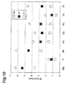
- Fig. 10 is a graph illustrating a sputtering yield of each of Ne, Ar, and Kr. Specifically, the graph illustrated in Fig. 10 shows a calculation result of efficiency, that is, a sputtering yield SY (atom/ion) by which each of Ne ions, Ar ions, and Kr ions having incidence energy of 3000 ev etches etching target layers formed from different metals.
- the sputtering yield SY is the number of metal atoms emitted from an etching target layer when one ion is incident on the etching target layer.
- the type of a metal atom is illustrated on a horizontal axis
- the sputtering yield SY is illustrated on a vertical axis.
- the Kr ion has a high sputtering yield SY, that is, high sputtering efficiency for a metal which may configure the etching target layer, for example, Pt, Mn, Mg, F, Co, Ru, or the like.
- the Kr ion has a sputtering yield SY of greater than or equal to 1 even for Ti or Ta which configures the mask. Therefore, the first process gas containing the first rare gas such as Kr enables a feature having high verticality to be formed in the etching target layer, and enables a large amount of the deposit to be removed.
- the first process gas has low selectivity with respect to the mask.
- the Ne ion has a sputtering yield SY which is low but greater than or equal to 1 for a metal which may configure the etching target layer, for example, Pt, Mn, Mg, F, Co, Ru, or the like.
- the Ne ion has a sputtering yield SY of less than 1 for Ti or Ta which may configure the mask. Therefore, the second process gas containing the second rare gas such as Ne has low etching efficiency for a metal which may configure the etching target layer, but enables the metal to be etched. In addition, the second process gas does not substantially etch the mask.
- the step of exposing the wafer to the plasma of the first process gas is able to improve the verticality of the feature formed by etching, and reduce the amount of the deposit on the side wall surface of the feature.
- the step of exposing the workpiece to the plasma of the second process gas is able to improve a selection ratio of the etching of the etching target layer with respect to the mask.
- the method MT by sequentially performing such two steps, it is possible to simultaneously satisfy three requirements, that is, (1) the high verticality of the feature formed by the etching, (2) the smallness of the amount of the deposit on the side wall surface of the feature, and (3) the high selection ratio of the etching of the etching target layer with respect to the mask.
- Fig. 2 is a diagram illustrating an example of the workpiece to which the method MT is applied.
- An example of the workpiece illustrated in Fig. 2 that is, a wafer W is a product which is obtained during the manufacturing of an MRAM element having an MTJ structure.
- the wafer W includes an underlying layer 100, an etching target layer 102, an MTJ structure 104, and an upper layer 106.
- the underlying layer 100 is a layer which will be a lower electrode and may be configured of Ta, and the thickness thereof is 3 nm.
- the etching target layer 102 is disposed on the underlying layer 100, and in an example, the etching target layer 102 is a layer which will be a pinning layer and is formed from PtMn, and the thickness thereof is 20 nm.
- the upper layer 106 is disposed on the etching target layer 102, and in an example, the upper layer 106 contains Ta. The thickness of the upper layer 106, for example, is 50 nm.
- the MTJ structure 104 is disposed between the etching target layer 102 and the upper layer 106, and is configured with multilayered films containing a metal such as a ferromagnetic material.
- the MTJ structure 104 is configured to have an insulating layer 104c between a first magnetic layer 104a and a second magnetic layer 104b.
- the first magnetic layer 104a and the second magnetic layer 104b are formed from CoFeB, and the thickness of each of the first magnetic layer 104a and the second magnetic layer 104b is 2.5 nm.
- the insulating layer 104c is a metal oxide layer such as an MgO layer, an aluminum oxide layer, a titanium oxide layer, or the like, and the thickness thereof is 1.2 nm.
- the wafer W may further include a magnetic layer 107 and a magnetic layer 108.
- the magnetic layer 107 is disposed on the etching target layer 102, and for example, may be formed from CoFe.
- the magnetic layer 108 is disposed between the magnetic layer 107 and the MTJ structure 104, and for example, is formed from Ru, and the thickness thereof is 0.8 nm.
- the etching target layer 102 of the wafer W is an example of an etching target of the method MT, and in one application example of the method MT, the etching target layer 102 is etched with a multilayer structure comprised of the upper layer 106, the MTJ structure 104, the magnetic layer 107, and the magnetic layer 108 serving as a mask MK.
- FIG. 3 is a diagram illustrating an example of a plasma processing apparatus.
- a plasma processing apparatus 10 illustrated in Fig. 3 is a capacitive coupling plasma processing apparatus. It should be noted that any plasma processing apparatus, such as an inductive coupling plasma processing apparatus or a plasma processing apparatus using a surface wave such as a microwave, may be used for performing the method MT.
- the plasma processing apparatus 10 includes a processing vessel 12.
- the processing vessel 12 has a substantially cylindrical shape, and defines a processing space S as an inner space thereof.
- the plasma processing apparatus 10 includes a base 14, which has a substantially disk shape, in the processing vessel 12.
- the base 14 is disposed below the processing space S.
- the base 14, for example, is formed of aluminum and configures the lower electrode.
- the base 14 has a function of absorbing the heat of an electrostatic chuck 50 described below and cooling the electrostatic chuck 50 in a process.
- a coolant flow passage 15 is formed in the base 14, and a coolant inlet pipe and a coolant outlet pipe are connected to the coolant flow passage 15.
- a suitable coolant for example, cooling water or the like is circulated in the coolant flow passage 15. Accordingly, the temperature of the base 14 and the electrostatic chuck 50 are controlled to a predetermined temperature.
- the plasma processing apparatus 10 further includes a cylindrical holding part 16 and a cylindrical supporting part 17.
- the cylindrical holding part 16 is in contact with the side surface and an edge portion of the bottom surface of the base 14 to hold the base 14.
- the cylindrical supporting part 17 extends to a vertical direction from a bottom portion of the processing vessel 12, and supports the base 14 through the cylindrical holding part 16.
- the plasma processing apparatus 10 further includes a focus ring 18 which is disposed on the upper surface of the cylindrical holding part 16.
- the focus ring 18 may be formed from, for example, silicon or quartz.
- an exhaust passage 20 is formed between the side wall of the processing vessel 12 and the cylindrical supporting part 17.
- a baffle plate 22 is attached to an inlet of the exhaust passage 20 or at the middle thereof.
- an exhaust port 24 is provided in a bottom portion of the exhaust passage 20.
- the exhaust port 24 is defined by an exhaust pipe 28 which is fitted into the bottom portion of the processing vessel 12.
- An exhaust device 26 is connected to the exhaust pipe 28.
- the exhaust device 26 includes a vacuum pump, and is able to depressurize the processing space S in the processing vessel 12 to a predetermined degree of vacuum.
- a gate valve 30, which opens and closes an opening for transferring the wafer W, is attached to the side wall of the processing vessel 12.
- a high frequency power source 32 for drawing ions is electrically connected to the base 14 through a matcher 34.
- the high frequency power source 32 applies high frequency bias power having a frequency suitable for drawing ions, for example, 400 KHz, to the lower electrode, that is, the base 14.
- the plasma processing apparatus 10 further includes a shower head 38.
- the shower head 38 is disposed above the processing space S.
- the shower head 38 includes an electrode plate 40 and an electrode support 42.
- the electrode plate 40 is a conductive plate having a substantially disk shape, and configures an upper electrode.
- a high frequency power source 35 for generating plasma is electrically connected to the electrode plate 40 through a matcher 36.
- the high frequency power source 35 supplies high frequency power having a frequency for generating plasma, for example, 60 MHz, to the electrode plate 40.
- high frequency power is applied to the electrode plate 40 by the high frequency power source 35, high frequency electric field is formed in a space between the base 14 and the electrode plate 40, that is, the processing space S.
- a plurality of gas flow holes 40h are formed in the electrode plate 40.
- the electrode plate 40 is detachably supported by the electrode support 42.
- a buffer chamber 42a is formed in the electrode support 42.
- the plasma processing apparatus 10 further includes a gas supply part 44, and the gas supply part 44 is connected to a gas introduction port 25 of the buffer chamber 42a through a gas supply conduit 46.
- the gas supply part 44 supplies a process gas to the processing space S.
- the gas supply part 44 is capable of supplying a plurality of types of gas. In one embodiment, the gas supply part 44 is capable of supplying methane gas, the first rare gas, the second rare gas, and hydrogen gas.
- a plurality of holes, which are continued to the respective gas flow holes 40h, are formed in the electrode support 42, and the plurality of holes are communicated with the buffer chamber 42a. Therefore, gas supplied from the gas supply part 44 is supplied to the processing space S through the buffer chamber 42a and the gas flow holes 40h.
- a magnetic field formation mechanism 48 which circularly or coaxially extends, is provided in a ceiling portion of the processing vessel 12 of the plasma processing apparatus 10.
- the magnetic field formation mechanism 48 functions such that high frequency discharge in the processing space S easily starts (plasma ignition), and the discharge is stably maintained.
- the electrostatic chuck 50 is disposed on the upper surface of the base 14.
- the electrostatic chuck 50 includes an electrode 52, and a pair of insulating films 54a and 54b.
- the insulating films 54a and 54b are films which are formed of an insulator such as ceramic.
- the electrode 52 is a conductive film, and is disposed between the insulating film 54a and the insulating film 54b.
- a direct current power source 56 is connected to the electrode 52 through a switch SW. When a direct current voltage is applied to the electrode 52 from the direct current power source 56, a coulomb force is generated, and the wafer W is attracted to and held on the electrostatic chuck 50 by the coulomb force.
- a heater which is a heating element, is embedded in the electrostatic chuck 50 to heat the wafer W to a predetermined temperature. The heater is connected to a heater power source through wiring.
- the plasma processing apparatus 10 further includes gas supply lines 58 and 60, and heat transfer gas supply parts 62 and 64.
- the heat transfer gas supply part 62 is connected to the gas supply line 58.
- the gas supply line 58 extends to the upper surface of the electrostatic chuck 50, and circularly extends in the center portion of the upper surface.
- the heat transfer gas supply part 62 supplies heat transfer gas such as He gas between the upper surface of the electrostatic chuck 50 and the wafer W.
- the heat transfer gas supply part 64 is connected to the gas supply line 60.
- the gas supply line 60 extends to the upper surface of the electrostatic chuck 50, and circularly extends in the upper surface such that the gas supply line 60 surrounds the gas supply line 58.
- the heat transfer gas supply part 64 supplies heat transfer gas such as He gas between the upper surface of the electrostatic chuck 50 and the wafer W.
- the plasma processing apparatus 10 further includes a controller 66.
- the controller 66 is connected to the exhaust device 26, the switch SW, the high frequency power source 32, the matcher 34, the high frequency power source 35, the matcher 36, the gas supply part 44, and the heat transfer gas supply parts 62 and 64.
- the controller 66 transmits control signals to the exhaust device 26, the switch SW, the high frequency power source 32, the matcher 34, the high frequency power source 35, the matcher 36, the gas supply part 44, and the heat transfer gas supply parts 62 and 64, respectively.
- the exhaustion of the exhaust device 26, the opening and closing of the switch SW, the supply of the high frequency bias power from the high frequency power source 32, the impedance adjustment of the matcher 34, the supply of the high frequency power from the high frequency power source 35, the impedance adjustment of the matcher 36, the supply of the process gas from the gas supply part 44, and the supply of the heat transfer gas from each of the heat transfer gas supply parts 62 and 64 are controlled by the control signals from the controller 66.
- the plasma processing apparatus 10 is capable of selectively supplying the first process gas and the second process gas to the processing space S from the gas supply part 44.
- a high frequency electric field is formed between the electrode plate 40 and the base 14, that is, in the processing space S, in a state where the process gas such as the first process gas and the second process gas is supplied to the processing space S, a plasma is generated in the processing space S.
- the etching target layer of the wafer W is etched by active species of elements contained in the process gas.
- the etching target layer 102 was a PtMn layer having a thickness of 20 nm.
- the upper layer 106 was a Ta layer, and the total thickness of the upper layer 106 and the MTJ structure 104 was approximately 50 nm.
- Fig. 4 is a graph illustrating etching efficiency of the etching target layer depending on a type of a rare gas.
- the etching efficiency of Fig. 4 was obtained by varying the rare gas in the process gas. Specifically, three types of gases, that is, argon (Ar) gas, Kr gas, and Ne gas were used as the rare gas. Other conditions at the time of obtaining the etching efficiency of Fig. 4 are as follows.
- etching efficiency is an etching rate with a process gas containing another rare gas in a case where an etching rate with a process gas containing Ar gas is set to "1".
- the process gas containing the Ar gas it is confirmed that in comparison with the process gas containing the Ar gas, the process gas containing the Kr gas has high etching efficiency for the etching target layer 102, whereas the etching gas containing the Ne gas has low etching efficiency for the etching target layer 102.
- Fig. 5A, Fig. 5B, and Fig. 5C are diagrams illustrating three graphs which show an influence of a type of a rare gas and an etching time with respect to the feature.
- Data shown in Fig. 5A, Fig. 5B, and Fig. 5C indicates etching time dependency of the feature obtained by etching the etching target layer 102 in the same conditions as those for obtaining the data of Fig. 4 .
- Fig. 5A a relationship between an etching time (a horizontal axis) and an angle ⁇ (a vertical axis) is illustrated.
- ⁇ a vertical axis
- a relationship between an etching time (a horizontal axis) and a thickness DA of a deposit (a vertical axis) is illustrated.
- a relationship between an etching time (a horizontal axis) and a thickness MH of the mask MK after being etched is illustrated.
- the angle ⁇ is an angle between the side wall surface of the etching target layer 102 after being etched and the undercoat layer.
- the thickness DA of the deposit is the thickness in a horizontal direction of the deposit DP remaining along the side wall surface of the mask MK after being etched.
- the thickness MH is the thickness in a film thickness direction of the mask MK remaining after being etched.
- the legend of "Ar gas” indicates data in a case of using the process gas containing Ar gas
- the legend of "Kr gas” indicates data in a case of using the process gas containing Kr gas
- the legend of "Ne gas” indicates data in a case of using the process gas containing Ar gas.
- an undercoat layer was exposed at an etching time of 60 seconds, an etching time of 40 seconds, and an etching time of 90 seconds in a case of using the process gas containing the Ar gas, a case of using the process gas containing the Kr gas, and a case of using the process gas containing the Ne gas, respectively. Therefore, etching over 60 seconds, etching over 40 seconds, and etching over 90 seconds are over-etching in a case of using the process gas containing the Ar gas, a case of using the process gas containing the Kr gas, and a case of using the process gas containing the Ne gas, respectively.
- the thickness DA of the deposit DP is large even when either the process gas containing the Ne gas or the process gas containing the Ar gas is used, whereas there is a tendency for the thickness DA of the deposit DP to decrease in proportion to the length of the etching time in a case where the process gas containing the Kr gas is used. Therefore, it is confirmed that it is possible to reduce the amount of the deposit by using the process gas containing the Kr gas as the rare gas.
- the thickness MH of the mask MK becomes small in a case where the process gas containing the Kr gas is used, whereas the thickness MH of the mask MK becomes large in a case where the process gas containing the Ne gas is used. Therefore, it is confirmed that in a case where the process gas containing the Ne gas is used, it is possible to maintain the film thickness of the mask MK, that is, it is possible to enhance selectivity of the etching target layer 102 with respect to the mask MK.
- Fig. 7A illustrates a sectional view of the state of the wafer after being etched in a case of using the process gas containing the Ar gas
- Fig. 7B illustrates a sectional view of the state of the wafer after being etched in a case of using the process gas containing the Ne gas
- Fig. 7C illustrates a sectional view of the state of the wafer after being etched in a case of using the process gas containing the Kr gas.
- using the process gas containing the Ne gas causes the verticality of the side wall of the etching target layer 102 to deteriorate and the amount of the deposit DP to increase, but enables the film thickness of the mask MK to be maintained, as illustrated in Fig. 7B . That is, it is possible to increase the selectivity of the etching target layer 102 with respect to the mask MK by using the process gas containing the Ne gas.
- Fig. 8A, Fig. 8B, and Fig. 8C are diagrams illustrating three graphs which show an influence of a type of a rare gas and a flow rate of methane gas with respect to the feature.
- Data shown in Fig. 8A, Fig. 8B, and Fig. 8C was obtained by changing the flow rate of the methane gas in the process gas on the basis of the conditions for obtaining the data of Fig. 4 .
- Fig. 8A a relationship between a percentage of the flow rate of the methane gas in the process gas (a horizontal axis) and the angle ⁇ (a vertical axis) is illustrated.
- a relationship between a percentage of the flow rate of the methane gas in the process gas (a horizontal axis) and the thickness DA of the deposit (a vertical axis) is illustrated.
- a relationship between a percentage of the flow rate of the methane gas in the process gas (a horizontal axis) and the thickness MH of the mask MK after being etched is illustrated.
- a legend of "Ar gas” indicates data in a case of using the process gas containing the Ar gas
- a legend of "Kr gas” indicates data in a case of using the process gas containing the Kr gas.
- Fig. 8A it is confirmed that in a case where the process gas containing the Ar gas is used, the verticality considerably deteriorates when the flow rate of the methane gas increases. In contrast, it is confirmed that the verticality is enhanced in proportion to the flow rate of the methane gas in a case where the process gas containing the Kr gas is used.
- Fig. 8B it is confirmed that in a case where the process gas containing the Kr gas is used, the amount of the deposit decreases even when the flow rate of the methane gas increases, in comparison with a case where the process gas containing the Ar gas is used,.
- Fig. 9A, Fig. 9B, and Fig. 9C are diagrams illustrating three graphs which show an influence of a type of a rare gas and high frequency bias power with respect to the feature. Data shown in Fig. 9A, Fig. 9B, and Fig. 9C was obtained by changing the high frequency bias power on the basis of the conditions for obtaining the data of Fig. 4 .
- Fig. 9A a relationship between the etching time (a horizontal axis) and the angle ⁇ (a vertical axis) is illustrated.
- Fig. 9A a relationship between the etching time (a horizontal axis) and the angle ⁇ (a vertical axis) is illustrated.
- Fig. 9A a relationship between the etching time (a horizontal axis) and the angle ⁇ (a vertical axis) is illustrated.
- Fig. 9A a relationship between the etching time (a horizontal axis) and the angle ⁇ (a vertical axis) is illustrated.
- a relationship between the etching time (a horizontal axis) and the thickness DA of the deposit (a vertical axis) is illustrated.
- a relationship between the etching time (a horizontal axis) and the thickness MH of the mask MK after being etched is illustrated.
- a legend of "Ar (1500 W)” indicates data in a case where the process gas containing the Ar gas was used and high frequency bias power of 1500 W was supplied
- a legend of "Kr (1500 W)” indicates data in a case where the process gas containing the Kr gas was used and high frequency bias power of 1500 W was supplied
- a legend of "Kr (1000 W)” indicates data in a case where the process gas containing the Kr gas was used and high frequency bias power of 1000 W was supplied.
- Fig. 9A it is confirmed that in a case where the process gas containing the Kr gas is used, it is possible to increase the angle ⁇ , that is, it is possible to improve the verticality, by increasing the high frequency bias power.
- low high frequency bias power 1000 W
- using the process gas containing the Kr gas makes it possible to obtain the same verticality as that in a case where the process gas containing the Ar gas is used and high frequency bias power (1500 W) is used.
- Fig. 9B it is confirmed that even when the high frequency bias power is low, it is possible to reduce the amount of the deposit by using the process gas containing the Kr gas, compared to a case where the process gas containing the Ar gas is used.
- Fig. 9C it is confirmed that even when the process gas containing the Kr gas is used, decreasing the high frequency bias power (1000 W) makes it possible to maintain the film thickness of the mask MK to the same level as that in a case where the process gas containing the Ar gas is used. That is, it is confirmed that even when the process gas containing the Kr gas is used, it is possible to realize the same selectivity as that in a case where the process gas containing the Ar gas is used.
- the first process gas containing the first rare gas such as Kr gas
- the first process gas containing the first rare gas it is possible to maintain the film thickness of the mask MK, that is, it is possible to obtain the selectivity to the same level as that in a case where the process gas containing the Ar gas is used.
- the second process gas containing the second rare gas such as Ne gas
- sequentially performing the step ST1 and the step ST2 are able to satisfy three requirements, that is, the improvement of the verticality, the smallness of the amount of the deposit, and the improvement of the selectivity.
- the method MT was applied to the same wafer as that at the time of obtaining the data of Fig. 4 , by using the plasma processing apparatus 10.
- the etching target layer 102 of the same wafer was etched by only using the process gas containing the Ar gas.
- the etching target layer 102 of the same wafer was etched by only using the process gas containing the Kr gas.
- the method MT it is possible to maintain the mask MK to have a thickness greater than that in a case where only the process gas containing the Kr gas is used (the second reference example) and to have the same thickness as that in a case where only the process gas containing the Ar gas is used (the first reference example), that is, it is possible to obtain the same selectivity as that in a case where only the process gas containing the Ar gas is used.
- the first process gas and the second process gas has been described to contain the methane gas and the hydrogen gas, but the first process gas and the second process gas may contain any gas insofar as the first process gas and the second process gas contain the first rare gas and the second rare gas, respectively, and contain carbon and hydrogen
- a layer formed from PtMn is exemplified as the etching target layer 102, but the etching target layer serving as the etching target of the method MT may be another layer which is able to be etched by using the upper layer 106 as a mask, for example, a layer included in the MTJ structure 104, the magnetic layer 107, and/or the magnetic layer 108.
Abstract
Description
- Embodiments of the present invention relates to a method for etching an etching target layer.
- A magnetic random access memory (MRAM) element having a magnetic tunnel junction (MTJ) structure has attracted attention as one type of a memory element using a magnetoresistance effect element.
- The MRAM element includes a multilayered film formed from a hard-to-etch material which contains a metal such as a ferromagnetic substance. In manufacturing of such an MRAM element, for example, a platinum manganese (PtMn) layer is etched by using a mask containing tantalum (Ta). In such etching, a halogen gas has been conventionally used, as disclosed in
Japanese Patent Application Laid-Open Publication No. 2012-204408 - [Patent Literature 1]
Japanese Patent Application Laid-Open Publication No. 2012-204408 - However, in etching using plasma of a halogen gas, a reaction product is deposited on the side wall surface of a feature formed by the etching. The reaction product has a high melting point, and thus, is not easily vaporized. In a case where such a deposit is deposited on the side wall surface of the MTJ structure of the MRAM element and is not removed, the function of the MRAM element is impaired.
- Therefore, in order to easily remove the reaction product in the following treatment step, the present inventors have made an attempt to use a process gas containing methane gas and argon gas as an etching gas.
- In contrast, in etching used in the manufacturing of the MRAM element, there are three requirements, that is, (1) high verticality of a feature formed by the etching, (2) smallness of an amount of a reaction product deposited on a side wall surface of the feature, that is, the smallness of an amount of a deposit, and (3) high selection ratio of the etching of an etching target layer with respect to a mask.
- In the etching in which a plasma of the process gas containing the methane gas and the argon gas is used, it is possible to improve the verticality and the selection ratio by increasing an amount of the methane gas. However, the amount of the deposit increases. In contrast, by reducing the amount of the methane gas, it is possible to reduce the amount of the deposit, but the verticality and the selection ratio deteriorates. Thus, the process gas containing the methane gas and the argon gas has a limit to simultaneously satisfy the three requirements.
- Therefore, as in the manufacture of the MRAM element, it is necessary to satisfy the three requirements described above in the etching of the etching target layer containing a metal.
- In one aspect, a method for etching an etching target layer of a workpiece is provided. The workpiece includes a mask on the etching target layer. The etching target layer and the mask are formed from respective materials for which etching efficiency by a plasma of a rare gas having an atomic number greater than an atomic number of argon is higher than etching efficiency for the materials by a plasma of argon gas. The mask is formed from a material having a melting point which is higher than a melting point of the etching target layer. The method includes a step (a) of exposing the workpiece to a plasma of a first process gas containing first rare gas having an atomic number greater than the atomic number of argon, and a step (b) of exposing the workpiece to a plasma of a second process gas containing a second rare gas having an atomic number less than the atomic number of argon. In one embodiment, the step (a) and the step (b) are alternately repeated.
- The plasma of the rare gas having an atomic number greater than the atomic number of the argon, that is, the plasma of the first rare gas has high sputtering efficiency, that is, high etching efficiency for a material having a relatively large atomic number. Therefore, the plasma of the first process gas containing the first rare gas is able to form a feature having high verticality and remove a large amount of a deposit, compared to the plasma of the process gas containing the argon gas. However, the plasma of the first process gas has low selectivity with respect to the mask. On the other hand, the plasma of the rare gas having an atomic number less than the atomic number of argon, that is, the plasma of the second rare gas has low sputtering efficiency, that is, low etching efficiency. Therefore, the plasma of the second process gas containing the second rare gas has low etching efficiency for a material having a large atomic number. However, the plasma of the second process gas has excellent selectivity with respect to the mask.
- The method is able to improve verticality of the feature formed by the etching in the step of exposing the workpiece to the plasma of the first process gas, and is able to reduce the deposit on the side wall surface of the feature. In addition, the method is able to improve a selection ratio of the etching of the etching target layer with respect to the mask by the step of exposing the workpiece to the plasma of the second process gas. By sequentially performing these two steps, the method is able to simultaneously satisfy the three requirements described above.
- An example of the etching target layer is a PtMn layer, and an example of the mask is a mask containing Ta. In addition, the first process gas and the second process gas may further contain methane gas.
- As described above, in etching of the etching target layer formed from the material having a relatively large atomic number such as a metal, it is possible to simultaneously satisfy the high verticality of the feature, the smallness of the amount of the deposit which is deposited on the side wall surface of the feature, and the high selection ratio of the etching of the etching target layer with respect the mask.
-
-
Fig. 1 is a flow chart illustrating an embodiment of a method of etching an etching target layer. -
Fig. 2 is a diagram illustrating an example of a workpiece to which a method MT is applied. -
Fig. 3 is a diagram illustrating an example of a plasma processing apparatus. -
Fig. 4 is a graph illustrating etching efficiency of the etching target layer according to a type of a rare gas. -
Fig. 5A, Fig. 5B, and Fig. 5C are diagrams illustrating three graphs which show an influence of a type of a rare gas and an etching time with respect to a feature. -
Fig. 6 is a diagram illustrating parameters of the feature. -
Fig. 7A, Fig. 7B, and Fig. 7C are diagrams illustrating a tendency of a type of a rare gas and a feature formed by etching. -
Fig. 8A, Fig. 8B, and Fig. 8C are diagrams illustrating three graphs which show an influence of a type of a rare gas and a flow rate of methane gas with respect to the feature. -
Fig. 9A, Fig. 9B, and Fig. 9C are diagrams illustrating three graphs which show an influence of a type of a rare gas and a high frequency bias power with respect to the feature. -
Fig. 10 is a graph illustrating a sputtering yield of each of Ne, Ar, and Kr. - Hereinafter, various embodiments will be described in detail with reference to the drawings. In the drawings, the same reference numerals are applied to the same or equivalent portions.
-
Fig. 1 is a flow chart illustrating an embodiment of a method for etching an etching target layer. A method MT illustrated inFig. 1 includes a step ST1 and a step ST2. In the step ST1, a workpiece (hereinafter, referred to as a "wafer") including an etching target layer is exposed to a plasma of a first process gas containing a first rare gas. In the step ST2, the wafer is exposed to a plasma of a second process gas containing a second rare gas. In one embodiment, alternative repetition of the step ST1 and the step ST2 may be performed. - The first rare gas contained in the first process gas is a rare gas having an atomic number which is greater than the atomic number of argon gas, and for example, is Kr gas. In addition, the second rare gas contained in the second process gas is a rare gas having an atomic number which is less than the atomic number of argon gas, and for example, is Ne gas. In addition, the first process gas and the second process gas may further contain methane gas and hydrogen gas.
- The wafer, which is an application target of the method MT, includes the etching target layer, and a mask provided on the etching target layer. The etching target layer and the mask are formed from respective materials for which etching efficiency by a plasma of a rare gas having an atomic number greater than the atomic number of argon is higher than etching efficiency for the materials by a plasma of argon gas. In addition, the mask is formed from a material having a melting point higher than the melting point of the etching target layer. The etching target layer and the mask may be formed from any such material. For example, the mask may include a film formed from TiN, Ta, Ti, TaN, or W. In addition, the etching target layer may be a layer formed from PtMn, IrMn, CoPd, CoPt, Ru, Mgo, CoFeB, CoFe, or Ni.
- In the method MT, the etching target layer is etched by the first process gas in the step ST1. The plasma of the rare gas having an atomic number greater than the atomic number of argon, that is, the plasma of the first rare gas has high sputtering efficiency, that is, high etching efficiency for a material having a relatively large atomic number. Therefore, the plasma of the first process gas containing the first rare gas is able to form a feature having high verticality and remove a large amount of a deposit, compared to a plasma of a process gas containing argon gas. However, the plasma of the first process gas has low selectivity with respect to the mask. In contrast, the plasma of the rare gas having an atomic number less than the atomic number of argon, that is, the plasma of the second rare gas has low sputtering efficiency, that is, low etching efficiency. Therefore, the plasma of the second process gas containing the second rare gas has low etching efficiency for a material having a large atomic number. However, the plasma of the second process gas has excellent selectivity with respect to the mask.
-
Fig. 10 is a graph illustrating a sputtering yield of each of Ne, Ar, and Kr. Specifically, the graph illustrated inFig. 10 shows a calculation result of efficiency, that is, a sputtering yield SY (atom/ion) by which each of Ne ions, Ar ions, and Kr ions having incidence energy of 3000 ev etches etching target layers formed from different metals. The sputtering yield SY is the number of metal atoms emitted from an etching target layer when one ion is incident on the etching target layer. InFig. 10 , the type of a metal atom is illustrated on a horizontal axis, and the sputtering yield SY is illustrated on a vertical axis. - As illustrated in
Fig. 10 , the Kr ion has a high sputtering yield SY, that is, high sputtering efficiency for a metal which may configure the etching target layer, for example, Pt, Mn, Mg, F, Co, Ru, or the like. However, the Kr ion has a sputtering yield SY of greater than or equal to 1 even for Ti or Ta which configures the mask. Therefore, the first process gas containing the first rare gas such as Kr enables a feature having high verticality to be formed in the etching target layer, and enables a large amount of the deposit to be removed. However, the first process gas has low selectivity with respect to the mask. - In contrast, the Ne ion has a sputtering yield SY which is low but greater than or equal to 1 for a metal which may configure the etching target layer, for example, Pt, Mn, Mg, F, Co, Ru, or the like. In addition, the Ne ion has a sputtering yield SY of less than 1 for Ti or Ta which may configure the mask. Therefore, the second process gas containing the second rare gas such as Ne has low etching efficiency for a metal which may configure the etching target layer, but enables the metal to be etched. In addition, the second process gas does not substantially etch the mask.
- As apparent from the graph illustrated in
Fig. 10 , in the method MT, the step of exposing the wafer to the plasma of the first process gas is able to improve the verticality of the feature formed by etching, and reduce the amount of the deposit on the side wall surface of the feature. In addition, the step of exposing the workpiece to the plasma of the second process gas is able to improve a selection ratio of the etching of the etching target layer with respect to the mask. Therefore, according to the method MT, by sequentially performing such two steps, it is possible to simultaneously satisfy three requirements, that is, (1) the high verticality of the feature formed by the etching, (2) the smallness of the amount of the deposit on the side wall surface of the feature, and (3) the high selection ratio of the etching of the etching target layer with respect to the mask. -
Fig. 2 is a diagram illustrating an example of the workpiece to which the method MT is applied. An example of the workpiece illustrated inFig. 2 , that is, a wafer W is a product which is obtained during the manufacturing of an MRAM element having an MTJ structure. As illustrated inFig. 2 , the wafer W includes anunderlying layer 100, anetching target layer 102, an MTJ structure 104, and anupper layer 106. In an example, theunderlying layer 100 is a layer which will be a lower electrode and may be configured of Ta, and the thickness thereof is 3 nm. Theetching target layer 102 is disposed on theunderlying layer 100, and in an example, theetching target layer 102 is a layer which will be a pinning layer and is formed from PtMn, and the thickness thereof is 20 nm. In addition, theupper layer 106 is disposed on theetching target layer 102, and in an example, theupper layer 106 contains Ta. The thickness of theupper layer 106, for example, is 50 nm. The MTJ structure 104 is disposed between theetching target layer 102 and theupper layer 106, and is configured with multilayered films containing a metal such as a ferromagnetic material. The MTJ structure 104, for example, is configured to have an insulating layer 104c between a firstmagnetic layer 104a and a second magnetic layer 104b. The firstmagnetic layer 104a and the second magnetic layer 104b, for example, are formed from CoFeB, and the thickness of each of the firstmagnetic layer 104a and the second magnetic layer 104b is 2.5 nm. The insulating layer 104c, for example, is a metal oxide layer such as an MgO layer, an aluminum oxide layer, a titanium oxide layer, or the like, and the thickness thereof is 1.2 nm. In addition, the wafer W may further include amagnetic layer 107 and amagnetic layer 108. Themagnetic layer 107 is disposed on theetching target layer 102, and for example, may be formed from CoFe. Themagnetic layer 108 is disposed between themagnetic layer 107 and the MTJ structure 104, and for example, is formed from Ru, and the thickness thereof is 0.8 nm. Theetching target layer 102 of the wafer W is an example of an etching target of the method MT, and in one application example of the method MT, theetching target layer 102 is etched with a multilayer structure comprised of theupper layer 106, the MTJ structure 104, themagnetic layer 107, and themagnetic layer 108 serving as a mask MK. - Hereinafter, a plasma processing apparatus which may be used for performing the method MT will be described.
Fig. 3 is a diagram illustrating an example of a plasma processing apparatus. Aplasma processing apparatus 10 illustrated inFig. 3 is a capacitive coupling plasma processing apparatus. It should be noted that any plasma processing apparatus, such as an inductive coupling plasma processing apparatus or a plasma processing apparatus using a surface wave such as a microwave, may be used for performing the method MT. - As illustrated in
Fig. 3 , theplasma processing apparatus 10 includes aprocessing vessel 12. Theprocessing vessel 12 has a substantially cylindrical shape, and defines a processing space S as an inner space thereof. Theplasma processing apparatus 10 includes abase 14, which has a substantially disk shape, in theprocessing vessel 12. Thebase 14 is disposed below the processing space S. Thebase 14, for example, is formed of aluminum and configures the lower electrode. Thebase 14 has a function of absorbing the heat of anelectrostatic chuck 50 described below and cooling theelectrostatic chuck 50 in a process. - A
coolant flow passage 15 is formed in thebase 14, and a coolant inlet pipe and a coolant outlet pipe are connected to thecoolant flow passage 15. In theplasma processing apparatus 10, a suitable coolant, for example, cooling water or the like is circulated in thecoolant flow passage 15. Accordingly, the temperature of thebase 14 and theelectrostatic chuck 50 are controlled to a predetermined temperature. - In addition, the
plasma processing apparatus 10 further includes a cylindrical holdingpart 16 and a cylindrical supportingpart 17. The cylindrical holdingpart 16 is in contact with the side surface and an edge portion of the bottom surface of the base 14 to hold thebase 14. The cylindrical supportingpart 17 extends to a vertical direction from a bottom portion of theprocessing vessel 12, and supports the base 14 through the cylindrical holdingpart 16. Theplasma processing apparatus 10 further includes afocus ring 18 which is disposed on the upper surface of the cylindrical holdingpart 16. Thefocus ring 18 may be formed from, for example, silicon or quartz. - In one embodiment, an
exhaust passage 20 is formed between the side wall of theprocessing vessel 12 and the cylindrical supportingpart 17. Abaffle plate 22 is attached to an inlet of theexhaust passage 20 or at the middle thereof. In addition, anexhaust port 24 is provided in a bottom portion of theexhaust passage 20. Theexhaust port 24 is defined by anexhaust pipe 28 which is fitted into the bottom portion of theprocessing vessel 12. Anexhaust device 26 is connected to theexhaust pipe 28. Theexhaust device 26 includes a vacuum pump, and is able to depressurize the processing space S in theprocessing vessel 12 to a predetermined degree of vacuum. Agate valve 30, which opens and closes an opening for transferring the wafer W, is attached to the side wall of theprocessing vessel 12. - A high
frequency power source 32 for drawing ions is electrically connected to the base 14 through amatcher 34. The highfrequency power source 32 applies high frequency bias power having a frequency suitable for drawing ions, for example, 400 KHz, to the lower electrode, that is, thebase 14. - The
plasma processing apparatus 10 further includes ashower head 38. Theshower head 38 is disposed above the processing space S. Theshower head 38 includes anelectrode plate 40 and anelectrode support 42. - The
electrode plate 40 is a conductive plate having a substantially disk shape, and configures an upper electrode. A highfrequency power source 35 for generating plasma is electrically connected to theelectrode plate 40 through amatcher 36. The highfrequency power source 35 supplies high frequency power having a frequency for generating plasma, for example, 60 MHz, to theelectrode plate 40. When the high frequency power is applied to theelectrode plate 40 by the highfrequency power source 35, high frequency electric field is formed in a space between the base 14 and theelectrode plate 40, that is, the processing space S. - A plurality of
gas flow holes 40h are formed in theelectrode plate 40. Theelectrode plate 40 is detachably supported by theelectrode support 42. Abuffer chamber 42a is formed in theelectrode support 42. Theplasma processing apparatus 10 further includes agas supply part 44, and thegas supply part 44 is connected to agas introduction port 25 of thebuffer chamber 42a through agas supply conduit 46. Thegas supply part 44 supplies a process gas to the processing space S. Thegas supply part 44 is capable of supplying a plurality of types of gas. In one embodiment, thegas supply part 44 is capable of supplying methane gas, the first rare gas, the second rare gas, and hydrogen gas. - A plurality of holes, which are continued to the respective
gas flow holes 40h, are formed in theelectrode support 42, and the plurality of holes are communicated with thebuffer chamber 42a. Therefore, gas supplied from thegas supply part 44 is supplied to the processing space S through thebuffer chamber 42a and thegas flow holes 40h. - In addition, a magnetic
field formation mechanism 48, which circularly or coaxially extends, is provided in a ceiling portion of theprocessing vessel 12 of theplasma processing apparatus 10. The magneticfield formation mechanism 48 functions such that high frequency discharge in the processing space S easily starts (plasma ignition), and the discharge is stably maintained. - In addition, the
electrostatic chuck 50 is disposed on the upper surface of thebase 14. Theelectrostatic chuck 50 includes anelectrode 52, and a pair of insulatingfilms films electrode 52 is a conductive film, and is disposed between the insulatingfilm 54a and the insulatingfilm 54b. A directcurrent power source 56 is connected to theelectrode 52 through a switch SW. When a direct current voltage is applied to theelectrode 52 from the directcurrent power source 56, a coulomb force is generated, and the wafer W is attracted to and held on theelectrostatic chuck 50 by the coulomb force. In addition, a heater, which is a heating element, is embedded in theelectrostatic chuck 50 to heat the wafer W to a predetermined temperature. The heater is connected to a heater power source through wiring. - The
plasma processing apparatus 10 further includesgas supply lines gas supply parts gas supply part 62 is connected to thegas supply line 58. Thegas supply line 58 extends to the upper surface of theelectrostatic chuck 50, and circularly extends in the center portion of the upper surface. The heat transfergas supply part 62 supplies heat transfer gas such as He gas between the upper surface of theelectrostatic chuck 50 and the wafer W. In addition, the heat transfergas supply part 64 is connected to thegas supply line 60. Thegas supply line 60 extends to the upper surface of theelectrostatic chuck 50, and circularly extends in the upper surface such that thegas supply line 60 surrounds thegas supply line 58. The heat transfergas supply part 64 supplies heat transfer gas such as He gas between the upper surface of theelectrostatic chuck 50 and the wafer W. - In addition, the
plasma processing apparatus 10 further includes acontroller 66. Thecontroller 66 is connected to theexhaust device 26, the switch SW, the highfrequency power source 32, thematcher 34, the highfrequency power source 35, thematcher 36, thegas supply part 44, and the heat transfergas supply parts controller 66 transmits control signals to theexhaust device 26, the switch SW, the highfrequency power source 32, thematcher 34, the highfrequency power source 35, thematcher 36, thegas supply part 44, and the heat transfergas supply parts exhaust device 26, the opening and closing of the switch SW, the supply of the high frequency bias power from the highfrequency power source 32, the impedance adjustment of thematcher 34, the supply of the high frequency power from the highfrequency power source 35, the impedance adjustment of thematcher 36, the supply of the process gas from thegas supply part 44, and the supply of the heat transfer gas from each of the heat transfergas supply parts controller 66. - The
plasma processing apparatus 10 is capable of selectively supplying the first process gas and the second process gas to the processing space S from thegas supply part 44. When a high frequency electric field is formed between theelectrode plate 40 and thebase 14, that is, in the processing space S, in a state where the process gas such as the first process gas and the second process gas is supplied to the processing space S, a plasma is generated in the processing space S. The etching target layer of the wafer W is etched by active species of elements contained in the process gas. - Hereinafter, effectiveness of the method MT will be described by showing various data items. The following data items were obtained by etching the wafer W illustrated in
Fig. 2 using theplasma processing apparatus 10. Theetching target layer 102 was a PtMn layer having a thickness of 20 nm. In addition, theupper layer 106 was a Ta layer, and the total thickness of theupper layer 106 and the MTJ structure 104 was approximately 50 nm. - Reference is made to
Fig. 4. Fig. 4 is a graph illustrating etching efficiency of the etching target layer depending on a type of a rare gas. The etching efficiency ofFig. 4 was obtained by varying the rare gas in the process gas. Specifically, three types of gases, that is, argon (Ar) gas, Kr gas, and Ne gas were used as the rare gas. Other conditions at the time of obtaining the etching efficiency ofFig. 4 are as follows. -
- Pressure in Processing vessel 12: 10 mTorr (1.333 Pa)
- High Frequency Power for Generating Plasma: 800 W
- High Frequency Bias Power: 1500 W
- Flow Rate of Hydrogen Gas in Process gas: 300 sccm
- Flow Rate of Methane Gas in Process gas: 90 sccm
- Flow Rate of Rare Gas in Process gas: 50 sccm
- Wafer Temperature: -20°C
- In
Fig. 4 , the type of a rare gas in the process gas is illustrated on a horizontal axis, and etching efficiency is illustrated on a vertical axis. The etching efficiency is an etching rate with a process gas containing another rare gas in a case where an etching rate with a process gas containing Ar gas is set to "1". Referring toFig. 4 , it is confirmed that in comparison with the process gas containing the Ar gas, the process gas containing the Kr gas has high etching efficiency for theetching target layer 102, whereas the etching gas containing the Ne gas has low etching efficiency for theetching target layer 102. - Reference is made to
Fig. 5A, Fig. 5B, and Fig. 5C. Fig. 5A, Fig. 5B, and Fig. 5C are diagrams illustrating three graphs which show an influence of a type of a rare gas and an etching time with respect to the feature. Data shown inFig. 5A, Fig. 5B, and Fig. 5C indicates etching time dependency of the feature obtained by etching theetching target layer 102 in the same conditions as those for obtaining the data ofFig. 4 . Specifically, inFig. 5A , a relationship between an etching time (a horizontal axis) and an angle θ (a vertical axis) is illustrated. In addition, inFig. 5B , a relationship between an etching time (a horizontal axis) and a thickness DA of a deposit (a vertical axis) is illustrated. Further, inFig. 5C , a relationship between an etching time (a horizontal axis) and a thickness MH of the mask MK after being etched is illustrated. As illustrated inFig. 6 , the angle θ is an angle between the side wall surface of theetching target layer 102 after being etched and the undercoat layer. In addition, the thickness DA of the deposit is the thickness in a horizontal direction of the deposit DP remaining along the side wall surface of the mask MK after being etched. Further, the thickness MH is the thickness in a film thickness direction of the mask MK remaining after being etched. InFig. 5A, Fig. 5B, and Fig. 5C , the legend of "Ar gas" indicates data in a case of using the process gas containing Ar gas, the legend of "Kr gas" indicates data in a case of using the process gas containing Kr gas, and the legend of "Ne gas" indicates data in a case of using the process gas containing Ar gas. - In the experiment for obtaining the data of
Fig. 5A, Fig. 5B, and Fig. 5C , an undercoat layer was exposed at an etching time of 60 seconds, an etching time of 40 seconds, and an etching time of 90 seconds in a case of using the process gas containing the Ar gas, a case of using the process gas containing the Kr gas, and a case of using the process gas containing the Ne gas, respectively. Therefore, etching over 60 seconds, etching over 40 seconds, and etching over 90 seconds are over-etching in a case of using the process gas containing the Ar gas, a case of using the process gas containing the Kr gas, and a case of using the process gas containing the Ne gas, respectively. - Referring to
Fig. 5A , it is confirmed that there is a limit to improve the angle θ even when either the process gas containing the Ne gas or the process gas containing the Ar gas is used, whereas there is a tendency for the angle θ to be close to 90 degrees in proportion to the length of the etching time in a case where the process gas containing the Kr gas is used. Therefore, it is confirmed that the verticality of the feature formed by the etching is enhanced by using the process gas containing the Kr gas as the rare gas. In addition, it is confirmed that by using the process gas containing the Kr gas, it is possible to obtain an angle, that is, the verticality which is not able to be obtained by the process gas containing the Ar gas. - Referring to
Fig. 5B , it is confirmed that the thickness DA of the deposit DP is large even when either the process gas containing the Ne gas or the process gas containing the Ar gas is used, whereas there is a tendency for the thickness DA of the deposit DP to decrease in proportion to the length of the etching time in a case where the process gas containing the Kr gas is used. Therefore, it is confirmed that it is possible to reduce the amount of the deposit by using the process gas containing the Kr gas as the rare gas. - Referring to
Fig. 5C , it is confirmed that the thickness MH of the mask MK becomes small in a case where the process gas containing the Kr gas is used, whereas the thickness MH of the mask MK becomes large in a case where the process gas containing the Ne gas is used. Therefore, it is confirmed that in a case where the process gas containing the Ne gas is used, it is possible to maintain the film thickness of the mask MK, that is, it is possible to enhance selectivity of theetching target layer 102 with respect to the mask MK. - The tendency confirmed from the data of
Fig. 4 ,Fig. 5A, Fig. 5B, and Fig. 5C will be described with reference toFig. 7A, Fig. 7B, and Fig. 7C. Fig. 7A illustrates a sectional view of the state of the wafer after being etched in a case of using the process gas containing the Ar gas,Fig. 7B illustrates a sectional view of the state of the wafer after being etched in a case of using the process gas containing the Ne gas, andFig. 7C illustrates a sectional view of the state of the wafer after being etched in a case of using the process gas containing the Kr gas. - In comparison with the tendency (see
Fig. 7A ) of the case using the process gas containing the Ar gas, it is possible to enhance the verticality of the side wall of theetching target layer 102 and to reduce the amount of the deposit DP by using the process gas containing the Kr gas, as illustrated inFig. 7C . However, in a case where the process gas containing the Kr gas is used, the film thickness of the mask MK decreases, and the shoulder of the mask MK is largely removed. In addition, in comparison with the tendency of the case using the process gas containing the Ar gas, using the process gas containing the Ne gas causes the verticality of the side wall of theetching target layer 102 to deteriorate and the amount of the deposit DP to increase, but enables the film thickness of the mask MK to be maintained, as illustrated inFig. 7B . That is, it is possible to increase the selectivity of theetching target layer 102 with respect to the mask MK by using the process gas containing the Ne gas. - Reference is made to
Fig. 8A, Fig. 8B, and Fig. 8C. Fig. 8A, Fig. 8B, and Fig. 8C are diagrams illustrating three graphs which show an influence of a type of a rare gas and a flow rate of methane gas with respect to the feature. Data shown inFig. 8A, Fig. 8B, and Fig. 8C was obtained by changing the flow rate of the methane gas in the process gas on the basis of the conditions for obtaining the data ofFig. 4 . Specifically, inFig. 8A , a relationship between a percentage of the flow rate of the methane gas in the process gas (a horizontal axis) and the angle θ (a vertical axis) is illustrated. In addition, inFig. 8B , a relationship between a percentage of the flow rate of the methane gas in the process gas (a horizontal axis) and the thickness DA of the deposit (a vertical axis) is illustrated. In addition, inFig. 8C , a relationship between a percentage of the flow rate of the methane gas in the process gas (a horizontal axis) and the thickness MH of the mask MK after being etched is illustrated. InFig. 8A, Fig. 8B, and Fig. 8C , a legend of "Ar gas" indicates data in a case of using the process gas containing the Ar gas, and a legend of "Kr gas" indicates data in a case of using the process gas containing the Kr gas. - Referring to
Fig. 8A , it is confirmed that in a case where the process gas containing the Ar gas is used, the verticality considerably deteriorates when the flow rate of the methane gas increases. In contrast, it is confirmed that the verticality is enhanced in proportion to the flow rate of the methane gas in a case where the process gas containing the Kr gas is used. Referring toFig. 8B , it is confirmed that in a case where the process gas containing the Kr gas is used, the amount of the deposit decreases even when the flow rate of the methane gas increases, in comparison with a case where the process gas containing the Ar gas is used,. Referring toFig. 8C , it is confirmed that in a case where the process gas containing the Kr gas is used, increasing the flow rate of the methane gas enables the thickness of the mask MK after being etched to be maintained to the same level as that in a case where the process gas containing the Ar gas is used. Therefore, it is confirmed that according to the process gas containing the Kr gas, it is possible to improve the verticality, to reduce the amount of the deposit, and to obtain the same selectivity as that in a case where the process gas containing the Ar gas, by adjusting the amount of methane gas. - Reference is made to
Fig. 9A, Fig. 9B, and Fig. 9C. Fig. 9A, Fig. 9B, and Fig. 9C are diagrams illustrating three graphs which show an influence of a type of a rare gas and high frequency bias power with respect to the feature. Data shown inFig. 9A, Fig. 9B, and Fig. 9C was obtained by changing the high frequency bias power on the basis of the conditions for obtaining the data ofFig. 4 . InFig. 9A , a relationship between the etching time (a horizontal axis) and the angle θ (a vertical axis) is illustrated. In addition, inFig. 9B , a relationship between the etching time (a horizontal axis) and the thickness DA of the deposit (a vertical axis) is illustrated. In addition, inFig. 9C , a relationship between the etching time (a horizontal axis) and the thickness MH of the mask MK after being etched is illustrated. InFig. 9A, Fig. 9B, and Fig. 9C , a legend of "Ar (1500 W)" indicates data in a case where the process gas containing the Ar gas was used and high frequency bias power of 1500 W was supplied, a legend of "Kr (1500 W)" indicates data in a case where the process gas containing the Kr gas was used and high frequency bias power of 1500 W was supplied, and a legend of "Kr (1000 W)" indicates data in a case where the process gas containing the Kr gas was used and high frequency bias power of 1000 W was supplied. - Referring to
Fig. 9A , it is confirmed that in a case where the process gas containing the Kr gas is used, it is possible to increase the angle θ, that is, it is possible to improve the verticality, by increasing the high frequency bias power. In addition, it is confirmed that in comparison with a case where the process gas containing the Ar gas is used, it is possible to obtain high verticality by using the process gas containing the Kr gas even with the same high frequency bias power. Further, it is confirmed that even when low high frequency bias power (1000 W) is used, using the process gas containing the Kr gas makes it possible to obtain the same verticality as that in a case where the process gas containing the Ar gas is used and high frequency bias power (1500 W) is used. - Referring to
Fig. 9B , it is confirmed that even when the high frequency bias power is low, it is possible to reduce the amount of the deposit by using the process gas containing the Kr gas, compared to a case where the process gas containing the Ar gas is used. Referring toFig. 9C , it is confirmed that even when the process gas containing the Kr gas is used, decreasing the high frequency bias power (1000 W) makes it possible to maintain the film thickness of the mask MK to the same level as that in a case where the process gas containing the Ar gas is used. That is, it is confirmed that even when the process gas containing the Kr gas is used, it is possible to realize the same selectivity as that in a case where the process gas containing the Ar gas is used. - To sum up the confirmed matters from the data items described above, it is possible to improve the verticality and reduce the amount of the deposit by using the first process gas containing the first rare gas such as Kr gas, compared to the process gas containing the Ar gas. In addition, by using the first process gas containing the first rare gas, it is possible to maintain the film thickness of the mask MK, that is, it is possible to obtain the selectivity to the same level as that in a case where the process gas containing the Ar gas is used. In addition, it is possible to improve the selectivity by using the second process gas containing the second rare gas such as Ne gas, compared to a case where the process gas containing the Kr gas or the Ar gas is used. Therefore, sequentially performing the step ST1 and the step ST2 are able to satisfy three requirements, that is, the improvement of the verticality, the smallness of the amount of the deposit, and the improvement of the selectivity.
- Hereinafter, an experimental example in which the method MT was performed will be described. In the experimental example, the method MT was applied to the same wafer as that at the time of obtaining the data of
Fig. 4 , by using theplasma processing apparatus 10. In addition, as a first reference example, theetching target layer 102 of the same wafer was etched by only using the process gas containing the Ar gas. Further, as a second reference example, theetching target layer 102 of the same wafer was etched by only using the process gas containing the Kr gas. Hereinafter, conditions of the experimental example, the first reference example, and the second reference example will be described. -
- Pressure in Processing vessel 12: 10 mTorr (1.333 Pa)
- High Frequency Power for Generating Plasma: 800 W
- High Frequency Bias Power: 1500 W
- Flow Rate of Hydrogen Gas in First Process gas and Second Process gas: 300 sccm
- Flow Rate of Methane Gas in First Process gas and Second Process gas: 90 sccm
- Flow Rate of Rare Gas in First Process gas and Second Process gas: 50 sccm
- First Rare Gas: Kr
- Second Rare Gas: Ne
- Wafer Temperature: -20°C
- Time of Step ST1: 10 seconds
- Time of Step ST2: 10 seconds
- Number of Repetitions of Sequence Including Step ST1 and Step ST2: 5 times
-
- Pressure in Processing vessel 12: 10 mTorr (1.333 Pa)
- High Frequency Power for Generating Plasma: 800 W
- High Frequency Bias Power: 1500 W
- Flow Rate of Hydrogen Gas in Process gas: 300 sccm
- Flow Rate of Methane Gas in Process gas: 90 sccm
- Flow Rate of Ar Gas in Process gas: 50 sccm
- Wafer Temperature: -20°C
- Etching Time: 130 seconds
-
- Pressure in Processing vessel 12: 10 mTorr (1.333 Pa)
- High Frequency Power for Generating Plasma: 800 W
- High Frequency Bias Power: 1500 W
- Flow Rate of Hydrogen Gas in Process gas: 300 sccm
- Flow Rate of Methane Gas in Process gas: 90 sccm
- Flow Rate of Kr Gas in Process gas: 50 sccm
- Wafer Temperature: -20°C
- Etching Time: 130 seconds
- Hereinafter, in each of the experimental example, the first reference example, and the second reference example, the angle θ after being etched, the thickness DA of the deposit DP, and the thickness MH of the mask MK after being etched will be described.
-
- θ: 83 degrees
- DA: 1.5 nm
- MH: 35.1 nm
-
- θ: 81.5 degrees
- DA: 4.0 nm
- MH: 36.0 nm
-
- θ: 84 degrees
- DA: 0 nm
- MH: 24.2 nm
- As it is apparent by comparing the angles θ after being etched, the thicknesses DA of the deposit, and the thicknesses MH of the mask MK after being etched of the experimental example, the first reference example, and the second reference example to each other, it is confirmed that according to the method MT, it is possible to realize verticality having a level which is not able to be obtained in a case where only the process gas containing the Ar gas is used (the first reference example), and it is possible to reduce the amount of deposit. In addition, it is confirmed that according to the method MT, it is possible to maintain the mask MK to have a thickness greater than that in a case where only the process gas containing the Kr gas is used (the second reference example) and to have the same thickness as that in a case where only the process gas containing the Ar gas is used (the first reference example), that is, it is possible to obtain the same selectivity as that in a case where only the process gas containing the Ar gas is used.
- As described above, various embodiments have been described, but various modifications may be made without being limited to the embodiment described above. For example, the first process gas and the second process gas has been described to contain the methane gas and the hydrogen gas, but the first process gas and the second process gas may contain any gas insofar as the first process gas and the second process gas contain the first rare gas and the second rare gas, respectively, and contain carbon and hydrogen In addition, in the embodiments described above, a layer formed from PtMn is exemplified as the
etching target layer 102, but the etching target layer serving as the etching target of the method MT may be another layer which is able to be etched by using theupper layer 106 as a mask, for example, a layer included in the MTJ structure 104, themagnetic layer 107, and/or themagnetic layer 108. -
- 10: plasma processing apparatus
- 12: processing vessel
- 32: high frequency power source (for supplying high frequency bias power)
- W: wafer
- 100: underlying layer
- 102: etching target layer
- 104: MTJ structure
- 106: upper layer
- MK: mask
- DP: deposit
- MT: method
- ST1: step
- ST2: step
Claims (4)
- A method for etching an etching target layer of a workpiece, whereinthe workpiece includes a mask on the etching target layer,the etching target layer and the mask are formed from respective materials for which etching efficiency of a plasma of a rare gas having an atomic number greater than an atomic number of argon is higher than etching efficiency for the materials by a plasma of an argon gas, andthe mask is formed from a material having a melting point which is higher than a melting point of the etching target layer,the method comprising:exposing the workpiece to a plasma of a first process gas containing a first rare gas having an atomic number greater than an atomic number of argon; andexposing the workpiece to a plasma of a second process gas containing a second rare gas having an atomic number less than the atomic number of argon.
- The method according to claim 1, wherein said exposing the workpiece to the plasma of the first process gas and said exposing the workpiece to the plasma of the second process gas are alternately repeated.
- The method according to claim 1 or 2,wherein the etching target layer contains PtMn, andthe mask contains Ta.
- The method according to any one of claims 1 to 3,wherein the first process gas and the second process gas further contain methane gas.
Applications Claiming Priority (3)
| Application Number | Priority Date | Filing Date | Title |
|---|---|---|---|
| JP2013239908 | 2013-11-20 | ||
| JP2014170521A JP6347695B2 (en) | 2013-11-20 | 2014-08-25 | Method for etching a layer to be etched |
| PCT/JP2014/074922 WO2015076010A1 (en) | 2013-11-20 | 2014-09-19 | Method for etching layer to be etched. |
Publications (3)
| Publication Number | Publication Date |
|---|---|
| EP3073518A1 true EP3073518A1 (en) | 2016-09-28 |
| EP3073518A4 EP3073518A4 (en) | 2017-07-19 |
| EP3073518B1 EP3073518B1 (en) | 2018-03-07 |
Family
ID=53179281
Family Applications (1)
| Application Number | Title | Priority Date | Filing Date |
|---|---|---|---|
| EP14863512.1A Active EP3073518B1 (en) | 2013-11-20 | 2014-09-19 | Method for etching layer to be etched. |
Country Status (6)
| Country | Link |
|---|---|
| US (1) | US9647206B2 (en) |
| EP (1) | EP3073518B1 (en) |
| JP (1) | JP6347695B2 (en) |
| KR (1) | KR102257855B1 (en) |
| TW (1) | TWI629724B (en) |
| WO (1) | WO2015076010A1 (en) |
Families Citing this family (8)
| Publication number | Priority date | Publication date | Assignee | Title |
|---|---|---|---|---|
| US9768033B2 (en) * | 2014-07-10 | 2017-09-19 | Tokyo Electron Limited | Methods for high precision etching of substrates |
| US9870899B2 (en) | 2015-04-24 | 2018-01-16 | Lam Research Corporation | Cobalt etch back |
| US9972504B2 (en) | 2015-08-07 | 2018-05-15 | Lam Research Corporation | Atomic layer etching of tungsten for enhanced tungsten deposition fill |
| US10566212B2 (en) * | 2016-12-19 | 2020-02-18 | Lam Research Corporation | Designer atomic layer etching |
| JP6552477B2 (en) * | 2016-12-22 | 2019-07-31 | 東京エレクトロン株式会社 | Etching method |
| US10832909B2 (en) | 2017-04-24 | 2020-11-10 | Lam Research Corporation | Atomic layer etch, reactive precursors and energetic sources for patterning applications |
| US10796912B2 (en) | 2017-05-16 | 2020-10-06 | Lam Research Corporation | Eliminating yield impact of stochastics in lithography |
| KR102642011B1 (en) | 2018-03-30 | 2024-02-27 | 램 리써치 코포레이션 | Atomic layer etching and smoothing of refractory metals and other high surface binding energy materials |
Family Cites Families (15)
| Publication number | Priority date | Publication date | Assignee | Title |
|---|---|---|---|---|
| JPH03165027A (en) * | 1989-11-22 | 1991-07-17 | Nec Corp | Reactive ion etching |
| JP3440735B2 (en) * | 1996-12-26 | 2003-08-25 | ソニー株式会社 | Dry etching method |
| US6544429B1 (en) * | 1999-03-25 | 2003-04-08 | Applied Materials Inc. | Enhancement of silicon oxide etch rate and substrate selectivity with xenon addition |
| JP2002163848A (en) * | 2000-11-27 | 2002-06-07 | Canon Inc | Manufacturing method of information recording medium |
| JP2004031466A (en) * | 2002-06-24 | 2004-01-29 | Hitachi High-Technologies Corp | Plasma treatment method |
| US7645618B2 (en) * | 2004-09-09 | 2010-01-12 | Tegal Corporation | Dry etch stop process for eliminating electrical shorting in MRAM device structures |
| US8278222B2 (en) * | 2005-11-22 | 2012-10-02 | Air Products And Chemicals, Inc. | Selective etching and formation of xenon difluoride |
| US7608195B2 (en) * | 2006-02-21 | 2009-10-27 | Micron Technology, Inc. | High aspect ratio contacts |
| KR20100005058A (en) * | 2007-03-30 | 2010-01-13 | 캐논 아네르바 가부시키가이샤 | Method of fabricating magnetic device |
| US8282844B2 (en) * | 2007-08-01 | 2012-10-09 | Tokyo Electron Limited | Method for etching metal nitride with high selectivity to other materials |
| US20100301008A1 (en) * | 2009-05-27 | 2010-12-02 | Canon Anelva Corporation | Process and apparatus for fabricating magnetic device |
| US20100304504A1 (en) * | 2009-05-27 | 2010-12-02 | Canon Anelva Corporation | Process and apparatus for fabricating magnetic device |
| JP2012204408A (en) | 2011-03-23 | 2012-10-22 | Toshiba Corp | Manufacturing method of semiconductor device |
| JP2012222093A (en) * | 2011-04-07 | 2012-11-12 | Ulvac Japan Ltd | Manufacturing method and manufacturing apparatus of magnetoresistive element |
| US8546263B2 (en) * | 2011-04-27 | 2013-10-01 | Applied Materials, Inc. | Method of patterning of magnetic tunnel junctions |
-
2014
- 2014-08-25 JP JP2014170521A patent/JP6347695B2/en active Active
- 2014-09-19 US US15/030,406 patent/US9647206B2/en active Active
- 2014-09-19 WO PCT/JP2014/074922 patent/WO2015076010A1/en active Application Filing
- 2014-09-19 KR KR1020167008370A patent/KR102257855B1/en active IP Right Grant
- 2014-09-19 EP EP14863512.1A patent/EP3073518B1/en active Active
- 2014-11-06 TW TW103138614A patent/TWI629724B/en active
Also Published As
| Publication number | Publication date |
|---|---|
| US9647206B2 (en) | 2017-05-09 |
| TW201532138A (en) | 2015-08-16 |
| JP6347695B2 (en) | 2018-06-27 |
| JP2015122473A (en) | 2015-07-02 |
| TWI629724B (en) | 2018-07-11 |
| KR20160088855A (en) | 2016-07-26 |
| US20160276582A1 (en) | 2016-09-22 |
| EP3073518B1 (en) | 2018-03-07 |
| KR102257855B1 (en) | 2021-05-28 |
| EP3073518A4 (en) | 2017-07-19 |
| WO2015076010A1 (en) | 2015-05-28 |
Similar Documents
| Publication | Publication Date | Title |
|---|---|---|
| EP3073518B1 (en) | Method for etching layer to be etched. | |
| US10217933B2 (en) | Method for etching multilayer film | |
| JP6373160B2 (en) | Plasma processing equipment | |
| TWI597785B (en) | Plasma processing method and plasma processing device | |
| US9793130B2 (en) | Method for processing object to be processed | |
| TWI591722B (en) | Etching method of film containing cobalt and palladium | |
| KR20140056051A (en) | Etching method and substrate processing apparatus | |
| JP6096762B2 (en) | Plasma processing method and plasma processing apparatus | |
| KR102365473B1 (en) | Method for etching object to be processed | |
| CN107710391B (en) | Method for etching multilayer film | |
| TW201923895A (en) | Method for etching |
Legal Events
| Date | Code | Title | Description |
|---|---|---|---|
| PUAI | Public reference made under article 153(3) epc to a published international application that has entered the european phase |
Free format text: ORIGINAL CODE: 0009012 |
|
| 17P | Request for examination filed |
Effective date: 20160414 |
|
| AK | Designated contracting states |
Kind code of ref document: A1 Designated state(s): AL AT BE BG CH CY CZ DE DK EE ES FI FR GB GR HR HU IE IS IT LI LT LU LV MC MK MT NL NO PL PT RO RS SE SI SK SM TR |
|
| AX | Request for extension of the european patent |
Extension state: BA ME |
|
| DAX | Request for extension of the european patent (deleted) | ||
| A4 | Supplementary search report drawn up and despatched |
Effective date: 20170619 |
|
| RIC1 | Information provided on ipc code assigned before grant |
Ipc: H01L 43/08 20060101AFI20170612BHEP Ipc: H01L 43/12 20060101ALI20170612BHEP |
|
| REG | Reference to a national code |
Ref country code: DE Ref legal event code: R079 Ref document number: 602014022209 Country of ref document: DE Free format text: PREVIOUS MAIN CLASS: H01L0021306500 Ipc: H01L0043080000 |
|
| RIN1 | Information on inventor provided before grant (corrected) |
Inventor name: HASHIMOTO, MITSURU Inventor name: SHIMODA, KEIICHI Inventor name: NISHIMURA, EIICHI Inventor name: SONE, TAKASHI |
|
| GRAP | Despatch of communication of intention to grant a patent |
Free format text: ORIGINAL CODE: EPIDOSNIGR1 |
|
| STAA | Information on the status of an ep patent application or granted ep patent |
Free format text: STATUS: GRANT OF PATENT IS INTENDED |
|
| RIC1 | Information provided on ipc code assigned before grant |
Ipc: H01L 43/08 20060101AFI20170811BHEP Ipc: H01L 43/12 20060101ALI20170811BHEP |
|
| INTG | Intention to grant announced |
Effective date: 20170919 |
|
| GRAS | Grant fee paid |
Free format text: ORIGINAL CODE: EPIDOSNIGR3 |
|
| GRAA | (expected) grant |
Free format text: ORIGINAL CODE: 0009210 |
|
| STAA | Information on the status of an ep patent application or granted ep patent |
Free format text: STATUS: THE PATENT HAS BEEN GRANTED |
|
| AK | Designated contracting states |
Kind code of ref document: B1 Designated state(s): AL AT BE BG CH CY CZ DE DK EE ES FI FR GB GR HR HU IE IS IT LI LT LU LV MC MK MT NL NO PL PT RO RS SE SI SK SM TR |
|
| REG | Reference to a national code |
Ref country code: GB Ref legal event code: FG4D |
|
| REG | Reference to a national code |
Ref country code: CH Ref legal event code: EP Ref country code: AT Ref legal event code: REF Ref document number: 977441 Country of ref document: AT Kind code of ref document: T Effective date: 20180315 |
|
| REG | Reference to a national code |
Ref country code: IE Ref legal event code: FG4D |
|
| REG | Reference to a national code |
Ref country code: DE Ref legal event code: R096 Ref document number: 602014022209 Country of ref document: DE |
|
| REG | Reference to a national code |
Ref country code: NL Ref legal event code: MP Effective date: 20180307 |
|
| REG | Reference to a national code |
Ref country code: LT Ref legal event code: MG4D |
|
| PG25 | Lapsed in a contracting state [announced via postgrant information from national office to epo] |
Ref country code: LT Free format text: LAPSE BECAUSE OF FAILURE TO SUBMIT A TRANSLATION OF THE DESCRIPTION OR TO PAY THE FEE WITHIN THE PRESCRIBED TIME-LIMIT Effective date: 20180307 Ref country code: CY Free format text: LAPSE BECAUSE OF FAILURE TO SUBMIT A TRANSLATION OF THE DESCRIPTION OR TO PAY THE FEE WITHIN THE PRESCRIBED TIME-LIMIT Effective date: 20180307 Ref country code: NO Free format text: LAPSE BECAUSE OF FAILURE TO SUBMIT A TRANSLATION OF THE DESCRIPTION OR TO PAY THE FEE WITHIN THE PRESCRIBED TIME-LIMIT Effective date: 20180607 Ref country code: FI Free format text: LAPSE BECAUSE OF FAILURE TO SUBMIT A TRANSLATION OF THE DESCRIPTION OR TO PAY THE FEE WITHIN THE PRESCRIBED TIME-LIMIT Effective date: 20180307 Ref country code: HR Free format text: LAPSE BECAUSE OF FAILURE TO SUBMIT A TRANSLATION OF THE DESCRIPTION OR TO PAY THE FEE WITHIN THE PRESCRIBED TIME-LIMIT Effective date: 20180307 Ref country code: ES Free format text: LAPSE BECAUSE OF FAILURE TO SUBMIT A TRANSLATION OF THE DESCRIPTION OR TO PAY THE FEE WITHIN THE PRESCRIBED TIME-LIMIT Effective date: 20180307 |
|
| REG | Reference to a national code |
Ref country code: AT Ref legal event code: MK05 Ref document number: 977441 Country of ref document: AT Kind code of ref document: T Effective date: 20180307 |
|
| PG25 | Lapsed in a contracting state [announced via postgrant information from national office to epo] |
Ref country code: RS Free format text: LAPSE BECAUSE OF FAILURE TO SUBMIT A TRANSLATION OF THE DESCRIPTION OR TO PAY THE FEE WITHIN THE PRESCRIBED TIME-LIMIT Effective date: 20180307 Ref country code: SE Free format text: LAPSE BECAUSE OF FAILURE TO SUBMIT A TRANSLATION OF THE DESCRIPTION OR TO PAY THE FEE WITHIN THE PRESCRIBED TIME-LIMIT Effective date: 20180307 Ref country code: LV Free format text: LAPSE BECAUSE OF FAILURE TO SUBMIT A TRANSLATION OF THE DESCRIPTION OR TO PAY THE FEE WITHIN THE PRESCRIBED TIME-LIMIT Effective date: 20180307 Ref country code: GR Free format text: LAPSE BECAUSE OF FAILURE TO SUBMIT A TRANSLATION OF THE DESCRIPTION OR TO PAY THE FEE WITHIN THE PRESCRIBED TIME-LIMIT Effective date: 20180608 Ref country code: BG Free format text: LAPSE BECAUSE OF FAILURE TO SUBMIT A TRANSLATION OF THE DESCRIPTION OR TO PAY THE FEE WITHIN THE PRESCRIBED TIME-LIMIT Effective date: 20180607 |
|
| PG25 | Lapsed in a contracting state [announced via postgrant information from national office to epo] |
Ref country code: AL Free format text: LAPSE BECAUSE OF FAILURE TO SUBMIT A TRANSLATION OF THE DESCRIPTION OR TO PAY THE FEE WITHIN THE PRESCRIBED TIME-LIMIT Effective date: 20180307 Ref country code: IT Free format text: LAPSE BECAUSE OF FAILURE TO SUBMIT A TRANSLATION OF THE DESCRIPTION OR TO PAY THE FEE WITHIN THE PRESCRIBED TIME-LIMIT Effective date: 20180307 Ref country code: EE Free format text: LAPSE BECAUSE OF FAILURE TO SUBMIT A TRANSLATION OF THE DESCRIPTION OR TO PAY THE FEE WITHIN THE PRESCRIBED TIME-LIMIT Effective date: 20180307 Ref country code: PL Free format text: LAPSE BECAUSE OF FAILURE TO SUBMIT A TRANSLATION OF THE DESCRIPTION OR TO PAY THE FEE WITHIN THE PRESCRIBED TIME-LIMIT Effective date: 20180307 Ref country code: NL Free format text: LAPSE BECAUSE OF FAILURE TO SUBMIT A TRANSLATION OF THE DESCRIPTION OR TO PAY THE FEE WITHIN THE PRESCRIBED TIME-LIMIT Effective date: 20180307 Ref country code: RO Free format text: LAPSE BECAUSE OF FAILURE TO SUBMIT A TRANSLATION OF THE DESCRIPTION OR TO PAY THE FEE WITHIN THE PRESCRIBED TIME-LIMIT Effective date: 20180307 |
|
| PG25 | Lapsed in a contracting state [announced via postgrant information from national office to epo] |
Ref country code: SK Free format text: LAPSE BECAUSE OF FAILURE TO SUBMIT A TRANSLATION OF THE DESCRIPTION OR TO PAY THE FEE WITHIN THE PRESCRIBED TIME-LIMIT Effective date: 20180307 Ref country code: CZ Free format text: LAPSE BECAUSE OF FAILURE TO SUBMIT A TRANSLATION OF THE DESCRIPTION OR TO PAY THE FEE WITHIN THE PRESCRIBED TIME-LIMIT Effective date: 20180307 Ref country code: AT Free format text: LAPSE BECAUSE OF FAILURE TO SUBMIT A TRANSLATION OF THE DESCRIPTION OR TO PAY THE FEE WITHIN THE PRESCRIBED TIME-LIMIT Effective date: 20180307 Ref country code: SM Free format text: LAPSE BECAUSE OF FAILURE TO SUBMIT A TRANSLATION OF THE DESCRIPTION OR TO PAY THE FEE WITHIN THE PRESCRIBED TIME-LIMIT Effective date: 20180307 |
|
| REG | Reference to a national code |
Ref country code: DE Ref legal event code: R097 Ref document number: 602014022209 Country of ref document: DE |
|
| PG25 | Lapsed in a contracting state [announced via postgrant information from national office to epo] |
Ref country code: PT Free format text: LAPSE BECAUSE OF FAILURE TO SUBMIT A TRANSLATION OF THE DESCRIPTION OR TO PAY THE FEE WITHIN THE PRESCRIBED TIME-LIMIT Effective date: 20180709 |
|
| PLBE | No opposition filed within time limit |
Free format text: ORIGINAL CODE: 0009261 |
|
| STAA | Information on the status of an ep patent application or granted ep patent |
Free format text: STATUS: NO OPPOSITION FILED WITHIN TIME LIMIT |
|
| PG25 | Lapsed in a contracting state [announced via postgrant information from national office to epo] |
Ref country code: DK Free format text: LAPSE BECAUSE OF FAILURE TO SUBMIT A TRANSLATION OF THE DESCRIPTION OR TO PAY THE FEE WITHIN THE PRESCRIBED TIME-LIMIT Effective date: 20180307 |
|
| 26N | No opposition filed |
Effective date: 20181210 |
|
| PG25 | Lapsed in a contracting state [announced via postgrant information from national office to epo] |
Ref country code: SI Free format text: LAPSE BECAUSE OF FAILURE TO SUBMIT A TRANSLATION OF THE DESCRIPTION OR TO PAY THE FEE WITHIN THE PRESCRIBED TIME-LIMIT Effective date: 20180307 |
|
| PG25 | Lapsed in a contracting state [announced via postgrant information from national office to epo] |
Ref country code: MC Free format text: LAPSE BECAUSE OF FAILURE TO SUBMIT A TRANSLATION OF THE DESCRIPTION OR TO PAY THE FEE WITHIN THE PRESCRIBED TIME-LIMIT Effective date: 20180307 |
|
| REG | Reference to a national code |
Ref country code: CH Ref legal event code: PL |
|
| GBPC | Gb: european patent ceased through non-payment of renewal fee |
Effective date: 20180919 |
|
| REG | Reference to a national code |
Ref country code: BE Ref legal event code: MM Effective date: 20180930 |
|
| REG | Reference to a national code |
Ref country code: IE Ref legal event code: MM4A |
|
| PG25 | Lapsed in a contracting state [announced via postgrant information from national office to epo] |
Ref country code: LU Free format text: LAPSE BECAUSE OF NON-PAYMENT OF DUE FEES Effective date: 20180919 |
|
| PG25 | Lapsed in a contracting state [announced via postgrant information from national office to epo] |
Ref country code: IE Free format text: LAPSE BECAUSE OF NON-PAYMENT OF DUE FEES Effective date: 20180919 |
|
| PG25 | Lapsed in a contracting state [announced via postgrant information from national office to epo] |
Ref country code: LI Free format text: LAPSE BECAUSE OF NON-PAYMENT OF DUE FEES Effective date: 20180930 Ref country code: FR Free format text: LAPSE BECAUSE OF NON-PAYMENT OF DUE FEES Effective date: 20180930 Ref country code: BE Free format text: LAPSE BECAUSE OF NON-PAYMENT OF DUE FEES Effective date: 20180930 Ref country code: CH Free format text: LAPSE BECAUSE OF NON-PAYMENT OF DUE FEES Effective date: 20180930 |
|
| PG25 | Lapsed in a contracting state [announced via postgrant information from national office to epo] |
Ref country code: GB Free format text: LAPSE BECAUSE OF NON-PAYMENT OF DUE FEES Effective date: 20180919 |
|
| PG25 | Lapsed in a contracting state [announced via postgrant information from national office to epo] |
Ref country code: MT Free format text: LAPSE BECAUSE OF NON-PAYMENT OF DUE FEES Effective date: 20180919 |
|
| PG25 | Lapsed in a contracting state [announced via postgrant information from national office to epo] |
Ref country code: TR Free format text: LAPSE BECAUSE OF FAILURE TO SUBMIT A TRANSLATION OF THE DESCRIPTION OR TO PAY THE FEE WITHIN THE PRESCRIBED TIME-LIMIT Effective date: 20180307 |
|
| PG25 | Lapsed in a contracting state [announced via postgrant information from national office to epo] |
Ref country code: MK Free format text: LAPSE BECAUSE OF NON-PAYMENT OF DUE FEES Effective date: 20180307 Ref country code: HU Free format text: LAPSE BECAUSE OF FAILURE TO SUBMIT A TRANSLATION OF THE DESCRIPTION OR TO PAY THE FEE WITHIN THE PRESCRIBED TIME-LIMIT; INVALID AB INITIO Effective date: 20140919 |
|
| PG25 | Lapsed in a contracting state [announced via postgrant information from national office to epo] |
Ref country code: IS Free format text: LAPSE BECAUSE OF FAILURE TO SUBMIT A TRANSLATION OF THE DESCRIPTION OR TO PAY THE FEE WITHIN THE PRESCRIBED TIME-LIMIT Effective date: 20180707 |
|
| REG | Reference to a national code |
Ref country code: DE Ref legal event code: R079 Ref document number: 602014022209 Country of ref document: DE Free format text: PREVIOUS MAIN CLASS: H01L0043080000 Ipc: H10N0050100000 |
|
| PGFP | Annual fee paid to national office [announced via postgrant information from national office to epo] |
Ref country code: DE Payment date: 20230802 Year of fee payment: 10 |