EP3073302B1 - Polarisator und polarisationsmodulationssystem - Google Patents
Polarisator und polarisationsmodulationssystem Download PDFInfo
- Publication number
- EP3073302B1 EP3073302B1 EP13899938.8A EP13899938A EP3073302B1 EP 3073302 B1 EP3073302 B1 EP 3073302B1 EP 13899938 A EP13899938 A EP 13899938A EP 3073302 B1 EP3073302 B1 EP 3073302B1
- Authority
- EP
- European Patent Office
- Prior art keywords
- adjustable portion
- polarizer
- waveguide
- controller
- optical material
- Prior art date
- Legal status (The legal status is an assumption and is not a legal conclusion. Google has not performed a legal analysis and makes no representation as to the accuracy of the status listed.)
- Active
Links
Images


Classifications
-
- G—PHYSICS
- G02—OPTICS
- G02F—OPTICAL DEVICES OR ARRANGEMENTS FOR THE CONTROL OF LIGHT BY MODIFICATION OF THE OPTICAL PROPERTIES OF THE MEDIA OF THE ELEMENTS INVOLVED THEREIN; NON-LINEAR OPTICS; FREQUENCY-CHANGING OF LIGHT; OPTICAL LOGIC ELEMENTS; OPTICAL ANALOGUE/DIGITAL CONVERTERS
- G02F1/00—Devices or arrangements for the control of the intensity, colour, phase, polarisation or direction of light arriving from an independent light source, e.g. switching, gating or modulating; Non-linear optics
- G02F1/01—Devices or arrangements for the control of the intensity, colour, phase, polarisation or direction of light arriving from an independent light source, e.g. switching, gating or modulating; Non-linear optics for the control of the intensity, phase, polarisation or colour
- G02F1/0136—Devices or arrangements for the control of the intensity, colour, phase, polarisation or direction of light arriving from an independent light source, e.g. switching, gating or modulating; Non-linear optics for the control of the intensity, phase, polarisation or colour for the control of polarisation, e.g. state of polarisation [SOP] control, polarisation scrambling, TE-TM mode conversion or separation
-
- G—PHYSICS
- G02—OPTICS
- G02B—OPTICAL ELEMENTS, SYSTEMS OR APPARATUS
- G02B6/00—Light guides; Structural details of arrangements comprising light guides and other optical elements, e.g. couplings
- G02B6/10—Light guides; Structural details of arrangements comprising light guides and other optical elements, e.g. couplings of the optical waveguide type
- G02B6/12—Light guides; Structural details of arrangements comprising light guides and other optical elements, e.g. couplings of the optical waveguide type of the integrated circuit kind
- G02B6/126—Light guides; Structural details of arrangements comprising light guides and other optical elements, e.g. couplings of the optical waveguide type of the integrated circuit kind using polarisation effects
-
- G—PHYSICS
- G02—OPTICS
- G02B—OPTICAL ELEMENTS, SYSTEMS OR APPARATUS
- G02B6/00—Light guides; Structural details of arrangements comprising light guides and other optical elements, e.g. couplings
- G02B6/24—Coupling light guides
- G02B6/26—Optical coupling means
- G02B6/28—Optical coupling means having data bus means, i.e. plural waveguides interconnected and providing an inherently bidirectional system by mixing and splitting signals
- G02B6/2804—Optical coupling means having data bus means, i.e. plural waveguides interconnected and providing an inherently bidirectional system by mixing and splitting signals forming multipart couplers without wavelength selective elements, e.g. "T" couplers, star couplers
- G02B6/2808—Optical coupling means having data bus means, i.e. plural waveguides interconnected and providing an inherently bidirectional system by mixing and splitting signals forming multipart couplers without wavelength selective elements, e.g. "T" couplers, star couplers using a mixing element which evenly distributes an input signal over a number of outputs
- G02B6/2813—Optical coupling means having data bus means, i.e. plural waveguides interconnected and providing an inherently bidirectional system by mixing and splitting signals forming multipart couplers without wavelength selective elements, e.g. "T" couplers, star couplers using a mixing element which evenly distributes an input signal over a number of outputs based on multimode interference effect, i.e. self-imaging
-
- G—PHYSICS
- G02—OPTICS
- G02F—OPTICAL DEVICES OR ARRANGEMENTS FOR THE CONTROL OF LIGHT BY MODIFICATION OF THE OPTICAL PROPERTIES OF THE MEDIA OF THE ELEMENTS INVOLVED THEREIN; NON-LINEAR OPTICS; FREQUENCY-CHANGING OF LIGHT; OPTICAL LOGIC ELEMENTS; OPTICAL ANALOGUE/DIGITAL CONVERTERS
- G02F1/00—Devices or arrangements for the control of the intensity, colour, phase, polarisation or direction of light arriving from an independent light source, e.g. switching, gating or modulating; Non-linear optics
- G02F1/01—Devices or arrangements for the control of the intensity, colour, phase, polarisation or direction of light arriving from an independent light source, e.g. switching, gating or modulating; Non-linear optics for the control of the intensity, phase, polarisation or colour
- G02F1/0147—Devices or arrangements for the control of the intensity, colour, phase, polarisation or direction of light arriving from an independent light source, e.g. switching, gating or modulating; Non-linear optics for the control of the intensity, phase, polarisation or colour based on thermo-optic effects
-
- G—PHYSICS
- G02—OPTICS
- G02F—OPTICAL DEVICES OR ARRANGEMENTS FOR THE CONTROL OF LIGHT BY MODIFICATION OF THE OPTICAL PROPERTIES OF THE MEDIA OF THE ELEMENTS INVOLVED THEREIN; NON-LINEAR OPTICS; FREQUENCY-CHANGING OF LIGHT; OPTICAL LOGIC ELEMENTS; OPTICAL ANALOGUE/DIGITAL CONVERTERS
- G02F1/00—Devices or arrangements for the control of the intensity, colour, phase, polarisation or direction of light arriving from an independent light source, e.g. switching, gating or modulating; Non-linear optics
- G02F1/01—Devices or arrangements for the control of the intensity, colour, phase, polarisation or direction of light arriving from an independent light source, e.g. switching, gating or modulating; Non-linear optics for the control of the intensity, phase, polarisation or colour
- G02F1/015—Devices or arrangements for the control of the intensity, colour, phase, polarisation or direction of light arriving from an independent light source, e.g. switching, gating or modulating; Non-linear optics for the control of the intensity, phase, polarisation or colour based on semiconductor elements having potential barriers, e.g. having a PN or PIN junction
- G02F1/025—Devices or arrangements for the control of the intensity, colour, phase, polarisation or direction of light arriving from an independent light source, e.g. switching, gating or modulating; Non-linear optics for the control of the intensity, phase, polarisation or colour based on semiconductor elements having potential barriers, e.g. having a PN or PIN junction in an optical waveguide structure
-
- G—PHYSICS
- G02—OPTICS
- G02F—OPTICAL DEVICES OR ARRANGEMENTS FOR THE CONTROL OF LIGHT BY MODIFICATION OF THE OPTICAL PROPERTIES OF THE MEDIA OF THE ELEMENTS INVOLVED THEREIN; NON-LINEAR OPTICS; FREQUENCY-CHANGING OF LIGHT; OPTICAL LOGIC ELEMENTS; OPTICAL ANALOGUE/DIGITAL CONVERTERS
- G02F1/00—Devices or arrangements for the control of the intensity, colour, phase, polarisation or direction of light arriving from an independent light source, e.g. switching, gating or modulating; Non-linear optics
- G02F1/01—Devices or arrangements for the control of the intensity, colour, phase, polarisation or direction of light arriving from an independent light source, e.g. switching, gating or modulating; Non-linear optics for the control of the intensity, phase, polarisation or colour
- G02F1/09—Devices or arrangements for the control of the intensity, colour, phase, polarisation or direction of light arriving from an independent light source, e.g. switching, gating or modulating; Non-linear optics for the control of the intensity, phase, polarisation or colour based on magneto-optical elements, e.g. exhibiting Faraday effect
- G02F1/095—Devices or arrangements for the control of the intensity, colour, phase, polarisation or direction of light arriving from an independent light source, e.g. switching, gating or modulating; Non-linear optics for the control of the intensity, phase, polarisation or colour based on magneto-optical elements, e.g. exhibiting Faraday effect in an optical waveguide structure
-
- G—PHYSICS
- G02—OPTICS
- G02F—OPTICAL DEVICES OR ARRANGEMENTS FOR THE CONTROL OF LIGHT BY MODIFICATION OF THE OPTICAL PROPERTIES OF THE MEDIA OF THE ELEMENTS INVOLVED THEREIN; NON-LINEAR OPTICS; FREQUENCY-CHANGING OF LIGHT; OPTICAL LOGIC ELEMENTS; OPTICAL ANALOGUE/DIGITAL CONVERTERS
- G02F2201/00—Constructional arrangements not provided for in groups G02F1/00 - G02F7/00
- G02F2201/05—Constructional arrangements not provided for in groups G02F1/00 - G02F7/00 multimode
-
- G—PHYSICS
- G02—OPTICS
- G02F—OPTICAL DEVICES OR ARRANGEMENTS FOR THE CONTROL OF LIGHT BY MODIFICATION OF THE OPTICAL PROPERTIES OF THE MEDIA OF THE ELEMENTS INVOLVED THEREIN; NON-LINEAR OPTICS; FREQUENCY-CHANGING OF LIGHT; OPTICAL LOGIC ELEMENTS; OPTICAL ANALOGUE/DIGITAL CONVERTERS
- G02F2201/00—Constructional arrangements not provided for in groups G02F1/00 - G02F7/00
- G02F2201/58—Arrangements comprising a monitoring photodetector
-
- G—PHYSICS
- G02—OPTICS
- G02F—OPTICAL DEVICES OR ARRANGEMENTS FOR THE CONTROL OF LIGHT BY MODIFICATION OF THE OPTICAL PROPERTIES OF THE MEDIA OF THE ELEMENTS INVOLVED THEREIN; NON-LINEAR OPTICS; FREQUENCY-CHANGING OF LIGHT; OPTICAL LOGIC ELEMENTS; OPTICAL ANALOGUE/DIGITAL CONVERTERS
- G02F2202/00—Materials and properties
- G02F2202/10—Materials and properties semiconductor
-
- G—PHYSICS
- G02—OPTICS
- G02F—OPTICAL DEVICES OR ARRANGEMENTS FOR THE CONTROL OF LIGHT BY MODIFICATION OF THE OPTICAL PROPERTIES OF THE MEDIA OF THE ELEMENTS INVOLVED THEREIN; NON-LINEAR OPTICS; FREQUENCY-CHANGING OF LIGHT; OPTICAL LOGIC ELEMENTS; OPTICAL ANALOGUE/DIGITAL CONVERTERS
- G02F2202/00—Materials and properties
- G02F2202/10—Materials and properties semiconductor
- G02F2202/105—Materials and properties semiconductor single crystal Si
-
- G—PHYSICS
- G02—OPTICS
- G02F—OPTICAL DEVICES OR ARRANGEMENTS FOR THE CONTROL OF LIGHT BY MODIFICATION OF THE OPTICAL PROPERTIES OF THE MEDIA OF THE ELEMENTS INVOLVED THEREIN; NON-LINEAR OPTICS; FREQUENCY-CHANGING OF LIGHT; OPTICAL LOGIC ELEMENTS; OPTICAL ANALOGUE/DIGITAL CONVERTERS
- G02F2203/00—Function characteristic
- G02F2203/07—Polarisation dependent
Definitions
- the present invention relates to communications technologies, and in particular, to a polarizer and a polarization modulation system.
- a photonic integrated circuit (Photonic Integrated Circuit, PIC for short) chip is an important optical switching module. Because a cross section of an optical fiber is not strictly circular and the optical fiber may be affected by another factor such as a stress, polarization states of optical signals that enter the PIC chip from the optical fiber are uncertain.
- a waveguide polarizer is an indispensable component of the PIC chip. Based on a principle that the TE mode and the TM mode have different propagation constants, different cut-off wavelengths, different coupling lengths, or the like, the waveguide polarizer allows only an optical signal in one polarization state (TE mode or TM mode) to pass through and blocks propagation of an optical signal in the other polarization state or absorbs an optical signal in the other polarization state.
- TE mode or TM mode an optical signal in one polarization state
- an existing waveguide polarizer generally can only produce polarized light in a fixed direction, that is, once designed and processed, the waveguide polarizer can only implement a polarization function of the TE mode or the TM mode. If optical signals in different polarization states are required, the only method is to first split original optical signals, and then install a polarizer for a required polarization state on each optical path.
- An implementation system is complex.
- the proposed design utilizes the electro-optic (Pockels) effect in GaAs for splitting the polarizations. It also exploits the self imaging phenomenon in MMI couplers with a parabolic index distribution in the vertical direction to significantly increase the bandwidth.
- This paper also proposes a novel approach for design optimization of the proposed structure. This approach is capable of extracting the propagation constants and their gradient with respect to all the design parameters. This allows for using gradient-based optimization. The computational time of this optimization procedure is only a fraction of that for other recently proposed approaches.
- Baojun Li et al "3x2 integrated microphotonic switches" in Optical Transmission, Switching, and Subsystems II, edited by Cedric F. Lam, Proc. of SPIE Vol. 5625 , discloses a microphotonic switch with three input waveguides and two output waveguides and integrated with an optical power splitter.
- the present invention provides a polarizer and a polarization modulation system, so as to implement adjustable polarization and simple structure.
- a polarizer including at least one MMI multi-mode waveguide, where one side of each MMI multi-mode waveguide is connected to an input waveguide, and the other side is connected to an output waveguide; an end portion of the side, on which the output waveguide is located, of the MMI multi-mode waveguide is provided with an adjustable portion, and the adjustable portion is connected to the output waveguide; and the polarizer further includes a controller connected to the adjustable portion, where the controller is configured to perform control to change a material property of the adjustable portion, so that the output waveguide outputs optical signals in different polarization states, namely an optical signal in a TE polarization state or an optical signal in a TM polarization state.
- the material property of the adjustable portion includes one or more of the following: a refractive index of the adjustable portion, a magnetic conductivity of the adjustable portion, and a light transmittance of the adjustable portion.
- the material property of the adjustable portion includes an absorption rate of the adjustable portion.
- the adjustable portion includes an electrode and a p-i-n junction; and the controller is configured to change a refractive index, a magnetic conductivity, and/or a light transmittance of an area of the p-i-n junction of the adjustable portion by applying an electric field to the electrode.
- the adjustable portion includes an electrode and a p-i-n junction; and the controller is configured to change an absorption rate of an area of the p-i-n junction of the adjustable portion by applying an electric field to the electrode.
- the p-i-n junction includes a SiGe alloy, and the SiGe alloy has a length range of 25 to 35 microns and a width range of 5 to 7 microns.
- the SiGe alloy is 29 microns long and 6.5 microns wide.
- the adjustable portion includes a thermo-optical material; and the controller is configured to change a refractive index, a magnetic conductivity, and/or a light transmittance of the thermo-optical material by applying a temperature field to the thermo-optical material; or the adjustable portion includes a magneto-optical material; and the controller is configured to change a refractive index, a magnetic conductivity, and/or a light transmittance of the magneto-optical material by applying a magnetic field to the magneto-optical material.
- the adjustable portion includes a thermo-optical material; and the controller is configured to change an absorption rate of the thermo-optical material by applying a temperature field to the thermo-optical material; or the adjustable portion includes a magneto-optical material; and the controller is configured to change an absorption rate of the magneto-optical material by applying a magnetic field to the magneto-optical material.
- the polarizer when the polarizer includes at least two MMI multi-mode waveguides, the polarizer includes at least two sub-polarizers, where each of the sub-polarizers includes one MMI multi-mode waveguide, one input waveguide, and one output waveguide; and the at least two sub-polarizers are cascaded.
- a polarization modulation system including the polarizer in any one of the implementation manners of the present invention, and further including an encoder, a polarization beam splitter, a differentiator, and a photoelectric detector, where the encoder, the polarizer, the polarization beam splitter, the differentiator, and the photoelectric detector are sequentially connected.
- an output waveguide outputs optical signals in different polarization states, thereby implementing that a same polarizer can output optical signals in different polarization states, for example, the polarizer not only can output an optical signal in a TE polarization state, but also can output the optical signal in a TM polarization state.
- adjustable polarization is implemented.
- only one MMI multi-mode waveguide needs to be disposed between an input waveguide and an output waveguide, and the structure is simple.
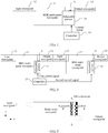
- FIG. 1 is a schematic structural diagram of an embodiment of a polarizer according to the present invention.
- a structure of the polarizer is schematically briefly illustrated by using FIG. 1 .
- the polarizer includes at least one multi-mode interference (Multi-Mode Interference, MMI for short) multi-mode waveguide.
- a waveguide refers to an apparatus that transmits an electromagnetic wave in a microwave band or a lightwave band and is used in radio fields such as the field of radio communications, the field of radars, and the field of navigation.
- the foregoing MMI waveguide is a wide waveguide device, in which an interference effect may occur in propagated optical signals in multiple lightwave modes, thereby outputting the optical signals at different end positions.
- FIG. 1 first shows a structure including only one MMI multi-mode waveguide.
- each MMI multi-mode waveguide 11 is connected to an input waveguide 12, and the input waveguide 12 is configured to input an optical signal in any polarization state; and the other side of the MMI multi-mode waveguide 11 is connected to an output waveguide 13, and the output waveguide 13 is configured to output an optical signal.
- an end portion of the side, on which the output waveguide 13 is located, of the MMI multi-mode waveguide 11 is provided with an adjustable portion 14.
- the adjustable portion 14 is in contact with and connected to the output waveguide 13, referring to a connection portion A.
- the MMI multi-mode waveguide 11, the input waveguide 12, the output waveguide 13, and the adjustable portion 14 are prepared on a semiconductor wafer (for example, silicon on an insulator) by using a standard complementary metal oxide semiconductor (Complementary Metal Oxide Semiconductor, CMOS for short) technology, and cling to each other on a same layer of planar waveguide.
- the polarizer further includes a controller 15 connected to the adjustable portion 14. Referring to an arrow shown in FIG.
- the controller 15 is connected to the adjustable portion 14 by means of a metal conducting wire or a metal pin on a chip.
- the controller 15 may apply a control signal to the adjustable portion 14 (in this embodiment of the present invention, a manner of connection between the controller 15 and the adjustable portion 14 is not limited as long as the control signal can be applied), to perform control to change a material property of the adjustable portion 14, so that the output waveguide 13 outputs optical signals in different polarization states.
- the foregoing material property of the adjustable portion 14 may be, for example, a refractive index or an absorption rate of the adjustable portion, that is, a change in the refractive index or the absorption rate can change a polarization state of an output optical signal.
- other properties such as a magnetic conductivity and a light transmittance
- a common material of the adjustable portion includes an alloy of silicon, a III- V compound, a high optical nonlinear compound, and the like.
- An optional example is as follows: When the controller applies no control signal, the output waveguide 13 outputs an optical signal in a TE polarization state; and when the controller applies a control signal to the adjustable portion 14, a refractive index of the adjustable portion 14 is changed, so that the output waveguide 13 outputs an optical signal in a TM polarization state. In this way, adjustability of polarization of the polarizer is implemented.
- the polarizer may include at least one MMI multi-mode waveguide, for example, the polarizer may include two, three, four, or even more MMI multi-mode waveguides.
- the polarizer may include two, three, four, or even more MMI multi-mode waveguides.
- an adjustable portion in each of the MMI multi-mode waveguides is connected to the controller.
- FIG. 2 is a schematic structural diagram of another embodiment of a polarizer according to the present invention.
- FIG. 2 shows an optional structure including two MMI multi-mode waveguides.
- the polarizer may include two sub-polarizers.
- Each sub-polarizer includes one MMI multi-mode waveguide, one input waveguide, and one output waveguide, and a structure of each sub-polarizer is the same as the structure shown in FIG. 1 .
- the two sub-polarizers are cascaded, that is, referring to FIG. 2 , an input waveguide of a sub-polarizer on the right side is connected to an output waveguide of a sub-polarizer on the left side.
- an optical signal that is output from the sub-polarizer on the left side may be used as an optical signal that is input to the sub-polarizer on the right side.
- the polarizer is disposed to have such a structure in which multiple sub-polarizers are cascaded, so that the polarizer can have a better polarization extinction ratio effect.
- the sub-polarizers in which the two MMI multi-mode waveguides are separately located may share a controller.
- the controller may apply a first control signal to one sub-polarizer, and apply a second control signal to the other sub-polarizer.
- the first control signal and the second control signal are the same.
- the controller may apply a first control signal to one sub-polarizer, so that the sub-polarizer outputs an optical signal in a TE polarization state; and the controller applies a second control signal that is the same as the first control signal to the other sub-polarizer, so that the sub-polarizer outputs an optical signal that is in a TE polarization state and has a better polarization extinction ratio.
- a manner of connection between multiple sub-polarizers may be a well-known connection manner, which is not described in detail in this embodiment.
- an output waveguide outputs optical signals in different polarization states, thereby implementing that a same polarizer can output optical signals in different polarization states, for example, the polarizer not only can output an optical signal in a TE polarization state, but also can output the optical signal in a TM polarization state.
- adjustable polarization is implemented.
- only one MMI multi-mode waveguide needs to be disposed between an input waveguide and an output waveguide; and the structure is simple and the costs are low.
- the adjustable portion in the polarizer there are various setting materials or setting manners.
- FIG. 3 is a schematic structural diagram of still another embodiment of a polarizer according to the present invention
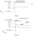
- FIG. 4 is a sectional view along an A-A direction in FIG. 3
- FIG. 5 is a sectional view along a B-B direction in FIG. 3
- An adjustable portion in this embodiment is provided with an electrode, and a controller may change an absorption rate of the adjustable portion by applying an electric field to the electrode.
- the adjustable portion is disposed to have a structure of a semiconductor p-i-n junction.
- the controller may be a programmable current source, such as an NI PXI programmable power module, or an iC-NZP series chip.
- each of an input waveguide, an output waveguide, and a multi-mode waveguide is a 3 -micron-thick silicon layer (that is, crystalline silicon c-Si), and there are a 2-micron-thick SiO 2 layer and a several-millimeter-thick silicon substrate below the silicon layer.
- the input waveguide and the output waveguide each include a straight waveguide that is 50 microns long, 3 microns high, and 1 micron wide and a tapered waveguide that is 50 microns long, 3 microns high, and 1 micron to 1.5 microns wide in linear growth.
- the multi-mode waveguide is 602 microns long, 3 microns high, and 8 microns wide.
- the adjustable portion in this embodiment is a rectangular SiGe alloy having a length range of 25 microns to 35 microns and a width range of 5 microns to 7 microns.
- the SiGe alloy is 29 microns long and 6.5 microns wide.
- the SiGe alloy is used as an example herein, and in specific implementation, another semiconductor material having an electro-absorption effect may also be used.
- the length of 25 to 35 microns and the width of 5 to 7 microns may also be changed, for example, the length is 19 to 30 microns and the width is 4.5 to 7 microns, but in the case of the foregoing length of 29 microns and width of 6.5 microns, the polarizer can achieve a better extinction ratio effect.
- the electrode is at a top layer of the p-i-n junction.
- the adjustable portion sequentially includes an Al/Cu electrode, an n+ Si layer, a SiGe alloy, and a p+ Si layer from top to bottom, thereby forming the p-i-n junction.
- An absorption rate of the foregoing semiconductor material SiGe alloy may change as an external electric field changes.
- an absorption coefficient, that is, the absorption rate, of the SiGe alloy for input light changes as the external electric field changes, thereby changing propagation paths of optical signals in different polarization states in the multi-mode waveguide and implementing a function of selection on a polarization state of an output optical signal.
- FIG. 6 is a schematic diagram 1 of emulation results of light fields in still another embodiment of a polarizer according to the present invention.
- FIG. 6 shows emulation results of light fields, which are in a 3D-BPM, of an MMI type polarizer that 1550 nm optical signals in TE and TM polarization states pass through when the controller applies no external electric field.
- a TE mode is reflected before an output port of the output waveguide, and therefore the TE mode misses the output waveguide and is leaked into a coverage layer; and a self-imaging point of a TM mode is exactly located at the output port of the output waveguide, and therefore the TM mode is output from the output waveguide.
- the polarizer is used as a TM mode polarizer and has a polarization extinction ratio of 12 dB.
- FIG. 7 is a schematic diagram 2 of emulation results of light fields in still another embodiment of a polarizer according to the present invention.
- FIG. 7 shows emulation results of light fields, in a 3D-BPM, of an MMI type polarizer that 1550 nm optical signals in TE and TM polarization states pass through when the controller applies an external electric field. It may be seen from FIG. 7 that, because of a property of strong absorption of the SiGe alloy under the external electric field, some of energy of light of a reflected TE mode is absorbed, and remaining energy is output from an output port; and during transmission, a TM mode is almost absorbed completely by the SiGe alloy and therefore cannot be output from the output waveguide.
- the polarizer is used as a TE mode polarizer and has a polarization extinction ratio of 7 dB.
- FIG. 8 is a schematic diagram of a polarization extinction ratio in still another embodiment of a polarizer according to the present invention and shows polarization extinction ratios in two states in which an external electric field is applied to a communication band and no external electric field is applied to a communication band. It may be seen from FIG. 8 that, a polarization extinction ratio of a TM mode is around 11 dB, and a polarization extinction ratio of a TE mode is around 7 dB.
- FIG. 9 is a schematic structural diagram of still another embodiment of a polarizer according to the present invention
- FIG. 10 is a sectional view along a C-C direction in FIG. 9
- FIG. 11 is a sectional view along a D-D direction in FIG. 9
- the polarizer in this embodiment differs from the polarizer in Embodiment 1 in that, in an adjustable portion of an MMI multi-mode waveguide, the semiconductor material having a changeable absorption rate in Embodiment 1 is replaced with a material whose refractive index is changeable under an external electric field, so that the adjustable portion becomes an area whose refractive index may be changed by a controller by applying an electric field to an electrode.
- each of an input waveguide and an output waveguide in this embodiment may be a straight waveguide, a curved waveguide, a stripe waveguide, a ridge waveguide, a tapered waveguide, a slotted waveguide, or the like.
- An input waveguide and output waveguide shown in FIG. 9 are of a structure of a straight waveguide.
- the adjustable portion of the polarizer in this embodiment may also be designed to have a structure of a p-i-n junction, and certainly, may also be designed to have another structure rather than the p-i-n junction.
- the input waveguide, the output waveguide, and the multi-mode waveguide are crystalline silicon (c-Si), and below a silicon layer, there are still a SiO 2 layer and a several-millimeter-thick silicon substrate.
- the electrode is at a top layer. Below the electrode, there is a semiconductor material whose refractive index may change as an external electric field changes, such as Si or a III- V compound.
- the controller may change a refractive index of the area by applying a changing external electric field.
- the refractive index changeable area below the electrode may include an n+ Si layer, a semiconductor material (a material whose refractive index is changeable under an external electric field), and a p+ Si layer.
- the refractive index of the semiconductor material in the refractive index changeable area may change as an external electric field changes.
- a refractive coefficient, that is, the refractive index, of the semiconductor material for input light changes as the external electric field changes, thereby changing propagation paths of optical signals in different polarization states in the multi-mode waveguide and implementing a function of selection on a polarization state of an output optical signal.
- the MMI multi-mode waveguide, the input waveguide, and the output waveguide in this embodiment may be made by using a material such as a semiconductor, a polymer, SiO 2 , or nitride.
- a size of the adjustable portion, such as a length and a width of the semiconductor material may be specifically set according to a used material, which is not limited in this embodiment of the present invention.
- an adjustable portion in an MMI multi-mode waveguide may include a thermo-optical material (such as a polymer) or a magneto-optical material (such as an yttrium iron garnet).
- a controller may change a refractive index of the thermo-optical material or the magneto-optical material, an absorption rate of the thermo-optical material or the magneto-optical material, a magnetic conductivity of the thermo-optical material or magneto-optical material, or a light transmittance of the thermo-optical material or the magneto-optical material by applying a temperature field to the thermo-optical material or by applying a magnetic field to the magneto-optical material.
- FIG. 12 is a schematic structural diagram of still another embodiment of a polarizer according to the present invention
- FIG. 13 is a sectional view along an E-E direction in FIG. 12
- FIG. 14 is a sectional view along an F-F direction in FIG. 12 .
- the polarizer in this embodiment differs from the polarizer in Embodiment 2 in that, in the adjustable portion of the MMI multi-mode waveguide, the semiconductor material whose refractive index is changeable under electricity in Embodiment 2 is replaced with a thermo-optical material whose refractive index is changeable under an external thermal field, and the common electrode in Embodiment 2 is replaced with a thermode, so that the adjustable portion becomes an area whose refractive index may be changed by a controller by controlling a temperature of the thermode.
- thermode in this embodiment may also be replaced with a pair of magnetic poles
- thermo-optical material in this embodiment may also be replaced with a magneto-optical material, so that the adjustable portion becomes an area whose refractive index may be changed by the controller by controlling a magnetic field of the magnetic poles.
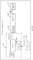
- FIG. 15 is a schematic structural diagram of an embodiment of a polarization modulation system according to the present invention.
- the system may include a polarizer 1501, a polarization beam splitter 1502, a differentiator 1503, a photoelectric detector 1504, and an encoder 1505 that are sequentially connected, where the polarizer 1501 may be the polarizer according to any embodiment of the present invention.
- the differentiator 1503, the photoelectric detector 1504, and the encoder 1505 in this embodiment reference may be made to various existing devices, which are not described in detail in this embodiment.
- the encoder 1505, the polarizer 1501, the polarization beam splitter 1502, the differentiator 1503, and the photoelectric detector 1504 are sequentially connected, and the connection manner thereof is not limited herein.
- FIG. 15 For a flow direction of a signal of the polarization modulation system, reference may be made to FIG. 15 .
- the encoder 1505 applies a preset coded signal to a controller, and the controller applies a control signal, so that an output port of the polarizer outputs two channels of complementary signals that are in different polarization states (actually, a whole including the polarizer and the controller in FIG. 15 is a polarizer; in this embodiment, components in FIG. 15 are shown in a manner for ease of description, and a block that indicates the polarizer in FIG.
- the signal actually includes an MMI multi-mode waveguide, an input waveguide, and an output waveguide), that is, a TE mode is 101010... and a TM mode is 010101.... Then, the signals enter two channels after passing through the polarization beam splitter 1502, and a differential signal with a light intensity of 202020... is produced in the differentiator 1503 and last is detected by the photoelectric detector 1504.
- a same channel of data is transmitted by means of two channels of optical signals that are in different polarization states, and last, a signal-to-noise ratio of an entire transmission system is improved by using a differentiator. Therefore, within a tolerance range of a PMD, an optical signal noise ratio (Optical Signal Noise Ratio, OSNR for short) of 3 dB can be improved.
- OSNR Optical Signal Noise Ratio
- the program may be stored in a computer-readable storage medium.
- the foregoing storage medium includes: any medium that can store program code, such as a ROM, a RAM, a magnetic disk, or an optical disc.
Landscapes
- Physics & Mathematics (AREA)
- Nonlinear Science (AREA)
- General Physics & Mathematics (AREA)
- Optics & Photonics (AREA)
- Engineering & Computer Science (AREA)
- Power Engineering (AREA)
- Microelectronics & Electronic Packaging (AREA)
- Optical Modulation, Optical Deflection, Nonlinear Optics, Optical Demodulation, Optical Logic Elements (AREA)
- Optical Integrated Circuits (AREA)
Claims (12)
- Polarisator, umfassend mindestens einen MMI-Mehrmodenwellenleiter (11), wobei jeweils eine Seite jedes MMI-Mehrmodenwellenleiters mit einem Eingangswellenleiter (12) und die jeweils andere Seite mit einem Ausgangswellenleiter (13) verbunden ist,
ein Endstück des MMI-Mehrmodenwellenleiters auf der Seite, an der sich der Ausgangswellenleiter befindet, mit einem justierbaren Teilstück (14) versehen und das justierbare Teilstück (14) mit dem Ausgangswellenleiter (13) verbunden ist, und der Polarisator ferner eine mit dem justierbaren Teilstück verbundene Steuereinheit (15) umfasst, wobei die Steuereinheit dazu ausgebildet ist, die Steuerung zum Ändern einer Materialeigenschaft des justierbaren Teilstücks auszuführen, so dass der Ausgangswellenleiter ein optisches Signal in einem TE-Polarisationszustand oder ein optisches Signal in einem TM-Polarisationszustand ausgibt. - Polarisator nach Anspruch 1, wobei der Ausgangswellenleiter ein optisches Signal in einem TE-Polarisationszustand ausgibt, wenn die Steuereinheit kein Steuersignal anlegt, und der Ausgangswellenleiter ein optisches Signal in einem TM-Polarisationszustand ausgibt, wenn die Steuereinheit ein Steuersignal an das justierbare Teilstück anlegt.
- Polarisator nach Anspruch 1 oder 2, wobei die Materialeigenschaft des justierbaren Teilstücks einen Brechungsindex des justierbaren Teilstücks und/oder eine magnetische Leitfähigkeit des justierbaren Teilstücks und/oder einen Lichttransmissionsgrad des justierbaren Teilstücks umfasst.
- Polarisator nach Anspruch 1 oder 2, wobei die Materialeigenschaft des justierbaren Teilstücks eine Absorptionsrate des justierbaren Teilstücks umfasst.
- Polarisator nach Anspruch 3, wobei
das justierbare Teilstück eine Elektrode und einen pin-Übergang umfasst und
die Steuereinheit dazu ausgebildet ist, einen Brechungsindex, eine magnetische Leitfähigkeit und/oder einen Lichttransmissionsgrad eines Bereiches des pin-Übergangs des justierbaren Teilstücks durch das Anlegen eines elektrischen Feldes an die Elektrode zu ändern. - Polarisator nach Anspruch 4, wobei
das justierbare Teilstück eine Elektrode und einen pin-Übergang umfasst und
die Steuereinheit dazu ausgebildet ist, eine Absorptionsrate eines Bereiches des pin-Übergangs des justierbaren Teilstücks durch das Anlegen eines elektrischen Feldes an die Elektrode zu ändern. - Polarisator nach Anspruch 5 oder 6, wobei der pin-Übergang eine SiGe-Legierung umfasst und die SiGe-Legierung einen Längenbereich von 25 bis 35 µm und einen Breitenbereich von 5 bis 7 µm aufweist.
- Polarisator nach Anspruch 7, wobei die SiGe-Legierung 29 µm lang und 6,5 µm breit ist.
- Polarisator nach Anspruch 3, wobei das justierbare Teilstück ein thermooptisches Material umfasst und
die Steuereinheit dazu ausgebildet ist, einen Brechungsindex, eine magnetische Leitfähigkeit und/oder einen Lichttransmissionsgrad des thermooptischen Materials durch Anlegen eines Temperaturfeldes an das thermooptische Material zu ändern,
oder
wobei das justierbare Teilstück ein magnetooptisches Material umfasst und
die Steuereinheit dazu ausgebildet ist, einen Brechungsindex, eine magnetische Leitfähigkeit und/oder einen Lichttransmissionsgrad des magnetooptischen Materials durch Anlegen eines Magnetfeldes an das magnetooptische Material zu ändern. - Polarisator nach Anspruch 4, wobei
das justierbare Teilstück ein thermooptisches Material umfasst und
die Steuereinheit dazu ausgebildet ist, eine Absorptionsrate des thermooptischen Materials durch Anlegen eines Temperaturfeldes an das thermooptische Material zu ändern,
oder
wobei das justierbare Teilstück ein magnetooptisches Material umfasst und
die Steuereinheit dazu ausgebildet ist, eine Absorptionsrate des magnetooptischen Materials durch Anlegen eines Magnetfeldes an das magnetooptische Material zu ändern. - Polarisator nach einem der Ansprüche 1 bis 10, wobei,
wenn der Polarisator mindestens zwei MMI-Multimodenwellenleiter umfasst, der Polarisator mindestens zwei Sub-Polarisatoren umfasst, wobei jeder der Sub-Polarisatoren einen MMI-Multimodenwellenleiter, einen Eingangswellenleiter und einen Ausgangswellenleiter umfasst und die mindestens zwei Sub-Polarisatoren eine Kaskade bilden. - Polarisationsmodulationssystem, umfassend den Polarisator nach einem der Ansprüche 1 bis 11 sowie ferner umfassend einen Encoder, einen Polarisations-Strahlenteiler, einen Differentiator und einen fotoelektrischen Detektor, wobei der Encoder, der Polarisator, der Polarisations-Strahlenteiler und der fotoelektrische Detektor aufeinanderfolgend verbunden sind.
Applications Claiming Priority (1)
| Application Number | Priority Date | Filing Date | Title |
|---|---|---|---|
| PCT/CN2013/090151 WO2015089844A1 (zh) | 2013-12-20 | 2013-12-20 | 起偏器及偏振调制系统 |
Publications (3)
| Publication Number | Publication Date |
|---|---|
| EP3073302A1 EP3073302A1 (de) | 2016-09-28 |
| EP3073302A4 EP3073302A4 (de) | 2016-11-09 |
| EP3073302B1 true EP3073302B1 (de) | 2018-09-26 |
Family
ID=53402009
Family Applications (1)
| Application Number | Title | Priority Date | Filing Date |
|---|---|---|---|
| EP13899938.8A Active EP3073302B1 (de) | 2013-12-20 | 2013-12-20 | Polarisator und polarisationsmodulationssystem |
Country Status (5)
| Country | Link |
|---|---|
| US (1) | US10067363B2 (de) |
| EP (1) | EP3073302B1 (de) |
| JP (1) | JP6226496B2 (de) |
| CN (1) | CN105829935A (de) |
| WO (1) | WO2015089844A1 (de) |
Families Citing this family (5)
| Publication number | Priority date | Publication date | Assignee | Title |
|---|---|---|---|---|
| US9746609B2 (en) * | 2015-06-30 | 2017-08-29 | Elenion Technologies, Llc | Integrated on-chip polarizer |
| US10731988B1 (en) * | 2019-07-10 | 2020-08-04 | Anello Photonics, Inc. | System architecture for integrated photonics optical gyroscopes |
| CN111458795B (zh) * | 2020-05-18 | 2024-04-30 | 浙江大学 | 一种基于硅波导的全波段起偏器 |
| CN115903277A (zh) * | 2021-09-30 | 2023-04-04 | 武汉光迅科技股份有限公司 | 一种光衰减器 |
| US20250189860A1 (en) * | 2023-12-08 | 2025-06-12 | Lumentum Technology (UK) Limited | Integrated variable optical attenuator |
Family Cites Families (17)
| Publication number | Priority date | Publication date | Assignee | Title |
|---|---|---|---|---|
| US5630004A (en) * | 1994-09-09 | 1997-05-13 | Deacon Research | Controllable beam director using poled structure |
| AUPP930799A0 (en) * | 1999-03-18 | 1999-04-15 | University Of Sydney, The | Optical planar waveguide device and method of its fabrication |
| JP2001183710A (ja) * | 1999-12-27 | 2001-07-06 | Kddi Corp | 多モード干渉導波路型光スイッチ |
| JP2002026820A (ja) * | 2000-07-12 | 2002-01-25 | Nippon Telegr & Teleph Corp <Ntt> | 光通信方法および光通信システム |
| WO2002103402A2 (en) * | 2001-06-18 | 2002-12-27 | Orchid Lightwave Communications, Inc. | Electro-optic waveguide modulator method and apparatus |
| GB0124840D0 (en) * | 2001-10-16 | 2001-12-05 | Univ Nanyang | A polarization beam splitter |
| GB0126621D0 (en) * | 2001-11-06 | 2002-01-02 | Univ Nanyang | A multimode interference (MMI) device |
| JP2003329986A (ja) * | 2002-05-15 | 2003-11-19 | Fujitsu Ltd | 光変調器および光導波路デバイス |
| JP2005221999A (ja) * | 2004-02-09 | 2005-08-18 | Fuji Xerox Co Ltd | 光変調器及び光変調器アレイ |
| US20050201715A1 (en) * | 2004-03-29 | 2005-09-15 | Panorama Flat Ltd. | System, method, and computer program product for magneto-optic device display |
| US7724987B2 (en) | 2004-12-13 | 2010-05-25 | Fujitsu Limited | Method and apparatus for dynamic polarization control |
| CN100538413C (zh) * | 2007-03-13 | 2009-09-09 | 浙江大学 | 基于光子晶体和多模干涉耦合器混合型的偏振分束器 |
| JP2009300888A (ja) * | 2008-06-16 | 2009-12-24 | Fujitsu Ltd | 光導波路デバイス |
| US9091813B2 (en) * | 2011-06-08 | 2015-07-28 | Skorpios Technologies, Inc. | Systems and methods for photonic polarization beam splitters |
| CN102841407B (zh) * | 2012-09-20 | 2014-06-04 | 电子科技大学 | 一种波导型偏振光分束器 |
| CN103148787B (zh) * | 2013-03-05 | 2016-12-07 | 北京航空航天大学 | 一种古斯汉欣位移传感测量方法及系统 |
| CN103424893B (zh) * | 2013-08-23 | 2015-11-11 | 西安电子科技大学 | 光学偏振变换器及其制作方法 |
-
2013
- 2013-12-20 JP JP2016541480A patent/JP6226496B2/ja active Active
- 2013-12-20 WO PCT/CN2013/090151 patent/WO2015089844A1/zh not_active Ceased
- 2013-12-20 EP EP13899938.8A patent/EP3073302B1/de active Active
- 2013-12-20 CN CN201380081689.9A patent/CN105829935A/zh active Pending
-
2016
- 2016-06-20 US US15/187,328 patent/US10067363B2/en active Active
Non-Patent Citations (1)
| Title |
|---|
| None * |
Also Published As
| Publication number | Publication date |
|---|---|
| WO2015089844A1 (zh) | 2015-06-25 |
| JP6226496B2 (ja) | 2017-11-08 |
| CN105829935A (zh) | 2016-08-03 |
| EP3073302A1 (de) | 2016-09-28 |
| JP2017504062A (ja) | 2017-02-02 |
| US10067363B2 (en) | 2018-09-04 |
| US20170023808A1 (en) | 2017-01-26 |
| EP3073302A4 (de) | 2016-11-09 |
Similar Documents
| Publication | Publication Date | Title |
|---|---|---|
| JP6198091B2 (ja) | 導波路偏光スプリッタ兼偏光回転子 | |
| US8649639B2 (en) | Method and system for waveguide mode filters | |
| US9122006B1 (en) | Integrated polarization splitter and rotator | |
| US8340478B2 (en) | Resonant optical modulators | |
| EP3938822B1 (de) | Polarisationsunabhängige photonische vorrichtung mit multimode-komponente | |
| Akiyama et al. | Compact PIN-diode-based silicon modulator using side-wall-grating waveguide | |
| Zhao et al. | Metawaveguide for asymmetric interferometric light-light switching | |
| US10067363B2 (en) | Polarizer and polarization modulation system | |
| CN103091869B (zh) | 集成化的相干光通信用电光调制器结构 | |
| Yamashita et al. | Design and fabrication of broadband PLC-based two-mode multi/demultiplexer using a wavefront matching method | |
| Fujisawa et al. | Low-Loss Cascaded Mach–Zehnder Multiplexer Integrated $25\hbox {-}{\rm Gbit}/{\rm s}\times 4\hbox {-}{\rm Lane} $ EADFB Laser Array for Future CFP4 100 GbE Transmitter | |
| US10422957B2 (en) | Method and system for a low-loss optical Y-junction power splitter | |
| EP3001241B1 (de) | Optoisolator | |
| CN104280823A (zh) | 一种基于波导结构的新型光隔离器 | |
| Chen et al. | Analysis of a silicon reconfigurable feed-forward optical delay line | |
| KR101550502B1 (ko) | 편광 모드 제어 기능을 이용한 평면 도파로 집적형 광 아이솔레이터 및 서큘레이터 | |
| EP2871504A1 (de) | Optische Moduslenkung zur Wellenlängenstabilisierung | |
| US10852570B1 (en) | Dual-slab-layer low-loss silicon optical modulator | |
| Biberman et al. | Thermally active 4× 4 non-blocking switch for networks-on-chip | |
| EP3312647B1 (de) | Polarisationsmodenwandler | |
| Mortazy et al. | Mode coupling between substrate integrated waveguide and coplanar waveguide for traveling-wave electrooptical modulator | |
| CN108710175B (zh) | 一种基于多模干涉耦合器的光开关、制作方法和光电子器件 | |
| Hu et al. | A novel MZ modulator based on photonic crystal and nanowire waveguide | |
| Huang et al. | Systematic investigation of silicon digital 1× 2 electro-optic switch based on a microdisk resonator through carrier injection | |
| Sawada et al. | CMOS-compatible Si-wire polarization beam splitter based on wavelength-insensitive coupler |
Legal Events
| Date | Code | Title | Description |
|---|---|---|---|
| PUAI | Public reference made under article 153(3) epc to a published international application that has entered the european phase |
Free format text: ORIGINAL CODE: 0009012 |
|
| 17P | Request for examination filed |
Effective date: 20160621 |
|
| AK | Designated contracting states |
Kind code of ref document: A1 Designated state(s): AL AT BE BG CH CY CZ DE DK EE ES FI FR GB GR HR HU IE IS IT LI LT LU LV MC MK MT NL NO PL PT RO RS SE SI SK SM TR |
|
| AX | Request for extension of the european patent |
Extension state: BA ME |
|
| A4 | Supplementary search report drawn up and despatched |
Effective date: 20161012 |
|
| RIC1 | Information provided on ipc code assigned before grant |
Ipc: G02B 6/27 20060101AFI20161006BHEP |
|
| DAX | Request for extension of the european patent (deleted) | ||
| 17Q | First examination report despatched |
Effective date: 20170822 |
|
| GRAP | Despatch of communication of intention to grant a patent |
Free format text: ORIGINAL CODE: EPIDOSNIGR1 |
|
| INTG | Intention to grant announced |
Effective date: 20180423 |
|
| GRAS | Grant fee paid |
Free format text: ORIGINAL CODE: EPIDOSNIGR3 |
|
| GRAA | (expected) grant |
Free format text: ORIGINAL CODE: 0009210 |
|
| AK | Designated contracting states |
Kind code of ref document: B1 Designated state(s): AL AT BE BG CH CY CZ DE DK EE ES FI FR GB GR HR HU IE IS IT LI LT LU LV MC MK MT NL NO PL PT RO RS SE SI SK SM TR |
|
| REG | Reference to a national code |
Ref country code: GB Ref legal event code: FG4D |
|
| REG | Reference to a national code |
Ref country code: CH Ref legal event code: EP |
|
| REG | Reference to a national code |
Ref country code: AT Ref legal event code: REF Ref document number: 1046699 Country of ref document: AT Kind code of ref document: T Effective date: 20181015 |
|
| REG | Reference to a national code |
Ref country code: IE Ref legal event code: FG4D |
|
| REG | Reference to a national code |
Ref country code: DE Ref legal event code: R096 Ref document number: 602013044338 Country of ref document: DE |
|
| REG | Reference to a national code |
Ref country code: NL Ref legal event code: MP Effective date: 20180926 |
|
| PG25 | Lapsed in a contracting state [announced via postgrant information from national office to epo] |
Ref country code: FI Free format text: LAPSE BECAUSE OF FAILURE TO SUBMIT A TRANSLATION OF THE DESCRIPTION OR TO PAY THE FEE WITHIN THE PRESCRIBED TIME-LIMIT Effective date: 20180926 Ref country code: RS Free format text: LAPSE BECAUSE OF FAILURE TO SUBMIT A TRANSLATION OF THE DESCRIPTION OR TO PAY THE FEE WITHIN THE PRESCRIBED TIME-LIMIT Effective date: 20180926 Ref country code: GR Free format text: LAPSE BECAUSE OF FAILURE TO SUBMIT A TRANSLATION OF THE DESCRIPTION OR TO PAY THE FEE WITHIN THE PRESCRIBED TIME-LIMIT Effective date: 20181227 Ref country code: NO Free format text: LAPSE BECAUSE OF FAILURE TO SUBMIT A TRANSLATION OF THE DESCRIPTION OR TO PAY THE FEE WITHIN THE PRESCRIBED TIME-LIMIT Effective date: 20181226 Ref country code: BG Free format text: LAPSE BECAUSE OF FAILURE TO SUBMIT A TRANSLATION OF THE DESCRIPTION OR TO PAY THE FEE WITHIN THE PRESCRIBED TIME-LIMIT Effective date: 20181226 Ref country code: SE Free format text: LAPSE BECAUSE OF FAILURE TO SUBMIT A TRANSLATION OF THE DESCRIPTION OR TO PAY THE FEE WITHIN THE PRESCRIBED TIME-LIMIT Effective date: 20180926 Ref country code: LT Free format text: LAPSE BECAUSE OF FAILURE TO SUBMIT A TRANSLATION OF THE DESCRIPTION OR TO PAY THE FEE WITHIN THE PRESCRIBED TIME-LIMIT Effective date: 20180926 |
|
| REG | Reference to a national code |
Ref country code: LT Ref legal event code: MG4D |
|
| PG25 | Lapsed in a contracting state [announced via postgrant information from national office to epo] |
Ref country code: HR Free format text: LAPSE BECAUSE OF FAILURE TO SUBMIT A TRANSLATION OF THE DESCRIPTION OR TO PAY THE FEE WITHIN THE PRESCRIBED TIME-LIMIT Effective date: 20180926 Ref country code: AL Free format text: LAPSE BECAUSE OF FAILURE TO SUBMIT A TRANSLATION OF THE DESCRIPTION OR TO PAY THE FEE WITHIN THE PRESCRIBED TIME-LIMIT Effective date: 20180926 Ref country code: LV Free format text: LAPSE BECAUSE OF FAILURE TO SUBMIT A TRANSLATION OF THE DESCRIPTION OR TO PAY THE FEE WITHIN THE PRESCRIBED TIME-LIMIT Effective date: 20180926 |
|
| REG | Reference to a national code |
Ref country code: AT Ref legal event code: MK05 Ref document number: 1046699 Country of ref document: AT Kind code of ref document: T Effective date: 20180926 |
|
| PG25 | Lapsed in a contracting state [announced via postgrant information from national office to epo] |
Ref country code: ES Free format text: LAPSE BECAUSE OF FAILURE TO SUBMIT A TRANSLATION OF THE DESCRIPTION OR TO PAY THE FEE WITHIN THE PRESCRIBED TIME-LIMIT Effective date: 20180926 Ref country code: NL Free format text: LAPSE BECAUSE OF FAILURE TO SUBMIT A TRANSLATION OF THE DESCRIPTION OR TO PAY THE FEE WITHIN THE PRESCRIBED TIME-LIMIT Effective date: 20180926 Ref country code: CZ Free format text: LAPSE BECAUSE OF FAILURE TO SUBMIT A TRANSLATION OF THE DESCRIPTION OR TO PAY THE FEE WITHIN THE PRESCRIBED TIME-LIMIT Effective date: 20180926 Ref country code: PL Free format text: LAPSE BECAUSE OF FAILURE TO SUBMIT A TRANSLATION OF THE DESCRIPTION OR TO PAY THE FEE WITHIN THE PRESCRIBED TIME-LIMIT Effective date: 20180926 Ref country code: IS Free format text: LAPSE BECAUSE OF FAILURE TO SUBMIT A TRANSLATION OF THE DESCRIPTION OR TO PAY THE FEE WITHIN THE PRESCRIBED TIME-LIMIT Effective date: 20190126 Ref country code: RO Free format text: LAPSE BECAUSE OF FAILURE TO SUBMIT A TRANSLATION OF THE DESCRIPTION OR TO PAY THE FEE WITHIN THE PRESCRIBED TIME-LIMIT Effective date: 20180926 Ref country code: AT Free format text: LAPSE BECAUSE OF FAILURE TO SUBMIT A TRANSLATION OF THE DESCRIPTION OR TO PAY THE FEE WITHIN THE PRESCRIBED TIME-LIMIT Effective date: 20180926 Ref country code: EE Free format text: LAPSE BECAUSE OF FAILURE TO SUBMIT A TRANSLATION OF THE DESCRIPTION OR TO PAY THE FEE WITHIN THE PRESCRIBED TIME-LIMIT Effective date: 20180926 Ref country code: IT Free format text: LAPSE BECAUSE OF FAILURE TO SUBMIT A TRANSLATION OF THE DESCRIPTION OR TO PAY THE FEE WITHIN THE PRESCRIBED TIME-LIMIT Effective date: 20180926 |
|
| PG25 | Lapsed in a contracting state [announced via postgrant information from national office to epo] |
Ref country code: SM Free format text: LAPSE BECAUSE OF FAILURE TO SUBMIT A TRANSLATION OF THE DESCRIPTION OR TO PAY THE FEE WITHIN THE PRESCRIBED TIME-LIMIT Effective date: 20180926 Ref country code: SK Free format text: LAPSE BECAUSE OF FAILURE TO SUBMIT A TRANSLATION OF THE DESCRIPTION OR TO PAY THE FEE WITHIN THE PRESCRIBED TIME-LIMIT Effective date: 20180926 Ref country code: PT Free format text: LAPSE BECAUSE OF FAILURE TO SUBMIT A TRANSLATION OF THE DESCRIPTION OR TO PAY THE FEE WITHIN THE PRESCRIBED TIME-LIMIT Effective date: 20190126 |
|
| REG | Reference to a national code |
Ref country code: DE Ref legal event code: R097 Ref document number: 602013044338 Country of ref document: DE |
|
| PG25 | Lapsed in a contracting state [announced via postgrant information from national office to epo] |
Ref country code: DK Free format text: LAPSE BECAUSE OF FAILURE TO SUBMIT A TRANSLATION OF THE DESCRIPTION OR TO PAY THE FEE WITHIN THE PRESCRIBED TIME-LIMIT Effective date: 20180926 |
|
| REG | Reference to a national code |
Ref country code: CH Ref legal event code: PL |
|
| PLBE | No opposition filed within time limit |
Free format text: ORIGINAL CODE: 0009261 |
|
| STAA | Information on the status of an ep patent application or granted ep patent |
Free format text: STATUS: NO OPPOSITION FILED WITHIN TIME LIMIT |
|
| GBPC | Gb: european patent ceased through non-payment of renewal fee |
Effective date: 20181226 |
|
| PG25 | Lapsed in a contracting state [announced via postgrant information from national office to epo] |
Ref country code: LU Free format text: LAPSE BECAUSE OF NON-PAYMENT OF DUE FEES Effective date: 20181220 Ref country code: MC Free format text: LAPSE BECAUSE OF FAILURE TO SUBMIT A TRANSLATION OF THE DESCRIPTION OR TO PAY THE FEE WITHIN THE PRESCRIBED TIME-LIMIT Effective date: 20180926 |
|
| 26N | No opposition filed |
Effective date: 20190627 |
|
| REG | Reference to a national code |
Ref country code: IE Ref legal event code: MM4A |
|
| REG | Reference to a national code |
Ref country code: BE Ref legal event code: MM Effective date: 20181231 |
|
| PG25 | Lapsed in a contracting state [announced via postgrant information from national office to epo] |
Ref country code: SI Free format text: LAPSE BECAUSE OF FAILURE TO SUBMIT A TRANSLATION OF THE DESCRIPTION OR TO PAY THE FEE WITHIN THE PRESCRIBED TIME-LIMIT Effective date: 20180926 Ref country code: FR Free format text: LAPSE BECAUSE OF NON-PAYMENT OF DUE FEES Effective date: 20181231 Ref country code: IE Free format text: LAPSE BECAUSE OF NON-PAYMENT OF DUE FEES Effective date: 20181220 |
|
| PG25 | Lapsed in a contracting state [announced via postgrant information from national office to epo] |
Ref country code: BE Free format text: LAPSE BECAUSE OF NON-PAYMENT OF DUE FEES Effective date: 20181231 |
|
| PG25 | Lapsed in a contracting state [announced via postgrant information from national office to epo] |
Ref country code: LI Free format text: LAPSE BECAUSE OF NON-PAYMENT OF DUE FEES Effective date: 20181231 Ref country code: CH Free format text: LAPSE BECAUSE OF NON-PAYMENT OF DUE FEES Effective date: 20181231 Ref country code: GB Free format text: LAPSE BECAUSE OF NON-PAYMENT OF DUE FEES Effective date: 20181226 |
|
| PG25 | Lapsed in a contracting state [announced via postgrant information from national office to epo] |
Ref country code: MT Free format text: LAPSE BECAUSE OF NON-PAYMENT OF DUE FEES Effective date: 20181220 |
|
| PG25 | Lapsed in a contracting state [announced via postgrant information from national office to epo] |
Ref country code: TR Free format text: LAPSE BECAUSE OF FAILURE TO SUBMIT A TRANSLATION OF THE DESCRIPTION OR TO PAY THE FEE WITHIN THE PRESCRIBED TIME-LIMIT Effective date: 20180926 |
|
| PG25 | Lapsed in a contracting state [announced via postgrant information from national office to epo] |
Ref country code: MK Free format text: LAPSE BECAUSE OF NON-PAYMENT OF DUE FEES Effective date: 20180926 Ref country code: CY Free format text: LAPSE BECAUSE OF FAILURE TO SUBMIT A TRANSLATION OF THE DESCRIPTION OR TO PAY THE FEE WITHIN THE PRESCRIBED TIME-LIMIT Effective date: 20180926 Ref country code: HU Free format text: LAPSE BECAUSE OF FAILURE TO SUBMIT A TRANSLATION OF THE DESCRIPTION OR TO PAY THE FEE WITHIN THE PRESCRIBED TIME-LIMIT; INVALID AB INITIO Effective date: 20131220 |
|
| P01 | Opt-out of the competence of the unified patent court (upc) registered |
Effective date: 20230524 |
|
| PGFP | Annual fee paid to national office [announced via postgrant information from national office to epo] |
Ref country code: DE Payment date: 20251104 Year of fee payment: 13 |