EP3070849A1 - Successive aproximation register analog to digital converters - Google Patents
Successive aproximation register analog to digital converters Download PDFInfo
- Publication number
- EP3070849A1 EP3070849A1 EP15170086.1A EP15170086A EP3070849A1 EP 3070849 A1 EP3070849 A1 EP 3070849A1 EP 15170086 A EP15170086 A EP 15170086A EP 3070849 A1 EP3070849 A1 EP 3070849A1
- Authority
- EP
- European Patent Office
- Prior art keywords
- output signal
- digital output
- voltage
- switch
- coupled
- Prior art date
- Legal status (The legal status is an assumption and is not a legal conclusion. Google has not performed a legal analysis and makes no representation as to the accuracy of the status listed.)
- Withdrawn
Links
- 239000003990 capacitor Substances 0.000 claims abstract description 95
- 238000006243 chemical reaction Methods 0.000 claims abstract description 29
- 238000000605 extraction Methods 0.000 claims abstract description 24
- 238000001914 filtration Methods 0.000 claims abstract description 8
- 230000000875 corresponding effect Effects 0.000 description 11
- 238000000034 method Methods 0.000 description 5
- 238000013459 approach Methods 0.000 description 3
- 230000002596 correlated effect Effects 0.000 description 2
- 238000012986 modification Methods 0.000 description 2
- 230000004048 modification Effects 0.000 description 2
- 238000004891 communication Methods 0.000 description 1
- 238000010276 construction Methods 0.000 description 1
- 239000000284 extract Substances 0.000 description 1
- 230000010354 integration Effects 0.000 description 1
- 238000005259 measurement Methods 0.000 description 1
- 230000000717 retained effect Effects 0.000 description 1
- 238000005070 sampling Methods 0.000 description 1
- 238000012360 testing method Methods 0.000 description 1
Images



Classifications
-
- H—ELECTRICITY
- H03—ELECTRONIC CIRCUITRY
- H03M—CODING; DECODING; CODE CONVERSION IN GENERAL
- H03M1/00—Analogue/digital conversion; Digital/analogue conversion
- H03M1/12—Analogue/digital converters
- H03M1/34—Analogue value compared with reference values
- H03M1/38—Analogue value compared with reference values sequentially only, e.g. successive approximation type
- H03M1/46—Analogue value compared with reference values sequentially only, e.g. successive approximation type with digital/analogue converter for supplying reference values to converter
- H03M1/466—Analogue value compared with reference values sequentially only, e.g. successive approximation type with digital/analogue converter for supplying reference values to converter using switched capacitors
- H03M1/468—Analogue value compared with reference values sequentially only, e.g. successive approximation type with digital/analogue converter for supplying reference values to converter using switched capacitors in which the input S/H circuit is merged with the feedback DAC array
-
- H—ELECTRICITY
- H03—ELECTRONIC CIRCUITRY
- H03M—CODING; DECODING; CODE CONVERSION IN GENERAL
- H03M1/00—Analogue/digital conversion; Digital/analogue conversion
- H03M1/06—Continuously compensating for, or preventing, undesired influence of physical parameters
- H03M1/0617—Continuously compensating for, or preventing, undesired influence of physical parameters characterised by the use of methods or means not specific to a particular type of detrimental influence
- H03M1/0634—Continuously compensating for, or preventing, undesired influence of physical parameters characterised by the use of methods or means not specific to a particular type of detrimental influence by averaging out the errors, e.g. using sliding scale
- H03M1/0636—Continuously compensating for, or preventing, undesired influence of physical parameters characterised by the use of methods or means not specific to a particular type of detrimental influence by averaging out the errors, e.g. using sliding scale in the amplitude domain
- H03M1/0639—Continuously compensating for, or preventing, undesired influence of physical parameters characterised by the use of methods or means not specific to a particular type of detrimental influence by averaging out the errors, e.g. using sliding scale in the amplitude domain using dither, e.g. using triangular or sawtooth waveforms
- H03M1/0641—Continuously compensating for, or preventing, undesired influence of physical parameters characterised by the use of methods or means not specific to a particular type of detrimental influence by averaging out the errors, e.g. using sliding scale in the amplitude domain using dither, e.g. using triangular or sawtooth waveforms the dither being a random signal
-
- H—ELECTRICITY
- H03—ELECTRONIC CIRCUITRY
- H03M—CODING; DECODING; CODE CONVERSION IN GENERAL
- H03M1/00—Analogue/digital conversion; Digital/analogue conversion
- H03M1/10—Calibration or testing
- H03M1/1004—Calibration or testing without interrupting normal operation, e.g. by providing an additional component for temporarily replacing components to be tested or calibrated
-
- H—ELECTRICITY
- H03—ELECTRONIC CIRCUITRY
- H03M—CODING; DECODING; CODE CONVERSION IN GENERAL
- H03M1/00—Analogue/digital conversion; Digital/analogue conversion
- H03M1/10—Calibration or testing
- H03M1/1009—Calibration
-
- H—ELECTRICITY
- H03—ELECTRONIC CIRCUITRY
- H03M—CODING; DECODING; CODE CONVERSION IN GENERAL
- H03M1/00—Analogue/digital conversion; Digital/analogue conversion
- H03M1/12—Analogue/digital converters
- H03M1/34—Analogue value compared with reference values
- H03M1/38—Analogue value compared with reference values sequentially only, e.g. successive approximation type
-
- H—ELECTRICITY
- H03—ELECTRONIC CIRCUITRY
- H03M—CODING; DECODING; CODE CONVERSION IN GENERAL
- H03M1/00—Analogue/digital conversion; Digital/analogue conversion
- H03M1/12—Analogue/digital converters
- H03M1/34—Analogue value compared with reference values
- H03M1/38—Analogue value compared with reference values sequentially only, e.g. successive approximation type
- H03M1/40—Analogue value compared with reference values sequentially only, e.g. successive approximation type recirculation type
-
- H—ELECTRICITY
- H03—ELECTRONIC CIRCUITRY
- H03M—CODING; DECODING; CODE CONVERSION IN GENERAL
- H03M1/00—Analogue/digital conversion; Digital/analogue conversion
- H03M1/12—Analogue/digital converters
- H03M1/34—Analogue value compared with reference values
- H03M1/38—Analogue value compared with reference values sequentially only, e.g. successive approximation type
- H03M1/40—Analogue value compared with reference values sequentially only, e.g. successive approximation type recirculation type
- H03M1/403—Analogue value compared with reference values sequentially only, e.g. successive approximation type recirculation type using switched capacitors
Definitions
- the invention relates to an analog to digital converter (ADC), and more particularly to an ADC that uses successive approximation techniques.
- ADC analog to digital converter
- ADCs Analog to digital converters
- SAR successive approximation register
- the conversion accuracy of the SAR ADCs is mainly subject to the DAC mismatch and offset errors. Particularly, for the switched-capacitor SAR ADCs, the capacitor mismatch is the dominant one..
- the SAR ADC circuit receives an analog input signal and operates in a sample phase and a conversion phase following the sample phase to generate a digital output signal.
- the SAR ADC circuit comprises a plurality of capacitors, a comparator, and a logic unit.
- the plurality of capacitors are coupled to a summing node.
- a target capacitor among the plurality of capacitors is coupled to a direct current (DC) voltage and the other capacitors among the plurality of capacitors are coupled to the analog input signal.
- the comparator has an input terminal coupled to the summing node.
- the comparator performs a comparison operation to a summing voltage at the summing node
- the logic unit has a plurality of weighting values corresponding to the plurality of capacitors respectively and generates the digital output signal according to the weighting values and a comparison result of the comparison operation.
- the DC voltage has a first voltage level or a second voltage level different from the first voltage level according to a random sequence.
- the weighting value of the target capacitor is calibrated according to the digital output signal and the random sequence.
- the SAR ADC circuit receives an analog input signal and operates in a sample phase and a conversion phase following the sample phase to generate a digital output signal.
- the SAR ADC circuit comprises a first switch, a plurality of capacitors, a plurality of second switches, a plurality of switch circuits, a comparator, a logic unit, and an extraction and compensation unit.
- the first switch is coupled between a first voltage and a summing node.
- Each capacitor has a first terminal coupled to the summing node and further has a second terminal.
- Each second switch is coupled between the second terminal of one of the plurality of capacitors and a second voltage.
- the plurality of switch circuits receives the analog input signal, Each switch circuits is coupled to the second terminal of one of the plurality of capacitors and, before the conversion phase, provides a DC voltage or the analog input signal to the corresponding capacitor.
- the comparator has an input terminal coupled to the summing node. In the conversion phase, the comparator performs a comparison operation to a summing voltage at the summing node.
- the logic unit has a plurality of weighting values corresponding to the plurality of capacitors respectively and generates the digital output signal according to the weighting values and a comparison result of the comparison operation.
- the extraction and compensation unit receives the digital output signal.
- the DC voltage When a target capacitor among the plurality of switch circuits receive the DC voltage from the corresponding switch circuit, the DC voltage has a first voltage level or a second voltage level different from the first voltage level based on a random sequence,.
- the extraction and compensation unit obtains a calibrated weighting value according to the digital output signal and the random sequence, and the calibrated weighting value serves as the weighting value of the target capacitor.
- FIG. 1 shows an exemplary embodiment of a successive approximation register (SAR) analog to digital converter (ADC) circuit.
- SAR successive approximation register
- ADC analog to digital converter
- an SAR ADC circuit 1 comprises an SAR DAC 10, and an extraction and compensation unit 11.
- the SAR ADC circuit 1 operates in a sample phase and a conversion phase following the sample phase in several cycles.
- the SAR ADC 10 receives an analog input signal V in and generates a digital output signal D o according to the analog input signal V in , weighting values of capacitors (shown in FIG.
- the digital output signal D o comprises one term related to the random signal q ⁇ V r .
- the extraction and compensation unit 11 extracts the real weighting value of the capacitor to be calibrated according to the digital output signal D o and the random signal q ⁇ V r . Then, the extraction and compensation unit 11 corrects the digital output signal D o based on the real weighting value of the capacitor to be calibrated
- the SAR DAC 10 comprises N capacitors C 0 ⁇ C N-1 , a sample switch SWS, N switches SW 0 ⁇ SW N-1 , N switch circuits SWC 0 ⁇ SWC N-1 , a comparator 20, and a logic unit 21, wherein N is an positive integer.
- the sample switch SWS is coupled to a summing node N20 and a signal.
- the signal which is coupled to the sample switch SWS is a ground voltage GND.
- One terminal of the comparator 20 is coupled to the summing node N20, and the other terminal thereof is coupled to the ground voltage GND.
- Each of the capacitors C 0 ⁇ C N-1 has two terminals. A first terminal of each capacitor is coupled to the summing node N20. In the embodiment, a second terminal of each capacitor is coupled to one switch SWj and one switch circuit SWC j , wherein 0 ⁇ j ⁇ N-1. For example, the other terminal of the capacitor C N-1 is coupled to the switch SW N-1 and the switch circuit SWC N-1 , and the other terminal of the capacitor Co is coupled to the switch SWo and the switch circuit SWC 0 .
- the sample switch SWS, the N switches SW 0 ⁇ SW N-1 , and the N switch circuits SWC 0 ⁇ SWC N-1 are controlled by the logic unit 21.
- the each of the switch circuits SWC 0 ⁇ SWC N-1 receives the analog input signal V in and the random signal q ⁇ Vr.
- Each switch circuit is controlled by the logic unit 21 to provide the analog input signal V in or a DC voltage to the corresponding capacitor.
- the level of the DC voltage is determined by the random signal q ⁇ Vr, that is the level of the DC voltage is the level of -V r or V r .
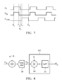
- FIG. 3 shows the timing of the sample phase and the conversion phase of the SAR ADC circuit 10
- ⁇ 1e represents the timing of the sample phase
- ⁇ SAR represents the timing of the conversion phase
- ⁇ 1 represents the timing of the operation of the switch circuits.
- the sample switch SWS is turned on.
- the corresponding switch circuit SWC j provides the DC voltage to the one capacitor C j
- the other switch circuits provide the analog input signal V in to the corresponding capacitors.
- the switches SW N-1 ⁇ SW 0 are sequentially turned on to provide the voltage Vr to the respective capacitors SW N-1 ⁇ SW 0 .
- the comparator 20 determines the binary code word from MSB b N-1 to the LSB bo by examining the polarity of the voltage at the summing node N20 sequentially.
- Q x , 1 c is equal to Q x, 2
- the weighting value of capacitor C j is desired to be calibrated.
- the R j V r ⁇ ( C j / C tot ) .represents the weighting value of capacitor C j and determines the real weighting value of the capacitor C j .
- the extraction and compensation unit 11 performs a correlation operation to the digital output signal D o with the random sequence q and further performs a low-pass-filtering operation to the digital output signal D o to generate a calibrated weighting value ⁇ j of the capacitor C j .
- the digital output signal Do is correlated with the random sequence q and then low-pass filtered to obtain the weighting value ⁇ j .
- the extraction and compensation unit 11 then corrects the digital output signal D o according to the calibrated weighting value ⁇ j to generate the output signal D C o
- FIG. 4 shows an exemplary embodiment of an extraction circuit 110 in the extraction and compensation unit 11.
- FIG. 4 also shows the SAR DAC 10.
- the extraction circuit 11 comprises a multiplier 40 and a low-pass filter (LPF) 41.
- the multiplier 40 receives the digital output signal D o and the random sequence q to achieve the correlation operation to the digital output signal D o and the random sequence q.
- the low-pass filter 41 is coupled to the multiplier 40 and performs the low-pass-filtering operation to the digital output signal D o to generate the calibrated weighting value ⁇ j .
- the term R j is retained, and the calibrated weighting value ⁇ j is the digital expression of the term R j .
- the calibrated weighting value ⁇ j related to the real weighting value of the capacitor C j is obtained and used to correct the digital output signal D o .
- the above operations performed to obtain the calibrated weighting value ⁇ j related to the real weighting value of the capacitor C j are also performed for the other capacitors required to be calibrated.
- the related description is omitted.
- the weighting values of the capacitors can be calibrated. Even though the capacitor mismatch occurs, the digital output signal Do can more approach the accurate digital value of the analog input signal V in .
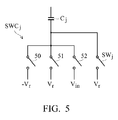
- FIG. 5 shows an exemplary embodiment of the switch circuits SWC 0 ⁇ SWC N-1 .
- the switch circuit SWC j comprises three switches 50-52.
- the switch 50 is coupled between the capacitor C j and the voltage Vr.
- the switch 51 is coupled between the capacitor C j and the voltage -Vr.
- the switch 52 is coupled between the capacitor C j and the analog input signal V in .
- the switches 50-52 are controlled by the logic unit 21 and not turned on at the same time.
- one of the three voltages Vr, -Vr, and V in serves as the DC voltage provided the capacitor C j .
- the logic unit 21 controls the switches 50 and 51 according to the random sequence q.
- the switch circuit SWC j receives the random signal q ⁇ Vr, which determines the voltage Vr or -Vr to be provided to the capacitor C j before the conversion phase.
- the DC voltage (Vr or -Vr) is provided to the capacitor C j to be calibrated in the period between the time point T1 and a time point T3, as shown by ⁇ 1 , however, without limitation.
- the DC voltage can be provided to the capacitor C j in any period which just occurs before the conversion phase occurs (that is before the time point T4).
- FIG. 6A shows another exemplary embodiment of the SAR ADC 10.
- the SAR ADC shown in FIG. 6A is a differential-type, 12-bit ADC.
- the signals which are coupled to the sample switches SWS are analog input signals V ip and V in .
- a switch group are coupled to the capacitors C 1 ⁇ C 11 .
- the switch group 60 comprises several switches and switch circuits as shown in FIG. 2 . Each set of one switch SW j and one switch circuit SWC j is coupled to the corresponding capacitor and performs the same operations of the embodiment of FIG. 2 .
- V rp replaces the V r to be provided to capacitors coupled to the positive input (+) of the comparator 20, while V rn replaces the V r to be provided to capacitors coupled to the negative input (-) of the comparator 20.
- the weighting values of the capacitors C 8 , C 9,0 ⁇ C 9,1 , C 10,0 ⁇ C 10,3 , and C 11,0 ⁇ C 11,7 are required to be calibrated.
- the calibration process of the capacitor C 8 is the similar to the above process for calibrating the weighting value of the capacitor C j .
- the digital output signal Do is correlated with the random q and then low-pass filtered.
- the low-pass filtering is achieved by integration and average operations. That is, the digital output signal Do is further integrated and divided by M cycles.
- the low-pass filter 41 is implemented by a digital accumulator (Digital Accumu.) 70 and a divider (1/M) 71.
- the calibrated weighting value of the capacitor C 8 is obtained as: W ⁇ 8 ⁇ C 8 C t o t ⁇ V r p - V r n
Landscapes
- Engineering & Computer Science (AREA)
- Theoretical Computer Science (AREA)
- Power Engineering (AREA)
- Analogue/Digital Conversion (AREA)
Abstract
a plurality of capacitors(C0, ..., CN-1) coupled to a summing node (N20), wherein before the conversion phase, a target capacitor (Cj) among the plurality of capacitors is coupled to a direct current voltage (q*VR) and the other capacitors among the plurality of capacitors are coupled to the analog input signal;
a comparator (20) having an input terminal coupled to the summing node, wherein in the conversion phase, the comparator performs a comparison operation to a summing voltage at the summing node; and
a logic unit (21) having a plurality of weighting values corresponding to the plurality of capacitors respectively and generating the digital output signal according to the weighting values and a comparison result of the comparison operation,
wherein the DC voltage has a first voltage level or a second voltage level different from the first voltage level according to a random sequence (q),
an extraction and compensation unit (11,110) receiving the digital output signal,
wherein the extraction and compensation unit performs a correlation operation (40) to the digital output signal with the random sequence and further performs a low-pass-filtering operation(41) to the digital output signal to generate a calibrated weighting value (Wj), and
wherein the extraction and compensation unit corrects the digital output signal based on the weighting value of the target capacitor and
wherein the weighting value of the target capacitor is calibrated according to the digital output signal and the random sequence.
Description
- The invention relates to an analog to digital converter (ADC), and more particularly to an ADC that uses successive approximation techniques.
- Analog to digital converters (ADCs) are widely used in a variety of applications, such as medical systems, audio systems, test and measurement equipment, communication systems, and image and video systems, etc. The most common ADC construction comprises flash ADCs, pipeline ADCs and successive approximation register (SAR) ADCs. The power consumption of the SAR ADC is smaller than the flash ADC and the pipeline ADC. Thus the systems with limited power supply, such as portable devices, usually use SAR ADCs.
- The conversion accuracy of the SAR ADCs is mainly subject to the DAC mismatch and offset errors. Particularly, for the switched-capacitor SAR ADCs, the capacitor mismatch is the dominant one..
- Thus, it is desired to provide a successive approximation register circuit which can correct error caused by the capacitor mismatch.
- An exemplary embodiment of a successive approximation register (SAR) analog to digital converter (ADC) circuit is provided. The SAR ADC circuit receives an analog input signal and operates in a sample phase and a conversion phase following the sample phase to generate a digital output signal. The SAR ADC circuit comprises a plurality of capacitors, a comparator, and a logic unit. The plurality of capacitors are coupled to a summing node. Before the conversion phase, a target capacitor among the plurality of capacitors is coupled to a direct current (DC) voltage and the other capacitors among the plurality of capacitors are coupled to the analog input signal. The comparator has an input terminal coupled to the summing node. In the conversion phase, the comparator performs a comparison operation to a summing voltage at the summing node The logic unit has a plurality of weighting values corresponding to the plurality of capacitors respectively and generates the digital output signal according to the weighting values and a comparison result of the comparison operation. The DC voltage has a first voltage level or a second voltage level different from the first voltage level according to a random sequence. The weighting value of the target capacitor is calibrated according to the digital output signal and the random sequence.
- An exemplary embodiment of a successive approximation register (SAR) analog to digital converter (ADC) circuit is provided. The SAR ADC circuit receives an analog input signal and operates in a sample phase and a conversion phase following the sample phase to generate a digital output signal. The SAR ADC circuit comprises a first switch, a plurality of capacitors, a plurality of second switches, a plurality of switch circuits, a comparator, a logic unit, and an extraction and compensation unit. The first switch is coupled between a first voltage and a summing node. Each capacitor has a first terminal coupled to the summing node and further has a second terminal. Each second switch is coupled between the second terminal of one of the plurality of capacitors and a second voltage. The plurality of switch circuits receives the analog input signal, Each switch circuits is coupled to the second terminal of one of the plurality of capacitors and, before the conversion phase, provides a DC voltage or the analog input signal to the corresponding capacitor. The comparator has an input terminal coupled to the summing node. In the conversion phase, the comparator performs a comparison operation to a summing voltage at the summing node. The logic unit has a plurality of weighting values corresponding to the plurality of capacitors respectively and generates the digital output signal according to the weighting values and a comparison result of the comparison operation. The extraction and compensation unit receives the digital output signal. When a target capacitor among the plurality of switch circuits receive the DC voltage from the corresponding switch circuit, the DC voltage has a first voltage level or a second voltage level different from the first voltage level based on a random sequence,. The extraction and compensation unit obtains a calibrated weighting value according to the digital output signal and the random sequence, and the calibrated weighting value serves as the weighting value of the target capacitor.
- A detailed description is given in the following embodiments with reference to the accompanying drawings.
- The invention can be more fully understood by reading the subsequent detailed description and examples with references made to the accompanying drawings, wherein:
-
FIG. 1 shows an exemplary embodiment of a successive approximation register (SAR) analog to digital converter (ADC) circuit; -
FIG. 2 shows an exemplary embodiment of an SAR DAC of the SAR ADC circuit inFIG. 1 ; -
FIG. 3 shows timing of a sample phase and a conversion phase of the SAR ADC circuit inFIG. 1 ; -
FIG. 4 shows an exemplary embodiment of an extraction and compensation unit of the SAR ADC circuit inFIG. 1 ; -
FIG. 5 shows an exemplary embodiment of switch circuits of the SAR ADC inFIG. 2 ; -
FIG. 6A and 6B show another exemplary embodiment of an SAR DAC of the SAR ADC circuit inFIG. 1 ; and -
FIG. 7 shows an exemplary embodiment of a low-pass filter. - The following description is of the best-contemplated mode of carrying out the invention. This description is made for the purpose of illustrating the general principles of the invention and should not be taken in a limiting sense. The scope of the invention is best determined by reference to the appended claims.
-
FIG. 1 shows an exemplary embodiment of a successive approximation register (SAR) analog to digital converter (ADC) circuit. As shown inFIG. 1 anSAR ADC circuit 1 comprises anSAR DAC 10, and an extraction andcompensation unit 11. The SARADC circuit 1 operates in a sample phase and a conversion phase following the sample phase in several cycles. TheSAR ADC 10 receives an analog input signal Vin and generates a digital output signal Do according to the analog input signal Vin, weighting values of capacitors (shown inFIG. 2 ), a direct current (DC) voltage, and a random signal q ·Vr-, wherein q represents is a binary value random sequence which is uncorrelated with the analog input signal Vin, and each value of the random sequence is equal to 1 or -1. Thus, the voltage level of the random signal q · Vr is the level of -Vr or Vr. In the embodiment, the random signal q · Vr is injected to at least one capacitor (shown inFIG. 2 ) to be calibrated in theSAR ADC 10. Thus, the digital output signal Do comprises one term related to the random signal q · Vr. The extraction andcompensation unit 11 extracts the real weighting value of the capacitor to be calibrated according to the digital output signal Do and the random signal q · Vr. Then, the extraction andcompensation unit 11 corrects the digital output signal Do based on the real weighting value of the capacitor to be calibrated - The detailed structure of the
SAR DAC 10 is shown inFIG. 2 . As shown inFIG. 2 , theSAR DAC 10 comprises N capacitors C0∼CN-1, a sample switch SWS, N switches SW0∼SWN-1, N switch circuits SWC0∼SWCN-1, acomparator 20, and alogic unit 21, wherein N is an positive integer. The sample switch SWS is coupled to a summing node N20 and a signal. In the embodiment, the signal which is coupled to the sample switch SWS is a ground voltage GND. One terminal of thecomparator 20 is coupled to the summing node N20, and the other terminal thereof is coupled to the ground voltage GND. Each of the capacitors C0∼CN-1 has two terminals. A first terminal of each capacitor is coupled to the summing node N20. In the embodiment, a second terminal of each capacitor is coupled to one switch SWj and one switch circuit SWCj, wherein 0 ≦ j ≦ N-1. For example, the other terminal of the capacitor CN-1 is coupled to the switch SWN-1 and the switch circuit SWCN-1, and the other terminal of the capacitor Co is coupled to the switch SWo and the switch circuit SWC0. The sample switch SWS, the N switches SW0∼SWN-1, and the N switch circuits SWC0∼SWCN-1 are controlled by thelogic unit 21. - The each of the switch circuits SWC0∼SWCN-1 receives the analog input signal Vin and the random signal q · Vr. Each switch circuit is controlled by the
logic unit 21 to provide the analog input signal Vin or a DC voltage to the corresponding capacitor. The level of the DC voltage is determined by the random signal q · Vr, that is the level of the DC voltage is the level of -Vr or Vr.FIG. 3 shows the timing of the sample phase and the conversion phase of theSAR ADC circuit 10 InFIG. 3 , ψ 1e represents the timing of the sample phase, ψ SAR represents the timing of the conversion phase, and ψ 1 represents the timing of the operation of the switch circuits. In the sample phase between a time point T1 and a time point T2, the sample switch SWS is turned on. In the case,it is desired to calibrate the weighting value of one capacitor Cj (also referred to as "target capacitor") of the capacitor C0∼CN-1, before the occurrence of the conversion phase (that is before the time point T4), the corresponding switch circuit SWCj provides the DC voltage to the one capacitor Cj, and the other switch circuits provide the analog input signal Vin to the corresponding capacitors. At the sampling time, the charge stored at the summing node N20 is equal to:
where
- In the conversion phase between the time point T4 and a time point T5, the switches SWN-1∼SW0 are sequentially turned on to provide the voltage Vr to the respective capacitors SWN-1∼SW0. The
comparator 20 determines the binary code word from MSB bN-1to the LSB bo by examining the polarity of the voltage at the summing node N20 sequentially. At the end of the conversion phase, the charged stored at the summing node N20 is given by:
where VX represents the voltage at the summing node N20. - According to the charge conservation at the summing node N20,


- Ideally, since the voltage Vx approaches zero at the end of the conversion phase, Do=[bN-1, bN-2,...b0] is the best quantized representation of the analog input signal Vin, and the corresponding digital value of the digital output signal Do is given by:

- According to the above description, the weighting value of capacitor Cj is desired to be calibrated. As shown in Equation (4), the Rj =Vr ×(Cj /Ctot ) .represents the weighting value of capacitor Cj and determines the real weighting value of the capacitor Cj. In order to extract the parameter Rj , the extraction and
compensation unit 11 performs a correlation operation to the digital output signal Do with the random sequence q and further performs a low-pass-filtering operation to the digital output signal Do to generate a calibrated weighting value Ŵj of the capacitor Cj. In other words, the digital output signal Do is correlated with the random sequence q and then low-pass filtered to obtain the weighting value Ŵj. The extraction andcompensation unit 11 then corrects the digital output signal Do according to the calibrated weighting value Ŵj to generate the output signal DC o -
FIG. 4 shows an exemplary embodiment of anextraction circuit 110 in the extraction andcompensation unit 11. For detailed illustration,FIG. 4 also shows theSAR DAC 10. As shown inFIG. 4 , theextraction circuit 11 comprises amultiplier 40 and a low-pass filter (LPF) 41. Themultiplier 40 receives the digital output signal Do and the random sequence q to achieve the correlation operation to the digital output signal Do and the random sequence q. The low-pass filter 41 is coupled to themultiplier 40 and performs the low-pass-filtering operation to the digital output signal Do to generate the calibrated weighting value Ŵj . According to the operations of themultiplier 40 and the low-pass filter 41, the term Rj is retained, and the calibrated weighting value Ŵj is the digital expression of the term Rj . Thus, the calibrated weighting value Ŵj related to the real weighting value of the capacitor Cj is obtained and used to correct the digital output signal Do. - Finally, the digital output signal Do is corrected, and the corrected output signal is represented by:

- If several weighting values of the capacitors required to be calibrated, the above operations performed to obtain the calibrated weighting value Ŵj related to the real weighting value of the capacitor Cj are also performed for the other capacitors required to be calibrated. The related description is omitted. For example, in the case where it is desired to calibrate the weighting values of the capacitors C0∼Cj among the capacitor C0∼CN-1, the corresponding calibrated weighting values Ŵ0-Ŵj the corrected output signal is represented by:

- According to Equation (5) and Equation (6), the weighting values of the capacitors can be calibrated. Even though the capacitor mismatch occurs, the digital output signal Do can more approach the accurate digital value of the analog input signal Vin.
-
FIG. 5 shows an exemplary embodiment of the switch circuits SWC0∼SWCN-1. InFIG. 5 , only the switch circuit SWj is shown. The structures of the other switch circuits are the same as the structure of the switch circuit SWj, thus, omitting the related description here. The switch circuit SWCj comprises three switches 50-52. Theswitch 50 is coupled between the capacitor Cj and the voltage Vr. Theswitch 51 is coupled between the capacitor Cj and the voltage -Vr. Theswitch 52 is coupled between the capacitor Cj and the analog input signal Vin. The switches 50-52 are controlled by thelogic unit 21 and not turned on at the same time. Thus, one of the three voltages Vr, -Vr, and Vin serves as the DC voltage provided the capacitor Cj. Thelogic unit 21 controls theswitches - In
FIG. 3 , the DC voltage (Vr or -Vr) is provided to the capacitor Cj to be calibrated in the period between the time point T1 and a time point T3, as shown by ψ 1, however, without limitation. The DC voltage can be provided to the capacitor Cj in any period which just occurs before the conversion phase occurs (that is before the time point T4). -
FIG. 6A shows another exemplary embodiment of theSAR ADC 10. The SAR ADC shown inFIG. 6A is a differential-type, 12-bit ADC. The signals which are coupled to the sample switches SWS are analog input signals Vip and Vin. InFIG. 6A , a switch group are coupled to the capacitors C1∼C11. The switch group 60 comprises several switches and switch circuits as shown inFIG. 2 . Each set of one switch SWj and one switch circuit SWCj is coupled to the corresponding capacitor and performs the same operations of the embodiment ofFIG. 2 . Moreover, Vrp replaces the Vr to be provided to capacitors coupled to the positive input (+) of thecomparator 20, while Vrn replaces the Vr to be provided to capacitors coupled to the negative input (-) of thecomparator 20. - In order to calibrate the weighting values of the capacitors C8∼C11, the larger capacitance of the capacitors C9∼C11 is divided to small capacitance to relax the lost of dynamic range, as shown in
FIG. 6B , that is:


- Thus, the weighting values of the capacitors C8, C9,0∼C9,1, C10,0∼C10,3, and C11,0∼C11,7 are required to be calibrated. The calibration process of the capacitor C8 is the similar to the above process for calibrating the weighting value of the capacitor Cj. Thus, before the conversion phase, the charge at the input of the comparator 01 is equal to:

- At the end of the conversion phase, the charge at the input of the
comparator 20 is given by:
- According to the charge conservation, Q φ1=Qφ
SAR , and the voltage at the input of thecomparator 20 is expressed as:
where,
- At the end of the conversion phase, (Vxp - Vxn ) approaches to zero, and Equation (9) is rewritten as:

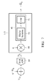
- To extract actual weighting value of the capacitor C8, the digital output signal Do is correlated with the random q and then low-pass filtered. In the embodiment, the low-pass filtering is achieved by integration and average operations. That is, the digital output signal Do is further integrated and divided by M cycles. As shown in
FIG. 7 , in this embodiment the low-pass filter 41 is implemented by a digital accumulator (Digital Accumu.) 70 and a divider (1/M) 71. Thus, we have:
- Assume that the random sequence q is uncorrelated with the analog input signal Vin. The calibrated weighting value of the capacitor C8 is obtained as:

- While the calibrated weighting value Ŵ 8 is obtained, the digital output signal Do can be corrected according to the calibrated weighting value Ŵ 8 as:

- The above calibration process is also performed to the C9,0∼C9,1, C10,0∼C10,3, and C11,0∼C11,7. The corresponding calibrated weighting values are given by:


- After the calibration process of the weighting values of C8, C9,0∼C9,1, C10,0∼C10,3, and C11,0∼C11,7, the digital output signal Do is corrected as:

- While the invention has been described by way of example and in terms of the preferred embodiments, it is to be understood that the invention is not limited to the disclosed embodiments. To the contrary, it is intended to cover various modifications and similar arrangements (as would be apparent to those skilled in the art). Therefore, the scope of the appended claims should be accorded the broadest interpretation so as to encompass all such modifications and similar arrangements.
Claims (15)
- A successive approximation register (SAR) analog to digital converter (ADC) circuit receiving an analog input signal and operating in a sample phase and a conversion phase following the sample phase to generate a digital output signal, comprising:a plurality of capacitors, coupled to a summing node, wherein before the conversion phase, a target capacitor among the plurality of capacitors is coupled to a direct current (DC) voltage and the other capacitors among the plurality of capacitors are coupled to the analog input signal;a comparator having an input terminal coupled to the summing node, wherein in the conversion phase, the comparator performs a comparison operation to a summing voltage at the summing node; anda logic unit having a plurality of weighting values corresponding to the plurality of capacitors respectively and generating the digital output signal according to the weighting values and a comparison result of the comparison operation,wherein the DC voltage has a first voltage level or a second voltage level different from the first voltage level according to a random sequence, andwherein the weighting value of the target capacitor is calibrated according to the digital output signal and the random sequence.
- The SAR ADC circuit as claimed in claim 1, wherein the mean of the random sequence is equal to zero.
- The SAR ADC circuit as claimed in claim 1, further comprising:an extraction and compensation unit receiving the digital output signal,wherein the extraction and compensation unit performs a correlation operation to the digital output signal with the random sequence and further performs a low-pass-filtering operation to the digital output signal to generate a calibrated weighting value, andwherein the extraction and compensation unit corrects the digital output signal based on the weighting value of the target capacitor.
- The SAR ADC circuit as claimed in claim 1, wherein the extraction and compensation unit comprises:a multiplier receiving the digital output signal and performing the correlation operation to the digital output signal and the random sequence; anda low-pass filter, coupled to the multiplier and performing the low-pass-filtering operation to generate the calibrated weighting value.
- The SAR ADC circuit as claimed in claim 4, wherein the low-pass filter is implemented by a digital accumulator and a divider which operate by predetermined cycles to generate the calibrated weighting value.
- The SAR ADC circuit as claimed in claim 1, wherein the random sequence is uncorrelated with the analog input signal.
- A successive approximation register (SAR) analog to digital converter (ADC) circuit receiving an analog input signal and operating in a sample phase and a conversion phase following the sample phase to generate a digital output signal, comprising:a first switch coupled between a first voltage and a summing node;a plurality of capacitors each having a first terminal coupled to the summing node and further having a second terminal;a plurality of second switches, wherein each second switch is coupled between the second terminal of one of the plurality of capacitors and a second voltage;a plurality of switch circuits receiving the analog input signal, wherein each switch circuits is coupled to the second terminal of one of the plurality of capacitors and, before the conversion phase, provides a DC voltage or the analog input signal to the corresponding capacitor;a comparator having an input terminal coupled to the summing node, wherein in the conversion phase, the comparator performs a comparison operation to a summing voltage at the summing node;a logic unit having a plurality of weighting values corresponding to the plurality of capacitors respectively and generating the digital output signal according to the weighting values and a comparison result of the comparison operation; andan extraction and compensation unit receiving the digital output signal,wherein when a target capacitor among the plurality of switch circuits receive the DC voltage from the corresponding switch circuit, the DC voltage has a first voltage level or a second voltage level different from the first voltage level based on a random sequence, andwherein the extraction and compensation unit obtains a calibrated weighting value according to the digital output signal and the random sequence, and the calibrated weighting value serves as the weighting value of the target capacitor.
- The SAR ADC circuit as claimed in claim 7, wherein the mean of the random sequence is equal to zero.
- The SAR ADC circuit as claimed in claim 7,
wherein the extraction and compensation unit performs a correlation operation to the digital output signal with the random sequence and further performs a low-pass-filtering operation to the digital output signal to generate a calibrated weighting value, and
wherein the extraction and compensation unit corrects the digital output signal based on the weighting value of the target capacitor. - The SAR ADC circuit as claimed in claim 7, wherein the extraction and compensation unit comprises:a multiplier receiving the digital output signal and performing the correlation operation to the digital output signal and the random sequence; anda low-pass filter, coupled to the multiplier and performing the low-pass-filtering operation to generate the calibrated weighting value.
- The SAR ADC circuit as claimed in claim 7, wherein the random sequence is uncorrelated with the analog input signal.
- The SAR ADC circuit as claimed in claim 7, wherein each switch circuit comprises:a third switch coupled between the second terminal of the corresponding capacitor and the analog input signal;a fourth switch coupled between the second terminal of the corresponding capacitor and a voltage with the first voltage level; anda fifth switch coupled between the second terminal of the corresponding capacitor and a voltage with the second voltage level,wherein the third switch, the fourth switch, and the fifth switch are not turned on at the same time.
- The SAR ADC circuit as claimed in claim 12, wherein the logic circuit controls the third switch, the fourth switch, and the fifth switch according to whether the weighting value of the corresponding capacitor is to be calibrated.
- The SAR ADC circuit as claimed in claim 13, wherein when the weighting value of the corresponding capacitor is to be calibrated, the logic circuit controls the fourth switch and the fifth switch according to the random sequence.
- The SAR ADC circuit as claimed in claim 12, wherein a polarity of the voltage with the first voltage level is inverse to a polarity of the voltage with the second voltage level.
Applications Claiming Priority (2)
| Application Number | Priority Date | Filing Date | Title |
|---|---|---|---|
| US201562105418P | 2015-01-20 | 2015-01-20 | |
| US14/693,183 US9287891B1 (en) | 2015-01-20 | 2015-04-22 | Successive approximation register analog to digital converters |
Publications (1)
| Publication Number | Publication Date |
|---|---|
| EP3070849A1 true EP3070849A1 (en) | 2016-09-21 |
Family
ID=55450263
Family Applications (1)
| Application Number | Title | Priority Date | Filing Date |
|---|---|---|---|
| EP15170086.1A Withdrawn EP3070849A1 (en) | 2015-01-20 | 2015-06-01 | Successive aproximation register analog to digital converters |
Country Status (3)
| Country | Link |
|---|---|
| US (1) | US9287891B1 (en) |
| EP (1) | EP3070849A1 (en) |
| CN (1) | CN105811976A (en) |
Cited By (1)
| Publication number | Priority date | Publication date | Assignee | Title |
|---|---|---|---|---|
| WO2021133403A1 (en) | 2019-12-27 | 2021-07-01 | Intel Corporation | Analog-to-digital converter and method for calibrating the same, method for calibrating a pipelined analog-to-digital converter, receiver, base station and mobile device |
Families Citing this family (21)
| Publication number | Priority date | Publication date | Assignee | Title |
|---|---|---|---|---|
| KR101501881B1 (en) * | 2014-07-31 | 2015-03-19 | 중앙대학교 산학협력단 | SAR-ADC with spilt dual capacitive array |
| US9385740B2 (en) * | 2014-11-07 | 2016-07-05 | Mediatek Inc. | SAR ADC and method thereof |
| EP3252952B1 (en) * | 2016-05-31 | 2019-01-30 | NXP USA, Inc. | An analogue to digital converter |
| CN106772371A (en) * | 2016-11-21 | 2017-05-31 | 上海卫星工程研究所 | Polarimetric calibration parameter requirements analysis method based on polarimetric SAR interferometry classification application |
| US11372032B2 (en) | 2017-09-27 | 2022-06-28 | Texas Instruments Incorporated | Voltage monitor using a capacitive digital-to-analog converter |
| CN108631780A (en) * | 2017-10-09 | 2018-10-09 | 矽力杰半导体技术(杭州)有限公司 | The method of capacitor array weight calibration |
| US10866269B2 (en) * | 2017-11-16 | 2020-12-15 | Microchip Technology Incorporated | Fast frequency calculator |
| CN107888190B (en) * | 2017-12-01 | 2020-09-25 | 西安电子科技大学 | Successive approximation type analog-digital converter based on asymmetric differential capacitor array |
| US10277244B1 (en) * | 2018-07-26 | 2019-04-30 | Qualcomm Incorporated | Successive approximation register (SAR) analog-to-digital converter (ADC) with passive gain scaling |
| TWI698091B (en) * | 2018-12-12 | 2020-07-01 | 瑞昱半導體股份有限公司 | Successive approximation register analog-to-digital converter and operation method thereof |
| US10778242B2 (en) | 2019-01-11 | 2020-09-15 | Realtek Semiconductor Corporation | Analog-to-digital converter device |
| US10763875B2 (en) * | 2019-01-11 | 2020-09-01 | Realtek Semiconductor Corporation | Switched capacitor circuit and analog-to-digital converter device |
| US10790843B2 (en) | 2019-01-11 | 2020-09-29 | Realtek Semiconductor Corporation | Analog-to-digital converter device |
| US10911059B2 (en) * | 2019-03-13 | 2021-02-02 | Mediatek Inc. | Signal processing system using analog-to-digital converter with digital-to-analog converter circuits operating in different voltage domains and employing mismatch error shaping technique and associated signal processing method |
| CN110535467B (en) * | 2019-07-26 | 2023-03-24 | 中国科学院上海微系统与信息技术研究所 | Capacitor array calibration method and device of stepwise approximation type analog-to-digital conversion device |
| US10742225B1 (en) * | 2019-12-27 | 2020-08-11 | Intel Corporation | n-bit successive approximation register analog-to-digital converter and method for calibrating the same, receiver, base station and mobile device |
| CN111490791B (en) * | 2020-05-13 | 2023-04-07 | 深圳芥子科技有限公司 | Incremental successive approximation analog-to-digital converter |
| US11568915B2 (en) * | 2021-05-10 | 2023-01-31 | Micron Technology, Inc. | Voltage adjustment of memory dies based on weighted feedback |
| EP4125220A1 (en) | 2021-07-28 | 2023-02-01 | Socionext Inc. | Linearity and/or gain in mixed-signal circuitry |
| CN114244371A (en) * | 2021-12-20 | 2022-03-25 | 合肥中感微电子有限公司 | A successive approximation analog-to-digital converter and electronic device |
| CN114726370A (en) * | 2022-04-13 | 2022-07-08 | 中国科学技术大学 | Successive approximation analog-to-digital converter |
Citations (2)
| Publication number | Priority date | Publication date | Assignee | Title |
|---|---|---|---|---|
| US20120001781A1 (en) * | 2010-06-30 | 2012-01-05 | University Of Limerick | Digital Background Calibration System and Method for Successive Approximation (SAR) Analogue to Digital Converter |
| EP2654208A2 (en) * | 2012-04-20 | 2013-10-23 | Linear Technology Corporation | Analog-to-digital converter system and method |
Family Cites Families (7)
| Publication number | Priority date | Publication date | Assignee | Title |
|---|---|---|---|---|
| US8451151B2 (en) * | 2011-08-15 | 2013-05-28 | Himax Technologies Limited | Successive approximation analog to digital converter with capacitor mismatch calibration and method thereof |
| CN102970038B (en) * | 2011-08-31 | 2016-02-03 | 奇景光电股份有限公司 | Approximation analog-to-digital converter for correcting capacitance mismatch and method thereof |
| US8477058B2 (en) * | 2011-10-12 | 2013-07-02 | Ncku Research And Development Foundation | Successive approximation analog to digital converter with a direct switching technique for capacitor array through comparator output and method thereof |
| CN103095300B (en) * | 2011-11-04 | 2015-12-02 | 奇景光电股份有限公司 | Successive approximation analog to digital converter and conversion method |
| TWI501562B (en) * | 2012-10-05 | 2015-09-21 | Univ Nat Chiao Tung | A method to estimate the ratio errors of the capacitors in the digital-to-analog converter of a successive approximation analog digital converter and its application to calibrate the successive approximation analog digital converter |
| TWI497918B (en) * | 2012-12-28 | 2015-08-21 | Ind Tech Res Inst | Analog to digital converter and capacitors weighting evaluating method of digital to analog converter thereof |
| US8981973B2 (en) * | 2013-03-08 | 2015-03-17 | Microchip Technology Incorporated | Successive-approximation-register (SAR) analog-to-digital converter (ADC) attenuation capacitor calibration method and apparatus |
-
2015
- 2015-04-22 US US14/693,183 patent/US9287891B1/en active Active
- 2015-06-01 EP EP15170086.1A patent/EP3070849A1/en not_active Withdrawn
- 2015-09-14 CN CN201510581644.9A patent/CN105811976A/en not_active Withdrawn
Patent Citations (2)
| Publication number | Priority date | Publication date | Assignee | Title |
|---|---|---|---|---|
| US20120001781A1 (en) * | 2010-06-30 | 2012-01-05 | University Of Limerick | Digital Background Calibration System and Method for Successive Approximation (SAR) Analogue to Digital Converter |
| EP2654208A2 (en) * | 2012-04-20 | 2013-10-23 | Linear Technology Corporation | Analog-to-digital converter system and method |
Cited By (3)
| Publication number | Priority date | Publication date | Assignee | Title |
|---|---|---|---|---|
| WO2021133403A1 (en) | 2019-12-27 | 2021-07-01 | Intel Corporation | Analog-to-digital converter and method for calibrating the same, method for calibrating a pipelined analog-to-digital converter, receiver, base station and mobile device |
| EP4082113A4 (en) * | 2019-12-27 | 2023-11-08 | Intel Corporation | Analog-to-digital converter and method for calibrating the same, method for calibrating a pipelined analog-to-digital converter, receiver, base station and mobile device |
| US12063050B2 (en) | 2019-12-27 | 2024-08-13 | Intel Corporation | Analog-to-digital converter and method for calibrating the same, method for calibrating a pipelined analog-to-digital converter, receiver, base station and mobile device |
Also Published As
| Publication number | Publication date |
|---|---|
| CN105811976A (en) | 2016-07-27 |
| US9287891B1 (en) | 2016-03-15 |
Similar Documents
| Publication | Publication Date | Title |
|---|---|---|
| US9287891B1 (en) | Successive approximation register analog to digital converters | |
| CN112202448B (en) | Successive approximation type analog-to-digital converter, calibration method thereof and electronic equipment | |
| US10581443B2 (en) | Method and apparatus for offset correction in SAR ADC with reduced capacitor array DAC | |
| US8907826B2 (en) | Method for estimating capacitance weight errors and successive approximation analog to digital converter using the same | |
| US8902092B2 (en) | Analog-digital conversion circuit and method | |
| US9362938B2 (en) | Error measurement and calibration of analog to digital converters | |
| US10461767B1 (en) | Successive approximation register (SAR) analog to digital converter (ADC) with switchable reference voltage | |
| US11070225B2 (en) | Successive approximation register (SAR) analog to digital converter (ADC) with overlapping reference voltage ranges | |
| US20110133963A1 (en) | Successive aproximation A/D Converter | |
| JP2009118488A (en) | DA converter and AD converter | |
| US20100156689A1 (en) | A-d convert apparatus, d-a convert apparatus and adjustment method | |
| US9013345B2 (en) | Successive approximation AD converter and successive approximation AD conversion method | |
| CN100499376C (en) | Analog-to-digital converter capable of operating in two different modes | |
| CN102970038B (en) | Approximation analog-to-digital converter for correcting capacitance mismatch and method thereof | |
| US11133813B2 (en) | Analog to digital converter device and noise shaping digital slope analog to digital converter circuitry | |
| US9509327B2 (en) | A/D converter and A/D converter calibrating method | |
| US10491232B1 (en) | Successive approximation register (SAR) analog to digital converter (ADC) dynamic range extension | |
| US10897261B1 (en) | Analog-to-digital converter with a supplementary digital-to-analog converter for offset and gain error measurements | |
| CN118367935A (en) | Analog-to-digital conversion circuit, analog-to-digital conversion method, chip and electronic equipment | |
| JP6131102B2 (en) | Successive comparison type A / D converter and driving method thereof | |
| US9413371B1 (en) | ADC and analog-to-digital converting method | |
| US10735017B2 (en) | Efficient successive approximation register analog to digital converter | |
| US12328128B2 (en) | Sampling circuit, analog-to-digital converter circuit, and semiconductor integrated circuit | |
| US20260031830A1 (en) | Analog to digital converter, method and circuit for detecting defect therein | |
| US20110148684A1 (en) | Successive approximation analog-to-digital converter |
Legal Events
| Date | Code | Title | Description |
|---|---|---|---|
| PUAI | Public reference made under article 153(3) epc to a published international application that has entered the european phase |
Free format text: ORIGINAL CODE: 0009012 |
|
| AK | Designated contracting states |
Kind code of ref document: A1 Designated state(s): AL AT BE BG CH CY CZ DE DK EE ES FI FR GB GR HR HU IE IS IT LI LT LU LV MC MK MT NL NO PL PT RO RS SE SI SK SM TR |
|
| AX | Request for extension of the european patent |
Extension state: BA ME |
|
| STAA | Information on the status of an ep patent application or granted ep patent |
Free format text: STATUS: REQUEST FOR EXAMINATION WAS MADE |
|
| 17P | Request for examination filed |
Effective date: 20170321 |
|
| RBV | Designated contracting states (corrected) |
Designated state(s): AL AT BE BG CH CY CZ DE DK EE ES FI FR GB GR HR HU IE IS IT LI LT LU LV MC MK MT NL NO PL PT RO RS SE SI SK SM TR |
|
| STAA | Information on the status of an ep patent application or granted ep patent |
Free format text: STATUS: EXAMINATION IS IN PROGRESS |
|
| 17Q | First examination report despatched |
Effective date: 20190221 |
|
| STAA | Information on the status of an ep patent application or granted ep patent |
Free format text: STATUS: THE APPLICATION HAS BEEN WITHDRAWN |
|
| 18W | Application withdrawn |
Effective date: 20190425 |