EP3069303B1 - Carte a puce avec cadre de couplage et procede d'augmentation de la distance d'activation d'un module de puce transpondeur - Google Patents
Carte a puce avec cadre de couplage et procede d'augmentation de la distance d'activation d'un module de puce transpondeur Download PDFInfo
- Publication number
- EP3069303B1 EP3069303B1 EP14777025.9A EP14777025A EP3069303B1 EP 3069303 B1 EP3069303 B1 EP 3069303B1 EP 14777025 A EP14777025 A EP 14777025A EP 3069303 B1 EP3069303 B1 EP 3069303B1
- Authority
- EP
- European Patent Office
- Prior art keywords
- chip module
- transponder chip
- metal layer
- tcm
- coupling frame
- Prior art date
- Legal status (The legal status is an assumption and is not a legal conclusion. Google has not performed a legal analysis and makes no representation as to the accuracy of the status listed.)
- Active
Links
- 230000008878 coupling Effects 0.000 title claims description 332
- 238000010168 coupling process Methods 0.000 title claims description 332
- 238000005859 coupling reaction Methods 0.000 title claims description 332
- 230000004913 activation Effects 0.000 title claims description 53
- 238000000034 method Methods 0.000 title claims description 16
- 230000001965 increasing effect Effects 0.000 title description 11
- 229910052751 metal Inorganic materials 0.000 claims description 285
- 239000002184 metal Substances 0.000 claims description 285
- 239000000463 material Substances 0.000 claims description 31
- 239000004020 conductor Substances 0.000 claims description 24
- 230000003014 reinforcing effect Effects 0.000 claims description 24
- RYGMFSIKBFXOCR-UHFFFAOYSA-N Copper Chemical compound [Cu] RYGMFSIKBFXOCR-UHFFFAOYSA-N 0.000 claims description 17
- 229910052782 aluminium Inorganic materials 0.000 claims description 17
- XAGFODPZIPBFFR-UHFFFAOYSA-N aluminium Chemical compound [Al] XAGFODPZIPBFFR-UHFFFAOYSA-N 0.000 claims description 17
- 229910052802 copper Inorganic materials 0.000 claims description 16
- 239000010949 copper Substances 0.000 claims description 16
- WFKWXMTUELFFGS-UHFFFAOYSA-N tungsten Chemical compound [W] WFKWXMTUELFFGS-UHFFFAOYSA-N 0.000 claims description 16
- 229910052721 tungsten Inorganic materials 0.000 claims description 16
- 239000010937 tungsten Substances 0.000 claims description 16
- OKTJSMMVPCPJKN-UHFFFAOYSA-N Carbon Chemical compound [C] OKTJSMMVPCPJKN-UHFFFAOYSA-N 0.000 claims description 14
- RTAQQCXQSZGOHL-UHFFFAOYSA-N Titanium Chemical compound [Ti] RTAQQCXQSZGOHL-UHFFFAOYSA-N 0.000 claims description 12
- 239000010936 titanium Substances 0.000 claims description 12
- 229910052719 titanium Inorganic materials 0.000 claims description 12
- BQCADISMDOOEFD-UHFFFAOYSA-N Silver Chemical compound [Ag] BQCADISMDOOEFD-UHFFFAOYSA-N 0.000 claims description 10
- 239000010935 stainless steel Substances 0.000 claims description 9
- 229910001220 stainless steel Inorganic materials 0.000 claims description 9
- 229910001369 Brass Inorganic materials 0.000 claims description 7
- 239000010951 brass Substances 0.000 claims description 7
- 229910052799 carbon Inorganic materials 0.000 claims description 6
- 238000004049 embossing Methods 0.000 claims description 6
- 239000003822 epoxy resin Substances 0.000 claims description 6
- 229920000647 polyepoxide Polymers 0.000 claims description 6
- 239000002042 Silver nanowire Substances 0.000 claims description 5
- 229910021389 graphene Inorganic materials 0.000 claims description 5
- 229910052709 silver Inorganic materials 0.000 claims description 5
- 239000004332 silver Substances 0.000 claims description 5
- 230000002708 enhancing effect Effects 0.000 claims description 4
- 230000005611 electricity Effects 0.000 claims description 3
- 230000008569 process Effects 0.000 claims description 3
- 238000007650 screen-printing Methods 0.000 claims description 3
- 239000002952 polymeric resin Substances 0.000 claims description 2
- 229920003002 synthetic resin Polymers 0.000 claims description 2
- 238000007740 vapor deposition Methods 0.000 claims description 2
- 239000010410 layer Substances 0.000 description 119
- 239000011888 foil Substances 0.000 description 58
- 238000010586 diagram Methods 0.000 description 25
- SPNQRCTZKIBOAX-UHFFFAOYSA-N Butralin Chemical compound CCC(C)NC1=C([N+]([O-])=O)C=C(C(C)(C)C)C=C1[N+]([O-])=O SPNQRCTZKIBOAX-UHFFFAOYSA-N 0.000 description 24
- 229920003023 plastic Polymers 0.000 description 21
- 239000004033 plastic Substances 0.000 description 21
- 239000000758 substrate Substances 0.000 description 16
- 230000006870 function Effects 0.000 description 15
- 230000005672 electromagnetic field Effects 0.000 description 11
- 238000010329 laser etching Methods 0.000 description 11
- 230000009977 dual effect Effects 0.000 description 8
- 238000004891 communication Methods 0.000 description 7
- 229910001092 metal group alloy Inorganic materials 0.000 description 7
- 239000004800 polyvinyl chloride Substances 0.000 description 7
- 239000000945 filler Substances 0.000 description 6
- 230000004907 flux Effects 0.000 description 6
- 229920000915 polyvinyl chloride Polymers 0.000 description 6
- 229920005989 resin Polymers 0.000 description 6
- 239000011347 resin Substances 0.000 description 6
- 238000000926 separation method Methods 0.000 description 6
- 239000011800 void material Substances 0.000 description 6
- 230000008901 benefit Effects 0.000 description 5
- 238000005253 cladding Methods 0.000 description 5
- 239000002131 composite material Substances 0.000 description 5
- 230000000670 limiting effect Effects 0.000 description 5
- 239000004411 aluminium Substances 0.000 description 4
- 238000010276 construction Methods 0.000 description 4
- 238000013461 design Methods 0.000 description 4
- 239000010408 film Substances 0.000 description 4
- 150000002739 metals Chemical class 0.000 description 4
- 230000002441 reversible effect Effects 0.000 description 4
- 239000000126 substance Substances 0.000 description 4
- 229910000831 Steel Inorganic materials 0.000 description 3
- 238000005452 bending Methods 0.000 description 3
- 238000003486 chemical etching Methods 0.000 description 3
- 238000002474 experimental method Methods 0.000 description 3
- 238000003306 harvesting Methods 0.000 description 3
- 238000000608 laser ablation Methods 0.000 description 3
- 239000012811 non-conductive material Substances 0.000 description 3
- 230000002829 reductive effect Effects 0.000 description 3
- 239000010959 steel Substances 0.000 description 3
- 239000004593 Epoxy Substances 0.000 description 2
- 239000012790 adhesive layer Substances 0.000 description 2
- 230000002411 adverse Effects 0.000 description 2
- 229910045601 alloy Inorganic materials 0.000 description 2
- 239000000956 alloy Substances 0.000 description 2
- 230000015572 biosynthetic process Effects 0.000 description 2
- 238000000576 coating method Methods 0.000 description 2
- 239000011231 conductive filler Substances 0.000 description 2
- 230000008021 deposition Effects 0.000 description 2
- 230000000694 effects Effects 0.000 description 2
- 229910002804 graphite Inorganic materials 0.000 description 2
- 239000010439 graphite Substances 0.000 description 2
- 230000001976 improved effect Effects 0.000 description 2
- 230000006872 improvement Effects 0.000 description 2
- 238000011835 investigation Methods 0.000 description 2
- 239000006249 magnetic particle Substances 0.000 description 2
- 238000003701 mechanical milling Methods 0.000 description 2
- 239000002923 metal particle Substances 0.000 description 2
- 230000004048 modification Effects 0.000 description 2
- 238000012986 modification Methods 0.000 description 2
- 239000002086 nanomaterial Substances 0.000 description 2
- 230000003647 oxidation Effects 0.000 description 2
- 238000007254 oxidation reaction Methods 0.000 description 2
- 238000007747 plating Methods 0.000 description 2
- 229920000515 polycarbonate Polymers 0.000 description 2
- 239000004417 polycarbonate Substances 0.000 description 2
- 229920000139 polyethylene terephthalate Polymers 0.000 description 2
- 229920000642 polymer Polymers 0.000 description 2
- 229920002994 synthetic fiber Polymers 0.000 description 2
- 230000003313 weakening effect Effects 0.000 description 2
- 229910000859 α-Fe Inorganic materials 0.000 description 2
- 229920001634 Copolyester Polymers 0.000 description 1
- 229910000570 Cupronickel Inorganic materials 0.000 description 1
- XUIMIQQOPSSXEZ-UHFFFAOYSA-N Silicon Chemical compound [Si] XUIMIQQOPSSXEZ-UHFFFAOYSA-N 0.000 description 1
- 238000010521 absorption reaction Methods 0.000 description 1
- 239000002253 acid Substances 0.000 description 1
- 230000009471 action Effects 0.000 description 1
- 239000000853 adhesive Substances 0.000 description 1
- 230000001070 adhesive effect Effects 0.000 description 1
- 239000002390 adhesive tape Substances 0.000 description 1
- PNEYBMLMFCGWSK-UHFFFAOYSA-N aluminium oxide Inorganic materials [O-2].[O-2].[O-2].[Al+3].[Al+3] PNEYBMLMFCGWSK-UHFFFAOYSA-N 0.000 description 1
- 238000000137 annealing Methods 0.000 description 1
- 230000005540 biological transmission Effects 0.000 description 1
- -1 body Substances 0.000 description 1
- 229910002091 carbon monoxide Inorganic materials 0.000 description 1
- 239000002041 carbon nanotube Substances 0.000 description 1
- 229910021393 carbon nanotube Inorganic materials 0.000 description 1
- 239000000969 carrier Substances 0.000 description 1
- 238000007385 chemical modification Methods 0.000 description 1
- 230000000295 complement effect Effects 0.000 description 1
- 239000012141 concentrate Substances 0.000 description 1
- 239000011370 conductive nanoparticle Substances 0.000 description 1
- 239000011889 copper foil Substances 0.000 description 1
- 238000005520 cutting process Methods 0.000 description 1
- 230000003247 decreasing effect Effects 0.000 description 1
- 230000001687 destabilization Effects 0.000 description 1
- 230000000368 destabilizing effect Effects 0.000 description 1
- 239000003989 dielectric material Substances 0.000 description 1
- 230000002500 effect on skin Effects 0.000 description 1
- 230000005670 electromagnetic radiation Effects 0.000 description 1
- 238000009713 electroplating Methods 0.000 description 1
- 238000005530 etching Methods 0.000 description 1
- 230000002349 favourable effect Effects 0.000 description 1
- 238000011049 filling Methods 0.000 description 1
- 238000009472 formulation Methods 0.000 description 1
- 239000011521 glass Substances 0.000 description 1
- 239000003292 glue Substances 0.000 description 1
- 239000007943 implant Substances 0.000 description 1
- AMGQUBHHOARCQH-UHFFFAOYSA-N indium;oxotin Chemical compound [In].[Sn]=O AMGQUBHHOARCQH-UHFFFAOYSA-N 0.000 description 1
- 238000009434 installation Methods 0.000 description 1
- 230000003993 interaction Effects 0.000 description 1
- 230000002452 interceptive effect Effects 0.000 description 1
- 238000002955 isolation Methods 0.000 description 1
- MOYKHGMNXAOIAT-JGWLITMVSA-N isosorbide dinitrate Chemical compound [O-][N+](=O)O[C@H]1CO[C@@H]2[C@H](O[N+](=O)[O-])CO[C@@H]21 MOYKHGMNXAOIAT-JGWLITMVSA-N 0.000 description 1
- 238000003475 lamination Methods 0.000 description 1
- 238000010297 mechanical methods and process Methods 0.000 description 1
- 230000005226 mechanical processes and functions Effects 0.000 description 1
- 239000002905 metal composite material Substances 0.000 description 1
- 239000002082 metal nanoparticle Substances 0.000 description 1
- 230000000116 mitigating effect Effects 0.000 description 1
- 239000000203 mixture Substances 0.000 description 1
- 239000002070 nanowire Substances 0.000 description 1
- 230000003287 optical effect Effects 0.000 description 1
- TWNQGVIAIRXVLR-UHFFFAOYSA-N oxo(oxoalumanyloxy)alumane Chemical compound O=[Al]O[Al]=O TWNQGVIAIRXVLR-UHFFFAOYSA-N 0.000 description 1
- 239000000123 paper Substances 0.000 description 1
- 230000036961 partial effect Effects 0.000 description 1
- 230000000149 penetrating effect Effects 0.000 description 1
- 230000035515 penetration Effects 0.000 description 1
- 230000002093 peripheral effect Effects 0.000 description 1
- 229920005644 polyethylene terephthalate glycol copolymer Polymers 0.000 description 1
- 238000012545 processing Methods 0.000 description 1
- 239000002990 reinforced plastic Substances 0.000 description 1
- 230000002040 relaxant effect Effects 0.000 description 1
- 238000009877 rendering Methods 0.000 description 1
- 238000012216 screening Methods 0.000 description 1
- 239000004065 semiconductor Substances 0.000 description 1
- 229910052710 silicon Inorganic materials 0.000 description 1
- 239000010703 silicon Substances 0.000 description 1
- 229910000679 solder Inorganic materials 0.000 description 1
- 239000007787 solid Substances 0.000 description 1
- 239000007858 starting material Substances 0.000 description 1
- 229910052715 tantalum Inorganic materials 0.000 description 1
- GUVRBAGPIYLISA-UHFFFAOYSA-N tantalum atom Chemical compound [Ta] GUVRBAGPIYLISA-UHFFFAOYSA-N 0.000 description 1
- 238000012360 testing method Methods 0.000 description 1
- 239000010409 thin film Substances 0.000 description 1
- 238000002834 transmittance Methods 0.000 description 1
- 230000000007 visual effect Effects 0.000 description 1
- 238000003466 welding Methods 0.000 description 1
- 238000004804 winding Methods 0.000 description 1
Images


Classifications
-
- G—PHYSICS
- G06—COMPUTING; CALCULATING OR COUNTING
- G06K—GRAPHICAL DATA READING; PRESENTATION OF DATA; RECORD CARRIERS; HANDLING RECORD CARRIERS
- G06K19/00—Record carriers for use with machines and with at least a part designed to carry digital markings
- G06K19/06—Record carriers for use with machines and with at least a part designed to carry digital markings characterised by the kind of the digital marking, e.g. shape, nature, code
- G06K19/067—Record carriers with conductive marks, printed circuits or semiconductor circuit elements, e.g. credit or identity cards also with resonating or responding marks without active components
- G06K19/07—Record carriers with conductive marks, printed circuits or semiconductor circuit elements, e.g. credit or identity cards also with resonating or responding marks without active components with integrated circuit chips
- G06K19/077—Constructional details, e.g. mounting of circuits in the carrier
- G06K19/0772—Physical layout of the record carrier
- G06K19/07728—Physical layout of the record carrier the record carrier comprising means for protection against impact or bending, e.g. protective shells or stress-absorbing layers around the integrated circuit
-
- G—PHYSICS
- G06—COMPUTING; CALCULATING OR COUNTING
- G06K—GRAPHICAL DATA READING; PRESENTATION OF DATA; RECORD CARRIERS; HANDLING RECORD CARRIERS
- G06K19/00—Record carriers for use with machines and with at least a part designed to carry digital markings
- G06K19/06—Record carriers for use with machines and with at least a part designed to carry digital markings characterised by the kind of the digital marking, e.g. shape, nature, code
- G06K19/067—Record carriers with conductive marks, printed circuits or semiconductor circuit elements, e.g. credit or identity cards also with resonating or responding marks without active components
- G06K19/07—Record carriers with conductive marks, printed circuits or semiconductor circuit elements, e.g. credit or identity cards also with resonating or responding marks without active components with integrated circuit chips
- G06K19/077—Constructional details, e.g. mounting of circuits in the carrier
- G06K19/0772—Physical layout of the record carrier
- G06K19/07722—Physical layout of the record carrier the record carrier being multilayered, e.g. laminated sheets
Definitions
- the smartcard (or payment cards, secure documents, access control cards, electronic tickets, small form factor tags, data carriers, mobile payment devices and the like), operating at least in a contactless mode (ISO 14443 and NFC/ISO 15693).
- the smartcard (or smart card) comprises a card body (CB) comprising at least a metal layer, and a transponder chip module (TCM) comprising a dual interface RFID chip and an antenna.
- CB card body
- TCM transponder chip module
- a prior art dual interface (DI or DIF) smartcard (or smart card; SC) may generally comprise:
- the antenna module “AM” may generally comprise a "DI” RFID chip (bare, unpackaged silicon die) or chip module (a die with leadframe, interposer, carrier or the like) - either of which may be referred to as "CM” - mounted to a module tape "MT".
- the RFID chip (CM) may be mounted on a module tape (MT), typically having 6 or 8 contact pads (CP) for interfacing with a contact reader in a contact mode (ISO 7816).
- a module antenna "MA” may be disposed on the module tape MT for implementing a contactless interface, such as ISO 14443 and NFC/ISO 15693.
- Contact pads "CP” may be disposed on the module tape MT for implementing a contact interface, such as ISO 7816.
- the contact pads (CP) may or may not be perforated.
- the module tape MT may comprise a pattern of interconnects (conductive traces and pads) to which the RFID chip CM and contact pads CP may be connected.
- the module antenna MA may be connected, indirectly, via some of the interconnects to the chip CM, or may be directly connected to bond pads BP on the RFID chip CM.
- the module antenna MA may comprise several turns of wire, such as 112 micron diameter insulated wire. Reference may be made to US 6,378,774 (2002, Toppan ), for example FIGs. 12A, B thereof.
- the module antenna (MA) may comprise a chemically-etched, planar module antenna MA with planar tracks surrounding the chip (CM). Reference may be made to US 8,100,337 (2012, SPS ), for example FIG. 3 thereof.
- the antenna module “AM” may comprise a module antenna (MA) which has been formed from a wire wound coil which is arranged on or mounted to the module tape (MT), or may comprise a planar antenna structure (AS) which is etched (chemically etched or laser etched, from a foil on the module tape MT) to have a number of tracks separated by spaces. Generally, with laser etching, the spacing between tracks can be made smaller (such as 25 ⁇ m) than with chemical etching (such as 100 ⁇ m).
- MA module antenna
- AS planar antenna structure
- a module antenna (MA) connected to an RFID chip (CM) may be referred to as a "transponder”.
- a transponder is a “passive” transponder which does not have its own power source (e.g., battery), but rather which harvests power from an external reader (interrogator).
- the activation distance of an antenna module (AM) having a chemically-etched module antenna (MA), without a booster antenna (BA) in the card body (CB), may be only a few millimeters.
- the activation distance of an antenna module (AM) having a laser-etched antenna structure (LES), without a booster antenna (BA) in the card body (CB) may be 15 - 20 mm.
- the activation distance of antenna module (AM) with a booster antenna (BA) in the card body (CB) is typically four centimeters to meet ISO and EMV standards.
- antenna modules may require a booster antenna (BA) in a card body (CB) to achieve these distances.
- antenna modules (AM) incorporating a laser-etched antenna structure (LES) are able to operate without a booster antenna (BA) in the card body (CB), and may be referred to as transponder chip modules (TCM).
- TCM transponder chip module
- TCM transponder IC module
- the antenna module AM (or transponder chip module TCM) may be generally rectangular, having four sides, and measuring approximately 8mm ⁇ 11mm for a 6 contact module and 11mm ⁇ 13mm for an 8 contact module.
- the transponder chip module (TCM) may be round, elliptical, or other non-rectangular shape.
- the transponder chip module (TCM) may be powered by RF from an external RFID reader, and may also communicate by RF with the external RFID reader.
- An “activation distance” may refer to a distance at which the transponder chip module TCM may harvest sufficient energy from the RFID reader to commence operation.
- a "read/write distance” may refer to a distance at which the transponder chip module TCM may communicate reliably with the external RFID reader.
- the card body CB - which may be referred to as a substrate, or an inlay substrate - may generally comprise one or more layers of material such as Polyvinyl Chloride (PVC), Polycarbonate (PC), PET-G (Polyethylene Terephtalate Glycol-modified), Copolyester (Tritan), Teslin TM , synthetic paper, paper and the like.
- PVC Polyvinyl Chloride
- PC Polycarbonate
- PET-G Polyethylene Terephtalate Glycol-modified
- Copolyester Tritan
- Teslin TM synthetic paper, paper and the like.
- the card body CB may be generally rectangular, measuring approximately 54 mm ⁇ 86 mm (refer to ISO/IEC 7810), having a thickness of approximately 300 ⁇ m thick when referred to as an inlay substrate or 760 ⁇ m when referred to as a smartcard.
- the card body CB is typically significantly (such as 30 times) larger than the antenna module AM
- the booster antenna BA may generally comprise a relatively large winding which may be referred to as a card antenna CA component (or portion) having a number of turns disposed in a peripheral area of the card body CB, and a relatively small coupler coil (or coupler antenna) CC component (or portion) having a number of turns disposed at a coupling area of the card body CB corresponding to the location of the antenna module AM
- the card antenna CA and coupler coil CC may comprise wire mounted to (embedded in) the card body CB using an ultrasonic tool comprising a sonotrode and a capillary. See, for example US 6,698,089 and US 6,233,818 .
- the wire may be non-insulated, insulated, or self-bonding wire, having an exemplary diameter in the range of approximately 50 - 112 ⁇ m.
- SC smartcards
- BA booster antennas
- Metallized smartcards may have a faceplate or layer of metal extending over nearly the entire area of the card (except for an opening for the antenna module (AM)), and some smartcards may be made largely of metal.
- the presence of such a metal layer or mass in the smartcard may tend to attenuate contactless communication (e.g., ISO 14443, ISO 15693) between the smartcard and an external reader.
- the contact pads themselves may also tend to attenuate contactless communication.
- metallized smartcards may often function in a contact mode (e.g., ISO 7816) only.
- WO 2013/110625 A1 discloses a metallized smartcard having a booster antenna with coupler coil in its card boy and a metallized face plate including a window opening for the antenna module. There is a gap between the periphery of the window opening and the antenna module. Performance of the card may be enhanced by making the window opening substantially larger than the antenna module.
- Foil composite cards and metal cards may be disclosed in ...
- a conductive "compensation loop" CL may be disposed behind the booster antenna BA, extending around the periphery of the card body CB.
- the compensation loop CL may be an open loop having two free ends, and a gap ("gap") therebetween.
- the compensation loop CL may be made of copper cladding.
- Some other objects may include relaxing performance constraints on the booster antenna (BA) of the smart card (SC), including the possibility of eliminating the booster antenna (BA) altogether.
- a conductive coupling frame having two ends, forming an open loop or discontinuous metal layer, disposed surrounding and closely adjacent a transponder chip module (TCM), and substantially coplanar with an antenna structure (AS, CES, LES) in the transponder chip module (TCM).
- the coupling frame (CF) may be thick enough to be non-transparent to RF at frequencies of interest.
- a switch may be provided to connect ends of the coupling frame (CF) across the slit (S).
- a reinforcing structure may be provided to stabilize a card body.
- the transponder chip module (TCM) may comprise a laser-etched antenna structure (LES), a chemical-etched antenna structure (CES) and a non-perforated contact pad (CP) arrangement.
- a coupling frame (CF) may be incorporated onto the module tape (MT) for a transponder chip module (TCM).
- a smartcard comprises an electrically-conductive layer, referred to herein as a "coupling frame" (CF) disposed in the card body (CB). It may be disposed around at least two sides (or 180°) of a transponder chip module (TCM) so as to be in close proximity with the module antenna (MA) in the transponder chip module (TCM).
- the coupling frame (CF) may at least partially surround the transponder chip module (TCM), such as surrounding two sides (or 180°) or three sides (or 270°) of the transponder chip module (TCM), particularly the antenna structure (AS) of the transponder chip module (TCM). This includes “at least" two sides and "at least" three sides.
- the coupling frame (CF) may nearly completely surround the transponder chip module (TCM), such as all four sides (or 360°) thereof, minus a slit (S).
- the slit (S) may be very small, such as 50 ⁇ m. (Such a small (50 ⁇ m) slit (S) may correspond to a fraction of a percent of the perimeter of the transponder chip module (TCM) or module opening (MO), or less than 1°.)
- the module antenna (MA) may comprise an antenna structure (AS) which has been etched from a conductive layer or foil to have a conductor having two ends and arranged in a spiral pattern which has a number (such as 10-12) of turns (which may be referred to as "tracks"), separated by spaces.
- An end portion of an antenna structure (AS) may also comprise of a quarter, half or three quarter turn (fractions of turns).
- a coupling frame (CF) surrounding all four sides (nearly 360°) of the transponder chip module (TCM) may be provided with a module opening (MO) for accommodating the transponder chip module (TCM), and is provided with a slit (or slot, or cut-out, or gap) extending from the module opening (MO) to the perimeter of the coupling frame (CF).
- the slit ensures that the coupling frame (CF) is an "open loop" having two ends.
- a switch (SW) may be incorporated into the card body to connect the ends of the coupling frame (CF) together, so that it is not an open loop.
- the coupling frame may comprise a conductive layer, a metallized layer, a metal layer or overlapping metal layers, each layer at least partially surrounding the transponder chip module (TCM) and (in aggregate, in the case of two or more conductive layers) covering at least a substantial area of the card body (CB) for coupling with an external contactless reader.
- TCM transponder chip module
- CB card body
- the coupling frame may comprise one or more discontinuous layers of conductive material in the form of a perforated metal mesh or a wireframe metal mesh, or other discontinuous surface (including embedded ribbon conductor) to avoid electrostatic discharge (ESD) problems.
- ESD electrostatic discharge
- a coupling frame (CF) with a cut-out (module opening MO) to accept the transponder chip module (TCM) may be positioned in or on the card body to partially surround at close proximity to a laser-etched antenna structure (LES) of the transponder chip module (TCM).
- CF coupling frame
- LES laser-etched antenna structure
- the coupling frames disclosed herein may be formed from layers of various metals (such as copper, aluminum (aluminium), brass, titanium, tungsten, stainless steel, silver, graphene, silver nanowires, conductive carbon ink), and may be in the form of ribbon cable, or the like, which could be hot stamped into a layer of the card.
- various metals such as copper, aluminum (aluminium), brass, titanium, tungsten, stainless steel, silver, graphene, silver nanowires, conductive carbon ink
- the transponder chip module comprises an RFID (radio frequency identification) chip or chip module (either of which may be referred to as "CM”) and an etched (typically planar) antenna structure formed as a flat rectangular spiral having a number (such as 10-12) of conductive tracks separated by spaces.
- CM radio frequency identification
- etched typically planar antenna structure formed as a flat rectangular spiral having a number (such as 10-12) of conductive tracks separated by spaces.
- the spaces between adjacent tracks can be less than 100 ⁇ m, less than 75 ⁇ m, less than 50 ⁇ m and less than 25 ⁇ m.
- the tracks may typically have a width of 100 ⁇ m.
- Laser-etching an antenna structure or structures underneath and surrounding a chip (CM) mounted on a module tape (MT) may improve the overall electrical parameters of the antenna.
- a coupling frame at least partially surrounding a transponder chip module (TCM) and residing substantially on the same plane as the laser-etched antenna structure (LES) in a card body, document or tag, without creating a closed circuit around the transponder chip module (TCM) by leaving at least one space or gap as an open circuit such as a cut-out, slit or slot in the coupling frame (CF), may further increase the amplitude of the resonance curve of the transponder chip module (TCM) with minimal frequency shift when interrogated by a reader.
- TCM transponder chip module
- LES laser-etched antenna structure
- the activation distance of a transponder chip module (TCM) with a coupling frame (CF) may be substantially increased by at least a factor of 1.5, as opposed to the performance of a transponder chip module (TCM) without a coupling frame (CF).
- Activation distances of at least 2cm, including up to 3cm and up to 4cm may be achieved using a transponder chip module (TCM) having a laser-etched antenna structure (LES) in conjunction with a coupling frame (CF) in (or comprising most of) the card body (CB).
- TCM transponder chip module
- LES laser-etched antenna structure
- Metal cards or composite metal cards in ISO card format(s), having a module opening (MO) for accommodating a transponder chip module (TCM) are provided with a slit in the metal, in the manner of the coupling frame (CF) disclosed herein, to break the conductive path and create an open circuit (open loop) conductive structure surrounding the transponder chip module (TCM), thereby increasing the communication distance (e.g., activation distance, Read/Write distance, and the like) between an external reader and a smartcard with a transponder chip module (TCM).
- the slit can be filled or plugged with a non-conductive medium.
- the metal card or metal slug in a card body acting as the coupling frame can be made from materials such as copper, aluminum, tungsten, stainless steel, brass, titanium or a combination thereof.
- Holographic metal foils which may be transparent to high frequency electromagnetic waves and do not impair or influence the performance of a transponder chip module, may be implanted in a metal foil card because the thickness of the metal is significantly lower than the skin depth of the metal at a frequency of interest, such as 13.56 MHz, or more generally 10 - 30 MHz.
- Security features, logos and embossed characters may be engraved, etched or stamped into a metal layer of suitable thickness to perform the function of a coupling frame (CF).
- CF coupling frame
- the invention relates broadly to RFID transponders which are able to transmit data to and receive data from an external reader.
- Such transponders may generally fall into two categories - “active” and “passive”.
- Active transponders have an internal power source, such as a battery.
- Passive transponders are powered by (harvest power from) the external reader. Due to the lack of their own power source, several factors may influence the successful operation of a passive transponder, some of which are addressed herein. For example, the distance at which a passive transponder may be activated (powered up by) and communicate reliably (read/write) with the external reader may be very limited. Consequently, smart cards (SC) comprising passive transponders have typically required booster antennas (BA) in the card body (CB).
- BA booster antennas
- passive RFID transponders comprising (passive) transponder chip modules (TCM) are discussed, and unless otherwise specified, all embodiments are directed to passive RFID transponders and transponder chip modules (TCM).
- Passive RFID transponders and transponder chip modules (TCM) disposed in smart cards (SC) (including metal smart cards) and capable of operating in a contactless mode without requiring a booster antenna (BA) are disclosed herein.
- a conductive coupling frame has two ends, forms an open loop, may be disposed surrounding and closely adjacent a transponder chip module (TCM), and may be substantially coplanar with an antenna structure (AS, LES) in the transponder chip module (TCM).
- a metal card body MB
- MMB metal card body
- S slit
- the coupling frame (CF) may be thick enough to be non-transparent (opaque) to RF at frequencies of interest.
- a switch may be provided to connect ends of the coupling frame (CF) across the slit (S).
- the transponder chip module (TCM) may comprise a laser-etched antenna structure (LES) and a non-perforated contact pad (CP) arrangement.
- a smartcard comprises: a metal layer (ML); and an opening (MO) in the metal layer for receiving a transponder chip module (TCM); characterized by: a discontinuity comprising a slit (S) or a non-conductive stripe (NCS), in the metal layer (ML), extending from the opening to a periphery of the metal layer, whereby the metal layer (ML) comprises an open-loop coupling frame (CF) having two ends.
- the coupling frame may be disposed closely adjacent to the transponder chip module when the transponder chip module is disposed in the opening. A portion of the coupling frame (CF) overlaps a portion of an antenna structure (AS) in the transponder chip module (TCM).
- the coupling frame may extend over substantially the entire area of the smartcard.
- the metal layer may comprise a metal card body (MCB) of a metal smartcard.
- the slit may extend completely through the metal layer.
- the slit may extend only partially through the metal layer, and remaining material of the metal layer below the slit has a thickness below a transparency threshold for the metal layer.
- the slit may have a width which is smaller than the opening.
- the slit may be at least partially filled with an electrically non-conducting material selected from the group consisting of polymer and epoxy resin, reinforced epoxy resin.
- a reinforcing structure (RS) disposed at a location of the slit (S) to reinforce the metal layer (ML).
- the metal layer may be substantially coplanar with an antenna structure (AS) in the transponder chip module.
- the metal layer may comprise a material having a thickness greater than a transparency threshold for absorbing electromagnetic waves at a frequency of interest; may have a thickness greater than a skin depth for conducting electricity at a frequency of interest; has a thickness greater than 1 ⁇ m; may have a thickness greater than 30 ⁇ m; and may have a thickness up to the total normal thickness of a smartcard.
- the metal layer may comprise a material selected from the group consisting of copper, aluminum (aluminium), brass, titanium, tungsten, stainless steel, silver, graphene, silver nanowires and conductive carbon ink.
- the metal layer may be disposed on a non-conductive layer by a process selected from the group consisting of silk screen printing and vapor deposition.
- the metal layer may comprise a mesh.
- the metal layer may comprise an engraving, embossing, or stamped feature/logo/ID which serves as a security feature for the smartcard.
- a gap between an inner edge of the coupling frame and an outer feature of an antenna structure (AS) in the transponder chip module may be characterized by the gap being less than 300 ⁇ m.
- the gap may be approximately 50 ⁇ m.
- the antenna structure (AS) in the transponder chip module may comprise a substantially planar, etched (chemically etched, or laser etched) structure having a number of tracks separated by spaces.
- the spaces between tracks may be less than 100 ⁇ m; less than 75 ⁇ m; less than 50 ⁇ m; less than 25 ⁇ m; and less than the width of a laser beam.
- An activation distance for a transponder chip module disposed in the opening of the coupling frame may be at least 20 mm; at least 25 mm; at least 30 mm; at least 35 mm; up to 40 mm; and more than 40 mm.
- a switch (SW) may be connected across ends of the coupling frame (CF).
- An LED may be connected across ends of the coupling frame (CF).
- a method of enhancing coupling of a transponder chip module (TCM) with an external reader wherein the transponder chip module is disposed in a card body (CB, MCB) of a smartcard having a metal layer (ML) and comprises an antenna structure (AS), is characterized by: forming the metal layer as a coupling frame (CF) which may be closely adjacent to and surrounding the transponder chip module, wherein the coupling frame is formed as an open loop having two ends.
- the antenna structure may be formed by laser etching (resulting in a laser-etched antenna structure (LES)).
- the antenna structure (AS) may be a chemically-etched antenna structure.
- the coupling frame (CF) may be substantially coplanar with the antenna structure (AS). A gap between the two ends may be approximately 50 ⁇ m.
- the metal layer may have a thickness greater than a transparency threshold for a material of the metal layer.
- a smartcard comprising a card body (CB, MCB) and a passive transponder chip module (TCM) disposed in the card body, may be characterized in that: an activation distance for the transponder chip module, without a booster antenna in the card body, is at least 2 cm, at least 3 cm or at least 4 cm.
- the disclosure further relates to a coupling frame (CF) as a full metal card body partially surrounding a transponder chip module (TCM) with a slit, slot or gap to create an open circuit for capacitive coupling with a contactless reader.
- the coupling frame (CF) may have a window or stepped recess to accept the transponder chip module (TCM), and prepared through mechanical milling or laser ablation to leave a non-conductive area free behind the planar antenna of the transponder chip module (TCM), so as to avoid attenuation of the electromagnetic field.
- the opening or non-conductive area can be filled with a resin, colored polymer, magnetic particles, ferrite material or an active synthetic material which illuminates during an electronic transaction.
- a metal card, or a single transaction card may comprise a discontinuous metal layer acting as a coupling frame, such as for example, titanium, stainless steel, brass, aluminum, etc.
- the invention(s) described herein may relate to industrial and commercial industries, such RFID applications, payment smartcards, electronic passports, identity cards, access control cards, wearable devices the like.
- FIGs The figures may generally be in the form of diagrams. Some elements in the figures may be exaggerated, others may be omitted, for illustrative clarity. Some figures may be in the form of diagrams.
- RFID cards, electronic tags and secure documents in the form of pure contactless cards, dual interface cards, phone tags, electronic passports, national identity cards and electronic driver licenses may be discussed as exemplary of various features and embodiments of the invention(s) disclosed herein. As will be evident, many features and embodiments may be applicable to (readily incorporated in) other forms of smart cards, such as EMV payment cards, metal composite cards, metal hybrid cards, metal foil cards, access control cards and secure credential documents. As used herein, any one of the terms “transponder”, “tag”, “smart card”, “data carrier”, “wearable device” and the like, may be interpreted to refer to any other of the devices similar thereto which operate under ISO 14443 or similar RFID standard. The following standards are mentioned:
- a typical data carrier described herein may comprise
- chip module When “chip module” is referred to herein, it should be taken to include “chip”, and vice versa, unless explicitly otherwise stated.
- transponder chip module (TCM)
- A antigenna module
- TCM transponder chip module
- TCM transponder IC module
- the transponder chip module may comprise non-perforated isolated metal features such as contact pads on the face-up side of the module tape (MT) and a laser-etched antenna structure or structures (LES) on the face-down side of the module tape (MT). Certain components on either side of the module tape (MT) may be chemically etched. An antenna structure incorporated directly on the chip may inductively couple with the laser-etched antenna structure.
- CM complementary metal-oxide-semiconductor
- IC integrated circuit
- RFID chip a chip module
- some figures present examples that are specifically “chip modules” having IC chips (such as a “CM”) mounted and connected to substrates.
- a “chip module” (die and carrier) with a laser-etched antenna structure (LES) and connected thereto may be referred to as a transponder chip module (TCM).
- inlay substrate When “inlay substrate” is referred to herein, it should be taken to include “card body”, and vice versa, as well as any other substrate for a secure document, unless explicitly otherwise stated.
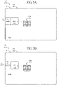
- FIG. 1 describing prior art, illustrates a smart card SC 100 in cross-section, along with a contact reader and a contactless reader.
- An antenna module AM (or transponder chip module TCM) 110 may comprise a module tape (MT) 112, an RFID chip (CM) 114 disposed on one side (face-down) of the module tape MT along with a module antenna (MA) 116 and contact pads (CP) 118 disposed on the other (face-up) side of the module tape MT for interfacing with an external contact reader.
- the card body (CB) 120 comprises a substrate which may have a recess (R) 122 extending into one side thereof for receiving the antenna module AM
- the recess R may be stepped - such as wider at the surface of the card body CB - to accommodate the profile of the antenna module AM.
- the booster antenna BA 130 may comprise turns (or traces) of wire (or other conductor) embedded in (or disposed on) the card body CB, and may comprise a number of components such as (i) a card antenna (CA) component 132 and (ii) a coupler coil (CC) component 134. It may be noted that, as a result of the recess R being stepped, a portion of the card body CB may extend under a portion of the antenna module AM, more particularly under the module antenna MA.
- Metal foils, metallic coatings, segments of metal foil or metal particles may be deposited on or embedded in the inlay (or card body CB) to alter the electrical characteristics of the RFID device or smartcard.
- a metal foil layer in the card body construction may helps to meet the ISO and EMV communication standards for RFID devices or smart cards in terms of read write distance, baud rate, Q-factor bandwidth, etc.
- the metal foil can be any pure metal such as aluminum or copper or an alloy.
- the metal foils, metallic coatings, segments of metal foil or metal particles should have a thickness less than the skin depth of the metal or material being used in order to prevent the formation of eddy currents in the metal or metallic structure that will attenuate the RF electromagnetic field.
- thicknesses substantially less than the skin depth of the metal or material being used will increase the electrical resistance of the structure to alternating current flows (impedance) thereby preventing unwanted or excessive attenuation of the RF electromagnetic field.
- Other electrical conductors such as metal nanoparticles, metal nanowires or carbon-based conductors like graphite or exfoliated graphite can be used to construct electrically conductive networks that are hereby included under the definition of a metal foil or metallic structure.
- Holographic metal foils may be glued or laminated to both sides of the booster antenna BA inlay (card body CB).
- the holographic metal foils may not significantly attenuate the electromagnetic field, in other words the holographic metal foils may be largely transparent to the RF field.
- the holographic metal foils can be used to mask (visually hide) the presence of the booster antenna BA.
- the holographic metal foils when placed either side (above, below) of the booster antenna BA can generate capacitance which may help improve the communication performance of the smart card with the reader ( FIG. 1 ).
- holographic metal foils may be glued or laminated to a card body with a booster antenna BA inlay (card body CB) or an inlay with a antenna connected to an RFID chip.
- the holographic metal foils may not significantly attenuate the electromagnetic field, in other words the holographic metal foils may be largely transparent to the RF field if their metal layer thickness may be approximately 30nm.
- the holographic metal foils can be used to mask (visually hide) the presence of a booster antenna BA in a card body.
- holographic metal foils when placed either side (above, below) of a booster antenna BA in a card body may generate capacitance which may help improve the communication performance of the smartcard with the reader.
- Metal foils may comprise a conductive material (such as aluminum on PVC), having a sheet resistance which is very low, on the order of only a few Ohms, which normally should block the electromagnetic field (such as between the booster antenna BA and an external reader, or between the booster antenna BA and the antenna module AM), but a mitigating factor may be the thickness of the aluminum (or other material), being thin enough to allow the electromagnetic field to pass through.
- a conductive material such as aluminum on PVC
- a mitigating factor may be the thickness of the aluminum (or other material), being thin enough to allow the electromagnetic field to pass through.
- Metal foils from CFC (www.cfcintl.com) and Crown (www.crownrollleaf.com) are transparent to high frequency electromagnetic waves because the thickness of the metal layer, approximately 30 nm, is significantly lower the skin depth of the metal at 13.56 MHz.
- the smartcards may comprise a card body (CB).
- the card body may comprise one or more layers having metal foil.
- the smartcards may comprise a transponder chip module (TCM), without a booster antenna.
- the transponder chip module may comprise a dual interface (contact and contactless) chip.
- the transponder chip module may comprise an antenna which is laser-etched from a metal layer (foil or cladding).
- the card body may be milled to have a window opening (W) to accept the transponder chip module.
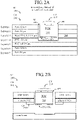
- FIG. 2A is a cross-section of an exemplary stack-up of a metal foil smartcard (SC) 200 and describes prior art.
- the card body (CB) 202 may comprise some of the following layers ...
- the window opening (W) 206 in the card body (CB) is at least as large as the transponder chip module (TCM) 210, to accept installation of the transponder chip module (TCM).
- the window opening (W) may be referred to as a module opening (MO).
- the transponder chip module (TCM) may include an antenna structure (AS) 212 which is laser-etched from a conductive layer (foil or cladding), such as double-sided epoxy glass tape.
- the antenna may be substantially coplanar with the metal film in Layer 3.
- Contact pads (CP) 214 are disposed on the top (as viewed) surface of the transponder chip module (TCM).
- the window opening (W) may be any shape.
- the stack height, not laminated, may be approximately 840 ⁇ m.
- the stack height, laminated may be approximately 800 ⁇ m.
- the metal thickness (in Layer 3) may be approximately 30 nm.
- the antenna may be substantially coplanar with the metal in Layer 3.
- the read/write distance, with a laser etched antenna structure (LES) in the transponder chip module (TCM) and without a booster antenna (BA) in the card body (CB) may be approximately 1.5 cm.
- the performance of a transponder chip module (TCM) in terms of activation distance with an arrangement of contact pads, connection bridges or isolated metal features on its face-up side and a laser-etched antenna structure (LES) connected to an RFID chip (CM) on its face-down side may not be adversely influenced (affected) by the presence of a holographic metal foil in a card body.
- the holographic metal foil laminated to the card body may surround the transponder chip module on all sides and may not adversely influence (affect) its RF performance.
- the thickness of the metal on the foil is a relevant factor.
- Metal foils such as in FIG. 2A are typically thin, and may be too thin and may be so thin (below a transparency threshold) that electromagnetic waves pass through the metallized layer without absorption.
- a metal layer (ML) for a coupling frame (CF), such as in FIG. 2B should be thick enough to conduct electricity and absorb an electromagnetic wave at a frequency of interest and enhance coupling between the transponder chip module (TCM) and an external reader (such as in FIG. 1 ).
- the coupling frame (CF) may be closely adjacent to, but not completely encircle (substantially surround), the transponder chip module (TCM), and may extend from adjacent the transponder chip module (TCM) to one or more outer edges of the metal layer(ML), which may be substantially coincident with the outer edges of the card body (CB).
- the transponder chip module may have a laser-etched (versus chemically etched, or versus wire-wound) antenna structure (LES) serving as a planar antenna structure with feature sizes (such as spaces between tracks) of approximately 25 ⁇ m, which may be achieved by laser etching. (Chemical etching may be limited to feature sizes on the order of 100 ⁇ m).
- LES laser-etched antenna structure
- US 14281876 filed 19 May 2014 discloses LASER ABLATING STRUCTURES FOR ANTENNA MODULES FOR DUAL INTERFACE SMARTCARDS.
- Laser etching antenna structures for RFID antenna modules (AM) and combining laser etching and chemical etching are disclosed. Limiting the thickness of the contact pads (CP) to less than the skin depth (18 ⁇ m) of the conductive material (copper) used for the contact pads (CP).
- Multiple antenna structures (AS1, AS2) in an antenna module (AM), and incorporating LEDs into the antenna module (AM) or smartcard (SC) are also disclosed.
- the antenna may be laser etched from a copper layer (cladding or foil), which may have a thickness less than the skin depth of copper ( ⁇ 18 ⁇ m), forming a number of tracks separated by a distance approximately equal to the width of the laser beam, such as approximately 25 ⁇ m. Subsequent to laser etching, the antenna structure may be plated, which may reduce the distance between tracks to approximately 20 ⁇ m (for example). This may result in increased performance of the antenna structure, and the overall antenna module AM (or transponder chip module (TCM)), and reduce performance constraints on the performance of a booster antenna (BA) in the card body (CB) of the smartcard (SC).
- a booster antenna BA
- a metal surface or a conductive surface of suitable thickness and dimension acting as a coupling frame (CF) obviates the need for a booster antenna (BA) in a dual interface smartcard (SC).
- the coupling frame in a card body (CB), tag, document or the like may act as a capacitive coupling antenna, concentrating the electromagnetic field around the transponder chip module (TCM) which may have a laser-etched antenna structure (LES).
- TCM transponder chip module
- LES laser-etched antenna structure
- LES laser-etched antenna structure
- TCM transponder chip module
- AS antenna structure
- MF metal frame
- CF coupling frame
- a dual interface smart card comprises:
- FIG. 2B shows, generally, a smart card (SC) 200 having a card body (CB) 202.
- the card body (CB) may comprise several layers laminated together.
- a coupling frame (CF) 220 is shown disposed in (or on) a given layer ("a layer") so as to be adjacent to, or surround the transponder chip module (TCM).
- the transponder chip module (TCM) 210 may comprise a laser-etched antenna structure (LES) 212.
- LES laser-etched antenna structure
- the antenna structure (AS) may be formed by laser etching, having a number of (such as 10 or 12) tracks which are disposed substantially planar with one another on a module tape (MT) or other suitable substrate, in a generally rectangular spiral pattern.
- the spacing between tracks may be on the order of 25 ⁇ m, or less (such as 20 ⁇ m, after plating).
- the metal frame (or layer), forming an open loop coupling frame (CF) may be substantially coplanar with the antenna structure (AS), and may be disposed adjacent at least one, at least two or at least three sides of the transponder chip module (TCM).
- the coupling frame (CF) may nearly encircle the transponder chip module (TCM), is formed as an open loop and has two ends, or as a loop having at least two segments (and corresponding at least four ends).
- the metal frame (MF) may comprise a copper foil or cladding, may be laminated to a layer of the card body (CB) of the smart card (SC), and may have a thickness of approximately 12, 18 or 35 ⁇ m.
- the coupling frame (CF) may tend to concentrate the electromagnetic flux, acting (by way of analogy) as a coupler coil (CC, 134).
- more than one coupling frame, or portions (CF1, CF2 ... CFn) of an overall coupling frame (CF) may be disposed concentrically around the transponder chip module (TCM).
- the coupling frame may be referred to as a metal frame (MF), and vice-versa.
- a metal layer ML
- MB metal card body
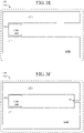
- FIG. 2C shows an example of a smartcard (SC) 200 with a coupling frame (CF) 220 incorporated into its card body (CB) 202 which has a stepped recess (R).
- a transponder chip module (TCM) 210 has a laser-etched antenna structure (LES) 212, an outer portion of which overhangs an inner portion of the coupling frame (CF).
- the coupling frame (CF) has an opening (MO) 208 for receiving the transponder chip module (TCM) 210.
- the dashed line indicates, schematically, either a metal layer in a stackup of a card body, or a substantially entirely metal card body (CB). When “metal layer” is referred to herein, it may refer to such a metal card body.
- FIG. 2D shows a transponder chip module (TCM) 210 disposed in the card body (CB) 202m of a metal smartcard (SC) 200m, or metal card (MC), wherein substantially the entire card body (e.g., 760 ⁇ m thick) comprises metal, and may be referred to as a metal card body (MCB).
- MC metal card body
- TCM transponder chip module
- the transponder chip module (TCM) resides in an opening (MO) 208, in the metal card body (MCB) 202 which may also be referred to as a module opening (MO).
- the opening (MO) may be prepared by mechanical milling, or laser ablation, and may be at least the size of the laser etched antenna structure (LES) 212, and may be stepped (for an example of a stepped recess/opening, see FIG. 2C ) so that a portion of the metal card body (MCB) overlaps (underneath, as viewed) an outer portion of the laser-etched antenna structure (LES).
- LES laser etched antenna structure
- antenna structures which are other than laser-etched may be substituted for the laser-etched antenna structure (LES), if they can be made to exhibit sufficient performance, such as by having appropriate track width and spacing between tracks.
- the back (bottom, as viewed) of the metal card body (MCB) should be open (free of metal, non-conductive) to avoid attenuation of the electromagnetic field.
- the opening (CO, or MO) should extend completely through the card body.
- TCM transponder chip module
- the void can be filled with a resin or with an active synthetic material ("filler") which illuminates during an electronic transaction (e.g., whilst being interrogated by an external reader).
- the void beneath the transponder chip module (TCM) could be a series of perforations, a slit or annulus that permits communication of the transponder chip module with the reader.
- a slit (or slot, or gap, or band) (S) 230 is provided through the metal card body (MCB) so that it can function as a coupling frame (CF) for capacitive coupling with a contactless reader.
- a card body (CB) with a coupling frame (CF), or a metal card body (MCB) modified (such as with a slit) to act as a coupling frame (CF) may be provided as an interim product, into which a transponder chip module (TCM) may later be installed.
- a substantial improvement in the activation distance of the Transponder IC Module may be achieved by placing a coupling frame (isolated conductor) around the transponder chip module (TCM), so long as the frame does not fully surround the module.
- a coupling frame isolated conductor
- tungsten plates were disposed around 3 sides of the module, which increased the activation distance from 18 mm to approximately 40 mm.
- the tungsten plates extended past the card body area.
- the coupling frame (CF) should be designed to fit within a standard card body area (54 mm ⁇ 86 mm).
- activation distance and “read/write distance” may be used interchangeably, an increase in one tending to manifest itself in a corresponding increase in the other.
- This phenomenon has also been shown to work with 35 ⁇ m thick electrodeposited copper sheets, aluminum (aluminium), stainless steel, tungsten and ferrite material (magnetic particles) and is likely to work with any metal with a high enough conductivity.
- TCM transponder chip module
- a module size similar in dimensions to an 8 contact module, transponder chip module (TCM) with a laser-etched antenna structure (LES) was used, with dimensions of: 12.6 mm ⁇ 11.4 mm. 35 ⁇ m electrodeposited copper was used as the material for the coupling frame (CF).
- the coupling frame (CF) was disposed closely adjacent to the perimeter of the transponder chip module (TCM).
- An RFID reader operating at 13.56 MHz was used to measure the activation distance.
- the "baseline" activation distance for the transponder chip module (TCM) itself was determined to be approximately 18 mm.
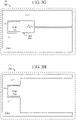
- FIG. 3A shows a coupling frame (CF) 320A disposed on one side of a transponder chip module (TCM) 310 in a card body (CB) 302.
- the coupling frame (CF) is disposed on only one side (lower, as viewed) of the transponder chip module (TCM), and extends from the lower (as viewed) edge of the transponder chip module (TCM) towards the lower edge of the card body (CB).
- the coupling frame (CF) also extends towards the left (as viewed) edge of the card body (CB).
- the coupling frame (CF) is larger (in area) than the transponder chip module (TCM), and may cover about 15% of the overall card area. (The percentages set forth herein are approximate.) An activation distance of 21 mm was achieved.
- FIG. 3B shows a coupling frame (CF) 320B disposed on two (opposite) sides of a transponder chip module (TCM) 310 in a card body (CB) 302.
- the coupling frame (CF) comprises two separate portions - a first portion (CF1) disposed below the transponder chip module (TCM), similar to the previous embodiment ( FIG. 3A ), and a second portion (CF2) disposed above the transponder chip module (TCM).
- the two portions (CF1, CF2) of the overall coupling frame (CF) are not connected with one another, and surround two opposite sides of the transponder chip module (TCM) and, in aggregate cover about 25% of the overall card area. An activation distance of 25 mm was achieved.
- FIG. 3C shows a coupling frame (CF) 320C disposed on two (adjacent) sides of a transponder chip module (TCM) 310 in a card body (CB) 302.
- the coupling frame (CF) comprises a first portion (CF1) disposed below the transponder chip module (TCM), similar to the previous embodiment ( FIG. 3B ), and a second portion disposed to the left (as viewed) of the transponder chip module (TCM).
- the two portions are contiguous with one another, and surround two adjacent sides of the transponder chip module (TCM). An activation distance of 24 mm was achieved.
- the transponder chip module is rectangular, having four sides. If the transponder chip module (TCM) were circular or elliptical, for example, rather than a coupling frame (CF) being disposed closely adjacent to and surrounding two or three or four "sides" of the transponder chip module (TCM), the coverage of the coupling frame (CF), vis-à-vis the transponder chip module (TCM) may be expressed in degrees, from 0° to 360° - for example,
- FIG. 3D shows a coupling frame (CF) 320D disposed on three sides (bottom, top, left) of a transponder chip module (TCM) 310 in a card body (CB) 302.
- the coupling frame (CF) comprises a first portion (CF1) disposed below the transponder chip module (TCM), a second portion (CF2) disposed to the left (as viewed) of the TCM, and a third portion (CF3) disposed above (as viewed) the transponder chip module (TCM).
- the three portions (CF1, CF2, CF3) are contiguous with one another, and surround three sides (or 270°) of the transponder chip module (TCM).
- the third portion (CF3) is shown extending nearly to the top edge of the card body (CB).
- the second portion (CF2) is shown extending nearly to the left edge of the card body (CB).
- the first portion (CF1) is shown extending towards, bur not nearly to, the bottom edge of the card body (CB).
- the interior edges of the three portions (CF1, CF2, CF3) are disposed closely adjacent the outer edges of the transponder chip module (TCM), and the antenna structure (AS) or laser-etched antenna structure (LES) in the transponder chip module (TCM). An activation distance of 28 mm was achieved.
- FIG. 3E shows a coupling frame (CF) 320E disposed on three sides (bottom, top, left) of a transponder chip module (TCM) 310 in a card body (CB) 302.
- the coupling frame comprises a first portion (CF1) disposed below the transponder chip module (TCM), a second portion (CF2) disposed to the left (as viewed) of the transponder chip module (TCM), and a third portion (CF3) disposed above (as viewed) the transponder chip module (TCM).
- the three portions (CF1, CF2, CF3) are contiguous with one another, and surround three sides (or 270°) of the transponder chip module (TCM).
- the first and third portions extend substantially to the lower and upper (as viewed) edges of the card body (CB).
- the second portion (CF2) extends substantially to the left (as viewed) edge of the card body (CB).
- the first and third portions also extend substantially to the right (as viewed) edge of the card.
- This coupling frame (CF) surrounds three sides (or 270°) of the transponder chip module (TCM), and may cover a substantial portion (such as more than approximately 80%) of the card. An activation distance of 30 mm was achieved.
- FIG. 3F shows a coupling frame (CF) 320F disposed on three sides (bottom, top, left) of a transponder chip module (TCM) 310 in a card body (CB) 302.
- the coupling frame (CF) comprises a first portion (CF1)disposed below the transponder chip module (TCM), a second portion (CF2) disposed to the left (as viewed) of the transponder chip module (TCM), and a third portion (CF3) disposed above (as viewed) the transponder chip module (TCM).
- the three portions are contiguous with one another, and surround three sides (or 270°) of the transponder chip module (TCM).
- the first and third portions extend substantially to the lower and upper (as viewed) edges of the card.
- the second portion (CF2) extends substantially to the left (as viewed) edge of the card body (CB).
- the first and third portions also extend substantially to the right (as viewed) edge of the card body (CB).
- An end (right, as viewed) of the first portion (CF1) extends upward near the right edge of the card body (CB), and an end (right, as viewed) of the third portion (CF3) extends downward near the right edge of the card body (CB).
- This coupling frame (CF) surrounds three sides of the transponder chip module (TCM), and may cover a substantial portion (such as more than approximately 82%) of the card body (CB). An activation distance of 32 mm was achieved.
- FIG. 3G shows a coupling frame (CF) 320G disposed on three sides (bottom, top, left) of a transponder chip module (TCM) 310 in a card body (CB) 302.
- the coupling frame (CF) comprises a first portion (CF1) disposed below the transponder chip module (TCM), a second portion (CF2) disposed to the left (as viewed) of the transponder chip module (TCM), and a third portion (CF3) disposed above (as viewed) the transponder chip module (TCM).
- the three portions (CF1, CF2, CF3) are contiguous with one another, and surround three sides (or 270°) of the transponder chip module (TCM).
- the first and third portions extend substantially to the lower and upper (as viewed) edges of the card body (CB).
- the second portion extends substantially to the left (as viewed) edge of the card body (CB).
- the first and third portions also extend substantially to the right (as viewed) edge of the card.
- An end portion (right, as viewed) of the first portion (CF1) extends upward from near the right edge of the card body (CB) to about halfway across the card body (CB), and an end portion (right, as viewed) of the third portion (CF3) extends downward from near the right edge of the card body (CB) to about halfway across the card body (CB).
- the coupling frame (CF) has an opening (MO) 308 for receiving the transponder chip module (TCM), surrounds three sides (or 270°) of the transponder chip module (TCM), and may cover a substantial portion (such as more than approximately 85%) of the card body (CB). An activation distance of 34 mm was achieved.
- FIG. 3H shows a coupling frame (CF) 320H disposed on three sides (bottom, top, left) of a transponder chip module (TCM) 310 in a card body (CB) 302.
- the coupling frame (CF) comprises a first portion (CF1) disposed below the transponder chip module (TCM), a second portion (CF2) disposed to the left (as viewed) of the transponder chip module (TCM), and a third portion (CF3) disposed above (as viewed) the transponder chip module (TCM).
- the three portions (CF1, CF2, CF3) are contiguous with one another, and surround three sides (or 270°) of the transponder chip module (TCM).
- the first and third portions extend substantially to the lower and upper (as viewed) edges of the card body (CB).
- the second portion extends substantially to the left (as viewed) edge of the card body (CB).
- the first and third portions also extend to the right (as viewed) edge of the card body (CB), but this extension of the first and third portions is narrower than that shown in FIG. 3G .
- This coupling frame (CF) surrounds three sides (or 270°) of the transponder chip module (TCM), and may cover a portion (such as approximately 30%) of the card body (CB). An activation distance of 28 mm was achieved.
- the actual spacing (or separation, or gap) of interest may be the distance between the inside edge of the coupling frame (CF) and the outer track of the laser-etched antenna structure (LES) of the transponder chip module (TCM) which extends nearly to the outer edge(s) of the overall transponder chip module (TCM).
- the gap may be reduced almost to zero and, with a stepped recess in the card body (CB), the coupling frame (CF) may actually slightly overlap outer tracks of the laser-etched antenna structure (LES) separated by an adhesive layer (approximately 30 ⁇ m) which acts as a dielectric medium. See FIG. 2C .
- CF coupling frame
- Extending the coupling frame (CF) entirely (rather than partially) across the width of the card body (CB), without openings in the metal layer (ML) forming the coupling frame (CF), may significantly improve (increase) activation distance, which may indicate that an enlarged metallic area around the transponder chip module (TCM) provided by the coupling frame (CF) improves the capacitive coupling with the reader.
- TCM transponder chip module
- Separation of (or, gap between) the coupling frame (CF) from (and) the transponder chip module (TCM) may have a significant impact, with reduced separation (smaller gap) resulting in increased activation distance.
- the thickness of the coupling frame (CF) does not appear to have any impact on the coupling frame's performance.
- Conductive materials other than copper may be used as a material for the conducting frame (CF).
- the activation distance of an 8-contact (8 contact pads) transponder chip module (TCM) used in trials was 18 mm without the coupling frame (CF). With the coupling frame (CF), the activation distance was increased by approximately 10 mm, or more than 50%, to approximately 28 mm.
- the coupling frame (CF) may extend into the embossing area (lower half) of the card body (CB), and when sized back to avoid the embossing area, there may be a negatively effect on the performance of the coupling frame (CF). However this may be overcome by reshaping the coupling frame (CF), or rotating it, so that the coupling frame (CF) no longer encroaches upon the embossing area.
- CF card body
- TCM transponder chip module
- LES laser-etched antenna structure
- Coupling frames can be made from foil metals, thickness from 9 - 100 ⁇ m or from bulk metal with thickness up to the total normal thickness of a smartcard (760 ⁇ m).
- the metal can be any metal or alloy, for example copper, aluminum, brass, steel, tungsten, titanium.
- the metal foil may be of any origin, e.g. electrodeposited or roll annealed.
- the coupling frames (CF) may be made by electroless deposition on a substrate followed by electroplating.
- the coupling frame can be formed from a metal insert or slug placed in the card body (CB) to increase weight of the card.
- the metal insert may acts as a coupling frame when used with an appropriate laser etched antenna structure (LES).
- the coupling frame (CF) can be formed from a conductive material deposited on a substrate.
- a conductive material deposited on a substrate.
- conductive carbon paste silk screen printed onto paper or silver particulate ink silk screen printed onto PET with subsequent annealing to allow formation of a conductive film.
- the coupling frame (CF) can be formed from vapor deposited or sputter coated metals (e.g. aluminum) on plastic coated substrates.
- the coupling frame may be formed from a loop of wire.
- the loop of wire may be embedded in a plastic substrate.
- the coupling frame may overlap part of the laser etched antenna structure (LES) in order to increase the electromagnetic coupling between these components and hence increase the performance of the smartcard.
- LES laser etched antenna structure
- overlap of the coupling frame CF over the antenna of the transponder chip module (TCM) may result from or may require that there is a stepped recess in the card body CB) for receiving the transponder chip module TCM).
- the laser-etched antenna structure (LES) on the transponder chip module may be co-planar with the coupling fame (CF), with a gap therebetween of 50 - 300 ⁇ m.
- the laser-etched antenna structure (LES) could also be overlapping the coupling frame in a stepped recess. If the coupling frame (CF) is overlapping the laser-etched antenna structure (LES), the distance (vertical offset) between the tracks of the laser-etched antenna structure (LES) tracks and the coupling frame (CF) should have a minimum distance of approximately 30 ⁇ m, with a dielectric material therebetween such as adhesive tape (Tesa) or resin holding or fixing the antenna module (AM) or transponder chip module (TCM) in place.
- adhesive tape Tesa
- AM antenna module
- TCM transponder chip module
- the coupling frame (CF) may host (be provided with, may comprise) an engraving, embossing, or stamped feature/logo/ID which serves as a security feature for the smartcard.
- This feature may or may not be visible on the card surface after lamination of the card stack-up. This feature may be visible on X-ray, CT or other scanning equipment such as that used at security screening points (e.g. in airports). This feature may permit identification of the card and be used to validate the authenticity of a given card.
- TCM transponder chip module
- CF coupling frame
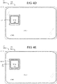
- FIG. 4A illustrates an embodiment of a smartcard 400A having a multiple coupling frame stack-up.
- the stack-up comprises a front face card layer 424, a first coupling frame (CF-1) 421, an internal card dielectric layer 423, a second coupling frame (CF-2) 422 and a rear face card layer 426.
- the first coupling frame (CF-1) surrounds the top, left and bottom edges of the transponder chip module (TCM) 410, and extends to the top, left and bottom edges of the card body (CB), and has a module opening (MO-1).
- the second coupling frame (CF-2) surrounds the top, right and bottom edges transponder chip module (TCM), and extends to the top, right and bottom edges of the card, and has a module opening (MO-2).
- the first and second coupling frames (which may be referred to as "420”) cover nearly the entire surface of the card body 402 (less the area of the transponder chip module TCM). An activation distance of 40 mm was achieved.
- FIG. 4B illustrates an embodiment of a smartcard 400B having a coupling frame (CF) 420B in the form of a ring having a circular outer periphery and a rectangular module opening (MO) in the metal layer (ML) of the coupling frame (CF) whereat the transponder chip module (TCM) 410 may be disposed.
- the coupling frame (CF) nearly completely surrounds the transponder chip module (TCM), except for a slit (S) 430.
- the slit (S) is shown on the right side of the transponder chip module (TCM), but could extend from any side thereof (more accurately, from any position in the module opening (MO 408).
- the slit (S), or gap between the opposed ends of the coupling frame (CF), is important so that the coupling frame (CF) is not a closed loop, but rather is an open loop.
- the slit (S) extends from the module opening (MO) to the periphery (outer edge) of the coupling frame (CF), and may be very narrow (small width).
- the coupling frame (CF) in this example is a few times larger than the transponder chip module (TCM), and may cover approximately 15% of the card body (CB) 402. An activation distance of 33 mm was achieved.
- the slit (S) may be much smaller than the module opening (MO).
- the module opening (MO) is approximately 10 x 10 mm, depending on the size of the transponder chip module (TCM).
- the 50 ⁇ m size (width) for the slit (S) is approximate, and exemplary.
- a 50 ⁇ m wide slit (S) would be approximately 0.5% of the size of the module opening (MO).
- the slit may be less than 50% of the size of the module opening (MO), including less than 25%, less than 10%, less than 5% and less than 1% of the size of the module opening (MO).
- the slit (S) may be filled with a non-conductive material.
- the coupling frame (CF) would be adjacent three sides of the transponder chip module (TCM), as in FIG. 3D , for example.
- the slit (S) may be formed by laser etching, which is suitable for forming a very narrow (e.g., 50 ⁇ m) slit in some materials. Other materials are not amenable to laser etching, and may require conventional mechanical processes to form a wider slit, or slot.
- the slit (S) may extend in any direction, from anywhere on the module opening (MO) to the periphery of the metal layer (ML) of the coupling frame (CF), so that the coupling frame (CF) is an open loop, having two ends (or end portions). And, the slit (S) may extend only partially through the metal layer (ML) of the coupling frame (CF), leaving only a very thin layer of metal which is transparent to electromagnetic waves below the slit.
- FIG. 4C illustrates an embodiment of a smartcard 400C having a coupling frame (CF) 420C in the form of a ring having an elliptical outer periphery and a rectangular module opening (MO) whereat the transponder chip module (TCM) 410 may be disposed.
- the coupling frame (CF) nearly completely surrounds the transponder chip module (TCM), except for a slit (S) 430.
- the slit (S) is shown on the left side of the transponder chip module (TCM), but could extend from any side thereof (more accurately, from any position in the module opening (MO 408).
- the slit (S) extends from the module opening (MO) to the outer periphery of the coupling frame (CF), and may be very narrow (small width).
- the coupling frame (CF) in this example is a few times larger than the transponder chip module (TCM), and may cover approximately 20% of the card body (CB) 402. An activation distance of 35 mm was achieved.
- FIG. 4D illustrates a not-claimed example of a smartcard 400D having a coupling frame (CF) 420D comprising a first, inner ring-shaped coupling frame (CF-1) disposed around and completely surrounding the transponder chip module (TCM) 410 and an outer coupling frame (CF-2) disposed around and spaced outward from the inner coupling frame (CF-1) and extending substantially to the periphery of the card body (CB) 402.
- both of the coupling frames (CF-1, CF-2) are closed loops.
- This figure shows a first closed loop (no slit) coupling frame disposed around the transponder chip module (TCM), and a second closed loop (no slit) coupling frame (CF-2) disposed substantially concentrically around the first coupling frame (CF-1).
- the first coupling frame (CF-1) is only slightly larger than the transponder chip module (TCM).
- the second coupling frame (CF-2) may extend to the top, bottom, left and right edges of the card, covering nearly 100% of the card area (less the module opening MO and the first coupling frame CF-1).
- This configuration wherein the coupling frame(s) (CF-1, CF-2) are closed loop (no slits), may not improved activation distance and, in fact, may impair it.
- FIG. 4E illustrates an embodiment of a smartcard 400E having a coupling frame (CF) 420E comprising an inner ring-shaped coupling frame (CF-1) disposed around and completely surrounding the transponder chip module (TCM) 410 and an outer coupling frame (CF-2) disposed around and spaced outward from the inner coupling frame (CF-1) and extending substantially to the periphery of the card body (CB) 402.
- This figure shows a first open loop (with a slit S, 430) coupling frame (CF-1) disposed around the transponder chip module (TCM), and a second closed loop (no slit) coupling frame (CF-2) disposed substantially concentrically around the first coupling frame (CF-1).
- the first coupling frame (CF-1) is only slightly larger than the transponder chip module (TCM).
- the second coupling frame (CF-2) may extend to the top, bottom, left and right edges of the card, covering nearly 100% of the card area (less the module opening MO and the first coupling frame CF-1).
- This configuration wherein the first coupling frame (CF-1) is open loop (has a slit (S)), and the second coupling frame (CF-2) is closed loop (no slit), may not significantly improve activation distance.
- FIG. 4F illustrates an embodiment of a smartcard 400F having a coupling frame (CF) 420F comprising an inner ring-shaped (CF-1) disposed around and completely surrounding the transponder chip module (TCM) 410 and having a slit (S) 430, and an outer coupling frame (CF-2) disposed around and spaced outward from the inner coupling frame (CF-1) and also have a slit and extending substantially to the periphery of the card body (CB) 402.
- both of the coupling frames (CF-1, CF-2) are open loops.
- This figure shows a first open loop (with a slit) coupling frame (CF-1) disposed around the transponder chip module (TCM), and a second open loop (with a slit) coupling frame (CF-2) disposed substantially concentrically around the first coupling frame (CF-1).
- the first coupling frame (CF-1) is only slightly larger than the transponder chip module (TCM).
- the second coupling frame (CF-2) may extend to the top, bottom, left and right edges of the card body (CB).
- the slits (S) in the first and second coupling frames are shown as both being disposed to the left of the transponder chip module (TCM). An activation distance of 36 mm was achieved.
- FIG. 4G illustrates embodiment of a smartcard 400G having multiple linked open loop coupling frames, with full card size outer frame, in a card body (CB) 402.
- the overall coupling frame (CF) 420G may be characterized as having a number of ring cutouts in it, concentrically, at increasing distances from the transponder chip module (TCM) 410.
- a first portion (CF1) of the coupling frame (CF) is disposed nearly fully around the transponder chip module (TCM), separated therefrom by a gap ("gap").
- a second portion (CF2) of the coupling frame (CF) is disposed around the first portion (CF1) of the coupling frame (CF), separated therefrom by a ring-shaped cutout ("cutout") nearly fully encircling the transponder chip module (TCM).
- a second portion (CF2) of the coupling frame (CF) is disposed nearly fully around the first portion (CF1) of the coupling frame (CF), separated therefrom by a ring-shaped cutout ("cutout").
- the first coupling frame (CF1) is only slightly larger than the transponder chip module (TCM).
- the slits (S) 430 in the first and second portions (CF1, CF2) of the coupling frame (CF) are shown as all being disposed to the left of the transponder chip module (TCM).
- the ends of the coupling frame portions (CF1, CF2) are connected with one another. (It may be noted that, without the cutouts, thereby being one large coupling frame with a slit, this configuration would resemble the embodiment shown in FIG. 5G.) An activation distance of 38 mm was achieved.
- FIG. 4H shows a smartcard 400H having a coupling frame (CF) 420H made of tungsten or other high density metal or metal alloy, and surrounding only two adjacent sides (or 180°) of a transponder chip module (TCM) 410.
- the coupling frame (CF) extends from the right (as viewed) edge of the transponder chip module TCM) to the right (as viewed) edge of the card body (CB) 402, and from the bottom (as viewed) edge of the transponder chip module TCM) to the bottom (as viewed) edge of the card body (CB).
- the coupling frame (CF) may comprise tungsten or other high density metal or metal alloy. An activation distance of 25 mm was achieved.
- FIG. 4H bears some resemblance to FIG. 1 of US 61978187 , which shows a DIF smartcard body with a metal slug and booster antenna.
- BA booster antenna
- FIG. 4I shows an embodiment of smartcard 4001 having a coupling frame (CF) 4201 made of tungsten or other high density metal or metal alloy, and surrounding all four sides (nearly 360°) of a transponder chip module (TCM) 410.
- a coupling frame (CF) surrounds the transponder chip module TCM), and has a slit (S) 430 on its left (as viewed) side.
- the coupling frame (CF) extends from the right (as viewed) edge of the transponder chip module TCM) nearly to the right (as viewed) edge of the card body (CB) 402, from the bottom (as viewed) edge of the transponder chip module TCM) towards the bottom (as viewed) edge of the card body (CB), and from the top (as viewed) edge of the transponder chip module TCM) towards the top (as viewed) edge of the card body (CB), and may cover approximately 60% of the area of the card body (CB).
- the coupling frame (CF) may comprise tungsten or other high density metal or metal alloy.
- the coupling frame (CF) has an opening (MO) for the transponder chip module (TCM). A gap between the coupling frame (CF) and the transponder chip module (TCM) should be maintained as small as possible. An activation distance of 35 mm was achieved.
- FIG. 5A shows a metal layer (ML) which may be a card body 502 of a metal-faced smartcard 500A (or card body 502 of a metal card) modified to function as an open-loop coupling frame (CF) 520A, showing a coupling frame (CF) surrounding three sides (or 270°) of the transponder chip module (TCM) 510.
- the left side of the transponder chip module (TCM) is not surrounded. Rather, a non-conductive filler (“filler") material may bridge the large slit (S, or slot, or band) between the ends of the coupling frame (CF) to the left (as viewed) of the transponder chip module (TCM).
- a coupling frame surrounds three sides (top, bottom and right) of the transponder chip module (TCM) disposed in a module opening (MO) 508.
- the coupling frame (CF) extends from the right (as viewed) edge of the transponder chip module (TCM) to the right (as viewed) edge of the card body (CB), from the bottom (as viewed) edge of the transponder chip module (TCM) to the bottom (as viewed) edge of the card body (CB), and from the top (as viewed) edge of the transponder chip module (TCM) to the top (as viewed) edge of the card body (CB).
- the "slit" (S) 530 is large, extending nearly the height (approximately 10mm) of the transponder chip module (TCM), and may be referred to as a "slot" or "band".
- the coupling frame (CF) may comprise tungsten or other high density metal or metal alloy, and may constitute substantially the entire card body (CB).
- the filler material may have a thickness corresponding to the thickness of the coupling frame (CF), and may comprise a material that may illuminate when the smartcard (SC) is being interrogated by an external reader.
- FIG. 5B shows a metal layer (ML) which is a card body 502 of a metal-faced smartcard 500B (or card body of a metal card) modified to function as an open-loop coupling frame (CF) 520B, showing a coupling frame (CF) surrounding four sides (or nearly 360°) of the transponder chip module (TCM) 510 disposed in a module opening (MO) 508.
- a slit (S) 530 is disposed through the coupling frame on the left (as viewed) side of the transponder chip module (TCM), and may be filled with a non-conductive filler material ("filler").
- a coupling frame surrounds all four sides (top, bottom, right and left) of the transponder chip module (TCM).
- the coupling frame (CF) extends from the right (as viewed) edge of the transponder chip module (TCM) to the right (as viewed) edge of the card body (CB), from the bottom (as viewed) edge of the transponder chip module (TCM) to the bottom (as viewed) edge of the card body (CB), and from the top (as viewed) edge of the transponder chip module (TCM) to the top (as viewed) edge of the card body (CB).
- the portion of the coupling frame (CF) on the left of the transponder chip module (TCM) has a slit, rather than a band (in either case, slit or band, the coupling frame is open loop).
- the coupling frame (CF) may comprise tungsten or other high density metal or metal alloy and may constitute substantially the entire card body (CB).
- the filler material may have a thickness corresponding to the thickness of the coupling frame (CF), and may comprise a material that may illuminate when the smartcard (SC) is being interrogated by an external reader.
- a metal card made of steel may exhibit an activation distance of approximately 40 mm with a barely visible slit width of approximately 50 ⁇ m.
- the slit (S) in the coupling frame (CF) can be laser etched, mechanical removed or chemically etched.
- the thickness of the metal layer (ML) can be from approximately 1 ⁇ m to approximately 35 ⁇ m, or greater, and may be laminated to a synthetic core (PVC, PC, Paper, PETG, Teslin) etc.
- a metal card, or plastic card with a metal slug or metal core may have a metal (layer, body, core or slug) thickness of approximately 300 - 760 ⁇ m.
- Metal foils may be integrated into plastic cards and may be arranged to function as a coupling frame (CF).
- the metal foils have a metal layer thickness of at least 1 micron which is a fraction of the skin depth thickness of the metal or conductive layer at 13.56 MHz (the frequency of interest is in the range 10 - 30 MHz).
- Metal foils with a skin depth thickness of 12 micron have been tested, which have performed in the same manner as a metal substrate with a thickness equal to 0.76 mm (card body thickness).
- Metal foils such as holographic metal foils with a thickness of 30 nm may be integrated into plastic cards. These foils may not be appropriate for a coupling frame (CF), but they may add to the aesthetics of the card, without interfering with the electromagnetic field.
- CF coupling frame
- the coupling frames (CF) described herein may surround the transponder chip module on all four sides (less the slit S), on three sides or on two sides. It is important that the metal or conductive frame (CF) is an open loop, forming an open circuit around the transponder chip module (TCM). This is achieved by creating a slit which emanates from one or more sides of the module opening (MO) for the transponder chip module (TCM) and extends to the edge of the metal layer (ML) or conductive frame (CF).
- the metal foil (or metal layer ML, or metal core, or metal card body) can be any metal or metal alloy such as copper, aluminium, brass, titanium, tungsten, stainless steel.
- the metal foil may also be substituted with an alternative electrically conducting material or film such as silk screen printed silver ink, vapour deposited metals, graphene, silver nanowires or conductive carbon ink.
- the metal foil may also be substituted by a perforated metal mesh or wireframe metal mesh.
- ML slotted metal layer
- CF coupling frame
- TCM transponder chip module
- LES planar, laser-etched antenna structure
- Chemically etched antenna structures on the face down side of a module tape may have a spacing between tracks of 100 ⁇ m which may not interact (function) as well with a coupling frame (CF) as a laser-etched antenna structure (LES). Consequently, such antenna modules (AM) with a chemical etched antenna may have a very low activation distance with a reader, such as 1 mm, thereby requiring a booster antenna (BA) in the card body (CB).
- BA booster antenna
- the transponder chip module can interact well with the coupling frame (CF), and in some applications may function adequately without a coupling frame (CF) (and, indeed, without a booster antenna (BA)).
- the activation distance for a transponder chip module (TCM) having a laser-etched antenna structure (LES; spacing between tracks of 25 ⁇ m) depending on the position over the reader can range from 15 to 20 mm. If you add the slotted coupling frame, the activation distance increases, with a range from 30 mm to 40 mm.
- the antenna structure (AS) of a transponder chip module (TCM), which may be a laser-etched antenna structure (LES), may comprise a rectangular spiral track having approximately 10-12 turns, the width of each track being approximately 100 ⁇ m, the spacing between tracks being approximately 25 ⁇ m.
- Chemically-etched antenna structures may have larger feature sizes (e.g., spacing of 100 ⁇ m between tracks).
- the spaces between tracks of a laser-etched antenna structure (LES) may be less than 100 ⁇ m, less than 75 ⁇ m, less than 50 ⁇ m, and less than 25 ⁇ m. After plating, the spaces between adjacent tracks of a laser etched antenna module (LES) may be even smaller.
- the distance (gap) from the outer track (outer edge, outer feature) of the antenna structure (AS) and the inner edge (or module opening MO) of the coupling frame (CF) should be less than 300 ⁇ m, and more suitably 50 ⁇ m.
- the coupling frame (CF) overlaps an outer feature of the antenna structure (AS), as shown in FIG. 2C .
- the slit or slot in the coupling frame (CF) may be very narrow for aesthetic reasons, for example, a mere 50 ⁇ m in width. (On average, the diameter of a human hair is 100 ⁇ m.)
- the slotted (with a slit) coupling frame (CF) may be a single foil which covers the entire area of a card body (CB), partially covers an area of a card body (CB), or the coupling frame (CF) may comprise several metal or conductive layers which are overlapping.
- a metal foil layer (metal layer of 30 nm) which is transparent to the electromagnetic field may also be part of the card-body stack-up.
- the slit in the coupling frame (CF) may be formed by laser ablation, and may extend from one edge of the module opening (MO) for the transponder chip module (TCM) to the outer perimeter of the coupling frame (CF) or metal layer (ML). This slit may completely penetrate (extend completely through) the metal layer (ML) of the coupling frame (CF), but may also/alternatively only extend partially through the metal layer (ML) of the coupling frame (CF).
- a thin layer of metal may remain and should be below (less than) the transparency threshold for electromagnetic waves, and less than the skin depth (at the required frequency 13.56 MHz) of the metal used to construct the coupling frame, such that electrical current flows across the slit (or void) are minimized and the performance of the coupling frame (CF) is not impeded.
- the void may be filled from one side with a polymer, epoxy resin or similar material to mechanically reinforce the metal frame and fill the void.
- a transponder chip module having a suitable antenna structure (AS), such as a laser-etched antenna structure (LES) having small spaces between tracks
- AS antenna structure
- LES laser-etched antenna structure
- CF coupling frames
- activation distances of at least 20 mm, including at least 25 mm, at least 30 mm, at least 35 mm, up to 40 mm or more may be achieved, without requiring a booster antenna (BA) in the card body (CB), and even in the case of metal cards (wherein the metal layer ML is provided with a slit so that it can function as a coupling frame CF).
- BA booster antenna
- FIG. 6A illustrates the front side of a smartcard 600 which may be a metal card (compare FIG. 5B ) having a metal layer (ML), which may constitute substantially the entire thickness of the card body (CB) 602.
- the card body (CB) has a module opening (MO) 608 wherein a transponder chip module (TCM) 610 may be disposed, and a slit (S) 630 extending from the module opening (MO) to the perimeter of the metal layer (ML) so that the metal card body (MCB) functions as a coupling frame (CF), in the manner described hereinabove.
- the metal layer (ML) (or card body CB, or metal card body MCB) may comprise titanium.
- FIG. 6B illustrates the back (reverse) side of the smartcard 600 shown in FIG. 6A .
- a recessed area 602 may be provided on the reverse side of the card body (CB) to accommodate a magnetic stripe, and may measure approximately 9 mm ⁇ 84 mm.
- Another recessed area 604 may be provided on the reverse side of the card body (CB) to accommodate a signature panel, and may measure approximately 9 mm ⁇ 56 mm.
- the module opening (MO) is shown in dashed lines, and may measure approximately 11 mm ⁇ 13 mm (for an 8 contact module).
- An additional recessed area 606 may be provided on the reverse side of the card body (CB) to accommodate a switch (SW), such as a slide switch, and may measure 5 mm ⁇ 20 mm.
- the switch (SW) may be used to selectively connect/disconnect the ends of the open loop coupling frame (CF) to one another, so that when the ends are connected, the coupling frame (CF) is a closed loop and does not provide the advantages of an open loop coupling frame (CF) as described above. This allows a user to "switch off" the coupling frame feature and its attendant increase in activation distance, which provides more security (an anti-phishing feature) for the user's card.
- the switch feature can be integrated into a solid metal card body construction or a plastic card /metal foil card body construction.
- the switch may comprise a slide switch, a press button switch or the like which can be used to short-circuit the coupling frame (CF) and dampen the function of the transponder chip module (TCM), thereby providing protection against phishing (unauthorized reading of the smartcard).
- the switch (SW) can also have the function of reinforcing the structure of the card body (CB) around the position of slot or slit, protecting it from damage resulting from bending.
- LED Light Emitting Diode
- FIG. 7A shows that an LED (light emitting diode), or other or semiconductor optical device, may be connected across the ends of the coupling frame (CF) in the manner disclosed in FIG. 2 of US 61971636 . See also FIGs. 5, 5A, 5B of US 14281876 .
- the LED is shown connected across the opposing ends of an exemplary elliptical coupling frame (CF) similar to that shown in FIG. 4C (card body (CB) omitted, for illustrative clarity) - in other words, the LED is shown as being connected across the slit (S), and may illuminate when the smartcard (SC) is being interrogated by an external reader.
- TCM transponder chip module
- the transponder chip module may be implanted in a recess area milled in the card body (CB; metal, plastic or plastic/metal foil) and its laser-etched antenna structure (LES) may be positioned as close as possible to the coupling frame (CF), at a minimum with two sides, ideally with four sides surrounded by the coupling frame (CF), as discussed hereinabove.
- a metal rim surrounding the laser etched antenna (LES) on the transponder chip module (TCM) may be electrically connected to the coupling frame (CF) using conductive glue, solder, welding, etc.
- the separation distance from the rim to the antenna can be the width of the laser width, less than 25 ⁇ m.
- the metal rim may be considered to be a secondary coupling frame (SCF), and should be open loop having a slit (S) between its two ends.
- SCF secondary coupling frame
- the track width on the laser-etched antenna structure can be varied, from end-to-end, to improve performance, in contrast with an antenna structure having a single (constant) track width.
- this could be viewed as more than one antenna, each having a different track width, connected in series with one another.
- a first portion of an antenna structure may have a track width of 100 ⁇ m, another portion may have a track width of 50 ⁇ m. Additional portions may have other track widths.
- the spacing between tracks may also be varied. For example, the spacing between some tracks may be 25 ⁇ m or less, the spacing between some other tracks may be more than 25 ⁇ m. The ability to vary track width and spacing may be helpful in fine-tuning the performance of the module, with attendant benefits in activation distance (for example).
- Contact pads (CP), connection bridges (CBR) and/or isolated metal features formed on the face-up side (contact side) of a double-sided chip carrier tape residing directly over a laser-etched antenna structure (LES) on the face-down side can be used to increase the amplitude of the resonance curve of the transponder chip module with minimal frequency shift when interrogated by a reader, and without the need to perforate or remove metal for enhanced activation distance.
- the enhanced performance of the transponder chip module (TCM) by maintaining a metal contact pad arrangement on the face-up side, similar to an arrangement on a standard contact smartcard module, may result in an activation distance with a laser-etched antenna structure (LES) of approximately 2 cm.
- any metalized surface or conductive layer which is non-transparent to electromagnetic waves can be used to capacitive couple a transponder chip module (TCM) with a contactless reader.
- the surface, layer or substrate can be metalized plastic or paper, a metal foil, a metal card, a metal slug in a plastic card body, a casing on a mobile telephone, an enclosure protecting a battery, or any type of metalized housing in or on an RFID enabled device.
- a narrow slit or slot must be milled, eroded or etched through one edge of the metalized substrate to create an open loop.
- the slit or slot is formed through an edge on the card body nearest the transponder chip module (TCM) in a line (straight, curved or otherwise) and terminates upon penetrating the cavity, recess or window milled through the card body that is used to house or implant the transponder chip module (TCM).
- the addition of the slit or slot connected to the larger opening for the module weakens the structure of the metal card body at that point along either edge of the slit or slot. If left unresolved this weakening or destabilizing of the card edge and module opening could present future quality and reliability issues with cards deployed in the field. For example, a card could bend at one side of the slit or slot and in extreme cases bend in opposite directions. One result of this bending action would be to prevent the card from being inserted into a contact card reader or point of sale (POS) terminal.
- POS point of sale
- bending at or along the slit or slot might extend along the entire length of the slit or slot until it reaches the installed transponder chip module (TCM) and compromise or weaken the adhesive bond that is used to mount the transponder chip module (TCM) into the metal card body or deform the surface of the transponder chip module (TCM) faceplate.
- TCM transponder chip module
- a number of methods are available to resolve this potential for destabilization or weakening of the card body at the slit or slot.
- One such method is the application of a epoxy resin system to fill the slit or slot as well as the opening or window created to house the transponder chip module (TCM). After the filling operation, the cured resin would be mechanically leveled and polished to create a uniform planar surface across either side of the metal card body. This resin system could be filled and colored to disguise the slit or slot and/or to match or complement the visual decorative elements of the finished card.
- a second method is the application of a separate non-conductive reinforcing structure or plate that bridges or straddles the slit or slot and the opening or window on the backside or front side, or in combination on both sides, of the metal card body when mounted in a cavity milled to the appropriate size and to a depth equal to the thickness of the reinforcing structure plus the thickness of the adhesive layer required to permanently mount this structure.
- the bond side surface of the reinforcing structure may be mechanically or chemically abraded to promote adhesion to the card body.
- the milled cavity in the card body could also be abraded to promote adhesion to the non-conductive reinforcing structure or plate.
- This non-conductive reinforcing structure when adhesively mounted in the card body, would add the required structure and rigidity to connect the two sides of the slit or slot together yet still maintain the open loop circuit allowing the flux lines to propagate.
- the non-conductive reinforcing structure could be printed, engraved or etched with a decorative element such as a logo, trademark, service mark or hologram.
- a third method also uses a non-conductive reinforcing structure as described above but in this embodiment the reinforcing structure would also incorporate a single pole micro-switch that would provide the card holder with the ability to disable the contactless function of the transponder chip module (TCM) as required. This feature could provide the cardholder with added security and peace of mind in environments where unauthorized card reading or "phishing" are likely.
- TCM transponder chip module
- the reinforcing structure may also be covered by the application of signature panel tape over their location to further disguise them.
- the TCM may be implanted in the reinforcing structure.
- the reinforcing structure may be an insert in the metal card body.
- the coupling frame may be composed of two parts, one part being the metal card body, the second part being the reinforcing structure or a component of the reinforcing structure.
- the coupling frame (CF) may be partially or fully transparent, with a visible light transmittance greater than 40%.
- the electrically conductive material of the coupling frame may comprise indium tin oxide (ITO) or another optically transparent conductor such as a network of silver nanowires, graphene carbon nanotubes, cupro-nickel nanowires, conductive polymeric material or conductive composite.
- ITO indium tin oxide
- another optically transparent conductor such as a network of silver nanowires, graphene carbon nanotubes, cupro-nickel nanowires, conductive polymeric material or conductive composite.
- the thickness and/or electrical conductance of the metal or optically transparent conductor is such that the CF is significantly opaque (non-transparent) to the electromagnetic RF field, thus enabling the operation of the coupling frame (CF).
- the operation of a CF relies on the presence of a discontinuity, herein described as a slit (S).
- the discontinuity in the CF may be replaced by an electrically insulating region in the metal, nanomaterial or other conductor.
- the discontinuity may be formed by a series of perforations.
- the discontinuity may also be formed by selective chemical (or other) modification of the metal, nanomaterial or other conductor.
- the chemical modification is such as to form an electrically insulating region on the CF (discontinuity).
- the discontinuity may be formed by selective oxidation of the CF by deposition (for example by screen printing, inkjet) of a corrosive chemical (for example acid). See, for example US 20100078329 .
- FIG. 8 shows a metal smart card (SC) 800 (compare 600) comprising a full metal card body (CB) 802 (compare 602) with an opening (MO) 808 (compare 610) for a transponder chip module (TCM, not shown, compare 610) and a slit (S) 830 (compare 630) extending from the opening (MO) to a periphery of the card body (CB) to allow the flux lines to propagate around the area of the transponder chip module (TCM).
- SC metal smart card
- CB full metal card body
- MO opening
- S slit
- the full metal card body (CB) may be formed of an electrically conductive material, such as titanium, may have a thickness of 760 ⁇ m, and acts a coupling frame (CF) for capacitive coupling with a contactless reader or point of sale terminal (see FIG. 1 ).
- the card body (CB) may comprise conductive nanoparticles.
- a reinforcing structure (RS) or plate 832 may be disposed at (including around and covering) the location (area) of the slit (S) in a recess (R, not shown) on the underside of the card body (CB), and may extend beyond the slit.
- the slit (S) may be 50 ⁇ m wide
- the reinforcing structure may be up to or more than 8000 ⁇ m wide (approximately the size of a side of the TCM).
- the reinforcing structure (RS) may have a logo or design.
- the thickness of the reinforcing structure (and corresponding depth of the recess R on the underside of the card body CB) may be 350 ⁇ m.
- the opening (MO) may extend completely through the card body (CB) and the transponder chip module (TCM) may extend through the opening (MO) to the underside of the card body (CB) to allow the propagation of the electromagnetic flux lines.
- FIG. 9 shows a metal/plastic hybrid smart card (SC) 900 (compare 600) comprising a metal slug core (MS) 901 somewhat smaller than the overall card body (CB) 902 (compare 602) with an opening (MO) 908 (compare 610) for a transponder chip module (TCM) 910 (compare 610) and a slit (S) 930 (compare 630) extending from the opening (MO) to a periphery of the card body (CB) to allow the flux lines to propagate around the area of the transponder chip module (TCM).
- SC metal/plastic hybrid smart card
- the metal slug of the card body (CB) may be formed of an electrically conductive material, such as titanium, may have a thickness of 200 ⁇ m, and acts a coupling frame (CF) for capacitive coupling with a contactless reader or point of sale terminal (see FIG. 1 ).
- the metal slug card body (CB) may be laminated to one or more layers (PL) 932 of plastic to create an ISO standard card body.
- the slit (S) may be filled with plastic.
- the opening (MO) for the transponder chip module (TCM) may be filled with plastic.
- the coupling frame (CF) comprises a slit (S) extending from the module opening (MO) to a periphery of the coupling frame (CF), making it "open-loop".
- the slit (S) may compromise the mechanical integrity of the coupling frame (CF), making it less resistant to twisting. And, if a very small slit (S) is used, it is important to keep the ends of the coupling frame (CF) from touching one another. Incorporating a reinforcing structure (RS) has been described above.
- a slit is to render a comparable area of the conductive layer of the coupling frame (CF) non-conductive.
- a conductive material such as aluminum or titanium
- electrochemical anodic oxidation of selected portions of an initially conductive valve metal (for example, aluminum, titanium, or tantalum) substrate may be performed, resulting in areas (regions) of conductive (starting) material which are geometrically defined and isolated from one another by areas (regions) of anodized (non-conductive, such as aluminum oxide, or alumina) isolation structures.
- FIG. 10 shows a smart card (SC) 1000 (compare 600) having a metal card body (CB) 1002 (compare 602) with an opening (MO) 1008 (compare 608) for a transponder chip module (TCM) 1010 (compare 610).
- SC smart card
- CB metal card body
- MO opening
- TCM transponder chip module
- FIG. 10 shows a smart card (SC) 1000 (compare 600) having a metal card body (CB) 1002 (compare 602) with an opening (MO) 1008 (compare 608) for a transponder chip module (TCM) 1010 (compare 610).
- a comparable (or larger) area of the conductive starting material of the card body (CB) may be rendered non-conductive so that there is a non-conductive strip (NCS) 1034 extending from the opening (MO) to the periphery of the card body (CB).
- NCS non-conductive strip
- NCS non-conductive strip
- ML metal layer
- CF coupling frame
Claims (14)
- Carte intelligente (200, 200m, 400B, 400C, 400D, 400E, 400F, 400G, 400I, 500A, 500B, 600, 800, 900, 1000) comprenant :un corps de carte (202, 202m, 302, 402, 502, 602, 802, 902, 1002) comprenant au moins une couche de métal, la couche de métal ayant une épaisseur d'au moins 1 µm ;un module à puce de transpondeur (210, 310, 410, 510, 610, 910, 1010) disposé dans le corps de carte, le module à puce de transpondeur comprenant une puce RFID et une antenne (212) reliée à la puce RFID ;une ouverture (208, 308, 408, 508, 608, 808, 908, 1008) dans la couche de métal pour recevoir le module à puce de transpondeur (210, 310, 410, 510, 610, 910, 1010),caractérisée par :une discontinuité dans la couche de métal comprenant une fente (330, 430, 530, 630, 830, 930) ou une bande non conductrice (1034) en forme de zone dans la couche de métal qui doit être rendue non conductrice, qui s'étend de l'ouverture vers une périphérie de la couche de métal, la couche de métal formant un cadre de couplage à boucle ouverte (220, 320, 420, 421, 422, 520) qui a deux extrémités, éliminant ainsi la nécessité d'une antenne d'amplification dans la carte intelligente,cependant que, lorsque le module à puce de transpondeur est disposé dans l'ouverture, une portion de la couche de métal chevauche une portion de l'antenne.
- Carte intelligente selon la revendication 1, cependant que :
la couche de métal constitue substantiellement l'épaisseur entière du corps de carte en formant ainsi un corps de carte en métal d'une carte intelligente en métal. - Carte intelligente selon la revendication 1, la fente étant caractérisée par au moins l'une des propriétés :la fente s'étend complètement à travers la couche de métal ;la fente s'étend seulement partiellement à travers la couche de métal et le matériau restant de la couche de métal en dessous de la fente a une épaisseur en dessous d'un seuil de transparence pour la couche de métal ;la fente a une largeur qui est inférieure à l'ouverture ;la fente est au moins partiellement remplie d'un matériau non conducteur électriquement sélectionné dans le groupe constitué par une résine polymère et une résine époxy, une résine époxy renforcée ; oud'une structure de renforcement (832) disposée à un endroit de la fente (330, 430, 530, 630, 830, 930) pour renforcer la couche de métal.
- Carte intelligente selon la revendication 1, la couche de métal comprenant un matériau ayant une épaisseur sélectionnée dans le groupe constitué par :une épaisseur supérieure à un seuil de transparence pour absorber les ondes électromagnétiques à une fréquence d'intérêt ;une épaisseur supérieure à une profondeur de peau pour conduire l'électricité à une fréquence d'intérêt ;une épaisseur supérieure à 30 µm ; etune épaisseur jusqu'à l'épaisseur normale totale d'une carte intelligente.
- Carte intelligente selon la revendication 1, la couche de métal étant caractérisée par au moins l'une des propriétés :la couche de métal comprend un matériau sélectionné dans le groupe constitué par le cuivre, l'aluminium, le laiton, le titane, le tungstène, l'acier inoxydable, l'argent, le graphène, des nanofils d'argent et de l'encre conductrice contenant du carbone ;la couche de métal est disposée sur une couche non conductrice par un processus sélectionné dans le groupe constitué par l'impression sérigraphique et le dépôt en phase vapeur ;la couche de métal comprend un maillage ; oula couche de métal comprend un élément, un logo, une identification par gravure, embossage ou estampage qui sert d'élément de sécurité pour la carte intelligente.
- Carte intelligente selon la revendication 1, cependant que :
l'antenne dans le module à puce de transpondeur comprend une structure gravée substantiellement plane qui a une nombre de pistes séparées par des espaces. - Carte intelligente selon la revendication 6, les espaces entre les pistes étant au moins l'un des suivants :inférieurs à 100 µm ;inférieurs à 75 µm ;inférieurs à 50 µm ;inférieurs à 25 µm ; ouinférieurs à la largeur d'un faisceau laser.
- Carte intelligente selon la revendication 1, cependant
qu'une distance d'activation pour le module à puce de transpondeur disposé dans l'ouverture de la couche de métal est au moins l'une des suivantes :au moins 20 mm ;au moins 25 mm ;au moins 30 mm ;au moins 35 mm ; ouau moins 40 mm. - Carte intelligente selon la revendication 1 comprenant de plus au moins l'un des éléments :un commutateur connecté entre les extrémités de la couche de métal ; ouune DEL connectée entre les extrémités de la couche de métal.
- Carte intelligente selon la revendication 1, cependant que le module à puce de transpondeur comprend un ruban de module, la puce RFID et l'antenne sont disposées sur un côté du ruban de module et qu'il comprend de plus des pastilles de contact disposées sur un côté opposé du ruban de module.
- Carte intelligente selon la revendication 1, cependant que :la puce RFID et l'antenne sont toutes deux montées sur un côté d'un ruban de module du module à puce de transpondeur etla couche de métal chevauche l'antenne du même côté du ruban de module que la puce RFID et l'antenne.
- Carte intelligente selon la revendication 1, cependant que :
la fente ou la bande non conductrice chevauche l'antenne. - Carte intelligente selon la revendication 1, cependant que :le corps de carte a un évidement étagé pour recevoir le module à puce de transpondeur, l'évidement étant plus large à une surface du corps de carte etla couche de métal s'étend sous au moins une portion de l'antenne.
- Procédé pour améliorer le couplage d'un module à puce de transpondeur (210, 310, 410, 510, 610, 910, 1010) avec un lecteur externe, cependant que le module à puce de transpondeur comprend une puce RFID et une antenne (212) et est disposé dans un corps de carte (202, 202m, 302, 402, 502, 602, 802, 902, 1002) d'une carte intelligente qui a une couche de métal, caractérisé par :la couche de métal est disposée dans le corps de carte (202, 202m, 302, 402, 502, 602, 802, 902, 1002) ou constitue substantiellement le corps de carte tout entier ;la formation d'une discontinuité dans la couche de métal comprenant une fente (330, 430, 530, 630, 830, 930) ou une bande non conductrice (1034) en forme de zone dans la couche de métal qui doit être rendue non conductrice, qui s'étend d'une ouverture dans la couche de métal pour recevoir au moins une portion du module de puce à transpondeur vers une périphérie de la couche de métal, formant ainsi la couche de métal en un cadre de couplage à boucle ouverte (220, 320, 420, 421, 422, 520) qui a deux extrémités et qui entoure le module de puce à transpondeur,cependant que le cadre de couplage chevauche au moins une portion de l'antenne du module de puce à transpondeur, éliminant ainsi la nécessité d'une antenne d'amplification.
Priority Applications (1)
| Application Number | Priority Date | Filing Date | Title |
|---|---|---|---|
| EP19173449.0A EP3547225A1 (fr) | 2013-11-13 | 2014-09-22 | Carte intelligente avec cadre de couplage et procédé d'augmentation de la distance d'activation d'un module de puce de transpondeur |
Applications Claiming Priority (14)
| Application Number | Priority Date | Filing Date | Title |
|---|---|---|---|
| US14/078,527 US9112272B2 (en) | 2010-08-12 | 2013-11-13 | Antenna modules for dual interface smart cards, booster antenna configurations, and methods |
| US201361920737P | 2013-12-25 | 2013-12-25 | |
| US201461937541P | 2014-02-09 | 2014-02-09 | |
| US201461945689P | 2014-02-27 | 2014-02-27 | |
| US201461955325P | 2014-03-19 | 2014-03-19 | |
| US201461971636P | 2014-03-28 | 2014-03-28 | |
| US201461978187P | 2014-04-10 | 2014-04-10 | |
| US14/281,876 US9272370B2 (en) | 2010-08-12 | 2014-05-19 | Laser ablating structures for antenna modules for dual interface smartcards |
| US201462035430P | 2014-08-10 | 2014-08-10 | |
| US201462039562P | 2014-08-20 | 2014-08-20 | |
| US14/465,815 US9475086B2 (en) | 2013-01-18 | 2014-08-21 | Smartcard with coupling frame and method of increasing activation distance of a transponder chip module |
| US201462044394P | 2014-09-01 | 2014-09-01 | |
| US201462048373P | 2014-09-10 | 2014-09-10 | |
| PCT/EP2014/070096 WO2015071017A1 (fr) | 2013-11-13 | 2014-09-22 | Carte à puce à cadre de couplage et procédé d'augmentation de la distance d'activation d'un module de puce répondeur |
Related Child Applications (2)
| Application Number | Title | Priority Date | Filing Date |
|---|---|---|---|
| EP19173449.0A Division EP3547225A1 (fr) | 2013-11-13 | 2014-09-22 | Carte intelligente avec cadre de couplage et procédé d'augmentation de la distance d'activation d'un module de puce de transpondeur |
| EP19173449.0A Division-Into EP3547225A1 (fr) | 2013-11-13 | 2014-09-22 | Carte intelligente avec cadre de couplage et procédé d'augmentation de la distance d'activation d'un module de puce de transpondeur |
Publications (2)
| Publication Number | Publication Date |
|---|---|
| EP3069303A1 EP3069303A1 (fr) | 2016-09-21 |
| EP3069303B1 true EP3069303B1 (fr) | 2022-07-20 |
Family
ID=51627266
Family Applications (2)
| Application Number | Title | Priority Date | Filing Date |
|---|---|---|---|
| EP19173449.0A Pending EP3547225A1 (fr) | 2013-11-13 | 2014-09-22 | Carte intelligente avec cadre de couplage et procédé d'augmentation de la distance d'activation d'un module de puce de transpondeur |
| EP14777025.9A Active EP3069303B1 (fr) | 2013-11-13 | 2014-09-22 | Carte a puce avec cadre de couplage et procede d'augmentation de la distance d'activation d'un module de puce transpondeur |
Family Applications Before (1)
| Application Number | Title | Priority Date | Filing Date |
|---|---|---|---|
| EP19173449.0A Pending EP3547225A1 (fr) | 2013-11-13 | 2014-09-22 | Carte intelligente avec cadre de couplage et procédé d'augmentation de la distance d'activation d'un module de puce de transpondeur |
Country Status (2)
| Country | Link |
|---|---|
| EP (2) | EP3547225A1 (fr) |
| WO (1) | WO2015071017A1 (fr) |
Families Citing this family (11)
| Publication number | Priority date | Publication date | Assignee | Title |
|---|---|---|---|---|
| EP3547225A1 (fr) | 2013-11-13 | 2019-10-02 | Féinics AmaTech Teoranta | Carte intelligente avec cadre de couplage et procédé d'augmentation de la distance d'activation d'un module de puce de transpondeur |
| CN105956652B (zh) * | 2016-05-03 | 2020-11-03 | 飞天诚信科技股份有限公司 | 一种智能卡及其制造方法 |
| US10977540B2 (en) | 2016-07-27 | 2021-04-13 | Composecure, Llc | RFID device |
| US10762412B2 (en) | 2018-01-30 | 2020-09-01 | Composecure, Llc | DI capacitive embedded metal card |
| US11618191B2 (en) | 2016-07-27 | 2023-04-04 | Composecure, Llc | DI metal transaction devices and processes for the manufacture thereof |
| CN109564634A (zh) | 2016-07-27 | 2019-04-02 | 安全创造有限责任公司 | 用于交易卡的经包覆模制的电子部件及其制造方法 |
| US11151437B2 (en) | 2017-09-07 | 2021-10-19 | Composecure, Llc | Metal, ceramic, or ceramic-coated transaction card with window or window pattern and optional backlighting |
| KR20200051013A (ko) | 2017-09-07 | 2020-05-12 | 컴포시큐어 엘엘씨 | 임베딩된 전자 컴포넌트들을 갖는 트랜잭션 카드 및 제조를 위한 프로세스 |
| JP7104784B2 (ja) | 2017-10-18 | 2022-07-21 | コンポセキュア,リミティド ライアビリティ カンパニー | 窓または窓パターンおよび任意の背面照明を伴う、金属製、セラミック製またはセラミックコーティングされたトランザクションカード |
| WO2021202821A2 (fr) * | 2020-04-02 | 2021-10-07 | Federal Card Services, LLC | Cartes de transaction métalliques activées par rfid |
| USD948613S1 (en) | 2020-04-27 | 2022-04-12 | Composecure, Llc | Layer of a transaction card |
Citations (10)
| Publication number | Priority date | Publication date | Assignee | Title |
|---|---|---|---|---|
| US20090294543A1 (en) | 2003-01-03 | 2009-12-03 | American Express Travel Related Services Company, Inc. | Metal-containing transaction card and method of making the same |
| US20100176205A1 (en) | 2007-03-29 | 2010-07-15 | Smart Packaging Solutions (Sps) | Chip card with dual communication interface |
| US20110181486A1 (en) * | 2008-10-24 | 2011-07-28 | Murata Manufacturing Co., Ltd. | Wireless ic device |
| EP2372840A2 (fr) * | 2010-03-17 | 2011-10-05 | Panasonic Corporation | Antenne et terminal portable l'utilisant |
| US20120018522A1 (en) | 2010-07-20 | 2012-01-26 | Oberthur Technologies | Microcircuit Device including Means for Amplifying the Gain of an Antenna |
| US20130126622A1 (en) | 2011-08-08 | 2013-05-23 | David Finn | Offsetting shielding and enhancing coupling in metallized smart cards |
| US20140104133A1 (en) | 2010-08-12 | 2014-04-17 | David Finn | Antenna modules for dual interface smart cards, booster antenna configurations, and methods |
| US20140284386A1 (en) | 2010-08-12 | 2014-09-25 | David Finn | Laser ablating structures for antenna modules for dual interface smartcards |
| US20140361086A1 (en) | 2013-01-18 | 2014-12-11 | David Finn | Smartcard with coupling frame and method of increasing activation distance of a transponder chip module |
| WO2015071017A1 (fr) | 2013-11-13 | 2015-05-21 | Féinics Amatech Teoranta | Carte à puce à cadre de couplage et procédé d'augmentation de la distance d'activation d'un module de puce répondeur |
Family Cites Families (19)
| Publication number | Priority date | Publication date | Assignee | Title |
|---|---|---|---|---|
| CN1119768C (zh) | 1996-02-12 | 2003-08-27 | 大卫·芬恩 | 与导线接触用的方法和设备 |
| KR100373063B1 (ko) | 1996-02-12 | 2003-05-12 | 만프레트 리츨러 | 와이어도체접속방법및장치 |
| EP1031939B1 (fr) | 1997-11-14 | 2005-09-14 | Toppan Printing Co., Ltd. | Carte ci composite |
| JP3570430B1 (ja) * | 2003-10-29 | 2004-09-29 | オムロン株式会社 | ループコイルアンテナ |
| CN101160738B (zh) | 2005-02-17 | 2011-04-13 | Nxp股份有限公司 | 移动通信设备 |
| FR2890212B1 (fr) | 2005-08-30 | 2009-08-21 | Smart Packaging Solutions Sps | Module electronique a double interface de communication, notamment pour carte a puce |
| CN101501930A (zh) | 2006-08-14 | 2009-08-05 | 泰科电子瑞侃株式会社 | 天线装置及其制造方法 |
| US20100078329A1 (en) | 2007-02-25 | 2010-04-01 | Uri Mirsky | Optically monitoring an alox fabrication process |
| US9542635B2 (en) | 2007-12-31 | 2017-01-10 | Composecure, Llc | Foil composite card |
| KR100951620B1 (ko) * | 2009-06-19 | 2010-04-09 | 한국조폐공사 | 콤비카드 및 콤비카드 통신 장치 |
| US8393547B2 (en) | 2009-08-05 | 2013-03-12 | Perfect Plastic Printing Corporation | RF proximity financial transaction card having metallic foil layer(s) |
| EP2302567B1 (fr) | 2009-09-17 | 2015-11-11 | Nxp B.V. | Dispositif de transpondeur RFID à tolérance de surface |
| US8366009B2 (en) * | 2010-08-12 | 2013-02-05 | Féinics Amatech Teoranta | Coupling in and to RFID smart cards |
| US8474726B2 (en) | 2010-08-12 | 2013-07-02 | Feinics Amatech Teoranta | RFID antenna modules and increasing coupling |
| US8944810B2 (en) | 2010-02-02 | 2015-02-03 | Composecure, Llc | Metal card |
| US9033250B2 (en) | 2010-08-12 | 2015-05-19 | Féinics Amatech Teoranta | Dual interface smart cards, and methods of manufacturing |
| CA2842504A1 (fr) * | 2010-08-12 | 2012-02-16 | Feinics Amatech Teoranta Limited | Modules d'antenne rfid et amelioration de couplage |
| EP2525304A1 (fr) * | 2011-05-17 | 2012-11-21 | Gemalto SA | Dispositif transpondeur radiofréquence à circuit résonant passif optimisé |
| KR20140117614A (ko) * | 2012-01-23 | 2014-10-07 | 페이닉스 아마테크 테오란타 | 금속증착 스마트 카드의 차폐현상 보상 및 커플링 개선 |
-
2014
- 2014-09-22 EP EP19173449.0A patent/EP3547225A1/fr active Pending
- 2014-09-22 EP EP14777025.9A patent/EP3069303B1/fr active Active
- 2014-09-22 WO PCT/EP2014/070096 patent/WO2015071017A1/fr active Application Filing
Patent Citations (10)
| Publication number | Priority date | Publication date | Assignee | Title |
|---|---|---|---|---|
| US20090294543A1 (en) | 2003-01-03 | 2009-12-03 | American Express Travel Related Services Company, Inc. | Metal-containing transaction card and method of making the same |
| US20100176205A1 (en) | 2007-03-29 | 2010-07-15 | Smart Packaging Solutions (Sps) | Chip card with dual communication interface |
| US20110181486A1 (en) * | 2008-10-24 | 2011-07-28 | Murata Manufacturing Co., Ltd. | Wireless ic device |
| EP2372840A2 (fr) * | 2010-03-17 | 2011-10-05 | Panasonic Corporation | Antenne et terminal portable l'utilisant |
| US20120018522A1 (en) | 2010-07-20 | 2012-01-26 | Oberthur Technologies | Microcircuit Device including Means for Amplifying the Gain of an Antenna |
| US20140104133A1 (en) | 2010-08-12 | 2014-04-17 | David Finn | Antenna modules for dual interface smart cards, booster antenna configurations, and methods |
| US20140284386A1 (en) | 2010-08-12 | 2014-09-25 | David Finn | Laser ablating structures for antenna modules for dual interface smartcards |
| US20130126622A1 (en) | 2011-08-08 | 2013-05-23 | David Finn | Offsetting shielding and enhancing coupling in metallized smart cards |
| US20140361086A1 (en) | 2013-01-18 | 2014-12-11 | David Finn | Smartcard with coupling frame and method of increasing activation distance of a transponder chip module |
| WO2015071017A1 (fr) | 2013-11-13 | 2015-05-21 | Féinics Amatech Teoranta | Carte à puce à cadre de couplage et procédé d'augmentation de la distance d'activation d'un module de puce répondeur |
Also Published As
| Publication number | Publication date |
|---|---|
| EP3547225A1 (fr) | 2019-10-02 |
| WO2015071017A1 (fr) | 2015-05-21 |
| EP3069303A1 (fr) | 2016-09-21 |
Similar Documents
| Publication | Publication Date | Title |
|---|---|---|
| US10824931B2 (en) | Contactless smartcards with multiple coupling frames | |
| US9798968B2 (en) | Smartcard with coupling frame and method of increasing activation distance of a transponder chip module | |
| US9475086B2 (en) | Smartcard with coupling frame and method of increasing activation distance of a transponder chip module | |
| EP3069303B1 (fr) | Carte a puce avec cadre de couplage et procede d'augmentation de la distance d'activation d'un module de puce transpondeur | |
| US11354558B2 (en) | Contactless smartcards with coupling frames | |
| US9812782B2 (en) | Coupling frames for RFID devices | |
| US10552722B2 (en) | Smartcard with coupling frame antenna | |
| US10248902B1 (en) | Coupling frames for RFID devices | |
| US9390364B2 (en) | Transponder chip module with coupling frame on a common substrate for secure and non-secure smartcards and tags | |
| EP3238139B1 (fr) | Carte métallique à puce ayant une capacité de transmission par radiofréquence (rf) | |
| US20150235122A1 (en) | Dual interface card with metallized layer | |
| US20150269477A1 (en) | Dual-interface hybrid metal smartcard with a booster antenna or coupling frame | |
| US10783426B2 (en) | Dual-interface metal hybrid smartcard | |
| US11341389B2 (en) | Manufacturing metal inlays for dual interface metal cards | |
| WO2015144261A1 (fr) | Module de puce répondeur, équipé d'un cadre de couplage situé sur un substrat commun, et destiné à des cartes intelligentes et à des étiquettes sécurisées et non sécurisées | |
| WO2015128188A2 (fr) | Modules de puce rfid de transpondeur | |
| US11551051B2 (en) | Coupling frames for smartcards with various module opening shapes | |
| US11928537B2 (en) | Manufacturing metal inlays for dual interface metal cards | |
| EP2603883A2 (fr) | Modules d'antenne rfid et amélioration de couplage | |
| US11386317B2 (en) | Transponder chip module with module antenna(s) and coupling frame(s) | |
| EP3602680B1 (fr) | Carte à puce avec antenne à cadre de couplage | |
| US11200479B2 (en) | Electromagnetic-coupling dual IC card and IC module | |
| JP2018097724A (ja) | Icモジュール、およびicモジュールを搭載した媒体 | |
| EP3123400B1 (fr) | Module de puce de transpondeur avec cadre de couplage | |
| WO2023067627A1 (fr) | Carte métallique améliorée |
Legal Events
| Date | Code | Title | Description |
|---|---|---|---|
| PUAI | Public reference made under article 153(3) epc to a published international application that has entered the european phase |
Free format text: ORIGINAL CODE: 0009012 |
|
| 17P | Request for examination filed |
Effective date: 20160613 |
|
| AK | Designated contracting states |
Kind code of ref document: A1 Designated state(s): AL AT BE BG CH CY CZ DE DK EE ES FI FR GB GR HR HU IE IS IT LI LT LU LV MC MK MT NL NO PL PT RO RS SE SI SK SM TR |
|
| AX | Request for extension of the european patent |
Extension state: BA ME |
|
| DAX | Request for extension of the european patent (deleted) | ||
| STAA | Information on the status of an ep patent application or granted ep patent |
Free format text: STATUS: EXAMINATION IS IN PROGRESS |
|
| 17Q | First examination report despatched |
Effective date: 20170704 |
|
| STAA | Information on the status of an ep patent application or granted ep patent |
Free format text: STATUS: EXAMINATION IS IN PROGRESS |
|
| STAA | Information on the status of an ep patent application or granted ep patent |
Free format text: STATUS: EXAMINATION IS IN PROGRESS |
|
| GRAP | Despatch of communication of intention to grant a patent |
Free format text: ORIGINAL CODE: EPIDOSNIGR1 |
|
| STAA | Information on the status of an ep patent application or granted ep patent |
Free format text: STATUS: GRANT OF PATENT IS INTENDED |
|
| INTG | Intention to grant announced |
Effective date: 20220210 |
|
| GRAS | Grant fee paid |
Free format text: ORIGINAL CODE: EPIDOSNIGR3 |
|
| GRAA | (expected) grant |
Free format text: ORIGINAL CODE: 0009210 |
|
| STAA | Information on the status of an ep patent application or granted ep patent |
Free format text: STATUS: THE PATENT HAS BEEN GRANTED |
|
| AK | Designated contracting states |
Kind code of ref document: B1 Designated state(s): AL AT BE BG CH CY CZ DE DK EE ES FI FR GB GR HR HU IE IS IT LI LT LU LV MC MK MT NL NO PL PT RO RS SE SI SK SM TR |
|
| REG | Reference to a national code |
Ref country code: GB Ref legal event code: FG4D |
|
| REG | Reference to a national code |
Ref country code: CH Ref legal event code: EP |
|
| REG | Reference to a national code |
Ref country code: DE Ref legal event code: R096 Ref document number: 602014084346 Country of ref document: DE |
|
| REG | Reference to a national code |
Ref country code: DE Ref legal event code: R081 Ref document number: 602014084346 Country of ref document: DE Owner name: FEINICS AMATECH TEORANTA, IE Free format text: FORMER OWNER: FEINICS AMATECH TEORANTA, TOURMAKEADY, IE Ref country code: DE Ref legal event code: R081 Ref document number: 602014084346 Country of ref document: DE Owner name: FEINICS AMATECH TEORANTA, SPIDDAL, IE Free format text: FORMER OWNER: FEINICS AMATECH TEORANTA, TOURMAKEADY, IE |
|
| REG | Reference to a national code |
Ref country code: AT Ref legal event code: REF Ref document number: 1506014 Country of ref document: AT Kind code of ref document: T Effective date: 20220815 |
|
| REG | Reference to a national code |
Ref country code: IE Ref legal event code: FG4D |
|
| RAP4 | Party data changed (patent owner data changed or rights of a patent transferred) |
Owner name: FEINICS AMATECH TEORANTA |
|
| REG | Reference to a national code |
Ref country code: LT Ref legal event code: MG9D |
|
| REG | Reference to a national code |
Ref country code: NL Ref legal event code: MP Effective date: 20220720 |
|
| PG25 | Lapsed in a contracting state [announced via postgrant information from national office to epo] |
Ref country code: SE Free format text: LAPSE BECAUSE OF FAILURE TO SUBMIT A TRANSLATION OF THE DESCRIPTION OR TO PAY THE FEE WITHIN THE PRESCRIBED TIME-LIMIT Effective date: 20220720 Ref country code: RS Free format text: LAPSE BECAUSE OF FAILURE TO SUBMIT A TRANSLATION OF THE DESCRIPTION OR TO PAY THE FEE WITHIN THE PRESCRIBED TIME-LIMIT Effective date: 20220720 Ref country code: PT Free format text: LAPSE BECAUSE OF FAILURE TO SUBMIT A TRANSLATION OF THE DESCRIPTION OR TO PAY THE FEE WITHIN THE PRESCRIBED TIME-LIMIT Effective date: 20221121 Ref country code: NO Free format text: LAPSE BECAUSE OF FAILURE TO SUBMIT A TRANSLATION OF THE DESCRIPTION OR TO PAY THE FEE WITHIN THE PRESCRIBED TIME-LIMIT Effective date: 20221020 Ref country code: NL Free format text: LAPSE BECAUSE OF FAILURE TO SUBMIT A TRANSLATION OF THE DESCRIPTION OR TO PAY THE FEE WITHIN THE PRESCRIBED TIME-LIMIT Effective date: 20220720 Ref country code: LV Free format text: LAPSE BECAUSE OF FAILURE TO SUBMIT A TRANSLATION OF THE DESCRIPTION OR TO PAY THE FEE WITHIN THE PRESCRIBED TIME-LIMIT Effective date: 20220720 Ref country code: LT Free format text: LAPSE BECAUSE OF FAILURE TO SUBMIT A TRANSLATION OF THE DESCRIPTION OR TO PAY THE FEE WITHIN THE PRESCRIBED TIME-LIMIT Effective date: 20220720 Ref country code: FI Free format text: LAPSE BECAUSE OF FAILURE TO SUBMIT A TRANSLATION OF THE DESCRIPTION OR TO PAY THE FEE WITHIN THE PRESCRIBED TIME-LIMIT Effective date: 20220720 Ref country code: ES Free format text: LAPSE BECAUSE OF FAILURE TO SUBMIT A TRANSLATION OF THE DESCRIPTION OR TO PAY THE FEE WITHIN THE PRESCRIBED TIME-LIMIT Effective date: 20220720 |
|
| REG | Reference to a national code |
Ref country code: DE Ref legal event code: R081 Ref document number: 602014084346 Country of ref document: DE Owner name: FEINICS AMATECH TEORANTA, IE Free format text: FORMER OWNER: FEINICS AMATECH TEORANTA, SPIDDAL, GALWAY, IE |
|
| REG | Reference to a national code |
Ref country code: AT Ref legal event code: MK05 Ref document number: 1506014 Country of ref document: AT Kind code of ref document: T Effective date: 20220720 |
|
| PG25 | Lapsed in a contracting state [announced via postgrant information from national office to epo] |
Ref country code: PL Free format text: LAPSE BECAUSE OF FAILURE TO SUBMIT A TRANSLATION OF THE DESCRIPTION OR TO PAY THE FEE WITHIN THE PRESCRIBED TIME-LIMIT Effective date: 20220720 Ref country code: IS Free format text: LAPSE BECAUSE OF FAILURE TO SUBMIT A TRANSLATION OF THE DESCRIPTION OR TO PAY THE FEE WITHIN THE PRESCRIBED TIME-LIMIT Effective date: 20221120 Ref country code: HR Free format text: LAPSE BECAUSE OF FAILURE TO SUBMIT A TRANSLATION OF THE DESCRIPTION OR TO PAY THE FEE WITHIN THE PRESCRIBED TIME-LIMIT Effective date: 20220720 Ref country code: GR Free format text: LAPSE BECAUSE OF FAILURE TO SUBMIT A TRANSLATION OF THE DESCRIPTION OR TO PAY THE FEE WITHIN THE PRESCRIBED TIME-LIMIT Effective date: 20221021 |
|
| REG | Reference to a national code |
Ref country code: DE Ref legal event code: R026 Ref document number: 602014084346 Country of ref document: DE |
|
| PLBI | Opposition filed |
Free format text: ORIGINAL CODE: 0009260 |
|
| PG25 | Lapsed in a contracting state [announced via postgrant information from national office to epo] |
Ref country code: SM Free format text: LAPSE BECAUSE OF FAILURE TO SUBMIT A TRANSLATION OF THE DESCRIPTION OR TO PAY THE FEE WITHIN THE PRESCRIBED TIME-LIMIT Effective date: 20220720 Ref country code: RO Free format text: LAPSE BECAUSE OF FAILURE TO SUBMIT A TRANSLATION OF THE DESCRIPTION OR TO PAY THE FEE WITHIN THE PRESCRIBED TIME-LIMIT Effective date: 20220720 Ref country code: MC Free format text: LAPSE BECAUSE OF FAILURE TO SUBMIT A TRANSLATION OF THE DESCRIPTION OR TO PAY THE FEE WITHIN THE PRESCRIBED TIME-LIMIT Effective date: 20220720 Ref country code: DK Free format text: LAPSE BECAUSE OF FAILURE TO SUBMIT A TRANSLATION OF THE DESCRIPTION OR TO PAY THE FEE WITHIN THE PRESCRIBED TIME-LIMIT Effective date: 20220720 Ref country code: CZ Free format text: LAPSE BECAUSE OF FAILURE TO SUBMIT A TRANSLATION OF THE DESCRIPTION OR TO PAY THE FEE WITHIN THE PRESCRIBED TIME-LIMIT Effective date: 20220720 Ref country code: AT Free format text: LAPSE BECAUSE OF FAILURE TO SUBMIT A TRANSLATION OF THE DESCRIPTION OR TO PAY THE FEE WITHIN THE PRESCRIBED TIME-LIMIT Effective date: 20220720 |
|
| REG | Reference to a national code |
Ref country code: CH Ref legal event code: PL |
|
| PLAX | Notice of opposition and request to file observation + time limit sent |
Free format text: ORIGINAL CODE: EPIDOSNOBS2 |
|
| 26 | Opposition filed |
Opponent name: INFINEON TECHNOLOGIES AG Effective date: 20230419 |
|
| REG | Reference to a national code |
Ref country code: BE Ref legal event code: MM Effective date: 20220930 |
|
| PG25 | Lapsed in a contracting state [announced via postgrant information from national office to epo] |
Ref country code: SK Free format text: LAPSE BECAUSE OF FAILURE TO SUBMIT A TRANSLATION OF THE DESCRIPTION OR TO PAY THE FEE WITHIN THE PRESCRIBED TIME-LIMIT Effective date: 20220720 Ref country code: EE Free format text: LAPSE BECAUSE OF FAILURE TO SUBMIT A TRANSLATION OF THE DESCRIPTION OR TO PAY THE FEE WITHIN THE PRESCRIBED TIME-LIMIT Effective date: 20220720 |
|
| PG25 | Lapsed in a contracting state [announced via postgrant information from national office to epo] |
Ref country code: LU Free format text: LAPSE BECAUSE OF NON-PAYMENT OF DUE FEES Effective date: 20220922 Ref country code: AL Free format text: LAPSE BECAUSE OF FAILURE TO SUBMIT A TRANSLATION OF THE DESCRIPTION OR TO PAY THE FEE WITHIN THE PRESCRIBED TIME-LIMIT Effective date: 20220720 |
|
| PG25 | Lapsed in a contracting state [announced via postgrant information from national office to epo] |
Ref country code: LI Free format text: LAPSE BECAUSE OF NON-PAYMENT OF DUE FEES Effective date: 20220930 Ref country code: IE Free format text: LAPSE BECAUSE OF NON-PAYMENT OF DUE FEES Effective date: 20220922 Ref country code: CH Free format text: LAPSE BECAUSE OF NON-PAYMENT OF DUE FEES Effective date: 20220930 |
|
| PG25 | Lapsed in a contracting state [announced via postgrant information from national office to epo] |
Ref country code: SI Free format text: LAPSE BECAUSE OF FAILURE TO SUBMIT A TRANSLATION OF THE DESCRIPTION OR TO PAY THE FEE WITHIN THE PRESCRIBED TIME-LIMIT Effective date: 20220720 |
|
| PLBB | Reply of patent proprietor to notice(s) of opposition received |
Free format text: ORIGINAL CODE: EPIDOSNOBS3 |
|
| PG25 | Lapsed in a contracting state [announced via postgrant information from national office to epo] |
Ref country code: BE Free format text: LAPSE BECAUSE OF NON-PAYMENT OF DUE FEES Effective date: 20220930 |
|
| PGFP | Annual fee paid to national office [announced via postgrant information from national office to epo] |
Ref country code: GB Payment date: 20230920 Year of fee payment: 10 |
|
| PGFP | Annual fee paid to national office [announced via postgrant information from national office to epo] |
Ref country code: FR Payment date: 20230928 Year of fee payment: 10 Ref country code: DE Payment date: 20230907 Year of fee payment: 10 |
|
| PG25 | Lapsed in a contracting state [announced via postgrant information from national office to epo] |
Ref country code: HU Free format text: LAPSE BECAUSE OF FAILURE TO SUBMIT A TRANSLATION OF THE DESCRIPTION OR TO PAY THE FEE WITHIN THE PRESCRIBED TIME-LIMIT; INVALID AB INITIO Effective date: 20140922 |