EP3068050A2 - Vorrichtung zur durchführung von gangschaltungssteuerung in einer elektronischen vorrichtung mithilfe paralleler, durch verschiedene steuerungssignale für stromregelzwecke gesteuerter pfade - Google Patents
Vorrichtung zur durchführung von gangschaltungssteuerung in einer elektronischen vorrichtung mithilfe paralleler, durch verschiedene steuerungssignale für stromregelzwecke gesteuerter pfade Download PDFInfo
- Publication number
- EP3068050A2 EP3068050A2 EP15186370.1A EP15186370A EP3068050A2 EP 3068050 A2 EP3068050 A2 EP 3068050A2 EP 15186370 A EP15186370 A EP 15186370A EP 3068050 A2 EP3068050 A2 EP 3068050A2
- Authority
- EP
- European Patent Office
- Prior art keywords
- switching unit
- control signal
- control
- path
- input
- Prior art date
- Legal status (The legal status is an assumption and is not a legal conclusion. Google has not performed a legal analysis and makes no representation as to the accuracy of the status listed.)
- Granted
Links
Images


Classifications
-
- H—ELECTRICITY
- H03—ELECTRONIC CIRCUITRY
- H03K—PULSE TECHNIQUE
- H03K19/00—Logic circuits, i.e. having at least two inputs acting on one output; Inverting circuits
- H03K19/0175—Coupling arrangements; Interface arrangements
- H03K19/0185—Coupling arrangements; Interface arrangements using field effect transistors only
- H03K19/018507—Interface arrangements
-
- H—ELECTRICITY
- H03—ELECTRONIC CIRCUITRY
- H03K—PULSE TECHNIQUE
- H03K17/00—Electronic switching or gating, i.e. not by contact-making and –breaking
- H03K17/04—Modifications for accelerating switching
- H03K17/042—Modifications for accelerating switching by feedback from the output circuit to the control circuit
- H03K17/04206—Modifications for accelerating switching by feedback from the output circuit to the control circuit in field-effect transistor switches
-
- H—ELECTRICITY
- H03—ELECTRONIC CIRCUITRY
- H03K—PULSE TECHNIQUE
- H03K19/00—Logic circuits, i.e. having at least two inputs acting on one output; Inverting circuits
- H03K19/0008—Arrangements for reducing power consumption
- H03K19/0013—Arrangements for reducing power consumption in field effect transistor circuits
-
- H—ELECTRICITY
- H03—ELECTRONIC CIRCUITRY
- H03K—PULSE TECHNIQUE
- H03K19/00—Logic circuits, i.e. having at least two inputs acting on one output; Inverting circuits
- H03K19/003—Modifications for increasing the reliability for protection
- H03K19/00369—Modifications for compensating variations of temperature, supply voltage or other physical parameters
- H03K19/00384—Modifications for compensating variations of temperature, supply voltage or other physical parameters in field effect transistor circuits
-
- H—ELECTRICITY
- H03—ELECTRONIC CIRCUITRY
- H03K—PULSE TECHNIQUE
- H03K3/00—Circuits for generating electric pulses; Monostable, bistable or multistable circuits
- H03K3/01—Details
- H03K3/012—Modifications of generator to improve response time or to decrease power consumption
-
- H—ELECTRICITY
- H03—ELECTRONIC CIRCUITRY
- H03K—PULSE TECHNIQUE
- H03K3/00—Circuits for generating electric pulses; Monostable, bistable or multistable circuits
- H03K3/02—Generators characterised by the type of circuit or by the means used for producing pulses
- H03K3/353—Generators characterised by the type of circuit or by the means used for producing pulses by the use, as active elements, of field-effect transistors with internal or external positive feedback
- H03K3/356—Bistable circuits
- H03K3/356104—Bistable circuits using complementary field-effect transistors
- H03K3/356113—Bistable circuits using complementary field-effect transistors using additional transistors in the input circuit
- H03K3/35613—Bistable circuits using complementary field-effect transistors using additional transistors in the input circuit the input circuit having a differential configuration
-
- H—ELECTRICITY
- H03—ELECTRONIC CIRCUITRY
- H03K—PULSE TECHNIQUE
- H03K3/00—Circuits for generating electric pulses; Monostable, bistable or multistable circuits
- H03K3/02—Generators characterised by the type of circuit or by the means used for producing pulses
- H03K3/353—Generators characterised by the type of circuit or by the means used for producing pulses by the use, as active elements, of field-effect transistors with internal or external positive feedback
- H03K3/356—Bistable circuits
- H03K3/356104—Bistable circuits using complementary field-effect transistors
- H03K3/356182—Bistable circuits using complementary field-effect transistors with additional means for controlling the main nodes
Definitions
- the present invention relates to an apparatus for performing level shift control in an electronic device according to the pre-characterizing clauses of claims 1 and 15.
- a conventional level shift circuit may suffer from some problems corresponding to the architecture thereof, such as a low speed problem due to large parasitic capacitance of some high voltage device, and another problem due to the high swing level of the upper side thereof.
- the propagation delay may reach five nanoseconds (ns), which may degrade the overall performance of the conventional electronic device in which the conventional level shift circuit is installed.
- it is proposed to reduce the swing level by adding clamping circuits into this conventional level shift circuit.
- additional problems such as some side effects may be introduced. For example, adding the clamping circuits may cause huge quiescent, and may increase the direct current (DC) bias, where the DC bias may approach zero before the clamping circuits are added.
- Another conventional level shift circuit such as that in the U.S. Patent No.
- 7,839,197 is proposed to improve the speed, and the clamping circuits may further be added into the other conventional level shift circuit as mentioned above when needed, but the current sources in the conventional current control circuit of the other conventional level shift circuit may cause large boot voltage leakage.
- the whole regulator implemented by using the other conventional level shift circuit may encounter an out of regulation problem when a light load is applied.
- the DC bias is greatly increased, and, for example, the DC bias in the other conventional level shift circuit may reach ten microamperes ( ⁇ A).
- ⁇ A microamperes
- the present invention aims at providing an apparatus for performing level shift control in an electronic device, to improve the operational speed during level shifting with fewer side effects and/or to guarantee the performance of a level shifter in the electronic device with fewer design efforts and to improve the overall performance of the electronic device.
- the disclosure features an apparatus for performing level shift control in an electronic device, where the apparatus may comprise at least one portion (e.g. a portion or all) of the electronic device.
- the apparatus comprises an input stage that is positioned in a level shifter of the electronic device, and further comprises an output stage that is positioned in the level shifter and coupled to the input stage through a set of intermediate nodes.
- the input stage is arranged for receiving at least one input signal of the level shifter through at least one input terminal of the input stage and controlling voltage levels of the set of intermediate nodes according to the at least one input signal. More particularly, the input stage comprises a hybrid current control circuit that is coupled to the at least one input terminal.
- the hybrid current control circuit is arranged for performing current control for the input stage, wherein the hybrid current control circuit is equipped with multiple sets of parallel paths for controlling currents passing through the set of intermediate nodes, respectively, each set of the multiple sets of parallel paths comprises a first path on which a first switching unit and at least one passive component are positioned, and further comprises a second path on which a second switching unit is positioned, and the first switching unit and the second switching unit are controlled by different control signals, respectively.
- the output stage is arranged for driving at least one output signal of the level shifter through at least one output terminal of the output stage and controlling at least one voltage level of the at least one output terminal according to the voltage levels of the set of intermediate nodes.
- the disclosure features an apparatus for performing level shift control in an electronic device, where the apparatus may comprise at least one portion (e.g. a portion or all) of the electronic device.
- the apparatus comprises an input stage that is positioned in a level shifter of the electronic device, and further comprises an output stage that is positioned in the level shifter and coupled to the input stage through a set of intermediate nodes.
- the input stage is arranged for receiving at least one input signal of the level shifter through at least one input terminal of the input stage and controlling voltage levels of the set of intermediate nodes according to the at least one input signal. More particularly, the input stage comprises a hybrid current control circuit that is coupled to the at least one input terminal.
- the hybrid current control circuit is arranged for performing current control for the input stage, wherein the hybrid current control circuit is equipped with multiple sets of parallel paths for controlling currents passing through the set of intermediate nodes, respectively, each set of the multiple sets of parallel paths comprises a first path on which a first switching unit is positioned, and comprises a second path on which a second switching unit is positioned, and further comprises a third path on which at least one passive component is positioned, and the first switching unit and the second switching unit are controlled by different control signals, respectively.
- the output stage is arranged for driving at least one output signal of the level shifter through at least one output terminal of the output stage and controlling at least one voltage level of the at least one output terminal according to the voltage levels of the set of intermediate nodes.
- the present invention apparatus can improve the operational speed during level shifting with fewer side effects, and can guarantee the performance of the level shifter in the electronic device with fewer design efforts and fewer side effects, and can improve the overall performance of the electronic device.
- the present invention apparatus can reduce the leakage of a boot voltage significantly by the reduction of the on duty of a bias current in the level shift circuit.
- the direct current (DC) bias can be greatly reduced, without increasing the propagation delay.
- the propagation delay can be kept around one nanosecond (ns).
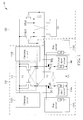
- FIG. 1 is a diagram of an apparatus for performing level shift control in an electronic device according to an embodiment of the present invention, where the apparatus 100 comprises at least one portion (e.g. a portion or all) of the electronic device.
- the apparatus 100 may comprise a portion of the electronic device mentioned above, and more particularly, can be at least one hardware circuit such as at least one integrated circuit (IC) within the electronic device.
- the apparatus 100 can be the whole of the electronic device mentioned above.
- the apparatus 100 may comprise a system comprising the electronic device mentioned above (e.g. an audio/video system comprising the electronic device).
- Examples of the electronic device may include, but not limited to, a mobile phone (e.g. a multifunctional mobile phone), tablet, and a personal computer such as a laptop computer.
- the apparatus 100 may comprise an input stage 110 that is positioned in a level shifter of the electronic device, and further comprises an output stage 120 that is positioned in the level shifter and coupled to the input stage 110 through a set of intermediate nodes A and B.
- the input stage 110 may comprise a switching circuit 111, a set of clamping circuits 112A and 112B, and a hybrid current control circuit, which may comprise a set of switching units M1 and M2, an inverter coupled between the set of switching units M1 and M2, a set of virtual short circuits 114A and 114B, and a set of bias circuits 118A and 118B in this embodiment, where the set of switching units M1 and M2 can be implemented with two Metal Oxide Semiconductor Field Effect Transistors (MOSFETs) such as two N-type MOSFETs (NMOSFETs), and the shaded portion illustrated on the uppermost of each of the set of switching units M1 and M2 may indicate that they can be implemented as high voltage (HV) devices having large parasitic capacitance.
- MOSFETs Metal Oxide Semiconductor Field Effect Transistors
- NMOSFETs N-type MOSFETs
- the output stage 120 may comprise some switching units and associated wirings, such as those shown around the rightmost of FIG. 1 .
- some P-type MOSFETs such as those within the switching circuit 111 and those within in the output stage 120 are utilized for selectively coupling associated nodes or terminals to the reference voltage level V2, respectively
- some NMOSFETs such as those within the set of switching units M1 and M2 are utilized for selectively coupling associated nodes or terminals to the reference voltage level G1, respectively
- some NMOSFETs such as those within in the output stage 120 are utilized for selectively coupling associated nodes or terminals to the reference voltage level G2, respectively.
- implementations of these switching components are not limited to be NMOSFETs or PMOSFETs.
- connection of the body bias of a MOSFET such as that of any of these switching components are not limited to be the corresponding connection shown in FIG. 1 .
- the input stage 110 may be arranged for receiving at least one input signal of the level shifter through at least one input terminal of the input stage 110, such as the input terminal IN, and controlling voltage levels of the set of intermediate nodes A and B according to the aforementioned at least one input signal.
- the inverter coupled between the set of switching units M1 and M2, and more particularly, coupled between the input terminals IN and INB may be supplied by the reference voltage levels V1 and G1, and may invert the input signal at the input terminal IN to generate another input signal at the input terminal INB, such as an inverted signal of the input signal at the input terminal IN, where the input terminal IN is arranged to receive the aforementioned at least one input signal, and the input terminal INB is arranged to receive the inverted signal.
- the input stage 110 may comprises a set of switching units coupled to the aforementioned at least one input terminal, such as the PMOSFETs within the switching circuit 111 shown in FIG.
- this set of switching units may be arranged for controlling the voltage levels of the set of intermediate nodes A and B in response to the aforementioned at least one input signal.
- a switching unit of this set of switching units may selectively couple one of the set of intermediate nodes A and B to a predetermined voltage level supplied to the level shifter, such as the reference voltage level V2 in this embodiment.
- the output stage 120 may be arranged for driving at least one output signal of the level shifter through at least one output terminal of the output stage 120, such as the output terminal INLS, and controlling at least one voltage level of the at least one output terminal according to the voltage levels of the set of intermediate nodes A and B.
- the output signal at the output terminal INLS can be regarded as an inverted version of another output signal at the output terminal INBLS, and vice versa.
- the hybrid current control circuit which may comprise the set of switching units M1 and M2, the inverter mentioned above, the set of virtual short circuits 114A and 114B, and the set of bias circuits 118A and 118B in this embodiment, is coupled to the aforementioned at least one input terminal such as the input terminal IN.
- This hybrid current control circuit may be arranged for performing current control for the input stage 110, and may operate in response to the input signal received from the input terminal IN.
- the virtual short circuits 114A and 114B can be utilized for performing virtual short operations for the terminals AA and BB to their ground (e.g.
- the hybrid current control circuit is equipped with multiple sets of parallel paths, such as some sub-paths (labeled "SP" in FIG. 1 , for brevity), for controlling currents passing through the set of intermediate nodes A and B, respectively, where a set of parallel paths within the aforementioned multiple sets of parallel paths may comprise signal paths (or sub-paths) that are electrically connected in parallel.
- the input stage 110 may comprise at least one sub-path (e.g.
- the input stage 110 may comprise at least one sub-path (e.g. one or more sub-paths) in the virtual short circuit 114B and may comprise at least one sub-path (e.g. one or more sub-paths) in the bias circuit 118B, and these sub-paths and/or their extended signal paths may be connected in parallel within this hybrid current control circuit.
- the input stage 110 may comprise at least one sub-path (e.g. one or more sub-paths) in the virtual short circuit 114B and may comprise at least one sub-path (e.g. one or more sub-paths) in the bias circuit 118B, and these sub-paths and/or their extended signal paths may be connected in parallel within this hybrid current control circuit.
- each set of the aforementioned multiple sets of parallel paths may comprise a first path on which a first switching unit and at least one passive component are positioned, and may further comprise a second path on which a second switching unit is positioned.
- the first switching unit and the second switching unit can be controlled by different control signals, respectively.
- the input stage 110 may comprise a plurality of switching units, each of which is positioned on a path within the multiple sets of parallel paths, where the plurality of switching units may comprise the first switching unit on the first path and the second switching unit on the second path. This is for illustrative purposes only, and is not meant to be a limitation of the present invention.
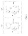
- FIG. 2 illustrates the set of clamping circuits 112A and 112B involved with the apparatus 100 shown in FIG. 1 according to an embodiment of the present invention.
- This set of clamping circuits 112A and 112B may be positioned in the level shifter and respectively coupled to the set of intermediate nodes A and B, and may be arranged for clamping the voltage levels of the set of intermediate nodes A and B, respectively.
- some PMOSFETs such as those within the clamping circuits 112A and 112B are utilized for selectively coupling associated nodes or terminals to the reference voltage level V2, respectively. This is for illustrative purposes only, and is not meant to be a limitation of the present invention.
- implementations of these switching components are not limited to be PMOSFETs.
- the connection of the body bias of a MOSFET such as that of any of these switching components are not limited to be the corresponding connection shown in FIG. 2 .
- FIG. 3 illustrates some implementation details of the multiple sets of parallel paths involved with the apparatus 100 shown in FIG. 1 according to an embodiment of the present invention.
- the aforementioned hybrid current control circuit may comprise a plurality of capacitors C1 and C2, at least one capacitor of which may be positioned on the first path of this embodiment and is utilized as the aforementioned at least one passive component in this embodiment.
- the hybrid current control circuit may further comprise a plurality of current sources I1 and I2, at least one current source of which may be positioned on the second path of this embodiment.
- the hybrid current control circuit may further comprise a plurality of resistors R1 and R2, at least one resistor of which may be positioned on the second path of this embodiment.
- the hybrid current control circuit may further comprise other switching units such as those positioned in the set of virtual short circuits 114A and 114B and the set of bias circuits 118A and 118B, respectively, where these switching units (e.g. the switching units M3, M4, etc.) can also be implemented with MOSFETs such as NMOSFETs, and the shaded portion illustrated on the uppermost of each of the switching units M3 and M4 may indicate that they can be implemented as HV devices having large parasitic capacitance.
- these switching units e.g. the switching units M3, M4, etc.
- MOSFETs such as NMOSFETs
- a first set of parallel paths within the multiple sets of parallel paths may be arranged for controlling the current passing through one intermediate node within the set of intermediate nodes A and B, such as the intermediate node A, and a second set of parallel paths within the multiple sets of parallel paths may be arranged for controlling the current passing through another intermediate node within the set of intermediate nodes A and B, such as the intermediate node B.
- the aforementioned first path may represent the signal path passing through the switching unit M1 and the virtual short circuit 114A
- the aforementioned second path may represent the signal path passing through the bias circuit 118A
- the aforementioned at least one passive component may represent the capacitor C1
- the first switching unit such as the switching unit M1 and the second switching unit such as the switching unit M3 can be controlled by different control signals at the terminals IN and INX, respectively.
- the aforementioned first path may represent the signal path passing through the switching unit M2 and the virtual short circuit 114B
- the aforementioned second path may represent the signal path passing through the bias circuit 118B
- the aforementioned at least one passive component may represent the capacitor C2
- the first switching unit such as the switching unit M2 and the second switching unit such as the switching unit M4 can be controlled by different control signals at the terminals INB and INBX, respectively.
- some NMOSFETs such as those within the switching units M1 and M2, the virtual short circuits 114A and 114B, and the bias circuits 118A and 118B are utilized for selectively coupling associated nodes or terminals to the reference voltage level G1, respectively.
- this is for illustrative purposes only, and is not meant to be a limitation of the present invention.
- implementations of these switching components are not limited to be NMOSFETs.
- the connection of the body bias of a MOSFET such as that of any of these switching components are not limited to be the corresponding connection shown in FIG. 3 .
- FIG. 4 illustrates some implementation details of the multiple sets of parallel paths involved with the apparatus 100 shown in FIG. 1 according to another embodiment of the present invention.
- the resistors R1 and R2 can be removed in this embodiment.
- similar descriptions for this embodiment are not repeated in detail here.
- FIG. 5 illustrates some implementation details of the multiple sets of parallel paths involved with the apparatus 100 shown in FIG. 1 according to another embodiment of the present invention.
- the current sources I1 and I2 can be removed in this embodiment.
- similar descriptions for this embodiment are not repeated in detail here.
- FIG. 6 illustrates some implementation details of the multiple sets of parallel paths involved with the apparatus 100 shown in FIG. 1 according to another embodiment of the present invention.
- the resistors R1 and R2 and the current sources I1 and I2 can be removed in this embodiment.
- similar descriptions for this embodiment are not repeated in detail here.
- FIG. 7 illustrates some implementation details of the multiple sets of parallel paths involved with the apparatus 100 shown in FIG. 1 according to another embodiment of the present invention.
- the resistors R1 and R2 and the current sources I1 and I2 can be removed in this embodiment.
- the switching unit within the bias circuit 118A and the switching unit within the bias circuit 118B have been changed to have other connection arrangements, respectively, so as to be controlled by the input signal at the input terminal IN and the input signal at the input terminal INB, respectively.
- the switching unit within the bias circuit 118A and the switching unit within the bias circuit 118B are HV devices. For brevity, similar descriptions for this embodiment are not repeated in detail here.
- the first path may comprise two sub-paths that are connected in parallel (e.g. the sub-paths below the terminal AA, or the sub-paths below the terminal BB, in any of these embodiments), and the aforementioned at least one passive component (e.g. the capacitor C1, or the capacitor C2) may be positioned on one sub-path within the two sub-paths.
- the aforementioned hybrid current control circuit may comprise another switching unit (e.g. the switching unit connected in parallel with the capacitor C1, or the switching unit connected in parallel with the capacitor C2) that is positioned on another sub-path within the two sub-paths.
- the first switching unit may be controlled by a first control signal within the control signals
- the second switching unit may be controlled by a second control signal within the control signals
- the other switching unit may be controlled by the inverted signal of the first control signal.
- the first path may comprise two sub-paths that are connected in parallel (e.g. the sub-paths respectively passing through the components of the virtual short circuit 114A, or the sub-paths respectively passing through the components of the virtual short circuit 114B, in any of these embodiments).
- the aforementioned at least one passive component e.g.
- the capacitor C1, or the capacitor C2) may be positioned on one sub-path within the two sub-paths
- the first switching unit e.g. the switching unit connected in parallel with the capacitor C1 and positioned within the virtual short circuit 114A, or the switching unit connected in parallel with the capacitor C2 and positioned within the virtual short circuit 114B
- the second path and the two sub-paths are connected in parallel.
- the first switching unit may be controlled by a first control signal within the control signals
- the second switching unit is controlled by a second control signal within the control signals, where one control signal within the first control signal and the second control signal is an inverted signal of another control signal within the first control signal and the second control signal.
- FIG. 8 illustrates a set of voltage detection modules 116A and 116B involved with the apparatus 100 shown in FIG. 1 according to an embodiment of the present invention.
- the aforementioned first switching unit e.g. the switching unit M1, or the switching unit M2
- the aforementioned second switching unit e.g. the switching unit M3, or the switching unit M4
- the switching unit M1 may be controlled by the input signal at the input terminal IN
- the switching unit M3 may be controlled by the signal at the terminal INX, such as the output of the voltage detection module 116A
- the switching unit M2 may be controlled by the input signal at the input terminal INB
- the switching unit M4 may be controlled by the signal at the terminal INBX, such as the output of the voltage detection module 116B.
- the input stage 110 may comprise this set of voltage detection modules 116A and 116B, and a voltage detection module within the set of voltage detection modules 116A and 116B may be coupled between the first switching unit and the second switching unit mentioned above.
- this voltage detection module such as the voltage detection module 116A or the voltage detection module 116B, may be arranged for detecting a voltage level at a node (e.g. the terminal AA for the detection of the voltage detection module 116A, or the terminal BB for the detection of the voltage detection module 116B) between the first switching unit (e.g. the switching unit M1, or the switching unit M2) and the aforementioned at least one passive component (e.g.
- the voltage detection module 116A may detect the voltage level at the terminal AA between the switching unit M1 and the capacitor C1, to generate the control signal INX according to the voltage level at the terminal AA.
- the voltage detection module 116B may detect the voltage level at the terminal BB between the switching unit M2 and the capacitor C2, to generate the control signal INBX according to the voltage level at the terminal BB.
- this voltage detection module such as the voltage detection module 116A or the voltage detection module 116B, may comprise a plurality of MOSFETs (e.g. the PMOSFET and the NMOSFETs within the voltage detection module 116A, or the PMOSFET and the NMOSFETs within the voltage detection module 116B), at least one of which is coupled to this node (e.g. the terminal AA, or the terminal BB) to detect the voltage level at this node, and these MOSFETs may be arranged for performing switching control operations within this voltage detection module, respectively.
- MOSFETs e.g. the PMOSFET and the NMOSFETs within the voltage detection module 116A, or the PMOSFET and the NMOSFETs within the voltage detection module 116B
- the MOSFETs in the voltage detection module 116A are electrically connected to the terminal AA directly or indirectly, and the switching operation of at least one of these MOSFETs may be controlled in response to the voltage level at the terminal AA.
- the MOSFETs in the voltage detection module 116B are electrically connected to the terminal BB directly or indirectly, and the switching operation of at least one of these MOSFETs may be controlled in response to the voltage level at the terminal BB.
- this voltage detection module such as the voltage detection module 116A or the voltage detection module 116B, may further comprise a plurality of current sources (e.g.
- a node e.g. the terminal INX, or the terminal INBX
- the apparatus 100 may be equipped with this set of voltage detection modules 116A and 116B.
- a turn-on time of the second switching unit under control of the second control signal may be less than a turn-on time of the first switching unit under control of the first control signal.
- the turn-on time of the second switching unit under control of the second control signal may be selectively suppressed to be zero.
- this set of voltage detection modules 116A and 116B may be replaced by other component(s).
- the first switching unit e.g. the switching unit M1, or the switching unit M2
- the first control signal e.g. the input signal at the input terminal IN, or the input signal at the input terminal INB
- the second switching unit e.g. the switching unit M3, or the switching unit M4
- the second control signal e.g. the signal at the terminal INX, or the signal at the terminal INBX
- the input stage 110 may comprise a control signal generator that is coupled to the second switching unit in these embodiments, and this control signal generator may be arranged for generating the second control signal by converting the first control signal into the second control signal.
- the aforementioned turn-on time of the second switching unit under control of the second control signal may be less than the aforementioned turn-on time of the first switching unit under control of the first control signal.
- the turn-on time of the second switching unit under control of the second control signal may be selectively suppressed to be zero.
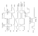
- FIG. 9 illustrates a timing chart of associated signals involved with the apparatus 100 shown in FIG. 1 according to an embodiment of the present invention, where these signals are depicted with waveforms at the associated terminals or nodes, such as the input terminals IN and INB, the terminals AA and BB, the intermediate nodes A and B, and the terminals INX and INBX, and therefore can be labeled with the same names of these terminals or nodes, respectively.
- the associated terminals or nodes such as the input terminals IN and INB, the terminals AA and BB, the intermediate nodes A and B, and the terminals INX and INBX, and therefore can be labeled with the same names of these terminals or nodes, respectively.
- the low level GND of any signal within the input signals at the input terminals IN and INB and the signals at the terminals AA and BB can be equivalent to the reference voltage level G1
- the high level and the low level of any signal within the signals at the intermediate nodes A and B can be equivalent to the boot voltage VBOOT and the boot voltage minus 2 Volts (V) (i.e. the voltage level of (VBOOT - 2V) in this embodiment), respectively.
- the aforementioned turn-on time of the second switching unit (e.g. the switching unit M3, or the switching unit M4) under control of the second control signal may be less than the aforementioned turn-on time of the first switching unit (e.g. the switching unit M1, or the switching unit M2) under control of the first control signal.
- the turn-on time T_INX_ON(2) of the switching unit M3 under control of the control signal at the terminal INX is less than the turn-on time T_IN_ON(2) of the switching unit M1 under control of the input signal at the input terminal IN.
- the turn-on time T_INB_ON(2) of the switching unit M4 under control of the control signal at the terminal INBX is less than the turn-on time T_INB_ON(2) of the switching unit M2 under control of the input signal at the input terminal INB.
- the turn-on time of the second switching unit e.g. the switching unit M3, or the switching unit M4 under control of the second control signal.
- the turn-on time of the switching unit M3 under control of the control signal at the terminal INX has been suppressed to be zero, since the voltage level of the control signal at the terminal INX is kept at the low level thereof within this period.
- the turn-on time of the switching unit M4 under control of the control signal at the terminal INBX has been suppressed to be zero, since the voltage level of the control signal at the terminal INBX is kept at the low level thereof within this period.
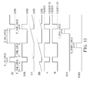
- FIG. 10 illustrates a timing chart of associated signals involved with the apparatus 100 shown in FIG. 1 according to another embodiment of the present invention, where these signals are depicted with waveforms at the associated terminals or nodes, such as the input terminals IN and INB, the terminals AA and BB, the intermediate nodes A and B, and the terminals INX and INBX, and therefore can be labeled with the same names of these terminals or nodes, respectively.
- this embodiment may be used for illustrating discharge current on time reduction.
- the capacitance values of the capacitors C1 and C2 may be increased, respectively, to achieve a lower slew rate for better quiescent current of the boot voltage VBOOT in this embodiment.
- the aforementioned turn-on time of the second switching unit (e.g. the switching unit M3, or the switching unit M4) under control of the second control signal may be less than the aforementioned turn-on time of the first switching unit (e.g. the switching unit M1, or the switching unit M2) under control of the first control signal.
- the turn-on time T_INX_ON(2) of the switching unit M3 under control of the control signal at the terminal INX is less than the turn-on time T_IN_ON(2) of the switching unit M1 under control of the input signal at the input terminal IN.
- the turn-on time T_INB_ON(2) of the switching unit M4 under control of the control signal at the terminal INBX is less than the turn-on time T_INB_ON(2) of the switching unit M2 under control of the input signal at the input terminal INB.
- the turn-on time of the second switching unit e.g. the switching unit M3, or the switching unit M4 under control of the second control signal.
- the turn-on time of the switching unit M3 under control of the control signal at the terminal INX has been suppressed to be zero, since the voltage level of the control signal at the terminal INX is kept at the low level thereof within this period.
- the turn-on time of the switching unit M4 under control of the control signal at the terminal INBX has been suppressed to be zero, since the voltage level of the control signal at the terminal INBX is kept at the low level thereof within this period.
- each set of the multiple sets of parallel paths may comprise a first path on which a first switching unit is positioned (e.g. the signal path passing through the switching unit connected in parallel with the virtual short circuit 114A and positioned within the bias circuit 118A, or the signal path passing through the switching unit connected in parallel with the virtual short circuit 114B and positioned within the bias circuit 118B), and may comprise a second path on which a second switching unit is positioned (e.g.
- the first switching unit and the second switching unit can be controlled by different control signals, respectively.
- the aforementioned at least one input signal may correspond to a first power domain
- the aforementioned at least one output signal may correspond to a second power domain
- these four switching units M1, M2, M3, and M4 can be implemented as HV devices having large parasitic capacitance.
- the apparatus 100 may comprise at least one voltage detector such as the set of voltage detection modules 116A and 116B shown in FIG. 8 , for check the voltage levels at the terminals AA and BB, in order to control the discharging time of the corresponding signal path(s) within the bias circuit 118A (e.g.
- the sub-path passing through the current source I1 and/or the sub-path passing through the resistor R1) and the discharging time of the corresponding signal path(s) within the bias circuit 118B e.g. the sub-path passing through the current source I2 and/or the sub-path passing through the resistor R2.
Landscapes
- Engineering & Computer Science (AREA)
- Computer Hardware Design (AREA)
- Physics & Mathematics (AREA)
- Computing Systems (AREA)
- General Engineering & Computer Science (AREA)
- Mathematical Physics (AREA)
- Logic Circuits (AREA)
- Electronic Switches (AREA)
Applications Claiming Priority (2)
| Application Number | Priority Date | Filing Date | Title |
|---|---|---|---|
| US201562131262P | 2015-03-11 | 2015-03-11 | |
| US14/830,744 US9838015B2 (en) | 2015-03-11 | 2015-08-20 | Apparatus for performing level shift control in an electronic device with aid of parallel paths controlled by different control signals for current control purposes |
Publications (3)
| Publication Number | Publication Date |
|---|---|
| EP3068050A2 true EP3068050A2 (de) | 2016-09-14 |
| EP3068050A3 EP3068050A3 (de) | 2016-11-30 |
| EP3068050B1 EP3068050B1 (de) | 2018-03-21 |
Family
ID=54251941
Family Applications (1)
| Application Number | Title | Priority Date | Filing Date |
|---|---|---|---|
| EP15186370.1A Active EP3068050B1 (de) | 2015-03-11 | 2015-09-23 | Vorrichtung zur durchführung von pegelschieberschaltungssteuerung in einer elektronischen vorrichtung mithilfe paralleler, durch verschiedene steuerungssignale für stromregelzwecke gesteuerter pfade |
Country Status (3)
| Country | Link |
|---|---|
| US (1) | US9838015B2 (de) |
| EP (1) | EP3068050B1 (de) |
| CN (1) | CN105978549B (de) |
Families Citing this family (2)
| Publication number | Priority date | Publication date | Assignee | Title |
|---|---|---|---|---|
| US11196420B1 (en) * | 2020-07-15 | 2021-12-07 | Samsung Electronics Co., Ltd. | Level shifter |
| US20250274124A1 (en) * | 2024-02-28 | 2025-08-28 | Taiwan Semiconductor Manufacturing Company Ltd. | Level shifter with independent driver |
Citations (1)
| Publication number | Priority date | Publication date | Assignee | Title |
|---|---|---|---|---|
| US7839197B2 (en) | 2007-09-11 | 2010-11-23 | Richtek Technology Corp. | Level shift circuit |
Family Cites Families (9)
| Publication number | Priority date | Publication date | Assignee | Title |
|---|---|---|---|---|
| US5896043A (en) | 1989-02-10 | 1999-04-20 | Fuji Electric Co., Ltd. | Level shift circuit |
| US20050134355A1 (en) * | 2003-12-18 | 2005-06-23 | Masato Maede | Level shift circuit |
| DE102006014355B3 (de) | 2006-03-28 | 2007-06-06 | Infineon Technologies Ag | Stromgesteuerter Pegelumsetzer mit Signalrückkopplung |
| JP5203791B2 (ja) * | 2008-04-18 | 2013-06-05 | ルネサスエレクトロニクス株式会社 | レベルシフト回路 |
| DE102008056131A1 (de) * | 2008-11-06 | 2010-05-12 | Micronas Gmbh | Pegelschieber mit Natural-Transistoren |
| CN102510277B (zh) * | 2011-12-31 | 2014-04-09 | 杭州士兰微电子股份有限公司 | 一种mosfet驱动电路 |
| US8907712B2 (en) * | 2012-03-27 | 2014-12-09 | Mediatek Inc. | Level shifter circuits capable of dealing with extreme input signal level voltage drops and compensating for device PVT variation |
| WO2014020724A1 (ja) * | 2012-08-01 | 2014-02-06 | ルネサスエレクトロニクス株式会社 | レベルシフト回路、半導体装置 |
| US9264022B2 (en) | 2013-04-18 | 2016-02-16 | Sharp Kabushiki Kaisha | Level shift circuit |
-
2015
- 2015-08-20 US US14/830,744 patent/US9838015B2/en active Active
- 2015-09-23 EP EP15186370.1A patent/EP3068050B1/de active Active
- 2015-11-16 CN CN201510784363.3A patent/CN105978549B/zh active Active
Patent Citations (1)
| Publication number | Priority date | Publication date | Assignee | Title |
|---|---|---|---|---|
| US7839197B2 (en) | 2007-09-11 | 2010-11-23 | Richtek Technology Corp. | Level shift circuit |
Also Published As
| Publication number | Publication date |
|---|---|
| EP3068050A3 (de) | 2016-11-30 |
| CN105978549B (zh) | 2019-04-19 |
| CN105978549A (zh) | 2016-09-28 |
| US9838015B2 (en) | 2017-12-05 |
| EP3068050B1 (de) | 2018-03-21 |
| US20160269028A1 (en) | 2016-09-15 |
Similar Documents
| Publication | Publication Date | Title |
|---|---|---|
| US7750717B2 (en) | Single supply level shifter circuit for multi-voltage designs, capable of up/down shifting | |
| JP4874887B2 (ja) | 高周波半導体スイッチ装置 | |
| US10536142B2 (en) | Power on reset circuit | |
| US9641166B2 (en) | Bootstrapped switching circuit with fast turn-on | |
| US20090015974A1 (en) | Esd detection circuit | |
| CN107819468A (zh) | 自举开关电路 | |
| US10756728B2 (en) | Insulated gate device drive apparatus | |
| US10128835B2 (en) | Aging tolerant I/O driver | |
| JP2013172482A (ja) | スイッチ制御回路、半導体装置および無線通信装置 | |
| US8963638B2 (en) | Operational amplifier circuit | |
| US20030062937A1 (en) | Output circuit for adjusting output voltage slew rate | |
| EP3068050B1 (de) | Vorrichtung zur durchführung von pegelschieberschaltungssteuerung in einer elektronischen vorrichtung mithilfe paralleler, durch verschiedene steuerungssignale für stromregelzwecke gesteuerter pfade | |
| KR20100033876A (ko) | 듀티 제어회로 및 이를 구비하는 반도체 장치 | |
| EP3046239B1 (de) | Stromgeneratorschaltung, verfahren zur stromerzeugung, ladungspumpenschaltung und ladungspumpenverfahren | |
| JP2013172189A (ja) | スイッチ制御回路、半導体装置および無線通信装置 | |
| JP2009170987A (ja) | 電力増幅回路 | |
| US20160269023A1 (en) | Semiconductor switch and switching system | |
| JP5221739B2 (ja) | 高周波半導体スイッチ装置 | |
| JP7378663B2 (ja) | デジタルアナログ変換機 | |
| US9537489B1 (en) | Level shifter with dynamic bias technique under overstress voltage | |
| US8450987B2 (en) | Switching apparatus and control signal generator thereof | |
| US9473142B2 (en) | Method for performing signal driving control in an electronic device with aid of driving control signals, and associated apparatus | |
| US20130135037A1 (en) | Voltage multiplying circuit, signal switch chip and impedance adjusting method thereof | |
| US9755582B2 (en) | Switch circuit, sampling switch circuit and switch capacitor circuit | |
| US11736094B2 (en) | Filter circuit and semiconductor device |
Legal Events
| Date | Code | Title | Description |
|---|---|---|---|
| PUAI | Public reference made under article 153(3) epc to a published international application that has entered the european phase |
Free format text: ORIGINAL CODE: 0009012 |
|
| AK | Designated contracting states |
Kind code of ref document: A2 Designated state(s): AL AT BE BG CH CY CZ DE DK EE ES FI FR GB GR HR HU IE IS IT LI LT LU LV MC MK MT NL NO PL PT RO RS SE SI SK SM TR |
|
| AX | Request for extension of the european patent |
Extension state: BA ME |
|
| PUAL | Search report despatched |
Free format text: ORIGINAL CODE: 0009013 |
|
| AK | Designated contracting states |
Kind code of ref document: A3 Designated state(s): AL AT BE BG CH CY CZ DE DK EE ES FI FR GB GR HR HU IE IS IT LI LT LU LV MC MK MT NL NO PL PT RO RS SE SI SK SM TR |
|
| AX | Request for extension of the european patent |
Extension state: BA ME |
|
| RIC1 | Information provided on ipc code assigned before grant |
Ipc: H03K 19/00 20060101ALI20161026BHEP Ipc: H03K 3/012 20060101AFI20161026BHEP Ipc: H03K 3/356 20060101ALI20161026BHEP |
|
| 17P | Request for examination filed |
Effective date: 20170209 |
|
| RBV | Designated contracting states (corrected) |
Designated state(s): AL AT BE BG CH CY CZ DE DK EE ES FI FR GB GR HR HU IE IS IT LI LT LU LV MC MK MT NL NO PL PT RO RS SE SI SK SM TR |
|
| 17Q | First examination report despatched |
Effective date: 20170426 |
|
| REG | Reference to a national code |
Ref country code: DE Ref legal event code: R079 Ref document number: 602015009019 Country of ref document: DE Free format text: PREVIOUS MAIN CLASS: H03K0003012000 Ipc: H03K0019003000 |
|
| RIC1 | Information provided on ipc code assigned before grant |
Ipc: H03K 3/356 20060101ALI20171108BHEP Ipc: H03K 3/012 20060101ALI20171108BHEP Ipc: H03K 19/00 20060101ALI20171108BHEP Ipc: H03K 19/003 20060101AFI20171108BHEP Ipc: H03K 19/0185 20060101ALI20171108BHEP |
|
| GRAP | Despatch of communication of intention to grant a patent |
Free format text: ORIGINAL CODE: EPIDOSNIGR1 |
|
| INTG | Intention to grant announced |
Effective date: 20171219 |
|
| GRAS | Grant fee paid |
Free format text: ORIGINAL CODE: EPIDOSNIGR3 |
|
| RIN1 | Information on inventor provided before grant (corrected) |
Inventor name: KUNG, NIEN-HUI |
|
| GRAA | (expected) grant |
Free format text: ORIGINAL CODE: 0009210 |
|
| AK | Designated contracting states |
Kind code of ref document: B1 Designated state(s): AL AT BE BG CH CY CZ DE DK EE ES FI FR GB GR HR HU IE IS IT LI LT LU LV MC MK MT NL NO PL PT RO RS SE SI SK SM TR |
|
| REG | Reference to a national code |
Ref country code: GB Ref legal event code: FG4D |
|
| REG | Reference to a national code |
Ref country code: CH Ref legal event code: EP |
|
| REG | Reference to a national code |
Ref country code: AT Ref legal event code: REF Ref document number: 982147 Country of ref document: AT Kind code of ref document: T Effective date: 20180415 |
|
| REG | Reference to a national code |
Ref country code: IE Ref legal event code: FG4D |
|
| REG | Reference to a national code |
Ref country code: DE Ref legal event code: R096 Ref document number: 602015009019 Country of ref document: DE |
|
| REG | Reference to a national code |
Ref country code: NL Ref legal event code: MP Effective date: 20180321 |
|
| PG25 | Lapsed in a contracting state [announced via postgrant information from national office to epo] |
Ref country code: CY Free format text: LAPSE BECAUSE OF FAILURE TO SUBMIT A TRANSLATION OF THE DESCRIPTION OR TO PAY THE FEE WITHIN THE PRESCRIBED TIME-LIMIT Effective date: 20180321 Ref country code: FI Free format text: LAPSE BECAUSE OF FAILURE TO SUBMIT A TRANSLATION OF THE DESCRIPTION OR TO PAY THE FEE WITHIN THE PRESCRIBED TIME-LIMIT Effective date: 20180321 Ref country code: NO Free format text: LAPSE BECAUSE OF FAILURE TO SUBMIT A TRANSLATION OF THE DESCRIPTION OR TO PAY THE FEE WITHIN THE PRESCRIBED TIME-LIMIT Effective date: 20180621 Ref country code: LT Free format text: LAPSE BECAUSE OF FAILURE TO SUBMIT A TRANSLATION OF THE DESCRIPTION OR TO PAY THE FEE WITHIN THE PRESCRIBED TIME-LIMIT Effective date: 20180321 Ref country code: HR Free format text: LAPSE BECAUSE OF FAILURE TO SUBMIT A TRANSLATION OF THE DESCRIPTION OR TO PAY THE FEE WITHIN THE PRESCRIBED TIME-LIMIT Effective date: 20180321 |
|
| REG | Reference to a national code |
Ref country code: LT Ref legal event code: MG4D |
|
| REG | Reference to a national code |
Ref country code: AT Ref legal event code: MK05 Ref document number: 982147 Country of ref document: AT Kind code of ref document: T Effective date: 20180321 |
|
| PG25 | Lapsed in a contracting state [announced via postgrant information from national office to epo] |
Ref country code: LV Free format text: LAPSE BECAUSE OF FAILURE TO SUBMIT A TRANSLATION OF THE DESCRIPTION OR TO PAY THE FEE WITHIN THE PRESCRIBED TIME-LIMIT Effective date: 20180321 Ref country code: SE Free format text: LAPSE BECAUSE OF FAILURE TO SUBMIT A TRANSLATION OF THE DESCRIPTION OR TO PAY THE FEE WITHIN THE PRESCRIBED TIME-LIMIT Effective date: 20180321 Ref country code: RS Free format text: LAPSE BECAUSE OF FAILURE TO SUBMIT A TRANSLATION OF THE DESCRIPTION OR TO PAY THE FEE WITHIN THE PRESCRIBED TIME-LIMIT Effective date: 20180321 Ref country code: BG Free format text: LAPSE BECAUSE OF FAILURE TO SUBMIT A TRANSLATION OF THE DESCRIPTION OR TO PAY THE FEE WITHIN THE PRESCRIBED TIME-LIMIT Effective date: 20180621 Ref country code: GR Free format text: LAPSE BECAUSE OF FAILURE TO SUBMIT A TRANSLATION OF THE DESCRIPTION OR TO PAY THE FEE WITHIN THE PRESCRIBED TIME-LIMIT Effective date: 20180622 |
|
| REG | Reference to a national code |
Ref country code: FR Ref legal event code: PLFP Year of fee payment: 4 |
|
| PG25 | Lapsed in a contracting state [announced via postgrant information from national office to epo] |
Ref country code: IT Free format text: LAPSE BECAUSE OF FAILURE TO SUBMIT A TRANSLATION OF THE DESCRIPTION OR TO PAY THE FEE WITHIN THE PRESCRIBED TIME-LIMIT Effective date: 20180321 Ref country code: ES Free format text: LAPSE BECAUSE OF FAILURE TO SUBMIT A TRANSLATION OF THE DESCRIPTION OR TO PAY THE FEE WITHIN THE PRESCRIBED TIME-LIMIT Effective date: 20180321 Ref country code: RO Free format text: LAPSE BECAUSE OF FAILURE TO SUBMIT A TRANSLATION OF THE DESCRIPTION OR TO PAY THE FEE WITHIN THE PRESCRIBED TIME-LIMIT Effective date: 20180321 Ref country code: NL Free format text: LAPSE BECAUSE OF FAILURE TO SUBMIT A TRANSLATION OF THE DESCRIPTION OR TO PAY THE FEE WITHIN THE PRESCRIBED TIME-LIMIT Effective date: 20180321 Ref country code: EE Free format text: LAPSE BECAUSE OF FAILURE TO SUBMIT A TRANSLATION OF THE DESCRIPTION OR TO PAY THE FEE WITHIN THE PRESCRIBED TIME-LIMIT Effective date: 20180321 Ref country code: PL Free format text: LAPSE BECAUSE OF FAILURE TO SUBMIT A TRANSLATION OF THE DESCRIPTION OR TO PAY THE FEE WITHIN THE PRESCRIBED TIME-LIMIT Effective date: 20180321 Ref country code: AL Free format text: LAPSE BECAUSE OF FAILURE TO SUBMIT A TRANSLATION OF THE DESCRIPTION OR TO PAY THE FEE WITHIN THE PRESCRIBED TIME-LIMIT Effective date: 20180321 |
|
| PG25 | Lapsed in a contracting state [announced via postgrant information from national office to epo] |
Ref country code: AT Free format text: LAPSE BECAUSE OF FAILURE TO SUBMIT A TRANSLATION OF THE DESCRIPTION OR TO PAY THE FEE WITHIN THE PRESCRIBED TIME-LIMIT Effective date: 20180321 Ref country code: SM Free format text: LAPSE BECAUSE OF FAILURE TO SUBMIT A TRANSLATION OF THE DESCRIPTION OR TO PAY THE FEE WITHIN THE PRESCRIBED TIME-LIMIT Effective date: 20180321 Ref country code: SK Free format text: LAPSE BECAUSE OF FAILURE TO SUBMIT A TRANSLATION OF THE DESCRIPTION OR TO PAY THE FEE WITHIN THE PRESCRIBED TIME-LIMIT Effective date: 20180321 Ref country code: CZ Free format text: LAPSE BECAUSE OF FAILURE TO SUBMIT A TRANSLATION OF THE DESCRIPTION OR TO PAY THE FEE WITHIN THE PRESCRIBED TIME-LIMIT Effective date: 20180321 |
|
| PG25 | Lapsed in a contracting state [announced via postgrant information from national office to epo] |
Ref country code: PT Free format text: LAPSE BECAUSE OF FAILURE TO SUBMIT A TRANSLATION OF THE DESCRIPTION OR TO PAY THE FEE WITHIN THE PRESCRIBED TIME-LIMIT Effective date: 20180723 |
|
| REG | Reference to a national code |
Ref country code: DE Ref legal event code: R097 Ref document number: 602015009019 Country of ref document: DE |
|
| PLBE | No opposition filed within time limit |
Free format text: ORIGINAL CODE: 0009261 |
|
| STAA | Information on the status of an ep patent application or granted ep patent |
Free format text: STATUS: NO OPPOSITION FILED WITHIN TIME LIMIT |
|
| PG25 | Lapsed in a contracting state [announced via postgrant information from national office to epo] |
Ref country code: DK Free format text: LAPSE BECAUSE OF FAILURE TO SUBMIT A TRANSLATION OF THE DESCRIPTION OR TO PAY THE FEE WITHIN THE PRESCRIBED TIME-LIMIT Effective date: 20180321 |
|
| 26N | No opposition filed |
Effective date: 20190102 |
|
| PG25 | Lapsed in a contracting state [announced via postgrant information from national office to epo] |
Ref country code: MC Free format text: LAPSE BECAUSE OF FAILURE TO SUBMIT A TRANSLATION OF THE DESCRIPTION OR TO PAY THE FEE WITHIN THE PRESCRIBED TIME-LIMIT Effective date: 20180321 |
|
| REG | Reference to a national code |
Ref country code: CH Ref legal event code: PL |
|
| PG25 | Lapsed in a contracting state [announced via postgrant information from national office to epo] |
Ref country code: SI Free format text: LAPSE BECAUSE OF FAILURE TO SUBMIT A TRANSLATION OF THE DESCRIPTION OR TO PAY THE FEE WITHIN THE PRESCRIBED TIME-LIMIT Effective date: 20180321 |
|
| REG | Reference to a national code |
Ref country code: BE Ref legal event code: MM Effective date: 20180930 |
|
| REG | Reference to a national code |
Ref country code: IE Ref legal event code: MM4A |
|
| PG25 | Lapsed in a contracting state [announced via postgrant information from national office to epo] |
Ref country code: LU Free format text: LAPSE BECAUSE OF NON-PAYMENT OF DUE FEES Effective date: 20180923 |
|
| PG25 | Lapsed in a contracting state [announced via postgrant information from national office to epo] |
Ref country code: IE Free format text: LAPSE BECAUSE OF NON-PAYMENT OF DUE FEES Effective date: 20180923 |
|
| PG25 | Lapsed in a contracting state [announced via postgrant information from national office to epo] |
Ref country code: LI Free format text: LAPSE BECAUSE OF NON-PAYMENT OF DUE FEES Effective date: 20180930 Ref country code: CH Free format text: LAPSE BECAUSE OF NON-PAYMENT OF DUE FEES Effective date: 20180930 Ref country code: BE Free format text: LAPSE BECAUSE OF NON-PAYMENT OF DUE FEES Effective date: 20180930 |
|
| PG25 | Lapsed in a contracting state [announced via postgrant information from national office to epo] |
Ref country code: MT Free format text: LAPSE BECAUSE OF NON-PAYMENT OF DUE FEES Effective date: 20180923 |
|
| PG25 | Lapsed in a contracting state [announced via postgrant information from national office to epo] |
Ref country code: TR Free format text: LAPSE BECAUSE OF FAILURE TO SUBMIT A TRANSLATION OF THE DESCRIPTION OR TO PAY THE FEE WITHIN THE PRESCRIBED TIME-LIMIT Effective date: 20180321 |
|
| PG25 | Lapsed in a contracting state [announced via postgrant information from national office to epo] |
Ref country code: HU Free format text: LAPSE BECAUSE OF FAILURE TO SUBMIT A TRANSLATION OF THE DESCRIPTION OR TO PAY THE FEE WITHIN THE PRESCRIBED TIME-LIMIT; INVALID AB INITIO Effective date: 20150923 Ref country code: MK Free format text: LAPSE BECAUSE OF NON-PAYMENT OF DUE FEES Effective date: 20180321 |
|
| PG25 | Lapsed in a contracting state [announced via postgrant information from national office to epo] |
Ref country code: IS Free format text: LAPSE BECAUSE OF FAILURE TO SUBMIT A TRANSLATION OF THE DESCRIPTION OR TO PAY THE FEE WITHIN THE PRESCRIBED TIME-LIMIT Effective date: 20180721 |
|
| P01 | Opt-out of the competence of the unified patent court (upc) registered |
Effective date: 20230607 |
|
| PGFP | Annual fee paid to national office [announced via postgrant information from national office to epo] |
Ref country code: DE Payment date: 20250702 Year of fee payment: 11 |
|
| PGFP | Annual fee paid to national office [announced via postgrant information from national office to epo] |
Ref country code: GB Payment date: 20250703 Year of fee payment: 11 |
|
| PGFP | Annual fee paid to national office [announced via postgrant information from national office to epo] |
Ref country code: FR Payment date: 20250808 Year of fee payment: 11 |