EP3066505B1 - Method and system for an optical communication device - Google Patents
Method and system for an optical communication device Download PDFInfo
- Publication number
- EP3066505B1 EP3066505B1 EP14864987.4A EP14864987A EP3066505B1 EP 3066505 B1 EP3066505 B1 EP 3066505B1 EP 14864987 A EP14864987 A EP 14864987A EP 3066505 B1 EP3066505 B1 EP 3066505B1
- Authority
- EP
- European Patent Office
- Prior art keywords
- sub
- optical
- laser
- mount
- modulator
- Prior art date
- Legal status (The legal status is an assumption and is not a legal conclusion. Google has not performed a legal analysis and makes no representation as to the accuracy of the status listed.)
- Active
Links
Images














Classifications
-
- H—ELECTRICITY
- H04—ELECTRIC COMMUNICATION TECHNIQUE
- H04B—TRANSMISSION
- H04B10/00—Transmission systems employing electromagnetic waves other than radio-waves, e.g. infrared, visible or ultraviolet light, or employing corpuscular radiation, e.g. quantum communication
- H04B10/50—Transmitters
- H04B10/501—Structural aspects
- H04B10/503—Laser transmitters
-
- G—PHYSICS
- G02—OPTICS
- G02B—OPTICAL ELEMENTS, SYSTEMS OR APPARATUS
- G02B6/00—Light guides; Structural details of arrangements comprising light guides and other optical elements, e.g. couplings
- G02B6/24—Coupling light guides
- G02B6/42—Coupling light guides with opto-electronic elements
- G02B6/4201—Packages, e.g. shape, construction, internal or external details
- G02B6/4204—Packages, e.g. shape, construction, internal or external details the coupling comprising intermediate optical elements, e.g. lenses, holograms
- G02B6/4207—Packages, e.g. shape, construction, internal or external details the coupling comprising intermediate optical elements, e.g. lenses, holograms with optical elements reducing the sensitivity to optical feedback
- G02B6/4208—Packages, e.g. shape, construction, internal or external details the coupling comprising intermediate optical elements, e.g. lenses, holograms with optical elements reducing the sensitivity to optical feedback using non-reciprocal elements or birefringent plates, i.e. quasi-isolators
-
- G—PHYSICS
- G02—OPTICS
- G02B—OPTICAL ELEMENTS, SYSTEMS OR APPARATUS
- G02B6/00—Light guides; Structural details of arrangements comprising light guides and other optical elements, e.g. couplings
- G02B6/24—Coupling light guides
- G02B6/42—Coupling light guides with opto-electronic elements
- G02B6/4201—Packages, e.g. shape, construction, internal or external details
- G02B6/4219—Mechanical fixtures for holding or positioning the elements relative to each other in the couplings; Alignment methods for the elements, e.g. measuring or observing methods especially used therefor
- G02B6/4236—Fixing or mounting methods of the aligned elements
-
- G—PHYSICS
- G02—OPTICS
- G02B—OPTICAL ELEMENTS, SYSTEMS OR APPARATUS
- G02B6/00—Light guides; Structural details of arrangements comprising light guides and other optical elements, e.g. couplings
- G02B6/24—Coupling light guides
- G02B6/42—Coupling light guides with opto-electronic elements
- G02B6/4201—Packages, e.g. shape, construction, internal or external details
- G02B6/4249—Packages, e.g. shape, construction, internal or external details comprising arrays of active devices and fibres
-
- G—PHYSICS
- G02—OPTICS
- G02B—OPTICAL ELEMENTS, SYSTEMS OR APPARATUS
- G02B6/00—Light guides; Structural details of arrangements comprising light guides and other optical elements, e.g. couplings
- G02B6/24—Coupling light guides
- G02B6/42—Coupling light guides with opto-electronic elements
- G02B6/4201—Packages, e.g. shape, construction, internal or external details
- G02B6/4251—Sealed packages
-
- G—PHYSICS
- G02—OPTICS
- G02B—OPTICAL ELEMENTS, SYSTEMS OR APPARATUS
- G02B6/00—Light guides; Structural details of arrangements comprising light guides and other optical elements, e.g. couplings
- G02B6/24—Coupling light guides
- G02B6/42—Coupling light guides with opto-electronic elements
- G02B6/4201—Packages, e.g. shape, construction, internal or external details
- G02B6/4266—Thermal aspects, temperature control or temperature monitoring
- G02B6/4268—Cooling
- G02B6/4271—Cooling with thermo electric cooling
-
- H—ELECTRICITY
- H01—ELECTRIC ELEMENTS
- H01S—DEVICES USING THE PROCESS OF LIGHT AMPLIFICATION BY STIMULATED EMISSION OF RADIATION [LASER] TO AMPLIFY OR GENERATE LIGHT; DEVICES USING STIMULATED EMISSION OF ELECTROMAGNETIC RADIATION IN WAVE RANGES OTHER THAN OPTICAL
- H01S5/00—Semiconductor lasers
- H01S5/02—Structural details or components not essential to laser action
- H01S5/022—Mountings; Housings
- H01S5/023—Mount members, e.g. sub-mount members
-
- H—ELECTRICITY
- H01—ELECTRIC ELEMENTS
- H01S—DEVICES USING THE PROCESS OF LIGHT AMPLIFICATION BY STIMULATED EMISSION OF RADIATION [LASER] TO AMPLIFY OR GENERATE LIGHT; DEVICES USING STIMULATED EMISSION OF ELECTROMAGNETIC RADIATION IN WAVE RANGES OTHER THAN OPTICAL
- H01S5/00—Semiconductor lasers
- H01S5/02—Structural details or components not essential to laser action
- H01S5/022—Mountings; Housings
- H01S5/023—Mount members, e.g. sub-mount members
- H01S5/02315—Support members, e.g. bases or carriers
-
- H—ELECTRICITY
- H05—ELECTRIC TECHNIQUES NOT OTHERWISE PROVIDED FOR
- H05K—PRINTED CIRCUITS; CASINGS OR CONSTRUCTIONAL DETAILS OF ELECTRIC APPARATUS; MANUFACTURE OF ASSEMBLAGES OF ELECTRICAL COMPONENTS
- H05K13/00—Apparatus or processes specially adapted for manufacturing or adjusting assemblages of electric components
-
- H—ELECTRICITY
- H10—SEMICONDUCTOR DEVICES; ELECTRIC SOLID-STATE DEVICES NOT OTHERWISE PROVIDED FOR
- H10H—INORGANIC LIGHT-EMITTING SEMICONDUCTOR DEVICES HAVING POTENTIAL BARRIERS
- H10H20/00—Individual inorganic light-emitting semiconductor devices having potential barriers, e.g. light-emitting diodes [LED]
- H10H20/80—Constructional details
- H10H20/85—Packages
- H10H20/852—Encapsulations
-
- H—ELECTRICITY
- H10—SEMICONDUCTOR DEVICES; ELECTRIC SOLID-STATE DEVICES NOT OTHERWISE PROVIDED FOR
- H10H—INORGANIC LIGHT-EMITTING SEMICONDUCTOR DEVICES HAVING POTENTIAL BARRIERS
- H10H20/00—Individual inorganic light-emitting semiconductor devices having potential barriers, e.g. light-emitting diodes [LED]
- H10H20/80—Constructional details
- H10H20/85—Packages
- H10H20/858—Means for heat extraction or cooling
-
- H—ELECTRICITY
- H01—ELECTRIC ELEMENTS
- H01S—DEVICES USING THE PROCESS OF LIGHT AMPLIFICATION BY STIMULATED EMISSION OF RADIATION [LASER] TO AMPLIFY OR GENERATE LIGHT; DEVICES USING STIMULATED EMISSION OF ELECTROMAGNETIC RADIATION IN WAVE RANGES OTHER THAN OPTICAL
- H01S5/00—Semiconductor lasers
- H01S5/02—Structural details or components not essential to laser action
-
- H—ELECTRICITY
- H01—ELECTRIC ELEMENTS
- H01S—DEVICES USING THE PROCESS OF LIGHT AMPLIFICATION BY STIMULATED EMISSION OF RADIATION [LASER] TO AMPLIFY OR GENERATE LIGHT; DEVICES USING STIMULATED EMISSION OF ELECTROMAGNETIC RADIATION IN WAVE RANGES OTHER THAN OPTICAL
- H01S5/00—Semiconductor lasers
- H01S5/02—Structural details or components not essential to laser action
- H01S5/022—Mountings; Housings
- H01S5/0225—Out-coupling of light
- H01S5/02253—Out-coupling of light using lenses
-
- H—ELECTRICITY
- H01—ELECTRIC ELEMENTS
- H01S—DEVICES USING THE PROCESS OF LIGHT AMPLIFICATION BY STIMULATED EMISSION OF RADIATION [LASER] TO AMPLIFY OR GENERATE LIGHT; DEVICES USING STIMULATED EMISSION OF ELECTROMAGNETIC RADIATION IN WAVE RANGES OTHER THAN OPTICAL
- H01S5/00—Semiconductor lasers
- H01S5/02—Structural details or components not essential to laser action
- H01S5/022—Mountings; Housings
- H01S5/0233—Mounting configuration of laser chips
-
- H—ELECTRICITY
- H01—ELECTRIC ELEMENTS
- H01S—DEVICES USING THE PROCESS OF LIGHT AMPLIFICATION BY STIMULATED EMISSION OF RADIATION [LASER] TO AMPLIFY OR GENERATE LIGHT; DEVICES USING STIMULATED EMISSION OF ELECTROMAGNETIC RADIATION IN WAVE RANGES OTHER THAN OPTICAL
- H01S5/00—Semiconductor lasers
- H01S5/02—Structural details or components not essential to laser action
- H01S5/022—Mountings; Housings
- H01S5/0235—Method for mounting laser chips
-
- H—ELECTRICITY
- H01—ELECTRIC ELEMENTS
- H01S—DEVICES USING THE PROCESS OF LIGHT AMPLIFICATION BY STIMULATED EMISSION OF RADIATION [LASER] TO AMPLIFY OR GENERATE LIGHT; DEVICES USING STIMULATED EMISSION OF ELECTROMAGNETIC RADIATION IN WAVE RANGES OTHER THAN OPTICAL
- H01S5/00—Semiconductor lasers
- H01S5/02—Structural details or components not essential to laser action
- H01S5/024—Arrangements for thermal management
- H01S5/02407—Active cooling, e.g. the laser temperature is controlled by a thermo-electric cooler or water cooling
- H01S5/02415—Active cooling, e.g. the laser temperature is controlled by a thermo-electric cooler or water cooling by using a thermo-electric cooler [TEC], e.g. Peltier element
-
- H—ELECTRICITY
- H01—ELECTRIC ELEMENTS
- H01S—DEVICES USING THE PROCESS OF LIGHT AMPLIFICATION BY STIMULATED EMISSION OF RADIATION [LASER] TO AMPLIFY OR GENERATE LIGHT; DEVICES USING STIMULATED EMISSION OF ELECTROMAGNETIC RADIATION IN WAVE RANGES OTHER THAN OPTICAL
- H01S5/00—Semiconductor lasers
- H01S5/02—Structural details or components not essential to laser action
- H01S5/026—Monolithically integrated components, e.g. waveguides, monitoring photo-detectors, drivers
- H01S5/0265—Intensity modulators
-
- H—ELECTRICITY
- H10—SEMICONDUCTOR DEVICES; ELECTRIC SOLID-STATE DEVICES NOT OTHERWISE PROVIDED FOR
- H10W—GENERIC PACKAGES, INTERCONNECTIONS, CONNECTORS OR OTHER CONSTRUCTIONAL DETAILS OF DEVICES COVERED BY CLASS H10
- H10W90/00—Package configurations
-
- Y—GENERAL TAGGING OF NEW TECHNOLOGICAL DEVELOPMENTS; GENERAL TAGGING OF CROSS-SECTIONAL TECHNOLOGIES SPANNING OVER SEVERAL SECTIONS OF THE IPC; TECHNICAL SUBJECTS COVERED BY FORMER USPC CROSS-REFERENCE ART COLLECTIONS [XRACs] AND DIGESTS
- Y10—TECHNICAL SUBJECTS COVERED BY FORMER USPC
- Y10T—TECHNICAL SUBJECTS COVERED BY FORMER US CLASSIFICATION
- Y10T29/00—Metal working
- Y10T29/49—Method of mechanical manufacture
- Y10T29/49002—Electrical device making
-
- Y—GENERAL TAGGING OF NEW TECHNOLOGICAL DEVELOPMENTS; GENERAL TAGGING OF CROSS-SECTIONAL TECHNOLOGIES SPANNING OVER SEVERAL SECTIONS OF THE IPC; TECHNICAL SUBJECTS COVERED BY FORMER USPC CROSS-REFERENCE ART COLLECTIONS [XRACs] AND DIGESTS
- Y10—TECHNICAL SUBJECTS COVERED BY FORMER USPC
- Y10T—TECHNICAL SUBJECTS COVERED BY FORMER US CLASSIFICATION
- Y10T29/00—Metal working
- Y10T29/49—Method of mechanical manufacture
- Y10T29/49002—Electrical device making
- Y10T29/49117—Conductor or circuit manufacturing
- Y10T29/49124—On flat or curved insulated base, e.g., printed circuit, etc.
- Y10T29/49126—Assembling bases
-
- Y—GENERAL TAGGING OF NEW TECHNOLOGICAL DEVELOPMENTS; GENERAL TAGGING OF CROSS-SECTIONAL TECHNOLOGIES SPANNING OVER SEVERAL SECTIONS OF THE IPC; TECHNICAL SUBJECTS COVERED BY FORMER USPC CROSS-REFERENCE ART COLLECTIONS [XRACs] AND DIGESTS
- Y10—TECHNICAL SUBJECTS COVERED BY FORMER USPC
- Y10T—TECHNICAL SUBJECTS COVERED BY FORMER US CLASSIFICATION
- Y10T29/00—Metal working
- Y10T29/49—Method of mechanical manufacture
- Y10T29/49002—Electrical device making
- Y10T29/49117—Conductor or circuit manufacturing
- Y10T29/49124—On flat or curved insulated base, e.g., printed circuit, etc.
- Y10T29/4913—Assembling to base an electrical component, e.g., capacitor, etc.
-
- Y—GENERAL TAGGING OF NEW TECHNOLOGICAL DEVELOPMENTS; GENERAL TAGGING OF CROSS-SECTIONAL TECHNOLOGIES SPANNING OVER SEVERAL SECTIONS OF THE IPC; TECHNICAL SUBJECTS COVERED BY FORMER USPC CROSS-REFERENCE ART COLLECTIONS [XRACs] AND DIGESTS
- Y10—TECHNICAL SUBJECTS COVERED BY FORMER USPC
- Y10T—TECHNICAL SUBJECTS COVERED BY FORMER US CLASSIFICATION
- Y10T29/00—Metal working
- Y10T29/49—Method of mechanical manufacture
- Y10T29/49764—Method of mechanical manufacture with testing or indicating
- Y10T29/49778—Method of mechanical manufacture with testing or indicating with aligning, guiding, or instruction
-
- Y—GENERAL TAGGING OF NEW TECHNOLOGICAL DEVELOPMENTS; GENERAL TAGGING OF CROSS-SECTIONAL TECHNOLOGIES SPANNING OVER SEVERAL SECTIONS OF THE IPC; TECHNICAL SUBJECTS COVERED BY FORMER USPC CROSS-REFERENCE ART COLLECTIONS [XRACs] AND DIGESTS
- Y10—TECHNICAL SUBJECTS COVERED BY FORMER USPC
- Y10T—TECHNICAL SUBJECTS COVERED BY FORMER US CLASSIFICATION
- Y10T29/00—Metal working
- Y10T29/49—Method of mechanical manufacture
- Y10T29/49815—Disassembling
-
- Y—GENERAL TAGGING OF NEW TECHNOLOGICAL DEVELOPMENTS; GENERAL TAGGING OF CROSS-SECTIONAL TECHNOLOGIES SPANNING OVER SEVERAL SECTIONS OF THE IPC; TECHNICAL SUBJECTS COVERED BY FORMER USPC CROSS-REFERENCE ART COLLECTIONS [XRACs] AND DIGESTS
- Y10—TECHNICAL SUBJECTS COVERED BY FORMER USPC
- Y10T—TECHNICAL SUBJECTS COVERED BY FORMER US CLASSIFICATION
- Y10T29/00—Metal working
- Y10T29/49—Method of mechanical manufacture
- Y10T29/49826—Assembling or joining
-
- Y—GENERAL TAGGING OF NEW TECHNOLOGICAL DEVELOPMENTS; GENERAL TAGGING OF CROSS-SECTIONAL TECHNOLOGIES SPANNING OVER SEVERAL SECTIONS OF THE IPC; TECHNICAL SUBJECTS COVERED BY FORMER USPC CROSS-REFERENCE ART COLLECTIONS [XRACs] AND DIGESTS
- Y10—TECHNICAL SUBJECTS COVERED BY FORMER USPC
- Y10T—TECHNICAL SUBJECTS COVERED BY FORMER US CLASSIFICATION
- Y10T29/00—Metal working
- Y10T29/53—Means to assemble or disassemble
- Y10T29/5313—Means to assemble electrical device
- Y10T29/53174—Means to fasten electrical component to wiring board, base, or substrate
-
- Y—GENERAL TAGGING OF NEW TECHNOLOGICAL DEVELOPMENTS; GENERAL TAGGING OF CROSS-SECTIONAL TECHNOLOGIES SPANNING OVER SEVERAL SECTIONS OF THE IPC; TECHNICAL SUBJECTS COVERED BY FORMER USPC CROSS-REFERENCE ART COLLECTIONS [XRACs] AND DIGESTS
- Y10—TECHNICAL SUBJECTS COVERED BY FORMER USPC
- Y10T—TECHNICAL SUBJECTS COVERED BY FORMER US CLASSIFICATION
- Y10T29/00—Metal working
- Y10T29/53—Means to assemble or disassemble
- Y10T29/5313—Means to assemble electrical device
- Y10T29/53174—Means to fasten electrical component to wiring board, base, or substrate
- Y10T29/53178—Chip component
Definitions
- the present disclosure relates generally to methods and systems for communicating over an optical communication network.
- Next generation optical solutions utilize silicon photonics in order to achieve power control and continued miniaturization.
- silicon photonic optical modulators within transmitting optical sub-assemblies (TOSAs) for high speed data communication with greater than 40 gigabyte (Gb) transmission rates, one typically needs a continuous light source in the form of semiconductor lasers to be aligned to the modulator section where light is coupled from the laser to the modulator input with the help of individual lenses or lens arrays (to minimize alignment effort).
- the lens(es) and modulator are then hermetically sealed inside a suitable enclosure to cool the components without forming condensation.
- the optical module includes an optical component, a body incorporating an optical element, and a metallic sleeve having a tubular shape.
- the optical component includes a nonmetallic ferrule having an optical fiber insertion hole, and a metallic holder which covers part of the ferrule.
- an optical transmitter module comprises a single package enclosing a laser assembly and an integrated optical circuit having an input waveguide and an output waveguide.
- An optical fibre stub optically interconnects the laser assembly and the optical circuit, the fibre stub having one end supported to receive light from the laser assembly and the other end optically coupled to the input waveguide of the optical circuit.
- An output optical fibre is in optical communication with the output waveguide of the optical circuit and leads out of the package, whereby light emanating from the laser assembly is fed to the optical circuit and is there subject to data-encoding before leaving the package through the output optical fibre.
- EP0467359 relates to a laser diode assembly.
- the laser diode assembly is capable of controlling a temperature of a laser diode chip with a high accuracy.
- a Peltier device is mounted on a base member, and a carrier is mounted on the Peltier device.
- On the carrier are mounted the laser diode chip, a thermistor, and a relay block.
- a terminal for connecting the thermistor to an external circuit is provided so as to extend through the base member.
- the thermistor and the relay block are connected together by wire bonding, and the relay block and the terminal are also connected together by wire bonding.
- the laser diode assembly further includes a control circuit for controlling a driving current for the Peltier device contacting with the carrier so as to maintain a resistance of the thermistor fixed on the carrier at a constant value.
- an optical communication device comprising a laser within a hermetically sealed sub ⁇ -assembly for use in an optical communications network.
- a thermo-electrical cooler may also reside within the hermetically sealed sub-assembly for dissipating heat generated by the laser.
- a window may form part of the hermetically sealed sub-assembly for communicating a light beam between the laser and an optical input situated outside the hermetically sealed sub-assembly.
- the optical input may be connected to an optical modulator outside the hermetically sealed sub-assembly to modulate the light beam and send a modulated optical signal to an optical communication network.
- a laser may receive at a hermetically sealed optical sub-assembly an electrical input from an external source.
- a laser on a sub-mount within the hermetically sealed optical sub-assembly may be fired corresponding to the electrical input.
- An optical modulator outside of the hermetically sealed sub-assembly may receive the output of the first laser and modulate the light and send the modulated light to an optical communication network through an optical connector that forms part of the optical communication device.
- a method of manufacturing an optical communication device may include positioning a first sub-mount configured to accommodate an optical laser on a carrier wafer approximately adjacent to a first pre-defined break line in the carrier wafer.
- a second sub- mount is then configured to accommodate an optical modulator on the same carrier wafer approximately adjacent to a second pre-defined break line in the carrier wafer.
- a jaw tool or inverted pyramid tool may then be used to align the first and second sub- mounts such that lasers/lenses on the first sub-mount and the modulator on the second sub-mount are coarsely pre- aligned with subsequent fine alignment step for lenses to maximize optical coupling between laser and modulator.
- the first sub-mount can further be hermetically sealed in a sub-assembly.
- a window in the sub-assembly is aligned with the output of the optical laser.
- the optical device platform and sub-assembly may then be placed adjacent to each other such that the first and second sub-mounts are optionally passively realigned, thus allowing the laser(s) within the first sub-assembly to be aligned with the input(s) of the optical modulator.
- a method of manufacturing an optical communication device entailing preparing a first pre-defined break line in a submount approximate to a portion of the sub-mount that is configured to accommodate an optical laser and preparing a second pre-defined break line in the sub-mount approximate to a portion of the sub-mount that is configured to accommodate an optical modulator
- the sub-mount may then be attached perpendicular to a TEC and parallel to an optical device platform (i.e., optical bench).
- the portion of the sub-mount between the first and second break lines may then be removed so as to allow further manufacture in accordance with methods disclosed herein.
- TEC thermo-electrical cooler
- a hermetic enclosure is utilized to enclose the electrical components, modulators, and lasers.
- a transmitter optical sub-assembly may be created by hermetically sealing components inside a suitable enclosure. In this way the components (which typically include lasers and optical modulators) may be cooled without forming problematic condensation within the optical device.
- the TOSA may take electrical input signals through connection leads and export the optical signals through an optical receptacle (e.g., an optical connector or patch cord is inserted into a receptacle to guide light via fiber to its final destination) by way of the hermetically sealed laser and modulator assembly enclosure.
- an optical receptacle e.g., an optical connector or patch cord is inserted into a receptacle to guide light via fiber to its final destination
- the electrical leads including multiple RF lines must be routed through non-conducting insulation (e . g ., ceramic) from the inside of the enclosure to the connector portion while maintaining the hermeticity of the package, thus creating additional manufacturing expense and difficulty.
- non-conducting insulation e. g ., ceramic
- the final design of the connector remains high, as hermetic RF feed through is more costly compared to low cost DC feed-through (e.g., glass or metal).
- manufacturing requirements for perfecting height tolerances in the proper alignment of the lasers within the hermetically sealed enclosure remain strict, and in some cases manufacturing is prohibited or slowed due to these requirements.
- the optical communication device disclosed herein may have a hermetic sub-assembly of lasers and thermo-electrical coolers (TEC) integrated within a sturdy optical platform or bench which further holds optical components - e . g ., isolator, optical modulator, mirrors, connectors, and electrical chips/circuits.
- TEC thermo-electrical coolers
- the cost of the inventive device may be reduced over conventional designs by using TO-industry parts without compromising performance and guaranteeing the highest yield possible.
- multiple lasers can be placed inside the hermetic package to allow multiple channel transmissions.
- a window cap on the hermetic enclosure may allow the unsealed components to receive and transmit information from/to the hermetically sealed laser components. In this way, less energy is consumed by the device than conventional optical device configurations.
- thermo-electrical coolers which can be in the range of plus or minus 0.1 millimeters (mm), without compromising the stability of the optical package.
- TECs thermo-electrical coolers
- exemplary implementations disclosed herein allow for the burn-in of individual lasers to maximize yield and still allow for an arrangement of lasers on a certain pitch to be able to use lens arrays and couple light to a modulator with multiple inputs on the same pitch.
- the laser is on a silicon sub-mount.
- the inventive optical communication device has a window forming part of the hermetically sealed assembly for communicating between the laser and an optical input situated outside the hermetically sealed assembly.
- the optical input and/or inputs may be coupled to an optical modulator (comprising silicon photonics) through which signal processing may be performed on the signal from the laser.
- An isolator to direct the laser may be either outside or within the hermetically sealed assembly.
- the optical communication device may also have an optical output for communication with an optical communications network.
- Various types of optical connectors for receiving an optical signal from the optical output and accessing the optical communications network may also be used.
- the TEC that may be used in the optical communication device can be vertically or horizontally oriented within the hermetically sealed assembly. If vertically oriented, height tolerance adjustments of the laser may be made by adjusting the position of the laser vertically on the TEC. If horizontally oriented, height adjustments between the laser and the optical input may be made by varying the bottom lid of the hermetically sealed assembly or the depth of the optical modulator or depth of laser mounting. When the depth of the optical modulator or laser is varied, a spacer below the modulator or within the hermetically sealed enclosure below or above the TEC may be configured to account for height adjustments.
- the optical communication device may have multiple lasers on a single sub-mount positioned on the TEC (instead of individual lasers on a sub-mount) such that a spacer is positioned underneath the sub-mount and adjacent to the TEC to facilitate heat dissipation generated from the laser or lasers.
- Exemplary implementations of the optical communication device described in the present disclosure thus provide for a reliable, flexible, and sturdy optical communication device.
- One implementation may have a transmitting optical sub-assembly for which low cost components from transistor outline industry (high volume) may be used, such as a standard transistor outline header (TO-header), and window cap with low cost glass/metal hermetic seal.
- Energy efficiency is provided by hermetically sealing limited areas, such as the cooled or uncooled laser(s) that may be used as continuous light sources. This allows for the optical modulator and connector sections of the inventive optical communication device to remain outside the hermetic package, providing advantages as described herein. This also prevents costly hermetic radio frequency (RF) feed through.
- RF radio frequency
- the disclosure provided herein is capable of providing advantages over the conventional TOSA connector.
- the hermetic area disclosed herein may contain direct current (DC) lines and no radio frequency (RF) signals thus allowing cheaper and easier routing than conventional designs.
- DC direct current
- RF radio frequency
- the hermetic area disclosed herein may contain direct current (DC) lines and no radio frequency (RF) signals thus allowing cheaper and easier routing than conventional designs.
- glass/metal feed-through with round pins is only effective for less than 10-Gb speeds. Beyond 10-Gb speeds, ceramic multi-layer has superior RF performance (less reflection/radiation and more transmission of RF signals).
- preparing a feed-through of DC signals into the hermetic area is much cheaper and easier compared with routing RF signals because simple glass/metal seals can be used versus multiple ceramic layers mating with metal seals as required for RF routing.
- the optical communication device may comprise, in certain implementations, lower cost standard packaging parts, such as ceramic sub-mounts, standard window caps, and/or standard pin headers.
- the optical communication device may have a higher laser burn in yield due to the preferred individual laser on a sub-mount design described herein where individual sub-mounts may be replaced instead of replacing a multiple laser sub-mount due to a single laser failure.
- the optical communication device may produce lower power consumption because it only requires that lasers within the hermetic package be cooled as opposed to electronics contained within the modulator section as required by conventional devices.
- the optical communication device may produce a lower passive head load since no short wire bonds from hot to cold are required.
- the optical communication device provides an elegant solution for the separation of lasers and modulator by tilting the TEC 90-degress (or substantially vertical) to deal with TEC height tolerances without compromising stability or requiring more complicated design features to absorb TEC height tolerances (like shimming, laser or modulator height adjustment).
- low-cost TO-header technology with multiple I/O pins can be used to allow DC routing of laser biases, along with TEC current and temperature sensor connections (e.g., connections for thermistor).
- the laser(s) can be mounted on individual sub-mounts. This would allow individual burn in of each laser on sub-mounts and passing dies could be used for subsequent assembly. That way burn in yield is maximized versus simultaneous burn in of several lasers on the same sub-mount which would make the whole sub-assembly fail if only one laser burn-in failed.
- the sub-assembly could use any kind of sub-mounts covering both individual or group (wafer) burn in strategies.
- the shape of the sub-mounts may allow for each individual laser to be mounted on the TEC top surface to allow light emission in line with the TO-package center axis. This would also allow multiple sub-mounts with lasers to be arranged on a pitch of as little as 0.5mm to match the pitch of the lens arrays and/or the modulator section pitch. To allow easy handling and burn in of individual sub-mounts, it is preferred that they have a minimum size of 0.8mm to 0.9mm. Also, burn in requires minimum pad size on laser sub-mounts to make a reliable electrical contact (e.g., with pogo pins).
- the arrangement of several sub-mounts on the TEC top surface can be alternating (or opposing) so that all odd channels are facing one way and even channels are rotated the opposite way ( i . e ., 180 degrees).
- This allows the sub-assembly to maintain the desired smaller pitch (e.g., 0.5mm). Otherwise, a pitch such as 1.0 mm would be the minimum pitch size, accordingly limiting the packaging size.
- a cut out on one sub-mount side may be utilized to avoid interference with the laser wire-bond of the adjacent channel.
- the clearance cut on the sub-mount can easily be added before sub-mount separation by a dicing blade without adding much cost. In contrast, conventional designs use more costly reactive ion etching on silicon to create clearance cuts.
- Electrical connection may be established by wire bonds from sub-mount pads to the TO-header pins (as discussed with reference to FIG. 6 ). Layout of both sub-mount and header pins can also be carefully chosen to maintain a small footprint and still allow wire bondability.
- conductive epoxy can be used to electrically connect the sub-mount pad to a metalized or patterned TEC top surface and/or additional patterned substrate mounted to the TEC top surface ( i.e ., could be a common ground for all lasers).
- the electrical connection can be a 90-degree bend via the conductive epoxy on the sub-mount pad close to back side to TEC top surface.
- a frame structure can be glued to the front side of the sub-mounts connecting all sub-mounts with each other and increasing the stiffness of the assembly.
- Each laser can be mounted at a controlled distance to the front face of the sub-mount.
- a first lens can then be aligned and glued to each of the front faces of the sub-mounts to collimate or bend the laser light. This allows larger physical separation between the laser and the modulator section to accommodate the hermetic sealing with a window cap.
- a lens array can be aligned and glued to the laser sub-mount front surfaces.
- the hermetic sub-assembly comprised of a TO-header and window (lens cap) containing multiple lasers, TEC and temperature sensor (e.g., thermistor) builds a robust unit that can be easily handled and tested before being used in subsequent assembly steps.
- the optical sub-assembly can then be aligned and fixed (by weld, glue and/or solder) within the optical bench so that the laser signal/light may be horizontal to the optical bench. This requires a 90 degree tilt of the header with regards to the optical platform/bench. In this way, the optical setup is immune against any TEC height tolerances. It also allows exact alignment of laser beams in x/y/z and angle to match the optical height and position of the modulator such that the modulator height does not have to be strictly controlled.
- the optical bench material may be a variety of materials, including but not limited to, kovar or CuW to match the silicon coefficient of thermal expansion (CTE) and to also provide good heat sinking in case of CuW.
- Metal injection molding (MIM) can alternatively be used for the optical bench in order to reduce cost for higher volumes of the optical communication device. Typical metal injection molding dimensional tolerances are acceptable for the present invention.
- ceramic could also be used as optical bench material but it is more challenging to machine to the required shape.
- a hybrid of ccramic/metal or metal/metal is an option if laser welding is required, especially for a connection between the TO-header and the optical bench and the fiber optic connector/receptacle to the optical bench.
- isolators between the lasers and modulator would be attached to the device, followed by the placement and adhesive attachment of the modulator to the optical bench. Coarse alignment is also acceptable in the event a secondary lens (or array) is used on the modulator input side (such a secondary lens alignment would require high precision). Alternatively, a staggered layout of modulator input channels would allow larger secondary lenses and easier tooling access. Further, in another alternative implementation, all modulator inputs can be on the same line and a secondary lens array could be used.
- the modulator output side be different than the input side to allow for an easier arrangement of components not available due to space constraints when arranging on the same side.
- the fiber (array) connector placement and attachment to the optical platform/bench can be either the last or second-to-last optical alignment step depending on process preferences for manufacturing the optical communication device. As noted, individual or array lenses can be used.
- the optical bench can be designed such that one or more driver integrated circuits can be mounted adjacent to the modulator or even placed directly on the modulator.
- Connection to a printed circuit board (PCB) can be such that wire bonds or flex connections used between an integrated circuit and PCB or alternatively a cut out on the optical bench could allow a ball grid array (BGA) attachment of the integrated circuits to the PCB.
- PCB printed circuit board
- a further aspect of an exemplary implementation of the optical communication device disclosed herein includes the heat sinking of the TEC.
- the heat has to take a 90 degree turn from header backside to the heat sink which is typically parallel to the optical bench.
- the temperature drop within the heat sink path can be minimized to an acceptable level (e . g ., adding an additional high thermal conductivity material to the header backside offers the heat a parallel path decreasing thermal resistance and temperature drop to ambient temperature).
- FIG. 1 illustrates a perspective view of an optical communication device 100 according to an implementation of the invention.
- the optical communication device 100 may comprise two main components: the optical platform/bench 105 and the hermetically sealed optical sub-assembly 200.
- a modulator 110 (comprising silicon photonics) and a printed circuit board (PCB) 115 may be fixably attached to the optical communication device platform 105.
- an electrical integrated circuit 111 (e.g., a flip chip bonded via a BGA) may be bonded to the modulator 110.
- One or more input lenses 120A-N may reside on the modulator 110 to couple laser signals received from the optical sub-assembly 200 into the photonic modulator 110 for processing.
- a laser output lens 125 on the modulator 110 may also be used to couple the output of the photonic modulator 110 to an optical communication network through an optical interface 130 (such as the lensed fiber receptacle 130 shown in FIG. 1 or alternative receptacles (not shown)).
- additional components may be placed on the optical bench/platform 105, including but not limited to passive electrical components and active driver integrated circuits, main electrical PCB 115, and/or micro optics turning mirrors.
- the electrical connection to the PCB 115 (or other main electrical board) can be done by a ball grid array (BGA) or can also be done by flexible PCB or wire bond.
- BGA ball grid array
- the optical interface 130 may comprise a variety of forms, including but not limited to, a lensed fiber (shown in FIG. 1 ) or any other optical receptacle to allow a connection to an optical patch cord. Regardless of the type, the optical interface 130 can be attached to the optical platform ( e.g., glued, soldered or welded) before or after the output lens is aligned and put into place at the modulator output side to couple maximum light into the optical interface 130.
- the optical platform e.g., glued, soldered or welded
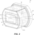
- FIG. 2 further illustrates the hermetically sealed optical sub-assembly 200 according to one implementation of the invention.
- the sub-assembly 200 provides an air-tight sealed enclosure for placement of a TEC 210 and sub-mounted lasers 215A-N.
- a spacer 220 is incorporated underneath the lasers 215A-N.
- This spacer 220 may comprise a material, such as ceramic, or other material intended to dissipate heat from the sub-mounted lasers 215A-N.
- the lasers 215AN may be individually sub-mounted (as discussed with regard to FIGS. 6A-E ) or alternatively mounted together on a sub-mount.
- one or more lenses may be mounted adjacent to the lasers 215A-N.
- Metalized pads 245 may be used to carry current to the sub-mounted lasers 215A-N.
- this gap is filled with electrical conductive adhesive (like silver filled epoxy), there is a risk of electrical shortage due to overflowing epoxy. Therefore, an epoxy that has high thermal conductivity but is not electrically conductive is preferred.
- an epoxy filled with ceramic particles can be used to provide a thermal, but not electrical, conductive epoxy (as discussed further with regard to FIG. 3 ).
- the temperature inside the hermetically sealed sub-assembly 200 may be measured by a temperature sensor like thermistor 240.
- the optical sub-assembly also comprises a window cap 230 that allows laser light to reach the modulator 110 optical signal inputs 120A-N (as shown in FIG. 1 ).
- an isolator 235 is located next to the sub-mounted lasers 215A-N. However, as described herein, this isolator 235 alternatively may be located outside the sub-assembly.
- FIG. 3 illustrates a cross section view of an optical communication device 100 according to an implementation of the invention.
- the TEC 210 and header 205 are turned 90-degrees to a substantially vertical position. Doing so allows for the height tolerances to be easily accounted for between the location of the modulator 110 and the output of the lasers 215A-N.
- the spacer 220, sub-mounted lasers 215A-N, and isolator 235 could be adjusted vertically to account for any variances arising between the placement of the modulator 110 and the lasers 215A-N.
- the sub-assembly 200 itself could be adjusted when placed in the optical platform 105 to create proper alignment between the lasers 215A-N and modulator 110, if required, before being fixably attached to the optical platform.
- a gap 310 is provided between the sub-mount of the laser (i.e., silicon) and the TEC 210 to prevent an electrical shortage at the laser.
- heat travels from the laser (i.e., the source of the heat), down through the sub-mount, and through the spacer 220 to the TEC 210.
- the gap 310 may be filled with a high thermal conductivity epoxy (e . g ., 3W/mK), such as epoxy filled with ceramic particles, to improve thermal performance, thus allowing the heat to travel directly through the epoxy to the TEC 210.
- a high thermal conductivity epoxy e . g ., 3W/mK
- An example illustrates the thermal efficiency gained through this approach.
- FIG. 4 illustrates a perspective view of an optical communication device according to another implementation of the invention.
- the isolator 235 in this implementation is shown outside of the hermetically assembled sub-assembly 200.
- this implementation illustrates that the optical communication device 100 may connect to an optical network through any number of interface 130 configurations ( e . g ., receptacles).
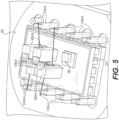
- individual sub-mounted lasers 505A-N may be placed on a TEC in an opposing configuration to accommodate a smaller pitch as previously discussed. This configuration may be used as an alternative to the multiple lasers on a sub-mount configuration.
- the sub-mounted lasers beneficially have lenses 510A-N to focus or collimate the laser light so that it may extend through the window cap 230 and reach the modulator inputs 120A-N.
- a lens array may be used in place of individual lenses.
- FIGS. 6A through 6E illustrate a preferred design and configuration for the placement of individual sub-mounted lasers 505A-N according to an implementation of the invention.
- a single sub-mounted laser is shown.
- the laser on individual sub-mount design comprises a laser 605 with a wire bond, burn in pads 610 (for electrical contact during burn in needle or pin contact), and a clearance 615 cut to avoid contact with the wire bond of adjacent lasers.
- the clearance 615 may be formed by a dicing blade without adding much cost to the manufacturing process.
- FIG. 6B further illustrates the placement of the single sub-mounted laser 505 on the TEC 210 according to an implementation of the invention.
- the laser on a sub-mount 505 may be glued or otherwise fixably attached to the TEC 210 and a wire bond may be extended to form an electrical connection to a pin on the header 205 or other pin assembly used in the hermetically sealed sub-assembly 200.
- a second sub-mounted laser 505 may be placed on the TEC 210 adjacent to and opposing the first individually sub-mounted laser 505. This configuration allows for efficient routing of wire bonds 625A-N to pins on the header 205. Further, as shown, this placement allows adequate clearance for using a tool 620 to attach the wire bonds 625A-N.
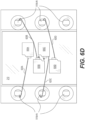
- FIG. 6D illustrates the placement of four sub-mounted lasers 505A-D on the TEC 210 according to an implementation of the invention. Each may be connected to respective pins 515A-N through wire bonds 625A-D.
- FIG. 6E illustrates the placement of four lenses on the four lasers 505A-N on individual sub-mounts on a TEC 210 according to a further implementation of the invention. As previously noted, a lens array could alternatively be used in place of the individual lenses.
- this pitch can range from 0.5mm to 1.0 mm, and a pitch of 0.5 mm is shown in FIGS. 6D through 6E .
- This pitch provides advantages because it allows for denser component arrangement, smaller footprint and lower cost.
- FIG. 7 an exemplary implementation of the sub-mounted laser 505A-N configuration is shown with a metal (or other material) frame 705 that has been optionally glued or otherwise fixably attached to the sub-mounted lasers 505A-N around the lenses 510A-N to stabilize the structure.
- a metal (or other material) frame 705 that has been optionally glued or otherwise fixably attached to the sub-mounted lasers 505A-N around the lenses 510A-N to stabilize the structure.
- Such stabilization allows for more stable performance over all operations, conditions and in better reliability.
- FIGS. 8A through 8B illustrate views of another optical communication device according to an implementation of the invention.
- the optical communication device 100 comprises an optical bench/platform 805 and a hermetically sealed optical sub-assembly 800 similar to that shown in FIG. 1 .
- the optical sub-assembly 800 design varies.
- the TEC 210 in sub-assembly 800 is positioned horizontal relative to the modulator 110.
- sub-mounted lasers 215A-N (which may be mounted together or individually sub-mounted) are positioned on the top of the TEC 210 to provide heat dispersion required for the lasers.
- the laser might not require a TEC 210 within the hermetically sealed sub-assembly 800, in which case the lasers would be height adjusted with a spacer as required to meet alignment with the window cap 815 positioned between the lasers 215A-N and the inputs 120A-N to the modulator 110.
- FIG. 8B when a TEC 210 is utilized, height adjustments of the TEC 210 in respect to platform 805 and/or the modulator 110 may be made by placing the components using a tooling component (shown by dashed line 840 in FIG. 8B ) and then welding the bottom lid 825 with the TEC 210 at the preferred height to metal ring 830 A-N.
- FIGS. 8A-B illustrate that a second hermetic seal between 830A-N and 810 can be used to join the top metal lid 810 to the platform 805 (which, in this implementation, is multi-layer ceramic but may be any suitable material).
- FIG. 8B illustrate that a second hermetic seal between 830A-N and 810 can be used to join the top metal lid 810 to the platform 805 (which, in this implementation, is multi-layer ceramic but may be any suitable material).
- FIG. 8B illustrate that a second hermetic seal between 830A-N and 810 can be used to join the top metal lid 810 to the platform 805
- the modulator 110 and integrated circuit board 115 may be pre-adjusted height-wise by the use of a spacer 820, which may be machined as a part of the platform 805 or added afterwards during the manufacturing process.
- the brazed metal rings 830 A-N used in welding should comprise ceramic with inferior RF performance. Therefore, the RF routing should go directly to the PCB as opposed to being routed via the ceramic. This may be done with wire bonds.
- the isolator 235 is shown inside the hermetically sealed sub-assembly 800, it may alternatively be located outside the hermetic enclosure 800 as discussed previously (if required at all).
- the inventive optical communication device 100 may be manufactured without the use of a standard TO-header, although it is economically preferable to use a TO header instead of hermetic ceramic feed-through package.
- a continuous light may be fired from the lasers 21 5A-N. While firing, the lasers 215A-N are cooled by TEC 210. The laser light is passed through lenses to collimate the light adjacent to the lasers and then focused outside the hermetically sealed optical sub-assembly 800, where they are coupled to the optical modulator 110. As previously discussed, an isolator 235 may be situated inside or outside the hermetically sealed assembly 800. The modulator 110 then modulates the laser light based on input from the PCB 115 and outputs the modulated signal to the optical network 130.
- FIGS. 9A through 9B illustrate yet additional views of an optical communication device 100 according to another implementation of the invention.
- height tolerances may be adjusted in the optical sub-assembly 900 by adjusting distance/height between modulator 110 and spacer 820.
- the modulator 110 silicon photonic chip
- the carrier material could be weldable kovar ® metal.
- a spacer 820 may also be used to adjust other height adjustments on the modulator 110 side; various shims in stepped-height tolerance variations could be used between the output of the sub-assembly 900 and the input(s) 120A-N to the modulator 110. (Similarly, height adjustments (instead of modulator height adjustments) could likewise be done inside hermetic area 810 between laser sub-mount 215A-N and TEC 210 (not shown)). In either case as before, a window cap 815 is employed to allow communication between the hermetically sealed lasers 815A-N and the modulator 110 (which in turn may send signals to an optical network through optical interface 130).
- FIG. 10 illustrates a subassembly consisting of carrier 1015, 1010 and 1005.
- a singulated sub-assembly is shown, but it could be part of a wafer scale assembly ( i.e., a wafer of many carriers 1015).
- Carrier 1015 has pre-defined breaks 1020A-B according to an implementation of the manufacture of the invention. Such breaks 1020A-B ensure easy separation of modulator 1010 and laser section 1005 in subsequent process steps.
- Wafer scale assembly can have cost and handling advantages.
- An additional advantage is pairing up of specific laser sub-mounts and modulators. The pairing can be kept throughout the whole process resulting in easier optical alignment process and better final optical coupling.
- the modulator 1010 and laser sub-mount 1005 can be aligned approximately adjacent to the breaks as shown.
- the complete subassembly 1000 can then be attached to the optical bench and header simultaneously and separated afterwards using pre-defined break lines 1020A-B. This manufacturing process allows sealing of the laser sub-mount portion without having the modulator in close proximity and in limited tooling access (as shown in FIGS. 13B-E ).
- FIG. 11 illustrates a subassembly 1100 with pre-defined breaks 1115A-B according to another implementation of the manufacture of the invention. Similar to the implementation shown in FIG. 10 , the breaks 1115A-B allow for separation of laser portion 1105 and modulator portion 1110 in subsequent process steps. However, in this implementation, a larger single silicon chip 1100 encompasses both portions, eliminating the need for additional carrier 1015,
- a subassembly 1015 with pre-defined breaks 1020A-B may be aligned using a tool 1205.
- the two sub-mounts in a first, course alignment step are placed approximately aligned with the pre-defined breaks 1020A-B.
- Proper height alignment between the sub-mounts is guaranteed by bond line control between subassembly 1015 and modulator sub-mount 1010 and between subassembly 1015 and laser sub-mount 1005.
- a jaw tool 1205 may be inserted into the space between the sub-mounts and opened as shown in FIG. 12B to position the two individual sub-mounts.
- the jaw tool references off of the precision etched features on sub-mounts 1005 and 1010). As shown, this may be performed after laser attach and burn in for laser sub-mount 1005 but before the final placement of specific components such as the isolator the modulator and laser lenses. However, such tooling could be performed at any time prior to final attachment of the sub-mounts.
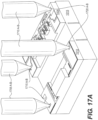
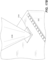
- FIGS. 17A through 17B illustrate another method of aligning the laser sub-mount section 1005 and modulator section 1010.
- a first tool 1705A-B may be inserted into slots 1715A-B manufactured into the sub-mount section 1005 and modulator section 1010, thus providing angular alignment.
- a second tool 1710A-B may be inserted into inverted pyramids 1720A-B.
- the combination of the second tool 1710A-B which preferably comprises two elongated columns ( e . g ., conical pins in a collet used to hold the component), each ending in a pyramid or pointed shape, allows for proper lateral alignment when placed into the inverted pyramids 1720A-B. This is shown in detail in FIG. 17B , as second tool 1710A is pressed into the inverted pyramid slot 1720A that is machined or chemically etched into the modulator section 1010.
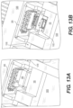
- FIGS. 13A through 13E illustrate further tooling of an optical communication device 100 according to an implementation of the manufacture of the invention.
- a pre-formed tool 1305 holds the optical platform 105 in place against a header 205 (that is stationary during the tooling process).
- a second tool 1310 provides proper course alignment for placing the sub-mount or carrier wafer.
- a subassembly 1100 with pre-formed breaks (as discussed above with reference to FIG. 11 ) - or alternatively a wafer 1015 pre-formed with breaks (as discussed above with reference to FIG. 10 ) - is positioned on top of the space next to the thermo-cooler 210 and on top of the optical platform 105.
- epoxy may be used to secure the sub-mount 1100 to the spacer 220 and optical platform 105. Curing can be performed in the fixture.
- the portion of the subassembly 1100 between the breaks is broken ( i.e., cracked) under controlled conditions. This may be performed by a controlled tooling split or controlled stress exposure to a weak area of the sub-mount. Whatever the case, the middle portion of the sub-mount 1100 (or wafer, if using a wafer configuration) can be removed or will fall away, as shown in FIG. 13C .
- the tooling members 1310, 1305 have been removed, along with the optical platform 105, thus leaving the header 205 stabilized in the fixture with the TEC 210, laser sub-mount 1105, and spacer 220. With this increased access, a thermistor 1320 may be added for heat monitoring and wire bonding may occur.
- a hermetic sealing step (either projection weld or laser seam sealing) will secure the front cover 225 of the optical sub-assembly 200 to the header 205.
- Tooling member 1305 and tooling member 1315 may be used during this step.
- the optical sub-assembly comprises a window cap 230 for sending laser light/signals.
- the enclosure of the sub-assembly 200 can be hermetically sealed by soldering or welding around the joint between the front cover 225 and the TO-header 205. After sealing 225 to 205, tooling 1305, 1310 and 1300 are joined together again.
- splitting and re-joining of tooling 1305, 1310 and 1300 can be done repeatedly and precisely if designed right such that optical coupling between laser sub-mount 1005 and modulator sub-mount 1010 is maintained without additional active re-alignment.
- optical bench 105 and header 205 can be joined at interface 1350A and 1350B to secure alignment permanently (attach methods could be soldering, laser welding or adhesive attach).
- the optical communication device 100 can then be removed from the clasp and additional parts (such as a PCB board and optical connector) can be added as required.
- one way of joining header 205 to optical bench 105 is to rely on tooling maintaining the optical alignment between laser sub-mount 1005 and modulator sub-mount 1010. This could be advantageous during manufacturing because it is faster and less expensive due to the avoidance of additional alignment steps. However, because optical coupling could be compromised, there could be applications where this is acceptable, while other applications are less forgiving and require highest possible coupling. In those cases, after sealing of front cover 225 to header 205, an additional active multiple access alignment step could be required between header 205 and optical bench 105 before both parts are joined at interface 1350A and 1350B.
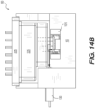
- an input lens array 1410 could be used in combination with an angled reflector 1405 to direct the optical signals into the modulator 1010.
- the input array 1410 receives laser light (here shown as receiving four laser beams shown as dashed lines) from the laser sub-mount.
- the modulator 1010 would then modulate the light (by encoding data and multiplexing) the laser inputs and would in turn send a single light beam to the optical network.
- the laser output lens (or lenses) 125 for the modulator 110 may be placed proximate to the optical connector 130.
- FIG. 1 the laser output lens (or lenses) 125 for the modulator 110 may be placed proximate to the optical connector 130.
- this may also be done by using an angled reflector that bends the light 90 degrees and directs it to the optical interface/receptacle 130 that interfaces with the optical network.
- an angled reflector that bends the light 90 degrees and directs it to the optical interface/receptacle 130 that interfaces with the optical network.
- various implementations are envisioned for processing laser signals once coupled to the modulator 110, and the specific steps of processing performed by a photonic modulator 110 are not mandated by this disclosure.
- the inventive optical communication device 100 is not limited to any specific type or method of optical processing.
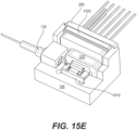
- FIGS. 15A-E illustrate yet another tooling of an optical communication device 1 00 according to an implementation of the manufacture of the invention.
- a pre-formed tool 1505 holds the optical platform 105 in place against a header 205 (that is stationary during the tooling process).
- a second tool 1515 provides proper course alignment for placing the sub-mount or carrier wafer.
- a wafer 1000 with pre-formed breaks (as discussed above with reference to FIG. 10 ) - or alternatively a silicon chip with pre-formed breaks (as discussed above with reference to FIG. 11 ) - is positioned on top of the space next to the thermo-cooler 210 and on top of the optical platform 105.
- the optical platform 105 has a pre-formed area to insert a modulator 1000 for proper alignment.
- epoxy may be used to secure the wafer 1100 (with sub-mount portions) to the TEC 210 and optical platform 105. Curing can be performed in the fixture.
- the portion of the wafer 1000 between the pre-formed breaks is cracked under controlled conditions. This may be performed by a controlled tooling split or controlled stress exposure to a weak area of the sub-mount. Whatever the case, the middle portion of the wafer 1000 (or chip, if using a silicon sub-mount configuration) can be removed or will fall away, as shown in FIG. 15C .
- the tooling members 1510 and 1515 are then removed, along with the optical platform 105. leaving the header 205 stabilized in the fixture with the TEC 210 and laser sub-mount portion 1005. With this increased access, a thermistor may be added for heat monitoring and wire bonding may occur.
- a hermetic sealing step (either projection or weld or laser seam sealing) will secure the front cover 225 of the optical sub-assembly 200 to the header 205 as shown to the right in FIG. 15C .
- Tooling member 1510 and tooling member 1515 may then be re-inserted as shown in FIG. 15D .
- splitting and re-joining of tooling members 1505, 1510 and 1515 can be done repeatedly and precisely if designed right such that optical coupling between sub-mount portions 1005 and 1010 is maintained without additional active re-alignment.
- the optical sub-assembly comprises a window cap 230 for sending laser light/signals.
- the enclosure of the sub-assembly 200 can be hermetically sealed by soldering or welding around the joint between the front cover 225 and the TO-header 205. After sealing cover 225 to header 205, tooling members 1505 and 1510 and 1515 are joined together again. Finally optical bench 105 and header 205 can be joined at their interfaces to secure alignment permanently (attach methods could be soldering, laser welding or adhesive attach).
- the optical communication device 100 can then be removed from the clasp and additional parts (such as a PCB board and optical connector) can be added as required as shown in FIG. 15E .
- FIG. 16A illustrates yet another example of the optical communication device 100 according to another implementation of the invention.
- a window cap 230 is again used to transmit laser light from inside the hermetically enclosed sub-assembly 200.
- a lid 1605 may be used to seal the sub-mounted lasers after they are inserted in the cover 225 during the manufacturing process.
- Electrical leads 1625A-N e . g ., made from low cost hermetic glass/metal seal
- a modulator portion 1010 may then be positioned on an optical bench 105 outside of the sub-assembly 200 to receive the laser light through the window cap 230. As described previously, the modulator portion 1010 may then modulate signals using the light and utilize an interface (not shown) to access an optical network.
- the TEC 210 is horizontal in this implementation, allowing height adjustments to be performed as previously noted with reference to FIGS. 8 through 9 .
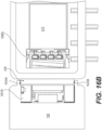
- optical bench 105 can be height adjusted by moving 105 up or down with reference to the optical sub-assembly 200 and, in particular, the window cap 230, which are stationary. Once the right height is found, optical bench/platform 105 can be permanently attached to the hermetically sealed sub-assembly 200 and window cap 230 with laser welding as indicated with arrows in FIG. 16B .
- individual lasers 120A-N can be aligned, as a last step, to the modulator 110 rather than using a lens array 1610 like the one shown in FIG. 16A . That way optical misalignment of the multiple collimated beams to each other can be compensated and maximum coupling can be achieved.
- the more efficient lens array 1610 could be used instead.
- an optical flat may be used in the optical subassembly. This may be beneficial since the window in the window cap may not be perfectly aligned 90-degrees, but may have some random distribution in the range of +/- 2 degrees. Such a situation introduces beam walk (vertically to optical beam) in the range of 6 to 7 ⁇ m. Accordingly, adding an optical flat and tilting it in an opposite way to the random tilt of the window may be used to beneficially recover the coupling loss due to beam walk.
- a flat window of thickness "h" can be inserted into the collimated beam between the TO and waveguide and the flat window can be tilted and secured to shift the beam by distance "d".
- a secondary recovery mode could be used to recover optical tilt introduced by uncontrolled shift during the sub-assembly to platform attachment.
- a single/double wedge/prism could be used to recover loss and bend the collimated beam back to center (similar to that described with reference to the lens array 1610).
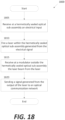
- FIG. 18 illustrates an example method 1800 of using an efficient optical device.
- a hermetically sealed optical sub-assembly receives an electrical input. This input may be generated from an outside source or a source residing at the sub-assembly.
- one or more lasers are fired within the hermetically sealed optical sub-assembly. As noted herein, this laser or lasers reside on a sub-mount and are affixed to a thermo-cooler.
- the laser beam generated from the laser is then received outside the hermetically sealed sub-assembly at a modulator.
- the modulator may or may not act on the beam to generate a signal for use in an optical communication network. In either case, however, at step 1820 the beam is directed through the modulator and output to an optical communication network.
- any number and type of optical connectors may provide access for the device to communicate with the optical network.
- Figure 19 provides an example method of manufacturing an optical communication device according to one implementation of the invention.
- a laser sub-mount is positioned on a carrier wafer adjacent to a first pre-defined break in a carrier wafer.
- pre-defined breaks may be instead made in a single sub-mount that can carry both a laser portion and a modulator portion in lieu of using a carrier wafer.
- a modulator sub-mount is then positioned adjacent to a second pre-defined break in the carrier wafer.
- the sub-mounts may be glued or otherwise fixably attached to the carrier wafer. Further, to ensure proper alignment before or after adhesion material is applied, a jaw tool or inverted pyramid tool (as disclosed herein) may be used to align the two sub-mounts.
- the laser-sub-mount (via the carrier wafer or in addition to the carrier wafer) is secured to a thermo-electrical cooler at step 1915.
- the modulator sub-mount (via the carrier wafer or in addition to the carrier wafer) may be secured to an optical platform to hold the sub-assembly and modulator components in place.
- the portion of the carrier wafer between the two sub-mounts may be broken or cut away and removed at step 1925.
- the modulator section may optionally then be removed to allow tooling access to the thermo-electrical cooler and laser sub-mount.
- the laser sub-mount and at least a portion of the thermo-electrical cooler is sealed inside a hermetically sealed sub-assembly that contains a window for communicating between the laser sub-mount and modulator sub-mount.
- the window allows a laser beam to be fired from a laser on the hermetically sealed sub-mount and received by an input on the modulator that is not hermetically scaled.
- any of the alignment techniques disclosed herein may be used.
Landscapes
- Physics & Mathematics (AREA)
- Optics & Photonics (AREA)
- General Physics & Mathematics (AREA)
- Electromagnetism (AREA)
- Condensed Matter Physics & Semiconductors (AREA)
- Engineering & Computer Science (AREA)
- Computer Networks & Wireless Communication (AREA)
- Signal Processing (AREA)
- Manufacturing & Machinery (AREA)
- Microelectronics & Electronic Packaging (AREA)
- Semiconductor Lasers (AREA)
- Optical Modulation, Optical Deflection, Nonlinear Optics, Optical Demodulation, Optical Logic Elements (AREA)
- Optical Communication System (AREA)
Description
- The present disclosure relates generally to methods and systems for communicating over an optical communication network.
- Next generation optical solutions utilize silicon photonics in order to achieve power control and continued miniaturization. Using silicon photonic optical modulators within transmitting optical sub-assemblies (TOSAs) for high speed data communication with greater than 40 gigabyte (Gb) transmission rates, one typically needs a continuous light source in the form of semiconductor lasers to be aligned to the modulator section where light is coupled from the laser to the modulator input with the help of individual lenses or lens arrays (to minimize alignment effort). Typically, the lens(es) and modulator are then hermetically sealed inside a suitable enclosure to cool the components without forming condensation. While the creation of such optical devices provides increased throughput and miniaturized structures, the energy requirements for these devices, however, remains high due to the electrical energy required to cool the laser and other components (e.g., modulator) hermetically sealed within the enclosure. Further, manufacturing requirements for perfecting height tolerances in the proper alignment of the lasers within the hermetically sealed enclosure remain strict, and in some cases manufacturing is prohibited or slowed due to these requirements.
- Accordingly, a solution is needed for an optical device with increased energy efficiency that also can retain high throughput characteristics. Additionally, a solution is needed for an efficient optical communication device with high throughput that may be manufactured using lower cost components. Additionally, a solution is needed for a method of manufacturing an optical communication device that can be performed more easily yet still maintain the strict tolerances required for such devices.
US2004/0076384 relates to an optical module. According to the abstract of this document the optical module includes an optical component, a body incorporating an optical element, and a metallic sleeve having a tubular shape. The optical component includes a nonmetallic ferrule having an optical fiber insertion hole, and a metallic holder which covers part of the ferrule. In this optical module, part of the holder is inserted into the sleeve, and is positioned and welded to the sleeve. The sleeve is positioned to a tubular portion of the body and welded thereto.
US2005/0129374 relates to a modular optoelectronic package. According to the abstract of this document each functional piece for a particular optoelectronic product may be packaged individually. Each package may be equipped with one or more optical windows through which collimated beams are allowed to pass. The individual packages or modules may be mated and aligned together in such a way that the output-collimated beam of one package becomes the input-collimated beam of a second package. In this fashion, any number of individual packages may be linked together to form an optical device performing a more complex operation.
WO99/42879
EP0467359 relates to a laser diode assembly. According to the abstract of this document the laser diode assembly is capable of controlling a temperature of a laser diode chip with a high accuracy. A Peltier device is mounted on a base member, and a carrier is mounted on the Peltier device. On the carrier are mounted the laser diode chip, a thermistor, and a relay block. A terminal for connecting the thermistor to an external circuit is provided so as to extend through the base member.
The thermistor and the relay block are connected together by wire bonding, and the relay block and the terminal are also connected together by wire bonding. The laser diode assembly further includes a control circuit for controlling a driving current for the Peltier device contacting with the carrier so as to maintain a resistance of the thermistor fixed on the carrier at a constant value. - The components in the drawings are not necessarily to scale relative to each other. Like reference numerals designate corresponding parts throughout the several views.
-
FIG. 1 illustrates a perspective view of an optical communication device according to an implementation of the invention; -
FIG. 2 illustrates a hermetically scaled laser sub-assembly showing a single sub-mount with multiple lasers on it according to an implementation of the invention; -
FIG, 3 illustrates a cross-section view of an optical communication device according to an implementation of the invention; -
FIG. 4 illustrates a perspective view of an optical communication device according to an implementation of the invention; -
FIG. 5 illustrates placement of individual sub-mounted lasers on a TEC according to an implementation of the invention; -
FIG. 6A illustrates an individually sub-mounted laser according to an implementation of the invention; -
FIG. 6B illustrates the placement of a single laser on a sub-mount on a TEC according to an implementation of the invention; -
FIG. 6C illustrates the placement of two lasers on individual sub-mounts on a TEC and illustrating routing of wire bonds including clearance check for wire bond capillary according to an implementation of the invention; -
FIG. 6D illustrates the placement of four lasers on individual sub-mounts on a TEC according to an implementation of the invention; -
FIG. 6E illustrates the placement of four lenses and wire leads on four individually sub-mounted lasers on a TEC according to an implementation of the invention; -
FIG. 7 illustrates a perspective view of the alignment of four lenses on four lasers on individual sub-mounts on a TEC providing mechanical stabilization and improved reliability according to an implementation of the invention; -
FIG. 8A illustrates a perspective view of an optical communication device with horizontal TEC mounting according to an implementation of the invention; -
FIG. 8B illustrates a side view of the alignment of an optical communication device according to an implementation of the invention; -
FIG. 9A illustrates a perspective view of an optical communication device according to an implementation of the invention; -
FIG. 9B illustrates a side view of the alignment of an optical communication device according to an implementation of the invention: -
FIG. 10 illustrates a wafer configuration with pre-defined breaks according to an implementation of the manufacture of the invention; -
FIG. 11 illustrates a silicon photonics chip (e.g., sub-mount) with pre-defined breaks according to an implementation of the manufacture of the invention; -
FIG. 12A illustrates a silicon photonics chip and laser sub-mount mounted to a carrier wafer configuration with pre-defined breaks according to an implementation of the manufacture of the invention; -
FIG. 12B illustrates the tooling of a wafer configuration with pre-defined breaks according to an implementation of the manufacture of the invention; -
FIGS. 13A-E illustrate the tooling of an optical communication device according to an implementation of the manufacture of the invention; -
FIGS. 14A-B illustrate the flow of signals in an optical communication device according to an implementation of the invention; -
FIGS. 15A-E illustrate the tooling of an optical communication device according to another implementation of the manufacture of the invention; -
FIG. 16A illustrates a perspective view of an optical communication device according to another implementation of the invention; -
FIG. 16B illustrates a top view of an optical communication device according to another implementation of the invention; -
FIG. 16C illustrates a cross-section view of an optical communication device according to another implementation of the invention; -
FIGS. 17A-B illustrate a silicon photonics chip and laser sub-mount mounted to a carrier wafer configuration with pre-defined breaks according to another implementation of the manufacture of the invention; -
FIG. 18 illustrates a method of using an efficient optical communication device according to one implementation of the invention; and -
FIG. 19 illustrates a method of manufacturing an optical communication device according to one implementation of the invention. - Aspects of the invention are set out in the independent claims and preferred features are set out in the dependent claims.
- There is also described herein an optical communication device comprising a laser within a hermetically sealed sub·-assembly for use in an optical communications network. A thermo-electrical cooler may also reside within the hermetically sealed sub-assembly for dissipating heat generated by the laser. A window may form part of the hermetically sealed sub-assembly for communicating a light beam between the laser and an optical input situated outside the hermetically sealed sub-assembly. The optical input may be connected to an optical modulator outside the hermetically sealed sub-assembly to modulate the light beam and send a modulated optical signal to an optical communication network.
- As also described herein, a laser may receive at a hermetically sealed optical sub-assembly an electrical input from an external source. In response, a laser on a sub-mount within the hermetically sealed optical sub-assembly may be fired corresponding to the electrical input. An optical modulator outside of the hermetically sealed sub-assembly may receive the output of the first laser and modulate the light and send the modulated light to an optical communication network through an optical connector that forms part of the optical communication device.
- Further exemplary implementations disclosed herein include methods of manufacturing an optical communication device and hermetically sealed sub-assembly. In one example implementation, a method of manufacturing an optical communication device may include positioning a first sub-mount configured to accommodate an optical laser on a carrier wafer approximately adjacent to a first pre-defined break line in the carrier wafer. A second sub- mount is then configured to accommodate an optical modulator on the same carrier wafer approximately adjacent to a second pre-defined break line in the carrier wafer. Optionally, a jaw tool or inverted pyramid tool may then be used to align the first and second sub- mounts such that lasers/lenses on the first sub-mount and the modulator on the second sub-mount are coarsely pre- aligned with subsequent fine alignment step for lenses to maximize optical coupling between laser and modulator.
- The first sub-mount can further be hermetically sealed in a sub-assembly. A window in the sub-assembly is aligned with the output of the optical laser. The optical device platform and sub-assembly may then be placed adjacent to each other such that the first and second sub-mounts are optionally passively realigned, thus allowing the laser(s) within the first sub-assembly to be aligned with the input(s) of the optical modulator.
- There is also described herein, a method of manufacturing an optical communication device entailing preparing a first pre-defined break line in a submount approximate to a portion of the sub-mount that is configured to accommodate an optical laser and preparing a second pre-defined break line in the sub-mount approximate to a portion of the sub-mount that is configured to accommodate an optical modulator, The sub-mount may then be attached perpendicular to a TEC and parallel to an optical device platform (i.e., optical bench). The portion of the sub-mount between the first and second break lines may then be removed so as to allow further manufacture in accordance with methods disclosed herein.
- In some optical network devices, lasers are used that require temperature control with a thermo-electrical cooler (TEC) to maintain output wavelength and/or power. To avoid condensation on temperature controlled (cooled) areas, a hermetic enclosure is utilized to enclose the electrical components, modulators, and lasers. For example, in optical device applications, a transmitter optical sub-assembly (TOSA) may be created by hermetically sealing components inside a suitable enclosure. In this way the components (which typically include lasers and optical modulators) may be cooled without forming problematic condensation within the optical device. Accordingly, the TOSA may take electrical input signals through connection leads and export the optical signals through an optical receptacle (e.g., an optical connector or patch cord is inserted into a receptacle to guide light via fiber to its final destination) by way of the hermetically sealed laser and modulator assembly enclosure.
- While the creation of such an optical device provides increased throughput and miniaturized structures, the energy requirements for these devices remains high due to the electrical energy required to cool the laser and other components (e.g., modulator) hermetically sealed within the enclosure. This is in part at least because all of the components are located on the TEC and multiple short wire bonds leading to the modulator increase power consumption.
- Further, because the modulator is within the hermetically enclosed structure, the electrical leads including multiple RF lines must be routed through non-conducting insulation (e.g., ceramic) from the inside of the enclosure to the connector portion while maintaining the hermeticity of the package, thus creating additional manufacturing expense and difficulty. Additionally, the final design of the connector remains high, as hermetic RF feed through is more costly compared to low cost DC feed-through (e.g., glass or metal). Furthermore, manufacturing requirements for perfecting height tolerances in the proper alignment of the lasers within the hermetically sealed enclosure remain strict, and in some cases manufacturing is prohibited or slowed due to these requirements.
- In an example implementation, the optical communication device disclosed herein may have a hermetic sub-assembly of lasers and thermo-electrical coolers (TEC) integrated within a sturdy optical platform or bench which further holds optical components - e.g., isolator, optical modulator, mirrors, connectors, and electrical chips/circuits. The cost of the inventive device may be reduced over conventional designs by using TO-industry parts without compromising performance and guaranteeing the highest yield possible. In various implementations disclosed herein, multiple lasers can be placed inside the hermetic package to allow multiple channel transmissions. A window cap on the hermetic enclosure may allow the unsealed components to receive and transmit information from/to the hermetically sealed laser components. In this way, less energy is consumed by the device than conventional optical device configurations.
- The present disclosure also provides methods for absorbing the large height tolerances of thermo-electrical coolers (TECs), which can be in the range of plus or minus 0.1 millimeters (mm), without compromising the stability of the optical package. Additionally, exemplary implementations disclosed herein allow for the burn-in of individual lasers to maximize yield and still allow for an arrangement of lasers on a certain pitch to be able to use lens arrays and couple light to a modulator with multiple inputs on the same pitch. The laser is on a silicon sub-mount.
- In further exemplary implementations disclosed herein, the inventive optical communication device has a window forming part of the hermetically sealed assembly for communicating between the laser and an optical input situated outside the hermetically sealed assembly. The optical input and/or inputs may be coupled to an optical modulator (comprising silicon photonics) through which signal processing may be performed on the signal from the laser. An isolator to direct the laser may be either outside or within the hermetically sealed assembly. The optical communication device may also have an optical output for communication with an optical communications network. Various types of optical connectors for receiving an optical signal from the optical output and accessing the optical communications network may also be used.
- The TEC that may be used in the optical communication device can be vertically or horizontally oriented within the hermetically sealed assembly. If vertically oriented, height tolerance adjustments of the laser may be made by adjusting the position of the laser vertically on the TEC. If horizontally oriented, height adjustments between the laser and the optical input may be made by varying the bottom lid of the hermetically sealed assembly or the depth of the optical modulator or depth of laser mounting. When the depth of the optical modulator or laser is varied, a spacer below the modulator or within the hermetically sealed enclosure below or above the TEC may be configured to account for height adjustments.
- Optionally, the optical communication device may have multiple lasers on a single sub-mount positioned on the TEC (instead of individual lasers on a sub-mount) such that a spacer is positioned underneath the sub-mount and adjacent to the TEC to facilitate heat dissipation generated from the laser or lasers.
- Exemplary implementations of the optical communication device described in the present disclosure thus provide for a reliable, flexible, and sturdy optical communication device. One implementation may have a transmitting optical sub-assembly for which low cost components from transistor outline industry (high volume) may be used, such as a standard transistor outline header (TO-header), and window cap with low cost glass/metal hermetic seal. Energy efficiency is provided by hermetically sealing limited areas, such as the cooled or uncooled laser(s) that may be used as continuous light sources. This allows for the optical modulator and connector sections of the inventive optical communication device to remain outside the hermetic package, providing advantages as described herein. This also prevents costly hermetic radio frequency (RF) feed through.
- According to the various implementations, the disclosure provided herein is capable of providing advantages over the conventional TOSA connector. First, the hermetic area disclosed herein may contain direct current (DC) lines and no radio frequency (RF) signals thus allowing cheaper and easier routing than conventional designs. (This is in part because glass/metal feed-through with round pins is only effective for less than 10-Gb speeds. Beyond 10-Gb speeds, ceramic multi-layer has superior RF performance (less reflection/radiation and more transmission of RF signals).) Specifically, preparing a feed-through of DC signals into the hermetic area is much cheaper and easier compared with routing RF signals because simple glass/metal seals can be used versus multiple ceramic layers mating with metal seals as required for RF routing. Second, the optical communication device may comprise, in certain implementations, lower cost standard packaging parts, such as ceramic sub-mounts, standard window caps, and/or standard pin headers. Third, the optical communication device may have a higher laser burn in yield due to the preferred individual laser on a sub-mount design described herein where individual sub-mounts may be replaced instead of replacing a multiple laser sub-mount due to a single laser failure. Fourth, the optical communication device may produce lower power consumption because it only requires that lasers within the hermetic package be cooled as opposed to electronics contained within the modulator section as required by conventional devices. Fifth, the optical communication device may produce a lower passive head load since no short wire bonds from hot to cold are required. Sixth, the optical communication device provides an elegant solution for the separation of lasers and modulator by tilting the TEC 90-degress (or substantially vertical) to deal with TEC height tolerances without compromising stability or requiring more complicated design features to absorb TEC height tolerances (like shimming, laser or modulator height adjustment).
- In one implementation disclosed herein, low-cost TO-header technology with multiple I/O pins can be used to allow DC routing of laser biases, along with TEC current and temperature sensor connections (e.g., connections for thermistor). The laser(s) can be mounted on individual sub-mounts. This would allow individual burn in of each laser on sub-mounts and passing dies could be used for subsequent assembly. That way burn in yield is maximized versus simultaneous burn in of several lasers on the same sub-mount which would make the whole sub-assembly fail if only one laser burn-in failed. However, it is to be understood by those of ordinary skill in the art, that the sub-assembly could use any kind of sub-mounts covering both individual or group (wafer) burn in strategies.
- If the preferred individual laser sub-mounts are implemented, the shape of the sub-mounts may allow for each individual laser to be mounted on the TEC top surface to allow light emission in line with the TO-package center axis. This would also allow multiple sub-mounts with lasers to be arranged on a pitch of as little as 0.5mm to match the pitch of the lens arrays and/or the modulator section pitch. To allow easy handling and burn in of individual sub-mounts, it is preferred that they have a minimum size of 0.8mm to 0.9mm. Also, burn in requires minimum pad size on laser sub-mounts to make a reliable electrical contact (e.g., with pogo pins). Optionally, the arrangement of several sub-mounts on the TEC top surface can be alternating (or opposing) so that all odd channels are facing one way and even channels are rotated the opposite way (i.e., 180 degrees). This allows the sub-assembly to maintain the desired smaller pitch (e.g., 0.5mm). Otherwise, a pitch such as 1.0 mm would be the minimum pitch size, accordingly limiting the packaging size. In accordance with the individual sub-mount implementation, a cut out on one sub-mount side may be utilized to avoid interference with the laser wire-bond of the adjacent channel. The clearance cut on the sub-mount can easily be added before sub-mount separation by a dicing blade without adding much cost. In contrast, conventional designs use more costly reactive ion etching on silicon to create clearance cuts.
- Electrical connection may be established by wire bonds from sub-mount pads to the TO-header pins (as discussed with reference to
FIG. 6 ). Layout of both sub-mount and header pins can also be carefully chosen to maintain a small footprint and still allow wire bondability. On the sub-mount backside where it makes contact with the TEC top surface, conductive epoxy can be used to electrically connect the sub-mount pad to a metalized or patterned TEC top surface and/or additional patterned substrate mounted to the TEC top surface (i.e., could be a common ground for all lasers). The electrical connection can be a 90-degree bend via the conductive epoxy on the sub-mount pad close to back side to TEC top surface. This would be the lowest cost solution (without a 90-degree epoxy path, wire bonds would need to replace the connection because there is limited space/access for additional pads; wrapping metal pads around edges opens up additional space to place pads but increases the cost for the sub-mount). Alternatively, as noted, sub-mounts with conductive paths wrapping around (multiple) edges could be used to have a wire-bond connection only. However, this would increase the cost of the sub-mounts. - Optionally, to increase the mechanical integrity of the laser sub-mount array on a vertically mounted thermo-electrical top surface a frame structure can be glued to the front side of the sub-mounts connecting all sub-mounts with each other and increasing the stiffness of the assembly.
- Each laser can be mounted at a controlled distance to the front face of the sub-mount. A first lens can then be aligned and glued to each of the front faces of the sub-mounts to collimate or bend the laser light. This allows larger physical separation between the laser and the modulator section to accommodate the hermetic sealing with a window cap. Alternatively a lens array can be aligned and glued to the laser sub-mount front surfaces.
- Accordingly, the hermetic sub-assembly comprised of a TO-header and window (lens cap) containing multiple lasers, TEC and temperature sensor (e.g., thermistor) builds a robust unit that can be easily handled and tested before being used in subsequent assembly steps. The optical sub-assembly can then be aligned and fixed (by weld, glue and/or solder) within the optical bench so that the laser signal/light may be horizontal to the optical bench. This requires a 90 degree tilt of the header with regards to the optical platform/bench. In this way, the optical setup is immune against any TEC height tolerances. It also allows exact alignment of laser beams in x/y/z and angle to match the optical height and position of the modulator such that the modulator height does not have to be strictly controlled.
- Consistent with this disclosure, the optical bench material may be a variety of materials, including but not limited to, kovar or CuW to match the silicon coefficient of thermal expansion (CTE) and to also provide good heat sinking in case of CuW. Metal injection molding (MIM) can alternatively be used for the optical bench in order to reduce cost for higher volumes of the optical communication device. Typical metal injection molding dimensional tolerances are acceptable for the present invention.
- Alternatively, ceramic could also be used as optical bench material but it is more challenging to machine to the required shape. Additionally, a hybrid of ccramic/metal or metal/metal is an option if laser welding is required, especially for a connection between the TO-header and the optical bench and the fiber optic connector/receptacle to the optical bench.
- According to one implementation of the manufacture of the inventive optical communication device, isolators between the lasers and modulator would be attached to the device, followed by the placement and adhesive attachment of the modulator to the optical bench. Coarse alignment is also acceptable in the event a secondary lens (or array) is used on the modulator input side (such a secondary lens alignment would require high precision). Alternatively, a staggered layout of modulator input channels would allow larger secondary lenses and easier tooling access. Further, in another alternative implementation, all modulator inputs can be on the same line and a secondary lens array could be used.
- To route the modulator output light more easily to a fiber (array) connector, it is beneficial to have the modulator output side be different than the input side to allow for an easier arrangement of components not available due to space constraints when arranging on the same side. In any event, the fiber (array) connector placement and attachment to the optical platform/bench can be either the last or second-to-last optical alignment step depending on process preferences for manufacturing the optical communication device. As noted, individual or array lenses can be used.
- As further disclosed herein, the optical bench can be designed such that one or more driver integrated circuits can be mounted adjacent to the modulator or even placed directly on the modulator. Connection to a printed circuit board (PCB) can be such that wire bonds or flex connections used between an integrated circuit and PCB or alternatively a cut out on the optical bench could allow a ball grid array (BGA) attachment of the integrated circuits to the PCB.
- A further aspect of an exemplary implementation of the optical communication device disclosed herein includes the heat sinking of the TEC. In a vertical orientation, the heat has to take a 90 degree turn from header backside to the heat sink which is typically parallel to the optical bench. By using high thermal conductivity steel for the header and an appropriate heat sink, which makes contact to the header back side (e.g., copper finger), the temperature drop within the heat sink path can be minimized to an acceptable level (e.g., adding an additional high thermal conductivity material to the header backside offers the heat a parallel path decreasing thermal resistance and temperature drop to ambient temperature).
- The figures disclosed herein provide further details for the inventive optical communication device.
-
FIG. 1 illustrates a perspective view of anoptical communication device 100 according to an implementation of the invention. Theoptical communication device 100 may comprise two main components: the optical platform/bench 105 and the hermetically sealedoptical sub-assembly 200. As shown, a modulator 110 (comprising silicon photonics) and a printed circuit board (PCB) 115 may be fixably attached to the opticalcommunication device platform 105. Additionally, an electrical integrated circuit 111 (e.g., a flip chip bonded via a BGA) may be bonded to themodulator 110. - One or
more input lenses 120A-N may reside on themodulator 110 to couple laser signals received from theoptical sub-assembly 200 into thephotonic modulator 110 for processing. Alaser output lens 125 on themodulator 110 may also be used to couple the output of thephotonic modulator 110 to an optical communication network through an optical interface 130 (such as thelensed fiber receptacle 130 shown inFIG. 1 or alternative receptacles (not shown)). It should be noted that additional components may be placed on the optical bench/platform 105, including but not limited to passive electrical components and active driver integrated circuits, mainelectrical PCB 115, and/or micro optics turning mirrors. The electrical connection to the PCB 115 (or other main electrical board) can be done by a ball grid array (BGA) or can also be done by flexible PCB or wire bond. - The
optical interface 130 may comprise a variety of forms, including but not limited to, a lensed fiber (shown inFIG. 1 ) or any other optical receptacle to allow a connection to an optical patch cord. Regardless of the type, theoptical interface 130 can be attached to the optical platform (e.g., glued, soldered or welded) before or after the output lens is aligned and put into place at the modulator output side to couple maximum light into theoptical interface 130. -
FIG. 2 further illustrates the hermetically sealedoptical sub-assembly 200 according to one implementation of the invention. The sub-assembly 200 provides an air-tight sealed enclosure for placement of aTEC 210 andsub-mounted lasers 215A-N. As shown, to maximize heat dissipation and increase mechanical stability, aspacer 220 is incorporated underneath thelasers 215A-N. Thisspacer 220 may comprise a material, such as ceramic, or other material intended to dissipate heat from thesub-mounted lasers 215A-N. The lasers 215AN may be individually sub-mounted (as discussed with regard toFIGS. 6A-E ) or alternatively mounted together on a sub-mount. To direct the optical light or signal from thelasers 215A-N to themodulator 110, one or more lenses (or a lens array) may be mounted adjacent to thelasers 215A-N. Metalized pads 245 may be used to carry current to thesub-mounted lasers 215A-N. As shown inFIG. 4 , there is agap 310 between theTEC 210 and the laser sub-mount (which is made of silicon) so that theelectrical pads 245 do not short on theTEC 210. If this gap is filled with electrical conductive adhesive (like silver filled epoxy), there is a risk of electrical shortage due to overflowing epoxy. Therefore, an epoxy that has high thermal conductivity but is not electrically conductive is preferred. For example, in one exemplary implementation, an epoxy filled with ceramic particles can be used to provide a thermal, but not electrical, conductive epoxy (as discussed further with regard toFIG. 3 ). - The temperature inside the hermetically sealed
sub-assembly 200 may be measured by a temperature sensor likethermistor 240. As further shown inFIG. 2 , the optical sub-assembly also comprises awindow cap 230 that allows laser light to reach themodulator 110optical signal inputs 120A-N (as shown inFIG. 1 ). In this implementation, anisolator 235 is located next to thesub-mounted lasers 215A-N. However, as described herein, thisisolator 235 alternatively may be located outside the sub-assembly. -
FIG. 3 illustrates a cross section view of anoptical communication device 100 according to an implementation of the invention. As shown in this implementation, theTEC 210 andheader 205 are turned 90-degrees to a substantially vertical position. Doing so allows for the height tolerances to be easily accounted for between the location of themodulator 110 and the output of thelasers 215A-N. For example, thespacer 220,sub-mounted lasers 215A-N, andisolator 235 could be adjusted vertically to account for any variances arising between the placement of themodulator 110 and thelasers 215A-N. Alternatively, the sub-assembly 200 itself could be adjusted when placed in theoptical platform 105 to create proper alignment between thelasers 215A-N andmodulator 110, if required, before being fixably attached to the optical platform. - As also shown in
FIG. 3 , agap 310 is provided between the sub-mount of the laser (i.e., silicon) and theTEC 210 to prevent an electrical shortage at the laser. In this configuration, heat travels from the laser (i.e., the source of the heat), down through the sub-mount, and through thespacer 220 to theTEC 210. Alternatively, as mentioned previously, thegap 310 may be filled with a high thermal conductivity epoxy (e.g., 3W/mK), such as epoxy filled with ceramic particles, to improve thermal performance, thus allowing the heat to travel directly through the epoxy to theTEC 210. An example illustrates the thermal efficiency gained through this approach. For example, with spacer thickness of t=0.5mm, the laser temperature may be reduced by approximately 1.2° C and for t = 2mm, the reduction can be approximately 0.5° C (assuming the temperature of the laser is 50° C and the ambient temperature is 75° C). This is significant, as with four lasers running at 120mA each, this amounts to a TEC power savings of 40mW per 1° C. -
FIG. 4 illustrates a perspective view of an optical communication device according to another implementation of the invention. As noted, theisolator 235 in this implementation is shown outside of the hermetically assembledsub-assembly 200. Further, this implementation illustrates that theoptical communication device 100 may connect to an optical network through any number ofinterface 130 configurations (e.g., receptacles). - In the implementation shown in
FIG. 5 . individualsub-mounted lasers 505A-N may be placed on a TEC in an opposing configuration to accommodate a smaller pitch as previously discussed. This configuration may be used as an alternative to the multiple lasers on a sub-mount configuration. In either case, to facilitate the exchange of laser light or signals between the sub-assembly 200 and themodulator inputs 120A-N, the sub-mounted lasers beneficially havelenses 510A-N to focus or collimate the laser light so that it may extend through thewindow cap 230 and reach themodulator inputs 120A-N. Alternatively, a lens array may be used in place of individual lenses. -
FIGS. 6A through 6E illustrate a preferred design and configuration for the placement of individualsub-mounted lasers 505A-N according to an implementation of the invention. InFIG. 6A , a single sub-mounted laser is shown. The laser on individual sub-mount design comprises alaser 605 with a wire bond, burn in pads 610 (for electrical contact during burn in needle or pin contact), and aclearance 615 cut to avoid contact with the wire bond of adjacent lasers. As noted previously, theclearance 615 may be formed by a dicing blade without adding much cost to the manufacturing process. -
FIG. 6B further illustrates the placement of the singlesub-mounted laser 505 on theTEC 210 according to an implementation of the invention. The laser on a sub-mount 505 may be glued or otherwise fixably attached to theTEC 210 and a wire bond may be extended to form an electrical connection to a pin on theheader 205 or other pin assembly used in the hermetically sealedsub-assembly 200. In accordance withFIG. 6C , a secondsub-mounted laser 505 may be placed on theTEC 210 adjacent to and opposing the first individuallysub-mounted laser 505. This configuration allows for efficient routing ofwire bonds 625A-N to pins on theheader 205. Further, as shown, this placement allows adequate clearance for using atool 620 to attach thewire bonds 625A-N. - As shown in
FIG. 6D , foursub-mounted lasers 505A-D have been placed on theTEC 210 according to an implementation of the invention. Each may be connected torespective pins 515A-N throughwire bonds 625A-D.FIG. 6E illustrates the placement of four lenses on the fourlasers 505A-N on individual sub-mounts on aTEC 210 according to a further implementation of the invention. As previously noted, a lens array could alternatively be used in place of the individual lenses. - The positioning of the
lasers 505A-N in a line in an opposing manner as shown inFIGS. 6B through 6E allows for a smaller controlled pitch. Preferably, this pitch can range from 0.5mm to 1.0 mm, and a pitch of 0.5 mm is shown inFIGS. 6D through 6E . This pitch provides advantages because it allows for denser component arrangement, smaller footprint and lower cost. - In
FIG. 7 , an exemplary implementation of thesub-mounted laser 505A-N configuration is shown with a metal (or other material)frame 705 that has been optionally glued or otherwise fixably attached to thesub-mounted lasers 505A-N around thelenses 510A-N to stabilize the structure. Such stabilization allows for more stable performance over all operations, conditions and in better reliability. -
FIGS. 8A through 8B illustrate views of another optical communication device according to an implementation of the invention. InFIG. 8A , theoptical communication device 100 comprises an optical bench/platform 805 and a hermetically sealedoptical sub-assembly 800 similar to that shown inFIG. 1 . However, inFIG. 8A , theoptical sub-assembly 800 design varies. Specifically, as shown in greater detail inFIG. 8B , theTEC 210 insub-assembly 800 is positioned horizontal relative to themodulator 110. Accordingly,sub-mounted lasers 215A-N (which may be mounted together or individually sub-mounted) are positioned on the top of theTEC 210 to provide heat dispersion required for the lasers. As noted previously, in some configurations the laser might not require aTEC 210 within the hermetically sealedsub-assembly 800, in which case the lasers would be height adjusted with a spacer as required to meet alignment with thewindow cap 815 positioned between thelasers 215A-N and theinputs 120A-N to themodulator 110. - As shown in
FIG. 8B , when aTEC 210 is utilized, height adjustments of theTEC 210 in respect toplatform 805 and/or themodulator 110 may be made by placing the components using a tooling component (shown by dashedline 840 inFIG. 8B ) and then welding thebottom lid 825 with theTEC 210 at the preferred height tometal ring 830 A-N. Additionally,FIGS. 8A-B illustrate that a second hermetic seal between 830A-N and 810 can be used to join thetop metal lid 810 to the platform 805 (which, in this implementation, is multi-layer ceramic but may be any suitable material). Optionally, as shown inFIG. 8B , themodulator 110 and integratedcircuit board 115 may be pre-adjusted height-wise by the use of aspacer 820, which may be machined as a part of theplatform 805 or added afterwards during the manufacturing process. Also the brazedmetal rings 830 A-N used in welding should comprise ceramic with inferior RF performance. Therefore, the RF routing should go directly to the PCB as opposed to being routed via the ceramic. This may be done with wire bonds. While theisolator 235 is shown inside the hermetically sealedsub-assembly 800, it may alternatively be located outside thehermetic enclosure 800 as discussed previously (if required at all). Further, as illustrated inFIGS. 8A-B , the inventiveoptical communication device 100 may be manufactured without the use of a standard TO-header, although it is economically preferable to use a TO header instead of hermetic ceramic feed-through package. - The operation of the
optical communication device 100 shown inFIGS. 8A and8B may be the same as that described previously. Specifically, a continuous light may be fired from the lasers 21 5A-N. While firing, thelasers 215A-N are cooled byTEC 210. The laser light is passed through lenses to collimate the light adjacent to the lasers and then focused outside the hermetically sealedoptical sub-assembly 800, where they are coupled to theoptical modulator 110. As previously discussed, anisolator 235 may be situated inside or outside the hermetically sealedassembly 800. Themodulator 110 then modulates the laser light based on input from thePCB 115 and outputs the modulated signal to theoptical network 130. -
FIGS. 9A through 9B illustrate yet additional views of anoptical communication device 100 according to another implementation of the invention. As shown inFIG. 9B , height tolerances may be adjusted in theoptical sub-assembly 900 by adjusting distance/height betweenmodulator 110 andspacer 820. With subsequent locking ofmodulator 110 to spacer 820 (e.g., via glue, welding, or solder), the modulator 110 (silicon photonic chip) could be sitting on an additional carrier (not shown) which is adjusted in respect tospacer 820. Especially for the locking method "welding," this is preferred since the carrier material could be weldable kovar® metal. Further, as with the implementation shown inFIGS. 8A-B , aspacer 820 may also be used to adjust other height adjustments on themodulator 110 side; various shims in stepped-height tolerance variations could be used between the output of the sub-assembly 900 and the input(s) 120A-N to themodulator 110. (Similarly, height adjustments (instead of modulator height adjustments) could likewise be done insidehermetic area 810 between laser sub-mount 215A-N and TEC 210 (not shown)). In either case as before, awindow cap 815 is employed to allow communication between the hermetically sealed lasers 815A-N and the modulator 110 (which in turn may send signals to an optical network through optical interface 130). - As discussed previously, the various implementations disclosed herein offer advantages over conventional designs. Such advantages include increased power performance (lower power consumption), more economical packaging designs, and potentially smaller device sizes. This list is not exclusive, but includes other advantages recognized by those of ordinary skill in the art.
- The present disclosure also provides an inventive method of manufacturing the inventive
optical communication device 100.FIG. 10 illustrates a subassembly consisting ofcarrier Carrier 1015 has pre-defined breaks 1020A-B according to an implementation of the manufacture of the invention. Such breaks 1020A-B ensure easy separation ofmodulator 1010 andlaser section 1005 in subsequent process steps. Wafer scale assembly can have cost and handling advantages. An additional advantage is pairing up of specific laser sub-mounts and modulators. The pairing can be kept throughout the whole process resulting in easier optical alignment process and better final optical coupling. For example, themodulator 1010 andlaser sub-mount 1005 can be aligned approximately adjacent to the breaks as shown. Thecomplete subassembly 1000 can then be attached to the optical bench and header simultaneously and separated afterwards using pre-defined break lines 1020A-B. This manufacturing process allows sealing of the laser sub-mount portion without having the modulator in close proximity and in limited tooling access (as shown inFIGS. 13B-E ). -
FIG. 11 illustrates asubassembly 1100 with pre-defined breaks 1115A-B according to another implementation of the manufacture of the invention. Similar to the implementation shown inFIG. 10 , the breaks 1115A-B allow for separation oflaser portion 1105 andmodulator portion 1110 in subsequent process steps. However, in this implementation, a largersingle silicon chip 1100 encompasses both portions, eliminating the need foradditional carrier 1015, - As shown in
FIGS. 12A through 12B , if two separate sub-mounts are used (e.g., alaser sub-mount 1005 and a modulator sub-mount 1010), asubassembly 1015 with pre-defined breaks 1020A-B according to an implementation of the manufacture of the invention may be aligned using atool 1205. InFIG. 12A the two sub-mounts in a first, course alignment step are placed approximately aligned with the pre-defined breaks 1020A-B. Proper height alignment between the sub-mounts is guaranteed by bond line control betweensubassembly 1015 and modulator sub-mount 1010 and betweensubassembly 1015 andlaser sub-mount 1005. However, to ensure proper side-to-side alignment, in one implementation ajaw tool 1205 may be inserted into the space between the sub-mounts and opened as shown inFIG. 12B to position the two individual sub-mounts. (The jaw tool references off of the precision etched features on sub-mounts 1005 and 1010). As shown, this may be performed after laser attach and burn in forlaser sub-mount 1005 but before the final placement of specific components such as the isolator the modulator and laser lenses. However, such tooling could be performed at any time prior to final attachment of the sub-mounts. - Similarly,
FIGS. 17A through 17B illustrate another method of aligning thelaser sub-mount section 1005 andmodulator section 1010. As shown, a first tool 1705A-B may be inserted into slots 1715A-B manufactured into thesub-mount section 1005 andmodulator section 1010, thus providing angular alignment. At the same time, asecond tool 1710A-B may be inserted into invertedpyramids 1720A-B. The combination of thesecond tool 1710A-B, which preferably comprises two elongated columns (e.g., conical pins in a collet used to hold the component), each ending in a pyramid or pointed shape, allows for proper lateral alignment when placed into theinverted pyramids 1720A-B. This is shown in detail inFIG. 17B , assecond tool 1710A is pressed into theinverted pyramid slot 1720A that is machined or chemically etched into themodulator section 1010. -
FIGS. 13A through 13E illustrate further tooling of anoptical communication device 100 according to an implementation of the manufacture of the invention. InFIG. 13A , apre-formed tool 1305 holds theoptical platform 105 in place against a header 205 (that is stationary during the tooling process). Asecond tool 1310 provides proper course alignment for placing the sub-mount or carrier wafer. InFIG. 13B , asubassembly 1100 with pre-formed breaks (as discussed above with reference toFIG. 11 ) - or alternatively awafer 1015 pre-formed with breaks (as discussed above with reference toFIG. 10 ) - is positioned on top of the space next to the thermo-cooler 210 and on top of theoptical platform 105. At this point epoxy may be used to secure the sub-mount 1100 to thespacer 220 andoptical platform 105. Curing can be performed in the fixture. - After curing, the portion of the
subassembly 1100 between the breaks is broken (i.e., cracked) under controlled conditions. This may be performed by a controlled tooling split or controlled stress exposure to a weak area of the sub-mount. Whatever the case, the middle portion of the sub-mount 1100 (or wafer, if using a wafer configuration) can be removed or will fall away, as shown inFIG. 13C . Next, as illustrated inFIG. 13D , thetooling members optical platform 105, thus leaving theheader 205 stabilized in the fixture with theTEC 210,laser sub-mount 1105, andspacer 220. With this increased access, a thermistor 1320 may be added for heat monitoring and wire bonding may occur. - Following the completion of the wiring of the
laser sub-mount 1105 according toFIG. 13D , a hermetic sealing step (either projection weld or laser seam sealing) will secure thefront cover 225 of theoptical sub-assembly 200 to theheader 205.Tooling member 1305 and tooling member 1315 may be used during this step. As previously described, the optical sub-assembly comprises awindow cap 230 for sending laser light/signals. At this time, the enclosure of the sub-assembly 200 can be hermetically sealed by soldering or welding around the joint between thefront cover 225 and the TO-header 205. After sealing 225 to 205,tooling tooling laser sub-mount 1005 and modulator sub-mount 1010 is maintained without additional active re-alignment. Finallyoptical bench 105 andheader 205 can be joined atinterface optical communication device 100 can then be removed from the clasp and additional parts (such as a PCB board and optical connector) can be added as required. - Optionally, one way of joining
header 205 tooptical bench 105 is to rely on tooling maintaining the optical alignment betweenlaser sub-mount 1005 andmodulator sub-mount 1010. This could be advantageous during manufacturing because it is faster and less expensive due to the avoidance of additional alignment steps. However, because optical coupling could be compromised, there could be applications where this is acceptable, while other applications are less forgiving and require highest possible coupling. In those cases, after sealing offront cover 225 toheader 205, an additional active multiple access alignment step could be required betweenheader 205 andoptical bench 105 before both parts are joined atinterface - In yet another implementation of the inventive
optical communication device 100 shown inFIGS. 14A-B , aninput lens array 1410 could be used in combination with anangled reflector 1405 to direct the optical signals into themodulator 1010. Theinput array 1410 receives laser light (here shown as receiving four laser beams shown as dashed lines) from the laser sub-mount. Themodulator 1010 would then modulate the light (by encoding data and multiplexing) the laser inputs and would in turn send a single light beam to the optical network. InFIG. 1 , the laser output lens (or lenses) 125 for themodulator 110 may be placed proximate to theoptical connector 130. However, as shown inFIG. 14B , this may also be done by using an angled reflector that bends the light 90 degrees and directs it to the optical interface/receptacle 130 that interfaces with the optical network. As such, various implementations are envisioned for processing laser signals once coupled to themodulator 110, and the specific steps of processing performed by aphotonic modulator 110 are not mandated by this disclosure. As such, the inventiveoptical communication device 100 is not limited to any specific type or method of optical processing. -
FIGS. 15A-E illustrate yet another tooling of an optical communication device 1 00 according to an implementation of the manufacture of the invention. InFIG. 15A , apre-formed tool 1505 holds theoptical platform 105 in place against a header 205 (that is stationary during the tooling process). Asecond tool 1515 provides proper course alignment for placing the sub-mount or carrier wafer. - In
FIG. 15B , awafer 1000 with pre-formed breaks (as discussed above with reference toFIG. 10 ) - or alternatively a silicon chip with pre-formed breaks (as discussed above with reference toFIG. 11 ) - is positioned on top of the space next to the thermo-cooler 210 and on top of theoptical platform 105. As shown, theoptical platform 105 has a pre-formed area to insert amodulator 1000 for proper alignment. At this point epoxy may be used to secure the wafer 1100 (with sub-mount portions) to theTEC 210 andoptical platform 105. Curing can be performed in the fixture. - After curing, the portion of the
wafer 1000 between the pre-formed breaks is cracked under controlled conditions. This may be performed by a controlled tooling split or controlled stress exposure to a weak area of the sub-mount. Whatever the case, the middle portion of the wafer 1000 (or chip, if using a silicon sub-mount configuration) can be removed or will fall away, as shown inFIG. 15C . Thetooling members optical platform 105. leaving theheader 205 stabilized in the fixture with theTEC 210 andlaser sub-mount portion 1005. With this increased access, a thermistor may be added for heat monitoring and wire bonding may occur. - Following the completion of the wiring of the
laser sub-mount portion 1005, a hermetic sealing step (either projection or weld or laser seam sealing) will secure thefront cover 225 of theoptical sub-assembly 200 to theheader 205 as shown to the right inFIG. 15C .Tooling member 1510 andtooling member 1515 may then be re-inserted as shown inFIG. 15D . Notably, splitting and re-joining oftooling members sub-mount portions - As previously described, the optical sub-assembly comprises a
window cap 230 for sending laser light/signals. As shown inFIG. 15C , right side, the enclosure of the sub-assembly 200 can be hermetically sealed by soldering or welding around the joint between thefront cover 225 and the TO-header 205. After sealingcover 225 toheader 205,tooling members optical bench 105 andheader 205 can be joined at their interfaces to secure alignment permanently (attach methods could be soldering, laser welding or adhesive attach). Theoptical communication device 100 can then be removed from the clasp and additional parts (such as a PCB board and optical connector) can be added as required as shown inFIG. 15E . - As noted, the
optical communication device 100 may comprise a number of different implementations.FIG. 16A illustrates yet another example of theoptical communication device 100 according to another implementation of the invention. In this configuration, awindow cap 230 is again used to transmit laser light from inside the hermeticallyenclosed sub-assembly 200. As shown inFIG. 16A , alid 1605 may be used to seal the sub-mounted lasers after they are inserted in thecover 225 during the manufacturing process. Electrical leads 1625A-N (e.g., made from low cost hermetic glass/metal seal) may be used to provide electrical input to the lasers, which may be part of a laser-sub-mount, such as thesub-mount portion 1005 shown inFIG. 16B . Amodulator portion 1010 may then be positioned on anoptical bench 105 outside of the sub-assembly 200 to receive the laser light through thewindow cap 230. As described previously, themodulator portion 1010 may then modulate signals using the light and utilize an interface (not shown) to access an optical network. - As shown in
FIG. 16C , theTEC 210 is horizontal in this implementation, allowing height adjustments to be performed as previously noted with reference toFIGS. 8 through 9 . However, in this specific exampleoptical bench 105 can be height adjusted by moving 105 up or down with reference to theoptical sub-assembly 200 and, in particular, thewindow cap 230, which are stationary. Once the right height is found, optical bench/platform 105 can be permanently attached to the hermetically sealedsub-assembly 200 andwindow cap 230 with laser welding as indicated with arrows inFIG. 16B . - Further, to achieve highest optical coupling,
individual lasers 120A-N can be aligned, as a last step, to themodulator 110 rather than using alens array 1610 like the one shown inFIG. 16A . That way optical misalignment of the multiple collimated beams to each other can be compensated and maximum coupling can be achieved. However, if applications allow for less perfect alignment conditions, then the moreefficient lens array 1610 could be used instead. - Alternatively, to recover coupling loss in instances where, for example, optical coupling shifted too much following the window cap weld, an optical flat (or window) may be used in the optical subassembly. This may be beneficial since the window in the window cap may not be perfectly aligned 90-degrees, but may have some random distribution in the range of +/- 2 degrees. Such a situation introduces beam walk (vertically to optical beam) in the range of 6 to 7 µm. Accordingly, adding an optical flat and tilting it in an opposite way to the random tilt of the window may be used to beneficially recover the coupling loss due to beam walk. As such, a flat window of thickness "h" can be inserted into the collimated beam between the TO and waveguide and the flat window can be tilted and secured to shift the beam by distance "d". In addition, a secondary recovery mode could be used to recover optical tilt introduced by uncontrolled shift during the sub-assembly to platform attachment. In this optional configuration, a single/double wedge/prism could be used to recover loss and bend the collimated beam back to center (similar to that described with reference to the lens array 1610).
- In accordance with the above description.
FIG. 18 illustrates anexample method 1800 of using an efficient optical device. Atstep 1805, a hermetically sealed optical sub-assembly receives an electrical input. This input may be generated from an outside source or a source residing at the sub-assembly. Atstep 1810, one or more lasers are fired within the hermetically sealed optical sub-assembly. As noted herein, this laser or lasers reside on a sub-mount and are affixed to a thermo-cooler. Atstep 1815, the laser beam generated from the laser is then received outside the hermetically sealed sub-assembly at a modulator. At this point, the modulator may or may not act on the beam to generate a signal for use in an optical communication network. In either case, however, atstep 1820 the beam is directed through the modulator and output to an optical communication network. As noted, any number and type of optical connectors may provide access for the device to communicate with the optical network. - Further, in accordance with the above described manufacturing process,
Figure 19 provides an example method of manufacturing an optical communication device according to one implementation of the invention. Atstep 1905, a laser sub-mount is positioned on a carrier wafer adjacent to a first pre-defined break in a carrier wafer. (As noted previously, in another implementation not shown inmethod 1900, pre-defined breaks may be instead made in a single sub-mount that can carry both a laser portion and a modulator portion in lieu of using a carrier wafer.) Atstep 1910, a modulator sub-mount is then positioned adjacent to a second pre-defined break in the carrier wafer. - In both instances, the sub-mounts may be glued or otherwise fixably attached to the carrier wafer. Further, to ensure proper alignment before or after adhesion material is applied, a jaw tool or inverted pyramid tool (as disclosed herein) may be used to align the two sub-mounts. After the modulator sub-mount is fixed, the laser-sub-mount (via the carrier wafer or in addition to the carrier wafer) is secured to a thermo-electrical cooler at
step 1915. Likewise, atstep 1920. the modulator sub-mount (via the carrier wafer or in addition to the carrier wafer) may be secured to an optical platform to hold the sub-assembly and modulator components in place. - Once these sub-mounts are secured, the portion of the carrier wafer between the two sub-mounts may be broken or cut away and removed at
step 1925. As discussed herein, the modulator section may optionally then be removed to allow tooling access to the thermo-electrical cooler and laser sub-mount. In any event, as noted atstep 1930, the laser sub-mount and at least a portion of the thermo-electrical cooler is sealed inside a hermetically sealed sub-assembly that contains a window for communicating between the laser sub-mount and modulator sub-mount. In particular, the window allows a laser beam to be fired from a laser on the hermetically sealed sub-mount and received by an input on the modulator that is not hermetically scaled. To achieve this, any of the alignment techniques disclosed herein may be used. - Although the subject matter herein has been described in language specific to structural features and/or methodological acts, it is to be understood that the subject matter defined in the appended claims is not necessarily limited to the specific features or acts described above. Rather, the specific features and acts described above are disclosed as example forms of implementing the claims.
Claims (12)
- An apparatus comprising:a hermetically sealed component (200);a sub-mount mounted on a spacer (220);a laser (215) disposed within the hermetically sealed component and mounted on the sub-mount;a thermo-electrical cooler (210) connected to the spacer (220) and disposed within the hermetically sealed component and configured to dissipate heat generated by the laser;a gap (310) between the sub-mount and the thermo-electrical cooler; anda window (230) forming part of the hermetically sealed component and configured to permit transmission of a light beam between the laser and an optical input (120) situated outside the hermetically sealed component,wherein the sub-mount is made of silicon and the spacer is made of ceramic or other material intended to dissipate heat from the sub-mounted laser.
- The apparatus of Claim 1, wherein the optical input is an input coupled to an optical modulator (110) for performing signal processing on the light beam received from the laser (215);
- The apparatus of Claim 2, further comprising an optical modulator (110) that comprises at least one optical output for communication with an optical communications network.
- The apparatus of Claim 3, further comprising an optical connector (130) for receiving an optical signal from the at least one optical output and accessing the optical communications network.
- The apparatus of Claim 4, further comprising an optical isolator (235) located outside the hermetically sealed component (200).
- The apparatus of Claim 1, wherein multiple lasers (215A-N) are positioned on the sub-mount.
- The apparatus of Claim 6, wherein the spacer (220) is positioned underneath the sub-mount and adjacent to the thermo-electrical cooler (210) to facilitate dissipation of heat generated by the lasers (215A-N).
- The apparatus of Claim 1, wherein a portion of the hermetically sealed component (200) comprises a standard connector header for providing a readily accessible electrical input for the laser (215).
- A system comprising:
an optical platform configured to accept an optical modulator (110) and a hermetically sealed sub-assembly (200) comprising the apparatus according to claim 1. - A method comprising:receiving at a hermetically sealed optical sub-assembly (200) an electrical input to a laser across a spacer (220);firing a first laser (215A) on a sub-mount mounted on the spacer within the hermetically sealed optical sub-assembly wherein the firing corresponds to the electrical input;cooling the first laser on the sub-mount using a thermo-electrical cooler (210) connected to the spacer and positioned to define a gap (310) between the thermo-electric cooler and the spacer:receiving outside the hermetically sealed optical sub-assembly the output of the first laser (215A) on the sub-mount at an optical modulator (110); andsending an optical signal generated from the output of the first laser on the sub-mount to an optical communications network through an optical connector (130), wherein the sub-mount is made of silicon and the spacer is made of ceramic or other material intended to dissipate heat from the sub-mounted laser.
- The method of Claim 10, further comprising configuring an isolator (235) to isolate input from the first laser (215A) on the sub-mount.
- The method of Claim 10, wherein a lens (125) directs light from the first laser on the sub-mount to the optical modulator (110).
Applications Claiming Priority (3)
| Application Number | Priority Date | Filing Date | Title |
|---|---|---|---|
| US14/072,182 US9628184B2 (en) | 2013-11-05 | 2013-11-05 | Efficient optical communication device |
| US14/153,494 US9755752B2 (en) | 2013-11-05 | 2014-01-13 | Method for manufacturing an optical communication device |
| PCT/US2014/064139 WO2015116274A2 (en) | 2013-11-05 | 2014-11-05 | Method and system for an optical communication device |
Publications (2)
| Publication Number | Publication Date |
|---|---|
| EP3066505A2 EP3066505A2 (en) | 2016-09-14 |
| EP3066505B1 true EP3066505B1 (en) | 2025-01-01 |
Family
ID=53005871
Family Applications (1)
| Application Number | Title | Priority Date | Filing Date |
|---|---|---|---|
| EP14864987.4A Active EP3066505B1 (en) | 2013-11-05 | 2014-11-05 | Method and system for an optical communication device |
Country Status (4)
| Country | Link |
|---|---|
| US (3) | US9628184B2 (en) |
| EP (1) | EP3066505B1 (en) |
| CN (1) | CN105705975B (en) |
| WO (1) | WO2015116274A2 (en) |
Families Citing this family (16)
| Publication number | Priority date | Publication date | Assignee | Title |
|---|---|---|---|---|
| US9553671B1 (en) * | 2015-07-07 | 2017-01-24 | Inphi Corporation | Package structure for photonic transceiving device |
| US10209477B1 (en) * | 2017-05-25 | 2019-02-19 | Lockheed Martin Coherent Technologies, Inc. | Systems and methods for reconfigurable micro-optic assemblies |
| CN110277720A (en) * | 2018-03-16 | 2019-09-24 | 青岛海信激光显示股份有限公司 | A kind of package assembling, laser assembly, laser light source and laser projection device |
| US10374386B1 (en) * | 2018-06-07 | 2019-08-06 | Finisar Corporation | Chip on carrier |
| CN109188614B (en) * | 2018-08-28 | 2020-02-14 | 武汉电信器件有限公司 | Double-carrier integrated optical device and photoelectric module |
| WO2020080539A1 (en) * | 2018-10-19 | 2020-04-23 | 京セラ株式会社 | Optical element mounting package, electronic device, and electronic module |
| JP7166874B2 (en) * | 2018-10-25 | 2022-11-08 | 古河電気工業株式会社 | Optical module mounting board and container mounting board |
| CN109698173B (en) * | 2019-02-14 | 2024-03-12 | 亨通洛克利科技有限公司 | Precise positioning of the optical module structure and assembly method of optical and electrical chip bonding |
| JP7350646B2 (en) * | 2019-12-17 | 2023-09-26 | CIG Photonics Japan株式会社 | optical module |
| US12313892B2 (en) * | 2020-08-06 | 2025-05-27 | Applied Optoelectronics, Inc. | Techniques for thermal management within optical subassembly modules |
| JP7507682B2 (en) * | 2020-12-28 | 2024-06-28 | 新光電気工業株式会社 | Semiconductor packaging stems |
| US20240146018A1 (en) * | 2021-02-16 | 2024-05-02 | Mitsubishi Electric Corporation | Optical communication module and method for manufacturing the same |
| US11789221B2 (en) * | 2021-10-05 | 2023-10-17 | Aeva, Inc. | Techniques for device cooling in an optical sub-assembly |
| CN114552367B (en) * | 2022-02-17 | 2025-09-23 | Nano科技(北京)有限公司 | A light emitting device |
| US12422631B2 (en) * | 2022-08-03 | 2025-09-23 | Cloud Light Technology Limited | Transmitter optical sub-assembly structure and active alignment method thereof |
| US20250056708A1 (en) * | 2023-08-10 | 2025-02-13 | Nokia Solutions And Networks Oy | Cooled optics attached to a printed circuit board |
Citations (3)
| Publication number | Priority date | Publication date | Assignee | Title |
|---|---|---|---|---|
| JP2011100785A (en) * | 2009-11-04 | 2011-05-19 | Nippon Telegr & Teleph Corp <Ntt> | TO-CAN type optical module package and TO-CAN type optical module |
| JP2011197360A (en) * | 2010-03-19 | 2011-10-06 | Mitsubishi Electric Corp | Semiconductor optical modulator |
| US20120045161A1 (en) * | 2009-06-02 | 2012-02-23 | Mitsubishi Electric Corporation | Semiconductor optical modulation device |
Family Cites Families (21)
| Publication number | Priority date | Publication date | Assignee | Title |
|---|---|---|---|---|
| US4358717A (en) * | 1980-06-16 | 1982-11-09 | Quietlite International, Ltd. | Direct current power source for an electric discharge lamp |
| GB2201940A (en) | 1987-03-11 | 1988-09-14 | Philips Nv | Gripping device |
| JP3035852B2 (en) | 1990-07-18 | 2000-04-24 | 富士通株式会社 | Semiconductor laser module |
| JPH06209293A (en) * | 1992-07-31 | 1994-07-26 | American Teleph & Telegr Co <Att> | Modulator in optical transmission system |
| US5888841A (en) * | 1996-10-01 | 1999-03-30 | Blue Sky Research | Method of making an electro-optical device with integral lens |
| WO1999042879A1 (en) | 1998-02-21 | 1999-08-26 | Integrated Optical Components Limited | Laser modulators |
| US6588949B1 (en) | 1998-12-30 | 2003-07-08 | Honeywell Inc. | Method and apparatus for hermetically sealing photonic devices |
| JP3412601B2 (en) * | 2000-04-27 | 2003-06-03 | 松下電器産業株式会社 | Method for manufacturing semiconductor light emitting device |
| EP1436931B1 (en) * | 2001-10-09 | 2005-12-28 | Infinera Corporation | Digital optical network architecture |
| US6965622B1 (en) * | 2002-01-28 | 2005-11-15 | Ciena Corporation | Wavelength locking scheme and algorithm for ultra-high density WDM system |
| JP4066665B2 (en) | 2002-02-08 | 2008-03-26 | 住友電気工業株式会社 | Parallel transceiver module |
| US7090412B2 (en) | 2002-08-02 | 2006-08-15 | Sumitomo Electric Industries, Ltd. | Optical module |
| US6876008B2 (en) | 2003-07-31 | 2005-04-05 | Lumileds Lighting U.S., Llc | Mount for semiconductor light emitting device |
| US20050129374A1 (en) | 2003-12-12 | 2005-06-16 | Zbinden Eric J. | Modular optoelectronic package |
| US7146082B2 (en) | 2003-12-23 | 2006-12-05 | Intel Corporation | Steering isolator for an opto-electronic assembly focusing apparatus |
| US20050207458A1 (en) | 2004-03-22 | 2005-09-22 | Tieyu Zheng | Optoelectronic module with integrated cooler |
| US7603097B2 (en) * | 2004-12-30 | 2009-10-13 | Valeo Radar Systems, Inc. | Vehicle radar sensor assembly |
| JP2007317686A (en) * | 2006-05-23 | 2007-12-06 | Seiko Epson Corp | Optical element chip, optical module and manufacturing method thereof |
| JP2008041158A (en) | 2006-08-04 | 2008-02-21 | Victor Co Of Japan Ltd | Optical device and manufacturing method of the optical device |
| JP5473535B2 (en) | 2009-10-28 | 2014-04-16 | 三菱電機株式会社 | Light source device |
| CN102386557A (en) | 2010-08-25 | 2012-03-21 | Agx技术股份有限公司 | Internal-cooled heat-blocking modular laser packaging system |
-
2013
- 2013-11-05 US US14/072,182 patent/US9628184B2/en active Active
-
2014
- 2014-01-13 US US14/153,494 patent/US9755752B2/en active Active
- 2014-11-05 EP EP14864987.4A patent/EP3066505B1/en active Active
- 2014-11-05 CN CN201480060533.7A patent/CN105705975B/en active Active
- 2014-11-05 WO PCT/US2014/064139 patent/WO2015116274A2/en not_active Ceased
-
2017
- 2017-07-31 US US15/664,981 patent/US10735101B2/en active Active
Patent Citations (3)
| Publication number | Priority date | Publication date | Assignee | Title |
|---|---|---|---|---|
| US20120045161A1 (en) * | 2009-06-02 | 2012-02-23 | Mitsubishi Electric Corporation | Semiconductor optical modulation device |
| JP2011100785A (en) * | 2009-11-04 | 2011-05-19 | Nippon Telegr & Teleph Corp <Ntt> | TO-CAN type optical module package and TO-CAN type optical module |
| JP2011197360A (en) * | 2010-03-19 | 2011-10-06 | Mitsubishi Electric Corp | Semiconductor optical modulator |
Also Published As
| Publication number | Publication date |
|---|---|
| US10735101B2 (en) | 2020-08-04 |
| CN105705975B (en) | 2018-01-16 |
| US9755752B2 (en) | 2017-09-05 |
| US20150121683A1 (en) | 2015-05-07 |
| WO2015116274A2 (en) | 2015-08-06 |
| US20150125162A1 (en) | 2015-05-07 |
| EP3066505A2 (en) | 2016-09-14 |
| CN105705975A (en) | 2016-06-22 |
| US20170331557A1 (en) | 2017-11-16 |
| US9628184B2 (en) | 2017-04-18 |
| WO2015116274A3 (en) | 2015-09-24 |
Similar Documents
| Publication | Publication Date | Title |
|---|---|---|
| US10735101B2 (en) | Method for manufacturing an optical communication device | |
| US10209464B2 (en) | Direct printed circuit routing to stacked opto-electrical IC packages | |
| US9442255B2 (en) | Low profile fiber-to-module interface with relaxed alignment tolerances | |
| US7751659B2 (en) | Optical apparatus | |
| US10483413B2 (en) | Photoelectric module and optical device | |
| US9151916B2 (en) | Compact optical package made with planar structures | |
| US10656355B2 (en) | Heat dissipation structure of horizontal optical-communication sub-assembly | |
| JP2005257879A (en) | OPTICAL MODULE, ITS MANUFACTURING METHOD, PROTECTIVE MEMBER, AND PROTECTIVE MEMBER WITH ELECTRIC WIRING | |
| US10680404B2 (en) | Optical subassembly, optical module, and optical transmission equipment | |
| US20130258505A1 (en) | Optical apparatus and method of manufacturing the same | |
| CN106468809B (en) | Optoelectronic module and method for manufacturing the same | |
| JP2006507679A (en) | Package integrated with lens and optical assembly incorporating the package | |
| US9772459B2 (en) | Optoelectronic module and method of producing same | |
| KR102506645B1 (en) | Cooling optical transmission module device and manufacturing method thereof | |
| JP2008026462A (en) | Optical module | |
| US20230106911A1 (en) | Optical coupling of light source and photonic integrated circuit | |
| CA2523418C (en) | Package for optoelectronic device on wafer level and associated methods | |
| KR100480284B1 (en) | Method for aligning optical axis with optical module |
Legal Events
| Date | Code | Title | Description |
|---|---|---|---|
| PUAI | Public reference made under article 153(3) epc to a published international application that has entered the european phase |
Free format text: ORIGINAL CODE: 0009012 |
|
| 17P | Request for examination filed |
Effective date: 20160606 |
|
| AK | Designated contracting states |
Kind code of ref document: A2 Designated state(s): AL AT BE BG CH CY CZ DE DK EE ES FI FR GB GR HR HU IE IS IT LI LT LU LV MC MK MT NL NO PL PT RO RS SE SI SK SM TR |
|
| AX | Request for extension of the european patent |
Extension state: BA ME |
|
| DAX | Request for extension of the european patent (deleted) | ||
| STAA | Information on the status of an ep patent application or granted ep patent |
Free format text: STATUS: EXAMINATION IS IN PROGRESS |
|
| 17Q | First examination report despatched |
Effective date: 20210408 |
|
| P01 | Opt-out of the competence of the unified patent court (upc) registered |
Effective date: 20230525 |
|
| GRAP | Despatch of communication of intention to grant a patent |
Free format text: ORIGINAL CODE: EPIDOSNIGR1 |
|
| STAA | Information on the status of an ep patent application or granted ep patent |
Free format text: STATUS: GRANT OF PATENT IS INTENDED |
|
| RIC1 | Information provided on ipc code assigned before grant |
Ipc: H01S 5/02315 20210101ALI20240604BHEP Ipc: H01S 5/023 20210101ALI20240604BHEP Ipc: G02B 6/42 20060101AFI20240604BHEP |
|
| INTG | Intention to grant announced |
Effective date: 20240627 |
|
| GRAS | Grant fee paid |
Free format text: ORIGINAL CODE: EPIDOSNIGR3 |
|
| GRAA | (expected) grant |
Free format text: ORIGINAL CODE: 0009210 |
|
| STAA | Information on the status of an ep patent application or granted ep patent |
Free format text: STATUS: THE PATENT HAS BEEN GRANTED |
|
| AK | Designated contracting states |
Kind code of ref document: B1 Designated state(s): AL AT BE BG CH CY CZ DE DK EE ES FI FR GB GR HR HU IE IS IT LI LT LU LV MC MK MT NL NO PL PT RO RS SE SI SK SM TR |
|
| REG | Reference to a national code |
Ref country code: GB Ref legal event code: FG4D |
|
| REG | Reference to a national code |
Ref country code: CH Ref legal event code: EP |
|
| REG | Reference to a national code |
Ref country code: DE Ref legal event code: R096 Ref document number: 602014091413 Country of ref document: DE |
|
| REG | Reference to a national code |
Ref country code: IE Ref legal event code: FG4D |
|
| REG | Reference to a national code |
Ref country code: LT Ref legal event code: MG9D |
|
| REG | Reference to a national code |
Ref country code: NL Ref legal event code: MP Effective date: 20250101 |
|
| REG | Reference to a national code |
Ref country code: AT Ref legal event code: MK05 Ref document number: 1756814 Country of ref document: AT Kind code of ref document: T Effective date: 20250101 |
|
| PG25 | Lapsed in a contracting state [announced via postgrant information from national office to epo] |
Ref country code: NL Free format text: LAPSE BECAUSE OF FAILURE TO SUBMIT A TRANSLATION OF THE DESCRIPTION OR TO PAY THE FEE WITHIN THE PRESCRIBED TIME-LIMIT Effective date: 20250101 |
|
| PG25 | Lapsed in a contracting state [announced via postgrant information from national office to epo] |
Ref country code: FI Free format text: LAPSE BECAUSE OF FAILURE TO SUBMIT A TRANSLATION OF THE DESCRIPTION OR TO PAY THE FEE WITHIN THE PRESCRIBED TIME-LIMIT Effective date: 20250101 |
|
| PG25 | Lapsed in a contracting state [announced via postgrant information from national office to epo] |
Ref country code: PL Free format text: LAPSE BECAUSE OF FAILURE TO SUBMIT A TRANSLATION OF THE DESCRIPTION OR TO PAY THE FEE WITHIN THE PRESCRIBED TIME-LIMIT Effective date: 20250101 |
|
| PG25 | Lapsed in a contracting state [announced via postgrant information from national office to epo] |
Ref country code: ES Free format text: LAPSE BECAUSE OF FAILURE TO SUBMIT A TRANSLATION OF THE DESCRIPTION OR TO PAY THE FEE WITHIN THE PRESCRIBED TIME-LIMIT Effective date: 20250101 |
|
| PG25 | Lapsed in a contracting state [announced via postgrant information from national office to epo] |
Ref country code: NO Free format text: LAPSE BECAUSE OF FAILURE TO SUBMIT A TRANSLATION OF THE DESCRIPTION OR TO PAY THE FEE WITHIN THE PRESCRIBED TIME-LIMIT Effective date: 20250401 Ref country code: IS Free format text: LAPSE BECAUSE OF FAILURE TO SUBMIT A TRANSLATION OF THE DESCRIPTION OR TO PAY THE FEE WITHIN THE PRESCRIBED TIME-LIMIT Effective date: 20250501 |
|
| PG25 | Lapsed in a contracting state [announced via postgrant information from national office to epo] |
Ref country code: HR Free format text: LAPSE BECAUSE OF FAILURE TO SUBMIT A TRANSLATION OF THE DESCRIPTION OR TO PAY THE FEE WITHIN THE PRESCRIBED TIME-LIMIT Effective date: 20250101 |
|
| PG25 | Lapsed in a contracting state [announced via postgrant information from national office to epo] |
Ref country code: LV Free format text: LAPSE BECAUSE OF FAILURE TO SUBMIT A TRANSLATION OF THE DESCRIPTION OR TO PAY THE FEE WITHIN THE PRESCRIBED TIME-LIMIT Effective date: 20250101 Ref country code: PT Free format text: LAPSE BECAUSE OF FAILURE TO SUBMIT A TRANSLATION OF THE DESCRIPTION OR TO PAY THE FEE WITHIN THE PRESCRIBED TIME-LIMIT Effective date: 20250502 |
|
| PG25 | Lapsed in a contracting state [announced via postgrant information from national office to epo] |
Ref country code: GR Free format text: LAPSE BECAUSE OF FAILURE TO SUBMIT A TRANSLATION OF THE DESCRIPTION OR TO PAY THE FEE WITHIN THE PRESCRIBED TIME-LIMIT Effective date: 20250402 Ref country code: BG Free format text: LAPSE BECAUSE OF FAILURE TO SUBMIT A TRANSLATION OF THE DESCRIPTION OR TO PAY THE FEE WITHIN THE PRESCRIBED TIME-LIMIT Effective date: 20250101 |
|
| PG25 | Lapsed in a contracting state [announced via postgrant information from national office to epo] |
Ref country code: AT Free format text: LAPSE BECAUSE OF FAILURE TO SUBMIT A TRANSLATION OF THE DESCRIPTION OR TO PAY THE FEE WITHIN THE PRESCRIBED TIME-LIMIT Effective date: 20250101 |
|
| PG25 | Lapsed in a contracting state [announced via postgrant information from national office to epo] |
Ref country code: CZ Free format text: LAPSE BECAUSE OF FAILURE TO SUBMIT A TRANSLATION OF THE DESCRIPTION OR TO PAY THE FEE WITHIN THE PRESCRIBED TIME-LIMIT Effective date: 20250101 |
|
| PG25 | Lapsed in a contracting state [announced via postgrant information from national office to epo] |
Ref country code: SE Free format text: LAPSE BECAUSE OF FAILURE TO SUBMIT A TRANSLATION OF THE DESCRIPTION OR TO PAY THE FEE WITHIN THE PRESCRIBED TIME-LIMIT Effective date: 20250101 |
|
| REG | Reference to a national code |
Ref country code: DE Ref legal event code: R097 Ref document number: 602014091413 Country of ref document: DE |
|
| PG25 | Lapsed in a contracting state [announced via postgrant information from national office to epo] |
Ref country code: SM Free format text: LAPSE BECAUSE OF FAILURE TO SUBMIT A TRANSLATION OF THE DESCRIPTION OR TO PAY THE FEE WITHIN THE PRESCRIBED TIME-LIMIT Effective date: 20250101 |
|
| PG25 | Lapsed in a contracting state [announced via postgrant information from national office to epo] |
Ref country code: DK Free format text: LAPSE BECAUSE OF FAILURE TO SUBMIT A TRANSLATION OF THE DESCRIPTION OR TO PAY THE FEE WITHIN THE PRESCRIBED TIME-LIMIT Effective date: 20250101 |
|
| PG25 | Lapsed in a contracting state [announced via postgrant information from national office to epo] |
Ref country code: IT Free format text: LAPSE BECAUSE OF FAILURE TO SUBMIT A TRANSLATION OF THE DESCRIPTION OR TO PAY THE FEE WITHIN THE PRESCRIBED TIME-LIMIT Effective date: 20250101 |
|
| PG25 | Lapsed in a contracting state [announced via postgrant information from national office to epo] |
Ref country code: EE Free format text: LAPSE BECAUSE OF FAILURE TO SUBMIT A TRANSLATION OF THE DESCRIPTION OR TO PAY THE FEE WITHIN THE PRESCRIBED TIME-LIMIT Effective date: 20250101 |
|
| PG25 | Lapsed in a contracting state [announced via postgrant information from national office to epo] |
Ref country code: RO Free format text: LAPSE BECAUSE OF FAILURE TO SUBMIT A TRANSLATION OF THE DESCRIPTION OR TO PAY THE FEE WITHIN THE PRESCRIBED TIME-LIMIT Effective date: 20250101 |
|
| PG25 | Lapsed in a contracting state [announced via postgrant information from national office to epo] |
Ref country code: SK Free format text: LAPSE BECAUSE OF FAILURE TO SUBMIT A TRANSLATION OF THE DESCRIPTION OR TO PAY THE FEE WITHIN THE PRESCRIBED TIME-LIMIT Effective date: 20250101 |
|
| PLBE | No opposition filed within time limit |
Free format text: ORIGINAL CODE: 0009261 |
|
| STAA | Information on the status of an ep patent application or granted ep patent |
Free format text: STATUS: NO OPPOSITION FILED WITHIN TIME LIMIT |
|
| 26N | No opposition filed |
Effective date: 20251002 |
|
| PGFP | Annual fee paid to national office [announced via postgrant information from national office to epo] |
Ref country code: DE Payment date: 20251010 Year of fee payment: 12 |
|
| PGFP | Annual fee paid to national office [announced via postgrant information from national office to epo] |
Ref country code: GB Payment date: 20251111 Year of fee payment: 12 |