EP3065163A1 - Semiconductor-substrate manufacturing method and semiconductor-device manufacturing method in which germanium layer is heat-treated - Google Patents
Semiconductor-substrate manufacturing method and semiconductor-device manufacturing method in which germanium layer is heat-treated Download PDFInfo
- Publication number
- EP3065163A1 EP3065163A1 EP14857817.2A EP14857817A EP3065163A1 EP 3065163 A1 EP3065163 A1 EP 3065163A1 EP 14857817 A EP14857817 A EP 14857817A EP 3065163 A1 EP3065163 A1 EP 3065163A1
- Authority
- EP
- European Patent Office
- Prior art keywords
- substrate
- heat treatment
- germanium
- mobility
- oxygen concentration
- Prior art date
- Legal status (The legal status is an assumption and is not a legal conclusion. Google has not performed a legal analysis and makes no representation as to the accuracy of the status listed.)
- Withdrawn
Links
Images






Classifications
-
- H—ELECTRICITY
- H10—SEMICONDUCTOR DEVICES; ELECTRIC SOLID-STATE DEVICES NOT OTHERWISE PROVIDED FOR
- H10D—INORGANIC ELECTRIC SEMICONDUCTOR DEVICES
- H10D62/00—Semiconductor bodies, or regions thereof, of devices having potential barriers
- H10D62/60—Impurity distributions or concentrations
-
- H—ELECTRICITY
- H10—SEMICONDUCTOR DEVICES; ELECTRIC SOLID-STATE DEVICES NOT OTHERWISE PROVIDED FOR
- H10D—INORGANIC ELECTRIC SEMICONDUCTOR DEVICES
- H10D30/00—Field-effect transistors [FET]
- H10D30/60—Insulated-gate field-effect transistors [IGFET]
-
- H—ELECTRICITY
- H10—SEMICONDUCTOR DEVICES; ELECTRIC SOLID-STATE DEVICES NOT OTHERWISE PROVIDED FOR
- H10D—INORGANIC ELECTRIC SEMICONDUCTOR DEVICES
- H10D62/00—Semiconductor bodies, or regions thereof, of devices having potential barriers
- H10D62/80—Semiconductor bodies, or regions thereof, of devices having potential barriers characterised by the materials
- H10D62/83—Semiconductor bodies, or regions thereof, of devices having potential barriers characterised by the materials being Group IV materials, e.g. B-doped Si or undoped Ge
-
- H—ELECTRICITY
- H10—SEMICONDUCTOR DEVICES; ELECTRIC SOLID-STATE DEVICES NOT OTHERWISE PROVIDED FOR
- H10D—INORGANIC ELECTRIC SEMICONDUCTOR DEVICES
- H10D64/00—Electrodes of devices having potential barriers
- H10D64/01—Manufacture or treatment
- H10D64/013—Manufacture or treatment of electrodes having a conductor capacitively coupled to a semiconductor by an insulator
- H10D64/01356—Manufacture or treatment of electrodes having a conductor capacitively coupled to a semiconductor by an insulator the insulator being formed after the semiconductor body, the semiconductor being a Group IV material and not being silicon, e.g. Ge, SiGe or SiGeC
-
- H—ELECTRICITY
- H10—SEMICONDUCTOR DEVICES; ELECTRIC SOLID-STATE DEVICES NOT OTHERWISE PROVIDED FOR
- H10D—INORGANIC ELECTRIC SEMICONDUCTOR DEVICES
- H10D64/00—Electrodes of devices having potential barriers
- H10D64/60—Electrodes characterised by their materials
- H10D64/66—Electrodes having a conductor capacitively coupled to a semiconductor by an insulator, e.g. MIS electrodes
- H10D64/68—Electrodes having a conductor capacitively coupled to a semiconductor by an insulator, e.g. MIS electrodes characterised by the insulator, e.g. by the gate insulator
- H10D64/691—Electrodes having a conductor capacitively coupled to a semiconductor by an insulator, e.g. MIS electrodes characterised by the insulator, e.g. by the gate insulator comprising metallic compounds, e.g. metal oxides or metal silicates
-
- H—ELECTRICITY
- H10—SEMICONDUCTOR DEVICES; ELECTRIC SOLID-STATE DEVICES NOT OTHERWISE PROVIDED FOR
- H10P—GENERIC PROCESSES OR APPARATUS FOR THE MANUFACTURE OR TREATMENT OF DEVICES COVERED BY CLASS H10
- H10P14/00—Formation of materials, e.g. in the shape of layers or pillars
- H10P14/20—Formation of materials, e.g. in the shape of layers or pillars of semiconductor materials
- H10P14/34—Deposited materials, e.g. layers
- H10P14/3402—Deposited materials, e.g. layers characterised by the chemical composition
- H10P14/3404—Deposited materials, e.g. layers characterised by the chemical composition being Group IVA materials
- H10P14/3411—Silicon, silicon germanium or germanium
-
- H—ELECTRICITY
- H10—SEMICONDUCTOR DEVICES; ELECTRIC SOLID-STATE DEVICES NOT OTHERWISE PROVIDED FOR
- H10P—GENERIC PROCESSES OR APPARATUS FOR THE MANUFACTURE OR TREATMENT OF DEVICES COVERED BY CLASS H10
- H10P14/00—Formation of materials, e.g. in the shape of layers or pillars
- H10P14/20—Formation of materials, e.g. in the shape of layers or pillars of semiconductor materials
- H10P14/34—Deposited materials, e.g. layers
- H10P14/3451—Structure
- H10P14/3452—Microstructure
- H10P14/3458—Monocrystalline
-
- H—ELECTRICITY
- H10—SEMICONDUCTOR DEVICES; ELECTRIC SOLID-STATE DEVICES NOT OTHERWISE PROVIDED FOR
- H10P—GENERIC PROCESSES OR APPARATUS FOR THE MANUFACTURE OR TREATMENT OF DEVICES COVERED BY CLASS H10
- H10P14/00—Formation of materials, e.g. in the shape of layers or pillars
- H10P14/60—Formation of materials, e.g. in the shape of layers or pillars of insulating materials
- H10P14/63—Formation of materials, e.g. in the shape of layers or pillars of insulating materials characterised by the formation processes
- H10P14/6326—Deposition processes
- H10P14/6328—Deposition from the gas or vapour phase
-
- H—ELECTRICITY
- H10—SEMICONDUCTOR DEVICES; ELECTRIC SOLID-STATE DEVICES NOT OTHERWISE PROVIDED FOR
- H10P—GENERIC PROCESSES OR APPARATUS FOR THE MANUFACTURE OR TREATMENT OF DEVICES COVERED BY CLASS H10
- H10P36/00—Gettering within semiconductor bodies
-
- H—ELECTRICITY
- H10—SEMICONDUCTOR DEVICES; ELECTRIC SOLID-STATE DEVICES NOT OTHERWISE PROVIDED FOR
- H10P—GENERIC PROCESSES OR APPARATUS FOR THE MANUFACTURE OR TREATMENT OF DEVICES COVERED BY CLASS H10
- H10P95/00—Generic processes or apparatus for manufacture or treatments not covered by the other groups of this subclass
- H10P95/90—Thermal treatments, e.g. annealing or sintering
-
- H—ELECTRICITY
- H10—SEMICONDUCTOR DEVICES; ELECTRIC SOLID-STATE DEVICES NOT OTHERWISE PROVIDED FOR
- H10P—GENERIC PROCESSES OR APPARATUS FOR THE MANUFACTURE OR TREATMENT OF DEVICES COVERED BY CLASS H10
- H10P95/00—Generic processes or apparatus for manufacture or treatments not covered by the other groups of this subclass
- H10P95/90—Thermal treatments, e.g. annealing or sintering
- H10P95/906—Thermal treatments, e.g. annealing or sintering for altering the shape of semiconductors, e.g. smoothing the surface
Definitions
- the present invention relates to a method of manufacturing a semiconductor substrate and a method of manufacturing a semiconductor device, and more particularly to a method of manufacturing a semiconductor substrate in which a germanium layer is heat-treated and a method of manufacturing a semiconductor device in which a germanium layer is heat-treated.
- Germanium is a semiconductor having electronic properties better than those of silicon (Si).
- a MOSFET Metal Oxide Semiconductor Field Effect Transistor
- it is important to improve the mobility of a carrier in a germanium layer.
- Non-Patent Document 1 Extended Abstract of the 2011 International Conference on Solid State Devices and Materials, Nagoya, 2011, pp 925-926
- the mobility greatly differs depending on the type of the substrate.
- the mobility of the germanium substrate is low, high performance is not obtained in a semiconductor device such as a MOSFET. It is required to improve the mobility of the germanium layer and enhance the performance of the semiconductor device.
- the present invention has been made in the view of the above problems, and aims to provide a high-performance semiconductor device.
- the present invention is a method of manufacturing a semiconductor substrate characterized by including: heat-treating a germanium layer having an oxygen concentration of 1 ⁇ 10 16 cm -3 or greater in a reducing gas atmosphere at 700°C or greater.
- the present invention is a method of manufacturing a semiconductor substrate characterized by including: heat-treating a germanium layer having an oxygen concentration of 1 ⁇ 10 16 cm -3 or greater in a reducing gas atmosphere so that the oxygen concentration decreases.
- the heat-treating may be configured to include heat-treating the germanium layer at 800°C or greater.
- the oxygen concentration of the germanium layer may be configured to become less than 1 ⁇ 10 16 cm -3 by the heat-treating.
- the germanium layer may be configured to have a (111) plane as a principal plane.
- the reducing gas atmosphere may be configured to be a hydrogen gas atmosphere.
- the germanium layer may be configured to be a single crystal germanium substrate.
- the present invention is a method of manufacturing a semiconductor device characterized by including: forming a semiconductor device on a semiconductor substrate manufactured by the above method of manufacturing a semiconductor substrate.
- the forming of the semiconductor device may be configured to include: forming a gate insulating film on a surface of the germanium layer that has undergone the heat-treating; and forming a gate electrode on the gate insulating film.
- the present invention provides a high-performance semiconductor device.
- the mobility differs depending on the type of the substrate.
- the mobility differs depending on a growth system that grows a substrate, growth conditions, and materials.
- the mobility differs also in a germanium layer formed on the substrate. The reason why the mobility differs depending on the type of the substrate or the type of the layer is not clear yet. Therefore, the mobility is difficult to improve.
- a substrate A and a substrate B of which the growth procedures differ from each other were prepared as single crystal germanium substrates having different mobilities.
- the substrate B has a mobility lower than the mobility of the substrate A.
- MOS structures were fabricated with the substrate A and the substrate B, and the following experiment was conducted.
- FIG. lea through FIG. 1D are cross-sectional views illustrating a method of fabricating a MOS structure that was used for the experiment.
- a P-type single crystal germanium substrate 10 is prepared.
- the substrate A or the substrate B is used.
- the substrate A having a (111) plane as a principal plane is referred to as a (111) substrate A
- the substrate B having a (111) plane as a principal plane is referred to as a (111) substrate B.
- the germanium substrate 10 has an acceptor concentration N A of 2 ⁇ 10 15 cm -3 .
- a germanium oxide film 12 is formed on the germanium substrate 10.
- the germanium oxide film 12 is formed by heat-treating the germanium substrate 10 in an oxygen gas atmosphere.
- the germanium oxide film 12 is formed at an oxygen pressure of 70 atm at a substrate temperature of 500°C.
- the germanium oxide film 12 has a film thickness of approximately 5 to 6 nm.
- a gold (Au) film as a metal film 14 is formed on the surface of the germanium oxide film 12.
- the metal film 14 is used as a gate electrode.
- the carrier number and the mobility ⁇ eff at room temperature are obtained by a split CV method.
- the split CV method derives the carrier number from the integral of the CV measurement, and calculates the mobility from the carrier number and the I-V measurement.
- the surface electron density N s was calculated from the carrier number.
- FIG. 2 is a graph of surface electron density N s versus mobility ⁇ eff in the (111) substrate A. Gate voltage was applied to the gate electrode to change the surface electron density N s , and the mobility ⁇ eff was measured.
- the hydrogen heat treatment in FIG. 1B was conducted at a temperature of 500°C for 1 minute, 5 minutes, and 15 minutes.
- the reference sample is a sample without undergoing the hydrogen heat treatment of FIG. 1B , has a film thickness of a germanium oxide film of 15 nm, and the film formation temperature of the germanium oxide film is high.
- the reference sample has a maximum mobility of approximately 1200 cm 2 /Vs when the surface electron density is 4 ⁇ 10 11 cm -2 .
- the mobility In the region where the surface electron density is lower than the peak of the mobility, the mobility hardly changes with respect to the heat treatment time. In the region where the surface electron density is higher than the peak of the mobility, the mobility increases as the heat treatment time increases. As the surface electron density increases, the difference in mobility due to the heat treatment time increases.
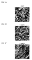
- FIG. 3A through FIG. 3C are AFM images of the surface of the substrate after the hydrogen heat treatment in the (111) substrate A.
- FIG. 3A is the AFM image of the germanium substrate 10 that underwent the hydrogen heat treatment in FIG. 1B at a temperature of 500°C for 1 minute
- FIG. 3B is the AFM image of the germanium substrate 10 that underwent the hydrogen heat treatment at a temperature of 500°C for 5 minutes
- FIG. 3C is the AFM image of the germanium substrate 10 that underwent the hydrogen heat treatment at a temperature of 500°C for 15 minutes.
- the AFM image corresponds to an area of 1 ⁇ m ⁇ 1 ⁇ m (a 1 ⁇ m square area).
- a step and terrace structure is not observed on the surface of the germanium substrate 10.
- FIG. 3B when the heat treatment time is 5 minutes, a small step and terrace structure is observed on the surface of the germanium substrate 10.
- FIG. 3C when the heat treatment time is 15 minutes, a step and terrace structure is observed on the surface of the germanium substrate 10.
- the surface on which a step and terrace structure is observed has a high flatness.
- FIG. 2 is compared with FIG. 3A through FIG. 3C .
- the mobility increases in the region where the surface electron density is high. This is considered to be because the flatness of the interface between the germanium substrate 10 and the germanium oxide film 12 improves as the heat treatment time increases.
- FIG. 4A through FIG. 4F are diagrams illustrating AFM observations of the surface of the substrate A after the hydrogen heat treatment in the (111) substrate A.
- FIG. 4A is the AFM observation image of the surface of the (111) substrate A that has undergone the hydrogen heat treatment at 500°C
- FIG. 4B is the AFM observation image of the surface of the (111) substrate A that has undergone the hydrogen heat treatment at 650°C
- FIG. 4C is the AFM observation image of the surface of the (111) substrate A that has undergone the hydrogen heat treatment at 850°C.
- the heat treatment time is 15 minutes.
- the area of the image is a 1 ⁇ m square area.
- FIG. 4D through FIG. 4F respectively illustrate the surface in the film thickness direction of the substrate to the surface direction of the substrate in a partial region of FIG. 4A through FIG. 4C , and correspond to cross-sections.
- the height of the step is approximately 0.3 nm or twice as high as approximately 0.3 nm.
- Germanium takes a diamond structure, and has a lattice constant of 0.567 nm.
- the thickness of a single layer of atoms based on a regular tetrahedral bonding structure making up the diamond structure is 0.567 ⁇ 3 -1/2 nm and is approximately 0.33 nm. The thickness corresponds to two bonds between Ge atoms. Accordingly, as illustrated in FIG. 4D through FIG.
- the height of the step corresponds to approximately one atomic layer.
- the temperature of the hydrogen heat treatment is between 500°C and 850°C, a step and terrace structure is formed on the surface of the germanium substrate 10.
- FIG. 5 is a graph of temperature of hydrogen heat treatment of the substrates A with different crystal orientations versus RMS (Root Mean Square) in a 1 ⁇ m square area.
- the heat treatment time is 15 minutes.
- the dots represent measurement points, and the lines represent approximate lines.
- the RMS of the substrate before the hydrogen heat treatment is approximately 0.3 nm.
- the (111) substrate A is indicated by (111).
- the substrate A having a (110) principal plane is indicated by (110), and the substrate A having a (100) principal plane is indicated by (100).
- the (111) and (110) substrates As illustrated in FIG. 5 , in the (111) and (110) substrates, a step and terrace structure was observed at all temperatures at intervals of 50°C between 500°C and 850°C.
- the black circles indicate that a step and terrace structure was observed, and the open circles indicate that a step and terrace structure was not observed.
- the heat treatment temperature is 700°C or greater
- a step and terrace structure is observed.
- the RMS of the substrate surface can be reduced to less than approximately 0.3 nm.
- the RMS is 0.2 nm or less within the temperature range between 500°C and 850°C.
- the RMS is 0.2 nm or less within the temperature range between 550°C and 750°C. In the (100) substrate, the RMS is 0.2 nm or less within the temperature range equal to or greater than 700°C.
- the hydrogen heat treatment planarizes the surface of the germanium substrate 10 almost regardless of the plane orientation of the germanium substrate 10.
- FIG. 6A through FIG. 6E are diagrams illustrating AFM observations of the surface of the substrate after the heat treatment in the (111) substrate A.
- FIG. 6A is the AFM observation image of the surface of the (111) substrate A that has undergone heat treatment in a hydrogen gas atmosphere
- FIG. 6B is the AFM observation image of the surface of the (111) substrate A that has undergone heat treatment in a nitrogen gas atmosphere (nitrogen heat treatment).
- the heat treatment temperature is 750°C
- the heat treatment time is 15 minutes.
- the area of the image is a 1 ⁇ m square area.
- FIG. 6C is a diagram illustrating the surface in the film thickness of the substrate with respect to the surface direction of the substrate in a partial region of FIG. 6B , and corresponds to the cross-section.
- FIG. 6D is the AFM observation image (perspective view) of the surface of the substrate A that has undergone heat treatment in a hydrogen gas atmosphere
- FIG. 6E is the AFM observation image (perspective view) of the surface of the substrate A that has undergone heat treatment in a nitrogen gas atmosphere.
- the area of the image is a 20 ⁇ m square area.
- the RMS in a 1 ⁇ m square area by the hydrogen heat treatment is approximately 0.2 nm, while the RMS in a 1 ⁇ m square area by the nitrogen heat treatment is approximately 0.2 to 0.5 nm.
- the surface of the germanium substrate is planarized even when the heat treatment is conducted not in a hydrogen gas atmosphere but in an inert gas atmosphere such as a nitrogen gas.
- an inert gas atmosphere such as a nitrogen gas.
- the surface of the germanium substrate 10 is planarized by heat treatment without oxidizing the surface of the germanium substrate 10. That is to say, the gas used in the heat treatment may be any of a reducing gas and an inert gas.
- the experimental results presented in FIG. 2 through FIG. 6E reveal that the surface of the germanium substrate 10 is planarized when the heat treatment is conducted in a reducing gas atmosphere or in an inert gas atmosphere at a temperature of approximately 500°C or greater.
- the surface of the germanium substrate 10 is planarized, the mobility in the region with a high surface electron concentration improves as illustrated in FIG. 2 .
- the flatness is almost the same when the heat treatment temperature is between 500°C and 850°C.
- the heat treatment temperature is around 500°C, the flatness depends on the heat treatment time.
- the mobility ⁇ eff of the substrate B having a (111) plane as a principal plane was measured by a split CV method.
- the germanium substrate 10 has an acceptor concentration N A of 2 ⁇ 10 15 cm -3 .
- the (111) substrate B has a maximum mobility of approximately 300 cm 2 /Vs.
- FIG. 7 is a graph of depth versus oxygen concentration in the (111) substrate B.
- the black circles represent the results of the SIMS analysis before the (111) substrate B underwent the hydrogen heat treatment
- the black triangles represent the results of the SIMS analysis after the (111) substrate B underwent the hydrogen heat treatment at 700°C
- the open circles represent the results of the SIMS analysis after the (111) substrate B underwent the hydrogen heat treatment at 850°C.
- the heat treatment temperature is 15 minutes.
- the oxygen concentration is 1 ⁇ 10 16 cm -3 or greater at a depth from the surface of less than at least 2 ⁇ m.
- the oxygen concentration is 1.5 ⁇ 10 16 cm -3 or greater at a depth from the surface of less than 1 ⁇ m.
- the oxygen concentration is below the detection limit.
- the substrate B has an oxygen concentration greater than the oxygen concentration of the substrate A.
- the low mobility in the substrate B has some kind of relationship with the oxygen concentration in the germanium substrate 10.
- the oxygen concentration in the substrate B decreases to 1 ⁇ 10 16 cm -3 or less.
- the oxygen concentration in the substrate B becomes 4 ⁇ 10 15 cm -3 , which is the detection limit, or less.
- the temperature of the hydrogen heat treatment is increased, the oxygen concentration in the germanium substrate 10 decreases.
- FIG. 8 is a graph of surface electron density N s versus mobility ⁇ eff in the (111) substrate B.
- the heat treatment temperature in FIG. 1B is 650°C, 750°C, and 850°C, and the heat treatment time is 15 minutes.
- the reference sample is a sample without undergoing the heat treatment in FIG. 1B , has a film thickness of a germanium oxide film of 15 nm, and the film formation temperature of the germanium oxide film is high.
- the reference sample has a maximum mobility of approximately 300 cm 2 /Vs.
- the maximum mobility improves to approximately 600 cm 2 /Vs.
- the maximum mobility further improves to approximately 800 cm 2 /Vs.
- the maximum mobility is approximately 1200 cm 2 /Vs, and almost the same as that of the substrate A.
- the heat treatment temperature is preferably 750°C or greater, more preferably 800°C or greater, further preferably 850°C or greater. Since the melting point of germanium is approximately 938°C, the heat treatment temperature is preferably 925°C or less, more preferably 900°C or less.
- oxygen ions were ion implanted into the germanium substrate 10 of the (111) substrate A, and the heat treatment was then conducted.
- a sample heat-treated in a nitrogen gas atmosphere and a sample heat-treated in a hydrogen gas atmosphere were fabricated.
- the fabrication process is the same as that of the (111) substrate A illustrated in FIG. 2 except the ion implantation and the heat treatment.
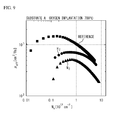
- FIG. 9 is a graph of surface electron density N s versus mobility ⁇ eff of the sample fabricated by ion implanting oxygen ions into the (111) substrate A.
- the heat treatment temperature in FIG. 1B is 700°C, and the heat treatment time is 15 minutes.
- the reference sample is the same as the reference sample of FIG. 2 without undergoing the ion implantation of oxygen and the hydrogen heat treatment. As illustrated in FIG. 9 , the reference sample has a maximum mobility of approximately 1200 cm 2 /Vs.
- the sample that underwent the nitrogen heat treatment after the oxygen ion implantation has a maximum mobility of approximately 500 cm 2 /Vs.
- the sample that underwent the hydrogen heat treatment after the oxygen ion implantation has a maximum mobility of approximately 800 cm 2 /Vs.
- the mobility decreases. The mobility is not much improved even when the nitrogen heat treatment is conducted after the oxygen ion implantation. In contrast, the mobility improves when the hydrogen heat treatment is conducted.
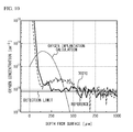
- FIG. 10 is a graph of depth from the surface versus oxygen concentration of a sample fabricated by ion implanting oxygen ions into the (111) substrate A.
- the solid line represents the results of the SIMS analysis of the reference sample before the hydrogen heat treatment
- the dashed line represents the results of the SIMS analysis of the sample after the hydrogen heat treatment at 700°C
- the dotted line represents the calculation result of oxygen ions that were ion implanted.
- the oxygen concentrations of the results of the SIMS analysis indicated by the solid line and the dashed line are very high in a region where the depth is less than 150 nm. This is because oxygen absorbed by the surface of the germanium substrate 10 is observed.
- the results in the region where the depth is less than 150 nm are not accurate.
- the detection limit and the behavior in the region where the depth is low differ from those of FIG. 7 .
- the substrate A before oxygen ions are implemented has an oxygen concentration of approximately 8 ⁇ 10 15 cm -3 , which is the detection limit.
- oxygen ions are ion implanted into the germanium substrate 10 so that the oxygen concentration takes a peak of 5 ⁇ 10 17 cm -3 at a depth of approximately 150 nm.
- the oxygen concentration is 3 ⁇ 10 16 cm -3 at a maximum when the depth is between 150 nm and 600 nm.
- the oxygen concentration is the detection limit.
- FIG. 10 reveals that the oxygen concentration in the germanium substrate 10 is reduced by hydrogen heat-treating the oxygen-implanted germanium substrate 10. As illustrated in FIG. 9 , the hydrogen heat treatment increases the mobility more than the nitrogen heat treatment. Thus, it is considered that the hydrogen heat treatment removes oxygen in the germanium substrate 10 and the mobility thus improves.
- the experimental results presented in FIG. 7 through FIG. 10 demonstrate that oxygen in the substrate B is removed and the oxygen concentration is reduced when the substrate B is heat-treated in a reducing gas atmosphere at approximately 700°C or greater.
- the oxygen concentration in the substrate B decreases, the mobility of the substrate B at room temperature becomes approximately the same as the mobility of the substrate A as illustrated in FIG. 9 . Accordingly, the defect affecting the mobility is considered to have a relation with oxygen in the substrate B.
- FIG. 11 is a schematic diagram illustrating surface electron density N s versus mobility ⁇ eff in the substrate.
- a region 50 where the surface electron density is high and a region 52 where the surface electron density is low will be considered.
- the mobility decreases.
- the region 52 as the surface electron density decreases, the mobility decreases.
- the region 50 is considered to be a region where the mobility is limited by mainly the flatness of the surface of the germanium substrate 10.
- the flatness of the surface of the germanium substrate 10 improves. As illustrated in FIG. 5 , the flatness of the surface of the germanium substrate 10 remains approximately the same even when the heat treatment temperature is increased to greater than 500°C.
- the region 52 is considered to be a region where the mobility is limited by mainly the scattering due to the defect relating to oxygen in the germanium substrate 10.
- the oxygen concentration in the germanium substrate 10 is low.
- the oxygen concentration in the germanium substrate 10 before the heat treatment in a reducing gas atmosphere is high, and the defect relating to oxygen is formed.
- the oxygen concentration in the germanium substrate 10 decreases. The oxygen concentration decreases as the heat treatment temperature increases.
- the substrate A has less defects in the germanium substrate 10.
- the mobility in the region 52 is high even before the hydrogen heat treatment in a reducing gas atmosphere.
- the flatness of the surface of the germanium substrate 10 is bad before the heat treatment.
- the mobility is low.
- the flatness of the surface of the germanium substrate 10 improves, the mobility in the region 50 improves.
- the substrate B has many defects in the germanium substrate 10.
- the mobility in the region 52 before the heat treatment in a reducing gas atmosphere is low.
- the defects in the germanium substrate 10 decrease, and the mobility in the region 52 improves.
- the flatness of the surface of the germanium substrate 10 improves.
- the heat treatment temperature is less than 700°C
- the mobility in the region 50 does not improve as much as that of the substrate A because of the effect of the defect in the germanium substrate 10.
- the temperature of the heat treatment in a reducing gas atmosphere is 700°C or greater, the defects relating to oxygen in the germanium substrate 10 decrease, and the mobility in the regions 50 and 52 improves.
- the flatness of the surface of the germanium substrate 10 and defects relating to oxygen in the germanium substrate 10 affect the mobility.
- the flatness is considered to equally affect the substrate A and the substrate B.
- the substrate B has more defects relating to oxygen.
- the defects are considered the cause of the low mobility in the substrate B. Therefore, the heat treatment is conducted in a reducing gas atmosphere at 700°C or greater. This reduces the oxygen concentration in the germanium substrate 10, and improves the mobility.
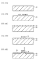
- FIG. 12A through FIG. 12E are cross-sectional views illustrating a method of manufacturing a semiconductor device of a first embodiment.
- a germanium layer 30 having an oxygen concentration of 1 ⁇ 10 16 cm -3 or greater.
- the germanium layer 30 may be a single crystal germanium substrate, or may be a germanium film formed on a substrate (for example, a silicon substrate).
- the germanium layer 30 may be high-purity germanium, or may contain impurities.
- the germanium layer 30 may be n-type or p-type germanium.
- the germanium layer 30 may contain silicon as long as the effect of the above experiments is obtained.
- the composition ratio of silicon is required to be approximately 10% or less of the total.
- the principal plane of the germanium layer 30 may be any plane, and may be, for example, a (100) plane, a (111) plane, or a (110) plane.
- the (100) plane, the (111) plane, and the (110) plane respectively include crystal planes equivalent to the (100) plane, the (111) plane, and the (110) plane.
- the principal plane may be a few degrees off from these planes. That is to say, the normal direction of the principal plane may be inclined at a few degrees or less, preferably one degree or less, from the ⁇ 111> orientation or the ⁇ 110> orientation.
- the surface of the germanium layer 30 is heat-treated in a reducing gas atmosphere at 700°C or greater.
- the reducing gas is a gas that hardly reacts with the germanium layer 30 by the heat treatment and reduces (or removes) oxygen in the germanium layer 30.
- a hydrogen gas may be used as the reducing gas, for example.
- mixed gas of a hydrogen gas and an inert gas may be used.
- the inert gas include, for example, nitrogen gas, and a gas of the XVIII-family element such as helium (He), neon (Ne), argon (Ar), krypton (Kr), xenon (Xe) or radon (Rn).
- the reducing gas may not contain a hydrogen gas.
- a gas containing little oxygen and hardly reacting with the germanium layer 30 by the heat treatment may be used as long as the gas removes oxygen in the germanium layer 30 by the heat treatment.
- a nitrogen gas containing little oxygen may be used.
- the gas used for the heat treatment preferably contains little oxygen.
- the gas pressure of the heat treatment may be 1 atm, less than 1 atm, or greater than 1 atm.
- a gate insulating film 32 is formed on the surface of the germanium substrate 10.
- a germanium oxide film, a high permittivity insulating film, or a multilayered film of a germanium oxide film and a high permittivity insulating film may be used.
- a rare-earth metal oxide film such as hafnium oxide, zirconium oxide, or yttrium oxide may be used.
- the film thickness of the gate insulating film 32 is preferably 2 nm or less, more preferably 1.5 nm or less, further preferably 1.0 nm or less.
- a gate electrode 34 is formed on the gate insulating film 32.
- a conductive layer such as a metal or a semiconductor may be used.
- a source or drain region 38 is formed on the germanium layer 30 at both sides of the electrode 34.
- the germanium layer 30 is p-type, and the source or drain region 38 is n-type.
- the germanium layer 30 may be n-type, and the source or drain region 38 may be p-type.
- the use of the germanium layer 30 having a (111) plane as a principal plane improves the performance.
- the use of the germanium layer 30 having a (100) plane or a (110) plane as a principal plane improves the performance.
- the surface of the germanium layer 30 having an oxygen concentration of 1 ⁇ 10 16 cm -3 or greater is heat-treated in a reducing gas atmosphere at 700°C or greater. This improves the mobility of the germanium layer 30, and improves the performance of the semiconductor device.
- the heat treatment is conducted preferably in a reducing gas atmosphere.
- the heat treatment in a reducing gas atmosphere reduces the oxygen concentration of the germanium layer 30 to less than 1 ⁇ 10 16 cm -3 . Accordingly, the mobility of the germanium layer 30 is improved.
- the oxygen concentration is preferably 8 ⁇ 10 15 cm -3 or less, more preferably 5 ⁇ 10 15 cm -3 or less.
- the heat treatment temperature is preferably 750°C or greater, more preferably a temperature greater than 800°C, more preferably 800°C or greater, further preferably 850°C or greater.
- the heat treatment time is preferably 1 minute or greater, more preferably 5 minutes or greater, further preferably 15 minutes or greater.
- the heat treatment temperature When the heat treatment time is long, the heat treatment temperature may be low. When the heat treatment temperature is high, the heat treatment time may be short. The heat treatment is required to be conducted so that the oxygen concentration of the germanium layer 30 is reduced.
- the first embodiment describes a MOSFET as an example. However, the first embodiment can be applied to semiconductor devices other than the MOSFET.
- the first embodiment mainly describes a semiconductor device.
- the execution of the process to FIG. 12B enables to manufacture a semiconductor substrate.
- the semiconductor substrate may be a single crystal germanium substrate, or a substrate formed by forming a germanium layer on a support substrate such as a silicon substrate or a glass substrate.
- the germanium layer may be any of single crystal, multicrystal, and amorphous.
- FIG. 13 is a graph of depth versus oxygen concentration in the (111) substrate B.
- the black squares represent the results of the SIMS analysis before the (111) substrate B underwent the hydrogen heat treatment
- the black triangles represent the results of the SIMS analysis after the (111) substrate B underwent the hydrogen heat treatment at 700°C
- the black circles represent the results of the SIMS analysis after the (111) substrate B underwent the hydrogen heat treatment at 850°C.
- the detection limit of oxygen is approximately 1 ⁇ 10 15 cm -3 .
- the oxygen concentration is 1 ⁇ 10 16 cm -3 or greater at a depth of less than at least 5 ⁇ m.
- the oxygen concentration in the substrate B decreases to 1 ⁇ 10 16 cm -3 or less.
- the oxygen concentration decreases.
- the oxygen concentration is approximately 5x10 15 cm -3 or less.
- the oxygen concentration is approximately 4 ⁇ 10 15 cm -3 or less.
- the oxygen concentration is approximately 5x10 15 cm -3 or less. At a depth of 1.5 ⁇ m or less, the oxygen concentration is approximately 2x10 15 cm -3 .
- the oxygen concentration in the germanium substrate 10 decreases. The oxygen concentration in the channel region near the surface of the germanium substrate cannot be detected, but is considered to be almost the same as the oxygen concentration at a depth of approximately 1 ⁇ m.
- FIG. 13 When FIG. 13 is compared with FIG. 8 , as the temperature of the hydrogen heat treatment increases, the oxygen concentration in the substrate B decreases, and the electron mobility improves.
- the temperature of the hydrogen heat treatment is 700°C
- the oxygen concentration in the channel region is considered to be approximately 4 ⁇ 10 15 cm -3 .
- the peak electron mobility is 500 to 700 cm 2 /Vs.
- the heat treatment temperature is 850°C
- the oxygen concentration in the channel region is considered to be approximately 2 ⁇ 10 15 cm -3
- the electron mobility is approximately the same as that of the substrate A illustrated in FIG. 2 .
- the heat treatment temperature is configured to be 850°C or greater, the oxygen concentration in the channel region becomes approximately 2 ⁇ 10 16 cm -3 or less. This configuration enables to achieve the electron mobility approximately same as the electron mobility of the substrate A.
Landscapes
- Thin Film Transistor (AREA)
- Recrystallisation Techniques (AREA)
- Insulated Gate Type Field-Effect Transistor (AREA)
- Crystals, And After-Treatments Of Crystals (AREA)
- Semiconductor Memories (AREA)
- Physical Vapour Deposition (AREA)
Abstract
Description
- The present invention relates to a method of manufacturing a semiconductor substrate and a method of manufacturing a semiconductor device, and more particularly to a method of manufacturing a semiconductor substrate in which a germanium layer is heat-treated and a method of manufacturing a semiconductor device in which a germanium layer is heat-treated.
- Germanium (Ge) is a semiconductor having electronic properties better than those of silicon (Si). For example, a MOSFET (Metal Oxide Semiconductor Field Effect Transistor) using germanium has been developed. For example, in the MOSFET, it is important to improve the mobility of a carrier in a germanium layer.
- Non-Patent Document 1: Extended Abstract of the 2011 International Conference on Solid State Devices and Materials, Nagoya, 2011, pp 925-926
- In a single crystal germanium substrate, the mobility greatly differs depending on the type of the substrate. When the mobility of the germanium substrate is low, high performance is not obtained in a semiconductor device such as a MOSFET. It is required to improve the mobility of the germanium layer and enhance the performance of the semiconductor device.
- The present invention has been made in the view of the above problems, and aims to provide a high-performance semiconductor device.
- The present invention is a method of manufacturing a semiconductor substrate characterized by including: heat-treating a germanium layer having an oxygen concentration of 1×1016 cm-3 or greater in a reducing gas atmosphere at 700°C or greater.
- The present invention is a method of manufacturing a semiconductor substrate characterized by including: heat-treating a germanium layer having an oxygen concentration of 1×1016 cm-3 or greater in a reducing gas atmosphere so that the oxygen concentration decreases.
- In the above configuration, the heat-treating may be configured to include heat-treating the germanium layer at 800°C or greater.
- In the above configuration, the oxygen concentration of the germanium layer may be configured to become less than 1×1016 cm-3 by the heat-treating.
- In the above configuration, the germanium layer may be configured to have a (111) plane as a principal plane.
- In the above configuration, the reducing gas atmosphere may be configured to be a hydrogen gas atmosphere.
- In the above configuration, the germanium layer may be configured to be a single crystal germanium substrate.
- The present invention is a method of manufacturing a semiconductor device characterized by including: forming a semiconductor device on a semiconductor substrate manufactured by the above method of manufacturing a semiconductor substrate.
- In the above configuration, the forming of the semiconductor device may be configured to include: forming a gate insulating film on a surface of the germanium layer that has undergone the heat-treating; and forming a gate electrode on the gate insulating film.
- The present invention provides a high-performance semiconductor device.
-
-
FIG. 1A through FIG. 1D are cross-sectional views illustrating a method of fabricating a MOS structure that was used for an experiment; -
FIG. 2 is a graph of surface electron density Ns versus mobility µeff in a (111) substrate A; -
FIG. 3A through FIG. 3C are AFM images of the surface of a substrate after hydrogen heat treatment in the (111) substrate A; -
FIG. 4A through FIG. 4F are diagrams illustrating AFM observations after hydrogen heat treatment in the (111) substrate A; -
FIG. 5 is a graph of heat treatment temperature in hydrogen heat treatment of substrates A with different crystal orientations versus RMS within a 1 µm square area; -
FIG. 6A through FIG. 6E are diagrams illustrating AFM observations of the surface of the substrate A after heat treatment in the (111) substrate A; -
FIG. 7 is a graph of depth versus oxygen concentration in a (111) substrate B; -
FIG. 8 is a graph of surface electron density Ns versus mobility µeff in the (111) substrate B; -
FIG. 9 is a graph of surface electron density Ns versus mobility µeff of a sample fabricated by ion implanting oxygen ions into the (111) substrate A; -
FIG. 10 is a graph of depth from the surface versus oxygen concentration of a sample fabricated by ion implanting oxygen ions into the (111) substrate A; -
FIG. 11 is a schematic diagram illustrating surface electron density Ns versus mobility µeff in the substrate B; -
FIG. 12A through FIG. 12E are cross-sectional views illustrating a method of manufacturing a semiconductor device in accordance with a first embodiment; and -
FIG. 13 is a graph of depth versus oxygen concentration in the (111) substrate B. - When a MOS structure is fabricated with a single crystal germanium substrate and the mobility thereof is measured, the mobility differs depending on the type of the substrate. As an example, the mobility differs depending on a growth system that grows a substrate, growth conditions, and materials. However, it is not clear yet whether the difference in mobility depends on the growth procedure itself, or any other factor. Moreover, the mobility differs also in a germanium layer formed on the substrate. The reason why the mobility differs depending on the type of the substrate or the type of the layer is not clear yet. Therefore, the mobility is difficult to improve.
- To investigate the reason why the mobility differs depending on the type of the substrate or the type of the layer, a substrate A and a substrate B of which the growth procedures differ from each other were prepared as single crystal germanium substrates having different mobilities. The substrate B has a mobility lower than the mobility of the substrate A. MOS structures were fabricated with the substrate A and the substrate B, and the following experiment was conducted.
- FIG. lea through
FIG. 1D are cross-sectional views illustrating a method of fabricating a MOS structure that was used for the experiment. As illustrated inFIG. 1A , a P-type singlecrystal germanium substrate 10 is prepared. As the single crystal germanium substrate, the substrate A or the substrate B is used. In the following description, the substrate A having a (111) plane as a principal plane is referred to as a (111) substrate A, and the substrate B having a (111) plane as a principal plane is referred to as a (111) substrate B. Thegermanium substrate 10 has an acceptor concentration NA of 2×1015 cm-3. - As illustrated in
FIG. 1B , heat treatment is conducted in a hydrogen (H2) gas atmosphere (100% hydrogen gas atmosphere) at a pressure of 1 atm. Hereinafter, the heat treatment in a hydrogen gas atmosphere is also referred to as hydrogen heat treatment. As illustrated inFIG. 1C , agermanium oxide film 12 is formed on thegermanium substrate 10. Thegermanium oxide film 12 is formed by heat-treating thegermanium substrate 10 in an oxygen gas atmosphere. Thegermanium oxide film 12 is formed at an oxygen pressure of 70 atm at a substrate temperature of 500°C. Thegermanium oxide film 12 has a film thickness of approximately 5 to 6 nm. As illustrated inFIG. 1D , a gold (Au) film as ametal film 14 is formed on the surface of thegermanium oxide film 12. Themetal film 14 is used as a gate electrode. - With use of the (111) substrate A, fabricated was a MOS structure having a gate length of 100 µm and a gate width of 25 µm. The carrier number and the mobility µeff at room temperature are obtained by a split CV method. The split CV method derives the carrier number from the integral of the CV measurement, and calculates the mobility from the carrier number and the I-V measurement. The surface electron density Ns was calculated from the carrier number.
-
FIG. 2 is a graph of surface electron density Ns versus mobility µeff in the (111) substrate A. Gate voltage was applied to the gate electrode to change the surface electron density Ns, and the mobility µeff was measured. The hydrogen heat treatment inFIG. 1B was conducted at a temperature of 500°C for 1 minute, 5 minutes, and 15 minutes. The reference sample is a sample without undergoing the hydrogen heat treatment ofFIG. 1B , has a film thickness of a germanium oxide film of 15 nm, and the film formation temperature of the germanium oxide film is high. The reference sample has a maximum mobility of approximately 1200 cm2/Vs when the surface electron density is 4×1011 cm-2. In the region where the surface electron density is lower than the peak of the mobility, the mobility hardly changes with respect to the heat treatment time. In the region where the surface electron density is higher than the peak of the mobility, the mobility increases as the heat treatment time increases. As the surface electron density increases, the difference in mobility due to the heat treatment time increases. - After
FIG. 1B , the surface of thegermanium substrate 10 of the substrate A was observed by AFM (Atomic Force Microcopy).FIG. 3A through FIG. 3C are AFM images of the surface of the substrate after the hydrogen heat treatment in the (111) substrate A.FIG. 3A is the AFM image of thegermanium substrate 10 that underwent the hydrogen heat treatment inFIG. 1B at a temperature of 500°C for 1 minute,FIG. 3B is the AFM image of thegermanium substrate 10 that underwent the hydrogen heat treatment at a temperature of 500°C for 5 minutes, andFIG. 3C is the AFM image of thegermanium substrate 10 that underwent the hydrogen heat treatment at a temperature of 500°C for 15 minutes. The AFM image corresponds to an area of 1 µm×1µm (a 1 µm square area). As illustrated inFIG. 3A , when the heat treatment time is 1 minute, a step and terrace structure is not observed on the surface of thegermanium substrate 10. As illustrated inFIG. 3B , when the heat treatment time is 5 minutes, a small step and terrace structure is observed on the surface of thegermanium substrate 10. As illustrated inFIG. 3C , when the heat treatment time is 15 minutes, a step and terrace structure is observed on the surface of thegermanium substrate 10. As described above, when the heat treatment time is long, a step and terrace structure is observed. The surface on which a step and terrace structure is observed has a high flatness. -
FIG. 2 is compared withFIG. 3A through FIG. 3C . At a heat treatment time of 500°C, as the heat treatment time increases, the mobility increases in the region where the surface electron density is high. This is considered to be because the flatness of the interface between thegermanium substrate 10 and thegermanium oxide film 12 improves as the heat treatment time increases. - Thus, for the (111) substrate A, conducted was an experiment in the planarization of the surface of the
germanium substrate 10 by heat treatment. -
FIG. 4A through FIG. 4F are diagrams illustrating AFM observations of the surface of the substrate A after the hydrogen heat treatment in the (111) substrate A.FIG. 4A is the AFM observation image of the surface of the (111) substrate A that has undergone the hydrogen heat treatment at 500°C,FIG. 4B is the AFM observation image of the surface of the (111) substrate A that has undergone the hydrogen heat treatment at 650°C, andFIG. 4C is the AFM observation image of the surface of the (111) substrate A that has undergone the hydrogen heat treatment at 850°C. The heat treatment time is 15 minutes. The area of the image is a 1 µm square area.FIG. 4D through FIG. 4F respectively illustrate the surface in the film thickness direction of the substrate to the surface direction of the substrate in a partial region ofFIG. 4A through FIG. 4C , and correspond to cross-sections. - As illustrated in
FIG. 4A through FIG. 4C , when the heat treatment temperature was between 500°C and 850°C, a step and terrace structure is observed. As illustrated inFIG. 4D through FIG. 4F , the height of the step is approximately 0.3 nm or twice as high as approximately 0.3 nm. Germanium takes a diamond structure, and has a lattice constant of 0.567 nm. In the (111) plane, the thickness of a single layer of atoms based on a regular tetrahedral bonding structure making up the diamond structure is 0.567×3-1/2 nm and is approximately 0.33 nm. The thickness corresponds to two bonds between Ge atoms. Accordingly, as illustrated inFIG. 4D through FIG. 4F , the height of the step corresponds to approximately one atomic layer. As described above, in the (111) substrate A, when the temperature of the hydrogen heat treatment is between 500°C and 850°C, a step and terrace structure is formed on the surface of thegermanium substrate 10. -
FIG. 5 is a graph of temperature of hydrogen heat treatment of the substrates A with different crystal orientations versus RMS (Root Mean Square) in a 1 µm square area. The heat treatment time is 15 minutes. The dots represent measurement points, and the lines represent approximate lines. The RMS of the substrate before the hydrogen heat treatment is approximately 0.3 nm. The (111) substrate A is indicated by (111). The substrate A having a (110) principal plane is indicated by (110), and the substrate A having a (100) principal plane is indicated by (100). - As illustrated in
FIG. 5 , in the (111) and (110) substrates, a step and terrace structure was observed at all temperatures at intervals of 50°C between 500°C and 850°C. In the (100) substrate, the black circles indicate that a step and terrace structure was observed, and the open circles indicate that a step and terrace structure was not observed. In the (100) substrate, when the heat treatment temperature is 700°C or greater, a step and terrace structure is observed. In the (111), (110), and (100) substrates, within the temperature range between 500°C and 850°C, the RMS of the substrate surface can be reduced to less than approximately 0.3 nm. In the (110) substrate, the RMS is 0.2 nm or less within the temperature range between 500°C and 850°C. In the (111) substrate, the RMS is 0.2 nm or less within the temperature range between 550°C and 750°C. In the (100) substrate, the RMS is 0.2 nm or less within the temperature range equal to or greater than 700°C. - As described above, the hydrogen heat treatment planarizes the surface of the
germanium substrate 10 almost regardless of the plane orientation of thegermanium substrate 10. - The atmosphere of the heat treatment was changed, and an experiment in the planarization of the surface of the
germanium substrate 10 was conducted.FIG. 6A through FIG. 6E are diagrams illustrating AFM observations of the surface of the substrate after the heat treatment in the (111) substrate A.FIG. 6A is the AFM observation image of the surface of the (111) substrate A that has undergone heat treatment in a hydrogen gas atmosphere, andFIG. 6B is the AFM observation image of the surface of the (111) substrate A that has undergone heat treatment in a nitrogen gas atmosphere (nitrogen heat treatment). The heat treatment temperature is 750°C, and the heat treatment time is 15 minutes. The area of the image is a 1 µm square area.FIG. 6C is a diagram illustrating the surface in the film thickness of the substrate with respect to the surface direction of the substrate in a partial region ofFIG. 6B , and corresponds to the cross-section.FIG. 6D is the AFM observation image (perspective view) of the surface of the substrate A that has undergone heat treatment in a hydrogen gas atmosphere, andFIG. 6E is the AFM observation image (perspective view) of the surface of the substrate A that has undergone heat treatment in a nitrogen gas atmosphere. The area of the image is a 20 µm square area. - As demonstrated in
FIG. 6B and FIG. 6C , when the nitrogen heat treatment was conducted, a step and terrace structure is observed. The RMS in a 1 µm square area by the hydrogen heat treatment is approximately 0.2 nm, while the RMS in a 1 µm square area by the nitrogen heat treatment is approximately 0.2 to 0.5 nm. - As described above, the surface of the germanium substrate is planarized even when the heat treatment is conducted not in a hydrogen gas atmosphere but in an inert gas atmosphere such as a nitrogen gas. This demonstrates that the surface of the
germanium substrate 10 is planarized by heat treatment without oxidizing the surface of thegermanium substrate 10. That is to say, the gas used in the heat treatment may be any of a reducing gas and an inert gas. - The experimental results presented in
FIG. 2 through FIG. 6E reveal that the surface of thegermanium substrate 10 is planarized when the heat treatment is conducted in a reducing gas atmosphere or in an inert gas atmosphere at a temperature of approximately 500°C or greater. When the surface of thegermanium substrate 10 is planarized, the mobility in the region with a high surface electron concentration improves as illustrated inFIG. 2 . As illustrated inFIG. 5 , the flatness is almost the same when the heat treatment temperature is between 500°C and 850°C. As illustrated inFIG. 3A through FIG. 3C , when the heat treatment temperature is around 500°C, the flatness depends on the heat treatment time. Although the experimental results of the substrate A have been described, the surface of the substrate is also planarized in the substrate B as with the substrate A. As described above, the heat treatment planarizes the surface of the substrate regardless of the type of the substrate. - The mobility µeff of the substrate B having a (111) plane as a principal plane (referred to as a (111) substrate B) was measured by a split CV method. The
germanium substrate 10 has an acceptor concentration NA of 2×1015 cm-3. The (111) substrate B has a maximum mobility of approximately 300 cm2/Vs. - The substrate A and the substrate B were analyzed by SIMS (Secondary Ion Mass Spectroscopy).
FIG. 7 is a graph of depth versus oxygen concentration in the (111) substrate B. The black circles represent the results of the SIMS analysis before the (111) substrate B underwent the hydrogen heat treatment, the black triangles represent the results of the SIMS analysis after the (111) substrate B underwent the hydrogen heat treatment at 700°C, and the open circles represent the results of the SIMS analysis after the (111) substrate B underwent the hydrogen heat treatment at 850°C. The heat treatment temperature is 15 minutes. In the substrate B before the hydrogen heat treatment, the oxygen concentration is 1×1016 cm-3 or greater at a depth from the surface of less than at least 2 µm. The oxygen concentration is 1.5×1016 cm-3 or greater at a depth from the surface of less than 1 µm. On the other hand, in the (111) substrate A, the oxygen concentration is below the detection limit. As described above, the substrate B has an oxygen concentration greater than the oxygen concentration of the substrate A. Thus, it is estimated that the low mobility in the substrate B has some kind of relationship with the oxygen concentration in thegermanium substrate 10. - Furthermore, when the hydrogen heat treatment is conducted at 700°C, the oxygen concentration in the substrate B decreases to 1×1016 cm-3 or less. When the hydrogen heat treatment is conducted at 850°C, the oxygen concentration in the substrate B becomes 4×1015 cm-3, which is the detection limit, or less. As described above, as the temperature of the hydrogen heat treatment is increased, the oxygen concentration in the
germanium substrate 10 decreases. - For the (111) substrate B, samples that underwent hydrogen heat treatment at different heat treatment temperatures were fabricated to measure the mobility. The fabrication process is the same as the fabrication process of the (111) substrate A illustrated in
FIG. 2 except the substrate and the heat treatment.FIG. 8 is a graph of surface electron density Ns versus mobility µeff in the (111) substrate B. The heat treatment temperature inFIG. 1B is 650°C, 750°C, and 850°C, and the heat treatment time is 15 minutes. The reference sample is a sample without undergoing the heat treatment inFIG. 1B , has a film thickness of a germanium oxide film of 15 nm, and the film formation temperature of the germanium oxide film is high. The reference sample has a maximum mobility of approximately 300 cm2/Vs. When the heat treatment temperature is 650°C, the maximum mobility improves to approximately 600 cm2/Vs. When the heat treatment temperature is 750°C, the maximum mobility further improves to approximately 800 cm2/Vs. When the heat treatment temperature is 850°C, the maximum mobility is approximately 1200 cm2/Vs, and almost the same as that of the substrate A. - When
FIG. 7 is compared withFIG. 8 , as the temperature of the hydrogen heat treatment increases, the oxygen concentration in the substrate B decreases, and the mobility improves. When the temperature of the hydrogen heat treatment is 850°C, the oxygen concentration in the substrate B is approximately the detection limit, and the mobility is approximately the same as that of the substrate A. As described above, the oxygen concentration in thegermanium substrate 10 correlates with the mobility. To improve the mobility, the heat treatment temperature is preferably 750°C or greater, more preferably 800°C or greater, further preferably 850°C or greater. Since the melting point of germanium is approximately 938°C, the heat treatment temperature is preferably 925°C or less, more preferably 900°C or less. - It is not clear why the oxygen concentration decreases as the heat treatment temperature of the hydrogen heat treatment increases in the substrate B. It may be because oxygen in the
germanium substrate 10 is removed by a reducing gas, for example. - To confirm that the oxygen concentration in the germanium substrate is reduced by the hydrogen heat treatment, oxygen ions were ion implanted into the
germanium substrate 10 of the (111) substrate A, and the heat treatment was then conducted. A sample heat-treated in a nitrogen gas atmosphere and a sample heat-treated in a hydrogen gas atmosphere were fabricated. The fabrication process is the same as that of the (111) substrate A illustrated inFIG. 2 except the ion implantation and the heat treatment. -
FIG. 9 is a graph of surface electron density Ns versus mobility µeff of the sample fabricated by ion implanting oxygen ions into the (111) substrate A. The heat treatment temperature inFIG. 1B is 700°C, and the heat treatment time is 15 minutes. The reference sample is the same as the reference sample ofFIG. 2 without undergoing the ion implantation of oxygen and the hydrogen heat treatment. As illustrated inFIG. 9 , the reference sample has a maximum mobility of approximately 1200 cm2/Vs. The sample that underwent the nitrogen heat treatment after the oxygen ion implantation has a maximum mobility of approximately 500 cm2/Vs. Whereas the sample that underwent the hydrogen heat treatment after the oxygen ion implantation has a maximum mobility of approximately 800 cm2/Vs. As described above, when oxygen ions are implanted, the mobility decreases. The mobility is not much improved even when the nitrogen heat treatment is conducted after the oxygen ion implantation. In contrast, the mobility improves when the hydrogen heat treatment is conducted. - The sample that had undergone the hydrogen heat treatment at 700°C was analyzed by SIMS.
FIG. 10 is a graph of depth from the surface versus oxygen concentration of a sample fabricated by ion implanting oxygen ions into the (111) substrate A. The solid line represents the results of the SIMS analysis of the reference sample before the hydrogen heat treatment, the dashed line represents the results of the SIMS analysis of the sample after the hydrogen heat treatment at 700°C, and the dotted line represents the calculation result of oxygen ions that were ion implanted. The oxygen concentrations of the results of the SIMS analysis indicated by the solid line and the dashed line are very high in a region where the depth is less than 150 nm. This is because oxygen absorbed by the surface of thegermanium substrate 10 is observed. The results in the region where the depth is less than 150 nm are not accurate. In addition, as the measuring speed differs, the detection limit and the behavior in the region where the depth is low differ from those ofFIG. 7 . - As illustrated in
FIG. 10 , in the reference sample, the substrate A before oxygen ions are implemented has an oxygen concentration of approximately 8×1015 cm-3, which is the detection limit. As indicated by the calculation result represented by the dotted line, oxygen ions are ion implanted into thegermanium substrate 10 so that the oxygen concentration takes a peak of 5×1017 cm-3 at a depth of approximately 150 nm. - When the hydrogen heat treatment is conducted at 700°C, the oxygen concentration is 3×1016 cm-3 at a maximum when the depth is between 150 nm and 600 nm. When the depth is 600 nm or greater, the oxygen concentration is the detection limit.
FIG. 10 reveals that the oxygen concentration in thegermanium substrate 10 is reduced by hydrogen heat-treating the oxygen-implantedgermanium substrate 10. As illustrated inFIG. 9 , the hydrogen heat treatment increases the mobility more than the nitrogen heat treatment. Thus, it is considered that the hydrogen heat treatment removes oxygen in thegermanium substrate 10 and the mobility thus improves. - The experimental results presented in
FIG. 7 through FIG. 10 demonstrate that oxygen in the substrate B is removed and the oxygen concentration is reduced when the substrate B is heat-treated in a reducing gas atmosphere at approximately 700°C or greater. When the oxygen concentration in the substrate B decreases, the mobility of the substrate B at room temperature becomes approximately the same as the mobility of the substrate A as illustrated inFIG. 9 . Accordingly, the defect affecting the mobility is considered to have a relation with oxygen in the substrate B. - In light of the experimental results presented in
FIG. 2 through FIG. 10 , the behavior of the mobility with respect to the surface electron density will be described.FIG. 11 is a schematic diagram illustrating surface electron density Ns versus mobility µeff in the substrate. Aregion 50 where the surface electron density is high and aregion 52 where the surface electron density is low will be considered. In theregion 50, as the surface electron density increases, the mobility decreases. In theregion 52, as the surface electron density decreases, the mobility decreases. - The
region 50 is considered to be a region where the mobility is limited by mainly the flatness of the surface of thegermanium substrate 10. In theregion 50, when the heat treatment is conducted in a reducing gas atmosphere or an inert gas atmosphere at a temperature of 500°C or greater, the flatness of the surface of thegermanium substrate 10 improves. As illustrated inFIG. 5 , the flatness of the surface of thegermanium substrate 10 remains approximately the same even when the heat treatment temperature is increased to greater than 500°C. - The
region 52 is considered to be a region where the mobility is limited by mainly the scattering due to the defect relating to oxygen in thegermanium substrate 10. In the substrate A, even when the heat treatment is not conducted in a reducing gas atmosphere, the oxygen concentration in thegermanium substrate 10 is low. In contrast, in the substrate B, the oxygen concentration in thegermanium substrate 10 before the heat treatment in a reducing gas atmosphere is high, and the defect relating to oxygen is formed. When the substrate B is heat-treated in a reducing gas atmosphere, the oxygen concentration in thegermanium substrate 10 decreases. The oxygen concentration decreases as the heat treatment temperature increases. - The substrate A has less defects in the
germanium substrate 10. Thus, the mobility in theregion 52 is high even before the hydrogen heat treatment in a reducing gas atmosphere. In theregion 50, the flatness of the surface of thegermanium substrate 10 is bad before the heat treatment. Thus, the mobility is low. As illustrated inFIG. 2 , as the flatness of the surface of thegermanium substrate 10 improves, the mobility in theregion 50 improves. - The substrate B has many defects in the
germanium substrate 10. Thus, the mobility in theregion 52 before the heat treatment in a reducing gas atmosphere is low. When the heat treatment is conducted in a reducing gas atmosphere, the defects in thegermanium substrate 10 decrease, and the mobility in theregion 52 improves. In theregion 50, when the heat treatment is conducted at 500°C or greater, the flatness of the surface of thegermanium substrate 10 improves. However, when the heat treatment temperature is less than 700°C, the mobility in theregion 50 does not improve as much as that of the substrate A because of the effect of the defect in thegermanium substrate 10. As illustrated inFIG. 8 , when the temperature of the heat treatment in a reducing gas atmosphere is 700°C or greater, the defects relating to oxygen in thegermanium substrate 10 decrease, and the mobility in theregions - As described above, the flatness of the surface of the
germanium substrate 10 and defects relating to oxygen in thegermanium substrate 10 affect the mobility. The flatness is considered to equally affect the substrate A and the substrate B. The substrate B has more defects relating to oxygen. The defects are considered the cause of the low mobility in the substrate B. Therefore, the heat treatment is conducted in a reducing gas atmosphere at 700°C or greater. This reduces the oxygen concentration in thegermanium substrate 10, and improves the mobility. - In the MOS structure with use of a silicon substrate, it has been known that the oxygen concentration in the silicon substrate has little effect on the mobility, and the phenomenon that the mobility relates to oxygen is a unique phenomenon of a germanium substrate.
- An embodiment of the present invention based on the above experimental results will be described hereinafter.
-
FIG. 12A through FIG. 12E are cross-sectional views illustrating a method of manufacturing a semiconductor device of a first embodiment. As illustrated inFIG. 12A , prepared is agermanium layer 30 having an oxygen concentration of 1×1016 cm-3 or greater. When the scattering due to the defect is supposed to be the cause of the decrease in the mobility, thegermanium layer 30 may be a single crystal germanium substrate, or may be a germanium film formed on a substrate (for example, a silicon substrate). Alternatively, thegermanium layer 30 may be high-purity germanium, or may contain impurities. For example, thegermanium layer 30 may be n-type or p-type germanium. Furthermore, thegermanium layer 30 may contain silicon as long as the effect of the above experiments is obtained. The composition ratio of silicon is required to be approximately 10% or less of the total. The principal plane of thegermanium layer 30 may be any plane, and may be, for example, a (100) plane, a (111) plane, or a (110) plane. The (100) plane, the (111) plane, and the (110) plane respectively include crystal planes equivalent to the (100) plane, the (111) plane, and the (110) plane. The principal plane may be a few degrees off from these planes. That is to say, the normal direction of the principal plane may be inclined at a few degrees or less, preferably one degree or less, from the <111> orientation or the <110> orientation. - As illustrated in
FIG. 12B , the surface of thegermanium layer 30 is heat-treated in a reducing gas atmosphere at 700°C or greater. The reducing gas is a gas that hardly reacts with thegermanium layer 30 by the heat treatment and reduces (or removes) oxygen in thegermanium layer 30. A hydrogen gas may be used as the reducing gas, for example. Alternatively, mixed gas of a hydrogen gas and an inert gas may be used. Examples of the inert gas include, for example, nitrogen gas, and a gas of the XVIII-family element such as helium (He), neon (Ne), argon (Ar), krypton (Kr), xenon (Xe) or radon (Rn). Mixed gas of the above-described gases may be used. The reducing gas may not contain a hydrogen gas. For example, a gas containing little oxygen and hardly reacting with thegermanium layer 30 by the heat treatment may be used as long as the gas removes oxygen in thegermanium layer 30 by the heat treatment. For example, a nitrogen gas containing little oxygen may be used. As described above, the gas used for the heat treatment preferably contains little oxygen. The gas pressure of the heat treatment may be 1 atm, less than 1 atm, or greater than 1 atm. - As illustrated in
FIG. 12C , agate insulating film 32 is formed on the surface of thegermanium substrate 10. As thegate insulating film 32, a germanium oxide film, a high permittivity insulating film, or a multilayered film of a germanium oxide film and a high permittivity insulating film may be used. As the high permittivity insulating film, a rare-earth metal oxide film such as hafnium oxide, zirconium oxide, or yttrium oxide may be used. The film thickness of thegate insulating film 32 is preferably 2 nm or less, more preferably 1.5 nm or less, further preferably 1.0 nm or less. - As illustrated in
FIG. 12D , agate electrode 34 is formed on thegate insulating film 32. As thegate electrode 34, a conductive layer such as a metal or a semiconductor may be used. - As illustrated in
FIG. 12E , a source or drainregion 38 is formed on thegermanium layer 30 at both sides of theelectrode 34. Thegermanium layer 30 is p-type, and the source or drainregion 38 is n-type. Thegermanium layer 30 may be n-type, and the source or drainregion 38 may be p-type. In an n-channel FET, the use of thegermanium layer 30 having a (111) plane as a principal plane improves the performance. In a p-channel FET, the use of thegermanium layer 30 having a (100) plane or a (110) plane as a principal plane improves the performance. - According to the first embodiment, the surface of the
germanium layer 30 having an oxygen concentration of 1×1016 cm-3 or greater is heat-treated in a reducing gas atmosphere at 700°C or greater. This improves the mobility of thegermanium layer 30, and improves the performance of the semiconductor device. - When the oxygen concentration is 1.2×1016 cm-3 or greater, the mobility especially decreases. Thus, the heat treatment is conducted preferably in a reducing gas atmosphere.
- The heat treatment in a reducing gas atmosphere reduces the oxygen concentration of the
germanium layer 30 to less than 1×1016 cm-3. Accordingly, the mobility of thegermanium layer 30 is improved. The oxygen concentration is preferably 8×1015 cm-3 or less, more preferably 5×1015 cm-3 or less. - The heat treatment temperature is preferably 750°C or greater, more preferably a temperature greater than 800°C, more preferably 800°C or greater, further preferably 850°C or greater. The heat treatment time is preferably 1 minute or greater, more preferably 5 minutes or greater, further preferably 15 minutes or greater.
- When the heat treatment time is long, the heat treatment temperature may be low. When the heat treatment temperature is high, the heat treatment time may be short. The heat treatment is required to be conducted so that the oxygen concentration of the
germanium layer 30 is reduced. - The first embodiment describes a MOSFET as an example. However, the first embodiment can be applied to semiconductor devices other than the MOSFET.
- The first embodiment mainly describes a semiconductor device. However, the execution of the process to
FIG. 12B enables to manufacture a semiconductor substrate. The semiconductor substrate may be a single crystal germanium substrate, or a substrate formed by forming a germanium layer on a support substrate such as a silicon substrate or a glass substrate. The germanium layer may be any of single crystal, multicrystal, and amorphous. - The sample same as the sample of
FIG. 7 was analyzed by SIMS when the SIMS apparatus had a detection limit of the oxygen concentration lower than the detection limit when the analysis ofFIG. 7 was conducted.FIG. 13 is a graph of depth versus oxygen concentration in the (111) substrate B. The black squares represent the results of the SIMS analysis before the (111) substrate B underwent the hydrogen heat treatment, the black triangles represent the results of the SIMS analysis after the (111) substrate B underwent the hydrogen heat treatment at 700°C, and the black circles represent the results of the SIMS analysis after the (111) substrate B underwent the hydrogen heat treatment at 850°C. The detection limit of oxygen is approximately 1×1015 cm-3. - As illustrated in
FIG. 13 , in the substrate B before the hydrogen heat treatment, the oxygen concentration is 1×1016 cm-3 or greater at a depth of less than at least 5 µm. When the substrate B undergoes the hydrogen heat treatment at 700°C, the oxygen concentration in the substrate B decreases to 1×1016 cm-3 or less. Especially at a depth of 2 µm or less, the oxygen concentration decreases. At a depth of 1.5 µm or less, the oxygen concentration is approximately 5x1015 cm-3 or less. At a depth of 1 µm or less, the oxygen concentration is approximately 4×1015 cm-3 or less. When the substrate B is heat-treated at 850°C, the oxygen concentration further decreases. At a depth of 4 µm or less, the oxygen concentration is approximately 5x1015 cm-3 or less. At a depth of 1.5 µm or less, the oxygen concentration is approximately 2x1015 cm-3. As described above, as the temperature of the hydrogen heat treatment is increased, the oxygen concentration in thegermanium substrate 10 decreases. The oxygen concentration in the channel region near the surface of the germanium substrate cannot be detected, but is considered to be almost the same as the oxygen concentration at a depth of approximately 1 µm. - When
FIG. 13 is compared withFIG. 8 , as the temperature of the hydrogen heat treatment increases, the oxygen concentration in the substrate B decreases, and the electron mobility improves. When the temperature of the hydrogen heat treatment is 700°C, the oxygen concentration in the channel region is considered to be approximately 4×1015 cm-3. At this time, the peak electron mobility is 500 to 700 cm2/Vs. When the heat treatment temperature is 850°C, the oxygen concentration in the channel region is considered to be approximately 2×1015 cm-3, and the electron mobility is approximately the same as that of the substrate A illustrated inFIG. 2 . As described above, when the heat treatment temperature is configured to be 850°C or greater, the oxygen concentration in the channel region becomes approximately 2×1016 cm-3 or less. This configuration enables to achieve the electron mobility approximately same as the electron mobility of the substrate A. - Although preferred embodiments of the present invention have been described so far, the present invention is not limited to those particular embodiments, and various changes and modifications may be made to them within the scope of the invention claimed herein.
-
- 10
- germanium substrate
- 12
- germanium oxide film
- 30
- germanium layer
- 32
- gate insulating film
- 34
- gate electrode
- 38
- source or drain region
Claims (9)
- A method of manufacturing a semiconductor substrate characterized by comprising:heat-treating a germanium layer having an oxygen concentration of 1×1016 cm-3 or greater in a reducing gas atmosphere at 700°C or greater.
- A method of manufacturing a semiconductor substrate characterized by comprising:heat-treating a germanium layer having an oxygen concentration of 1×1016 cm-3 or greater in a reducing gas atmosphere so that the oxygen concentration decreases.
- The method of manufacturing a semiconductor substrate according to claim 1, characterized in that
the heat-treating includes heat-treating the germanium layer at 800°C or greater. - The method of manufacturing a semiconductor substrate according to any one of claims 1 to 3, characterized in that
the oxygen concentration of the germanium layer becomes less than 1×1016 cm-3 by the heat-treating. - The method of manufacturing a semiconductor substrate according to any one of claims 1 to 4, characterized in that
the germanium layer has a (111) plane as a principal plane. - The method of manufacturing a semiconductor substrate according to any one of claims 1 to 5, characterized in that
the reducing gas atmosphere is a hydrogen gas atmosphere. - The method of manufacturing a semiconductor substrate according to any one of claims 1 to 6, characterized in that
the germanium layer is a single crystal germanium substrate. - A method of manufacturing a semiconductor device characterized by comprising:forming a semiconductor device on a semiconductor substrate manufactured by the method of manufacturing a semiconductor substrate according to any one of claims 1 to 7.
- The method of manufacturing a semiconductor device according to claim 8, characterized in that
the forming of the semiconductor device includes:forming a gate insulating film on a surface of the germanium layer that has undergone the heat-treating; andforming a gate electrode on the gate insulating film.
Applications Claiming Priority (2)
| Application Number | Priority Date | Filing Date | Title |
|---|---|---|---|
| JP2013227559 | 2013-10-31 | ||
| PCT/JP2014/077135 WO2015064338A1 (en) | 2013-10-31 | 2014-10-10 | Semiconductor-substrate manufacturing method and semiconductor-device manufacturing method in which germanium layer is heat-treated |
Publications (2)
| Publication Number | Publication Date |
|---|---|
| EP3065163A1 true EP3065163A1 (en) | 2016-09-07 |
| EP3065163A4 EP3065163A4 (en) | 2017-07-12 |
Family
ID=53003948
Family Applications (1)
| Application Number | Title | Priority Date | Filing Date |
|---|---|---|---|
| EP14857817.2A Withdrawn EP3065163A4 (en) | 2013-10-31 | 2014-10-10 | Semiconductor-substrate manufacturing method and semiconductor-device manufacturing method in which germanium layer is heat-treated |
Country Status (7)
| Country | Link |
|---|---|
| US (1) | US9647074B2 (en) |
| EP (1) | EP3065163A4 (en) |
| JP (1) | JP6169182B2 (en) |
| KR (1) | KR101792066B1 (en) |
| CN (1) | CN105706218B (en) |
| TW (1) | TWI591731B (en) |
| WO (1) | WO2015064338A1 (en) |
Families Citing this family (3)
| Publication number | Priority date | Publication date | Assignee | Title |
|---|---|---|---|---|
| US10109710B2 (en) | 2014-11-05 | 2018-10-23 | Japan Science And Technology Agency | Semiconductor device having germanium layer as channel region and method for manufacturing the same |
| JP6839940B2 (en) * | 2016-07-26 | 2021-03-10 | 株式会社Screenホールディングス | Heat treatment method |
| JP6839939B2 (en) * | 2016-07-26 | 2021-03-10 | 株式会社Screenホールディングス | Heat treatment method |
Family Cites Families (14)
| Publication number | Priority date | Publication date | Assignee | Title |
|---|---|---|---|---|
| US6562672B2 (en) * | 1991-03-18 | 2003-05-13 | Semiconductor Energy Laboratory Co., Ltd. | Semiconductor material and method for forming the same and thin film transistor |
| JPH0582443A (en) * | 1991-09-25 | 1993-04-02 | Nec Corp | Manufacture of silicon-germanium film |
| JP3614333B2 (en) | 1999-12-08 | 2005-01-26 | 株式会社半導体エネルギー研究所 | Insulated gate type field effect transistor fabrication method |
| US7071041B2 (en) * | 2000-01-20 | 2006-07-04 | Semiconductor Energy Laboratory Co., Ltd. | Method of manufacturing a semiconductor device |
| JP2004103805A (en) | 2002-09-09 | 2004-04-02 | Sharp Corp | Semiconductor substrate manufacturing method, semiconductor substrate and semiconductor device |
| JP4227616B2 (en) * | 2003-03-26 | 2009-02-18 | 株式会社日立国際電気 | Substrate processing apparatus and semiconductor device manufacturing method |
| CN101165224A (en) * | 2007-07-30 | 2008-04-23 | 浙江大学 | A germanium-doped silicon chip with internal gettering function and its preparation method |
| CN103367115A (en) | 2007-12-28 | 2013-10-23 | 住友化学株式会社 | Semiconductor substrate, method for manufacturing semiconductor substrate, and electronic device |
| JP5436017B2 (en) | 2008-04-25 | 2014-03-05 | 株式会社半導体エネルギー研究所 | Semiconductor device |
| JP5575447B2 (en) | 2008-10-02 | 2014-08-20 | 住友化学株式会社 | Semiconductor substrate, electronic device, and method for manufacturing semiconductor substrate |
| JP2010103296A (en) * | 2008-10-23 | 2010-05-06 | Hiroshima Univ | Method of manufacturing germanium oxide, and method of manufacturing semiconductor device using the same |
| CN101423978A (en) * | 2008-11-11 | 2009-05-06 | 浙江大学 | Ge doped vertical pulling silicon chip with high mechanical strength and preparation method thereof |
| SG173283A1 (en) * | 2010-01-26 | 2011-08-29 | Semiconductor Energy Lab | Method for manufacturing soi substrate |
| EP2423951B1 (en) | 2010-08-05 | 2016-07-20 | Imec | Antiphase domain boundary-free III-V compound semiconductor material on semiconductor substrate and method for manufacturing thereof |
-
2014
- 2014-10-10 JP JP2015544904A patent/JP6169182B2/en active Active
- 2014-10-10 WO PCT/JP2014/077135 patent/WO2015064338A1/en not_active Ceased
- 2014-10-10 US US15/031,437 patent/US9647074B2/en active Active
- 2014-10-10 KR KR1020167010034A patent/KR101792066B1/en active Active
- 2014-10-10 EP EP14857817.2A patent/EP3065163A4/en not_active Withdrawn
- 2014-10-10 CN CN201480059398.4A patent/CN105706218B/en active Active
- 2014-10-17 TW TW103136023A patent/TWI591731B/en active
Also Published As
| Publication number | Publication date |
|---|---|
| CN105706218A (en) | 2016-06-22 |
| WO2015064338A1 (en) | 2015-05-07 |
| KR101792066B1 (en) | 2017-11-01 |
| KR20160055918A (en) | 2016-05-18 |
| EP3065163A4 (en) | 2017-07-12 |
| JP6169182B2 (en) | 2017-07-26 |
| TWI591731B (en) | 2017-07-11 |
| US20160276445A1 (en) | 2016-09-22 |
| JPWO2015064338A1 (en) | 2017-03-09 |
| TW201528384A (en) | 2015-07-16 |
| US9647074B2 (en) | 2017-05-09 |
| CN105706218B (en) | 2018-09-25 |
Similar Documents
| Publication | Publication Date | Title |
|---|---|---|
| US9704758B2 (en) | Forming a semiconductor structure for reduced negative bias temperature instability | |
| US9508856B2 (en) | Thin film transistor | |
| US20160172481A1 (en) | Silicon carbide semiconductor devices | |
| Wu et al. | Ultra-low specific contact resistivity (1.4× 10− 9 Ω· cm2) for metal contacts on in-situ Ga-doped Ge0. 95Sn0. 05 film | |
| EP2075839B1 (en) | Method for evaluating soi wafer | |
| US9647074B2 (en) | Semiconductor-substrate manufacturing method and semiconductor-device manufacturing method in which germanium layer is heat-treated | |
| US20100193899A1 (en) | Precise oxide dissolution | |
| US20050032251A1 (en) | Method for manufacturing semiconductor devices by monitoring nitrogen bearing species in gate oxide layer | |
| CN107112238B (en) | Semiconductor device having germanium layer as channel region and method of manufacturing the same | |
| US20040018363A1 (en) | Soi substrate | |
| TW201413784A (en) | Method for planarizing surface of germanium layer, semiconductor structure and method of manufacturing same | |
| JP2002343800A (en) | Silicon semiconductor device and method of manufacturing the same | |
| Byun et al. | Channel width splitting effect on driving characteristics of silicide seed-induced laterally crystallized poly-Si thin-film transistors | |
| Kasahara et al. | Effect of post annealing on hole mobility of pseudo-single-crystalline germanium films on glass substrates | |
| Jeon et al. | Impacts of Surface Roughness Reduction in (110) Si Substrates Fabricated by High-Temperature Annealing on Electron Mobility in n-Channel Metal–Oxide–Semiconductor Field-Effect Transistors on (110) Si | |
| Link et al. | Effect of Fluorine Implant Energy on the Performance of P+/N-Junction, Poly-Si Resistor, and PMOS | |
| Hashemi et al. | Advanced Strained-Silicon and Core-Shell Si/Si1-xGex Nanowires for CMOS Transport Enhancement | |
| Jordan et al. | The development of semi-insulating silicon substrates for microwave devices | |
| KR20100115928A (en) | Manufacturing method of schottky barrier tunneling transistor | |
| Choi et al. | Gate Oxide Integrity for Polysilicon Thin-film Transistors: A Comparative Study for ELC, MILC, and SPC Crystallized Active Polysilicon Layer | |
| Gambacorti et al. | Metrology and technology computer aided design for the sub-10 nm technology node | |
| KR20010098269A (en) | A Low Temperature Polycrystaline Silicon Type Thin Film Transistor and A Method of Forming It |
Legal Events
| Date | Code | Title | Description |
|---|---|---|---|
| PUAI | Public reference made under article 153(3) epc to a published international application that has entered the european phase |
Free format text: ORIGINAL CODE: 0009012 |
|
| 17P | Request for examination filed |
Effective date: 20160418 |
|
| AK | Designated contracting states |
Kind code of ref document: A1 Designated state(s): AL AT BE BG CH CY CZ DE DK EE ES FI FR GB GR HR HU IE IS IT LI LT LU LV MC MK MT NL NO PL PT RO RS SE SI SK SM TR |
|
| AX | Request for extension of the european patent |
Extension state: BA ME |
|
| DAX | Request for extension of the european patent (deleted) | ||
| A4 | Supplementary search report drawn up and despatched |
Effective date: 20170613 |
|
| RIC1 | Information provided on ipc code assigned before grant |
Ipc: H01L 21/336 20060101ALI20170607BHEP Ipc: H01L 21/324 20060101AFI20170607BHEP Ipc: H01L 29/78 20060101ALI20170607BHEP |
|
| STAA | Information on the status of an ep patent application or granted ep patent |
Free format text: STATUS: EXAMINATION IS IN PROGRESS |
|
| 17Q | First examination report despatched |
Effective date: 20190801 |
|
| STAA | Information on the status of an ep patent application or granted ep patent |
Free format text: STATUS: THE APPLICATION HAS BEEN WITHDRAWN |
|
| 18W | Application withdrawn |
Effective date: 20211105 |