EP3064975A1 - Optical scanning apparatus, substrate fixing method in optical scanning apparatus, image display apparatus, and vehicle - Google Patents
Optical scanning apparatus, substrate fixing method in optical scanning apparatus, image display apparatus, and vehicle Download PDFInfo
- Publication number
- EP3064975A1 EP3064975A1 EP16157043.7A EP16157043A EP3064975A1 EP 3064975 A1 EP3064975 A1 EP 3064975A1 EP 16157043 A EP16157043 A EP 16157043A EP 3064975 A1 EP3064975 A1 EP 3064975A1
- Authority
- EP
- European Patent Office
- Prior art keywords
- substrate
- holes
- housing
- optical deflector
- light
- Prior art date
- Legal status (The legal status is an assumption and is not a legal conclusion. Google has not performed a legal analysis and makes no representation as to the accuracy of the status listed.)
- Granted
Links
- 230000003287 optical effect Effects 0.000 title claims abstract description 101
- 239000000758 substrate Substances 0.000 title claims abstract description 63
- 238000000034 method Methods 0.000 title claims description 22
- 229910000679 solder Inorganic materials 0.000 claims abstract description 20
- 239000002184 metal Substances 0.000 claims description 15
- 229910052751 metal Inorganic materials 0.000 claims description 15
- 230000011514 reflex Effects 0.000 claims description 7
- 239000002131 composite material Substances 0.000 description 7
- 230000007613 environmental effect Effects 0.000 description 6
- 239000000853 adhesive Substances 0.000 description 5
- 230000001070 adhesive effect Effects 0.000 description 5
- 239000000463 material Substances 0.000 description 5
- 239000011347 resin Substances 0.000 description 5
- 229920005989 resin Polymers 0.000 description 5
- XEEYBQQBJWHFJM-UHFFFAOYSA-N Iron Chemical compound [Fe] XEEYBQQBJWHFJM-UHFFFAOYSA-N 0.000 description 4
- 230000008859 change Effects 0.000 description 4
- 230000008878 coupling Effects 0.000 description 3
- 238000010168 coupling process Methods 0.000 description 3
- 238000005859 coupling reaction Methods 0.000 description 3
- 239000011521 glass Substances 0.000 description 3
- 238000002844 melting Methods 0.000 description 3
- 230000008018 melting Effects 0.000 description 3
- 239000004065 semiconductor Substances 0.000 description 3
- 229910052727 yttrium Inorganic materials 0.000 description 3
- RYGMFSIKBFXOCR-UHFFFAOYSA-N Copper Chemical compound [Cu] RYGMFSIKBFXOCR-UHFFFAOYSA-N 0.000 description 2
- 239000004593 Epoxy Substances 0.000 description 2
- 230000008901 benefit Effects 0.000 description 2
- 238000001816 cooling Methods 0.000 description 2
- 229910052802 copper Inorganic materials 0.000 description 2
- 239000010949 copper Substances 0.000 description 2
- 238000010586 diagram Methods 0.000 description 2
- 238000005516 engineering process Methods 0.000 description 2
- PCHJSUWPFVWCPO-UHFFFAOYSA-N gold Chemical compound [Au] PCHJSUWPFVWCPO-UHFFFAOYSA-N 0.000 description 2
- 229910052737 gold Inorganic materials 0.000 description 2
- 239000010931 gold Substances 0.000 description 2
- 229910052742 iron Inorganic materials 0.000 description 2
- 230000007246 mechanism Effects 0.000 description 2
- 230000008569 process Effects 0.000 description 2
- 238000005476 soldering Methods 0.000 description 2
- 239000000919 ceramic Substances 0.000 description 1
- 238000004891 communication Methods 0.000 description 1
- 238000011161 development Methods 0.000 description 1
- 235000012489 doughnuts Nutrition 0.000 description 1
- 230000004424 eye movement Effects 0.000 description 1
- 239000004744 fabric Substances 0.000 description 1
- 238000003384 imaging method Methods 0.000 description 1
- 239000004973 liquid crystal related substance Substances 0.000 description 1
- 230000005499 meniscus Effects 0.000 description 1
- 238000012986 modification Methods 0.000 description 1
- 230000004048 modification Effects 0.000 description 1
- 230000035515 penetration Effects 0.000 description 1
- 238000007493 shaping process Methods 0.000 description 1
- 230000002194 synthesizing effect Effects 0.000 description 1
Images



Classifications
-
- G—PHYSICS
- G02—OPTICS
- G02B—OPTICAL ELEMENTS, SYSTEMS OR APPARATUS
- G02B7/00—Mountings, adjusting means, or light-tight connections, for optical elements
- G02B7/18—Mountings, adjusting means, or light-tight connections, for optical elements for prisms; for mirrors
- G02B7/182—Mountings, adjusting means, or light-tight connections, for optical elements for prisms; for mirrors for mirrors
- G02B7/1821—Mountings, adjusting means, or light-tight connections, for optical elements for prisms; for mirrors for mirrors for rotating or oscillating mirrors
-
- G—PHYSICS
- G02—OPTICS
- G02B—OPTICAL ELEMENTS, SYSTEMS OR APPARATUS
- G02B26/00—Optical devices or arrangements for the control of light using movable or deformable optical elements
- G02B26/08—Optical devices or arrangements for the control of light using movable or deformable optical elements for controlling the direction of light
- G02B26/0816—Optical devices or arrangements for the control of light using movable or deformable optical elements for controlling the direction of light by means of one or more reflecting elements
- G02B26/0833—Optical devices or arrangements for the control of light using movable or deformable optical elements for controlling the direction of light by means of one or more reflecting elements the reflecting element being a micromechanical device, e.g. a MEMS mirror, DMD
- G02B26/085—Optical devices or arrangements for the control of light using movable or deformable optical elements for controlling the direction of light by means of one or more reflecting elements the reflecting element being a micromechanical device, e.g. a MEMS mirror, DMD the reflecting means being moved or deformed by electromagnetic means
-
- G—PHYSICS
- G02—OPTICS
- G02B—OPTICAL ELEMENTS, SYSTEMS OR APPARATUS
- G02B26/00—Optical devices or arrangements for the control of light using movable or deformable optical elements
- G02B26/08—Optical devices or arrangements for the control of light using movable or deformable optical elements for controlling the direction of light
- G02B26/10—Scanning systems
- G02B26/105—Scanning systems with one or more pivoting mirrors or galvano-mirrors
-
- G—PHYSICS
- G02—OPTICS
- G02B—OPTICAL ELEMENTS, SYSTEMS OR APPARATUS
- G02B27/00—Optical systems or apparatus not provided for by any of the groups G02B1/00 - G02B26/00, G02B30/00
- G02B27/01—Head-up displays
Definitions
- a “panel method” is known in which an intermediate image is formed by an imaging device such as a liquid crystal display, a digital mirror device (DMD), or the like.
- a “laser scan method” is known in which a laser beam emitted from a laser diode (hereinafter referred to as LD) is made to scan by a two-dimensional scanning device.
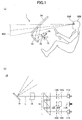
- Fig. 1 is a drawing illustrating an exemplary configuration of an optical system of an image display apparatus 1 according to the first embodiment.
- Fig. 1(a) is an exemplary overall configuration of the image display apparatus 1
- Fig. 1(b) is an exemplary configuration of an optical scanning apparatus 10 of the image display apparatus 1.
- the light-emitting elements 11R, 11G, and 11B are capable of emitting light beams having different wavelengths ⁇ R, ⁇ G, and ⁇ B.
- the wavelengths ⁇ R, ⁇ G, and ⁇ B may be, for example, 640 nm, 530 nm, and 445 nm, respectively.
- lasers, light emitting diode (LED) elements, second harmonic generation (SHG) elements, or the like may be used as the light-emitting elements 11R, 11G, and 11B.
- the light beams (diverging light) emitted from the light-emitting elements 11R, 11G, and 11B according to an image signal are converted to substantially parallel light or convergent light by corresponding coupling lenses 12R, 12G, and 12B, and are incident onto corresponding apertures 13R, 13G, and 13B.
- the coupling lenses 12R, 12G, and 12B convex glass lenses, plastic lenses, or the like may be used.
- the light beam which has been two-dimensionally deflected by the optical deflector 16 is incident onto the scan mirror 20, reflected by the scan mirror 20, and draws a two-dimensional image (intermediate image) on the scanned surface 30.
- the FPGA 600 is capable of causing the light-emitting elements 11R, 11G, and 11B to emit light and causing the optical deflector 16 to move for scanning by using the LD driver 612 and the optical deflector controller 614.
- the CPU 602 is capable of controlling functions of the image display apparatus 1.
- the ROM 604 is capable of storing an image processing program to be executed by the CPU 602 for controlling the functions of the image display apparatus 1.
- the RAM 606 is used as a work area of the CPU 602.
- the I/F 608 is an interface for communications with an external controller, etc., and is capable of connecting to, for example, a controller area network (CAN) of a car.
- CAN controller area network
- Fig. 3 is an exemplary functional block diagram of the image display apparatus 1 according to the first embodiment.
- the image display apparatus 1 includes as functional blocks a vehicle information input unit 700, an external information input unit 702, an image generation unit 704, an image display unit 706, etc.
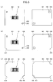
- Fig. 5(a) through Fig. 5(c) are exemplary plan views of a substrate 201 on which an optical deflector 16 is mounted. It should be noted that in each figure, a left side is a top view (planar view) and a right side is a bottom view.
- the housing 301 may be separated into a housing 301a and an optical deflector mounting member 301b with the protrusions 303.
- the housing 301a and the optical deflector mounting member 301b may be fixed to each other by any method such as adhesive fixation. It is desirable to use metal as a material of the optical deflector mounting member 301b, but a resin with a small linear expansion coefficient may also be used. In the case where a resin is used as the material of the optical deflector mounting member 301b, it is desirable to have, as the protrusions 303, metal pins extending from the optical deflector mounting member 301b.
- the positional adjustment is performed in directions of six axes (X, Y, Z, ⁇ , ⁇ , ⁇ ) shown in Fig. 7 in a state where the protrusions 303 of the housing 301 are inserted into the through holes 202 of the substrate 201 on which the optical deflector 16 is mounted.
- Fig. 8(a) through Fig. 8(c) are sectional views illustrating fixing the optical deflector 16. After the positional adjustment of the optical deflector 16 is completed in Fig. 6(b) , the optical deflector 16 is fixed to the housing 301.
- Fig. 8(a) shows a state in which the optical deflector 16 has a desired posture after the positional adjustment of the optical deflector 16 is completed in Fig. 6(b) .
- a protruding part 303a indicates a part of the protrusion 303 of the housing 301 protruding from the substrate 201 (herein after the protruding part 303a).
- a soldering iron may be used, or a method may be used in which, without using a soldering iron, hot air or laser light is used. It is preferable to use the method in which hot air or laser light is used, which does not put a load to the substrate 201 after the positional adjustment.
- the substrate 201 can be grounded.
- solder is physically and chemically stable as compared to adhesive, and reduced fixation strength or positional change is less likely to occur even under environmental conditions required for an automotive product, and thus, the positional relationship between the light beam L and the optical deflector 16 can be maintained stable for a long time.
- the state in which the position of the optical deflector 16 with respect to the light beam L is adjusted in six axis directions (X, Y, Z, ⁇ , ⁇ , ⁇ ) with high accuracy can be maintained stable for a long time.
- the environmental conditions required for an automotive product are, for example, an environmental condition in which the external environmental temperature is between about - 40 °C and + 85 °C.
- an optical scanning apparatus has been described in which an optical deflector with a single mirror is included.
- the optical deflector may be a DMD with multiple micro-mirrors.
- the present invention may be applied also to an optical scanning apparatus whose optical deflector is a DMD as in the case of an optical scanning apparatus whose optical deflector includes a single mirror.
Landscapes
- Physics & Mathematics (AREA)
- General Physics & Mathematics (AREA)
- Optics & Photonics (AREA)
- Electromagnetism (AREA)
- Mechanical Optical Scanning Systems (AREA)
- Transforming Electric Information Into Light Information (AREA)
- Instrument Panels (AREA)
Abstract
Description
- The present invention relates to an optical scanning apparatus, a substrate fixing method in the optical scanning apparatus, an image display apparatus, and a vehicle.
- In recent years, market expectations for a head-up display (HuD) mounted in a vehicle have been increasing as an application which enables a driver to recognize an alarm or information with little eye movement, and technology development of HuDs has been advanced. In particular, with the progress of in-vehicle sensing technologies represented by a term "advanced driving assistance system (ADAS)", driving environment information and passenger information have become available to be taken into the vehicle. Further, attention has been paid to a HuD as an "output of ADAS" for providing information to a driver.
- As a projection method of a HuD, a "panel method" is known in which an intermediate image is formed by an imaging device such as a liquid crystal display, a digital mirror device (DMD), or the like. Further, a "laser scan method" is known in which a laser beam emitted from a laser diode (hereinafter referred to as LD) is made to scan by a two-dimensional scanning device.
- In particular, in the latter laser scan method, different from the panel method in which an image is formed by partial light shielding of full screen emission, each pixel can be assigned to emission or non-emission, and thus, a high-contrast image can be formed.
- Meanwhile, high positional accuracy is required for a DMD in the panel method and an optical deflector of a HuD in the laser scan method, which deflector deflects a laser beam emitted from an LD. As a result, high-accuracy positional adjustment in six axes (X, Y, Z, α, β, γ) directions becomes necessary for an optical system which includes a light source, a condenser lens, etc. Further, in order to assure the reliability required for an automotive product such as a HuD, it is necessary that the deflector or the DMD is fixed by a high-reliability method.
- For example, in order to adjust a position of a MEMS module with high accuracy, a technique has been proposed in which positional adjustment is performed by aligning the MEMS module with a pin prepared beforehand on a base, and, after the positional adjustment, the MEMS module is fixed to the base by an adhesive or a screw (refer to, for example, Patent Document 1).
- In the above technique, the initial positional accuracy may be assured. However, under environmental conditions required for an automotive product, the position or the posture may change greatly and high reliability may not be assured.
- The present invention has been made by considering the above problem, and it is an object of the present invention to provide an optical scanning apparatus in which predetermined parts are fixed to each other in a state in which high reliability is assured even under the environmental conditions required for an automotive product.
- [Patent Document 1] Japanese Laid-Open Patent Application No.
2007-178523 - An optical scanning apparatus is provided. The optical scanning apparatus includes a light source, an optical deflector configured to deflect a light beam emitted from the light source to be scanned, a substrate configured to have the optical deflector mounted, and a housing configured to fix the substrate. The substrate includes a plurality of through holes, the housing includes protrusions corresponding to the through holes, and the substrate is fixed to the housing by using solder in a state where the protrusions are inserted into the through holes.
- Other objects, features and advantages of the present invention will become more apparent from the following detailed description when read in conjunction with the accompanying drawings.
-
-
Fig. 1 is a drawing illustrating an exemplary configuration of an optical system of an image display apparatus according to a first embodiment. -
Fig. 2 is a drawing illustrating an exemplary hardware configuration of the image display apparatus according to the first embodiment. -
Fig. 3 is an exemplary functional block diagram of the image display apparatus. -
Fig. 4 is an exemplary plan view of an optical deflector included in an optical scanning apparatus. -
Fig. 5 is an exemplary plan view of a substrate on which the optical deflector is mounted. -
Fig. 6 is a perspective view illustrating a housing to which the optical-deflector-mounted substrate is attached. -
Fig. 7 is a perspective view illustrating (six axis) directions in which a position of the optical deflector is adjusted. -
Fig. 8 is a sectional view illustrating fixing the optical deflector. - The following describes an embodiment of the present invention referring to the drawings. In the drawings, the same reference numerals are assigned to the same elements and duplicated descriptions may be omitted.
- In a first embodiment, an example will be described in which an image display apparatus including an optical scanning apparatus is applied to a HuD mounted in a vehicle (a car). The HuD is an apparatus which is mounted in a moving body including, for example, a vehicle, an airplane, and a ship, and which enables navigation information (information including speed, mileage, and the like) required for maneuvering the moving body to be recognized through a windshield, etc., of the moving body.
-
Fig. 1 is a drawing illustrating an exemplary configuration of an optical system of animage display apparatus 1 according to the first embodiment.Fig. 1(a) is an exemplary overall configuration of theimage display apparatus 1 andFig. 1(b) is an exemplary configuration of anoptical scanning apparatus 10 of theimage display apparatus 1. - As shown in
Fig. 1(a) , theimage display apparatus 1 includes theoptical scanning apparatus 10, ascan mirror 20, a scannedsurface 30 and areflection mirror 40. Theimage display apparatus 1 is an apparatus in which, by emitting light onto awindshield 50 of a vehicle, avirtual image 900 can be recognized byeyes 810 of adriver 800. - As shown in
Fig. 1(b) , theoptical scanning apparatus 10 includes light-emittingelements coupling lenses apertures composite element 14, alens 15, and anoptical deflector 16. It should be noted that the light-emittingelements - In the
optical scanning apparatus 10, the light-emittingelements elements - From the viewpoint of downsizing as well as assuring brightness and high image quality, it is preferable to use semiconductor lasers as the light-emitting
elements elements optical scanning apparatus 10. - The light beams (diverging light) emitted from the light-emitting
elements corresponding coupling lenses corresponding apertures coupling lenses - The
apertures apertures - The light beams shaped by the
apertures composite element 14. Because thecomposite element 14 has a function of synthesizing a single optical path by reflecting, or allowing penetration of, the light beams according to their wavelengths, the single optical path is synthesized from the three light beams having wavelengths λR, λG, and λB. Thecomposite element 14 may include, for example, a prismatic dichroic mirror. Thecomposite element 14 may also include a plurality of plate-like dichroic mirrors. - The
light deflector 16 deflects the light beam L to be scanned, which light beam has been synthesized by thecomposite element 14 from the light beams emitted from the light source, and forms a two-dimensional image on the scannedsurface 30. Specifically, the light beam L, whose optical path has been synthesized by thecomposite element 14, is guided to a reflection surface of theoptical deflector 16 by thelens 15. As thelens 15, for example, a single meniscus lens whose concave surface facing theoptical deflector 16 may be used. - The light beam L guided to the reflection surface of the
optical deflector 16 is two-dimensionally deflected by theoptical deflector 16. As theoptical deflector 16, for example, a minute mirror capable of swinging with respect to two axes orthogonal to each other, or two minute mirrors capable of swinging or rotating with respect to one axis may be used. Theoptical deflector 16 may be, for example, a MEMS produced by a semiconductor process, or the like. Theoptical deflector 16 may be driven by, for example, an actuator whose drive force is the deformation force of a piezoelectric element. - Referring to
Fig. 1(a) again, the light beam which has been two-dimensionally deflected by theoptical deflector 16 is incident onto thescan mirror 20, reflected by thescan mirror 20, and draws a two-dimensional image (intermediate image) on the scannedsurface 30. - The scanned
surface 30 is a surface having transparency onto which the light beam reflected by thescan mirror 20 is incident, and thus, a two-dimensional image is formed on the scannedsurface 30. The scannedsurface 30 has a function of diverging the incident light with a desired divergence angle. The scannedsurface 30 may have, for example, a micro lens array structure. As the scannedsurface 30, a diffuser panel may be used. - The light beam transmitted from the scanned
surface 30 is reflected by thereflex mirror 40, and incident onto thewindshield 50. In other words, the two-dimensional image formed on the scannedsurface 30 is projected on a reflection surface (a surface facing the driver 800) of thewindshield 50. As thereflex mirror 40, for example, a single concave mirror may be used. It is preferable that thereflex mirror 40 is designed and disposed in such a way that a component of optical strain is corrected, in which strain a horizontal line of the intermediate image becomes a convex or concave line due to an influence of thewindshield 50. - The
windshield 50 is a semi-transparent mirror which allows visible light to partially penetrate and partially be reflected. The light beam incident onto thewindshield 50 is partially reflected by thewindshield 50 and is incident onto theeyes 810 of thedriver 800. With the above mechanism, thedriver 800 can recognize an enlargedvirtual image 900 of the two-dimensional image on the scannedsurface 30 at a predetermined position of the front side (opposite side of the reflex surface of the windshield 50) of thewindshield 50. It should be noted that a separate semi-transparent mirror (combiner) which has the same function (partial reflection) as thewindshield 50 may be used. - Next, a hardware configuration and functional blocks of the
image display apparatus 1 will be described.Fig. 2 is a drawing illustrating an exemplary hardware configuration of theimage display apparatus 1 according to the first embodiment. Referring toFig. 2 , theimage display apparatus 1 includes anFPGA 600, aCPU 602, aROM 604, aRAM 606, an I/F 608, abus line 610, anLD driver 612, anoptical deflector controller 614, etc. - The
FPGA 600 is capable of causing the light-emittingelements optical deflector 16 to move for scanning by using theLD driver 612 and theoptical deflector controller 614. TheCPU 602 is capable of controlling functions of theimage display apparatus 1. TheROM 604 is capable of storing an image processing program to be executed by theCPU 602 for controlling the functions of theimage display apparatus 1. TheRAM 606 is used as a work area of theCPU 602. The I/F 608 is an interface for communications with an external controller, etc., and is capable of connecting to, for example, a controller area network (CAN) of a car. -
Fig. 3 is an exemplary functional block diagram of theimage display apparatus 1 according to the first embodiment. Referring toFig. 3 , theimage display apparatus 1 includes as functional blocks a vehicleinformation input unit 700, an externalinformation input unit 702, animage generation unit 704, animage display unit 706, etc. - Vehicle information (speed, mileage, etc.) from the CAN, etc., is input to the vehicle
information input unit 700. Information outside of vehicle from an external network (navigation information, etc., from GPS) is input to the externalinformation input unit 702. Theimage generation unit 704 generates an image to be displayed based on, for example, the information input from the vehicleinformation input unit 700 and the externalinformation input unit 702. - The
image display unit 706 includes, for example, acontrol unit 7061, and emits light onto thewindshield 50 by controlling theoptical scanning apparatus 10 by using thecontrol unit 7061. As a result, thedriver 800 can recognize an enlargedvirtual image 900 of the two-dimensional image on the scannedsurface 30 at a predetermined position on the front side of thewindshield 50. - The
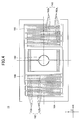
optical deflector 16 included in theoptical scanning apparatus 10 will be further described in detail.Fig. 4 is an exemplary plan view of theoptical deflector 16 included in theoptical scanning apparatus 10. It should be noted that inFig. 4 , it is assumed that an axis in which amirror 160 is supported is Y axis, an axis which is orthogonal to Y axis in a surface of aframe member 164 is X axis, and an axis which is orthogonal to X axis and Y axis (an axis normal to the surface of the frame member 164) is Z axis. - Referring to
Fig. 4 , theoptical deflector 16 is, for example, a MEMS produced by a semiconductor process, etc., and includes themirror 160 having a reflection surface. In both sides of themirror 160 in X axis direction, there is a pair of snake-like joist units 162 including a plurality of turn portions and having a snake-like shape. The snake-like joist units 162 includejoist units 162a andjoist units 162b which are disposed alternately, and are supported by aframe member 164. - In each of the
joist units piezoelectric members 166, warps are generated in thejoist units mirror 160 to rotate with a large angle around the X-axis (i.e., in a vertical direction). - With the above mechanism, it becomes possible to scan with light in the vertical direction around the X-axis by applying a low voltage. On the other hand, in the horizontal direction around the Y-axis, it is possible to scan with light by using resonance created by a torsion bar, or the like, which is connected to the
mirror 160. It should be noted that, here, anoptical deflector 16 is described as capable of scanning with light in two axis directions, X-axis and Y-axis. The structure illustrated inFig. 4 can be applied also to an optical deflector which is capable of scanning with light in a single axis direction. -
Fig. 5(a) through Fig. 5(c) are exemplary plan views of asubstrate 201 on which anoptical deflector 16 is mounted. It should be noted that in each figure, a left side is a top view (planar view) and a right side is a bottom view. - Referring to
Fig. 5(a) , theoptical deflector 16 is mounted on (fixed to) thesubstrate 201 and is electrically connected to theoptical defector controller 614, etc., (refer toFig. 2 ) mounted on thesubstrate 201. As thesubstrate 201, for example, a so-called epoxy glass substrate in which glass cloth is impregnated with an epoxy-based insulating resin, or a ceramic substrate may be used. - The
substrate 201 has a plurality of throughholes 202. In the case where a planar shape of thesubstrate 201 is rectangular, the throughholes 202 are disposed, for example, in two corners: any corner of thesubstrate 201 and its diagonal corner. In both sides of thesubstrate 201, metalized portions 203 (metal layer) formed of gold, copper, etc., are disposed around the through holes. It should be noted that the "planar shape" refers to a shape of an object when the object is viewed from a normal direction (Z direction inFig. 7 ) of a principal surface of the substrate 201 (hereinafter referred to the same). - In order to adjust a position of the
optical deflector 16, it is necessary to hold thesubstrate 201 by using a predetermined adjustment tool. Therefore, as shown inFig. 5(b) , it is preferable to havenotches 204 in one corner of thesubstrate 201 and its diagonal corner. With the above arrangement, it becomes easy to hold thesubstrate 201 when using the adjustment tool. - Further, as shown in
Fig. 5(c) , in place of the throughholes 202 shown inFig. 5(a) and Fig. 5(b) ,notches 205 may be formed in thesubstrate 201. With this arrangement, the size of the substrate 201 (planar shape) may be reduced. It should be noted that in both sides of thesubstrate 201, metalizedportions 203 formed of gold, copper, etc., are disposed near thenotches 205. -
Fig. 6(a) through Fig. 6(c) are perspective views illustrating ahousing 301 to which the optical-deflector-mountedsubstrate 201 is to be attached. - Inside of the
housing 301 shown inFig. 6(a) , optical elements shown inFig. 1(b) are housed. Further, after the position adjustment, thesubstrate 201 in which theoptical deflector 16 is mounted is fixed to asubstrate mounting surface 302 of thehousing 301 while theoptical deflector 16 faces the inside of thehousing 301. - The
substrate mounting surface 302 includesprotrusions 303 corresponding to the throughholes 202 of thesubstrate 201. In order to make smaller the positional change amounts of the optical elements due to temperature change, it is desirable to use metal as a material of thehousing 301. However, a resin may also be used whose linear expansion coefficient is small. In the case where a resin is used as a material of thehousing 301, it is desirable to have, as theprotrusions 303, metal pins extending from thehousing 301. - Relationship between a hole diameter (inner diameter) of the through
holes 202 of thesubstrate 201 and an outer diameter of theprotrusions 303 of thehousing 301 is determined by considering an amount of positional adjustment of theoptical deflector 16, rigidity of theprotrusions 303, heat capacity for melting solder 401 (to be described later), etc. - As shown in
Fig. 6(b) , positional relationship between theoptical deflector 16 and the light beam L is adjusted by moving the position of thesubstrate 201 with respect to thehousing 301 in a state where theprotrusions 303 of thehousing 301 are inserted into the throughholes 202 of thesubstrate 201 on which theoptical deflector 16 is mounted. During the position adjustment, thesubstrate 201 is held by a predetermined adjustment tool, and a desired posture of theoptical deflector 16 is obtained by moving the predetermined adjustment tool. - It should be noted that in order to make simple the shape of the
housing 301, as shown inFig. 6(c) , thehousing 301 may be separated into ahousing 301a and an opticaldeflector mounting member 301b with theprotrusions 303. Thehousing 301a and the opticaldeflector mounting member 301b may be fixed to each other by any method such as adhesive fixation. It is desirable to use metal as a material of the opticaldeflector mounting member 301b, but a resin with a small linear expansion coefficient may also be used. In the case where a resin is used as the material of the opticaldeflector mounting member 301b, it is desirable to have, as theprotrusions 303, metal pins extending from the opticaldeflector mounting member 301b. - It should be noted that in
Fig. 6(b) , the positional adjustment is performed in directions of six axes (X, Y, Z, α, β, γ) shown inFig. 7 in a state where theprotrusions 303 of thehousing 301 are inserted into the throughholes 202 of thesubstrate 201 on which theoptical deflector 16 is mounted. -
Fig. 8(a) through Fig. 8(c) are sectional views illustrating fixing theoptical deflector 16. After the positional adjustment of theoptical deflector 16 is completed inFig. 6(b) , theoptical deflector 16 is fixed to thehousing 301.Fig. 8(a) shows a state in which theoptical deflector 16 has a desired posture after the positional adjustment of theoptical deflector 16 is completed inFig. 6(b) . It should be noted that inFig. 8(a) , a protrudingpart 303a indicates a part of theprotrusion 303 of thehousing 301 protruding from the substrate 201 (herein after theprotruding part 303a). - After the state shown in
Fig. 8(a) , as shown inFig. 8(b) , meltedsolder 401 is supplied to theprotruding part 303a and the metalizedportion 203 of thesubstrate 201. By naturally cooling or forcibly cooling the meltedsolder 401, themetal protruding portion 303a and the metalizedportion 203 are joined by thesolder 401, and thesubstrate 201 and thehousing 301 are fixed to each other. With the above operation, the positional relationship between theoptical deflector 16 and the light beam L can be fixed in the desired state. - It should be noted that linear-shaped
solder 401a can be used as thesolder 401 as shown inFig. 8(c) . Or, by using preformedsolder 401b whose planar shape is like a donut as shown inFig. 8(c) , thesolder 401b may be put around the protrudingpart 303a in advance before the positional adjustment of theoptical deflector 16. - Further, as a method for melting the
solder 401, a soldering iron may be used, or a method may be used in which, without using a soldering iron, hot air or laser light is used. It is preferable to use the method in which hot air or laser light is used, which does not put a load to thesubstrate 201 after the positional adjustment. - Further, in the case where the material of the
housing 301 is metal and the metalizedportion 203 of thesubstrate 201 is a ground layer, the ground layer of thesubstrate 201 and theprotrusion 303 are electrically joined by thesolder 401, and thus, thesubstrate 201 can be grounded. - It should be noted that it is possible to fix the
protrusion 303 of thehousing 301 to thesubstrate 201 by using adhesive instead of thesolder 401. However, in the case where the adhesive is used, it becomes difficult to readjust the position of theoptical deflector 16 or reuse theoptical deflector 16. On the other hand, in the case where thesolder 401 is used for fixing theprotrusion 303 of thehousing 301 to thesubstrate 201, by melting thesolder 401 again, it becomes possible to easily readjust the position of theoptical deflector 16 or reuse theoptical deflector 16. - Further, solder is physically and chemically stable as compared to adhesive, and reduced fixation strength or positional change is less likely to occur even under environmental conditions required for an automotive product, and thus, the positional relationship between the light beam L and the
optical deflector 16 can be maintained stable for a long time. In other words, the state in which the position of theoptical deflector 16 with respect to the light beam L is adjusted in six axis directions (X, Y, Z, α, β, γ) with high accuracy can be maintained stable for a long time. It should be noted that the environmental conditions required for an automotive product are, for example, an environmental condition in which the external environmental temperature is between about - 40 °C and + 85 °C. - The preferred embodiments have been described above. However, the embodiments are not limited to those described above, and various modifications and replacements may be applied to the above embodiments without departing from the scope of the present invention.
- For example, in the above embodiment, an optical scanning apparatus has been described in which an optical deflector with a single mirror is included. However, the optical deflector may be a DMD with multiple micro-mirrors. The present invention may be applied also to an optical scanning apparatus whose optical deflector is a DMD as in the case of an optical scanning apparatus whose optical deflector includes a single mirror.
- The present application is based on and claims the benefit of priority of Japanese Priority Application No.
2015-045073 filed on March 6, 2015
Claims (10)
- An optical scanning apparatus comprising:a light source;an optical deflector configured to deflect a light beam emitted from the light source to scan;a substrate configured to have the optical deflector mounted; anda housing configured to fix the substrate, whereinthe substrate includes a plurality of through holes,the housing includes protrusions corresponding to the through holes, andthe substrate is fixed to the housing by using solder in a state where the protrusions are inserted into the through holes.
- The optical scanning apparatus according to claim 1, wherein
the protrusions are metal,
a metal layer is disposed around each of the through holes, and
the metal and the metal layer are joined by the solder. - The optical scanning apparatus according to claim 1 or 2, wherein
the substrate is rectangular,
the through holes are disposed at a first corner of the substrate and a second corner positioned diagonal to the first corner. - An image display apparatus comprising the optical scanning apparatus according to any one of claims 1 through 3.
- The image display apparatus according to claim 4, wherein
the light source includes a plurality of light-emitting elements,
after light beams emitted from the light-emitting elements are synthesized into a single light beam, the single light beam is deflected to scan to form a two-dimensional image on a scanned surface, and
the two-dimensional image is projected onto a reflex surface of a semi-transparent mirror which allows visible light to partially penetrate and partially be reflected. - The image display apparatus according to claim 5, wherein
an enlarged virtual image of the two-dimensional image is formed at a predetermined position of an opposite side of the reflex surface of the semi-transparent mirror. - A vehicle comprising:the image display apparatus according to claim 5 or 6, whereina driver recognizes an enlarged virtual image of the two-dimensional image at a predetermined position in front of the reflex surface of the semi-transparent mirror.
- A substrate fixing method in an optical scanning apparatus having a light source fixed in a housing and a substrate on which an optical deflector is mounted, the optical deflector deflecting a light beam emitted from the light source to scan, the method comprising:inserting a plurality of protrusions disposed in the housing into a plurality of through holes disposed in the substrate;adjusting a positional relationship between the optical deflector and the light beam by moving a position of the substrate with respect to the housing in a state where the protrusions are inserted into the through holes; andfixing the substrate to the housing by using solder after the adjusting is completed.
- The substrate fixing method according to claim 8, wherein
the protrusions are metal,
a metal layer is disposed around each of the through holes, and in the fixing, the metal and the metal layer are joined by the solder. - The substrate fixing method according to claim 8 or 9, wherein
the substrate is rectangular,
the through holes are disposed at a first corner of the substrate and a second corner positioned diagonal to the first corner.
Applications Claiming Priority (1)
| Application Number | Priority Date | Filing Date | Title |
|---|---|---|---|
| JP2015045073A JP6524722B2 (en) | 2015-03-06 | 2015-03-06 | Optical scanning device, fixing method of substrate in optical scanning device, image display device, vehicle |
Publications (2)
| Publication Number | Publication Date |
|---|---|
| EP3064975A1 true EP3064975A1 (en) | 2016-09-07 |
| EP3064975B1 EP3064975B1 (en) | 2019-01-23 |
Family
ID=55411298
Family Applications (1)
| Application Number | Title | Priority Date | Filing Date |
|---|---|---|---|
| EP16157043.7A Not-in-force EP3064975B1 (en) | 2015-03-06 | 2016-02-24 | Optical scanning apparatus, substrate fixing method in optical scanning apparatus, image display apparatus, and vehicle |
Country Status (2)
| Country | Link |
|---|---|
| EP (1) | EP3064975B1 (en) |
| JP (1) | JP6524722B2 (en) |
Cited By (2)
| Publication number | Priority date | Publication date | Assignee | Title |
|---|---|---|---|---|
| EP3660577A1 (en) * | 2018-11-28 | 2020-06-03 | Ricoh Company, Ltd. | Display device and mobile body |
| DE102019131279A1 (en) * | 2019-11-20 | 2021-05-20 | Valeo Schalter Und Sensoren Gmbh | Head-up display with adhesive as a tolerance compensation compound between an optical component and a receiving element, as well as an assembly process |
Families Citing this family (1)
| Publication number | Priority date | Publication date | Assignee | Title |
|---|---|---|---|---|
| JP2021089412A (en) * | 2019-11-21 | 2021-06-10 | 株式会社リコー | Light reflection device and movable body |
Citations (6)
| Publication number | Priority date | Publication date | Assignee | Title |
|---|---|---|---|---|
| EP1087248A1 (en) * | 1999-02-26 | 2001-03-28 | The Nippon Signal Co. Ltd. | Planar optical scanner and its mounting structure |
| JP2007178523A (en) | 2005-12-27 | 2007-07-12 | Nikon Corp | Wavelength selective switch |
| JP2009154264A (en) * | 2007-12-27 | 2009-07-16 | Stanley Electric Co Ltd | MEMS module |
| EP2570843A1 (en) * | 2011-09-14 | 2013-03-20 | Ricoh Company Ltd. | Head-up display for a vehicle |
| US20130327834A1 (en) * | 2012-06-10 | 2013-12-12 | Metrologic Instruments, Inc. | Laser scanning module with rotatably adjustable laser scanning assembly |
| WO2014103803A1 (en) * | 2012-12-28 | 2014-07-03 | 株式会社Jvcケンウッド | Mems optical scanner |
Family Cites Families (2)
| Publication number | Priority date | Publication date | Assignee | Title |
|---|---|---|---|---|
| JP2007150708A (en) * | 2005-11-28 | 2007-06-14 | Kyocera Corp | Imaging module and imaging apparatus |
| JP2008076628A (en) * | 2006-09-20 | 2008-04-03 | Kyocera Corp | Imaging module and imaging apparatus |
-
2015
- 2015-03-06 JP JP2015045073A patent/JP6524722B2/en not_active Expired - Fee Related
-
2016
- 2016-02-24 EP EP16157043.7A patent/EP3064975B1/en not_active Not-in-force
Patent Citations (6)
| Publication number | Priority date | Publication date | Assignee | Title |
|---|---|---|---|---|
| EP1087248A1 (en) * | 1999-02-26 | 2001-03-28 | The Nippon Signal Co. Ltd. | Planar optical scanner and its mounting structure |
| JP2007178523A (en) | 2005-12-27 | 2007-07-12 | Nikon Corp | Wavelength selective switch |
| JP2009154264A (en) * | 2007-12-27 | 2009-07-16 | Stanley Electric Co Ltd | MEMS module |
| EP2570843A1 (en) * | 2011-09-14 | 2013-03-20 | Ricoh Company Ltd. | Head-up display for a vehicle |
| US20130327834A1 (en) * | 2012-06-10 | 2013-12-12 | Metrologic Instruments, Inc. | Laser scanning module with rotatably adjustable laser scanning assembly |
| WO2014103803A1 (en) * | 2012-12-28 | 2014-07-03 | 株式会社Jvcケンウッド | Mems optical scanner |
Cited By (2)
| Publication number | Priority date | Publication date | Assignee | Title |
|---|---|---|---|---|
| EP3660577A1 (en) * | 2018-11-28 | 2020-06-03 | Ricoh Company, Ltd. | Display device and mobile body |
| DE102019131279A1 (en) * | 2019-11-20 | 2021-05-20 | Valeo Schalter Und Sensoren Gmbh | Head-up display with adhesive as a tolerance compensation compound between an optical component and a receiving element, as well as an assembly process |
Also Published As
| Publication number | Publication date |
|---|---|
| EP3064975B1 (en) | 2019-01-23 |
| JP6524722B2 (en) | 2019-06-05 |
| JP2016164632A (en) | 2016-09-08 |
Similar Documents
| Publication | Publication Date | Title |
|---|---|---|
| US10983423B2 (en) | Image display device | |
| US10831021B2 (en) | Display device and including a screen concave mirror and flat mirror | |
| US10156351B2 (en) | Temperature control device, image display apparatus and vehicle | |
| US11131850B2 (en) | Display apparatus and equipment | |
| US10613321B2 (en) | Image display apparatus | |
| EP3805839B1 (en) | Light deflector, deflecting device, distance-measuring apparatus, image projection device, and vehicle | |
| JP6492966B2 (en) | Light source unit and image display device | |
| JP6627886B2 (en) | Optical scanning device, image display device, and vehicle | |
| US11624903B2 (en) | Light deflector, LiDAR device, and image forming apparatus | |
| JP2020101588A (en) | Movable device, distance measuring device, image projection device, vehicle, and pedestal | |
| JP2020101587A (en) | Movable device, distance measuring device, image projection device, and vehicle | |
| US20220299757A1 (en) | Movable device, image projection apparatus, laser headlamp, head-mounted display, distance measurement device, and mobile object | |
| EP3064975B1 (en) | Optical scanning apparatus, substrate fixing method in optical scanning apparatus, image display apparatus, and vehicle | |
| EP4270084B1 (en) | Optical scanning device | |
| JP7151423B2 (en) | display and mobile | |
| US11262582B2 (en) | Display device and mobile object | |
| US11971537B2 (en) | Light deflection device, distance measurement device, and mobile body | |
| US7573626B2 (en) | Optical scanner and image display apparatus having the same | |
| JP2017223893A (en) | Optical device, optical unit, display device, and prism fixation method | |
| JP2017142882A (en) | Light source device and image display device | |
| US12379587B2 (en) | Light deflector, image projection apparatus, laser headlamp, head-mounted display, distance measurement apparatus, and mobile object | |
| JP7363604B2 (en) | Optical scanning devices, head-up displays, and mobile objects | |
| JP2021144131A (en) | Display device and mobile body | |
| JP6515638B2 (en) | Optical scanner, image display device and head mounted display | |
| JP2020086218A (en) | Display unit and movable body |
Legal Events
| Date | Code | Title | Description |
|---|---|---|---|
| PUAI | Public reference made under article 153(3) epc to a published international application that has entered the european phase |
Free format text: ORIGINAL CODE: 0009012 |
|
| 17P | Request for examination filed |
Effective date: 20160224 |
|
| AK | Designated contracting states |
Kind code of ref document: A1 Designated state(s): AL AT BE BG CH CY CZ DE DK EE ES FI FR GB GR HR HU IE IS IT LI LT LU LV MC MK MT NL NO PL PT RO RS SE SI SK SM TR |
|
| AX | Request for extension of the european patent |
Extension state: BA ME |
|
| STAA | Information on the status of an ep patent application or granted ep patent |
Free format text: STATUS: EXAMINATION IS IN PROGRESS |
|
| 17Q | First examination report despatched |
Effective date: 20171205 |
|
| GRAP | Despatch of communication of intention to grant a patent |
Free format text: ORIGINAL CODE: EPIDOSNIGR1 |
|
| STAA | Information on the status of an ep patent application or granted ep patent |
Free format text: STATUS: GRANT OF PATENT IS INTENDED |
|
| RIC1 | Information provided on ipc code assigned before grant |
Ipc: G02B 26/10 20060101ALI20180705BHEP Ipc: G02B 26/08 20060101ALI20180705BHEP Ipc: G02B 27/01 20060101ALN20180705BHEP Ipc: G02B 7/182 20060101AFI20180705BHEP |
|
| INTG | Intention to grant announced |
Effective date: 20180807 |
|
| GRAS | Grant fee paid |
Free format text: ORIGINAL CODE: EPIDOSNIGR3 |
|
| GRAA | (expected) grant |
Free format text: ORIGINAL CODE: 0009210 |
|
| STAA | Information on the status of an ep patent application or granted ep patent |
Free format text: STATUS: THE PATENT HAS BEEN GRANTED |
|
| AK | Designated contracting states |
Kind code of ref document: B1 Designated state(s): AL AT BE BG CH CY CZ DE DK EE ES FI FR GB GR HR HU IE IS IT LI LT LU LV MC MK MT NL NO PL PT RO RS SE SI SK SM TR |
|
| REG | Reference to a national code |
Ref country code: GB Ref legal event code: FG4D |
|
| REG | Reference to a national code |
Ref country code: CH Ref legal event code: EP |
|
| REG | Reference to a national code |
Ref country code: AT Ref legal event code: REF Ref document number: 1091908 Country of ref document: AT Kind code of ref document: T Effective date: 20190215 |
|
| REG | Reference to a national code |
Ref country code: IE Ref legal event code: FG4D |
|
| REG | Reference to a national code |
Ref country code: DE Ref legal event code: R096 Ref document number: 602016009318 Country of ref document: DE |
|
| REG | Reference to a national code |
Ref country code: NL Ref legal event code: MP Effective date: 20190123 |
|
| PG25 | Lapsed in a contracting state [announced via postgrant information from national office to epo] |
Ref country code: NL Free format text: LAPSE BECAUSE OF FAILURE TO SUBMIT A TRANSLATION OF THE DESCRIPTION OR TO PAY THE FEE WITHIN THE PRESCRIBED TIME-LIMIT Effective date: 20190123 |
|
| PG25 | Lapsed in a contracting state [announced via postgrant information from national office to epo] |
Ref country code: ES Free format text: LAPSE BECAUSE OF FAILURE TO SUBMIT A TRANSLATION OF THE DESCRIPTION OR TO PAY THE FEE WITHIN THE PRESCRIBED TIME-LIMIT Effective date: 20190123 Ref country code: LT Free format text: LAPSE BECAUSE OF FAILURE TO SUBMIT A TRANSLATION OF THE DESCRIPTION OR TO PAY THE FEE WITHIN THE PRESCRIBED TIME-LIMIT Effective date: 20190123 Ref country code: PL Free format text: LAPSE BECAUSE OF FAILURE TO SUBMIT A TRANSLATION OF THE DESCRIPTION OR TO PAY THE FEE WITHIN THE PRESCRIBED TIME-LIMIT Effective date: 20190123 Ref country code: FI Free format text: LAPSE BECAUSE OF FAILURE TO SUBMIT A TRANSLATION OF THE DESCRIPTION OR TO PAY THE FEE WITHIN THE PRESCRIBED TIME-LIMIT Effective date: 20190123 Ref country code: SE Free format text: LAPSE BECAUSE OF FAILURE TO SUBMIT A TRANSLATION OF THE DESCRIPTION OR TO PAY THE FEE WITHIN THE PRESCRIBED TIME-LIMIT Effective date: 20190123 Ref country code: NO Free format text: LAPSE BECAUSE OF FAILURE TO SUBMIT A TRANSLATION OF THE DESCRIPTION OR TO PAY THE FEE WITHIN THE PRESCRIBED TIME-LIMIT Effective date: 20190423 Ref country code: PT Free format text: LAPSE BECAUSE OF FAILURE TO SUBMIT A TRANSLATION OF THE DESCRIPTION OR TO PAY THE FEE WITHIN THE PRESCRIBED TIME-LIMIT Effective date: 20190523 |
|
| REG | Reference to a national code |
Ref country code: AT Ref legal event code: MK05 Ref document number: 1091908 Country of ref document: AT Kind code of ref document: T Effective date: 20190123 |
|
| PG25 | Lapsed in a contracting state [announced via postgrant information from national office to epo] |
Ref country code: GR Free format text: LAPSE BECAUSE OF FAILURE TO SUBMIT A TRANSLATION OF THE DESCRIPTION OR TO PAY THE FEE WITHIN THE PRESCRIBED TIME-LIMIT Effective date: 20190424 Ref country code: HR Free format text: LAPSE BECAUSE OF FAILURE TO SUBMIT A TRANSLATION OF THE DESCRIPTION OR TO PAY THE FEE WITHIN THE PRESCRIBED TIME-LIMIT Effective date: 20190123 Ref country code: RS Free format text: LAPSE BECAUSE OF FAILURE TO SUBMIT A TRANSLATION OF THE DESCRIPTION OR TO PAY THE FEE WITHIN THE PRESCRIBED TIME-LIMIT Effective date: 20190123 Ref country code: BG Free format text: LAPSE BECAUSE OF FAILURE TO SUBMIT A TRANSLATION OF THE DESCRIPTION OR TO PAY THE FEE WITHIN THE PRESCRIBED TIME-LIMIT Effective date: 20190423 Ref country code: LV Free format text: LAPSE BECAUSE OF FAILURE TO SUBMIT A TRANSLATION OF THE DESCRIPTION OR TO PAY THE FEE WITHIN THE PRESCRIBED TIME-LIMIT Effective date: 20190123 Ref country code: IS Free format text: LAPSE BECAUSE OF FAILURE TO SUBMIT A TRANSLATION OF THE DESCRIPTION OR TO PAY THE FEE WITHIN THE PRESCRIBED TIME-LIMIT Effective date: 20190523 |
|
| REG | Reference to a national code |
Ref country code: CH Ref legal event code: PL |
|
| REG | Reference to a national code |
Ref country code: DE Ref legal event code: R097 Ref document number: 602016009318 Country of ref document: DE |
|
| PG25 | Lapsed in a contracting state [announced via postgrant information from national office to epo] |
Ref country code: RO Free format text: LAPSE BECAUSE OF FAILURE TO SUBMIT A TRANSLATION OF THE DESCRIPTION OR TO PAY THE FEE WITHIN THE PRESCRIBED TIME-LIMIT Effective date: 20190123 Ref country code: SK Free format text: LAPSE BECAUSE OF FAILURE TO SUBMIT A TRANSLATION OF THE DESCRIPTION OR TO PAY THE FEE WITHIN THE PRESCRIBED TIME-LIMIT Effective date: 20190123 Ref country code: CZ Free format text: LAPSE BECAUSE OF FAILURE TO SUBMIT A TRANSLATION OF THE DESCRIPTION OR TO PAY THE FEE WITHIN THE PRESCRIBED TIME-LIMIT Effective date: 20190123 Ref country code: MC Free format text: LAPSE BECAUSE OF FAILURE TO SUBMIT A TRANSLATION OF THE DESCRIPTION OR TO PAY THE FEE WITHIN THE PRESCRIBED TIME-LIMIT Effective date: 20190123 Ref country code: AL Free format text: LAPSE BECAUSE OF FAILURE TO SUBMIT A TRANSLATION OF THE DESCRIPTION OR TO PAY THE FEE WITHIN THE PRESCRIBED TIME-LIMIT Effective date: 20190123 Ref country code: LU Free format text: LAPSE BECAUSE OF NON-PAYMENT OF DUE FEES Effective date: 20190224 Ref country code: EE Free format text: LAPSE BECAUSE OF FAILURE TO SUBMIT A TRANSLATION OF THE DESCRIPTION OR TO PAY THE FEE WITHIN THE PRESCRIBED TIME-LIMIT Effective date: 20190123 Ref country code: IT Free format text: LAPSE BECAUSE OF FAILURE TO SUBMIT A TRANSLATION OF THE DESCRIPTION OR TO PAY THE FEE WITHIN THE PRESCRIBED TIME-LIMIT Effective date: 20190123 Ref country code: DK Free format text: LAPSE BECAUSE OF FAILURE TO SUBMIT A TRANSLATION OF THE DESCRIPTION OR TO PAY THE FEE WITHIN THE PRESCRIBED TIME-LIMIT Effective date: 20190123 |
|
| REG | Reference to a national code |
Ref country code: BE Ref legal event code: MM Effective date: 20190228 |
|
| REG | Reference to a national code |
Ref country code: IE Ref legal event code: MM4A |
|
| PG25 | Lapsed in a contracting state [announced via postgrant information from national office to epo] |
Ref country code: SM Free format text: LAPSE BECAUSE OF FAILURE TO SUBMIT A TRANSLATION OF THE DESCRIPTION OR TO PAY THE FEE WITHIN THE PRESCRIBED TIME-LIMIT Effective date: 20190123 |
|
| PLBE | No opposition filed within time limit |
Free format text: ORIGINAL CODE: 0009261 |
|
| STAA | Information on the status of an ep patent application or granted ep patent |
Free format text: STATUS: NO OPPOSITION FILED WITHIN TIME LIMIT |
|
| PG25 | Lapsed in a contracting state [announced via postgrant information from national office to epo] |
Ref country code: CH Free format text: LAPSE BECAUSE OF NON-PAYMENT OF DUE FEES Effective date: 20190228 Ref country code: LI Free format text: LAPSE BECAUSE OF NON-PAYMENT OF DUE FEES Effective date: 20190228 Ref country code: AT Free format text: LAPSE BECAUSE OF FAILURE TO SUBMIT A TRANSLATION OF THE DESCRIPTION OR TO PAY THE FEE WITHIN THE PRESCRIBED TIME-LIMIT Effective date: 20190123 |
|
| 26N | No opposition filed |
Effective date: 20191024 |
|
| PG25 | Lapsed in a contracting state [announced via postgrant information from national office to epo] |
Ref country code: IE Free format text: LAPSE BECAUSE OF NON-PAYMENT OF DUE FEES Effective date: 20190224 |
|
| PG25 | Lapsed in a contracting state [announced via postgrant information from national office to epo] |
Ref country code: SI Free format text: LAPSE BECAUSE OF FAILURE TO SUBMIT A TRANSLATION OF THE DESCRIPTION OR TO PAY THE FEE WITHIN THE PRESCRIBED TIME-LIMIT Effective date: 20190123 Ref country code: BE Free format text: LAPSE BECAUSE OF NON-PAYMENT OF DUE FEES Effective date: 20190228 |
|
| PG25 | Lapsed in a contracting state [announced via postgrant information from national office to epo] |
Ref country code: TR Free format text: LAPSE BECAUSE OF FAILURE TO SUBMIT A TRANSLATION OF THE DESCRIPTION OR TO PAY THE FEE WITHIN THE PRESCRIBED TIME-LIMIT Effective date: 20190123 |
|
| PG25 | Lapsed in a contracting state [announced via postgrant information from national office to epo] |
Ref country code: MT Free format text: LAPSE BECAUSE OF NON-PAYMENT OF DUE FEES Effective date: 20190224 |
|
| PGFP | Annual fee paid to national office [announced via postgrant information from national office to epo] |
Ref country code: FR Payment date: 20210226 Year of fee payment: 6 |
|
| PG25 | Lapsed in a contracting state [announced via postgrant information from national office to epo] |
Ref country code: CY Free format text: LAPSE BECAUSE OF FAILURE TO SUBMIT A TRANSLATION OF THE DESCRIPTION OR TO PAY THE FEE WITHIN THE PRESCRIBED TIME-LIMIT Effective date: 20190123 |
|
| PGFP | Annual fee paid to national office [announced via postgrant information from national office to epo] |
Ref country code: DE Payment date: 20210217 Year of fee payment: 6 Ref country code: GB Payment date: 20210224 Year of fee payment: 6 |
|
| PG25 | Lapsed in a contracting state [announced via postgrant information from national office to epo] |
Ref country code: HU Free format text: LAPSE BECAUSE OF FAILURE TO SUBMIT A TRANSLATION OF THE DESCRIPTION OR TO PAY THE FEE WITHIN THE PRESCRIBED TIME-LIMIT; INVALID AB INITIO Effective date: 20160224 |
|
| PG25 | Lapsed in a contracting state [announced via postgrant information from national office to epo] |
Ref country code: MK Free format text: LAPSE BECAUSE OF FAILURE TO SUBMIT A TRANSLATION OF THE DESCRIPTION OR TO PAY THE FEE WITHIN THE PRESCRIBED TIME-LIMIT Effective date: 20190123 |
|
| REG | Reference to a national code |
Ref country code: DE Ref legal event code: R119 Ref document number: 602016009318 Country of ref document: DE |
|
| GBPC | Gb: european patent ceased through non-payment of renewal fee |
Effective date: 20220224 |
|
| PG25 | Lapsed in a contracting state [announced via postgrant information from national office to epo] |
Ref country code: FR Free format text: LAPSE BECAUSE OF NON-PAYMENT OF DUE FEES Effective date: 20220228 |
|
| PG25 | Lapsed in a contracting state [announced via postgrant information from national office to epo] |
Ref country code: GB Free format text: LAPSE BECAUSE OF NON-PAYMENT OF DUE FEES Effective date: 20220224 Ref country code: DE Free format text: LAPSE BECAUSE OF NON-PAYMENT OF DUE FEES Effective date: 20220901 |